AppNote 411
Copyright 2002, EM Microelectronic-Marin SA 1 www.emmicroelectronic.com
Application Note 411Title: RFID Made EasyProduct Family: RFID
Part Number: EM RFID ProductsKeywords: RFID techniques, RFID Principles, Antenna Design, Theory, System DesignDate: 25 September 2002
TABLE OF CONTENT
1 Introduction.......................................................................................................................................................................21.1 EM Microelectronic transponder systems..................................................................................................................21.2 Future trends in transponder systems .......................................................................................................................31.3 Frequency spectrum..................................................................................................................................................3
2 System principles .............................................................................................................................................................52.1 System setup.............................................................................................................................................................52.2 Electromagnetic field theory ......................................................................................................................................62.3 Magnetic field and inductivity.....................................................................................................................................72.4 Transformer principles and magnetic coupling ..........................................................................................................72.5 Quality factor, phase shift and bandwidth..................................................................................................................8
3 Antenna design...............................................................................................................................................................103.1 General resonant circuit parameters .......................................................................................................................103.2 Antenna parameters ................................................................................................................................................113.3 Antenna fine tuning..................................................................................................................................................12
4 Data Coding/Encoding....................................................................................................................................................134.1 Non-return to Zero Modulation (NRZ)......................................................................................................................134.2 Return to Zero Modulation (RZ)...............................................................................................................................134.3 Manchester Coding .................................................................................................................................................14
4.3.1 Differential Manchester Coding ...................................................................................................................144.4 Biphase Coding .......................................................................................................................................................15
4.4.1 Differential Biphase Coding .........................................................................................................................154.5 Miller Coding ...........................................................................................................................................................154.6 Phase Shift Keying ..................................................................................................................................................16
5 Bibliography....................................................................................................................................................................176 Glossary .........................................................................................................................................................................177 Appendix.........................................................................................................................................................................18
7.1 Institutes ..................................................................................................................................................................187.2 Trade fairs: ..............................................................................................................................................................187.3 Copper Wire List......................................................................................................................................................18
EM MICROELECTRONIC - MARIN SA
AppNote 411
Copyright 2002, EM Microelectronic-Marin SA 2 www.emmicroelectronic.com
1 IntroductionThe recent years showed an immense increase inquantity of Radio Frequency Identification (RFID)semiconductors such as transponders and transceivercircuits. Many system house companies with main forcesin software or hardware design become more interestedin that new technology. The high integration of RFIDcircuits allows a relatively easy implementation into anycustomer specific application. Nevertheless, you willneed some basic knowledge of RF theory to achieve themaximum performance in your system.The aim of this RFID Design Guide is to give you therelevant guidelines for your design using standardintegrated circuits.
1.1 EM Microelectronic transponder systemsThe Contactless Identification activity began in 1989 andtoday comprises some 50 products in production, whichare used in a huge quantity of application like AccessControl, Animal Identification, Car Immobilisation,Laundry Tagging, Logistic, Sports Performance etc[Bibliography B4].
Figure 1: Transponders packed as disks
Figure 2: Transponders in keys
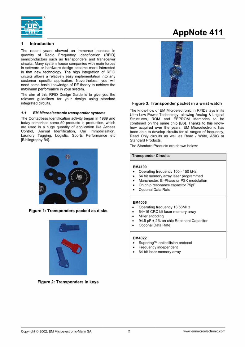
Figure 3: Transponder packet in a wrist watchThe know-how of EM Microelectronic in RFIDs lays in itsUltra Low Power Technology, allowing Analog & LogicalStructures, ROM and EEPROM Memories to becombined on the same chip [B6]. Thanks to this know-how acquired over the years, EM Microelectronic hasbeen able to develop circuits for all ranges of frequency,Read Only circuits as well as Read / Write, ASIC orStandard Products.The Standard Products are shown below:
Transponder Circuits
EM4100• Operating frequency 100 - 150 kHz• 64 bit memory array laser programmed• Manchester, Bi-Phase or PSK modulation• On chip resonance capacitor 75pF• Optional Data Rate
EM4006• Operating frequency 13.56MHz• 64+16 CRC bit laser memory array• Miller encoding• 94.5 pF ± 2% on chip Resonant Capacitor• Optional Data Rate
EM4022• Supertag™ anticollision protocol• Frequency independent• 64 bit laser memory array

AppNote 411
Copyright 2002, EM Microelectronic-Marin SA 3 www.emmicroelectronic.com
EM4069• Operating frequency 100 - 150 kHz• 128 bit EEPROM• OTP feature convert EEPROM words in Read Only• 64 bit fixed code memory array laser programmed• Data encoding : Manchester or Bi-phase• Transmission reader to chip : 65% AM modulation• Data rate : 2 or 4 Kbaud• 75pF on chip Resonance Capacitor
EM4005• Operating frequency 100 - 150 kHz• 128 bit memory array laser programmed• Bit coding according to ISO FDX-B• On chip resonance capacitor 75pF
EM4150• Operating frequency 100 - 150 kHz• 1 KBit of EEPROM• 32 bit Device Serial Number (Laser ROM)• 32 bit Device Identification (Laser ROM)• User defined Password• User defined Read Memory Area at Power On• User defined Write Inhibited Memory Area• User defined Read Protected Memory Area• 170 pF ± 2% on chip Resonant Capacitor• On chip Rectifier and Voltage Limiter
Transceiver Circuit
EM4095• PLL which adapts carrier frequency to antenna
resonant frequency• No external quartz required• 100kHz to 150kHz carrier frequency range• Data transmission performed by Amplitude
Modulation• Multiple transponder protocol compatibility
(EM400X, EM4050, EM4069 etc.)• Sleep mode 1µA• Antenna short circuit detection
Table 1: EM Microelectronic Standard Products
1.2 Future trends in transponder systemsWhat will bring us the future in RFID? There are threemain topics, where a constant improvement is takingplace:Design and Technology• Manufacturing methods• Frequency spectrum allocationThe low power design is a master key to low price RFIDchip production. With smaller structures the surface ofthe chip and the power can be reduced. Smaller chipsurfaces will bring new assembly technologies, such asflip-chip technology. Working with higher frequenciessuch as 13.56MHz or higher will reduce the number ofturns of the antenna, as well as the resonance capacity.Furthermore the data transmission rate can beincreased. With higher frequencies, longer readingranges occur. Thus, Multitag applications will becomemore important. Tradefares like Scantech are alwayspresenting trendsetting products [Appendix A5].EM Microelectronic will be able to profit from its 10 yearsexperience in RFID chip-design and manufacturing.
1.3 Frequency spectrumRFID systems are regarded as radio emitting devicesand therefore the international an domestic radioregulations are relevant. This means that the frequencyselection is restricted to a number of fixed frequencybands. The most common frequencies used are 0...135kHz, 400kHz, 6.78MHz, 13.56MHz, 27.125MHz,40.68MHz, 433.29MHz, 869MHz, 915MHz, 2.45GHz,5.8GHz and 24.125GHz [B3]. Frequencies are divided inthe following ranges:
Freq. Range [Hz] Wavelengthλλλλ [m]
Name Abbr.
3 ... 300 108 ... 106 extremely low freq. ELF300 ... 3k 106 ... 105 ultra low frequency ULF3k ... 30k 105 ... 104 very low frequency VLF30k ... 300k 104 ... 103 low frequency LF300k ... 3M 103 ... 102 medium frequency MF3M ... 30M 102 ... 101 high frequency HF30M ... 300M 101 ... 100 very high frequency VHF300M ... 3G 100 ... 10-1 ultra high frequency UHF3G ... 30G 10-1 ... 10-2 super high frequency SHF30G ... 3000G 10-2 ... 10-4 extremely high freq. EHF
Table 2: Normalised Frequency Ranges [B1]
AppNote 411
Copyright 2002, EM Microelectronic-Marin SA 4 www.emmicroelectronic.com
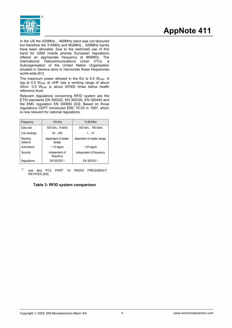
In the US the 420MHz... 460MHz band was not favouredbut therefore the 315MHz and 902MHz... 928MHz bandshave been allocated. Due to the restricted use of thisband for GSM mobile phones European regulationsoffered an appropriate frequency at 869MHz. TheInternational Telecommunications Union (ITU), aSuborganisation of the United Nation Organisationsituated in Geneva aims to harmonise these frequenciesworld-wide [A1].The maximum power allowed in the EU is 0.5 WERP. Atag at 0.5 WERP at UHF has a working range of about30cm. 0.5 WERP is about 50'000 times below healthreference level.Relevant regulations concerning RFID system are theETSI standards EN 300220, EN 300330, EN 300440 andthe EMC regulation EN 300683 [A3]. Based on thoseregulations CEPT introduced ERC 70-03 in 1997, whichis now relevant for national regulations.
Frequency 125 kHz 13.56 MHz
Data rate 500 bit/s... 8 kbit/s 500 bit/s... 106 kbit/s
Coil windings 40... 300 1... 10
Readingdistance
dependent of readerdesign
dependent of reader design
Anticollision < 10 tags/s < 50 tags/s
Security independent offrequency
independent of frequency
Regulations EN 300330 1) EN 300330 1)
1) see also FCC PART 15: RADIO FREQUENCYDEVICES [A4].
Table 3: RFID system comparison

AppNote 411
Copyright 2002, EM Microelectronic-Marin SA 5 www.emmicroelectronic.com
2 System principlesThe following chapter is an introduction to theelectromagnetic field theory that is used to design yourRFID application. Most examples are calculated with aworking frequency of f= 125kHz. Of course the theorycovers also higher frequencies, but parasitic effects willbe more delicate.
2.1 System setupA basic RFID system setup consists of three parts:• a single or multiple identification labels (transponders
or tags),• a transceiver interface, to communicate between the
uC and the transponder,a data processing unit, such as a microcontroller.
Figure 4: Basic RFID system setup
The reader (transceiver) is usually a fix mounted system,whereas the transponder is the moving part, e.g. inaccess control, or animal tagging. The reader and thetransponder are working as a wireless, magnetic coupledcommunication system, each with a resonance circuittuned to the frequency as close as possible. The readerprovides energy to the transponder by anelectromagnetic field. By modulating this field, the readercan transmit (write) data to the transponder. Thetransponder will power up and return its on-chip data tothe reader.
Figure 5: RFID system frontend [B4]
The above figure shows the more detailed analog front-ends of the transceiver and the transponder. Both circuitshave to be tuned on a resonance frequency e.g. f=125kHz. The reader is working in series resonance, thetransponder with a parallel resonance circuit.
uC
read
write
energy
RLR
LR
RLT
LT
CR
transmission
reception
RTCT
IR
ITk(x)
transmission/reception
VLRVLT
transpondertransceiver
VDD
AppNote 411
Copyright 2002, EM Microelectronic-Marin SA 6 www.emmicroelectronic.com
2.2 Electromagnetic field theoryToday, most common transponders are magneticallycoupled devices. As we know, a magnetic field can bedivided in a near (proximity) field and a far field. Inductivecoupling is only possible in the near field. Thecommunication range
][2
mrx πλ≤ (1)
represents the physical limit of the working range, whilethe wavelength is
][mfc=λ (2)
and c=299.79km/s and f the magnetic field frequency.
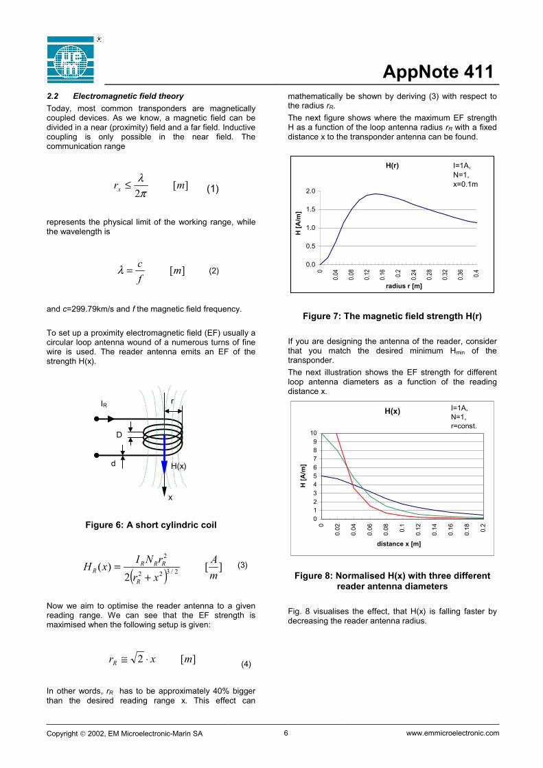
To set up a proximity electromagnetic field (EF) usually acircular loop antenna wound of a numerous turns of finewire is used. The reader antenna emits an EF of thestrength H(x).
Figure 6: A short cylindric coil
( ) ][2
)( 2/322
2
mA
xrrNIxH
R
RRRR
+= (3)
Now we aim to optimise the reader antenna to a givenreading range. We can see that the EF strength ismaximised when the following setup is given:
][2 mxrR ⋅≅ (4)
In other words, rR has to be approximately 40% biggerthan the desired reading range x. This effect can
mathematically be shown by deriving (3) with respect tothe radius rR.The next figure shows where the maximum EF strengthH as a function of the loop antenna radius rR with a fixeddistance x to the transponder antenna can be found.
H(r)
0.0
0.5
1.0
1.5
2.0
0
0.04
0.08
0.12
0.16 0.2 0.24
0.28
0.32
0.36 0.4
radius r [m]H
[A/m
]
I=1A, N=1, x=0.1m
Figure 7: The magnetic field strength H(r)
If you are designing the antenna of the reader, considerthat you match the desired minimum Hmin of thetransponder.The next illustration shows the EF strength for differentloop antenna diameters as a function of the readingdistance x.
H(x)
0123456789
10
0
0.02
0.04
0.06
0.08 0.1
0.12
0.14
0.16
0.18 0.2
distance x [m]
H [A
/m]
I=1A, N=1,r=const.
Figure 8: Normalised H(x) with three differentreader antenna diameters
Fig. 8 visualises the effect, that H(x) is falling faster bydecreasing the reader antenna radius.
D
d H(x)
x
IR r

AppNote 411
Copyright 2002, EM Microelectronic-Marin SA 7 www.emmicroelectronic.com
2.3 Magnetic field and inductivityThis chapter describes the calculation of the inductivity Lof a certain antenna. The inductivity is basically a pureissue of material and geometry.By using Biot-Savart the flux density B is given by
( ) ][2
)( 22/322
2
TmVs
xrrNIHxB
R
RRRR =
+
⋅=⋅=
µµ (5)
Knowing that the magnetic flux is
][VsABNIL ⋅=⋅=Φ (6)
We aim to isolate the inductivity L. For most RFIDapplications a circular reader coil will be used andtherefore the simple formula, where the factor 1.9 informula (7) is given by experience [B2]:
][ln0
9.10 H
AVs
rrrNL =
⋅⋅⋅= µ (7)
7.020 <<rr
(8)
The magnetic field constant is
][104 70 Am
Vs−⋅⋅= πµ (9)
For RFID applications the reader antenna inductivity L isusually in the range of 350µH... 800µH. These values fitwell for with transponders using flat circular or square aircoils, such as credit card and access applications.Other forms of antennas exist, such as the ferrite coreantenna with a varying directional performance. Suchantennas may be required in applications likeimmobilises, where the overall tag volume must berespected to a given distance performance in a systemwith fixed geometry. An appropriate formula for suchcoils is:
l
7.020 <<rr
(9)
Where µr represents the permeability of theferromagnetic material, which is a 2'000 and more,depending on the material.As shown above, the antenna inductivity can beevaluated with practical formulas. As they are empirical,they will only give you an approximate value, whichmeans, that you have to measure the antenna and adjustthe value.
2.4 Transformer principles and magnetic couplingThis chapter aims to calculate the coupling factor k of anRFID system. The coupling factor is a major key to aproper working RFID application.As we saw before, RFID applications with passivetransponders are used in close coupling (proximity field)mode. Therefore the transformer theory will help tocalculate the necessary parameters.
Figure 9: Transformer model
( )( ) ][
][
12222
21111
VMjILjRIVVMjILjRIV
ωωωω
++=++= (11)
(12)
M is the mutual inductivity of the transformer and krepresents the magnetic coupling factor.
][( 21 HLLkM ⋅= (13)
We aim to determine k as only dependent of puregeometric parameters. We need further the inducedvoltage in a coil if entered in an EF.
r0
2r
N
d
R2R1
V1 V2L1 L2
M I2I1
AppNote 411
Copyright 2002, EM Microelectronic-Marin SA 8 www.emmicroelectronic.com
][)sin( VtABNdtdNv ⋅⋅⋅⋅⋅−=Φ= ωω
(14)
Combining (5), (9), (10), (11) and (12) we get themagnetic coupling factor between the reader and thetransponder antennas. The angle θ= 0 if both antennasare in parallel.
( ) ]1[)cos(
2/322
22
xrrr
rrkRTR
TR
+⋅⋅
⋅⋅=
θ (15)
Figure 10: Parameters influencing the couplingfactor k
The coupling factor is a major key to a proper workingRFID application. The best system performance will beachieved with k=1. Thus, studying (15) closer, we cansee, that k can be maximised by:
• Minimising θ between both antennas. If thetransponder is moving and has not a fixed positionlike in application such as sports or animal tagging,this parameter is especially sensitive.
• Matching the sizes of the antenna areas. Thecoupling factor can be maximised if both antennashave the same area.
• Minimising the reading-distance x. As closer thetransponder to the reader is, as better is the couplingbetween the antennas.
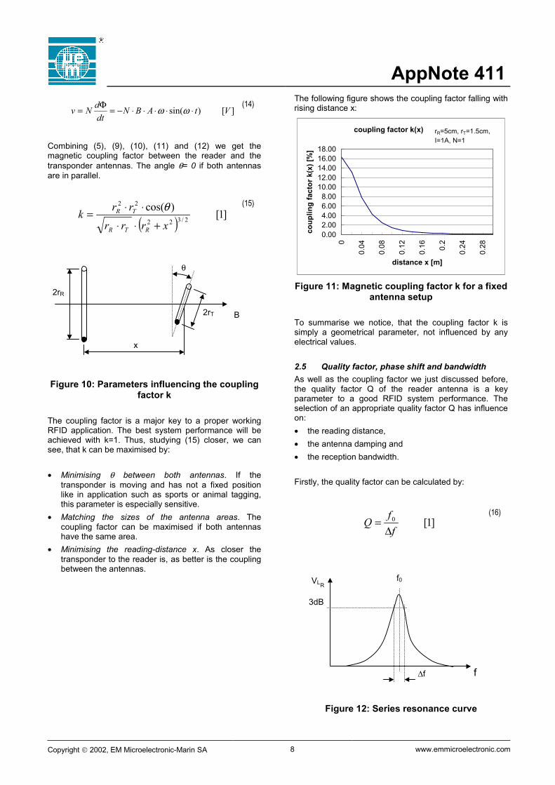
The following figure shows the coupling factor falling withrising distance x:
coupling factor k(x)
0.002.004.006.008.00
10.0012.0014.0016.0018.00
0
0.04
0.08
0.12
0.16 0.2
0.24
0.28
distance x [m]
coup
ling
fact
or k
(x) [
%]
rR=5cm, rT=1.5cm,I=1A, N=1
Figure 11: Magnetic coupling factor k for a fixedantenna setup
To summarise we notice, that the coupling factor k issimply a geometrical parameter, not influenced by anyelectrical values.
2.5 Quality factor, phase shift and bandwidthAs well as the coupling factor we just discussed before,the quality factor Q of the reader antenna is a keyparameter to a good RFID system performance. Theselection of an appropriate quality factor Q has influenceon:• the reading distance,• the antenna damping and• the reception bandwidth.
Firstly, the quality factor can be calculated by:
]1[0
ff
Q∆
=(16)
Figure 12: Series resonance curve
θ
B
x
2rT
2rR
3dB
∆f
f0VLR
f
AppNote 411
Copyright 2002, EM Microelectronic-Marin SA 9 www.emmicroelectronic.com
Secondly, the quality factor Q can also be expressed bycircuit parameters of the reader antenna setup.
]1[2 0
RL
RR R
LfQ
⋅⋅⋅=
π (17)
Furthermore the resonance voltage at the coil is:
][2 VVQV DDRL π
⋅⋅=(18)
For this reason we can measure 50V ... 100V at thereader antenna, depending on what quality factor Q andsupply voltage VDD we choose.
The following step will be, to optimise the transmissionparameters of the „transformer system“. To design the asbig as necessary, not as possible, we proceed asfollowed:
][)cos( VLLkQVVR
TTRLTL ϕ⋅⋅⋅⋅=
(19)
The minimum voltage VT desired by the transponder canbe found in the datasheet of the chosen transponder. Butit is usually limited by clamping diodes to a value ofVTmax= 18Vpp.Now as we have two independent resonant circuits,running as a series resonance (reader) and a parallelresonance (transponder) it can occur, that they are notexactly tuned to the desired frequency. Reasons maymostly be:
• Temperature effects and• Component (L, R, C) tolerances.
To imagine the influence of some percents of drift thefollowing formula was visualised [B2]:
][180)1(arctan °⋅
Ω−Ω⋅−=
πϕ RQ
(20)
][−=ΩR
T
ff
ϕ(fT): fR=125 kHz
-60.00
-40.00
-20.00
0.00
20.00
40.00
60.00
119
120
121
123
124
125
126
128
129
130
131
fT [kHz]
ϕϕ ϕϕ=
= =
=
[°]
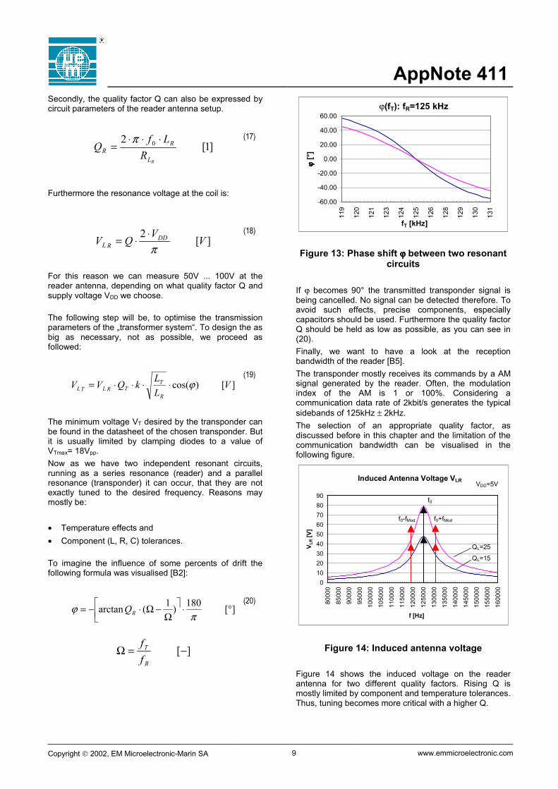
Figure 13: Phase shift ϕϕϕϕ between two resonantcircuits
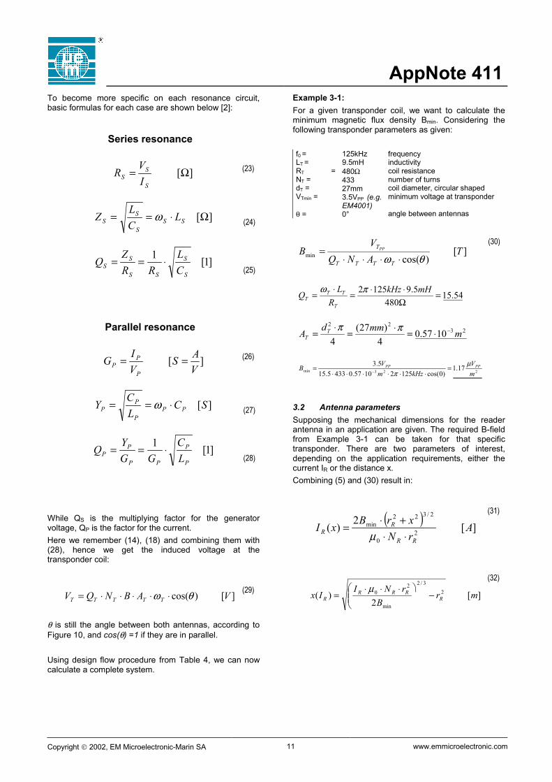
If ϕ becomes 90° the transmitted transponder signal isbeing cancelled. No signal can be detected therefore. Toavoid such effects, precise components, especiallycapacitors should be used. Furthermore the quality factorQ should be held as low as possible, as you can see in(20).Finally, we want to have a look at the receptionbandwidth of the reader [B5].The transponder mostly receives its commands by a AMsignal generated by the reader. Often, the modulationindex of the AM is 1 or 100%. Considering acommunication data rate of 2kbit/s generates the typicalsidebands of 125kHz ± 2kHz.The selection of an appropriate quality factor, asdiscussed before in this chapter and the limitation of thecommunication bandwidth can be visualised in thefollowing figure.
Induced Antenna Voltage VLR
0102030405060708090
8000
0
8500
0
9000
0
9500
0
1000
00
1050
00
1100
00
1150
00
1200
00
1250
00
1300
00
1350
00
1400
00
1450
00
1500
00
1550
00
1600
00
f [Hz]
V LR
[V]
QL=25
QL=15
VDD=5V
f0+fModf0-fMod
f0
Figure 14: Induced antenna voltage
Figure 14 shows the induced voltage on the readerantenna for two different quality factors. Rising Q ismostly limited by component and temperature tolerances.Thus, tuning becomes more critical with a higher Q.

AppNote 411
Copyright 2002, EM Microelectronic-Marin SA 10 www.emmicroelectronic.com
3 Antenna designThis chapter describes how to design your reader ortransponder antenna. Antenna coils can be configured inmany different ways. It mostly depends on the purpose ofthe applicationand theconstraintsgiven by themechanicalsetup (i.e. carimmobiliser orhandheldreader).Usually thinwire is used forantennas at125kHz, withabout 40 turns and more. For 13.56MHz often printedcircuit boards or thin film technology is used to place oneto about seven turns. At frequencies in the microwaverange, such as 2.45GHz, antennas are commonlydesigned as dipoles, according to the correspondingwavelength.Thus, although this is not quite an orthodox method, ithas some practicability. Of course there are moreappropriate ways to setup the antenna and the analogfrontend in RFID applications. Therefore the followingguidelines will help to design your system moreefficiently.As we have seen in the precedent chapters, there areseveral parameters to take in account, while designingan RFID application. We have to find a compromisebetween e.g. the quality factor QR at the reader and theinduced voltage at the transponder. Designing an RFIDapplication is a recursive procedure. Once the resonancefrequency is fixed, the following diagram can be taken asa guideline. Nevertheless it is an iterative procedure:
Step Action param.given
param. tocalculate
1 determine atransponder (e.g.EM4001). 1)
VTmin, rT, LT,NT, QT
RT
2 fix the mechanicalparameters.
rR Hmin, Bmin
3 determine the inductivityand the quality factor ofthe reader ant.
LR, QR RLR, NR
4a either you fix the max.reader current.
IR x, RR
4b or you try to maximisethe distance. rememberthe formula (4).
x IR, RR
1) Usually the transponder is a complete set of the chipand the antenna and resonance capacitor. Thereforemechanical and electrical parameters, such as theantenna diameter, the quality factor etc. are given.
Table 4: Design flow procedure
3.1 General resonant circuit parametersAs mentioned earlier, RFID data and energytransmission is based on magnetically coupledresonance circuits.
Figure 15: Series resonance circuit at thereader side
Figure 16: Parallel resonance circuit at thetransponder side
Mathematically can be shown, that in a resonance circuitwe have
]1[120 =⋅⋅ CLω (21)
and therefore the resonance frequency will be:
][2
1 10
−=⋅⋅⋅
= sHzCL
fπ
(22)
RLR
LR
CR
IR
VLR
RLT
LT CT
IT
VLT
AppNote 411
Copyright 2002, EM Microelectronic-Marin SA 11 www.emmicroelectronic.com
To become more specific on each resonance circuit,basic formulas for each case are shown below [2]:
Series resonance
][Ω=S
SS IV
R
][Ω⋅== SSS
SS L
CL
Z ω
]1[1
S
S
SS
SS C
LRR
ZQ ⋅==
(23)
(24)
(25)
Parallel resonance
][VAS
VIGP
PP ==
][SCLCY PPP
PP ⋅== ω
]1[1
P
P
PP
PP L
CGG
YQ ⋅==
(26)
(27)
(28)
While QS is the multiplying factor for the generatorvoltage, QP is the factor for the current.Here we remember (14), (18) and combining them with(28), hence we get the induced voltage at thetransponder coil:
][)cos( VABNQV TTTTT θω ⋅⋅⋅⋅⋅= (29)
θ is still the angle between both antennas, according toFigure 10, and cos(θ) =1 if they are in parallel.
Using design flow procedure from Table 4, we can nowcalculate a complete system.
Example 3-1:For a given transponder coil, we want to calculate theminimum magnetic flux density Bmin. Considering thefollowing transponder parameters as given:
f0 =LT =RT =NT =dT =VTmin =
θ =
125kHz9.5mH480Ω43327mm3.5VPP (e.g.EM4001)0°
frequencyinductivitycoil resistancenumber of turnscoil diameter, circular shapedminimum voltage at transponder
angle between antennas
][)cos(min T
ANQV
BTTTT
TPP
θω ⋅⋅⋅⋅=
54.15480
5.91252 =Ω⋅⋅=
⋅= mHkHz
RLQT
TTT
πω
2322
1057.04)27(
4mmmdA T
T−⋅=⋅=
⋅= ππ
223min 17.1)0cos(12521057.04335.15
5.3mV
kHzmVB PPPP µ
π=
⋅⋅⋅⋅⋅⋅= −
(30)
3.2 Antenna parametersSupposing the mechanical dimensions for the readerantenna in an application are given. The required B-fieldfrom Example 3-1 can be taken for that specifictransponder. There are two parameters of interest,depending on the application requirements, either thecurrent IR or the distance x.Combining (5) and (30) result in:
( )][
2)( 2
0
2/322min A
rNxrBxIRR
RR ⋅⋅
+⋅=
µ
(31)
][2
)( 23/2
min
20 mrB
rNIIx R
RRRR −
⋅⋅⋅=
µ(32)
AppNote 411
Copyright 2002, EM Microelectronic-Marin SA 12 www.emmicroelectronic.com
Example 3-2:Using the values from Example 3-1, the necessaryparameters for the reader can be calculated now:
f0 =LT =RT =NT =dT =VTmin =
θ =
VDD =rR =r0 =LR =IRP
=QR =
125kHz9.5mH480Ω43327mm3.5VPP (e.g.EM4001)0°
5V3cm0.2mm400uH100mA15
frequencyinductivitycoil resistancenumber of turnscoil diameter, circular shapedminimum voltage at transponder
angle between antennas
reader supply voltage (DC)reader antenna radiusreader antenna wire (initial value)reader antenna inductivityreader antenna current amplitudereader antenna quality factor
The number of turns of the reader coil can be calculated:
6.52
101.01030ln1030104
400
9.1/1
3
337
=
⋅⋅⋅⋅⋅⋅
=
−
−−− m
HNR
π
µ
We take NR=53.
VVVQV DDRRL 7.4751522 =⋅⋅=⋅⋅=
ππ
The coupling factor k(x) is either valuated by (15), or itcan be measured in-system as:
]1[)(T
R
R
T
LL
VVxk ⋅= (33)
As the coupling factor We consider both resonancecircuits tuned to the exact frequency, then the signalphase between both circuits will be ϕ=0 and the voltageat the transponder according to (33) and taking k=0.1:
VH
mHVVT 6.464005.91.01545 =⋅⋅⋅⋅=
µπ
Finally, the total resistance at the reader RR is being thesum of all partial resistances, such as:
• driver resistance• contact resistance at the antenna• copper resistance
Therefore the maximum current can be drawn, if [4]:
][)(
)( 2 AxkLR
VxIRRR
DDR ⋅⋅+
=ω
(34)
Calculating an RFID system is quite an iterative process.Once You have calculated a system, build it up, measureand compare these values with the calculation results.Mostly, You will spend a nice piece of time tuning yourantenna setup to assure, it will not only run on yourprototype but also in the production series. Practical tipscan be found in the next chapter.
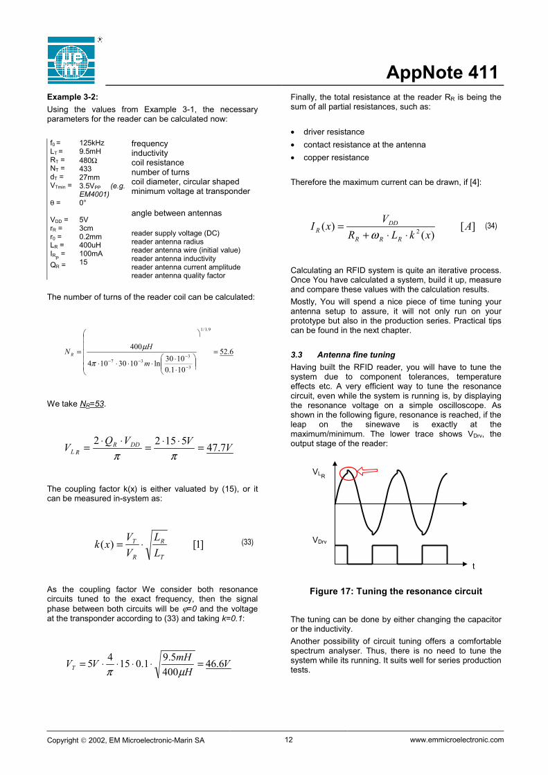
3.3 Antenna fine tuningHaving built the RFID reader, you will have to tune thesystem due to component tolerances, temperatureeffects etc. A very efficient way to tune the resonancecircuit, even while the system is running is, by displayingthe resonance voltage on a simple oscilloscope. Asshown in the following figure, resonance is reached, if theleap on the sinewave is exactly at themaximum/minimum. The lower trace shows VDrv, theoutput stage of the reader:
Figure 17: Tuning the resonance circuit
The tuning can be done by either changing the capacitoror the inductivity.Another possibility of circuit tuning offers a comfortablespectrum analyser. Thus, there is no need to tune thesystem while its running. It suits well for series productiontests.
VDrv
VLR
t
AppNote 411
Copyright 2002, EM Microelectronic-Marin SA 13 www.emmicroelectronic.com
4 Data Coding/EncodingTransmitter (Tag)The tag is responsible for ‘encoding’ i.e. inserting clocksinto the datastream according to a select coding scheme.
Receiver (Reader)Receiver is responsible for ‘decoding’ i.e. separatingclocks and data from the incoming embeddeddatastream.
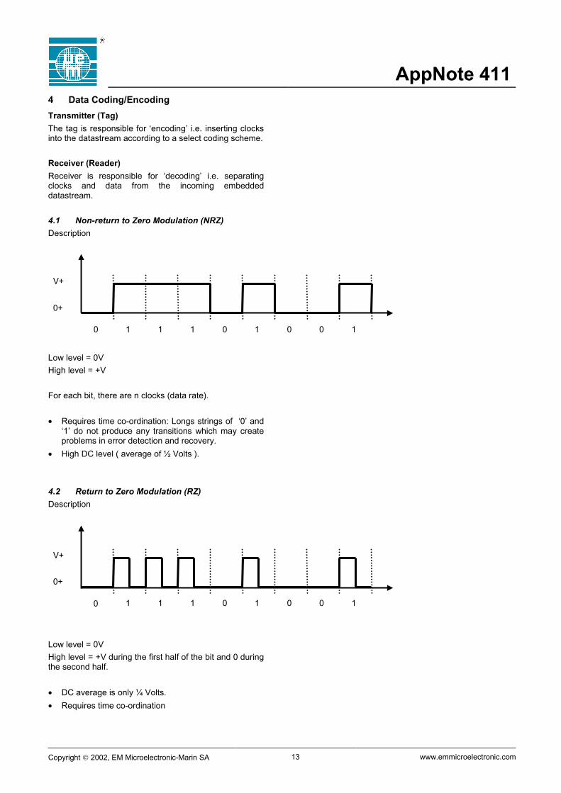
4.1 Non-return to Zero Modulation (NRZ)Description
Low level = 0VHigh level = +V
For each bit, there are n clocks (data rate).
• Requires time co-ordination: Longs strings of ‘0’ and‘1’ do not produce any transitions which may createproblems in error detection and recovery.
• High DC level ( average of ½ Volts ).
4.2 Return to Zero Modulation (RZ)Description
Low level = 0VHigh level = +V during the first half of the bit and 0 duringthe second half.
• DC average is only ¼ Volts.• Requires time co-ordination
V+
0+
111 0 11 000
V+
0+
111 0 11 000

AppNote 411
Copyright 2002, EM Microelectronic-Marin SA 14 www.emmicroelectronic.com
4.3 Manchester CodingThis code is self-clocking• There is a transition in the middle of each bit period• A 1 to 0 transition represents a '0' bit• A 0 to 1 transition represents a '1' bit
The mid-bit transition is used as clock as well as data.
• The residual DC value is eliminated by having bothpolarities for every bit
• The bandwidth required could be twice the bit rate(Efficiency of this code can be as low as 50%)
4.3.1 Differential Manchester CodingThis code is self-clocking• There is a transition in the middle of each bit period• A transition at the start of the bit period represents a
'0' bitNo transition at the start of the bit period represents a '1'bit
The mid-bit transition is used only to provide clocking.
V+
0+
111 0 11 000
V+
0+
111 0 11 000
AppNote 411
Copyright 2002, EM Microelectronic-Marin SA 15 www.emmicroelectronic.com
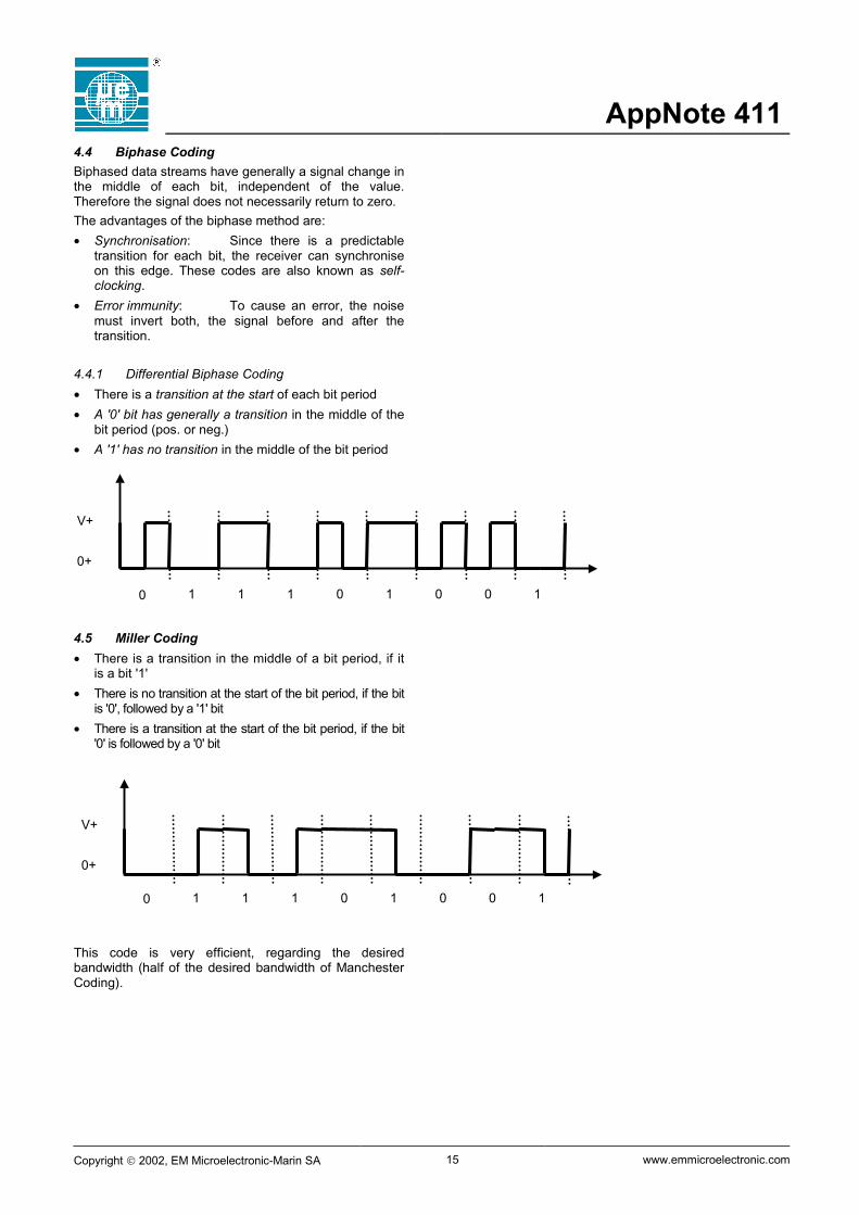
4.4 Biphase CodingBiphased data streams have generally a signal change inthe middle of each bit, independent of the value.Therefore the signal does not necessarily return to zero.The advantages of the biphase method are:• Synchronisation: Since there is a predictable
transition for each bit, the receiver can synchroniseon this edge. These codes are also known as self-clocking.
• Error immunity: To cause an error, the noisemust invert both, the signal before and after thetransition.
4.4.1 Differential Biphase Coding• There is a transition at the start of each bit period• A '0' bit has generally a transition in the middle of the
bit period (pos. or neg.)• A '1' has no transition in the middle of the bit period
4.5 Miller Coding• There is a transition in the middle of a bit period, if it
is a bit '1'• There is no transition at the start of the bit period, if the bit
is '0', followed by a '1' bit• There is a transition at the start of the bit period, if the bit
'0' is followed by a '0' bit
This code is very efficient, regarding the desiredbandwidth (half of the desired bandwidth of ManchesterCoding).
V+
0+
111 0 11 000
V+
0+
111 0 11 000
AppNote 411
Copyright 2002, EM Microelectronic-Marin SA 16 www.emmicroelectronic.com
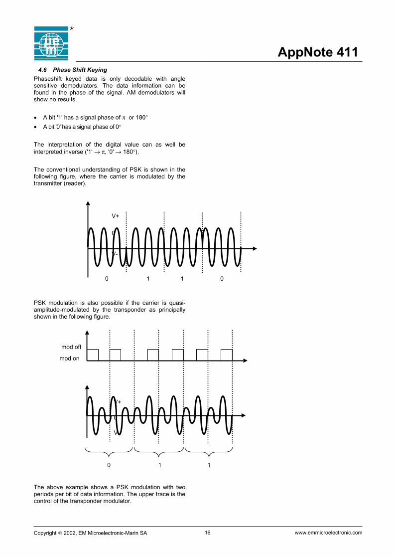
4.6 Phase Shift KeyingPhaseshift keyed data is only decodable with anglesensitive demodulators. The data information can befound in the phase of the signal. AM demodulators willshow no results.
• A bit '1' has a signal phase of π or 180°• A bit '0' has a signal phase of 0°
The interpretation of the digital value can as well beinterpreted inverse ('1' → π, '0' → 180°).
The conventional understanding of PSK is shown in thefollowing figure, where the carrier is modulated by thetransmitter (reader).
PSK modulation is also possible if the carrier is quasi-amplitude-modulated by the transponder as principallyshown in the following figure.
The above example shows a PSK modulation with twoperiods per bit of data information. The upper trace is thecontrol of the transponder modulator.
mod off
mod on
0 1 1
0 1 1 0
V+
0
V-
V+
0
V-

AppNote 411
Copyright 2002, EM Microelectronic-Marin SA 17 www.emmicroelectronic.com
5 Bibliography[B1] P. Grivet,
The Physics of Transmission Lines at High and VeryHigh Frequencies,Academic Press, London, 1970.
[B2] Karl Küpfmüller, Gerhard Kohn,Theoretische Elektrotechnik und Elektronik,Springer Verlag, Berlin, 14th edition, 1993.
[B3] Klaus Finkenzeller,RFID-Handbuch,Hanser Verlag, München, 1st edition, 1998.
[B4] Thierry Roz, Vincent Fuentes,Using low power transponders and tags for RFIDapplications,6th Wireless Symposium – February 9-12th, 1998, SantaClara, CA, USAEM Microelectronic-Marin SA, Marin.
[B5] Eberhard Herter, Wolfgang Lörcher,Nachrichtentechnik,Hanser Verlag, München, 7th edition, 1994.
[B6] W. Buesser, J. Rudin, N. Nandra, P. Goguillot, T. Roz, V.Fuentes,A Contactless Read / Write Transponder Using LowPower EEPROM Techniques,ESSCIRC 96 – September 17-19th, 1996, Neuchâtel,Switzerland,EM Microelectronic-Marin SA, Marin.
6 Glossary
Anticollision Ability of an RFID system to avoid datacollision of multiple transponders in theelectromagnetic field of a single reader.
Keying Keying means turning a transmitter onand off.
Reader device or system to read theidentification code of a Read-Onlytransponder or to program and read aRead/Write transponder.
RFID Radio Frequency Identification.
Tag Packed, embedded transponder. Alsoreferred to as data carrier, label, RFID-card, identifier.
Transponder Subassembly consisting at least of anantenna and a semiconductor,containing the desired functionality.Further components, such as capacitors,diodes etc. may be required to completethe resonant circuit or provide otherelements like voltage limitations etc.
θθθθ deg. Angle between the reader and thetransponder antenna.
µµµµr - Permeability of ferromagnetic materials.A m2 Antenna surface.B T Magnetic flux density.CR F Capacity of the reader resonance
circuit.CT F Capacity of the transponder resonance
circuit.f0 Hz Resonance frequency.GND V Power supply ground.H A/m Electromagnetic field strengthIR A Reader antenna current.IT A Transponder antenna current.k - Coupling factor of between two
antennas.LR H Reader antenna inductivity.LT H Transponder antenna inductivity.M H Mutual inductivity.NR - Number of windings of reader antenna.NT - Number of windings of transponder
antenna.QR, QS - Quality factor of the reader antenna
(series resonance).QT, QP - Quality factor of the transponder
antenna (parallel resonance).r0 m Antenna wire radius.RLR Ω Copper resistance of the reader
antenna inductivity.RLT Ω Copper resistance of the transponder
antenna inductivity.rR m Reader antenna radius.VDD V Power supply voltage at the antenna
driver.VR V Voltage at the reader resonance circuit.VT V Voltage at the transponder resonance
circuit.x m Distance between reader and
transponder antenna.µµµµ0 Magnetic field constant is µ0= 4π 10-7
A/Vs.c The speed of light in vacuum is c=
299.79 km/s.
AppNote 411
Copyright 2002, EM Microelectronic-Marin SA 18 www.emmicroelectronic.com
7 Appendix7.1 Institutes
[A1] International Telecommunication Union(ITU)Place des NationsCH-1211 Geneva 20SwitzerlandTel.: +41 22 730 51 11Fax: +41 22 733 72 56e-mail: [email protected]: http://www.iut.int
[A2] International Organization forStandardization (ISO)1, rue de VarembéCase postale 56CH-1211 Genève 20SwitzerlandTel.: + 41 22 749 01 11Fax: + 41 22 733 34 30e-mail: [email protected]: http://www.iso.ch
[A3] European Telecommunications StandardsInstitute (ETSI)ETSI Publication Office650 Route Des LuciolesF-06921 Sophia Antipolis CedexFranceTel.: +33 (0)4 92 94 49 00Fax: +33 (0)4 92 96 03 07e-mail: [email protected]: http://www.etsi.org
[A4] Federal Communications Commission(FCC)445 12th St. SWWashington DC 20554USATel.: (202) 418-0190e-mail: [email protected]: http://www.fcc.gov
7.2 Trade fairs:
[A5] SCANTECH EuropeTrade Fare for Automatic Data Capture andMobile Computinghomepage: http://www.scantech-europe.com
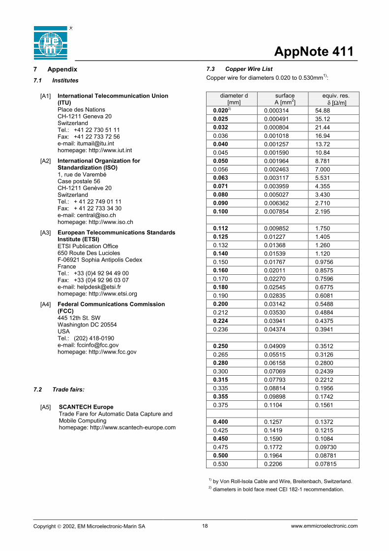
7.3 Copper Wire ListCopper wire for diameters 0.020 to 0.530mm1):
diameter d[mm]
surfaceA [mm2]
equiv. res. δ [Ω/m]
0.0202) 0.000314 54.880.025 0.000491 35.120.032 0.000804 21.440.036 0.001018 16.940.040 0.001257 13.720.045 0.001590 10.840.050 0.001964 8.7810.056 0.002463 7.0000.063 0.003117 5.5310.071 0.003959 4.3550.080 0.005027 3.4300.090 0.006362 2.7100.100 0.007854 2.195
0.112 0.009852 1.7500.125 0.01227 1.4050.132 0.01368 1.2600.140 0.01539 1.1200.150 0.01767 0.97560.160 0.02011 0.85750.170 0.02270 0.75960.180 0.02545 0.67750.190 0.02835 0.60810.200 0.03142 0.54880.212 0.03530 0.48840.224 0.03941 0.43750.236 0.04374 0.3941
0.250 0.04909 0.35120.265 0.05515 0.31260.280 0.06158 0.28000.300 0.07069 0.24390.315 0.07793 0.22120.335 0.08814 0.19560.355 0.09898 0.17420.375 0.1104 0.1561
0.400 0.1257 0.13720.425 0.1419 0.12150.450 0.1590 0.10840.475 0.1772 0.097300.500 0.1964 0.087810.530 0.2206 0.07815
1) by Von Roll-Isola Cable and Wire, Breitenbach, Switzerland.2) diameters in bold face meet CEI 182-1 recommendation.

AppNote 411
Copyright 2002, EM Microelectronic-Marin SA 19 www.emmicroelectronic.com
Notes
© EM Microelectronic-Marin SA, 09/02, Rev. D
EM Microelectronic-Marin SA cannot assume responsibility for use of any circuitry described other than circuitryentirely embodied in an EM Microelectronic-Marin SA product. EM Microelectronic-Marin SA reserves the right tochange the circuitry and specifications without notice at any time. You are strongly urged to ensure that theinformation given has not been superseded by a more up-to-date version.
Recommended