S-85S0A Series
www.ablicinc.com
5.5 V INPUT, 50 mA SYNCHRONOUS STEP-DOWNSWITCHING REGULATOR WITH 260 nA QUIESCENT CURRENT
© ABLIC Inc., 2017-2018 Rev.1.2_00
1
The S-85S0A Series introduces own distinctive low power consumption control and COT (Constant On-Time) control, features ultra low current consumption (260 nA quiescent current) and fast transient response, operates at PFM control. The S-85S0A Series realizes high efficiency in a wide range of load current consumption and provides strong support for extended period operation of mobile devices and wearable devices which are equipped with compact batteries. The S-85S0A Series can configure a step-down regulator only with a coil, an input capacitor, and an output capacitor. By using external parts recommended in this datasheet, the occupancy area can be reduced to 1.6 mm × 4.3 mm = 6.9 mm2, and it contributes to miniaturization of electronic equipment.
Features Applications
• Ultra low current consumption: 260 nA quiescent current • Wearable device • Efficiency (when under 100 μA load): 90.5% • Bluetooth device • Fast transient response: COT control • Wireless sensor network device • Input voltage: 2.2 V to 5.5 V • Healthcare equipment • Output voltage: 0.7 V to 2.5 V, in 0.05 V step • Smart meter 2.6 V to 3.9 V, in 0.1 V step • Portable game device • Output voltage accuracy: ±1.5% (1.0 V ≤ VOUT ≤ 3.9 V)
Package
• SNT-6A (1.80 mm × 1.57 mm × t0.5 mm max.)
±15 mV (0.7 V ≤ VOUT < 1.0 V) • High side power MOS FET on-resistance: 420 mΩ • Low side power MOS FET on-resistance: 320 mΩ • Soft-start function: 1 ms typ. • Under voltage lockout function (UVLO): 1.8 V typ. (detection voltage) • Thermal shutdown function: 135°C typ. (detection temperature)• Overcurrent protection function: 300 mA (at L = 2.2 μH) • Automatic recovery type short-circuit protection function:Hiccup control • Input and output capacitors: Ceramic capacitor compatible • Operation temperature range: Ta = −40°C to +85°C • Lead-free (Sn 100%), halogen-free
Typical Application Circuit
VSS
VINCIN
4.7 FPVSS VOUT
EN
SWCOUT
4.7 F
L2.2 H VOUTVIN
Efficiency
VOUT(S) = 1.8 V
[%
]
IOUT [mA]0.1 10.01 10010
0
100
80
60
40
20
VIN = 2.5 V
VIN = 3.6 V
VIN = 4.2 V

5.5 V INPUT, 50 mA SYNCHRONOUS STEP-DOWN SWITCHING REGULATOR WITH 260 nA QUIESCENT CURRENT S-85S0A Series Rev.1.2_00
2
Block Diagram
VSS
VIN
PVSS
SWL
CIN
COUT
VIN
++
−
VOUT
VOUT
EN
ON time generationcircuit
Error amplifier
Enablecircuit
UVP circuitReverse currentdetection circuit
Output control circuit
Reference voltage circuit
Soft-start cicuit
Thermal shutdown circuit
UVLO circuit
+−
+−
Overcurrent protection circuit
Figure 1

5.5 V INPUT, 50 mA SYNCHRONOUS STEP-DOWN SWITCHING REGULATOR WITH 260 nA QUIESCENT CURRENTRev.1.2_00 S-85S0A Series
3
Product Name Structure
Users can select output voltage for the S-85S0A Series. Refer to "1. Product name" regarding the contents of product name, "2. Package" regarding the package, "3. Product name list" regarding details of the product name.
1. Product name
S-85S0A B xx - I6T1 U
Package name abbreviation and packing specification*1 I6T1: SNT-6A, Tape
Environmental code U: Lead-free (Sn 100%), halogen-free
Output voltage*2, *3 07 to 39 (e.g., when the output voltage is 0.7 V, it is expressed as 07.)
*1. Refer to the tape drawing. *2. Refer to "3. Product name list". *3. In the range from 0.7 V to 2.5 V, the products which have 0.05 V step are also available. Contact our sales office when the product is necessary.
2. Package
Table 1 Package Drawing Codes
Package Name Dimension Tape Reel Land
SNT-6A PG006-A-P-SD PG006-A-C-SD PG006-A-R-SD PG006-A-L-SD

5.5 V INPUT, 50 mA SYNCHRONOUS STEP-DOWN SWITCHING REGULATOR WITH 260 nA QUIESCENT CURRENT S-85S0A Series Rev.1.2_00
4
3. Product name list
Table 2 Output Voltage (VOUT) S-85S0A Series
0.7 V ± 15 mV S-85S0AB07-I6T1U
0.8 V ± 15 mV S-85S0AB08-I6T1U
0.9 V ± 15 mV S-85S0AB09-I6T1U
1.0 V ± 1.5% S-85S0AB10-I6T1U
1.1 V ± 1.5% S-85S0AB11-I6T1U
1.2 V ± 1.5% S-85S0AB12-I6T1U
1.3 V ± 1.5% S-85S0AB13-I6T1U
1.4 V ± 1.5% S-85S0AB14-I6T1U
1.5 V ± 1.5% S-85S0AB15-I6T1U
1.6 V ± 1.5% S-85S0AB16-I6T1U
1.7 V ± 1.5% S-85S0AB17-I6T1U
1.8 V ± 1.5% S-85S0AB18-I6T1U
1.9 V ± 1.5% S-85S0AB19-I6T1U
2.0 V ± 1.5% S-85S0AB20-I6T1U
2.1 V ± 1.5% S-85S0AB21-I6T1U
2.2 V ± 1.5% S-85S0AB22-I6T1U
2.3 V ± 1.5% S-85S0AB23-I6T1U
2.4 V ± 1.5% S-85S0AB24-I6T1U
2.5 V ± 1.5% S-85S0AB25-I6T1U
2.6 V ± 1.5% S-85S0AB26-I6T1U
2.7 V ± 1.5% S-85S0AB27-I6T1U
2.8 V ± 1.5% S-85S0AB28-I6T1U
2.9 V ± 1.5% S-85S0AB29-I6T1U
3.0 V ± 1.5% S-85S0AB30-I6T1U
3.1 V ± 1.5% S-85S0AB31-I6T1U
3.2 V ± 1.5% S-85S0AB32-I6T1U
3.3 V ± 1.5% S-85S0AB33-I6T1U
3.4 V ± 1.5% S-85S0AB34-I6T1U
3.5 V ± 1.5% S-85S0AB35-I6T1U
3.6 V ± 1.5% S-85S0AB36-I6T1U
3.7 V ± 1.5% S-85S0AB37-I6T1U
3.8 V ± 1.5% S-85S0AB38-I6T1U
3.9 V ± 1.5% S-85S0AB39-I6T1U
Remark Please contact our sales office for products with specifications other than the above.

5.5 V INPUT, 50 mA SYNCHRONOUS STEP-DOWN SWITCHING REGULATOR WITH 260 nA QUIESCENT CURRENTRev.1.2_00 S-85S0A Series
5
Pin Configuration 1. SNT-6A
Table 3
54
623
1
Top view
Figure 2
Pin No. Symbol Description
1 VOUT Voltage output pin
2 VSS GND pin
3 SW External inductor connection pin
4 PVSS Power GND pin
5 VIN Power supply pin
6 EN Enable pin
"H" : Enable (normal operation) "L" : Disable (standby)

5.5 V INPUT, 50 mA SYNCHRONOUS STEP-DOWN SWITCHING REGULATOR WITH 260 nA QUIESCENT CURRENT S-85S0A Series Rev.1.2_00
6
Absolute Maximum Ratings
Table 4
(Unless otherwise specified: Ta = +25°C, VSS = 0 V)
Item Symbol Absolute Maximum Rating Unit
VIN pin voltage VIN VSS − 0.3 to VSS + 6.0 V
EN pin voltage VEN VSS − 0.3 to VIN + 0.3 ≤ VSS + 6.0 V
VOUT pin voltage VOUT VSS − 0.3 to VIN + 0.3 ≤ VSS + 6.0 V
SW pin voltage VSW VSS − 0.3 to VIN + 0.3 ≤ VSS + 6.0 V
PVSS pin voltage VPVSS VSS − 0.3 to VSS + 0.3 ≤ VSS + 6.0 V
Operation temperature Topr −40 to +85 °C
Storage temperature Tstg −40 to +125 °C
Caution The absolute maximum ratings are rated values exceeding which the product could suffer physical
damage. These values must therefore not be exceeded under any conditions.
Thermal Resistance Value
Table 5
Item Symbol Condition Min. Typ. Max. Unit
Junction-to-ambient thermal resistance*1 θJA SNT-6A
Board A − 224 − °C/W
Board B − 176 − °C/W
Board C − − − °C/W
Board D − − − °C/W
Board E − − − °C/W
*1. Test environment: compliance with JEDEC STANDARD JESD51-2A
Remark Refer to " Power Dissipation" and "Test Board" for details.

5.5 V INPUT, 50 mA SYNCHRONOUS STEP-DOWN SWITCHING REGULATOR WITH 260 nA QUIESCENT CURRENTRev.1.2_00 S-85S0A Series
7
Electrical Characteristics
Table 6
(VIN = 3.6 V*1, Ta = +25°C unless otherwise specified)
Item Symbol Condition Min. Typ. Max. Unit
Operating input voltage VIN − 2.2 3.6 5.5 V
Output voltage*2 VOUT 1.0 V ≤ VOUT ≤ 3.9 V, no external parts
VOUT(S)
× 0.985VOUT(S)
VOUT(S)
× 1.015V
0.7 V ≤ VOUT <1.0 V, no external parts VOUT(S)
− 0.015VOUT(S)
VOUT(S)
+ 0.015V
Current consumption during shutdown
ISSS VEN = 0 V − 1 100 nA
Current consumption during switching off
ISS1 VOUT = VOUT(S) + 0.1 V, VEN = VIN, no external parts, no switching operation
− 260 500 nA
High level input voltage VSH VIN = 2.2 V to 5.5 V, EN pin 1.1 − − V Low level input voltage VSL VIN = 2.2 V to 5.5 V, EN pin − − 0.3 V High level input current ISH VIN = 2.2 V to 5.5 V, EN pin, VEN = VIN −100 − 100 nA Low level input current ISL VIN = 2.2 V to 5.5 V, EN pin, VEN = 0 V −100 − 100 nA High side power MOS FET on-resistance
RHFET ISW = 100 mA − 420 − mΩ
Low side power MOS FET on-resistance
RLFET ISW = −100 mA − 320 − mΩ
High side power MOS FET leakage current
IHSW VIN = 2.2 V to 5.5 V, VEN = 0 V, VSW = 0 V − 1 100 nA
Low side power MOS FET leakage current
ILSW VIN = 2.2 V to 5.5V, VEN = 0 V, VSW = VIN −100 1 − nA
Current limit*3 ILIM L = 2.2 μH − 300 − mA
ON time*4 tON tON(S) = 1 μs × VOUT/VIN, VOUT = VOUT(S) × 0.9
tON(S)/1.3 tON(S) tON(S)/0.7 ns
Minimum OFF time tOFF(MIN) − − 100 − ns
UVLO detection voltage VUVLO− When VIN falls 1.7 1.8 1.9 V
UVLO release voltage VUVLO+ When VIN rises 1.9 2.0 2.1 V
UVP detection voltage VUVP − − VOUT(S)
× 0.7 − V
Soft-start wait time tSSW Time until VOUT starts rising − 1.5 − ms
Soft-start time tSS Time until VOUT reaches 90% after it starts rising
− 1.0 − ms
Thermal shutdown detection temperature
TSD Junction temperature − 135 − °C
Thermal shutdown release temperature
TSR Junction temperature − 115 − °C
*1. VIN = VOUT(S) + 1.0 V (VOUT(S) ≥ 2.6 V) *2. VOUT: Actual output voltage
VOUT(S): Set output voltage
*3. The current limit changes according to the L value for the inductor to be used, input voltage, and output voltage. Refer to " Operation" for details. *4. tON: Actual ON time tON(S): Set ON time

5.5 V INPUT, 50 mA SYNCHRONOUS STEP-DOWN SWITCHING REGULATOR WITH 260 nA QUIESCENT CURRENT S-85S0A Series Rev.1.2_00
8
Operation
1. Fast transient response
Distinctive COT (Constant On-Time) control is used for DC-DC converter control. The S-85S0A Series monitors the output voltage (VOUT) using a comparator and if VOUT falls below the targeted value, the high side power MOS FET will turn on for a certain amount of time. Since the high side power MOS FET turns on and VOUT rises immediately after the load current fluctuates rapidly and VOUT falls, the fast transient response is realized. The S-85S0A Series outputs ON time in proportion to VOUT and in inverse proportion to power supply voltage.
2. PFM control (pulse frequency modulation method)
The S-85S0A Series operates at PFM control and skip the pulse according to the load current. This reduces switching loss and improves efficiency. The S-85S0A Series has a built-in reverse current detection circuit. The reverse current detection circuit monitors the current flowing through the inductor. If the bottom of ripple current in the inductor falls to 0 mA, the high side power MOS FET and low side power MOS FET will turn off and switching operation will stop. Switching frequency (fSW) will fall by skipping a pulse. This means that the smaller IOUT is, the more the switching frequency will drop, and it reduces switching loss. If the power supply voltage decreases and then the potential difference between input and output becomes smaller, the S-85S0A Series will stop skipping the pulse.
3. Ultra low current consumption
When in discontinuous mode, the S-85S0A Series reduces current consumption to 260 nA typ. by intermittently operating a control circuit and a protection circuit. If switching operation stops and a certain amount of time elapses after the high side power MOS FET and low side power MOS FET turn off, only the necessary circuits will operate. Under voltage lockout function (UVLO), thermal shutdown function, current limit function, and automatic recovery type short-circuit protection function are prepared in the S-85S0A Series, and each protection function will carry out detection operation for a certain amount of time from when the high side power MOS FET turns on. It is thus able to realize ultra low current consumption.
4. EN pin
This pin starts and stops switching operation. When the EN pin is set to "L", the operation of all internal circuits, including the high side power MOS FET, is stopped, reducing current consumption. Current consumption increases when a voltage of 0.3 V to VIN − 0.3 V is applied to the EN pin. When not using the EN pin, connect it to the VIN pin. Since the EN pin is neither pulled down nor pulled up internally, do not use it in the floating status. The structure of the EN pin is shown in Figure 3.
Table 7
EN Pin Internal Circuit VOUT Pin Voltage "H" Enable (normal operation) VOUT
*1 "L" Disable (standby) "High-Z"
*1. Refer to *2 in Table 6 in " Electrical Characteristics".
VIN
VSS
EN
Figure 3

5.5 V INPUT, 50 mA SYNCHRONOUS STEP-DOWN SWITCHING REGULATOR WITH 260 nA QUIESCENT CURRENTRev.1.2_00 S-85S0A Series
9
5. Under voltage lockout function (UVLO)
The S-85S0A Series has a built-in UVLO circuit to prevent the IC from malfunctioning due to a transient status at power-on or a momentary drop in the supply voltage. When UVLO status is detected, the high side power MOS FET and low side power MOS FET will turn off, and the SW pin will change to "High-Z". For this reason, switching operation will stop. The soft-start function is reset if UVLO status is detected once, and is restarted by releasing the UVLO status. Note that the other internal circuits operate normally and the status is different from the disabled status. Also, there is a hysteresis width for avoiding malfunctions due to generation of noise etc. in the input voltage.
6. Thermal shutdown function
The S-85S0A Series has a built-in thermal shutdown circuit to limit overheating. When the junction temperature increases to 135°C typ., the thermal shutdown circuit becomes the detection status, and the switching operation is stopped. When the junction temperature decreases to 115°C typ., the thermal shutdown circuit becomes the release status, and the switching operation is restarted. If the thermal shutdown circuit becomes the detection status due to self-heating, the switching operation is stopped and output voltage (VOUT) decreases. For this reason, the self-heating is limited and the temperature of the IC decreases. The thermal shutdown circuit becomes release status when the temperature of the IC decreases, and the switching operation is restarted, thus the self-heating is generated again. Repeating this procedure makes the waveform of VOUT into a pulse-like form. Switching operation stopping and starting can be stopped by either setting the EN pin to "L", lowering the output current (IOUT) to reduce internal power consumption, or decreasing the ambient temperature.
Table 8
Thermal Shutdown Circuit VOUT Pin Voltage
Release: 115°C typ.*1 VOUT
Detection: 135°C typ.*1 "High-Z"
*1. Junction temperature
7. Overcurrent protection function
The S-85S0A Series has a built-in current limit circuit. The overcurrent protection circuit monitors the current that flows through the low side power MOS FET and limits current to prevent thermal destruction of the IC due to an overload, magnetic saturation in the inductor, etc.
When a current exceeding the current limit (ILIM) flows through the low side power MOS FET, the current limit circuit operates and prohibits turning on the high side power MOS FET until the current falls below the low side current limit (ILIMDET). If the value of the current that flows through the low side power MOS FET falls to the ILIMDET or lower, the S-85S0A Series returns to normal operation. ILIMDET is fixed at 120 mA typ. in the IC, and ILIM will vary depending on the external parts to be used. The relation between ILIM, the inductor value (L), the input voltage (VIN), and the output voltage (VOUT) are shown in the following expression.
ILIM = ILIMDET + 1
2 × L × fSW ×
(VIN − VOUT) × VOUT
VIN

5.5 V INPUT, 50 mA SYNCHRONOUS STEP-DOWN SWITCHING REGULATOR WITH 260 nA QUIESCENT CURRENT S-85S0A Series Rev.1.2_00
10
8. Automatic recovery type short-circuit protection function (Hiccup control)
The S-85S0A Series has a built-in automatic recovery type short-circuit protection function for Hiccup control. Hiccup control is a method for periodically carrying out automatic recovery when the IC detects overcurrent and stops the switching operation.
8. 1 When over load status is released
<1> Overcurrent detection <2> Under voltage protection circuit (UVP circuit) detects a drop in the output voltage (VOUT). <3> 220 μs elapse <4> Switching operation stop (for 9 ms typ.) <5> Overload status release <6> The IC restarts, soft-start function starts.
In this case, it is unnecessary to input an external reset signal for restart. <7> VOUT reaches VOUT(S) after 1.0 ms typ. elapses.
<1> <5>
<2> <4> <6>
<3> <7>
VSW
VOUT
IL*1
220 s 9.0 ms typ. 1.0 ms typ.
ILIMDET = 120 mA typ.
IOUT = 50 mA max.
0 A
0 V
0 V
VOUT(S)
VUVP typ.
Overload status Normal load status
*1. Inductor current
Figure 4
8. 2 When over load status continues
<1> Overcurrent detection <2> The UVP circuit detects a drop in VOUT. <3> 220 μs elapse <4> Switching operation stop (for 9 ms typ.) <5> The IC restarts, soft-start function starts. <6> The status returns to <2> when over load status continues after 1.25 ms typ. elapses.
<1>
<2> <4> <5> <2> <4>
<3> <3><6>
VSW
VOUT
IL*1
220 s 220 s9.0 ms typ. 9.0 ms typ.1.25 ms typ.
ILIMDET = 120 mA typ.
IOUT = 50 mA max.
0 A
0 V
0 V
VOUT(S)
VUVP typ.
Overload status
*1. Inductor current
Figure 5

5.5 V INPUT, 50 mA SYNCHRONOUS STEP-DOWN SWITCHING REGULATOR WITH 260 nA QUIESCENT CURRENTRev.1.2_00 S-85S0A Series
11
9. Pre-bias compatible soft-start function
The S-85S0A Series has a built-in pre-bias compatible soft-start circuit. If the pre-bias compatible soft-start circuit starts when electrical charge remains in the output voltage (VOUT) as a result of power supply restart, etc., or when VOUT is biased beforehand (pre-bias status), switching operation is stopped until the soft-start voltage exceeds the internal feedback voltage, and then VOUT is maintained. If the soft-start voltage exceeds the internal feedback voltage, switching operation will restart and VOUT will rise to the output voltage setting value (VOUT(S)). This allows VOUT(S) to be reached without lowering the pre-biased VOUT. In soft-start circuits which are not pre-bias compatible, a large current flows as a result of the discharge of the residual electric charge through the low side power MOS FET when switching operation starts, which could cause damage, however in a pre-bias compatible soft-start circuit, the IC is protected from the large current when switching operation starts, and it makes power supply design for the application circuit simpler. In the S-85S0A Series, VOUT reaches VOUT(S) gradually due to the soft-start circuit. In the following cases, rush current and VOUT overshoot are reduced.
• At power-on • When the EN pin changes from "L" to "H". • When UVLO operation is released. • When thermal shutdown is released. • At short-circuit recovery
In addition, the soft-start circuit operates under the following conditions. The soft-start circuit starts operating after "H" is input to the EN pin and the soft-start wait time (tSSW) = 1.5 ms typ. elapses. The soft-start time (tSS) is set to 1.0 ms typ.
• At power supply restart (the IC restart) • At UVLO detection (after UVLO release) • At thermal shutdown detection (after thermal shutdown release) • After Hiccup control
VEN
(tSSW) (tSS)
VOUT
VSW
Soft-start operation during pre-biasSoft-start wait time Soft-start time
Figure 6

5.5 V INPUT, 50 mA SYNCHRONOUS STEP-DOWN SWITCHING REGULATOR WITH 260 nA QUIESCENT CURRENT S-85S0A Series Rev.1.2_00
12
Typical Circuit
VSS
VIN
PVSS
SWL
2.2 μH
4.7 μF
4.7 μFCIN
COUT
VIN
++
−
VOUT
VOUT
EN
SS
ON time generationcircuit
Error amplifier
UVP circuit
Reverse currentdetection circuit
Output control circuit
Reference voltage circuit
Soft-start cicuit
Thermal shutdown circuit
UVLO cicuit
+−
+−
Overcurrent protection circuit
Figure 7 Caution The above connection diagram and constants will not guarantee successful operation. Perform
thorough evaluation using an actual application to set the constants.

5.5 V INPUT, 50 mA SYNCHRONOUS STEP-DOWN SWITCHING REGULATOR WITH 260 nA QUIESCENT CURRENTRev.1.2_00 S-85S0A Series
13
External Parts Selection Selectable values and recommended values for external parts are shown in Table 9. Use ceramic capacitors for CIN and COUT.
Table 9
Item Input Capacitor (CIN) Output Capacitor (COUT) Inductor (L)
Selectable value 2.2 μF or larger 4.7 μF to 100 μF 1.5 μH to 10 μH
Recommended value 4.7 μF 4.7 μF 2.2 μH
1. Input capacitor (CIN)
CIN can lower the power supply impedance, average the input current, improve the efficiency and noise tolerance. Select a capacitor according to the impedance of the power supply to be used. Also take into consideration the DC bias characteristics of the capacitor to be used.
2. Output capacitor (COUT)
COUT is used to smooth output voltage. If the capacitance is large, the overshoot and undershoot during load transient and output ripple voltage can be improved even more. Select a proper capacitor after the sufficient evaluation under actual conditions.
Table 10 Recommended Capacitors (CIN, COUT) List (at VOUT(S) ≤ 2.5 V)
Manufacturer Part Number CapacitanceWithstanding
Voltage Dimensions (L × W × H)
Murata Manufacturing Co., Ltd. GRM035R60J475ME15 4.7 μF 6.3 V 0.6 mm × 0.3 mm × 0.5 mm
Murata Manufacturing Co., Ltd. GRJ155R61A106ME12 10 μF 10 V 1.0 mm × 0.5 mm × 0.5 mm
TDK Corporation C1005X5R0J106M050BC 10 μF 6.3 V 1.0 mm × 0.5 mm × 0.5 mm
Table 11 Recommended Capacitors (CIN, COUT) List (at VOUT(S) > 2.5 V)
Manufacturer Part Number CapacitanceWithstanding
Voltage Dimensions (L × W × H)
Murata Manufacturing Co., Ltd. GRJ155R61A106ME12 10 μF 10 V 1.0 mm × 0.5 mm × 0.5 mm
TDK Corporation C1005X5R0J106M050BC 10 μF 6.3 V 1.0 mm × 0.5 mm × 0.5 mm
3. Inductor (L)
When selecting L, note the allowable current. If a current exceeding this allowable current flows through the inductor, magnetic saturation may occur, and there may be risks which substantially lower efficiency and damage the IC as a result of large current. Therefore, select an inductor so that peak current value (IPK), even during overcurrent detection, does not exceed the allowable current. When prioritizing the load response, select an inductor with a small L value such as 2.2 μH. When prioritizing the efficiency, select an inductor with a large L value such as 4.7 μH. IPK is calculated using the following expression.
IPK = IOUT + 1
2 × L × fSW ×
(VIN − VOUT) × VOUT
VIN
Table 12 Recommended Inductors (L) List (at VIN ≤ 4.2 V)
Manufacturer Part Number InductanceRated
Current Dimensions (L × W × H)
TAIYO YUDEN CO.,LTD. MBKK1608T2R2M 2.2 μH 520 mA 1.6 mm × 0.8 mm × 1.0 mm Murata Manufacturing Co., Ltd. DFE201210S-2R2M=P2 2.2 μH 2000 mA 2.0 mm × 1.2 mm × 1.0 mm Würth Elektronik GmbH & Co. KG 74438313022 2.2 μH 850 mA 1.6 mm × 1.6 mm × 1.0 mm TDK Corporation MLP2012S2R2MT0S1 2.2 μH 800 mA 2.0 mm × 1.25 mm × 0.85 mm
Table 13 Recommended Inductors (L) List (at VIN > 4.2 V)
Manufacturer Part Number InductanceRated
Current Dimensions (L × W × H)
Murata Manufacturing Co., Ltd. DFE201210S-2R2M=P2 2.2 μH 2000 mA 2.0 mm × 1.2 mm × 1.0 mm Würth Elektronik GmbH & Co. KG 74438313022 2.2 μH 850 mA 1.6 mm × 1.6 mm × 1.0 mm TDK Corporation MLP2012S2R2MT0S1 2.2 μH 800 mA 2.0 mm × 1.25 mm × 0.85 mm

5.5 V INPUT, 50 mA SYNCHRONOUS STEP-DOWN SWITCHING REGULATOR WITH 260 nA QUIESCENT CURRENT S-85S0A Series Rev.1.2_00
14
Board Layout Guidelines
Note the following cautions when determining the board layout for the S-85S0A Series.
• Place CIN as close to the VIN pin and the PVSS pin as possible. • Make the VIN pattern and GND pattern as wide as possible. • Place thermal vias in the GND pattern to ensure sufficient heat dissipation. • Keep thermal vias near CIN and COUT approximately 3 mm to 4 mm away from capacitor pins. • Large current flows through the SW pin. Make the wiring area of the pattern to be connected to the SW pin small to
minimize parasitic capacitance and emission noise. • Do not wire the SW pin pattern under the IC.
Total size 1.6 mm × 4.3 mm = 6.9 mm2
Figure 8 Reference Board Pattern
Caution The above pattern diagram does not guarantee successful operation. Perform thorough evaluation
using the actual application to determine the pattern.
Remark Refer to the land drawing of SNT-6A and "SNT Package User's Guide".

5.5 V INPUT, 50 mA SYNCHRONOUS STEP-DOWN SWITCHING REGULATOR WITH 260 nA QUIESCENT CURRENTRev.1.2_00 S-85S0A Series
15
Precautions
• Mount external capacitors and inductors as close as possible to the IC, and make single GND.
• Characteristic ripple voltage and spike noise occur in the IC containing switching regulators. Moreover rush current
flows at the time of a power supply injection. Because these largely depend on the inductor, the capacitor and
impedance of power supply to be used, fully check them using an actually mounted model.
• The 4.7 μF capacitor connected between the VIN pin and the VSS pin is a bypass capacitor. It stabilizes the power
supply in the IC, and thus effectively works for stable switching regulator operation. Allocate the bypass capacitor
as close to the IC as possible, prioritized over other parts.
• Although the IC contains a static electricity protection circuit, static electricity or voltage that exceeds the limit of
the protection circuit should not be applied.
• The power dissipation of the IC greatly varies depending on the size and material of the board to be connected.
Perform sufficient evaluation using an actual application before designing.
• ABLIC Inc. assumes no responsibility for the way in which this IC is used on products created using this IC or for
the specifications of that product, nor does ABLIC Inc. assume any responsibility for any infringement of patents or
copyrights by products that include this IC either in Japan or in other countries.

5.5 V INPUT, 50 mA SYNCHRONOUS STEP-DOWN SWITCHING REGULATOR WITH 260 nA QUIESCENT CURRENT S-85S0A Series Rev.1.2_00
16
Characteristics (Typical Data)
1. Example of major power supply dependence characteristics (Ta = +25°C)
1. 1 Current consumption during switching off (ISS1) vs. Input voltage (VIN)
1. 2 Current consumption during shutdown (ISSS) vs. Input voltage (VIN)
5.52.0VIN [V]
ISS
1 [nA
]
5.04.54.03.53.02.5
500
400
300
200
100
05.52.0
VIN [V]
ISS
S [n
A]
5.04.54.03.53.02.5
100
80
60
40
20
0
1. 3 Output voltage (VOUT) vs. Input voltage (VIN) VOUT(S) = 1.2 V
1. 4 Output voltage (VOUT) vs. Input voltage (VIN) VOUT(S) = 1.8 V
5.52.01.170
VIN [V]
VO
UT
[V]
5.04.54.03.53.02.5
1.2301.2201.2101.2001.1901.180
5.52.0VIN [V]
VO
UT
[V]
5.04.54.03.53.02.5
1.840
1.820
1.800
1.780
1.760
1. 5 Output voltage (VOUT) vs. Input voltage (VIN) VOUT(S) = 2.5 V
5.52.0VIN [V]
VO
UT
[V]
5.04.54.03.53.02.5
2.600
2.400
2.200
2.000
1.800
1. 6 ON time (tON) vs. Input voltage (VIN) VOUT(S) = 1.8 V
1. 7 Switching frequency (fSW) vs. Input voltage (VIN) VOUT(S) = 1.8 V
5.52.0VIN [V]
tON [
s]
5.04.54.03.53.02.5
1.0
0.8
0.6
0.4
0.2
0.05.52.0
VIN [V]
fSW
[MH
z]
5.04.54.03.53.02.5
1.4
1.2
1.0
0.8
0.6

5.5 V INPUT, 50 mA SYNCHRONOUS STEP-DOWN SWITCHING REGULATOR WITH 260 nA QUIESCENT CURRENTRev.1.2_00 S-85S0A Series
17
1. 8 Soft-start wait time (tSSW) vs. Input voltage (VIN) 1. 9 Soft-start time (tSS) vs. Input voltage (VIN)
5.52.0VIN [V]
tSS
W [m
s]
5.04.54.03.53.02.5
2.50
2.00
1.50
1.00
0.50
0.005.52.0
VIN [V]
tSS [m
s]
5.04.54.03.53.02.5
2.50
2.00
1.50
1.00
0.50
0.00
1. 10 High side power MOS FET on-resistance (RHFET)vs. Input voltage (VIN)
1. 11 Low side power MOS FET on-resistance (RLFET) vs. Input voltage (VIN)
5.52.0VIN [V]
RH
FET
[m
]
5.04.54.03.53.02.5
800700600500400300200100
05.52.0
VIN [V]
RH
FET
[m
]
5.04.54.03.53.02.5
800700600500400300200100
0
1. 12 High side power MOS FET leakage current (IHSW) vs. Input voltage (VIN)
1. 13 Low side power MOS FET leakage current (ILSW) vs. Input voltage (VIN)
5.52.0VIN [V]
IHS
W [n
A]
5.04.54.03.53.02.5
100
80
60
40
20
05.52.0
VIN [V]
ILSW
[nA
]
5.04.54.03.53.02.5
100
80
60
40
20
0
1. 14 High level input voltage (VSH) vs. Input voltage (VIN) 1. 15 Low level input voltage (VSL) vs. Input voltage (VIN)
5.52.00.0
VIN [V]
VS
H [V
]
5.04.54.03.53.02.5
1.21.00.80.60.40.2
5.52.00.0
VIN [V]
VS
L [V
]
5.04.54.03.53.02.5
1.21.00.80.60.40.2

5.5 V INPUT, 50 mA SYNCHRONOUS STEP-DOWN SWITCHING REGULATOR WITH 260 nA QUIESCENT CURRENT S-85S0A Series Rev.1.2_00
18
2. Example of major temperature characteristics (Ta = −40°C to +85°C)
2. 1 Current consumption during switching off (ISS1) vs. Temperature (Ta)
2. 2 Current consumption during shutdown (ISSS) vs. Temperature (Ta)
0
500
ISS
1 [nA
]
−40 857550250−25Ta [C]
400
300
200
100
VDD = 2.2 VVDD = 5.5 V
VDD = 3.6 V
0
200
ISS
S [n
A]
−40 857550250−25Ta [C]
150
100
50
VDD = 2.2 V
VDD = 5.5 VVDD = 3.6 V
2. 3 Output voltage (VOUT) vs. Temperature (Ta)
VOUT(S) = 1.2 V
2. 4 Output voltage (VOUT) vs. Temperature (Ta)
VOUT(S) = 1.8 V
1.170
1.230
VO
UT
[V]
−40 857550250−25Ta [C]
1.2201.2101.2001.1901.180
VDD = 2.2 VVDD = 5.5 V
VDD = 3.6 V
1.760
1.840V
OU
T [V
]
−40 857550250−25Ta [C]
1.820
1.800
1.780
VDD = 2.2 V
VDD = 5.5 V
VDD = 3.6 V
2. 5 Output voltage (VOUT) vs. Temperature (Ta)
VOUT(S) = 2.5 V
2.440
2.560
VO
UT
[V]
40 85755025025Ta [C]
2.5402.5202.5002.4802.460
VDD = 5.5 V
VDD = 3.6 V
2. 6 ON time (tON) vs. Temperature (Ta) 2. 7 Switching frequency (fSW) vs. Temperature (Ta)
0.0
1.2
tON [
s]
−40 857550250−25Ta [C]
1.00.80.60.40.2
VDD = 2.2 V
VDD = 5.5 V
VDD = 3.6 V
−40 857550250−25Ta [C]
fSW
[MH
z]
1.4
1.2
1.0
0.8
0.6VDD = 2.2 VVDD = 5.5 V
VDD = 3.6 V

5.5 V INPUT, 50 mA SYNCHRONOUS STEP-DOWN SWITCHING REGULATOR WITH 260 nA QUIESCENT CURRENTRev.1.2_00 S-85S0A Series
19
2. 8 Soft-start wait time (tSSW) vs. Temperature (Ta) 2. 9 Soft-start time (tSS) vs. Temperature (Ta)
40 85755025025Ta [C]
tSS
W [m
s]
2.50
2.00
1.50
1.00
0.50
0.00
VDD = 2.2 V
VDD = 5.5 VVDD = 3.6 V
40 85755025025Ta [C]
tSS [m
s]
2.50
2.00
1.50
1.00
0.50
0.00
VDD = 2.2 V
VDD = 5.5 V VDD = 3.6 V
2. 10 High side power MOS FET on-resistance (RHFET)vs. Temperature (Ta)
2. 11 Low side power MOS FET on-resistance (RLFET)vs. Temperature (Ta)
40 85755025025Ta [C]
RH
FET
[m
]
800700600500400300200100
0
VDD = 2.2 V
VDD = 5.5 VVDD = 3.6 V
40 85755025025Ta [C]
RLF
ET
[m
]
800700600500400300200100
0
VDD = 2.2 V
VDD = 5.5 VVDD = 3.6 V
2. 12 High side power MOS FET leakage current (IHSW) vs. Temperature (Ta)
2. 13 Low side power MOS FET leakage current (ILSW) vs. Temperature (Ta)
−40 857550250−25Ta [C]
IHS
W [n
A]
0
300250200150100
50
VDD = 5.5 VVDD = 3.6 V
VDD = 2.2 V
−40 857550250−25Ta [C]
ILSW
[nA
]
0
300250200150100
50
VDD = 5.5 V
VDD = 3.6 V
VDD = 2.2 V
2. 14 High level input voltage (VSH) vs. Temperature (Ta) 2. 15 Low level input voltage (VSL) vs. Temperature (Ta)
−40 857550250−25Ta [C]
VS
H [V
]
0.0
1.21.00.80.60.40.2
VDD = 5.5 V
VDD = 3.6 VVDD = 2.2 V
40 85755025025Ta [C]
VS
L [V
]
0.0
1.21.00.80.60.40.2 VDD = 2.2 V
VDD = 5.5 V
VDD = 3.6 V

5.5 V INPUT, 50 mA SYNCHRONOUS STEP-DOWN SWITCHING REGULATOR WITH 260 nA QUIESCENT CURRENT S-85S0A Series Rev.1.2_00
20
2. 16 UVLO detection voltage (VUVLO−) vs. Temperature (Ta) 2. 17 UVLO release voltage (VUVLO+) vs. Temperature (Ta)
40 85755025025Ta [C]
VU
VLO
[V
]
1.6
2.22.12.01.91.81.7
40 85755025025Ta [C]
VU
VLO
[V
]
1.6
2.22.12.01.91.81.7

5.5 V INPUT, 50 mA SYNCHRONOUS STEP-DOWN SWITCHING REGULATOR WITH 260 nA QUIESCENT CURRENTRev.1.2_00 S-85S0A Series
21
3. Transient response characteristics
The external parts shown in Table 14 are used in "3. Transient response characteristics".
Table 14
Element Name Constant Manufacturer Part Number
Inductor 2.2 μH Murata Manufacturing Co., Ltd. DFE201210S-2R2M=P2
Input capacitor 10 μF TDK Corporation C1005X5R0J106M050BC
Output capacitor 10 μF TDK Corporation C1005X5R0J106M050BC
3. 1 Power-on (VOUT = 1.8 V, VIN = 0 V → 3.6 V, Ta = +25°C)
3. 1. 1 IOUT = 0.1 mA 3. 1. 2 IOUT = 50 mA
5Time [ms]
43210
43210
−1−2−3−4
IL [
mA
]
1,4001,2001,0008006004002000−200
VIN
[V],
VO
UT [V
]
5Time [ms]
43210
43210
−1−2−3−4
IL [
mA
]
1,4001,2001,0008006004002000−200
VIN
[V
], V
OU
T [V
]
VOUT
IL
VIN
3. 2 Transient response characteristics of EN pin
(VOUT = 1.8 V, VIN = 3.6 V, VEN = 0 V → 3.6 V, Ta = +25°C)
3. 2. 1 IOUT = 0.1 mA 3. 2. 2 IOUT = 50 mA
5Time [ms]
43210
43210
−1−2−3−4
IL [
mA
]
1,4001,2001,0008006004002000−200
VE
N [
V],
VO
UT [V
]
VOUT
IL
VEN
5Time [ms]
43210
43210
−1−2−3−4
IL [
mA
]
1,4001,2001,0008006004002000−200
VE
N [
V],
VO
UT [V
]
VOUT
IL
VEN
3. 3 Power supply fluctuation (VOUT = 1.8 V, Ta = +25°C)
3. 3. 1 IOUT = 0.1 mA 3. 3. 2 IOUT = 50 mA
VIN = 3.6 V → 4.2 V → 3.6 V VIN = 3.6 V → 4.2 V → 3.6 V
50Time [ms]
403020100
5
4
3
2
1
VO
UT [V
]
2.10
2.00
1.90
1.80
1.70
VIN
[V]
VOUT
VIN
50Time [ms]
403020100
5
4
3
2
1
VO
UT [V
]
2.10
2.00
1.90
1.80
1.70
VIN
[V]
VOUT
VIN

5.5 V INPUT, 50 mA SYNCHRONOUS STEP-DOWN SWITCHING REGULATOR WITH 260 nA QUIESCENT CURRENT S-85S0A Series Rev.1.2_00
22
3. 4 Load fluctuation (VOUT = 1.8 V, VIN = 3.6 V, Ta = +25°C)
3. 4. 1 IOUT = 0.1 mA → 10 mA → 0.1 mA 3. 4. 2 IOUT = 0.1 mA → 50 mA → 0.1 mA
40Time [ms]
3020100
100
VO
UT [V
]
2.00
50 1.95
0 1.90
−50 1.85
−100 1.80
−150 1.75
−200 1.70
IOU
T [m
A]
VOUT
IOUT
40Time [ms]
3020100
100
VO
UT [V
]
2.00
50 1.95
0 1.90
−50 1.85
−100 1.80
−150 1.75
−200 1.70
IOU
T [m
A]
VOUT
IOUT
Reference Data
The external parts shown in Table 15 are used in " Reference Data".
Table 15
Condition Inductor (L) Input Capacitor (CIN) Output Capacitor (COUT)
<1> MBKK1608T2R2M (2.2 μH) TAIYO YUDEN CO.,LTD.
GRM035R60J475ME15 (4.7 μF)Murata Manufacturing Co., Ltd.
GRM035R60J475ME15 (4.7 μF)Murata Manufacturing Co., Ltd.
<2> DFE201210S-2R2M=P2 (2.2 μH) Murata Manufacturing Co., Ltd.
C1005X5R0J106M050BC (10 μF)TDK Corporation
C1005X5R0J106M050BC (10 μF)TDK Corporation
1. VOUT = 1.2 V (External parts: Condition<1>)
1. 1 Efficiency (η) vs. Output current (IOUT) 1. 2 Output voltage (VOUT) vs. Output current (IOUT)
η [%
]
IOUT [mA]0.01 0.1 10.001 10010
0
100
80
60
40
20
VIN = 3.6 V
VIN = 5.5 V
VO
UT [V
]
IOUT [mA]0.01 0.1 10.001 10010
1.0
1.5
1.4
1.3
1.2
1.1 VIN = 5.5 V
VIN = 3.6 V
2. VOUT = 1.8 V (External parts: Condition<1>)
2. 1 Efficiency (η) vs. Output current (IOUT) 2. 2 Output voltage (VOUT) vs. Output current (IOUT)
η [%
]
IOUT [mA]0.01 0.1 10.001 10010
0
100
80
60
40
20
VIN = 3.6 V
VIN = 5.5 V
VO
UT [V
]
IOUT [mA]0.01 0.1 10.001 10010
1.5
2.0
1.9
1.8
1.7
1.6
VIN = 5.5 V
VIN = 3.6 V

5.5 V INPUT, 50 mA SYNCHRONOUS STEP-DOWN SWITCHING REGULATOR WITH 260 nA QUIESCENT CURRENTRev.1.2_00 S-85S0A Series
23
3. VOUT = 1.2 V (External parts: Condition<2>)
3. 1 Efficiency (η) vs. Output current (IOUT) 3. 2 Output voltage (VOUT) vs. Output current (IOUT)
η [%
]
IOUT [mA]0.01 0.1 10.001 10010
0
100
80
60
40
20
VIN = 3.6 V
VIN = 5.5 V
VO
UT [V
]
IOUT [mA]0.01 0.1 10.001 10010
1.0
1.5
1.4
1.3
1.2
1.1 VIN = 3.6 V
VIN = 5.5 V
4. VOUT = 1.8 V (External parts: Condition<2>)
4. 1 Efficiency (η) vs. Output current (IOUT) 4. 2 Output voltage (VOUT) vs. Output current (IOUT)
η [%
]
IOUT [mA]0.01 0.1 10.001 10010
0
100
80
60
40
20
VIN = 3.6 V
VIN = 5.5 V
VO
UT [V
]
IOUT [mA]0.01 0.1 10.001 10010
1.5
2.0
1.9
1.8
1.7
1.6
VIN = 3.6 V
VIN = 5.5 V
5.5 V INPUT, 50 mA SYNCHRONOUS STEP-DOWN SWITCHING REGULATOR WITH 260 nA QUIESCENT CURRENT S-85S0A Series Rev.1.2_00
24
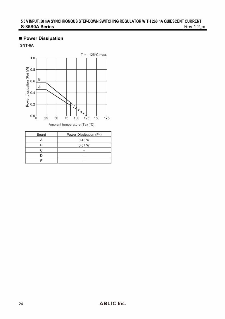
Power Dissipation
0 25 50 75 100 125 150 1750.0
0.2
0.4
0.6
0.8
1.0
Ambient temperature (Ta) [C]
Pow
er d
issi
patio
n (P
D) [
W]
Tj = 125C max.
SNT-6A
B
A
Board Power Dissipation (PD)
A 0.45 W
B 0.57 W
C −
D −
E −

(1)
1234
(2)
1234
Board B
Item Specification
Thermal via -
Material FR-4Number of copper foil layer 4
Copper foil layer [mm]
Land pattern and wiring for testing: t0.07074.2 x 74.2 x t0.03574.2 x 74.2 x t0.03574.2 x 74.2 x t0.070
Size [mm] 114.3 x 76.2 x t1.6
2
Copper foil layer [mm]
Land pattern and wiring for testing: t0.070--
74.2 x 74.2 x t0.070Thermal via -
Material FR-4
Board A
Item SpecificationSize [mm] 114.3 x 76.2 x t1.6
Number of copper foil layer
IC Mount Area
SNT-6A Test Board
No. SNT6A-A-Board-SD-1.0
ABLIC Inc.

���
�����
���
����
������ ��
��
��������������������
��������� �����
������������� �����
��������
���������
��������������
���
��� ����!
� � !
���

���
�����
���
����
������ ��
"��#�#�$�%&���
���������������
�������
'�������
���
'������������ ���������
���������
��
�������(� �����
������()$$ ��$ � �)*�
�����������(� �����
����
���
��
�
!
� �

���
�����
���
����
������ ��
�����)+�
,�����!
'�!����
-��./ -��./
0�1�
�����������2� �����
�������2� �����
��3)$4�#�#$)5��4����&6��%��&$)3�*)$&
������2��3
�7����
��

���
�����
���
����
������ ��
��
�������������)�#�2�%�����#)&���
��������� ������������������ �����
��!���
����
��!�
����
�
�
��� ��� ������� ������������������ ������������������� ���������� ����������������� ���������
������ ����������� ��������������� ���� ���������� ���������� ����������������� ��!!"����������������� ���������� ����������
"�#� �� ������������ ������$���������� �������� ������ �� ���������� ���
%�&����� ��'()��*������+���,��-����'������� ����
��� -�������������@���!�����&<*�/��� �-��!�����A��������/
!!"���
()�
����)<�)&&��&����&��&6��3)�#�*)&&�$��5�#&6�-�������������@���!�����&<*�/���������&�5�#���&6��3)�#�*)&&�$��&��&6��%��&�$��:�&6��*)%?)4���-���!�����A���������/�
��
��� -��!�����A��������/
-�������������@���!�����&<*�/

Disclaimers (Handling Precautions) 1. All the information described herein (product data, specifications, figures, tables, programs, algorithms and application
circuit examples, etc.) is current as of publishing date of this document and is subject to change without notice.
2. The circuit examples and the usages described herein are for reference only, and do not guarantee the success of any specific mass-production design. ABLIC Inc. is not responsible for damages caused by the reasons other than the products described herein (hereinafter "the products") or infringement of third-party intellectual property right and any other right due to the use of the information described herein.
3. ABLIC Inc. is not responsible for damages caused by the incorrect information described herein.
4. Be careful to use the products within their specified ranges. Pay special attention to the absolute maximum ratings, operation voltage range and electrical characteristics, etc. ABLIC Inc. is not responsible for damages caused by failures and / or accidents, etc. that occur due to the use of the products outside their specified ranges.
5. When using the products, confirm their applications, and the laws and regulations of the region or country where they are used and verify suitability, safety and other factors for the intended use.
6. When exporting the products, comply with the Foreign Exchange and Foreign Trade Act and all other export-related laws, and follow the required procedures.
7. The products must not be used or provided (exported) for the purposes of the development of weapons of mass destruction or military use. ABLIC Inc. is not responsible for any provision (export) to those whose purpose is to develop, manufacture, use or store nuclear, biological or chemical weapons, missiles, or other military use.
8. The products are not designed to be used as part of any device or equipment that may affect the human body, human life, or assets (such as medical equipment, disaster prevention systems, security systems, combustion control systems, infrastructure control systems, vehicle equipment, traffic systems, in-vehicle equipment, aviation equipment, aerospace equipment, and nuclear-related equipment), excluding when specified for in-vehicle use or other uses. Do not apply the products to the above listed devices and equipments without prior written permission by ABLIC Inc. Especially, the products cannot be used for life support devices, devices implanted in the human body and devices that directly affect human life, etc. Prior consultation with our sales office is required when considering the above uses. ABLIC Inc. is not responsible for damages caused by unauthorized or unspecified use of our products.
9. Semiconductor products may fail or malfunction with some probability. The user of the products should therefore take responsibility to give thorough consideration to safety design including redundancy, fire spread prevention measures, and malfunction prevention to prevent accidents causing injury or death, fires and social damage, etc. that may ensue from the products' failure or malfunction. The entire system must be sufficiently evaluated and applied on customer's own responsibility.
10. The products are not designed to be radiation-proof. The necessary radiation measures should be taken in the product design by the customer depending on the intended use.
11. The products do not affect human health under normal use. However, they contain chemical substances and heavy metals and should therefore not be put in the mouth. The fracture surfaces of wafers and chips may be sharp. Be careful when handling these with the bare hands to prevent injuries, etc.
12. When disposing of the products, comply with the laws and ordinances of the country or region where they are used.
13. The information described herein contains copyright information and know-how of ABLIC Inc. The information described herein does not convey any license under any intellectual property rights or any other rights belonging to ABLIC Inc. or a third party. Reproduction or copying of the information from this document or any part of this document described herein for the purpose of disclosing it to a third-party without the express permission of ABLIC Inc. is strictly prohibited.
14. For more details on the information described herein, contact our sales office.
2.0-2018.01
www.ablicinc.com
Recommended