Hardware Design with VHDL Sequential Circuit Design I ECE 443
ECE UNM 1 (11/23/09)
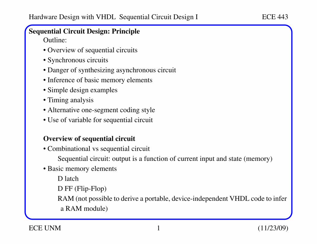
Sequential Circuit Design: Principle
Outline:
• Overview of sequential circuits
• Synchronous circuits
• Danger of synthesizing asynchronous circuit
• Inference of basic memory elements
• Simple design examples
• Timing analysis
• Alternative one-segment coding style
• Use of variable for sequential circuit
Overview of sequential circuit
• Combinational vs sequential circuit
Sequential circuit: output is a function of current input and state (memory)
• Basic memory elements
D latch
D FF (Flip-Flop)
RAM (not possible to derive a portable, device-independent VHDL code to infer
a RAM module)
Hardware Design with VHDL Sequential Circuit Design I ECE 443
ECE UNM 2 (11/23/09)
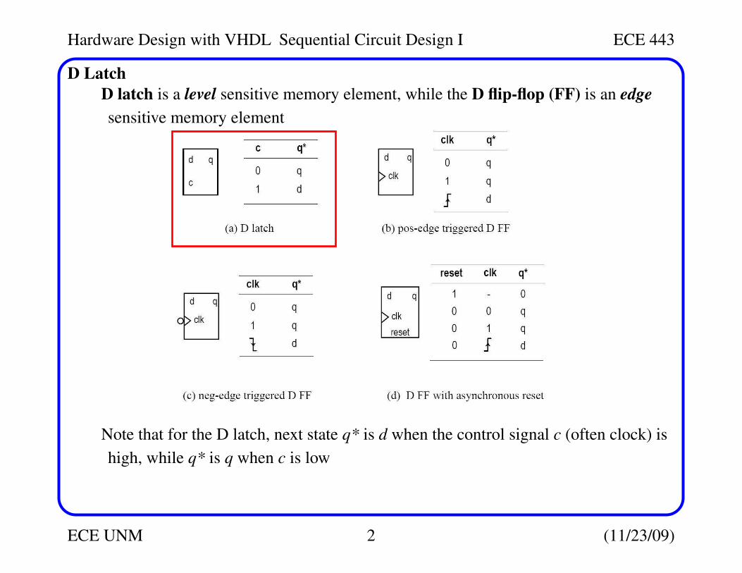
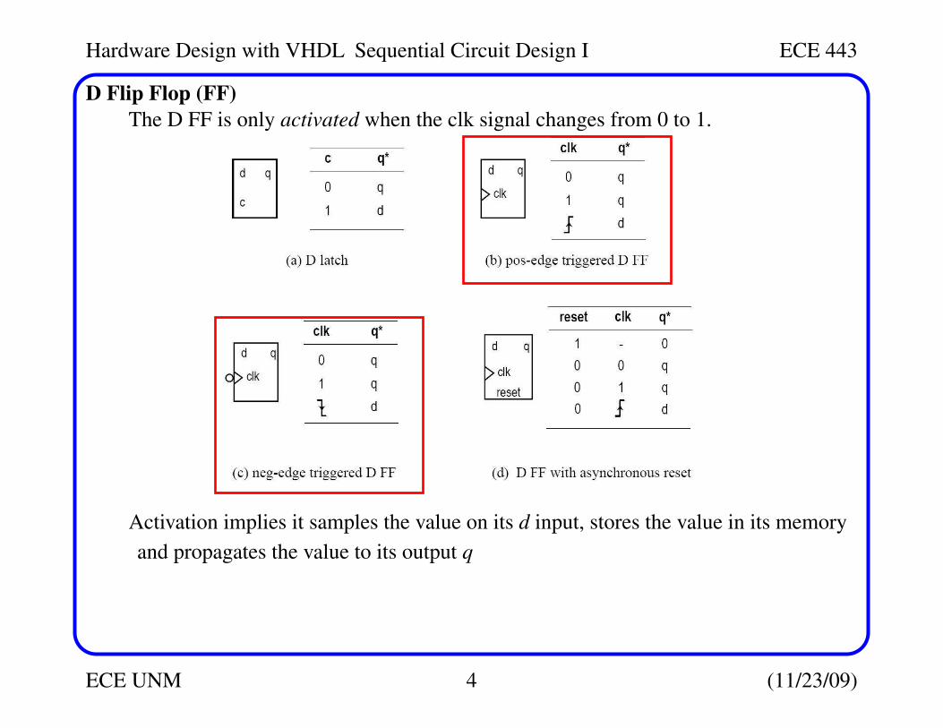
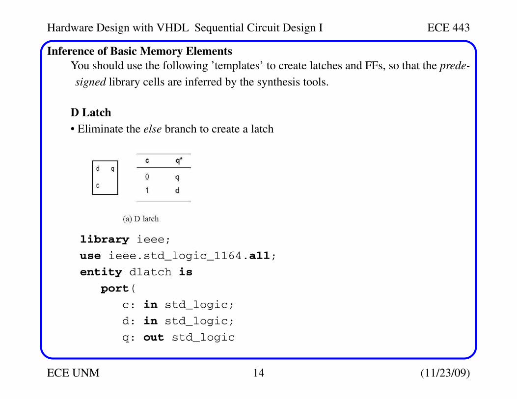
D Latch
D latch is a level sensitive memory element, while the D flip-flop (FF) is an edge
sensitive memory element
Note that for the D latch, next state q* is d when the control signal c (often clock) is
high, while q* is q when c is low
Hardware Design with VHDL Sequential Circuit Design I ECE 443
ECE UNM 3 (11/23/09)
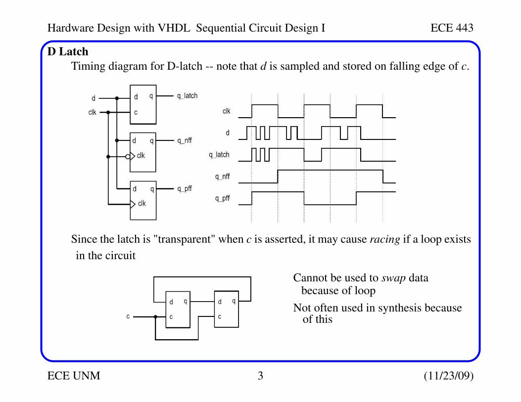
D Latch
Timing diagram for D-latch -- note that d is sampled and stored on falling edge of c.
Since the latch is "transparent" when c is asserted, it may cause racing if a loop exists
in the circuit
Cannot be used to swap databecause of loop
Not often used in synthesis becauseof this
Hardware Design with VHDL Sequential Circuit Design I ECE 443
ECE UNM 4 (11/23/09)
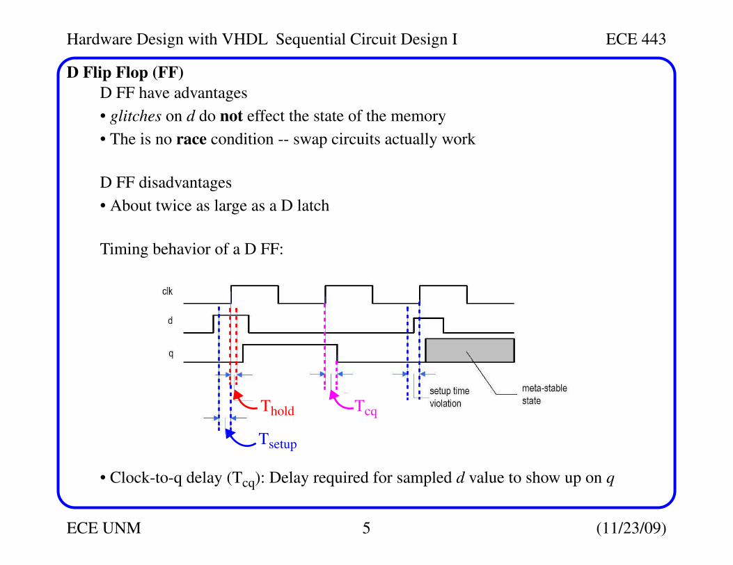
D Flip Flop (FF)
The D FF is only activated when the clk signal changes from 0 to 1.
Activation implies it samples the value on its d input, stores the value in its memory
and propagates the value to its output q
Hardware Design with VHDL Sequential Circuit Design I ECE 443
ECE UNM 5 (11/23/09)
D Flip Flop (FF)
D FF have advantages
• glitches on d do not effect the state of the memory
• The is no race condition -- swap circuits actually work
D FF disadvantages
• About twice as large as a D latch
Timing behavior of a D FF:
• Clock-to-q delay (Tcq): Delay required for sampled d value to show up on q
Thold
Tsetup
Tcq
Hardware Design with VHDL Sequential Circuit Design I ECE 443
ECE UNM 6 (11/23/09)
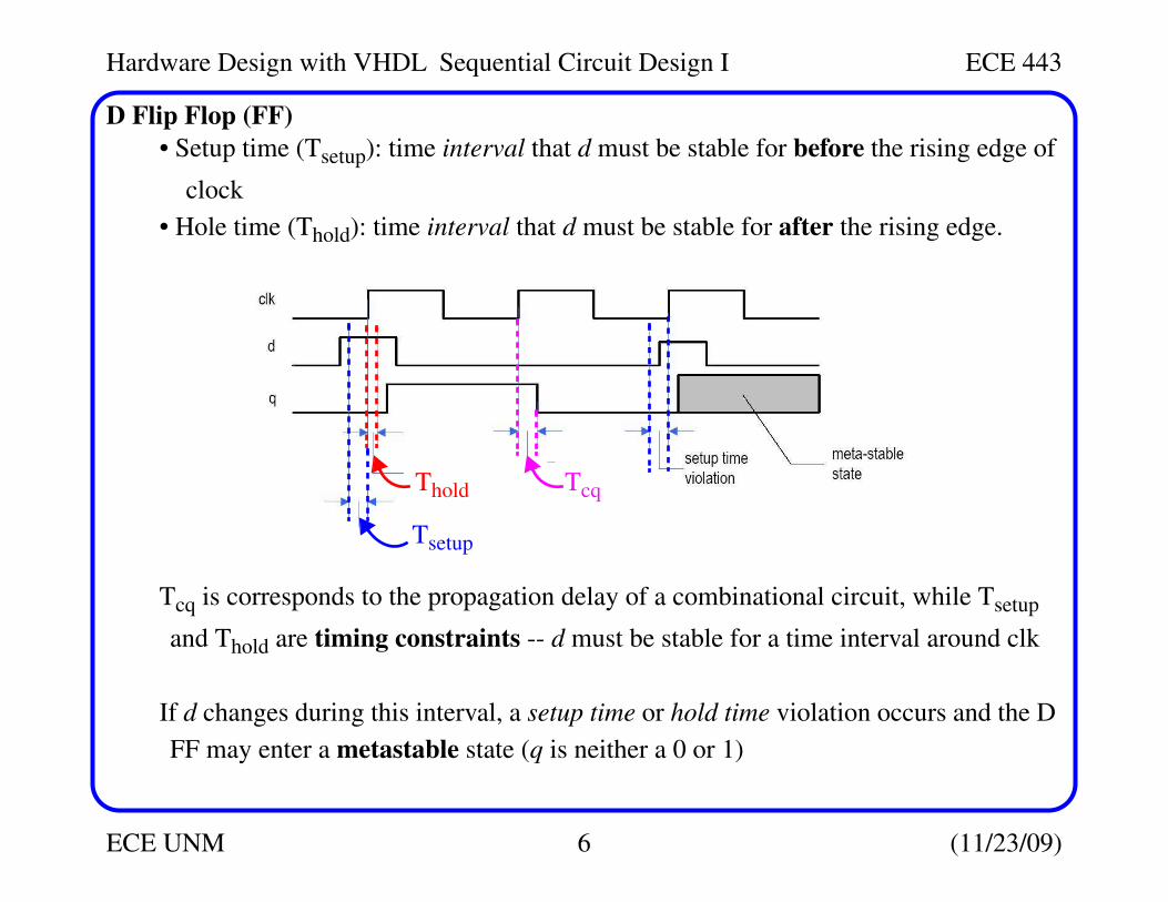
D Flip Flop (FF)
• Setup time (Tsetup): time interval that d must be stable for before the rising edge of
clock
• Hole time (Thold): time interval that d must be stable for after the rising edge.
Tcq is corresponds to the propagation delay of a combinational circuit, while Tsetup
and Thold are timing constraints -- d must be stable for a time interval around clk
If d changes during this interval, a setup time or hold time violation occurs and the D
FF may enter a metastable state (q is neither a 0 or 1)
Thold
Tsetup
Tcq
Hardware Design with VHDL Sequential Circuit Design I ECE 443
ECE UNM 7 (11/23/09)
The Clock Signal
The clock signal plays a key role in sequential circuit design
Systems can be classified according to the clock signal arrangement
Globally synchronous circuit
All memory elements (D FFs) are controlled (synchronized) by a common glo-
bal clock signal (most popular)
Globally asynchronous but locally synchronous circuit (GALS)
Used in cases in which the components of the design are spread too far apart to
allow a single synchronous clock -- a globally asynchronous circuit results
However, the smaller subsystems use a synchronous clock internally
Special interface circuits needed between subsystems to ensure proper operation
Globally asynchronous circuits
No clock is used to coordinate the memory elements
Hardware Design with VHDL Sequential Circuit Design I ECE 443
ECE UNM 8 (11/23/09)
The Clock Signal
Globally asynchronous circuits
There are two categories
• Systems that do not use the clock in a disciplined manner, for example, a ripple
counter: clock port of an FF is connected to the q output of previous FF
Poor design and not recommended
• Systems that contain ’clockless’ memory components such as the latch or a
combinational circuit with feedback loops (asynchronous circuit)
Proper design is entirely different to synchronous circuits not recommended
for HDL synthesis either
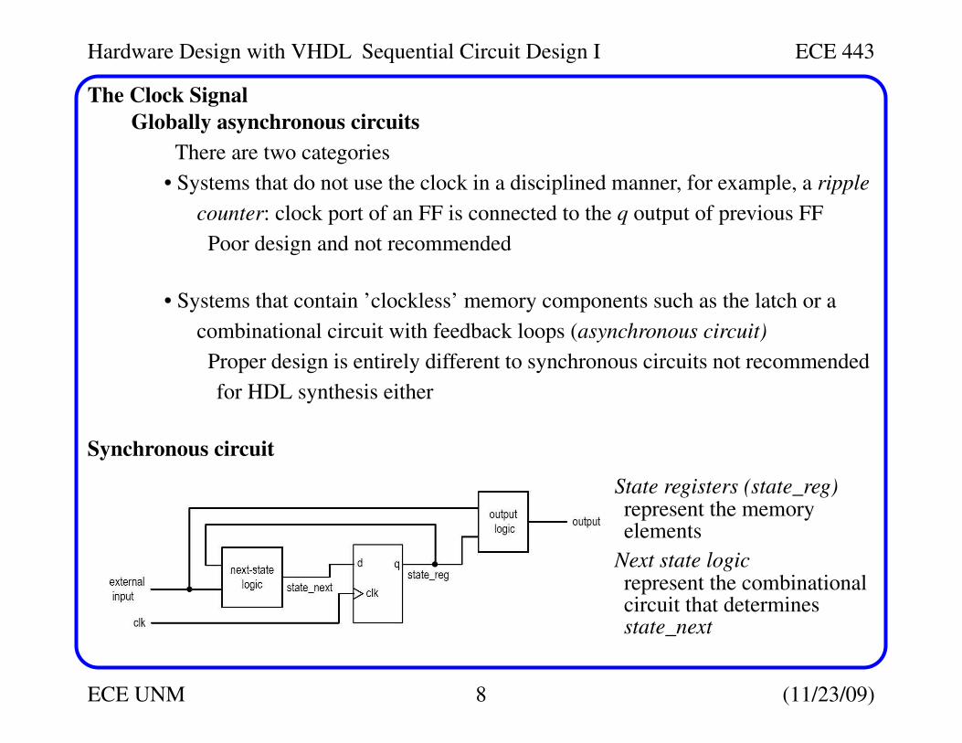
Synchronous circuit
State registers (state_reg)represent the memoryelements
Next state logicrepresent the combinationalcircuit that determinesstate_next
Hardware Design with VHDL Sequential Circuit Design I ECE 443
ECE UNM 9 (11/23/09)
Synchronous Circuits
Operation is as follows:
• At the rising edge of the clock, state_next is sampled and stored into the register
(and becomes the new value of state_reg)
• The external inputs and state_reg signals propagate through next-state and output
logic to determines the new values of the state_next and output signals
• At the rising edge of the clock, the new value of state_next is sampled and stored
and the process repeats
Note that the clock period needs to be large enough to accommodate the propagation
delay of the next-state logic, the clock-to-q delay and the setup time of the FFs
Advantages of synchronous design
• A single global clock makes the task of satisfying the timing constraints of a design
with of thousands of FFs manageable and doable
• The synchronous model separates the combinational components from the memory
elements, making it possible to treat the combinational part by itself
• Propagation delay anomalies such as hazards can be dealt with easily by focusing
on the worst case timing behavior
Hardware Design with VHDL Sequential Circuit Design I ECE 443
ECE UNM 10 (11/23/09)
Synchronous Circuits
Therefore, the synchronous model reduces a complex sequential circuit to a single
closed feedback loop and greatly simplifies the design process
Types of synchronous circuits
• Regular sequential circuit
State representation, transitions and next-state logic have a simple, regular pat-
tern, as in a incrementor or shift register
• Random sequential circuit (FSM)
More complicated state transitions and no special relationship between states
and their binary representations -- next-state logic is random
• Combined sequential circuit (FSM with a Data path, FSMD -- RTL)
Combines regular sequential circuit and an FSM, with FSM acting as control for
the sequential circuit
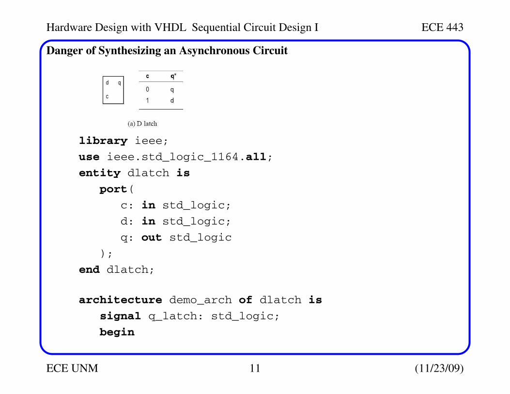
Danger of Synthesizing an Asynchronous Circuit
Consider the D Latch described earlier
We can write VHDL code as follows to represent it
Hardware Design with VHDL Sequential Circuit Design I ECE 443
ECE UNM 11 (11/23/09)
Danger of Synthesizing an Asynchronous Circuit
library ieee;
use ieee.std_logic_1164.all;
entity dlatch is
port(
c: in std_logic;
d: in std_logic;
q: out std_logic
);
end dlatch;
architecture demo_arch of dlatch is
signal q_latch: std_logic;
begin
Hardware Design with VHDL Sequential Circuit Design I ECE 443
ECE UNM 12 (11/23/09)
Danger of Synthesizing an Asynchronous Circuit
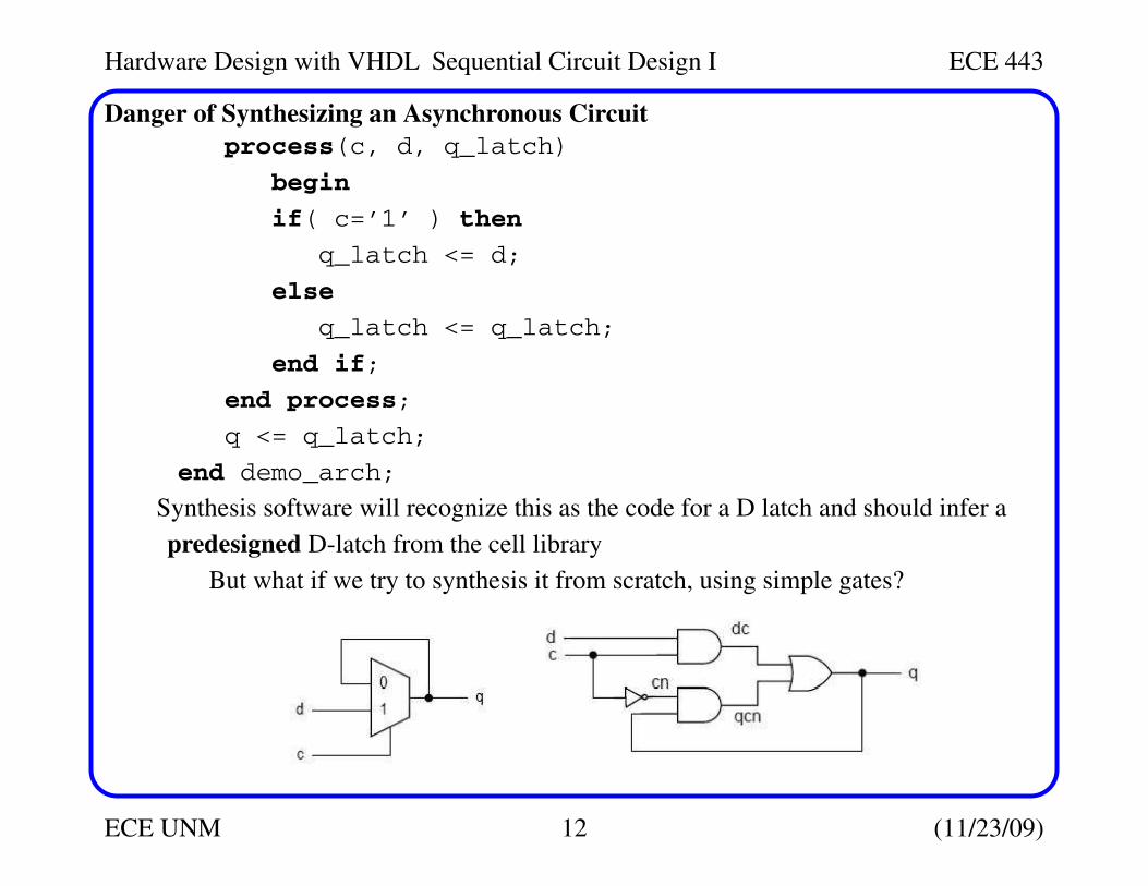
process(c, d, q_latch)
begin
if( c=’1’ ) then
q_latch <= d;
else
q_latch <= q_latch;
end if;
end process;
q <= q_latch;
end demo_arch;
Synthesis software will recognize this as the code for a D latch and should infer a
predesigned D-latch from the cell library
But what if we try to synthesis it from scratch, using simple gates?
Hardware Design with VHDL Sequential Circuit Design I ECE 443
ECE UNM 13 (11/23/09)
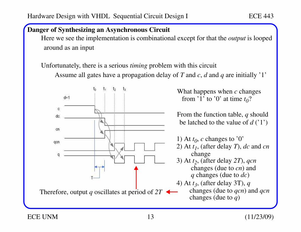
Danger of Synthesizing an Asynchronous Circuit
Here we see the implementation is combinational except for that the output is looped
around as an input
Unfortunately, there is a serious timing problem with this circuit
Assume all gates have a propagation delay of T and c, d and q are initially ’1’
What happens when c changesfrom ’1’ to ’0’ at time t0?
From the function table, q should
be latched to the value of d (’1’)
1) At t0, c changes to ’0’2) At t1, (after delay T), dc and cn
change3) At t2, (after delay 2T), qcn
changes (due to cn) and
4) At t3, (after delay 3T), qchanges (due to qcn) and qcnchanges (due to q)
q changes (due to dc)
Therefore, output q oscillates at period of 2T
Hardware Design with VHDL Sequential Circuit Design I ECE 443
ECE UNM 14 (11/23/09)
Inference of Basic Memory Elements
You should use the following ’templates’ to create latches and FFs, so that the prede-
signed library cells are inferred by the synthesis tools.
D Latch
• Eliminate the else branch to create a latch
library ieee;
use ieee.std_logic_1164.all;
entity dlatch is
port(
c: in std_logic;
d: in std_logic;
q: out std_logic
Hardware Design with VHDL Sequential Circuit Design I ECE 443
ECE UNM 15 (11/23/09)
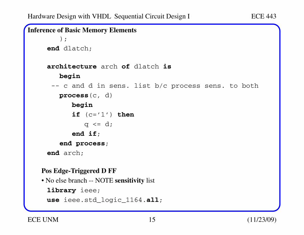
Inference of Basic Memory Elements
);
end dlatch;
architecture arch of dlatch is
begin
-- c and d in sens. list b/c process sens. to both
process(c, d)
begin
if (c=’1’) then
q <= d;
end if;
end process;
end arch;
Pos Edge-Triggered D FF
• No else branch -- NOTE sensitivity list
library ieee;
use ieee.std_logic_1164.all;
Hardware Design with VHDL Sequential Circuit Design I ECE 443
ECE UNM 16 (11/23/09)
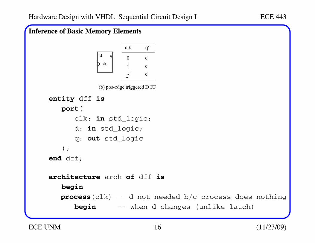
Inference of Basic Memory Elements
entity dff is
port(
clk: in std_logic;
d: in std_logic;
q: out std_logic
);
end dff;
architecture arch of dff is
begin
process(clk) -- d not needed b/c process does nothing
begin -- when d changes (unlike latch)
Hardware Design with VHDL Sequential Circuit Design I ECE 443
ECE UNM 17 (11/23/09)
Inference of Basic Memory Elements
-- ’event is true when clk changes, clk=’1’ is true when
-- NEW value of clk is ’1’ -- together means rising edge
if (clk’event and clk=’1’) then -- can also use
q <= d; -- rising_edge(clk)
end if; -- if std_logic_logic_1164 incl.
end process;
end arch;
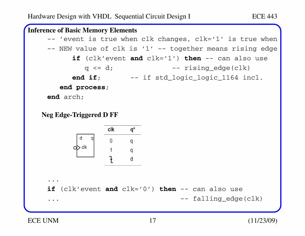
Neg Edge-Triggered D FF
...
if (clk’event and clk=’0’) then -- can also use
... -- falling_edge(clk)
Hardware Design with VHDL Sequential Circuit Design I ECE 443
ECE UNM 18 (11/23/09)
Inference of Basic Memory Elements
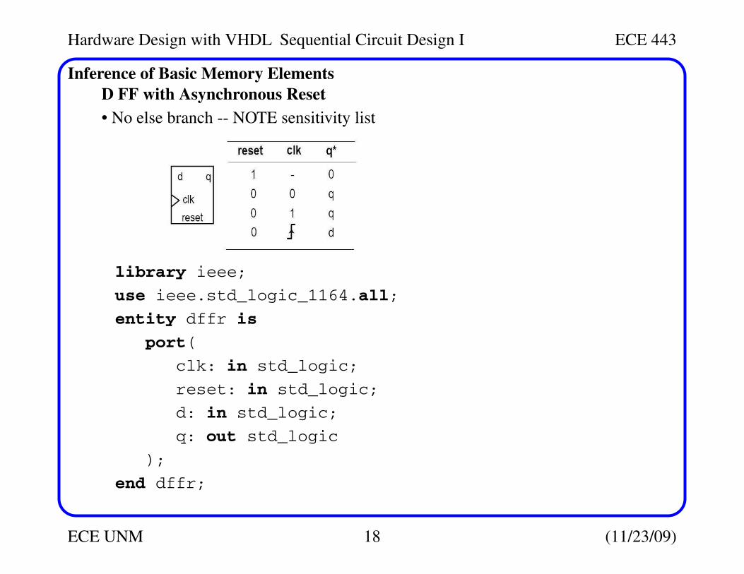
D FF with Asynchronous Reset
• No else branch -- NOTE sensitivity list
library ieee;
use ieee.std_logic_1164.all;
entity dffr is
port(
clk: in std_logic;
reset: in std_logic;
d: in std_logic;
q: out std_logic
);
end dffr;
Hardware Design with VHDL Sequential Circuit Design I ECE 443
ECE UNM 19 (11/23/09)
Inference of Basic Memory Elements
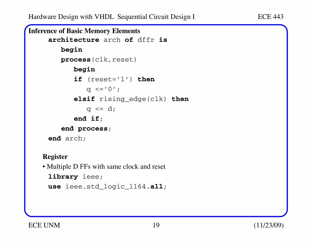
architecture arch of dffr is
begin
process(clk,reset)
begin
if (reset=’1’) then
q <=’0’;
elsif rising_edge(clk) then
q <= d;
end if;
end process;
end arch;
Register
• Multiple D FFs with same clock and reset
library ieee;
use ieee.std_logic_1164.all;
Hardware Design with VHDL Sequential Circuit Design I ECE 443
ECE UNM 20 (11/23/09)
Inference of Basic Memory Elements
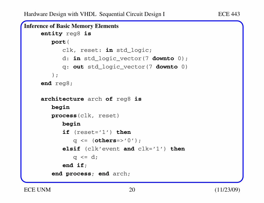
entity reg8 is
port(
clk, reset: in std_logic;
d: in std_logic_vector(7 downto 0);
q: out std_logic_vector(7 downto 0)
);
end reg8;
architecture arch of reg8 is
begin
process(clk, reset)
begin
if (reset=’1’) then
q <= (others=>’0’);
elsif (clk’event and clk=’1’) then
q <= d;
end if;
end process; end arch;
Hardware Design with VHDL Sequential Circuit Design I ECE 443
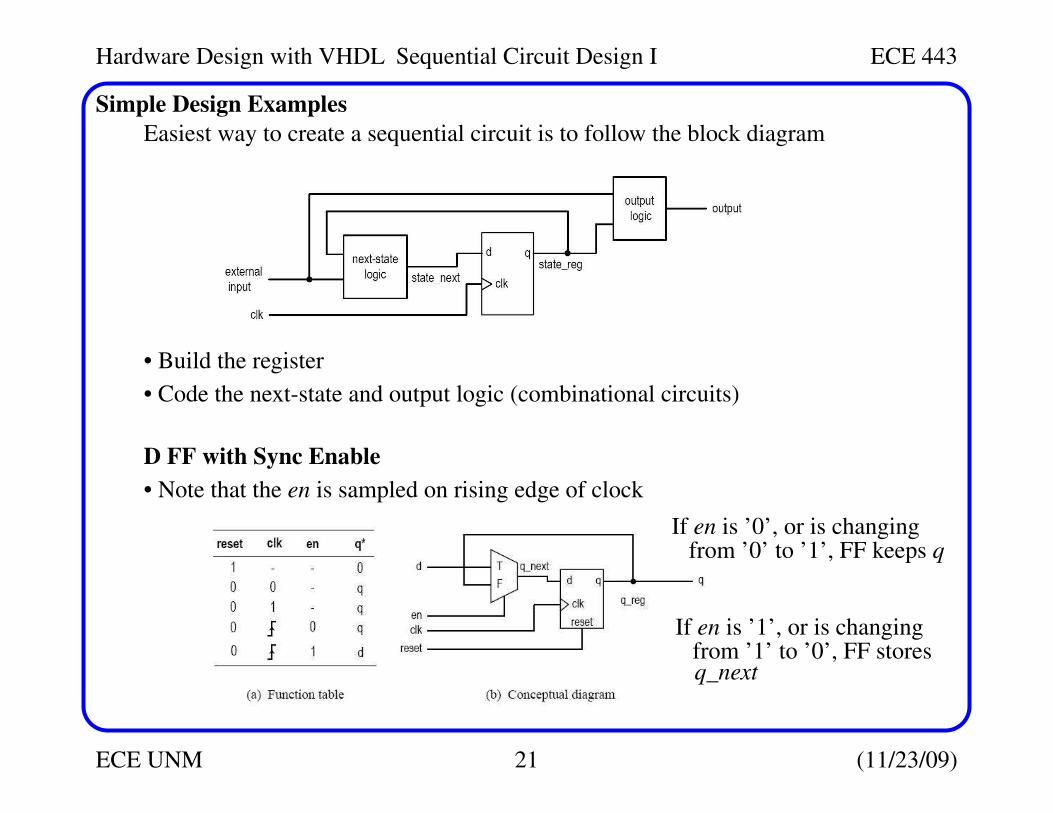
ECE UNM 21 (11/23/09)
Simple Design Examples
Easiest way to create a sequential circuit is to follow the block diagram
• Build the register
• Code the next-state and output logic (combinational circuits)
D FF with Sync Enable
• Note that the en is sampled on rising edge of clock
If en is ’0’, or is changing
If en is ’1’, or is changing
q_next
from ’0’ to ’1’, FF keeps q
from ’1’ to ’0’, FF stores
Hardware Design with VHDL Sequential Circuit Design I ECE 443
ECE UNM 22 (11/23/09)
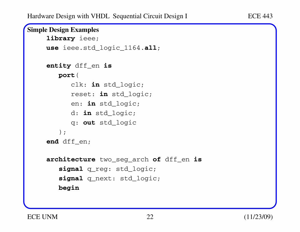
Simple Design Examples
library ieee;
use ieee.std_logic_1164.all;
entity dff_en is
port(
clk: in std_logic;
reset: in std_logic;
en: in std_logic;
d: in std_logic;
q: out std_logic
);
end dff_en;
architecture two_seg_arch of dff_en is
signal q_reg: std_logic;
signal q_next: std_logic;
begin
Hardware Design with VHDL Sequential Circuit Design I ECE 443
ECE UNM 23 (11/23/09)
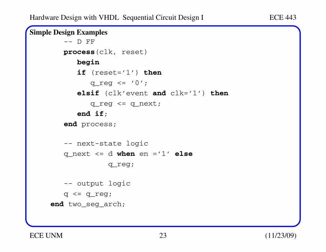
Simple Design Examples
-- D FF
process(clk, reset)
begin
if (reset=’1’) then
q_reg <= ’0’;
elsif (clk’event and clk=’1’) then
q_reg <= q_next;
end if;
end process;
-- next-state logic
q_next <= d when en =’1’ else
q_reg;
-- output logic
q <= q_reg;
end two_seg_arch;
Hardware Design with VHDL Sequential Circuit Design I ECE 443
ECE UNM 24 (11/23/09)
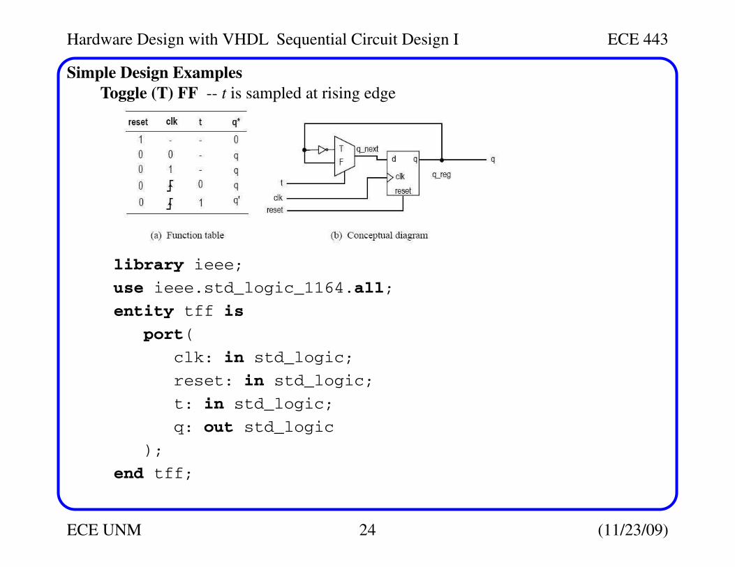
Simple Design Examples
Toggle (T) FF -- t is sampled at rising edge
library ieee;
use ieee.std_logic_1164.all;
entity tff is
port(
clk: in std_logic;
reset: in std_logic;
t: in std_logic;
q: out std_logic
);
end tff;
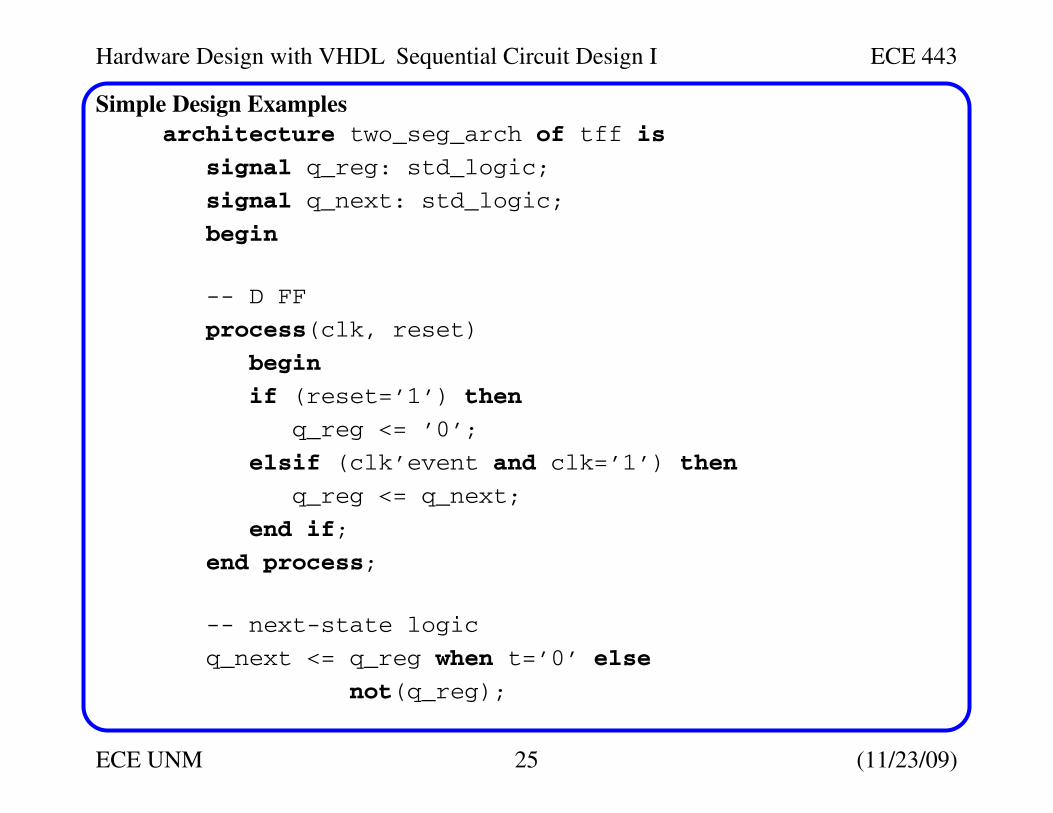
Hardware Design with VHDL Sequential Circuit Design I ECE 443
ECE UNM 25 (11/23/09)
Simple Design Examples
architecture two_seg_arch of tff is
signal q_reg: std_logic;
signal q_next: std_logic;
begin
-- D FF
process(clk, reset)
begin
if (reset=’1’) then
q_reg <= ’0’;
elsif (clk’event and clk=’1’) then
q_reg <= q_next;
end if;
end process;
-- next-state logic
q_next <= q_reg when t=’0’ else
not(q_reg);
Hardware Design with VHDL Sequential Circuit Design I ECE 443
ECE UNM 26 (11/23/09)
Simple Design Examples
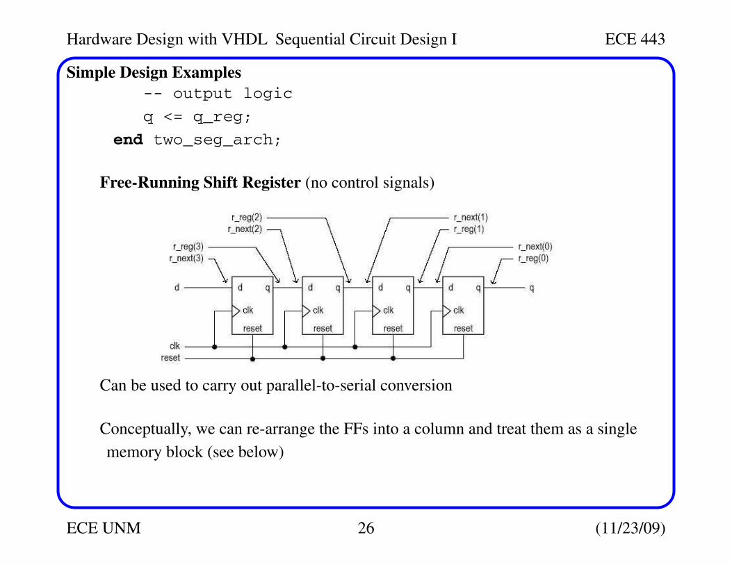
-- output logic
q <= q_reg;
end two_seg_arch;
Free-Running Shift Register (no control signals)
Can be used to carry out parallel-to-serial conversion
Conceptually, we can re-arrange the FFs into a column and treat them as a single
memory block (see below)
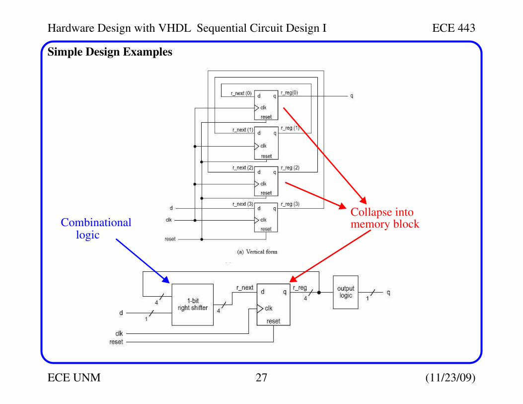
Hardware Design with VHDL Sequential Circuit Design I ECE 443
ECE UNM 27 (11/23/09)
Simple Design Examples
Collapse intomemory blockCombinational
logic
Hardware Design with VHDL Sequential Circuit Design I ECE 443
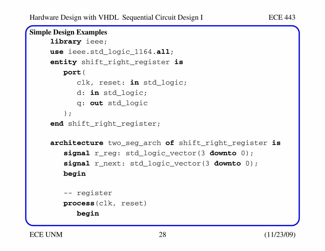
ECE UNM 28 (11/23/09)
Simple Design Examples
library ieee;
use ieee.std_logic_1164.all;
entity shift_right_register is
port(
clk, reset: in std_logic;
d: in std_logic;
q: out std_logic
);
end shift_right_register;
architecture two_seg_arch of shift_right_register is
signal r_reg: std_logic_vector(3 downto 0);
signal r_next: std_logic_vector(3 downto 0);
begin
-- register
process(clk, reset)
begin
Hardware Design with VHDL Sequential Circuit Design I ECE 443
ECE UNM 29 (11/23/09)
Simple Design Examples
if (reset=’1’) then
r_reg <= (others=>’0’);
elsif (clk’event and clk=’1’) then
r_reg <= r_next;
end if;
end process;
-- next-state logic (shift right 1 bit)
r_next <= d & r_reg(3 downto 1);
-- output
q <= r_reg(0);
end two_seg_arch;
Hardware Design with VHDL Sequential Circuit Design I ECE 443
ECE UNM 30 (11/23/09)
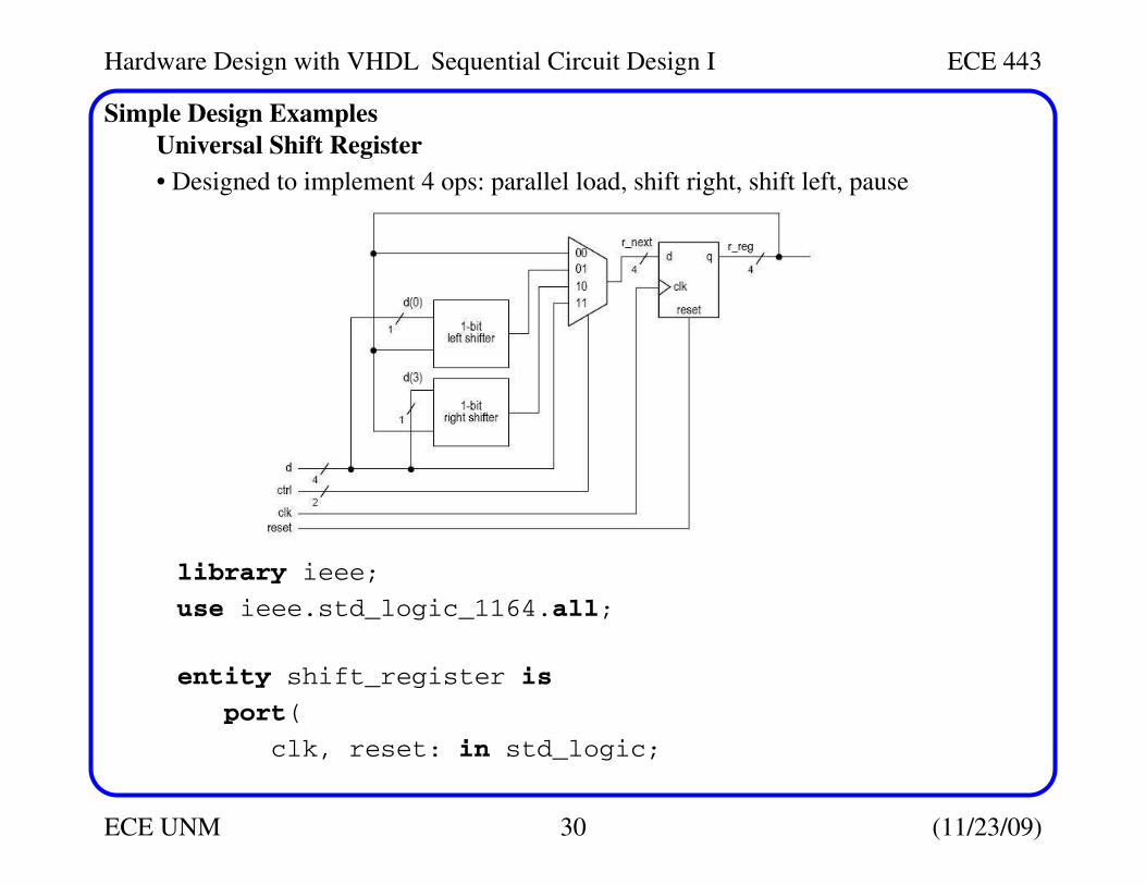
Simple Design Examples
Universal Shift Register
• Designed to implement 4 ops: parallel load, shift right, shift left, pause
library ieee;
use ieee.std_logic_1164.all;
entity shift_register is
port(
clk, reset: in std_logic;
Hardware Design with VHDL Sequential Circuit Design I ECE 443
ECE UNM 31 (11/23/09)
Simple Design Examples
ctrl: in std_logic_vector(1 downto 0);
d: in std_logic_vector(3 downto 0);
q: out std_logic_vector(3 downto 0)
);
end shift_register;
architecture two_seg_arch of shift_register is
signal r_reg: std_logic_vector(3 downto 0);
signal r_next: std_logic_vector(3 downto 0);
begin
-- register
process(clk, reset)
begin
if (reset=’1’) then
r_reg <= (others=>’0’);
elsif (clk’event and clk=’1’) then
r_reg <= r_next;
Hardware Design with VHDL Sequential Circuit Design I ECE 443
ECE UNM 32 (11/23/09)
Simple Design Examples
end if;
end process;
-- next-state logic
with ctrl select
r_next <=
r_reg when "00", -- no op
r_reg(2 downto 0) & d(0) when "01", -- sft left
d(3) & r_reg(3 downto 1) when "10", -- sft rght
d when others;
-- output
q <= r_reg;
end two_seg_arch;
Hardware Design with VHDL Sequential Circuit Design I ECE 443
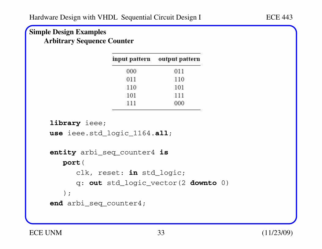
ECE UNM 33 (11/23/09)
Simple Design Examples
Arbitrary Sequence Counter
library ieee;
use ieee.std_logic_1164.all;
entity arbi_seq_counter4 is
port(
clk, reset: in std_logic;
q: out std_logic_vector(2 downto 0)
);
end arbi_seq_counter4;
Hardware Design with VHDL Sequential Circuit Design I ECE 443
ECE UNM 34 (11/23/09)
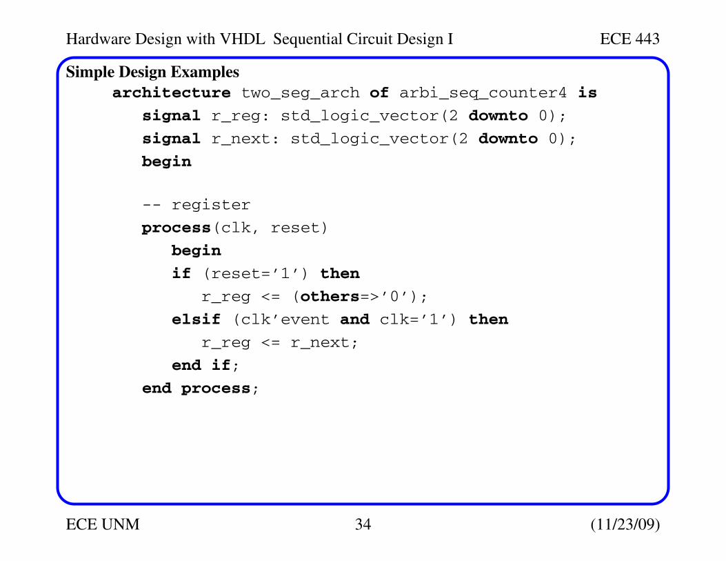
Simple Design Examples
architecture two_seg_arch of arbi_seq_counter4 is
signal r_reg: std_logic_vector(2 downto 0);
signal r_next: std_logic_vector(2 downto 0);
begin
-- register
process(clk, reset)
begin
if (reset=’1’) then
r_reg <= (others=>’0’);
elsif (clk’event and clk=’1’) then
r_reg <= r_next;
end if;
end process;
Hardware Design with VHDL Sequential Circuit Design I ECE 443
ECE UNM 35 (11/23/09)
Simple Design Examples
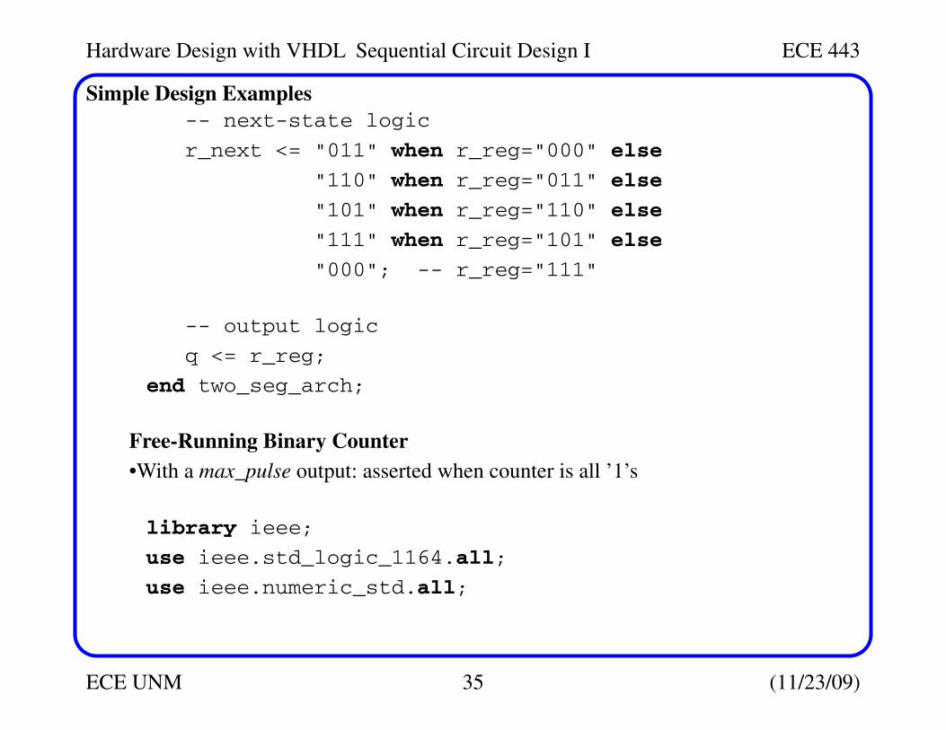
-- next-state logic
r_next <= "011" when r_reg="000" else
"110" when r_reg="011" else
"101" when r_reg="110" else
"111" when r_reg="101" else
"000"; -- r_reg="111"
-- output logic
q <= r_reg;
end two_seg_arch;
Free-Running Binary Counter
•With a max_pulse output: asserted when counter is all ’1’s
library ieee;
use ieee.std_logic_1164.all;
use ieee.numeric_std.all;
Hardware Design with VHDL Sequential Circuit Design I ECE 443
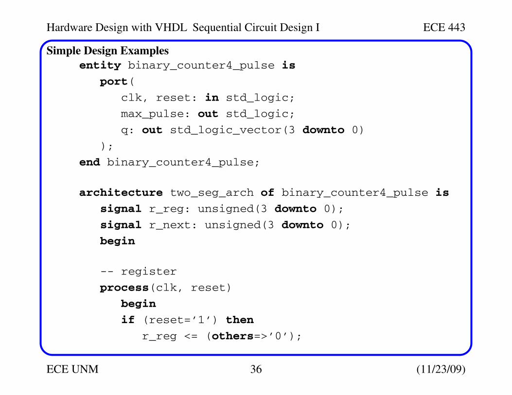
ECE UNM 36 (11/23/09)
Simple Design Examples
entity binary_counter4_pulse is
port(
clk, reset: in std_logic;
max_pulse: out std_logic;
q: out std_logic_vector(3 downto 0)
);
end binary_counter4_pulse;
architecture two_seg_arch of binary_counter4_pulse is
signal r_reg: unsigned(3 downto 0);
signal r_next: unsigned(3 downto 0);
begin
-- register
process(clk, reset)
begin
if (reset=’1’) then
r_reg <= (others=>’0’);
Hardware Design with VHDL Sequential Circuit Design I ECE 443
ECE UNM 37 (11/23/09)
Simple Design Examples
elsif (clk’event and clk=’1’) then
r_reg <= r_next;
end if;
end process;
-- next-state logic
r_next <= r_reg + 1;
-- output logic
q <= std_logic_vector(r_reg);
max_pulse <= ’1’ when (r_reg="1111") else
’0’;
end two_seg_arch;
Note that it ’wraps’ automatically
Poor practice -- may confuse some synthesis tools b/c mod op is not synthesiz-
able
r_next <= (r_reg + 1) mod 16;
Hardware Design with VHDL Sequential Circuit Design I ECE 443
ECE UNM 38 (11/23/09)
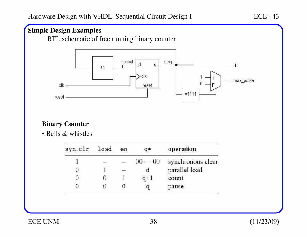
Simple Design Examples
RTL schematic of free running binary counter
Binary Counter
• Bells & whistles
Hardware Design with VHDL Sequential Circuit Design I ECE 443
ECE UNM 39 (11/23/09)
Simple Design Examples
library ieee;
use ieee.std_logic_1164.all;
use ieee.numeric_std.all;
entity binary_counter4_feature is
port(
clk, reset: in std_logic;
syn_clr, en, load: in std_logic;
d: in std_logic_vector(3 downto 0);
q: out std_logic_vector(3 downto 0)
);
end binary_counter4_feature;
architecture two_seg_arch of binary_counter4_feature is
signal r_reg: unsigned(3 downto 0);
signal r_next: unsigned(3 downto 0);
begin
Hardware Design with VHDL Sequential Circuit Design I ECE 443
ECE UNM 40 (11/23/09)
Simple Design Examples
-- register
process(clk, reset)
begin
if (reset=’1’) then
r_reg <= (others=>’0’);
elsif (clk’event and clk=’1’) then
r_reg <= r_next;
end if;
end process;
-- next-state logic
r_next <= (others=>’0’) when syn_clr=’1’ else
unsigned(d) when load=’1’ else
r_reg + 1 when en =’1’ else
r_reg;
-- output logic
q <= std_logic_vector(r_reg);
end two_seg_arch;
Hardware Design with VHDL Sequential Circuit Design I ECE 443
ECE UNM 41 (11/23/09)
Simple Design Examples
Decade (mod-10) Counter
library ieee;
use ieee.std_logic_1164.all;
use ieee.numeric_std.all;
entity mod10_counter is
port(
clk, reset: in std_logic;
q: out std_logic_vector(3 downto 0)
);
end mod10_counter;
architecture two_seg_arch of mod10_counter is
constant TEN: integer := 10;
signal r_reg: unsigned(3 downto 0);
signal r_next: unsigned(3 downto 0);
begin
-- register
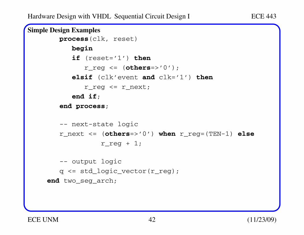
Hardware Design with VHDL Sequential Circuit Design I ECE 443
ECE UNM 42 (11/23/09)
Simple Design Examples
process(clk, reset)
begin
if (reset=’1’) then
r_reg <= (others=>’0’);
elsif (clk’event and clk=’1’) then
r_reg <= r_next;
end if;
end process;
-- next-state logic
r_next <= (others=>’0’) when r_reg=(TEN-1) else
r_reg + 1;
-- output logic
q <= std_logic_vector(r_reg);
end two_seg_arch;
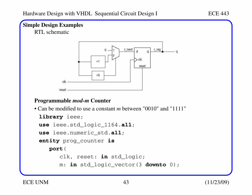
Hardware Design with VHDL Sequential Circuit Design I ECE 443
ECE UNM 43 (11/23/09)
Simple Design Examples
RTL schematic
Programmable mod-m Counter
• Can be modified to use a constant m between "0010" and "1111"
library ieee;
use ieee.std_logic_1164.all;
use ieee.numeric_std.all;
entity prog_counter is
port(
clk, reset: in std_logic;
m: in std_logic_vector(3 downto 0);
Hardware Design with VHDL Sequential Circuit Design I ECE 443
ECE UNM 44 (11/23/09)
Simple Design Examples
q: out std_logic_vector(3 downto 0)
);
end prog_counter;
architecture two_seg_clear_arch of prog_counter is
signal r_reg: unsigned(3 downto 0);
signal r_next: unsigned(3 downto 0);
begin
-- register
process(clk, reset)
begin
if (reset=’1’) then
r_reg <= (others=>’0’);
elsif (clk’event and clk=’1’) then
r_reg <= r_next;
end if;
end process;
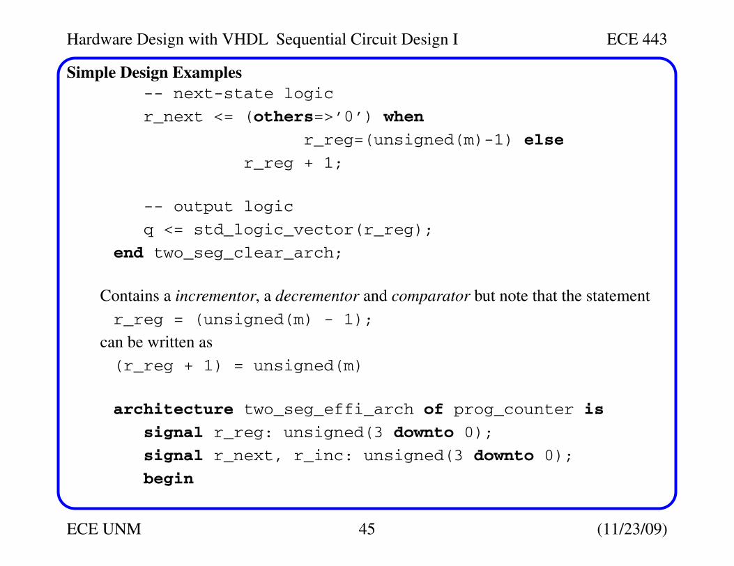
Hardware Design with VHDL Sequential Circuit Design I ECE 443
ECE UNM 45 (11/23/09)
Simple Design Examples
-- next-state logic
r_next <= (others=>’0’) when
r_reg=(unsigned(m)-1) else
r_reg + 1;
-- output logic
q <= std_logic_vector(r_reg);
end two_seg_clear_arch;
Contains a incrementor, a decrementor and comparator but note that the statement
r_reg = (unsigned(m) - 1);
can be written as
(r_reg + 1) = unsigned(m)
architecture two_seg_effi_arch of prog_counter is
signal r_reg: unsigned(3 downto 0);
signal r_next, r_inc: unsigned(3 downto 0);
begin
Hardware Design with VHDL Sequential Circuit Design I ECE 443
ECE UNM 46 (11/23/09)
Simple Design Examples
-- register
process(clk, reset)
begin
if (reset=’1’) then
r_reg <= (others=>’0’);
elsif (clk’event and clk=’1’) then
r_reg <= r_next;
end if;
end process;
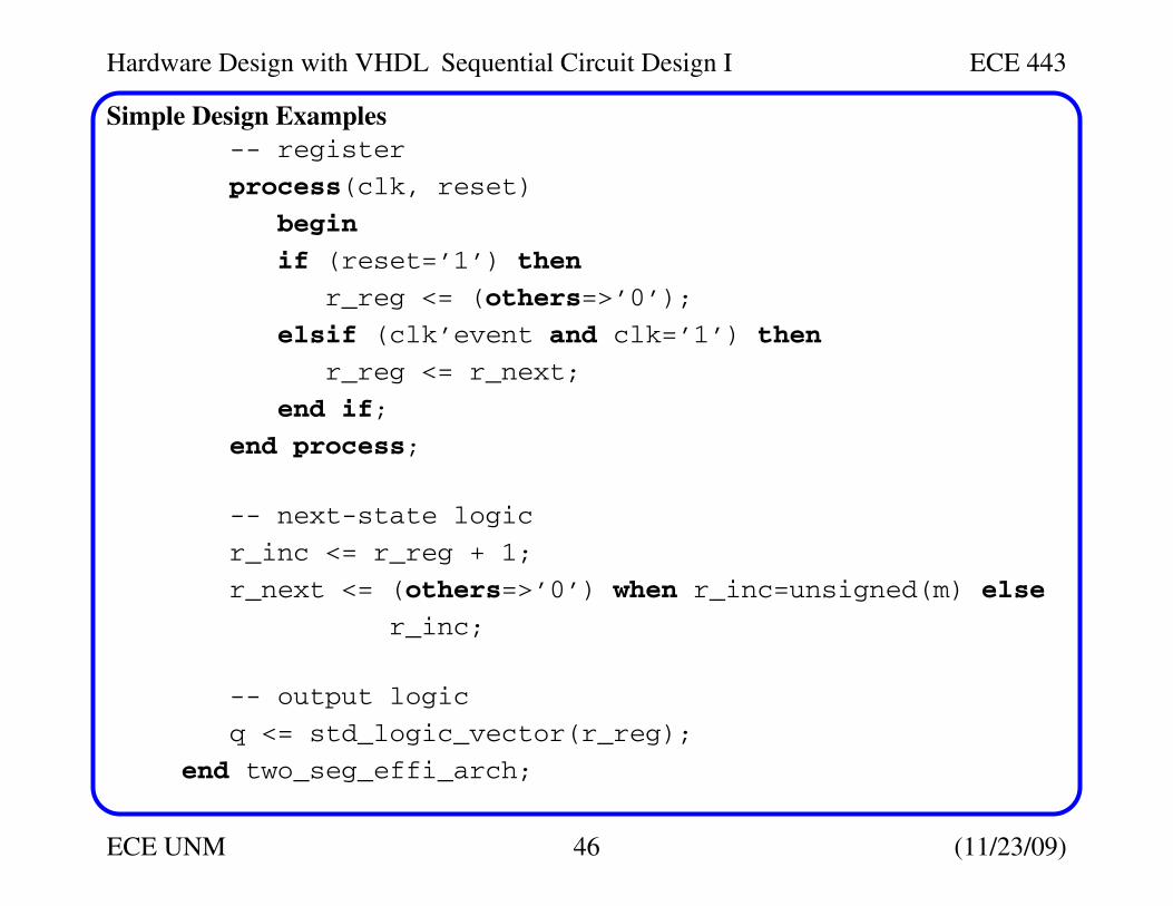
-- next-state logic
r_inc <= r_reg + 1;
r_next <= (others=>’0’) when r_inc=unsigned(m) else
r_inc;
-- output logic
q <= std_logic_vector(r_reg);
end two_seg_effi_arch;
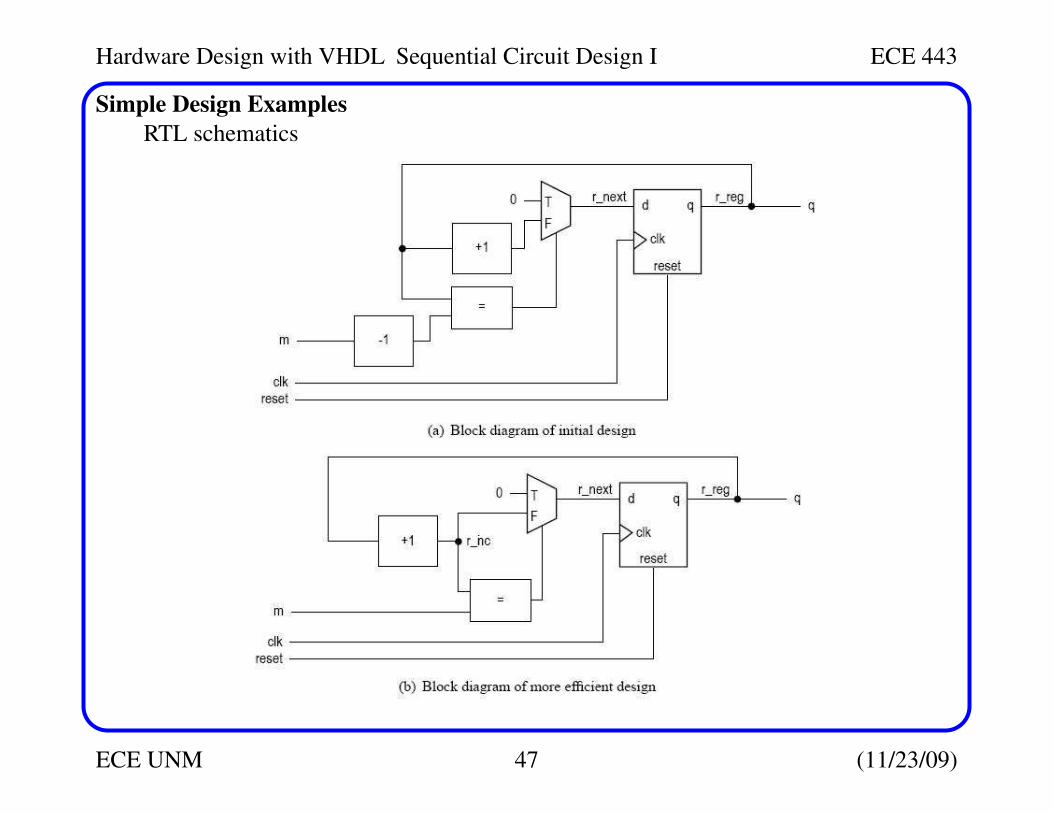
Hardware Design with VHDL Sequential Circuit Design I ECE 443
ECE UNM 47 (11/23/09)
Simple Design Examples
RTL schematics
Hardware Design with VHDL Sequential Circuit Design I ECE 443
ECE UNM 48 (11/23/09)
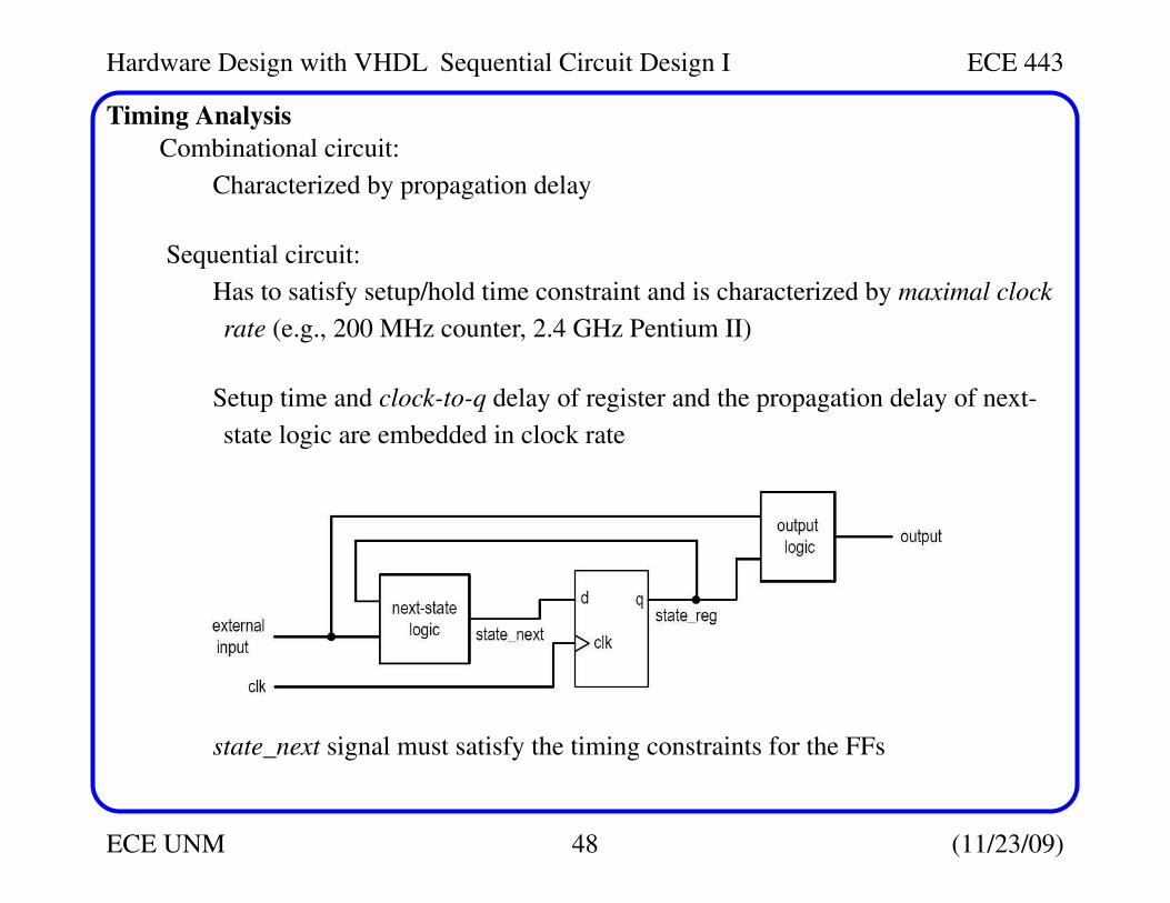
Timing Analysis
Combinational circuit:
Characterized by propagation delay
Sequential circuit:
Has to satisfy setup/hold time constraint and is characterized by maximal clock
rate (e.g., 200 MHz counter, 2.4 GHz Pentium II)
Setup time and clock-to-q delay of register and the propagation delay of next-
state logic are embedded in clock rate
state_next signal must satisfy the timing constraints for the FFs
Hardware Design with VHDL Sequential Circuit Design I ECE 443
ECE UNM 49 (11/23/09)
Timing Analysis
state_next delay is effected by three sources
• state_reg output -- part of the same loop and sync’ed by same clock (timing below)
• synchronized external input from a subsystem that uses the same clock
• unsynchronized external input -- must use synchronization circuit
For the first 2 items, we can adjust clock rate to prevent timing violations
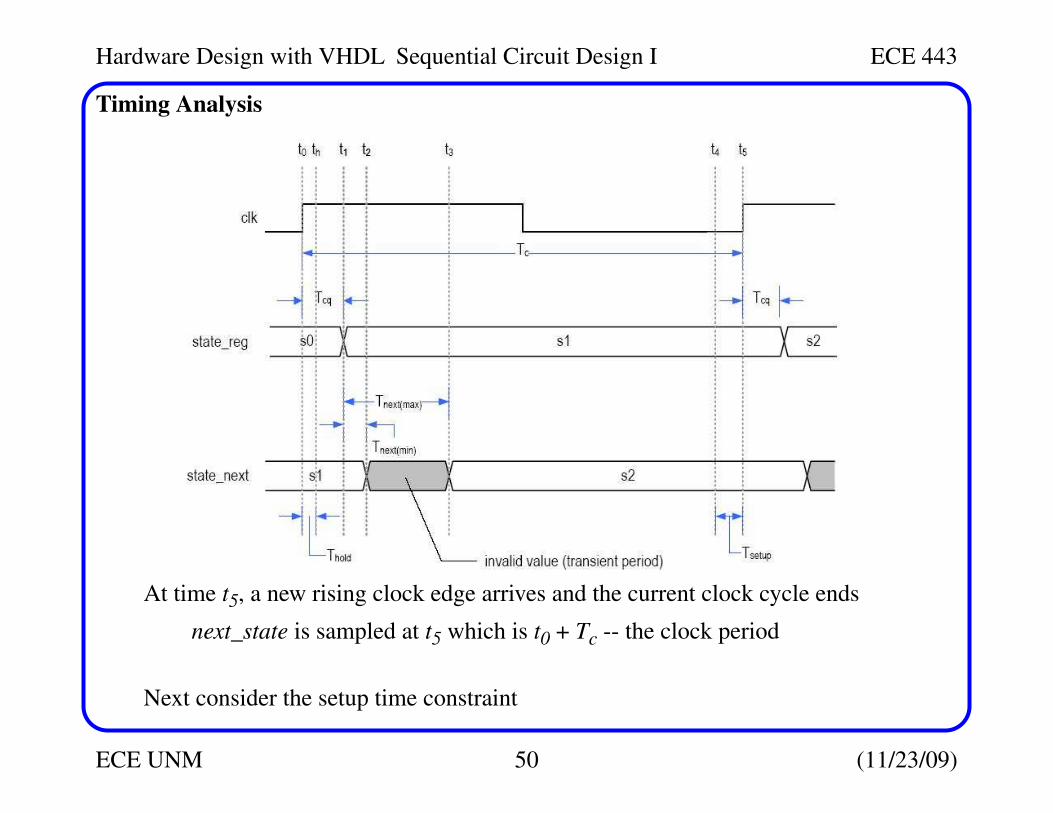
From the timing diagram below (which shows the timing behavior of the closed loop
system), at time t0, the clock changes from ’0’ to ’1’
We assume state_next does not change within the setup and hold periods
After the clock-to-q delay (Tcq), the register’s output, state_reg, stabilizes at time t1
(which is t0 + Tcq)
Since state_reg is input to the next-state logic, the output of next-state logic changes
at times Tnext(min) and Tnext(max) which represent fastest and slowest paths through it
Therefore, state_next changes at t2 (t1 + Tnext(min)) and stabilizes at t3 (t1 + Tnext(max))
Hardware Design with VHDL Sequential Circuit Design I ECE 443
ECE UNM 50 (11/23/09)
Timing Analysis
At time t5, a new rising clock edge arrives and the current clock cycle ends
next_state is sampled at t5 which is t0 + Tc -- the clock period
Next consider the setup time constraint
Hardware Design with VHDL Sequential Circuit Design I ECE 443
ECE UNM 51 (11/23/09)
Timing Analysis
The setup time constraint indicates that state_next MUST be stabilized at least Tsetup
before the next sampling edge at t5 -- given by t4 in the timing diagram
t3 < t4
From timing diagram
t3 = t0 + Tcq + Tnext(max)
t4 = t5 - Tsetup = t0 + Tc - Tsetup
The inequality above can be re-written as
t0 + Tcq + Tnext(max) < t0 + Tc - Tsetup
which simplifies to
Tcq + Tnext(max) + Tsetup < Tc
Therefore, minimal clock period is
Tc(min) = Tcq + Tnext(max) + Tsetup
Hardware Design with VHDL Sequential Circuit Design I ECE 443
ECE UNM 52 (11/23/09)
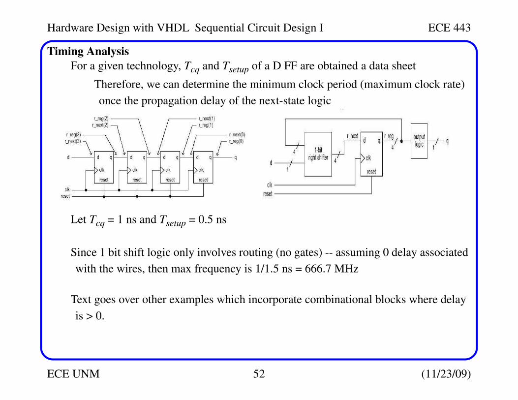
Timing Analysis
For a given technology, Tcq and Tsetup of a D FF are obtained a data sheet
Therefore, we can determine the minimum clock period (maximum clock rate)
once the propagation delay of the next-state logic
Let Tcq = 1 ns and Tsetup = 0.5 ns
Since 1 bit shift logic only involves routing (no gates) -- assuming 0 delay associated
with the wires, then max frequency is 1/1.5 ns = 666.7 MHz
Text goes over other examples which incorporate combinational blocks where delay
is > 0.
Hardware Design with VHDL Sequential Circuit Design I ECE 443
ECE UNM 53 (11/23/09)
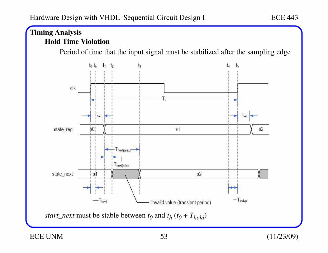
Timing Analysis
Hold Time Violation
Period of time that the input signal must be stabilized after the sampling edge
start_next must be stable between t0 and th (t0 + Thold)
Hardware Design with VHDL Sequential Circuit Design I ECE 443
ECE UNM 54 (11/23/09)
Timing Analysis
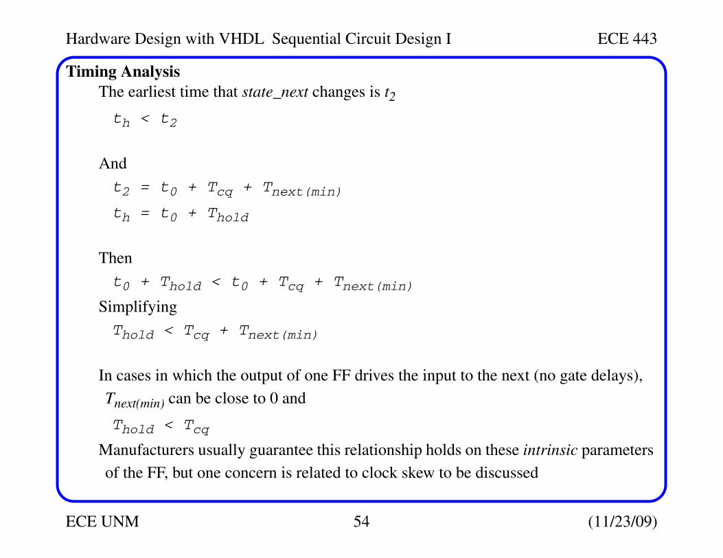
The earliest time that state_next changes is t2
th < t2
And
t2 = t0 + Tcq + Tnext(min)
th = t0 + Thold
Then
t0 + Thold < t0 + Tcq + Tnext(min)
Simplifying
Thold < Tcq + Tnext(min)
In cases in which the output of one FF drives the input to the next (no gate delays),
Tnext(min) can be close to 0 and
Thold < Tcq
Manufacturers usually guarantee this relationship holds on these intrinsic parameters
of the FF, but one concern is related to clock skew to be discussed
Hardware Design with VHDL Sequential Circuit Design I ECE 443
ECE UNM 55 (11/23/09)
Timing Analysis
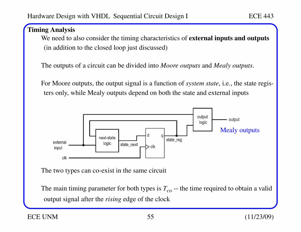
We need to also consider the timing characteristics of external inputs and outputs
(in addition to the closed loop just discussed)
The outputs of a circuit can be divided into Moore outputs and Mealy outputs.
For Moore outputs, the output signal is a function of system state, i.e., the state regis-
ters only, while Mealy outputs depend on both the state and external inputs
The two types can co-exist in the same circuit
The main timing parameter for both types is Tco -- the time required to obtain a valid
output signal after the rising edge of the clock
Mealy outputs
Hardware Design with VHDL Sequential Circuit Design I ECE 443
ECE UNM 56 (11/23/09)
Timing Analysis
Tco is the sum of the clock-to-q delay of the FF and propagation delay of the output
logic
Tco = Tcq + Toutput
Note that for Mealy, the input can affect the output directly
Text covers timing issues related to external synchronized inputs
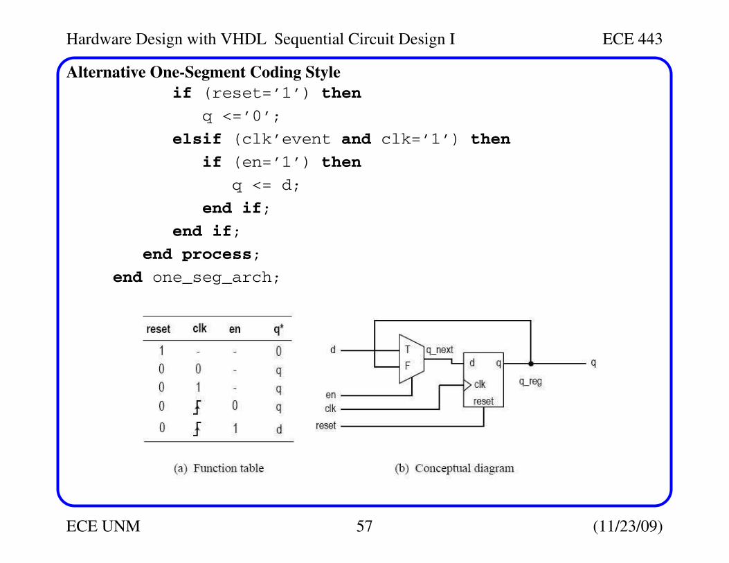
Alternative One-Segment Coding Style
Although it is possible to combine the memory elements with next-state and output
logic into one segment, you should avoid this coding practice b/c it is error prone
Consider the D FF with Sync Enable covered earlier
architecture one_seg_arch of dff_en is
begin
process(clk, reset)
begin
Hardware Design with VHDL Sequential Circuit Design I ECE 443
ECE UNM 57 (11/23/09)
Alternative One-Segment Coding Style
if (reset=’1’) then
q <=’0’;
elsif (clk’event and clk=’1’) then
if (en=’1’) then
q <= d;
end if;
end if;
end process;
end one_seg_arch;
Hardware Design with VHDL Sequential Circuit Design I ECE 443
ECE UNM 58 (11/23/09)
Alternative One-Segment Coding Style
The difference is the addition of the if (en = ’1’) then statement added inside the elsif
branch
We interpret this as "at the rising edge of clk, if en is ’1’, q gets the value of the d
input"
The absence of the else implies that if en is not ’1’, the q keeps its previous value
This correctly describes the function of the en signal
Consider the T FF discussed earlier
architecture one_seg_arch of tff is
signal q_reg: std_logic;
begin
process(clk, reset)
begin
if (reset=’1’) then
q_reg <= ’0’;
Hardware Design with VHDL Sequential Circuit Design I ECE 443
ECE UNM 59 (11/23/09)
Alternative One-Segment Coding Style
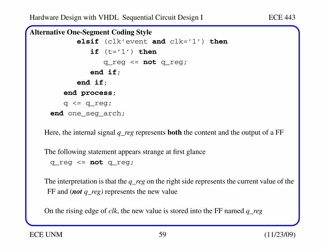
elsif (clk’event and clk=’1’) then
if (t=’1’) then
q_reg <= not q_reg;
end if;
end if;
end process;
q <= q_reg;
end one_seg_arch;
Here, the internal signal q_reg represents both the content and the output of a FF
The following statement appears strange at first glance
q_reg <= not q_reg;
The interpretation is that the q_reg on the right side represents the current value of the
FF and (not q_reg) represents the new value
On the rising edge of clk, the new value is stored into the FF named q_reg
Hardware Design with VHDL Sequential Circuit Design I ECE 443
ECE UNM 60 (11/23/09)
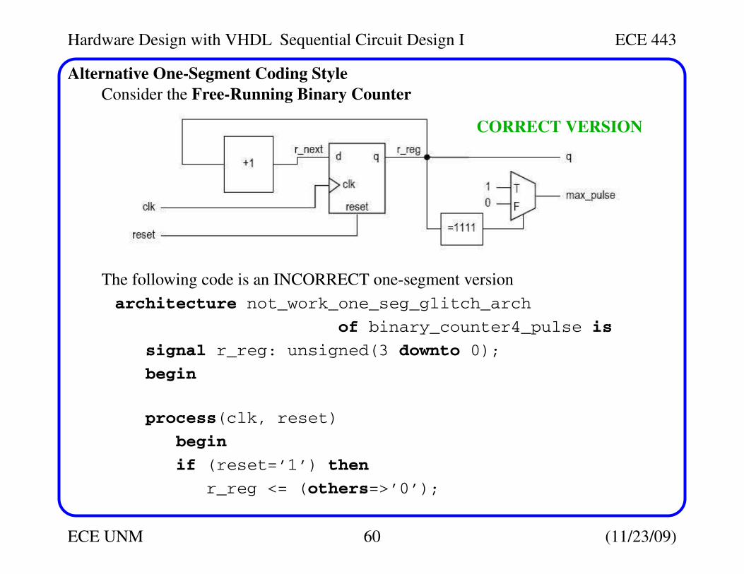
Alternative One-Segment Coding Style
Consider the Free-Running Binary Counter
The following code is an INCORRECT one-segment version
architecture not_work_one_seg_glitch_arch
of binary_counter4_pulse is
signal r_reg: unsigned(3 downto 0);
begin
process(clk, reset)
begin
if (reset=’1’) then
r_reg <= (others=>’0’);
CORRECT VERSION
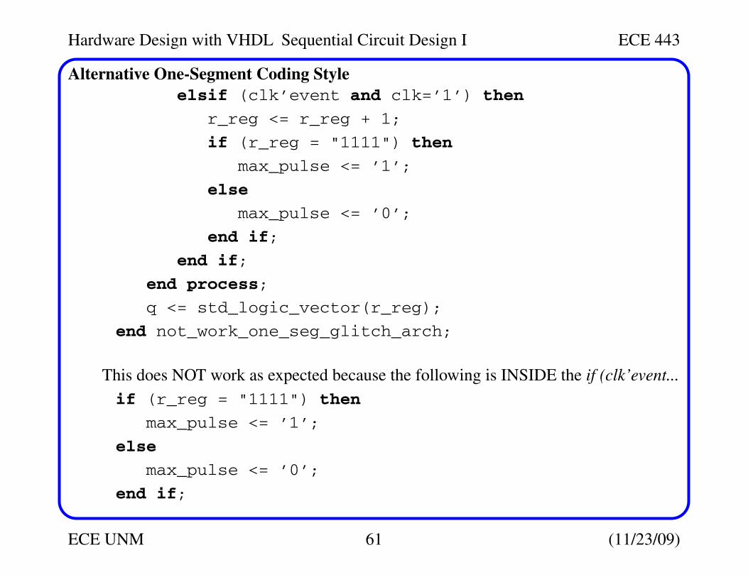
Hardware Design with VHDL Sequential Circuit Design I ECE 443
ECE UNM 61 (11/23/09)
Alternative One-Segment Coding Style
elsif (clk’event and clk=’1’) then
r_reg <= r_reg + 1;
if (r_reg = "1111") then
max_pulse <= ’1’;
else
max_pulse <= ’0’;
end if;
end if;
end process;
q <= std_logic_vector(r_reg);
end not_work_one_seg_glitch_arch;
This does NOT work as expected because the following is INSIDE the if (clk’event...
if (r_reg = "1111") then
max_pulse <= ’1’;
else
max_pulse <= ’0’;
end if;
Hardware Design with VHDL Sequential Circuit Design I ECE 443
ECE UNM 62 (11/23/09)
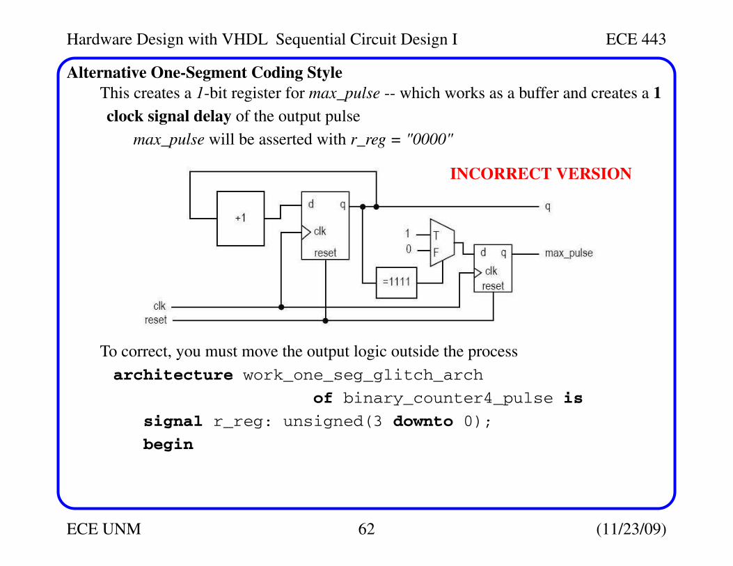
Alternative One-Segment Coding Style
This creates a 1-bit register for max_pulse -- which works as a buffer and creates a 1
clock signal delay of the output pulse
max_pulse will be asserted with r_reg = "0000"
To correct, you must move the output logic outside the process
architecture work_one_seg_glitch_arch
of binary_counter4_pulse is
signal r_reg: unsigned(3 downto 0);
begin
INCORRECT VERSION
Hardware Design with VHDL Sequential Circuit Design I ECE 443
ECE UNM 63 (11/23/09)
Alternative One-Segment Coding Style
process(clk, reset)
begin
if (reset=’1’) then
r_reg <= (others=>’0’);
elsif (clk’event and clk=’1’) then
r_reg <= r_reg + 1;
end if;
end process;
q <= std_logic_vector(r_reg);
max_pulse <= ’1’ when r_reg = "1111" else
’0’;
end work_one_seg_glitch_arch;
One more example -- consider the Programmable Counter
architecture not_work_one_arch of prog_counter is
signal r_reg: unsigned(3 downto 0);
begin
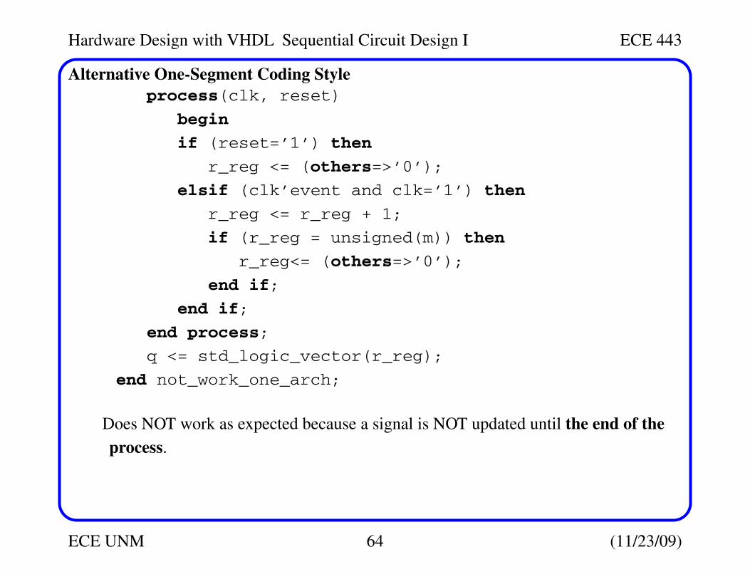
Hardware Design with VHDL Sequential Circuit Design I ECE 443
ECE UNM 64 (11/23/09)
Alternative One-Segment Coding Style
process(clk, reset)
begin
if (reset=’1’) then
r_reg <= (others=>’0’);
elsif (clk’event and clk=’1’) then
r_reg <= r_reg + 1;
if (r_reg = unsigned(m)) then
r_reg<= (others=>’0’);
end if;
end if;
end process;
q <= std_logic_vector(r_reg);
end not_work_one_arch;
Does NOT work as expected because a signal is NOT updated until the end of the
process.
Hardware Design with VHDL Sequential Circuit Design I ECE 443
ECE UNM 65 (11/23/09)
Alternative One-Segment Coding Style
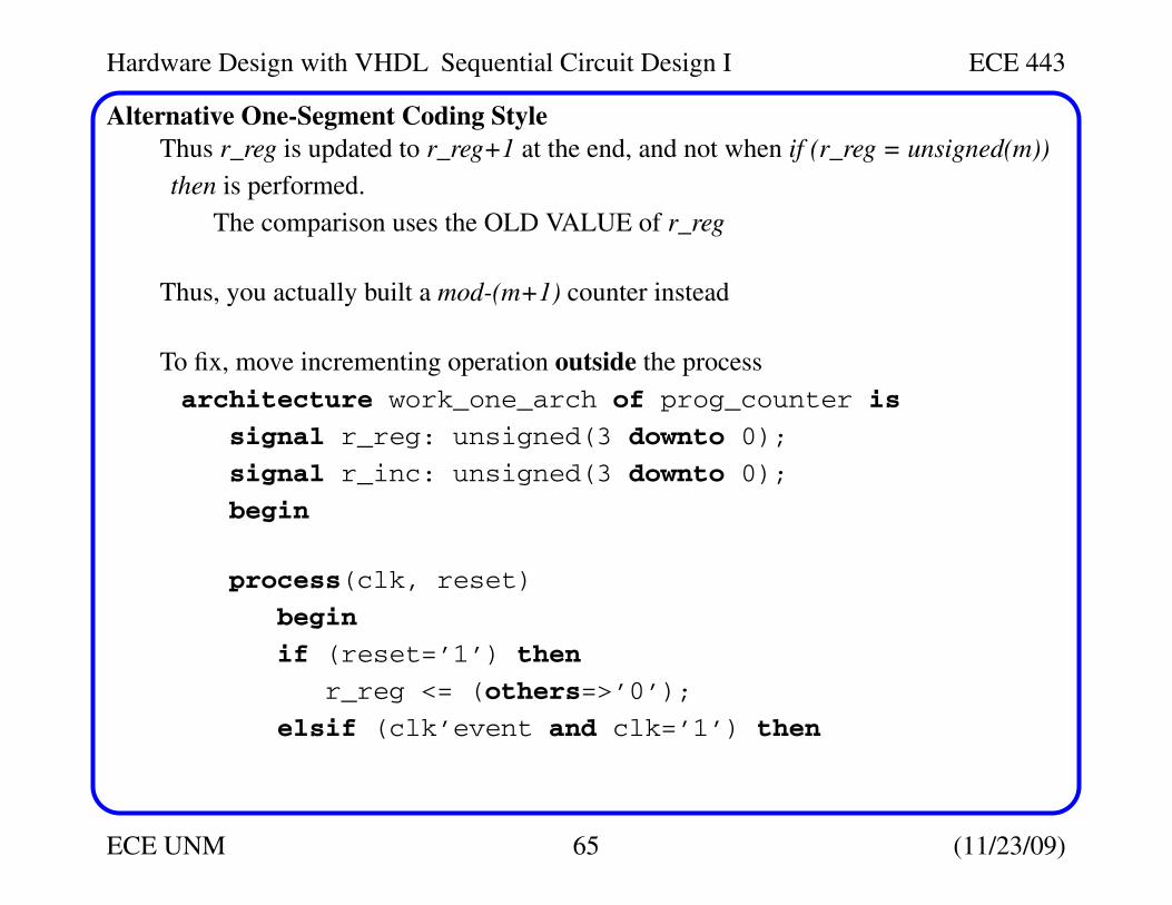
Thus r_reg is updated to r_reg+1 at the end, and not when if (r_reg = unsigned(m))
then is performed.
The comparison uses the OLD VALUE of r_reg
Thus, you actually built a mod-(m+1) counter instead
To fix, move incrementing operation outside the process
architecture work_one_arch of prog_counter is
signal r_reg: unsigned(3 downto 0);
signal r_inc: unsigned(3 downto 0);
begin
process(clk, reset)
begin
if (reset=’1’) then
r_reg <= (others=>’0’);
elsif (clk’event and clk=’1’) then
Hardware Design with VHDL Sequential Circuit Design I ECE 443
ECE UNM 66 (11/23/09)
Alternative One-Segment Coding Style
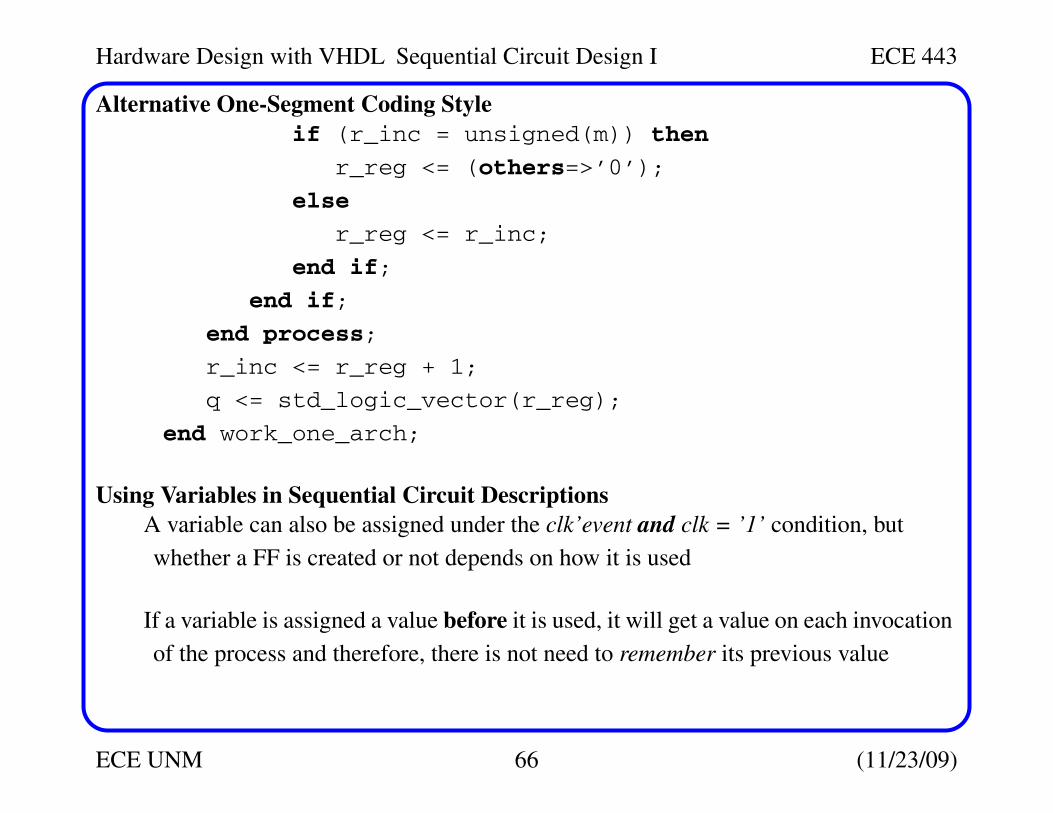
if (r_inc = unsigned(m)) then
r_reg <= (others=>’0’);
else
r_reg <= r_inc;
end if;
end if;
end process;
r_inc <= r_reg + 1;
q <= std_logic_vector(r_reg);
end work_one_arch;
Using Variables in Sequential Circuit Descriptions
A variable can also be assigned under the clk’event and clk = ’1’ condition, but
whether a FF is created or not depends on how it is used
If a variable is assigned a value before it is used, it will get a value on each invocation
of the process and therefore, there is not need to remember its previous value
Hardware Design with VHDL Sequential Circuit Design I ECE 443
ECE UNM 67 (11/23/09)
Using Variables in Sequential Circuit Descriptions
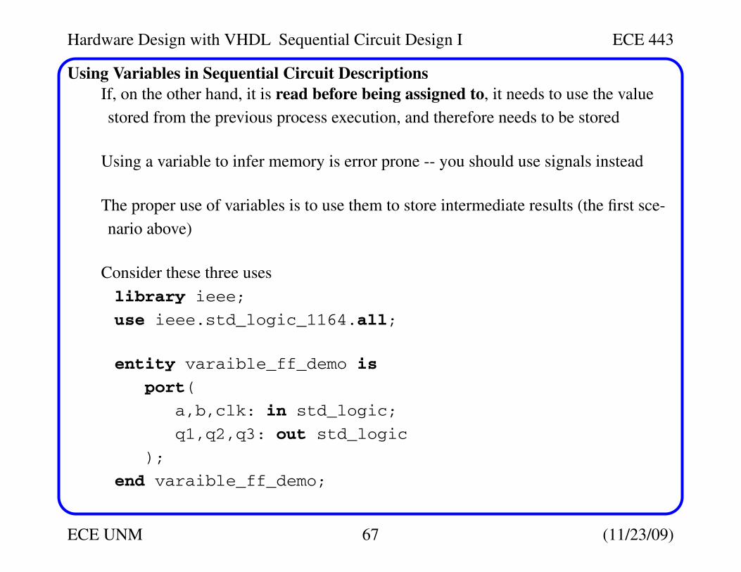
If, on the other hand, it is read before being assigned to, it needs to use the value
stored from the previous process execution, and therefore needs to be stored
Using a variable to infer memory is error prone -- you should use signals instead
The proper use of variables is to use them to store intermediate results (the first sce-
nario above)
Consider these three uses
library ieee;
use ieee.std_logic_1164.all;
entity varaible_ff_demo is
port(
a,b,clk: in std_logic;
q1,q2,q3: out std_logic
);
end varaible_ff_demo;
Hardware Design with VHDL Sequential Circuit Design I ECE 443
ECE UNM 68 (11/23/09)
Using Variables in Sequential Circuit Descriptions
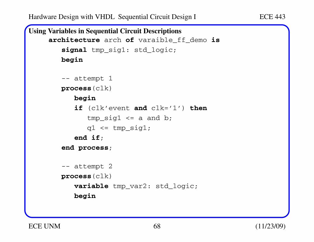
architecture arch of varaible_ff_demo is
signal tmp_sig1: std_logic;
begin
-- attempt 1
process(clk)
begin
if (clk’event and clk=’1’) then
tmp_sig1 <= a and b;
q1 <= tmp_sig1;
end if;
end process;
-- attempt 2
process(clk)
variable tmp_var2: std_logic;
begin
Hardware Design with VHDL Sequential Circuit Design I ECE 443
ECE UNM 69 (11/23/09)
Using Variables in Sequential Circuit Descriptions
if (clk’event and clk=’1’) then
tmp_var2 := a and b;
q2 <= tmp_var2;
end if;
end process;
-- attempt 3
process(clk)
variable tmp_var3: std_logic;
begin
if (clk’event and clk=’1’) then
q3 <= tmp_var3;
tmp_var3 := a and b;
end if;
end process;
end arch;
Hardware Design with VHDL Sequential Circuit Design I ECE 443
ECE UNM 70 (11/23/09)
Using Variables in Sequential Circuit Descriptions
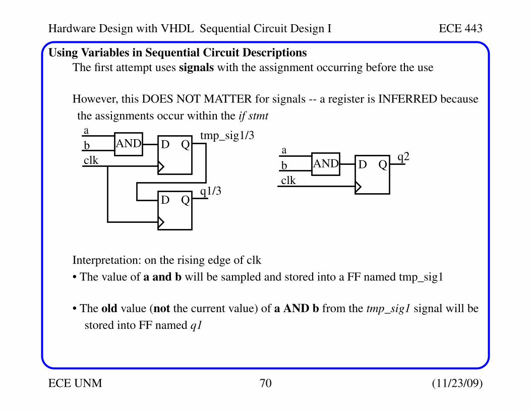
The first attempt uses signals with the assignment occurring before the use
However, this DOES NOT MATTER for signals -- a register is INFERRED because
the assignments occur within the if stmt
Interpretation: on the rising edge of clk
• The value of a and b will be sampled and stored into a FF named tmp_sig1
• The old value (not the current value) of a AND b from the tmp_sig1 signal will be
stored into FF named q1
D QANDa
b
D Q
clk
tmp_sig1/3
q1/3
D QANDb
clk
q2a
Hardware Design with VHDL Sequential Circuit Design I ECE 443
ECE UNM 71 (11/23/09)
Using Variables in Sequential Circuit Descriptions
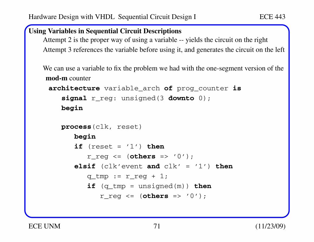
Attempt 2 is the proper way of using a variable -- yields the circuit on the right
Attempt 3 references the variable before using it, and generates the circuit on the left
We can use a variable to fix the problem we had with the one-segment version of the
mod-m counter
architecture variable_arch of prog_counter is
signal r_reg: unsigned(3 downto 0);
begin
process(clk, reset)
begin
if (reset = ’1’) then
r_reg <= (others => ’0’);
elsif (clk’event and clk’ = ’1’) then
q_tmp := r_reg + 1;
if (q_tmp = unsigned(m)) then
r_reg <= (others => ’0’);
Hardware Design with VHDL Sequential Circuit Design I ECE 443
ECE UNM 72 (11/23/09)
Using Variables in Sequential Circuit Descriptions
else
r_reg <= q_tmp;
end if;
end if;
end process;
q <= std_logic_vector(r_reg);
end variable_arch;
Recommended