Silver Nanowire Transparent Electrodes:
Fabrication, Characterization, and Device
Integration
by
Hadi Hosseinzadeh Khaligh
A thesis
presented to the University of Waterloo
in fulfillment of the
thesis requirement for the degree of
Master of Applied Science
in
Electrical and Computer Engineering -Nanotechnology
Waterloo, Ontario, Canada, 2013
©Hadi Hosseinzadeh Khaligh 2013

ii
AUTHOR'S DECLARATION
I hereby declare that I am the sole author of this thesis. This is a true copy of the thesis, including any
required final revisions, as accepted by my examiners.
I understand that my thesis may be made electronically available to the public.

iii
Abstract
Silver nanowire transparent electrodes have recently received much attention as a replacement
for indium tin oxide (ITO) for use in various electronic devices such as touch panels, organic
solar cells, and displays. The fabrication of silver nanowire electrodes on glass substrates with a
sheet resistance as low as 9 Ω/ and 90% optical transparency at 550 nm is demonstrated. These
resistance and transparency values match that of commercially available indium tin oxide and are
superior to other alternatives such as carbon nanotube electrodes. The nanowire electrodes are
low cost and easy to fabricate. Moreover, by depositing nanowire films on plastic substrates,
mechanically flexible electrodes are obtained. The silver nanowire electrodes are integrated into
several electronic devices: transparent heaters, organic solar cells, and switchable privacy glass.
The concerns about the suitability of silver nanowire electrodes for use in commercial electronic
devices are discussed. High surface roughness, one of the major concerns, is addressed by
introducing a new method of embedding silver nanowires in a soft polymer. The instability of
silver nanowire electrodes under current flow is also demonstrated for the first time. It is shown
that silver nanowire electrodes fail under current flow after as little as 2 days. This failure is
caused by Joule heating which causes the nanowires to break up and thus create an electrical
discontinuity in the nanowire film. Suggestions for improving the longevity of the electrodes are
given.

iv
Acknowledgements
I would like to thank Professor Irene Goldthorpe for all of her support, encouragement, and
guidance as my supervisor.
I am also thankful to my wife, for all her support, and patience.
Special thanks to my parents, who have been patient to my absence, what I have achieved in my
life belong to them.

v
Dedication
This thesis is dedicated to my parents and my wife who will be happy to see my graduation.

vi
Contents
List of Figures....................................................................................................................................viii
1 Introduction
1.1. Transparent electrodes .................................................................................................. 1
1.2. Carbon nanotube electrodes .......................................................................................... 5
1.3. Graphene electrodes ..................................................................................................... 7
1.4. Conductive polymers .................................................................................................... 9
1.5. Metal nanostructured electrodes ................................................................................... 9
1.5.1 Metal thin films and grids ............................................................................... 10
1.5.2 Metal nanowire electrodes .............................................................................. 11
1.5.3 Synthesis of silver nanowires ......................................................................... 13
1.5.4 Silver nanowire electrode challenges ............................................................. 14
1.6. Organization of this thesis .......................................................................................... 16
2 Fabrication and characterization of silver nanowire transparent electrodes
2.1 Introduction ................................................................................................................ 17
2.1.1 Solution deposition methods .......................................................................... 17
2.1.2 Transparency .................................................................................................. 18
2.1.3 Sheet resistance ............................................................................................... 20
2.2 Fabrication of silver nanowire transparent electrodes ................................................ 21
2.3 Characterization of silver nanowire transparent electrodes ........................................ 23
2.3.1 Transmittance and sheet resistance ................................................................. 23
2.3.2 Data comparison ............................................................................................. 25
2.3.3 Cost of silver nanowire films .......................................................................... 26
2.4 Flexibility of silver nanowire electrodes .................................................................... 27
2.5 Surface roughness ....................................................................................................... 28
2.6 Device integration ....................................................................................................... 31
3 Instability of silver nanowire transparent electrodes under current flow
3.1. Introduction ................................................................................................................ 33
3.2. Experiment.................................................................................................................. 34

vii
3.3. Results and discussion ................................................................................................ 35
3.3.1 Electrode failure measurements ...................................................................... 35
3.3.2 Failure mechanism characterization ............................................................... 37
3.3.3 Relevance to nanowire electrode design ........................................................ 41
3.4. Conclusions ................................................................................................................ 42
4 Silver nanowire transparent heaters
4.1 Introduction ................................................................................................................ 43
4.2 Experiment setup ........................................................................................................ 44
4.3 Results and discussion ................................................................................................ 45
4.4 Conclusions ................................................................................................................ 49
5 Conclusion and future work
5.1 Summary and conclusions .......................................................................................... 50
5.1 Future work................................................................................................................. 51
References ................................................................................................................................. 52

viii
List of Figures
Figure 1.1 (a) Structure of basic unit of an ITO/PEDOT-PSS/P3HT-PCBM/LiF/Al solar cell
[1]. (b) Structure of a resistive touch panel [2]. .............................................................................. 1
Figure 1.2 An ITO transparent heater being used as a defroster [3]. ............................................. 2
Figure 1.3 Optical spectra of typical ITO transparent conductors including both reflection (R)
and transmittance (T) [5]. ............................................................................................................... 3
Figure 1.4 Transmittance of ITO for different thicknesses (left). ITO film resistivity changes
depending on its thickness (right) [6]. ............................................................................................ 3
Figure 1.5 Single-wall carbon nanotube film [14] ......................................................................... 5
Figure 1.6 Sheet resistance versus transmittance for SWNT films with varying thicknesses,
before and after acid treatment [15]. Although the acid treatment reduces the resistance of the
films by reducing the junction resistances, the overall sheet resistance of the films is still much
higher than ITO. .............................................................................................................................. 6
Figure 1.7 Sheet resistance vs. transmittance for the highest conductivity CNT films. References
in plot [14-25]. ................................................................................................................................ 7

ix
Figure 1.8 A network of graphene flakes [25]. .............................................................................. 8
Figure 1.9 (a) Transmittance of a ca. 10 nm thick graphene flakes film (red), in comparison with
that of ITO (black) and FTO (blue) [27]. (b) Transmittance spectra for thin as-produced graphitic
films of various thicknesses [29]. ................................................................................................... 8
Figure 1.10 Average optical transmittance vs. electrical resistivity for Cr and Ni films compared
to unannealed and annealed ITO films [33]. ................................................................................. 10
Figure 1.11 SEM image of a silver grid transparent electrode, patterned by beam lithography
[34]. ............................................................................................................................................... 11
Figure 1.12 SEM images of Ag NW films with different densities. The different densities of Ag
NW films lead to different sheet resistances: (a) 100, (b), (c) 50, and (d) 15 Ω /. The diameters
of the Ag NWs are in the range of 40-100 nm [35]. ..................................................................... 12
Figure 1.13 Transmittance as a function sheet resistance for three alternatives [39]. ................. 13
Figure 1.14 Schematic illustration of silver nanowires grown in solution by the polyol method
[43]. ............................................................................................................................................... 14
Figure 1.15 (a) SEM image of a Ag NW network after mechanical pressing; AFM images of the
Ag NW network (b) before and (c) after pressing. The pressing significantly improves the

x
smoothness. The surface roughness decreases from 110 to 47 nm after mechanical pressing [31].
....................................................................................................................................................... 15
Figure 1.16 SEM image of electromigration effects due to current flow of 18-22 mA in single-
crystalline silver nanowires [46]. .................................................................................................. 16
Figure 2.1 Various solution deposition methods [48] .................................................................. 18
Figure 2.2 Structure of a Mayer rod [49] ..................................................................................... 18
Figure 2.3 Schematic set-up of spectrophotometer for measuring specular transmittance ......... 19
Figure 2.4 Schematic set up of using an integrated sphere to measure diffusive transmittance
[50] ................................................................................................................................................ 20
Figure 2.5 Two resistors with the same sheet resistance and total resistance [51] ...................... 21
Figure 2.6 Silver nanowires solution with concentration of 5 mg/ml .......................................... 22
Figure 2.7 (a) Schematic illustration of the Mayer rod coating method [52], (b) Mayer rod and
glass substrates for fabrication of transparent electrode ............................................................... 22
Figure 2.8 (a) Fabricated silver nanowire transparent electrode (b) SEM image of silver
nanowire film on glass substrate ................................................................................................... 23

xi
Figure 2.9 (a) Transparency vs. wavelength of two silver nanowire transparent electrodes
including the glass substrates (transmittance of the plain glass is 91% at 550nm) (b)
Transparency of the electrodes excluding the glass substrate (glass is used as a reference) ........ 25
Figure 2.10 Transparency versus sheet resistance for several transparent electrode materials. The
data for the silver nanowire electrodes are from my own experimetns and references for the
remainder of the data in the plot is from [53–57]. ........................................................................ 26
Figure 2.11 Resistance changes of flexible silver nanowire transparent electrode under a 140ᵒ
bending angle. ............................................................................................................................... 28
Figure 2.12 (a) AFM image of as-deposited film of silver nanowire (b) The height of the surface
along a linear scan ......................................................................................................................... 28
Figure 2.13 SEM image of a silver nanowire electrode (a) after deposition (b) after pressing. .. 29
Figure 2.14 schematic of silver nanowire embedding process .................................................... 30
Figure 2.15 AFM image of pressed film of silver nanowire (left), and embedded silver
nanowires on a soft polymer (right) .............................................................................................. 31
Figure 2.16 Photovoltaic device structure used for the fabrication of inverted devices. ............. 31

xii
Figure 2.17 Illumination curves through the ITO side and the silver nanowire side of the
inverted solar cells prepared using silver nanowires and P3HT/PCBM ....................................... 32
Figure3.1 (a) SEM image of an as-prepared electrode. (b) Voltage and surface temperature of a
12 Ω/ sample when a constant current density of 17 mA/cm2 was applied across the electrode.
....................................................................................................................................................... 35
Figure 3.2 (a) The number of days to failure versus sheet resistance, when conducting 17
mA/cm2 across samples with different resistances. (b) The relationship between the number of
days to failure and current density, as measured with three different 30 Ω/ electrode .............. 36
Figure 3.3 SEM images of a silver nanowire electrode after a constant current density of 17
mA/cm2 was passed across it (a,b) for 17 days with a sheet resistance of 12 Ω/, and (b,c) for 17
hour with a sheet resistance of 36 Ω/ ......................................................................................... 37
Figure 3.4 SEM images of silver nanowire electrodes annealed on a glass substrate for (a) 7
days, (b) 14 days, and (c) 17 days at 100 °C, (d) 17 days at 150 °C. ........................................... 39
Figure 3.5 silver nanowires annealed at 300 (a) for half an hour (b) for one and half hour. ....... 39
Figure 3.6 Energy dispersive spectrum of a nanoparticle formed on a silver nanowire after
electrode failure. The x indicates the location where the measurement was taken. Sulfur was
detected in the nanoparticles indicating corrosion of the silver. ................................................... 41

xiii
Figure 4.1 Schematic setup of experiment for measuring the transparent heater performance ... 45
Figure 4.2 Heating profile of the transparent heaters with 92% transmittance at 550 nm (a) on
PET with sheet resistance of 22 Ω/ (b) on glass with sheet resistance of 15 Ω/. The labelled
voltages are the voltage applied across the films and the power density is stated in brackets. .... 46
Figure 4.3 Maxiumum surface temperature vs. power density for nanowire heaters with various
sheet resistances on (a) PET and (b) glass. ................................................................................... 48
Figure 4.4 Heating profiles of the transparent heaters on the glass substrates with various
transmittances under applied voltage of 6 V................................................................................. 48
Figure 4.5 Temperature and resistance changes of a silver nanowire heater with a sheet
resistance of 24 Ω/ during 4 days of appling 4.5 V across its terminals .................................... 49

1
Chapter 1
Introduction
1.1. Transparent electrodes
Transparent electrodes are a crucial part of many electronic devices such as organic solar cells,
displays (e.g. Liquid Crystal Displays (LCDs)), touch panels, and transparent heaters.
Transparent electrode thin films are optically transparent to visible light and also electrically
conductive, and are used in applications where light needs to enter or leave a device. For
instance, in organic solar cells a transparent electrode acts as either an anode or cathode and
completes the solar cell circuit while at the same time lets visible light pass through the film to
generate charge carriers [1]. Figure 1.1a shows a schematic of an organic solar cell. In this
structure, indium tin oxide (ITO), which is a transparent conductive film deposited on a glass
substrate, is used as the anode of the device.
Figure 1.1 (a) Structure of basic unit of an organic solar cell [1]. (b) Structure of a resistive touch panel [2].
(a) (b)

2
Transparent electrodes are also used in touch panels, as illustrated in Figure 1.1b [2]. This device
consists of two layers of transparent electrodes. Also on the market are transparent heaters, made
of transparent electrodes and used to remove frost from displays, cameras and also ski goggles in
cold environments. Figure 1.2 shows a commercial example of an ITO transparent heater [3].
Figure 1.2 An ITO transparent heater being used as a defroster [3].
The most common materials used for transparent electrodes are metal oxides, particularly ITO
which is the most popular material for transparent electrodes. ITO can provide highly transparent
electrodes (80-95%) with low sheet resistances (10-1000 Ω/).
Metal oxides are transparent because their band gap energies are larger than the energies of
photons in the visible range. The band gap of ITO, for example, is 3.8 eV [4]. Figure 1.3 shows
the optical spectra of ITO, which is typical for metal oxide transparent electrodes. The sample
with a sheet resistance of 10.98 Ω/ in the figure is about 80% transparent at wavelengths
between 400 and 700 nm; in this region, film interference effects can be seen in both the
transmission and reflection spectra. High absorption below 300 nm wavelengths is due to the
band gap of the material. Above 1000 nm, transmittance decreases drastically which corresponds
to collective oscillations of conduction band electrons, known as plasma oscillations or plasmons
[4].

3
Figure 1.3 Optical spectra of typical ITO transparent conductors including both reflection (R) and transmittance (T)
[5].
For a particular application, the transparency and sheet resistance of an ITO film can be
controlled through the film thickness [4]. Figure 1.4 shows that there is a trade-off between
transparency and resistance; lower resistivity films require a thicker ITO layer, which results in
lower transparency.
Figure 1.4 Transmittance of ITO for different thicknesses (left). ITO film resistivity changes depending on its
thickness (right) [6].

4
In the last decade, the number of electronic displays and touch screens has increased drastically.
For example, 362 million touch panels were produced in 2010 with an increase of 20% each year
up to 2013 [7]. In addition, new device technologies call for new features for transparent
electrodes like flexibility, easy fabrication processes, low cost and light weight.
ITO cannot meet all the new expected qualifications for the innovative next generation of
electronics. ITO has ceramic properties, so it is not flexible; a small amount of strain as low as 2-
3% can initiate cracks in ITO film on flexible substrates, which reduces electrode conductivity
and thus performance of the device dramatically [8]. Secondly, indium is a rare material and the
price of indium is volatile with an overall increasing trend [9]. Thirdly, the fabrication of ITO is
costly since it requires high temperatures and a high vacuum for control over the thickness and
doping concentration [9] Also, it is deposited by sputtering which can damage underlying layers
in the case of organic devices. Fourthly, ITO also has a high index of refraction, which is not
suitable for display applications since it reflects light whereby decreasing the brightness of the
screen. An additional coating needs to be applied to solve this problem, leading to additional
cost.
Extensive research has been devoted to solving problems associated with ITO transparent
electrodes. For example, to make a flexible ITO transparent electrode, ITO has been laminated
onto flexible substrates like polyethylene terephthalate (PET), and ITO elements in various ratios
have been investigated to improve the mechanical properties of the film [9]. However, these
approaches not only add additional manufacturing cost but also reduce the optical and electrical
performance of such electrodes so they cannot compete in the current growing market.
Therefore, over the past decade many researchers have tried to find an alternative material to
replace ITO. So far they have made significant advances in introducing new potential candidates

5
for transparent electrodes. However, each candidate has advantages and disadvantages and more
investigation is need before any of them can be used commercially. Current significant materials
for substitution are carbon nanotubes (CNTs), graphene, transparent conductive polymers, metal
grids, and random meshes of metal nanowires.
1.2. Carbon nanotube electrodes
The first CNTs were synthesized in 1990 [10]. A single carbon nanotube can have electron
mobilities higher than 100 000 cm2/V.s [11] and CNTs have also been shown to have unique and
beneficial optical and mechanical properties [12-13]. Films of CNTs appeared in the mid-2000s
as a new material for transparent electrodes as illustrated in Figure 1.5 [9]. Although it was
thought they would be a suitable ITO substitute because of their high mobility, challenges
emerged for CNT films.
Figure 1.5 Single-wall carbon nanotube film [14]
The most important challenge relates to the conductivity of CNT films, which is limited by the
junction resistance where nanotubes overlap. These junctions between nanotubes have high
resistance in the range of 200 kΩ - 20 MΩ [11]; hence, the conductivity of CNT films is reduced
drastically compared to that of a single CNT. Some approaches have been introduced to reduce
the sheet resistance of the CNT films such as treating CNTs with acid and using longer CNTs

6
[9]. Figure 1.6 shows the sheet resistance vs. transmittance of a CNT film before and after acid
treatment [15]. However, films of CNTs still have much lower conductivity than conventional
ITO films. A related problem to the junction resistance is that CNTs can be either metallic or
semiconducting. In CNT fabrication, semiconductor and metal CNT are fabricated at the same
time so the CNT films consist of both types. The semiconductor nanotubes have much lower
conductivity than the metallic tubes [11] and so do not contribute much to the conductivity.
However, the semiconductor nanotubes absorb light and so reduce transparency. In addition,
metal/semiconductor junctions in CNT films create high contact resistance due to Schottky
barrier formation, resulting in higher sheet resistance [11]. Separating metal and semiconductor
CNTs or producing metallic only CNT are still serious challenges. Although some methods have
been introduced to separate metal nanotubes, they are expensive and not suitable for commercial
use [6].
Figure 1.6 Sheet resistance versus transmittance for single-wall nanotubes (SWNT) films with varying thicknesses,
before and after acid treatment [15]. Although the acid treatment reduces the resistance of the films by reducing the
junction resistances, the overall sheet resistance of the films is still much higher than ITO.
The best results for CNT transparent electrodes are gathered in Figure 1.7 [16], and show a
significant progress in fabricating transparent electrodes based on CNTs during recent years.
However, most applications require lower sheet resistances and higher transparency than even

7
the best values shown in the plot and thus CNT films at this time are not a suitable replacement
for ITO [17–25].
Figure 1.7 Sheet resistance vs. transmittance for the highest conductivity CNT films. References in plot [14-25].
1.3. Graphene electrodes
Graphene is a thin layer of carbon atoms bonded with sp2 orbitals. Among the interesting
properties of graphene is the capability of adding external dopants which results in high in-plane
conductivity of graphene sheets. The thickness of the graphene sheets is in the order of a few
nanometers and thus, the graphene sheets are relatively transparent to visible light.
The major concern regarding graphene is that fabrication of a single sheet of graphene on a large
scale is difficult. More often, instead of a single sheet of graphene, networks of graphene flakes
are synthesized. These flakes result in very high sheet resistance, in the range of several kΩ [9],
because there is a high contact resistance between flakes so the overall conductivity is low [26-
27]. Figure 1.8 shows the boundaries and contact areas that cause high resistivity.

8
Figure 1.8 A network of graphene flakes [25].
Figure 1.9a compares ITO and fluorine tin oxide (FTO), both widely used in electronics, with a
graphene flakes film of 10 nm thickness [28]. Although the conductivity of graphene sheets can
be in an acceptable range, the transparency of graphene is significantly lower than that of the
current commercial materials. It has been shown in Figure 1.9b that the transparency of graphene
films depends on the thickness of the graphene layer. As typical for transparent electrodes of any
material, thinner graphene film results in higher transparency but higher sheet resistance [29].
Figure 1.9 (a) Transmittance of a ca. 10 nm thick graphene flakes film (red), in comparison with that of ITO (black)
and FTO (blue) [27]. (b) Transmittance spectra for thin as-produced graphitic films of various thicknesses [29].
Extensive improvements have been made in fabrication processes for graphene films and in
integrating them into electronic devices. Although researchers have introduced new methods of
fabricating a single sheet of graphene, such as the high temperature CVD method, the cost of this
(Graphene)
(ITO)
(FTO)

9
method is relatively high [29] and the sheet resistances in these single sheets are still not low
enough to be useful in most applications.
1.4. Conductive polymers
Transparent conductive polymers appeared in the mid 20th
century and attracted researchers’
attention because of their interesting properties like high flexibility, low cost and light weight.
Several companies have been trying to use them in various devices such as touch panels and
organic electronics [30]. The combination of Poly (3, 4-ethylenedioxythiophene) and poly
(styrene sulfonate), known as PEDOT:PSS, is one of the most common materials on the market
being used in organic electronics.
One of the major problems of conducting polymers is their instability in air due to absorption of
oxygen and moisture. For example, PEDOT:PSS degrades in air in a short time. To solve this
problem, extensive research is being done to synthesize more stable conducting polymers.
Recently, Fujitsu company has used a type of polythiophene, which is more stable in air, for their
organic touch panels [30]. In addition to stability, another major problem is that the conductivity
of transparent conductive polymers is low and can therefore not replace ITO in many
applications. One possibility is to combine conducting polymers with other materials such as
graphene and nanostructured metals to enhance the conductivity [31,32].
1.5. Metal nanostructured electrodes
Because of the low conductivity of CNT films, graphene, and transparent conducting polymers,
metal nanostructures are an appealing alternative. Metals have the highest conductivity of all
types of materials. However, because of the very low transparency of metals to visible light,
fabrication of transparent metallic electrodes was not easy until recent decades. Since the
emergence of nanotechnology and nanostructured materials, fabricating transparent electrodes
10
using metallic structures has become easier. Metal nano-grids, thin metal films (of less than 10
nm thickness) and random meshes of metal nanowires are three common structures used to make
transparent electrodes [9].
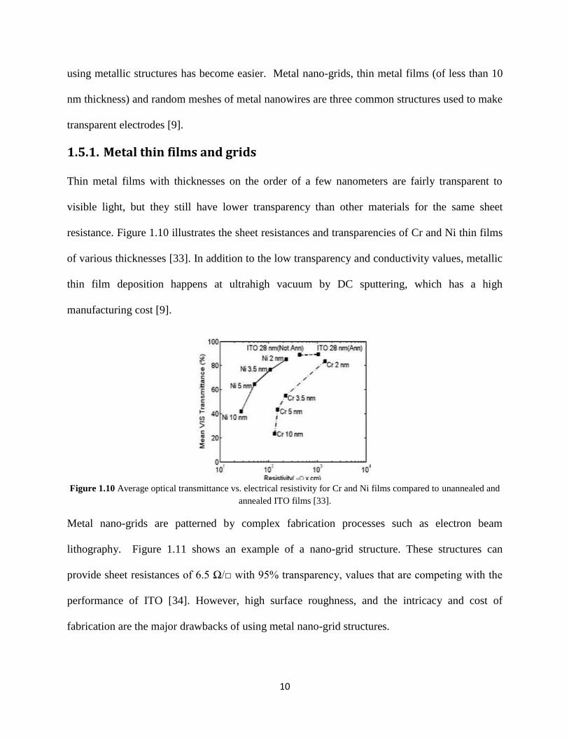
1.5.1. Metal thin films and grids
Thin metal films with thicknesses on the order of a few nanometers are fairly transparent to
visible light, but they still have lower transparency than other materials for the same sheet
resistance. Figure 1.10 illustrates the sheet resistances and transparencies of Cr and Ni thin films
of various thicknesses [33]. In addition to the low transparency and conductivity values, metallic
thin film deposition happens at ultrahigh vacuum by DC sputtering, which has a high
manufacturing cost [9].
Figure 1.10 Average optical transmittance vs. electrical resistivity for Cr and Ni films compared to unannealed and
annealed ITO films [33].
Metal nano-grids are patterned by complex fabrication processes such as electron beam
lithography. Figure 1.11 shows an example of a nano-grid structure. These structures can
provide sheet resistances of 6.5 Ω/ with 95% transparency, values that are competing with the
performance of ITO [34]. However, high surface roughness, and the intricacy and cost of
fabrication are the major drawbacks of using metal nano-grid structures.

11
Figure 1.11 Scanning electron microscopy (SEM) image of a silver grid transparent electrode, patterned by beam
lithography [34].
1.5.2. Metal nanowire electrodes
Metal nanowires are considered to be a 1D nanostructure; they have the shape of a wire, where
the diameter is typically less than 100 nm, and their length is 1 µm or more. Metal nanowires
such as copper or silver can be synthesized in solution, and then deposited on transparent
substrates such as glass or plastic to create a random conductive mesh. These films are similar to
CNT films, except in this case all wires are metallic. The mesh transparency can reach 90% for a
sheet resistance below 10Ω/, which makes the transparency and conductivity similar to that of
ITO and thus suitable for transparent electrode applications [35]. Figure 1.12 show a random
network of transparent electrode based on silver nanowires with various densities of nanowires.
Sheet resistance and transparency of the films can be controlled by varying the density of the
deposited solution to get specific properties [35]. As is the case for most transparent electrodes,
there is a trade-off between transparency and conductivity: denser films of nanowires are more
conductive but less transparent.

12
Figure 1.12 SEM images of Ag NW films with different densities. The different densities of Ag NW films lead to
different sheet resistances: (a) 100, (b), (c) 50, and (d) 15 Ω /. The diameters of the Ag NWs are in the range of 40-
100 nm [35].
Simple and cheap fabrication, high transparency, and low sheet resistance are advantages of
metal nanowire structures. And although silver is an expensive element, so little of it is used in a
nanowire film that material costs are lower than ITO. Moreover, the nanowire electrodes are
mechanically flexible. They are also much more transparent in the infrared (IR) range than ITO
which makes them more suitable for multi-junction solar cells and other applications where
transparency in the IR is required. A solution of silver nanowires can be deposited in atmosphere
using simple and inexpensive deposition methods like spin coating [36], spray coating [37], and
Meyer rod coating [35]. Silver is one of the most promising nanowire electrode materials since
silver has the highest conductivity amongst metals. Moreover, silver nanowire films can be
fabricated either at room temperature [38], or at low annealing temperatures [35], which make
them compatible with plastic substrates in producing flexible electrodes.
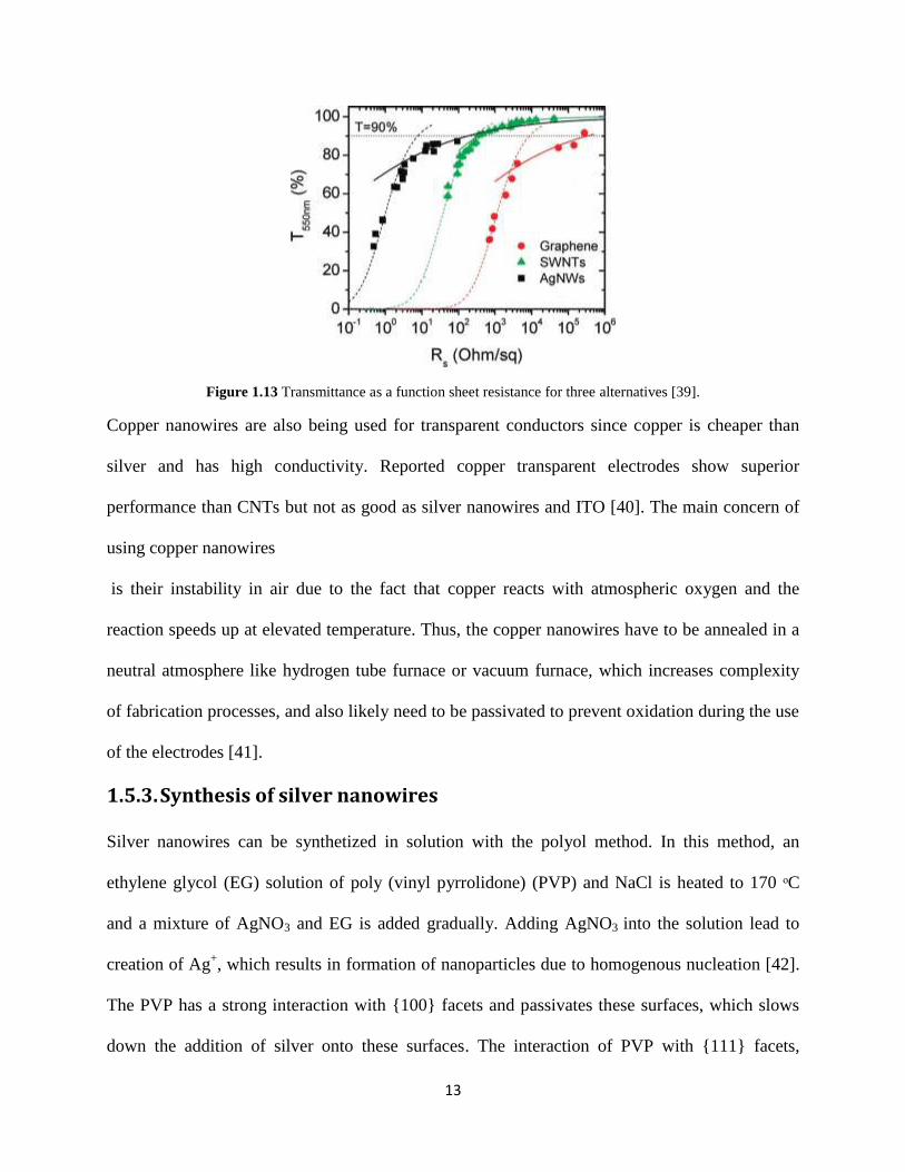
Figure 1.13 compares silver nanowire electrodes with other alternatives. So far, silver nanowire
electrodes show superior performance compared to graphene and CNTs.
13
Figure 1.13 Transmittance as a function sheet resistance for three alternatives [39].
Copper nanowires are also being used for transparent conductors since copper is cheaper than
silver and has high conductivity. Reported copper transparent electrodes show superior
performance than CNTs but not as good as silver nanowires and ITO [40]. The main concern of
using copper nanowires
is their instability in air due to the fact that copper reacts with atmospheric oxygen and the
reaction speeds up at elevated temperature. Thus, the copper nanowires have to be annealed in a
neutral atmosphere like hydrogen tube furnace or vacuum furnace, which increases complexity
of fabrication processes, and also likely need to be passivated to prevent oxidation during the use
of the electrodes [41].
1.5.3. Synthesis of silver nanowires
Silver nanowires can be synthetized in solution with the polyol method. In this method, an
ethylene glycol (EG) solution of poly (vinyl pyrrolidone) (PVP) and NaCl is heated to 170 ᵒC
and a mixture of AgNO3 and EG is added gradually. Adding AgNO3 into the solution lead to
creation of Ag+, which results in formation of nanoparticles due to homogenous nucleation [42].
The PVP has a strong interaction with 100 facets and passivates these surfaces, which slows
down the addition of silver onto these surfaces. The interaction of PVP with 111 facets,
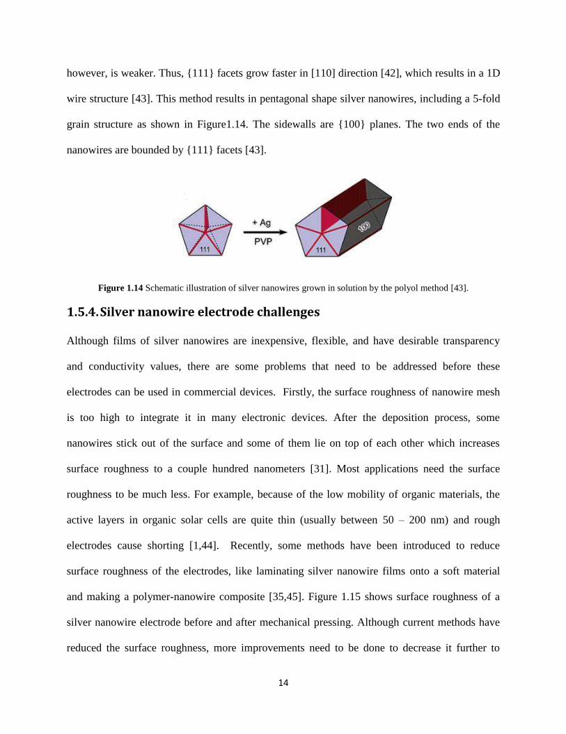
14
however, is weaker. Thus, 111 facets grow faster in [110] direction [42], which results in a 1D
wire structure [43]. This method results in pentagonal shape silver nanowires, including a 5-fold
grain structure as shown in Figure1.14. The sidewalls are 100 planes. The two ends of the
nanowires are bounded by 111 facets [43].
Figure 1.14 Schematic illustration of silver nanowires grown in solution by the polyol method [43].
1.5.4. Silver nanowire electrode challenges
Although films of silver nanowires are inexpensive, flexible, and have desirable transparency
and conductivity values, there are some problems that need to be addressed before these
electrodes can be used in commercial devices. Firstly, the surface roughness of nanowire mesh
is too high to integrate it in many electronic devices. After the deposition process, some
nanowires stick out of the surface and some of them lie on top of each other which increases
surface roughness to a couple hundred nanometers [31]. Most applications need the surface
roughness to be much less. For example, because of the low mobility of organic materials, the
active layers in organic solar cells are quite thin (usually between 50 – 200 nm) and rough
electrodes cause shorting [1,44]. Recently, some methods have been introduced to reduce
surface roughness of the electrodes, like laminating silver nanowire films onto a soft material
and making a polymer-nanowire composite [35,45]. Figure 1.15 shows surface roughness of a
silver nanowire electrode before and after mechanical pressing. Although current methods have
reduced the surface roughness, more improvements need to be done to decrease it further to

15
make those electrodes practical for organic solar cells and displays. The issue of surface
roughness will be addressed in my own work in subsection 2.5.
Figure 1.15 (a) SEM image of a Ag NW network after mechanical pressing; AFM images of the Ag NW network
(b) before and (c) after pressing. The pressing significantly improves the smoothness. The surface roughness
decreases from 110 to 47 nm after mechanical pressing [31].
A second problem, which has not received much attention up to this point, is the stability of
silver nanowires over long periods of time. For example, silver is known to be susceptible to
electromigration, where the flow of current causes the gradual movements of ions in a conductor.
As illustrated in Figure 1.16, the flow of current through a silver nanowire can result in a void
and hillock structure on two ends. This particular study was carried out on single crystalline
nanowires [46], but the effects of this phenomenon have not been investigated for nanowires
synthesized by the polyol process, which have grain boundaries, and not for meshes of
nanowires. In addition to electromigration, it is also known that nanowires are unstable at
temperatures as low as 200 °C or perhaps even less [47]. In Chapter 3, I will report on the
results of experiments to access the stability of nanowire electrodes, report characterization
results which help determine the cause of the instability, and provide suggestions for improving
the stability of silver nanowire transparent electrodes.

16
Figure 1.16 SEM image of electromigration effects due to current flow of 18-22 mA in single-crystalline silver
nanowires [46].
1.6. Organization of this thesis
A method of silver nanowire transparent electrodes fabrication is reported in Chapter 2 and the
electrode characteristics are discussed and compared with those of other reports. Results of a
new method to reduce the surface roughness are also illustrated in Chapter 2.
This thesis also contributes to this area by investigating the instability of silver nanowire
electrodes under current flow and investigates failure mechanisms (Chapter 3). Suggestions for
how these electrodes can be better designed for improved longevity are given. In Chapter 4, a
new application of silver nanowire, transparent heaters, is introduced. Lastly, I summarize my
work in Chapter 5 and give suggestions for future work.

17
Chapter 2
Fabrication and characterization of silver nanowire
transparent electrodes
This chapter describes a method for fabricating silver nanowire transparent electrodes and shows
their optical and electrical characteristics. The performance of the fabricated electrodes is
compared to that of the other reports. Silver nanowire films flexibility is also discussed and a
new method of roughness reduction is introduced.
2.1 Introduction
2.1.1 Solution deposition methods
Solution synthesized silver nanowires are dispersed in an alcoholic solvent such as isopropyl
alcohol (IPA), ethanol or methanol and can be deposited on various substrates using solution
deposition methods. Figure 2.1 illustrates the various solution deposition methods that exist to
deposit solutions into thin films or patterns. Spin coating is the most popular method for lab-
scale samples due to its simplicity and reproducibility. However, for large-scale fabrication,
other methods like spray coating, doctor blade coating, or wire-wound metering rod (Mayer rod)
coating are more suitable and used more frequently in industry. Since transparent electrodes need
to be fabricated in large-scale eventually, I chose the Mayer rod coating method, which is
compatible with roll-to-roll techniques and more convenient for industry. This method is
inexpensive and easy to use, just one wire-wound rod is enough for fabrication, so there is no
need for any complex equipment. Moreover, using this method, the solution is distributed
uniformly on the substrate

18
Figure 2.1 Various solution deposition methods [48]
Figure 2.2 shows the schematic of a Mayer rod. The diameter of the wound wire determines
the thickness of the deposited solution.
a)
Figure 2.2 Structure of a Mayer rod [49]
2.1.2 Transparency
When light encounters an object, the incident light can be transmitted, absorbed or reflected by
the object. The ratio of transmitted light to the incident light is defined as transmittance of the
object, which is usually shown in percentages. Transmittance of an object can vary in response to
Solution to be deposited Substrate to be coated
19
the wavelength of the incident light. Thus, when we report transmittance of an object the
corresponding wavelength needs to be mentioned. All transmittances stated in this thesis are in
reference to the substrate (i.e. do not include the transmittance of the glass or plastic) unless
otherwise stated.
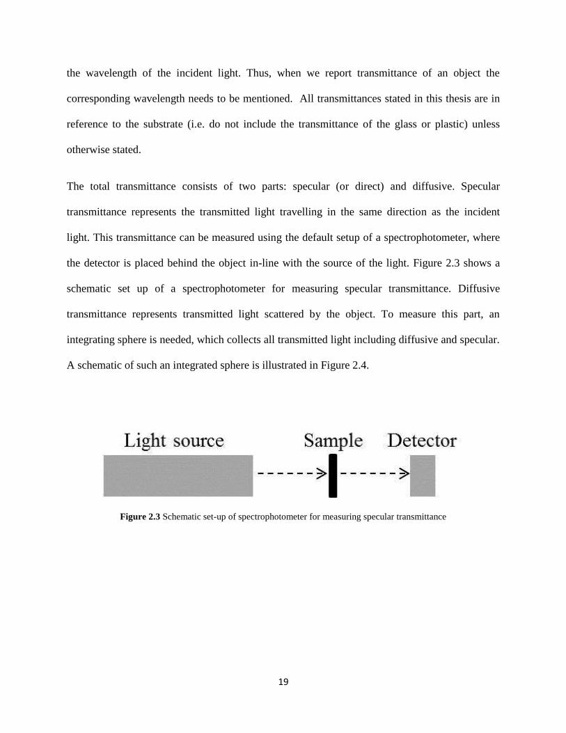
The total transmittance consists of two parts: specular (or direct) and diffusive. Specular
transmittance represents the transmitted light travelling in the same direction as the incident
light. This transmittance can be measured using the default setup of a spectrophotometer, where
the detector is placed behind the object in-line with the source of the light. Figure 2.3 shows a
schematic set up of a spectrophotometer for measuring specular transmittance. Diffusive
transmittance represents transmitted light scattered by the object. To measure this part, an
integrating sphere is needed, which collects all transmitted light including diffusive and specular.
A schematic of such an integrated sphere is illustrated in Figure 2.4.
Figure 2.3 Schematic set-up of spectrophotometer for measuring specular transmittance

20
Figure 2.4 Schematic set up of using an integrated integrating sphere to measure both diffusive and specular
transmittance [50]
For samples such as plain glass and ITO electrodes, diffusive transmittance is not significant
since they do not scatter light. However, silver nanowire electrodes do scatter a portion of the
incident light. Although scattered light results in hazy-looking electrodes, which are not good for
display applications, these electrodes can benefit solar cell applications by increasing the path
length of the incoming light, thereby increasing absorption and efficiency.
2.1.3 Sheet resistance
Resistivity is one of the elementary parameters of a conducting material. The symbol ρ with the
unit Ω•cm represents the resistivity of a material. Resistance is related to resistivity through:
,
where L is the length of the sample, and W and t are the width and thickness of the sample. Since
the thicknesses of films are often difficult to measure, sheet resistance is defined to represent
resistance per square area of a thin film with the unit Ω/ (Ohms per square) and is given by

21
So,
Thus, the total resistance of a film is proportional to the number of squares that can be drawn on
the conducting surface area. Figure 2.5 shows a top view of two typical resistors with the same
sheet resistance. Although their sizes are different, the numbers of drawn squares are equal.
Thus, the total resistance for both resistors would be the same.
Figure 2.5 Two resistors with the same sheet resistance and total resistance [51]
2.2 Fabrication of silver nanowire transparent electrodes
Silver nanowires dispersed in ethanol were purchased from Blue Nano Inc, with an average
diameter of 90nm and average length of 25 μm. The solution of nanowires needs to be deposited
uniformly on a substrate. Proper concentration was found by diluting initial the as-received
concentration (10 mg/ml) into various lower concentrations and depositing them on the glass
substrates (Microscope cover glass purchased from Fisher Scientific, Inc). The 5 mg/ml solution

22
is illustrated in Figure 2.6, and of those tested it provides the best uniformity and sheet resistance
on the substrates.
Figure 2.6 Silver nanowires solution with concentration of 5 mg/ml
Mayer rod size-10 and 20 were purchased from R. D. Specialities Inc. The size of the Mayer rod
represents the thickness of the deposited wet film. Uniformity of the deposited layer was better
for Mayer rod size 10, which made a wet layer with a thickness of 22.86 microns. Thus, 51
microliters of the solution is enough to make a layer of coating that covers the entire surface of a
50mm × 45 mm substrate. The required solution was dropped along one side of the substrate
using a pipette, and then the Mayer rod was rolled from one side to the other to distribute the
solution uniformly over the entire surface. Figure 2.7 illustrates the Mayer rod coating process
schematically and realistically.
Figure 2.7 (a) Schematic illustration of the Mayer rod coating method [52], (b) Mayer rod and glass substrates for
fabrication of transparent electrode

23
The coated layer was dried in air for 5 minutes. Additional layers can be deposited after the first
layer to reduce the sheet resistance. Desired sheet resistance and optical transmittance can be
achieved by controlling the number of deposited layers. After deposition, the resistance of the
films was high because the overlapping nanowires were not in good contact with one another.
Therefore, the films were annealed to fuse the overlapping nanowire junctions, which greatly
reduced the sheet resistance. After testing several annealing temperatures and times, it was
found that annealing at 200 °C for 30 minutes resulted in the lowest resistance. Higher
temperatures or longer times caused the nanowires to break up and thus resulted in lower
resistances. After the annealing step, two strips of copper tape were applied to the two ends of
each electrode to facilitate measurement of the electrode’s resistance. Figure 2.8 illustrates an
electrode that has 4 deposited nanowire layers with a sheet resistance of 12 Ω/ and 91%
transmittance at 550nm.
Figure 2.8 (a) Fabricated silver nanowire transparent electrode (b) SEM image of silver nanowire film on glass
substrate

24
2.3 Characterization of silver nanowire transparent electrodes
2.3.1 Transmittance and sheet resistance
The most critical characteristics of a transparent electrode are its sheet resistance and
transmittance. Sheet resistance of the electrode can be measured with either a 4-point probe
machine or a multimeter. In the latter method, sheet resistance is calculated by multiplying
measured resistance by the width to length ratio (W/l), according to the definition of sheet
resistance. For instance, resistance of the sample in Figure 2.8a is measured as 7.6 Ω and the
W/L ratio is 1.57. Thus, its sheet resistance is 12 Ω/. Both methods were used on several
samples and resulting sheet resistances were very similar.
Transmittance of the electrode was measured with a UV-2501PC Shimadzu spectrophotometer.
Specular transmittance can be measured using the default spectrophotometer setup. However, an
integrated sphere is needed to measure both specular and diffusive transmittances. Two samples
with various sheet resistances and transmittances were prepared by controlling the number of
deposited layers, and both their specular and their diffusive and specular (total) transmittances
were measured for comparison. Figure 2.9 shows spectra of the samples with various sheet
resistances either including (Figure 2.9a) or excluding their substrates (Figure 2.9b). A higher
concentration of silver nanowires on the substrates results in lower sheet resistance and
transmittance. In addition, as illustrated in Figure 2.9a, higher concentration leads to more
scattering of the incident light. In this case, the sample with sheet resistance of 65 Ω/ scatters
about 6% of the incident light. However, this amount increases to more than 10% for the sample
with sheet resistance of 12 Ω/. This is because the lower resistance electrode has a higher
density of nanowires, and thus scatters more.

25
Figure 2.9 (a) Transparency vs. wavelength of two silver nanowire transparent electrodes including the glass
substrates (transmittance of the plain glass is 91% at 550nm) (b) Transparency (specular + diffusive) of the
electrodes excluding the glass substrate (glass is used as a reference)
2.3.2 Data comparison
As mentioned, several alternatives have been introduced for ITO replacement. Figure 2.10
compares the characteristics of my silver nanowire electrodes with that of some of the alternative
materials and commercial ITO. Because high transparency and low resistance is desired, the
closer the data points are to the top left corner, the better. Results indicate that the silver
(specular + diffusive)
(specular)

26
nanowire transparent electrodes have better performance than the competing alternative materials
and match or are very close to commercial ITO.
Figure 2.10 Transparency versus sheet resistance for several transparent electrode materials. The data for the silver
nanowire electrodes are from my own experiments and references for the remainder of the data in the plot is from
[53]–[57].
2.3.3 Cost of silver nanowire films
Silver is an expensive metal, however, the amount of the silver that is used for fabrication of a
silver nanowire electrode is not significant. The price of pure silver is about $0.4 for the amount
of silver used in one meter square of an electrode with a sheet resistance of 10 Ω/ and 91%
transmittance at 550 nm. Because additional reactants, like ethylene glycol, are required to
synthesize silver nanowires, the cost to produce silver nanowires is more than the cost of silver
alone. The material cost of silver nanowire films with the same resistance and transparency as
stated above using commercial silver nanowire solutions (eg. from Blue Nano Inc.) is about $80
per meter square. However, if the nanowire solution is produced in the lab, the cost of silver

27
nanowire synthesis is $32.58/g and thus, the material cost of the films would be $12 per meter
square for a 10 Ω/ electrode, and less for electrodes with higher sheet resistances.
2.4 Flexibility of silver nanowire electrodes
Silver nanowires need to be deposited on a plastic substrate, such as PET or PEN, to enable
flexible transparent electrodes. PET films with 700 gauge (178 μm) thickness were purchased
from Dupont Teijin Films Inc. A solution of silver nanowires was deposited on the PET film as
described in the fabrication section. The electrodes were annealed at 100 ᵒC for 30 min since
higher temperature can damage the PET substrate. Because this annealing temperature was lower
than the ideal temperature, the nanowire junctions were not well fused and the sheet resistance of
the PET electrodes was higher than that of glass after annealing. To reduce the sheet resistance,
the PET electrodes were pressed in a mechanical press. Several electrodes were prepared in the
same manner, and pressures of 10 MPa, 20 MPa, 30 MPa and 40 MPa were applied to the
different electrodes. It was determined that 30 MPa resulted in the lowest sheet resistances. A
film of silver nanowires with a sheet resistance of 9 Ω/ and transmittance of 91% at 550 nm
was fabricated with this method, which is almost the same performance as the annealed silver
nanowire films on the glass substrates. To the best of our knowledge, this is the best performance
of flexible silver nanowire electrodes.
Several papers have shown the flexibility of silver nanowire transparent electrodes [58–60]. The
sheet resistance of spray coated and patterned silver nanowire transparent electrodes increased
more than 30% under a 120ᵒ and 140ᵒ bending angle, respectively [58-59]. However, our
samples show only 0-5% increase in sheet resistance under 140ᵒ bending angle and with bending
radius of 10 mm as it is illustrated in Figure 2.11. Once the sample is returned to its original flat

28
state, the resistance returns to its original value. Moreover, the sheet resistance did not change
after bending 100 times. It can be concluded that the PET silver nanowire electrodes are
promising for flexible electronics.
Figure 2.11 Resistance changes of flexible silver nanowire transparent electrode under a 140ᵒ bending angle (10
mm bending radius).
2.5 Surface roughness
As discussed in the Chapter 1, high surface roughness of silver nanowire electrodes is a major
problem. Atomic force microscopy (AFM) was used to measure the roughness of an as-deposited
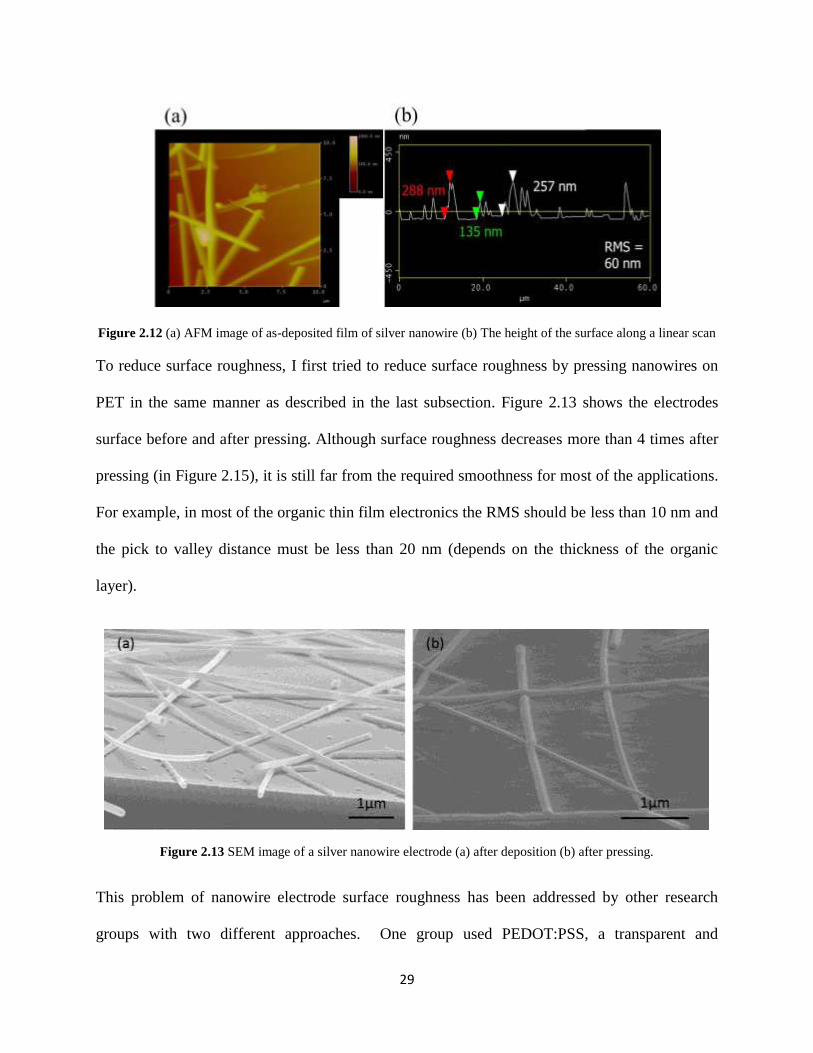
silver nanowire electrode. The RMS (Root Mean Square) surface roughness was 60nm over 10
μm × 10 μm area. Figure 2.12b shows the height of the surface along a linear scan. At some
points, there are 3 nanowires on top of one another and since the nanowires have a diameter of
90 nm, the maximum peak-to-valley height was nearly 300 nm.
29
Figure 2.12 (a) AFM image of as-deposited film of silver nanowire (b) The height of the surface along a linear scan
To reduce surface roughness, I first tried to reduce surface roughness by pressing nanowires on
PET in the same manner as described in the last subsection. Figure 2.13 shows the electrodes
surface before and after pressing. Although surface roughness decreases more than 4 times after
pressing (in Figure 2.15), it is still far from the required smoothness for most of the applications.
For example, in most of the organic thin film electronics the RMS should be less than 10 nm and
the pick to valley distance must be less than 20 nm (depends on the thickness of the organic
layer).
Figure 2.13 SEM image of a silver nanowire electrode (a) after deposition (b) after pressing.
This problem of nanowire electrode surface roughness has been addressed by other research
groups with two different approaches. One group used PEDOT:PSS, a transparent and

30
conductive polymer, to fill the spaces between the nanowires [61]. Surface roughness was
successfully reduced, however, because of the high roughness of the nanowire film a
PEDOT:PSS thickness of more than 125 nm is required. At these thicknesses there is a
significant reduction in transparency due to the limited transparency of the conductive polymer.
The second approach is to deposit a non-conductive but transparent polymer on top of the
nanowire electrode, and then peeling off the polymer-nanowire composite [62].The
manufacturing of this method would be complex and costly, however.
I developed a new method to reduce the surface roughness of silver nanowire electrodes which
do not have the drawbacks mentioned in the previous paragraph. Like the second method
mentioned, I used a transparent and non-conductive soft polymer, either SU-8 or PMMA, to fill
the space between the nanowires. However, instead of depositing the polymer on top of the
nanowire electrode, the nanowire film was instead pressed into the soft polymer. The nanowire
film was embedded into the top surface of the polymer and thus the polymer did not have to be
conductive, nor did the polymer-nanowire composite have to be peeled off the substrate.
Because I was not restricted to using a conductive polymer, this allowed me to select a polymer
that was much more transparent than a conducting polymer such as PEDOT:PSS. A SU-8 layer
with thickness of 1mm has more than 95% transmittance at 550nm [63].
In this method, a soft polymer layer was spin coated onto a substrate, and then the coated film
was placed on a hot plate slightly below the baking temperature of the polymer. Thus, the coated
polymer was neither soft nor completely hard. In this condition, silver nanowires were deposited
on the substrate and then pressed in a mechanical press with a pressure of 30 MPa. Figure 2.14
shows the schematic of this process. This process results in embedding silver nanowires into the
polymer and reducing surface roughness dramatically

31
Figure 2.14 Schematic of the embedding process of silver nanowires into a soft polymer film
Figure 2.15 shows AFM results for the pressed sample versus embedded nanowires. This surface
is smooth enough for many applications even though further optimization is needed to decrease
the roughness further to reach to the required roughness for thinner devices.
Figure 2.15 AFM image of pressed film of silver nanowire (left), and embedded silver nanowires on a soft polymer
(right)
2.6 Device integration
I used the fabricated silver nanowire electrodes in different devices and applications. In Chapter
4, silver nanowire electrodes are used as transparent heaters, which is a new application of these
electrodes. Moreover, the electrodes were used in organic solar cells as the anode layer at the top
of an inverted device as illustrated in figure 2.16. Leanne Murphy, a Master’s student from
Chemical Engineering department of the University of Waterloo helped me to make the device
and collected the required data. In this structure, light can be shone through both sides, which
32
can enhance the efficiency of the solar cells and open the possibility for partially transparent
solar cells which could be used on windows for example.
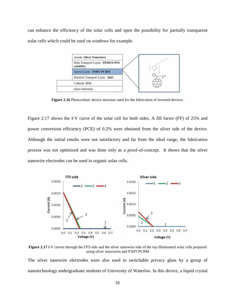
Figure 2.16 Photovoltaic device structure used for the fabrication of inverted devices.
Figure 2.17 shows the I-V curve of the solar cell for both sides. A fill factor (FF) of 25% and
power conversion efficiency (PCE) of 0.2% were obtained from the silver side of the device.
Although the initial results were not satisfactory and far from the ideal range, the fabrication
process was not optimized and was done only as a proof-of-concept. It shows that the silver
nanowire electrodes can be used in organic solar cells.
Figure 2.17 I-V curves through the ITO side and the silver nanowire side of the top illuminated solar cells prepared
using silver nanowires and P3HT/PCBM
The silver nanowire electrodes were also used in switchable privacy glass by a group of
nanotechnology undergraduate students of University of Waterloo. In this device, a liquid crystal
1 3 1
2
2
3

33
solution was injected between two pieces of glass coated with silver nanowire electrodes. The
transparency of the liquid crystal solution was altered by applying a voltage across the two
electrodes.

34
Chapter 3
Instability of silver nanowire transparent electrodes
under current flow
In this chapter, we show that when silver nanowire electrodes conduct the current at levels
encountered in organic solar cells, the electrodes can fail in as little as two days. Electrode
failure is caused by Joule heating which causes the nanowires to breakup and thus create an
electrical discontinuity in the nanowire film. More heat is created, and thus failure occurs sooner
in more resistive electrodes and at higher current densities. Suggestions to improve the stability
of silver nanowire electrodes are given. These results were summarized in a paper submitted in
March 2013 [98].
3.1. Introduction
There are numerous reports about the promising device characteristics of organic solar cells
using silver nanowire electrodes [64,65]. Silver nanowires are known to oxidize and corrode
over a period of months in air [66], however, there are no studies on the stability of the nanowire
electrodes during use (i.e. when they are conducting current). In contrast to ITO where current
conducts throughout the entire area of the film, in nanowire electrodes electronic transport occurs
only through the metal wire pathways, and these nanowire pathways have diameters less than
100 nm. Because of this, although the current densities generated in organic solar cells are
relatively low (on the order of 10 mA/cm2, with the best performing devices generating about 17
mA/cm2 [67]), the resulting current densities in the nanowires are very high. For example, if we
assume half the nanowires in 12 Ω/ silver nanowire electrodes participate in current
conduction, a solar cell current density of 17 mA/cm2 would result in an approximate current

35
density in the nanowires of 4×10⁴ A/cm
2 [68]. For comparison, this same current flowing
through a 250 nm thick ITO film results in a current density of 103 A/cm
2, more than an order of
magnitude less.
In this chapter, it is shown that at current density levels incurred in organic solar cells, silver
nanowire electrodes fail in a matter of days. We report how parameters such as sheet resistance
and current density affect the time to failure, as well as characterize the electrodes to investigate
the failure mechanism.
3.2. Experiment
Silver nanowires electrodes were fabricated and characterized as described in chapter 2. To
investigate the effects of current flow through the electrodes, a DC power supply was used to
pass a constant current across the electrodes. Current was conducted until the electrodes failed,
which we define as the point when the DC power supply reached its maximum of 30 V and thus
could no longer maintain the constant current. The voltage across the electrodes and the surface
temperature were monitored continuously throughout the experiment using computer data
collection. For the temperature measurement, a flat leaf-style thermocouple was used. The
electrodes were soon afterwards imaged with SEM, for which a thin coating of gold on the
sample was required to prevent electron charging. Transmission electron microscopy (TEM)
samples were prepared by mechanically rubbing the electrodes onto copper grids overlayed with
ultra-thin amorphous carbon. Both bright-field images and energy dispersive spectroscopy
(EDS) spectra were obtained in the TEM.
For comparison purposes, additional nanowire electrodes were prepared but no current was
passed across them. Rather, one electrode was left in air and its sheet resistance was monitored

36
over the period of one year. Other electrodes were annealed in an atmospheric furnace each at
various temperatures and times. These electrodes were imaged in the SEM at various stages to
see how the electrode morphology evolved throughout the annealing process.
3.3. Results and discussion
3.3.1 Electrode failure measurements
An SEM image of a prepared nanowire electrode is shown in Figure 3.1a. The transparency of
all electrodes was nearly constant across all visible wavelengths (Figure 2.9), as similarly found
by other groups [69,70,71]. The electrodes prepared for the stability experiments had sheet
resistances ranging from 12 Ω/ (with a corresponding transparency of 91% at a wavelength of
550 nm) to 37 Ω/ (with a transparency of 94% at 550 nm). Figure 3.1b shows the evolution of
the voltage and surface temperature of a 12 Ω/ nanowire electrode as 17 mA/cm2 of current was
passed across it. As was typical with all samples measured, the voltage (and therefore resistance)
gradually increased with time, and then suddenly jumped to 30 V once the electrode failed. The
power dissipated in the electrode is P = IV, so with a constant current and a gradually increasing
voltage, the surface temperature gradually increased over time as well until electrode failure.
Figure 3.1 (a) SEM image of an as-prepared electrode. (b) Voltage and surface temperature of a 12 Ω/ sample
when a constant current density of 17 mA/cm2 was applied across the electrode

37
Figure 3.2a shows that under a constant current density, electrodes with a higher sheet resistance
fail more quickly. Higher sheet resistance electrodes have sparser nanowire networks, and thus
the current density in the individual nanowires is higher than in lower resistance electrodes.
Joule heating is also higher in more resistive films, since P = IV = I2R. The surface temperatures
immediately preceding electrode failure of the four samples measured for Figure 3.2a, from the
lowest to highest sheet resistance, was: 55 °C, 70 °C, 100 °C, and 102 °C.
Figure 3.2 (a) The number of days to failure versus sheet resistance, when conducting 17 mA/cm2 across samples
with different resistances. (b) The relationship between the number of days to failure and current density, as
measured with three different 30 Ω/ electrode
Figure 3.2b illustrates that for nanowire electrodes with the same sheet resistance, a higher
current density results in a shorter lifetime. Similar to above, a higher current density results in
higher currents through the individual nanowires and more Joule heating. The temperature of the
electrode preceding failure for the three current densities applied in Figure 3.2b, from lowest to
highest current density, was: 50 °C, 74 °C, and 100°C.
In the comparison sample, where a nanowire electrode was left in air without current flow, the
sheet resistance only increased by 10% after three months. After one year, however, the
resistance was 6 orders of magnitude higher than its original value.
38
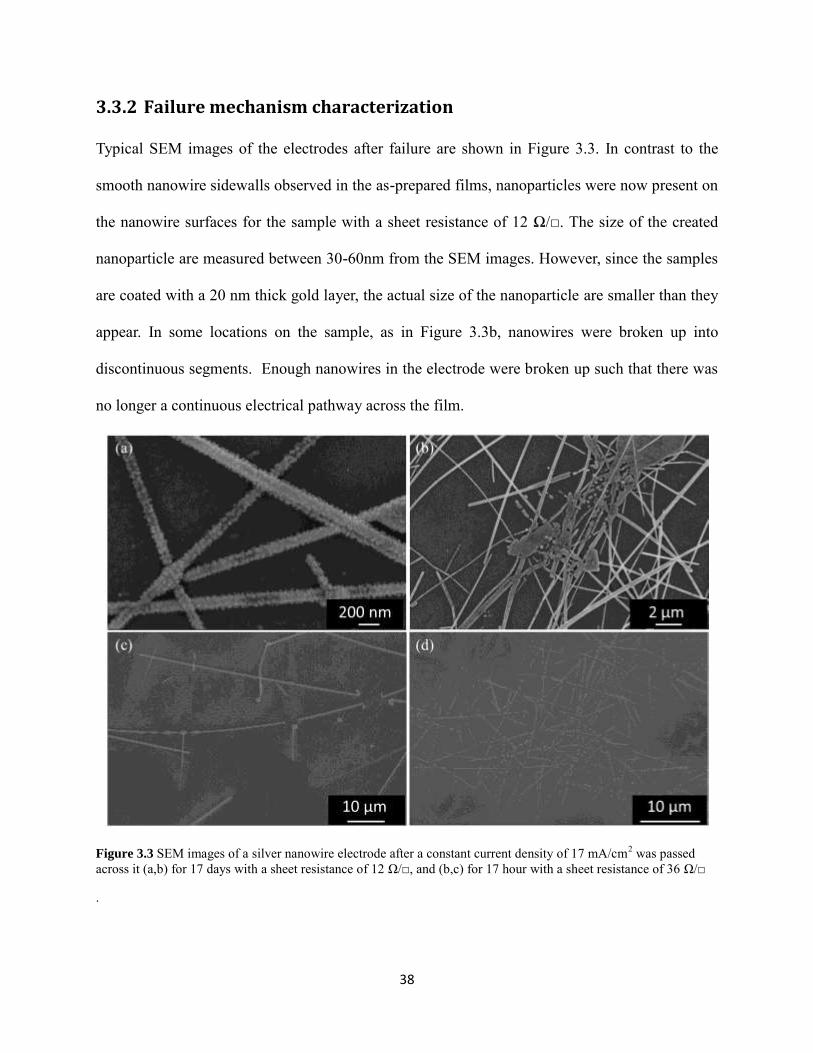
3.3.2 Failure mechanism characterization
Typical SEM images of the electrodes after failure are shown in Figure 3.3. In contrast to the
smooth nanowire sidewalls observed in the as-prepared films, nanoparticles were now present on
the nanowire surfaces for the sample with a sheet resistance of 12 Ω/. The size of the created
nanoparticle are measured between 30-60nm from the SEM images. However, since the samples
are coated with a 20 nm thick gold layer, the actual size of the nanoparticle are smaller than they
appear. In some locations on the sample, as in Figure 3.3b, nanowires were broken up into
discontinuous segments. Enough nanowires in the electrode were broken up such that there was
no longer a continuous electrical pathway across the film.
Figure 3.3 SEM images of a silver nanowire electrode after a constant current density of 17 mA/cm2 was passed
across it (a,b) for 17 days with a sheet resistance of 12 Ω/, and (b,c) for 17 hour with a sheet resistance of 36 Ω/
.

39
Figure 3.3 c and d shows SEM images of the electrode after failure with higher sheet resistance
under the same current density as the sample in Figure 3.3 a and b. In this case the shapes of the
nanowires are completely changed into spherical forms in some locations, which may be due to
the higher temperature resulting from the higher current density passing through individual
nanowires.
Although silver is susceptible to electromigration at the current densities and temperatures
encountered in these electrodes [72], the SEM images are not indicative of the voids and hillocks
that are characteristic of electromigration [11–14]. Rather, our study suggests that it is the
instability of nanowires at elevated temperatures which is the reason for the electrode failure. As
mentioned in the experimental section, nanowire electrodes were annealed at various
temperatures without current flow. Figure 3.4 shows SEM images of nanowire during annealing
for 17 days at 100 °C and 150 °C. Even at a temperature as low as 100 °C, nanoparticles formed
on the surfaces of the nanowires The samples annealed at 100 ᵒC were removed from the furnace
every few days to take images throughout the annealing process. The resulting images show that
the size and density of nanoparticles increased with increasing annealing time. At 150 °C,
nanoparticles also formed and the nanowires eventually broke up into discontinuous segments
(Figure 3.4d).

40
Figure 3.4 SEM images of silver nanowire electrodes annealed on a glass substrate for (a) 7 days, (b) 14 days, and
(c) 17 days at 100 °C, and for (d) 17 days at 150 °C.
In addition, silver nanowires were annealed at higher temperature for a short time to investigate
the effect of higher temperature on silver nanowire structures. Figure 3.5 shows optical
microscope images of the silver nanowires after annealing at 300 ᵒC for one and half hours. The
nanowire were melted or turned into spherical shapes after a short time.
Figure 3.5 silver nanowires annealed at 300 ᵒC (a) for half an hour (b) for one and half hour.

41
As noted in the section above, when current is passed through a nanowire electrode the
temperature is elevated due to Joule heating. Although the surface temperature of the electrodes
was around or below 100 °C while conducting current, the temperature of the nanowires
themselves are intuitively higher than the average surface temperature, particularly at the
resistive junctions where two nanowires overlap. The annealing experiments showed that
nanowire networks in air at modest temperatures are unstable; nanoparticles first form and then
the nanowires eventually break up and become electrically discontinuous. Thus, in the case of
current conduction, the temperature of the nanowires rise due to Joule heating and the instability
of the nanowires at these temperatures causes the electrodes to fail. Comparing the time to
failure of the 12 Ω/ electrode under 17 mA/cm2 of current flow to the time for the nanowires in
the annealed samples to breakup, we estimate the temperature of the nanowires themselves in
this particular case was between 100 and 150 °C. In addition, the resulting structures of the silver
nanowire, annealed at 300 °C, are similar to the 36 Ω/ silver nanowire electrodes under 17
mA/cm2 of current flow, which failed after 17 hours (Figure 3.3d).
Elechiguerra et al. found that silver nanowires synthesized by the polyol method corrode in the
atmosphere [77]. Rather than corroding by reacting with oxygen, silver corrodes due to reduced-
sulfur gases present in the air. They observed that after three weeks, silver sulfide (Ag2S)
nanoparticles started to form on the surface of the nanowires and after six months, some of the
nanowires became discontinuous. In our experiments, nanoparticles and breakage occur much
faster. Corrosion is greatly enhanced at elevated temperatures [16]. EDS spectra were taken
from the nanoparticles decorating the surface of the nanowires after electrode failure (Figure
3.6). Other than the carbon and copper signals originating from the TEM grid, only silver and
sulphur were detected. The ratio of silver to sulphur content was 9:1. The presence of sulphur

42
indicates that the electrodes may have failed due to the corrosion of the nanowires in the
atmosphere at the elevated temperatures caused by Joule heating.
Figure 3.6 Energy dispersive spectrum of a nanoparticle formed on a silver nanowire after electrode failure. The x
indicates the location where the measurement was taken. Sulfur was detected in the nanoparticles indicating
corrosion of the silver.
Alternatively, or addition to corrosion, another reason for the breakup of the silver nanowires at
increased temperatures could be attributed to the high surface energy of the nanowires.
Nanowires have a large surface-area-to-volume ratio, and the sidewalls of the nanowires used in
the electrodes are all 110 planes [79], which are not the lowest energy planes in an FCC
material. At elevated temperatures, atomic diffusion is increased and kinetic limitations to
reconstruction can be overcome. Silver nanobelts and nanowires of other metals have been
shown to fragment at temperatures far below their bulk melting temperatures due to Rayleigh
instability [80], [81] and a similar phenomenon may be occurring here.
3.3.3 Relevance to nanowire electrode design
The experimental results indicate that steps must be taken to improve the longevity of nanowire
electrodes under current flow before they are suitable for use in organic solar cells. In a flexible
organic solar cell, the substrate underneath the transparent electrode is typically a plastic such as
polyethylene terephthalate (PET) or polyethylene naphthalate (PEN), and organic materials are

43
deposited on top of the electrode. PET and PEN are permeable to gas [82], as are many of the
common small molecules or polymeric materials in organic solar cells [83], and so these
materials will likely not prevent corrosion. Researchers are developing organic solar cell
materials with low permeability to gas [84,85]. Alternatively, encapsulation of the organic solar
cell [86,87] may prevent the corrosion of the silver nanowire electrode. Another option is to
passivate the silver nanowires with a conductive coating. Ahn et al. showed that a graphene
oxide coating, which is impermeable to gas molecules, reduced, but did not completely prevent,
the increase of sheet resistance of silver nanowire electrodes when annealed at 70 °C in high
humidity over one week [88]. A better passivation will likely be required.
Larger diameter nanowires would take longer to corrode, and also have smaller surface-area-to-
volume ratios and would thus be more stable at elevated temperatures. Another potentially
helpful strategy would be to synthesize and deposit films of silver nanowires which have low
energy 111 facets. Also, alternative metallic nanowires that are less susceptible to corrosion
could be considered, such as cupronickel nanowires [89]. Our results also indicate the
importance of keeping current densities low and using low resistance nanowire electrodes, which
are unfortunately less transparent.
3.4. Conclusions
The data in this chapter shows that at current levels generated in organic solar cells, silver
nanowire electrodes fail in an unacceptably short time. Electrodes with higher sheet resistances,
and electrodes subject to higher current densities, fail more quickly. The reason for electrode
failure is attributed to elevated temperatures caused by Joule heating. Design factors such as
passivation, electrode sheet resistance, and nanowire diameter need to be considered before
silver nanowire electrodes will be useful as an ITO replacement in organic solar cells.

44
Chapter 4
Silver nanowire transparent heaters
In this chapter, silver nanowire transparent heaters are introduced as a new application of silver
nanowire electrodes. The performance and characterization of the transparent heaters are
illustrated and compared with conventional transparent heaters and other new alternatives. We
show that the heating performance of silver nanowire heaters is better than those of ITO and
CNT heaters, lower power is required to reach to the same surface temperature. Moreover, a
voltage as low as 6 V heats the surface up to 100 ᵒC.
4.1 Introduction
Transparent heater films have applications in many areas such as window defrosters, maintaining
the required temperature for liquid crystal display operation, goggle defrosters, and various
military and medical applications. ITO thin film heaters are commercially available on the
market. However, as mentioned in previous chapters, because of the disadvantages of ITO like
high cost and brittleness, researchers are trying to introduce new transparent heaters based on
other materials such as graphene and carbon nanotubes [90–93].
In addition to their cost, flexibility, and ease of fabrication, the thermal conductivity and power
consumption of the heaters are also critical characteristics that need to be considered. ITO has
low thermal conductivity in the order of 8-12 W/m•K [94]. In comparison, silver has a thermal
conductivity of 400-440 W/m•K which is 50 times higher than that of ITO [95]. The thermal
conductivity of CNT and graphene are about one order of magnitude higher than that of silver,
and this high conductivity results in fast heating and cooling [95]. However, if a higher surface
temperature is required, the higher sheet resistance of graphene and CNT films necessitates that a

45
higher voltage be applied or that a film with a low transmittance (and therefore lower resistance)
be used. Such is not the case with silver nanowire electrodes. A heater’s performance is
determined by calculating its power consumption for generating a particular surface temperature.
A high performance heater needs less power to reach the required surface temperature.
Silver nanowire transparent electrodes not only have relatively high thermal conductivity but
also have low sheet resistance and high transmittance. Thus, transparent heaters based on silver
nanowires can perform with very low voltages and provide high transmittance. Recently,
fabrication of silver nanowire transparent heaters has been reported elsewhere [96], which
preempted our efforts to publish the first report on this application but confirmed our results.
4.2 Experiment setup
Transparent electrodes with various sheet resistances were fabricated either on PET or glass
substrates with the size of 40 mm × 50 mm, as described in Chapter 2. For the PET samples, a
pressure of 30 MPa was applied to enhance the sheet resistance of the films, as mentioned in
Chapter 2. Figure 4.1 shows the schematic of experimental setup. A flat leaf-style thermocouple
was attached to the backside of the substrate (opposite side from the nanowire film) and the
temperature data was collected using a digital thermometer connected to a computer. The surface
temperature was recorded every second during the experiment. A constant voltage was applied
for 600 seconds across the copper strips using a DC power supply, creating a flowing current
which was also recorded. Then the power supply was disconnected from the electrode and
surface temperatures were still monitored to plot the cooling trend.

46
The total transmittance (specular and diffusive) of the films were measured using an integrating
sphere and a spectrophotometer, and the sheet resistances were measured using either a multi-
meter or 4-point probe system, as described in Chapter2.
Figure 4.1 Schematic setup of experiment for measuring the transparent heater performance
The power consumption was calculated using the following equation:
𝑃 𝑉2
where P is the power consumption in Watts, V is the applied voltage, and R is the film’s
resistance, which can be calculated by dividing the voltage by the recorded current. The equation
indicates that for the same power consumption, a lower sheet resistance results in lower required
voltage. Power densities were calculated for each sample by dividing the calculated power by the
surface area of the heater.
4.3 Results and discussion
Heating and cooling trends of the silver nanowire transparent heaters under various applied
voltages, on PET and glass substrates, are shown in Figure 4.2. This figure shows that almost all
of the heaters reach their steady state temperature after 200 seconds. In addition, Figure 4.2a
shows that the surface temperature of the heater on a PET or a glass substrate reached about 80
ᵒC with a low voltage of 6 V. For comparison, the surface temperature of ITO and CNT film
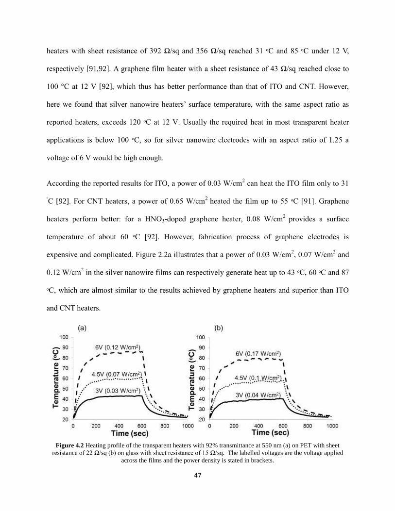
47
heaters with sheet resistance of 392 Ω/sq and 356 Ω/sq reached 31 ᵒC and 85 ᵒC under 12 V,
respectively [91,92]. A graphene film heater with a sheet resistance of 43 Ω/sq reached close to
100 °C at 12 V [92], which thus has better performance than that of ITO and CNT. However,
here we found that silver nanowire heaters’ surface temperature, with the same aspect ratio as
reported heaters, exceeds 120 ᵒC at 12 V. Usually the required heat in most transparent heater
applications is below 100 ᵒC, so for silver nanowire electrodes with an aspect ratio of 1.25 a
voltage of 6 V would be high enough.
According the reported results for ITO, a power of 0.03 W/cm2 can heat the ITO film only to 31
ᵒC [92]. For CNT heaters, a power of 0.65 W/cm
2 heated the film up to 55 ᵒC [91]. Graphene
heaters perform better: for a HNO3-doped graphene heater, 0.08 W/cm2
provides a surface
temperature of about 60 ᵒC [92]. However, fabrication process of graphene electrodes is
expensive and complicated. Figure 2.2a illustrates that a power of 0.03 W/cm2, 0.07 W/cm
2 and
0.12 W/cm2 in the silver nanowire films can respectively generate heat up to 43 ᵒC, 60 ᵒC and 87
ᵒC, which are almost similar to the results achieved by graphene heaters and superior than ITO
and CNT heaters.
Figure 4.2 Heating profile of the transparent heaters with 92% transmittance at 550 nm (a) on PET with sheet
resistance of 22 Ω/sq (b) on glass with sheet resistance of 15 Ω/sq. The labelled voltages are the voltage applied
across the films and the power density is stated in brackets.
48
As illustrated in Figure 4.2, the PET substrate heater reaches higher temperature with lower
power consumption than glass substrates with the same thickness, meaning that PET substrate
heaters perform better. The power densities vs. maximum surface temperature were plotted for
the PET and the glass substrates for different sheet resistances, as shown in Figure 4.3. This
figure confirms that for the same power density, PET heaters reach higher surface temperature.
This behavior might be due to the difference in thermal conductivity of the substrates; glass
thermal conductivity is about five times greater than that of PET [96,97]. Thus, heat is
transferred slower in PET, resulting in higher surface temperature.
Figure 3 also shows that for the same input power, the maximum temperature at a given power
density is higher for heaters with higher sheet resistance. We know that higher sheet resistance is
a consequence of a lower concentration of silver nanowires. Therefore, for a given input power,
each nanowire dissipates more power. According to the following thermodynamic equation,
higher power consumption results in a bigger temperature change
𝑄 𝑚𝑐∆𝑇
where Q is the consumed energy in Joules, and m and c are the mass of the nanowire and specific
heat capacity of silver, respectively. For the same power input to a sample with low sheet
resistance (due to a higher concentration of nanowires), the change in temperature of each
individual nanowire would be smaller.
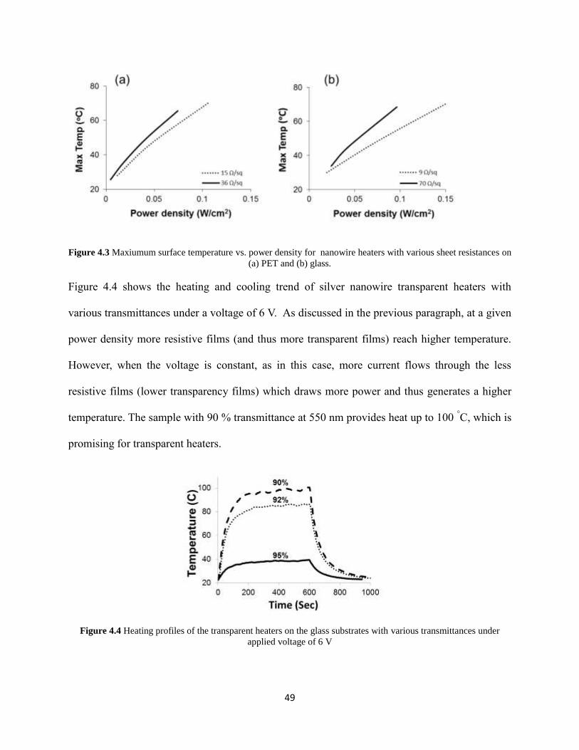
49
Figure 4.3 Maxiumum surface temperature vs. power density for nanowire heaters with various sheet resistances on
(a) PET and (b) glass.
Figure 4.4 shows the heating and cooling trend of silver nanowire transparent heaters with
various transmittances under a voltage of 6 V. As discussed in the previous paragraph, at a given
power density more resistive films (and thus more transparent films) reach higher temperature.
However, when the voltage is constant, as in this case, more current flows through the less
resistive films (lower transparency films) which draws more power and thus generates a higher
temperature. The sample with 90 % transmittance at 550 nm provides heat up to 100 °C, which is
promising for transparent heaters.
Figure 4.4 Heating profiles of the transparent heaters on the glass substrates with various transmittances under
applied voltage of 6 V
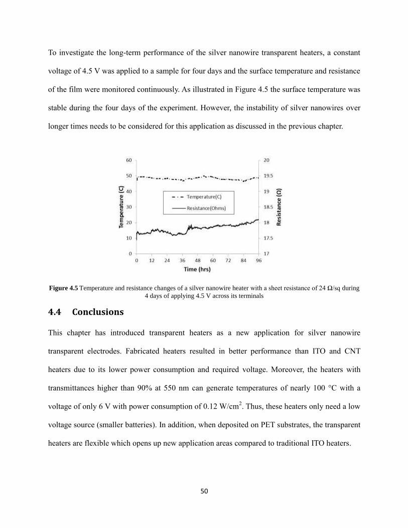
50
To investigate the long-term performance of the silver nanowire transparent heaters, a constant
voltage of 4.5 V was applied to a sample for four days and the surface temperature and resistance
of the film were monitored continuously. As illustrated in Figure 4.5 the surface temperature was
stable during the four days of the experiment. However, the instability of silver nanowires over
longer times needs to be considered for this application as discussed in the previous chapter.
Figure 4.5 Temperature and resistance changes of a silver nanowire heater with a sheet resistance of 24 Ω/sq during
4 days of applying 4.5 V across its terminals
4.4 Conclusions
This chapter has introduced transparent heaters as a new application for silver nanowire
transparent electrodes. Fabricated heaters resulted in better performance than ITO and CNT
heaters due to its lower power consumption and required voltage. Moreover, the heaters with
transmittances higher than 90% at 550 nm can generate temperatures of nearly 100 °C with a
voltage of only 6 V with power consumption of 0.12 W/cm2. Thus, these heaters only need a low
voltage source (smaller batteries). In addition, when deposited on PET substrates, the transparent
heaters are flexible which opens up new application areas compared to traditional ITO heaters.
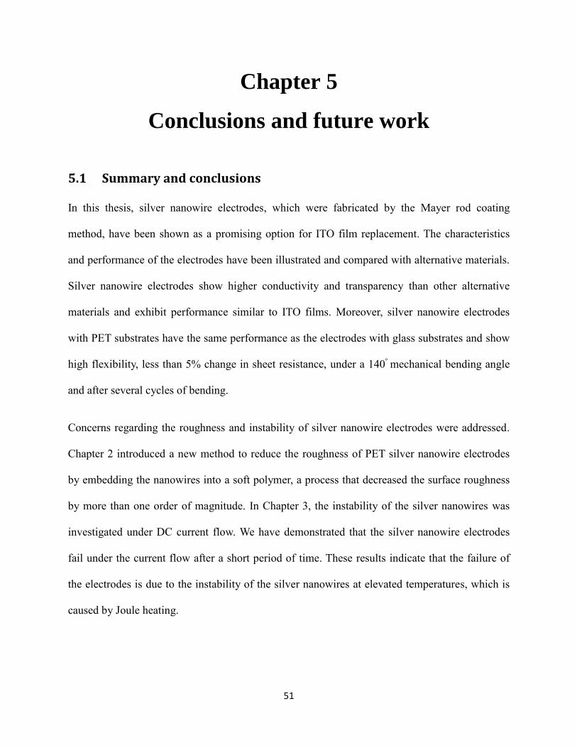
51
Chapter 5
Conclusions and future work
5.1 Summary and conclusions
In this thesis, silver nanowire electrodes, which were fabricated by the Mayer rod coating
method, have been shown as a promising option for ITO film replacement. The characteristics
and performance of the electrodes have been illustrated and compared with alternative materials.
Silver nanowire electrodes show higher conductivity and transparency than other alternative
materials and exhibit performance similar to ITO films. Moreover, silver nanowire electrodes
with PET substrates have the same performance as the electrodes with glass substrates and show
high flexibility, less than 5% change in sheet resistance, under a 140ᵒ mechanical bending angle
and after several cycles of bending.
Concerns regarding the roughness and instability of silver nanowire electrodes were addressed.
Chapter 2 introduced a new method to reduce the roughness of PET silver nanowire electrodes
by embedding the nanowires into a soft polymer, a process that decreased the surface roughness
by more than one order of magnitude. In Chapter 3, the instability of the silver nanowires was
investigated under DC current flow. We have demonstrated that the silver nanowire electrodes
fail under the current flow after a short period of time. These results indicate that the failure of
the electrodes is due to the instability of the silver nanowires at elevated temperatures, which is
caused by Joule heating.

52
The electrodes have also been integrated in different electronic devices, including transparent
heaters, organic solar cells, and switchable privacy glass. In Chapter 4, silver nanowire
transparent heaters are introduced as a new application of the silver nanowire electrodes. The
fabricated heaters perform better than the ITO and CNT heaters, consume less power to reach the
same surface temperature and need low applied voltage. The effect of sheet resistance on the
performance of these heaters is also discussed in this chapter. The surface temperature of a silver
nanowire heater with 90% transmittance at 550 nm wavelength, reached to 100ᵒ C under an
applied voltage of 6V
5.2 Future work
The study of silver nanowires and fabricated transparent electrodes can proceed in several
directions. I suggest a few important directions here. Firstly, further investigation should be
done on the instability of the solution-synthesized silver nanowires and possible ways to make
them more stable. We need methods of passivating the surfaces of silver nanowires with
conductive films so that the electrodes can operate over long lifetimes. Secondly, the silver
nanowire electrodes can be integrated in and optimized for various electronic devices. For
example, it is likely that the performance of organic solar cells using nanowire electrodes can be
improved by optimizing the fabrication process. Thirdly, although I presented a method to reduce
the surface roughness of the electrodes, for some applications the roughness needs to be reduced
further so an optimization of my process or a different process should be investigated.

53
References
[1] F. Yakuphanoglu and R. S. Anand, “Charge transport properties of an organic solar cell,”
Syn. Met, vol. 160, no. 21, pp. 2250–2254, 2010.
[2] http://www.dmccoltd.com/english/tecnical/logs/images/tec20041126_a_1.gif.
[3] http://news.thomasnet.com/fullstory/Transparent-Heater-utilizes-ITO-technology-27584.
[4] D. S. Ginley, Handbook of Transparent Conductors. Springer, 2010.
[5] B. Zhang, X. Dong, X. Xu, X. Wang, and J. Wu, “Electrical and optical properties of ITO
and ITO: Zr transparent conducting films,” Mat. Sci. Semicon. Proc. , vol. 10, no. 6, pp.
264–269, 2007.
[6] S. H. Mohamed, F. M. El-Hossary, G. A. Gamal, and M. M. Kahlid, “Properties of Indium
Tin Oxide thin films deposited on polymer substrates,” Acta Phys. Polonica A, vol. 115, no.
3, pp. 704–708, 2009.
[7] Fenn J, “If not ITO, then what?” presented at Soc. Vac. Coat., 2010.
[8] D. R. Cairns, D. K. Sparacin, D. C. Paine, and G. P. Crawford, “19.3: Electrical Studies of
Mechanically Deformed Indium Tin Oxide Coated Polymer Substrates,” in SID
Symposium Digest of Technical Papers, 2012, vol. 31, pp. 274–277.
[9] D. S. Hecht, L. Hu, and G. Irvin, “Emerging Transparent Electrodes Based on Thin Films
of Carbon Nanotubes, Graphene, and Metallic Nanostructures,” Adv. Mat., vol. 23, no. 13,
pp. 1482–1513, Apr. 2011.
[10] S. Iijima and T. Ichihashi, “Single-shell carbon nanotubes of 1-nm diameter,” Nature, vol.
363, no. 6430, pp. 603–605, Jun. 1993.

54
[11] M. S. Fuhrer, J. Nygård, L. Shih, M. Forero, Y. G. Yoon, M. S. C. Mazzoni, H. J. Choi, J.
Ihm, S. G. Louie, A. Zettl, and P. L. McEuen, “Crossed Nanotube Junctions,” Science, vol.
288, no. 5465, pp. 494–497, Apr. 2000.
[12] S. Xie, W. Li, Z. Pan, B. Chang, and L. Sun, “Mechanical and physical properties on
carbon nanotube,” Phy. Chem. Sol, vol. 61, no. 7, pp. 1153–1158, Jul. 2000.
[13] X. Wan, J. Dong, and D. Y. Xing, “Optical properties of carbon nanotubes,” Phys. Rev. B,
vol. 58, no. 11, pp. 6756–6759, Sep. 1998.
[14] “http://www.ppr3.go.th/carbon-nanotubes-images&page=3.”
[15] B. Dan, G. C. Irvin, and M. Pasquali, “Continuous and scalable fabrication of transparent
conducting carbon nanotube films,” ACS Nano, vol. 3, no. 4, pp. 835–843, 2009.
[16] D. S. Hecht, A. M. Heintz, R. Lee, L. Hu, B. Moore, C. Cucksey, and S. Risser, “High
conductivity transparent carbon nanotube films deposited from superacid,”
Nanotechnology, vol. 22, no. 7, p. 075201, 2011.
[17] Z. Wu, “Transparent, Conductive Carbon Nanotube Films,” Science, vol. 305, no. 5688, pp.
1273–1276, Aug. 2004.
[18] P. N. Nirmalraj, P. E. Lyons, S. De, J. N. Coleman, and J. J. Boland, “Electrical
Connectivity in Single-Walled Carbon Nanotube Networks,” Nano Lett, vol. 9, no. 11, pp.
3890–3895, 2009.
[19] Z. Li, H. R. Kandel, E. Dervishi, V. Saini, A. S. Biris, A. R. Biris, and D. Lupu, “Does the
wall number of carbon nanotubes matter as conductive transparent material?,” App. Phy.
Lett, vol. 91, no. 5, p. 053115, 2007.

55
[20] D.-W. Shin, J. H. Lee, Y.-H. Kim, S. M. Yu, S.-Y. Park, and J.-B. Yoo, “A role of HNO3
on transparent conducting film with single-walled carbon nanotubes,” Nanotechnology, vol.
20, no. 47, p. 475703, 2009.
[21] H. Z. Geng, K. K. Kim, K. P. So, Y. S. Lee, Y. Chang, and Y. H. Lee, “Effect of acid
treatment on carbon nanotube-based flexible transparent conducting films,” J. Am. Chem.
Soc, vol. 129, no. 25, pp. 7758–7759, 2007.
[22] N. Saran, K. Parikh, D. S. Suh, E. Munoz, H. Kolla, and S. K. Manohar, “Fabrication and
characterization of thin films of single-walled carbon nanotube bundles on flexible plastic
substrates,” J. Am. Chem. Soc, vol. 126, no. 14, pp. 4462–4463, 2004.
[23] B. B. Parekh, G. Fanchini, G. Eda, and M. Chhowalla, “Improved conductivity of
transparent single-wall carbon nanotube thin films via stable postdeposition
functionalization,” Appl. Phys. Lett, vol. 90, no. 12, p. 121913, 2007.
[24] C. M. Trottier, P. Glatkowski, P. Wallis, and J. Luo, “Properties and characterization of
carbon-nanotube-based transparent conductive coating,” J. Soc. Info. Displ, vol. 13, no. 9,
pp. 759–763, 2005.
[25] A. A. Green and M. C. Hersam, “Solution Phase Production of Graphene with Controlled
Thickness via Density Differentiation,” Nano Lett, vol. 9, no. 12, pp. 4031–4036, Dec.
2009.
[26] K. S. Novoselov, A. K. Geim, S. V. Morozov, D. Jiang, Y. Zhang, S. V. Dubonos, I. V.
Grigorieva, and A. A. Firsov, “Electric Field Effect in Atomically Thin Carbon Films,”
Science, vol. 306, no. 5696, pp. 666–669, 2004.
56
[27] H. C. Schniepp, K. N. Kudin, J.-L. Li, R. K. Prud’homme, R. Car, D. A. Saville, and I. A.
Aksay, “Bending Properties of Single Functionalized Graphene Sheets Probed by Atomic
Force Microscopy,” ACS Nano, vol. 2, no. 12, pp. 2577–2584, 2008.
[28] X. Wang, L. Zhi, and K. Müllen, “Transparent, Conductive Graphene Electrodes for Dye-
Sensitized Solar Cells,” Nano Lett, vol. 8, no. 1, pp. 323–327, 2008.
[29] A. N. Obraztsov, “Chemical vapour deposition: Making graphene on a large scale,” Nat.
Nano, vol. 4, no. 4, pp. 212–213, 2009.
[30] “http://www.fujitsu.com/downloads/EDG/binary/pdf/find/26-1e/11.pdf,” organic
conducting polymers.
[31] W. Hong, Y. Xu, G. Lu, C. Li, and G. Shi, “Transparent graphene/PEDOT–PSS composite
films as counter electrodes of dye-sensitized solar cells,” Electrochem. Commun, vol. 10,
no. 10, pp. 1555–1558, 2008.
[32] J. Zou, H.-L. Yip, S. K. Hau, and A. K.-Y. Jen, “Metal grid/conducting polymer hybrid
transparent electrode for inverted polymer solar cells,” Appl. Phys. Lett, vol. 96, no. 20, p.
203301, 2010.
[33] D. S. Ghosh, L. Martinez, S. Giurgola, P. Vergani, and V. Pruneri, “Widely transparent
electrodes based on ultrathin metals,” Opt. Lett, vol. 34, no. 3, pp. 325–327, 2009.
[34] J. van de Groep, P. Spinelli, and A. Polman, “Transparent conducting silver nanowire
networks,” Nano Lett, vol. 12, no. 6, pp. 3138–3144, 2012.
[35] L. Hu, H. S. Kim, J. Y. Lee, P. Peumans, and Y. Cui, “Scalable coating and properties of
transparent, flexible, silver nanowire electrodes,” ACS nano, vol. 4, no. 5, pp. 2955–2963,
2010.

57
[36] B. Krajnik, D. Piatkowski, M. Olejnik, N. Czechowski, E. Hofmann, W. Heiss, and S.
Mackowski, “Fluorescence Mapping of PCP Light-Harvesting Complexes Coupled to
Silver Nanowires.” , Acta Physica. Polonica, Vol. 122, Issue 2, p. 259, 2012.
[37] V. Scardaci, R. Coull, P. E. Lyons, D. Rickard, and J. N. Coleman, “Spray Deposition of
Highly Transparent, Low-Resistance Networks of Silver Nanowires over Large Areas,”
Small, vol. 7, no. 18, pp. 2621–2628, 2011.
[38] T. Tokuno, M. Nogi, M. Karakawa, J. Jiu, T. T. Nge, Y. Aso, and K. Suganuma,
“Fabrication of silver nanowire transparent electrodes at room temperature,” Nano Res, pp.
1–8, 2011.
[39] S. De, P. J. King, P. E. Lyons, U. Khan, and J. N. Coleman, “Size Effects and the Problem
with Percolation in Nanostructured Transparent Conductors,” ACS Nano, vol. 4, no. 12, pp.
7064–7072, 2010.
[40] A. R. Rathmell and B. J. Wiley, “The Synthesis and Coating of Long, Thin Copper
Nanowires to Make Flexible, Transparent Conducting Films on Plastic Substrates,” Adv.
Mat, vol. 23, no. 41, pp. 4798–4803, Nov. 2011.
[41] A. R. Rathmell, S. M. Bergin, Y.-L. Hua, Z.-Y. Li, and B. J. Wiley, “The Growth
Mechanism of Copper Nanowires and Their Properties in Flexible, Transparent Conducting
Films,” Adv. Mat, vol. 22, no. 32, pp. 3558–3563, 2010.
[42] S. Coskun, B. Aksoy, and H. E. Unalan, “Polyol Synthesis of Silver Nanowires: An
Extensive Parametric Study,” Crys. Growth Des, vol. 11, no. 11, pp. 4963–4969, Nov.
2011.
58
[43] Y. Sun, B. Mayers, T. Herricks, and Y. Xia, “Polyol synthesis of uniform silver nanowires:
a plausible growth mechanism and the supporting evidence,” Nano Lett, vol. 3, no. 7, pp.
955–960, 2003.
[44] Z. Yu, L. Li, Q. Zhang, W. Hu, and Q. Pei, “Silver Nanowire-Polymer Composite
Electrodes for Efficient Polymer Solar Cells,” Adv. Mat, vol. 23, no. 38, pp. 4453–4457,
2011.
[45] B. E. Hardin, W. Gaynor, I. Ding, S. B. Rim, P. Peumans, and M. D. McGehee,
“Laminating solution-processed silver nanowire mesh electrodes onto solid-state dye-
sensitized solar cells,” Org. Elec, vol. 12, no. 6, pp. 875–879, 2011.
[46] B. Stahlmecke, F. J. Meyer zu Heringdorf, L. I. Chelaru, M. Horn-von Hoegen, G.
Dumpich, and K. R. Roos, “Electromigration in self-organized single-crystalline silver
nanowires,” Appl. phys. Lett, vol. 88, no. 5, pp. 053122, 2006.
[47] J. Y. Lee, S. T. Connor, Y. Cui, and P. Peumans, “Solution-processed metal nanowire mesh
transparent electrodes,” Nano Lett, vol. 8, no. 2, pp. 689–692, 2008.
[48] R. M. Pasquarelli, D. S. Ginley, and R. O’Hayre, “Solution processing of transparent
conductors: from flask to film,” Chem. Soc. Rev, vol. 40, no. 11, p. 5406, 2011.
[49] “http://www.holoeast.com/machines/coating/WIRE-WOUND-ROD.png.”
[50] “http://www.ssi.shimadzu.com/products/literature/Spectroscopy/UV-Vis_Accessories.pdf.”
[51] “http://www.ece.gatech.edu/research/labs/vc/theory/sheetRes.html.”
[52] B. Dan, G. C. Irvin, and M. Pasquali, “Continuous and scalable fabrication of transparent
conducting carbon nanotube films,” ACS Nano, vol. 3, no. 4, pp. 835–843, 2009.
59
[53] J. Zou, H.-L. Yip, S. K. Hau, and A. K.-Y. Jen, “Metal grid/conducting polymer hybrid
transparent electrode for inverted polymer solar cells,” Appl. Phys. Lett, vol. 96, no. 20, pp.
203301, May 2010.
[54] “http://www.2spi.com/catalog/standards/ITO-coated-slides-resistivities5.html.”
[55] D. H. Shin, H. C. Shim, J.-W. Song, S. Kim, and C.-S. Han, “Conductivity of films made
from single-walled carbon nanotubes in terms of bundle diameter,” Scripta Mater, vol. 60,
no. 8, pp. 607–610, Apr. 2009.
[56] L. Hu, G. Gruner, J. Gong, C.-J. “CJ” Kim, and B. Hornbostel, “Electrowetting devices
with transparent single-walled carbon nanotube electrodes,” Appl. Phys. Lett, vol. 90, no. 9,
pp. 093124, 2007.
[57] S. De, P. J. King, P. E. Lyons, U. Khan, and J. N. Coleman, “Size Effects and the Problem
with Percolation in Nanostructured Transparent Conductors,” ACS Nano, vol. 4, no. 12, pp.
7064–7072, 2010.
[58] L. Yang, T. Zhang, H. Zhou, S. C. Price, B. J. Wiley, and W. You, “Solution-Processed
Flexible Polymer Solar Cells with Silver Nanowire Electrodes,” ACS Appl. Mater.
Interfaces, vol. 3, no. 10, pp. 4075–4084, 2011.
[59] A. R. Madaria, A. Kumar, F. N. Ishikawa, and C. Zhou, “Uniform, highly conductive, and
patterned transparent films of a percolating silver nanowire network on rigid and flexible
substrates using a dry transfer technique,” Nano Res, vol. 3, no. 8, pp. 564–573, 2010.
[60] C.-H. Liu and X. Yu, “Silver nanowire-based transparent, flexible, and conductive thin
film,” Nanoscale Res. Lett, vol. 6, no. 75, pp. 1–8, 2011.
[61] W. Gaynor, G. F. Burkhard, M. D. McGehee, and P. Peumans, “Smooth Nanowire/Polymer
Composite Transparent Electrodes,” Adv. Mat, vol. 23, no. 26, pp. 2905–2910, 2011.

60
[62] X.-Y. Zeng, Q.-K. Zhang, R.-M. Yu, and C.-Z. Lu, “A New Transparent Conductor: Silver
Nanowire Film Buried at the Surface of a Transparent Polymer,” Adv. Mat, vol. 22, no. 40,
pp. 4484–4488, 2010.
[63] A. del Campo and C. Greiner, “SU-8: a photoresist for high-aspect-ratio and 3D submicron
lithography,” J. Micromech. Microeng, vol. 17, no. 6, p. R81, 2007.
[64] B. E. Hardin, W. Gaynor, I. Ding, S. B. Rim, P. Peumans, and M. D. McGehee,
“Laminating solution-processed silver nanowire mesh electrodes onto solid-state dye-
sensitized solar cells,” Org. Elec, vol. 12, no. 6, pp. 875–879, 2011.
[65] Z. Yu, L. Li, Q. Zhang, W. Hu, and Q. Pei, “Silver Nanowire-Polymer Composite
Electrodes for Efficient Polymer Solar Cells,” Adv. Mat, vol. 23, no. 38, pp. 4453–4457,
2011.
[66] J. L. Elechiguerra, L. Larios-Lopez, C. Liu, D. Garcia-Gutierrez, A. Camacho-Bragado, and
M. J. Yacaman, “Corrosion at the nanoscale: The case of silver nanowires and
nanoparticles,” Chem. Mat, vol. 17, no. 24, pp. 6042–6052, 2005.
[67] M. A. Green, K. Emery, Y. Hishikawa, W. Warta, and E. D. Dunlop, “Solar cell efficiency
tables (version 39),” Progress in Photovoltaics: Research and Applications, vol. 20, no. 1,
pp. 12–20, 2012.
[68]. The current density in the nanowires was estimated by dividing the total current flowing
through the electrode by the total cross-sectional area of all nanowires contacting the
copper strip at one end of the sample, and multiplying by two since we assumed only half
the nanowires were involved in conduction.
61
[69] L. Hu, H. S. Kim, J. Y. Lee, P. Peumans, and Y. Cui, “Scalable coating and properties of
transparent, flexible, silver nanowire electrodes,” ACS Nano, vol. 4, no. 5, pp. 2955–2963,
2010.
[70] X. Y. Zeng, Q. K. Zhang, R. M. Yu, and C. Z. Lu, “A new transparent conductor: silver
nanowire film buried at the surface of a transparent polymer,” Adv. Mat vol. 22, no. 40, pp.
4484–4488, 2010.
[71] J. Krantz, M. Richter, S. Spallek, E. Spiecker, and C. J. Brabec, “Solution-Processed
Metallic Nanowire Electrodes as Indium Tin Oxide Replacement for Thin-Film Solar
Cells,” Adv. Func. Mat, 2011.
[72] H. R. Patil and H. B. Huntington, “Electromigration and associated void formation in
silver,” J. Phys. Chem. Sol, vol. 31, no. 3, pp. 463–474, 1970.
[73] B. Stahlmecke, F. J. Meyer zu Heringdorf, L. I. Chelaru, M. Horn-von Hoegen, G.
Dumpich, and K. R. Roos, “Electromigration in self-organized single-crystalline silver
nanowires,” Appl. phys. Lett, vol. 88, no. 5, pp. 053122, 2006.
[74] Q. Huang, C. M. Lilley, and R. Divan, “An in situ investigation of electromigration in Cu
nanowires,” Nanotechnology, vol. 20, no. 7, p. 075706, 2009.
[75] M. R. Kaspers, A. M. Bernhart, F. J. M. zu Heringdorf, G. Dumpich, and R. Möller,
“Electromigration and potentiometry measurements of single-crystalline Ag nanowires
under UHV conditions,” J. of Phys. Condensed Matter, vol. 21, no. 26, p. 265601, 2009.
[76] X. Liu, J. Zhu, C. Jin, L. M. Peng, D. Tang, and H. Cheng, “In situ electrical measurements
of polytypic silver nanowires,” Nanotechnology, vol. 19, no. 8, p. 085711, 2008.

62
[77] J. L. Elechiguerra, L. Larios-Lopez, C. Liu, D. Garcia-Gutierrez, A. Camacho-Bragado, and
M. J. Yacaman, “Corrosion at the nanoscale: The case of silver nanowires and
nanoparticles,” Chem. Mat, vol. 17, no. 24, pp. 6042–6052, 2005.
[78] J. P. Franey, G. W. Kammlott, and T. E. Graedel, “The corrosion of silver by atmospheric
sulfurous gases,” Corros. Sci, vol. 25, no. 2, pp. 133–143, 1985.
[79] Y. Sun, B. Mayers, T. Herricks, and Y. Xia, “Polyol synthesis of uniform silver nanowires:
a plausible growth mechanism and the supporting evidence,” Nano Lett, vol. 3, no. 7, pp.
955–960, 2003.
[80] Y. Sun, B. Mayers, and Y. Xia, “Transformation of Silver Nanospheres into Nanobelts and
Triangular Nanoplates through a Thermal Process,” Nano Lett, vol. 3, no. 5, pp. 675–679,
2003.
[81] M. E. Toimil Molares, A. G. Balogh, T. W. Cornelius, R. Neumann, and C. Trautmann,
“Fragmentation of nanowires driven by Rayleigh instability,” Appl. Phys. Lett, vol. 85, no.
22, p. 5337, 2004.
[82] N. Chawdhury, A. Köhler, M. G. Harrison, D. H. Hwang, A. B. Holmes, and R. H. Friend,
“The effects of H2O and O2 on the photocurrent spectra of MEH-PPV,” Syn. Met, vol. 102,
no. 1, pp. 871–872, 1999.
[83] K. Kawano, R. Pacios, D. Poplavskyy, J. Nelson, D. D. C. Bradley, and J. R. Durrant,
“Degradation of organic solar cells due to air exposure,” Sol. Eng. Mat. Sol. Cel, vol. 90,
no. 20, pp. 3520–3530, 2006.
[84] E. Voroshazi, B. Verreet, T. Aernouts, and P. Heremans, “Long-term operational lifetime
and degradation analysis of P3HT: PCBM photovoltaic cells,” Sol. Eng. Mat. Sol. Cel, vol.
95, no. 5, pp. 1303–1307, 2011.

63
[85] Y. Sun, C. J. Takacs, S. R. Cowan, J. H. Seo, X. Gong, A. Roy, and A. J. Heeger,
“Efficient, Air-Stable Bulk Heterojunction Polymer Solar Cells Using MoOx as the Anode
Interfacial Layer,” Adv. Mat, vol. 23, no. 19, pp. 2226–2230, 2011.
[86] P. E. Burrows, V. Bulovic, S. R. Forrest, L. S. Sapochak, D. M. McCarty, and M. E.
Thompson, “Reliability and degradation of organic light emitting devices,” Appl. Phys.
Lett, vol. 65, no. 23, pp. 2922–2924, 1994.
[87] G. Dennler, C. Lungenschmied, H. Neugebauer, N. S. Sariciftci, M. Latreche, G.
Czeremuszkin, and M. R. Wertheimer, “A new encapsulation solution for flexible organic
solar cells,” Thin Solid Films, vol. 511, pp. 349–353, 2006.
[88] Y. Ahn, Y. Jeong, and Y. Lee, “Improved Thermal Oxidation Stability of Solution-
Processable Silver Nanowire Transparent Electrode by Reduced Graphene Oxide,” ACS
Appl. Mater. Interfaces, vol. 4, no. 12, pp. 6410–6414, Dec. 2012.
[89] A. R. Rathmell, M. Nguyen, M. Chi, and B. J. Wiley, “Synthesis of oxidation-resistant
cupronickel nanowires for transparent conducting nanowire networks,” Nano Lett, vol. 12,
no. 6, pp. 3193–3199, 2012.
[90] D. Kim, H.-C. Lee, J. Y. Woo, and C.-S. Han, “Thermal Behavior of Transparent Film
Heaters Made of Single-Walled Carbon Nanotubes,” J. Phys. Chem. C, vol. 114, no. 13,
pp. 5817–5821, 2010.
[91] Y.-H. Yoon, J.-W. Song, D. Kim, J. Kim, J.-K. Park, S.-K. Oh, and C.-S. Han, “Transparent
Film Heater Using Single-Walled Carbon Nanotubes,” Adv. Mat, vol. 19, no. 23, pp. 4284–
4287, 2007.

64
[92] J. Kang, H. Kim, K. S. Kim, S.-K. Lee, S. Bae, J.-H. Ahn, Y.-J. Kim, J.-B. Choi, and B. H.
Hong, “High-Performance Graphene-Based Transparent Flexible Heaters,” Nano Lett, vol.
11, no. 12, pp. 5154–5158, 2011.
[93] D. Sui, Y. Huang, L. Huang, J. Liang, Y. Ma, and Y. Chen, “Flexible and Transparent
Electrothermal Film Heaters Based on Graphene Materials,” Small, vol. 7, no. 22, pp.
3186–3192, 2011.
[94] E. Medvedovski, N. Alvarez, O. Yankov, and M. K. Olsson, “Advanced indium-tin oxide
ceramics for sputtering targets,” Ceram. Inter, vol. 34, no. 5, pp. 1173–1182, 2008.
[95] “http://en.wikipedia.org/wiki/List_of_thermal_conductivities.” .
[96] C. Celle, C. Mayousse, E. Moreau, H. Basti, A. Carella, and J.-P. Simonato, “Highly
flexible transparent film heaters based on random networks of silver nanowires,” Nano Res,
vol. 5, no. 6, pp. 427–433, 2012.
[97] J. Morikawa and T. Hashimoto, “Study on thermal diffusivity of poly(ethylene
terephthalate) and poly(ethylene naphthalate),” Polymer, vol. 38, no. 21, pp. 5397–5400,
1997.
[98] H. H. Khaligh and I. A. Goldthorpe, “Failure of silver nanowire transparent electrodes
under current flow", Nanoscale Res. Lett, in press.
Recommended