SINGLE STAGE GRID-CONNECTED MICRO-INVERTER FOR
PHOTOVOLTAIC SYSTEMS
by
Nikhil Sukesh
A thesis submitted to the Department of Electrical and Computer Engineering
In conformity with the requirements for
the degree of Master of Applied Sciences
Queen’s University
Kingston, Ontario, Canada
(July, 2012)
Copyright ©Nikhil Sukesh, 2012

ii
Abstract
This thesis concentrates on the design and control of a single stage inverter for
photovoltaic (PV) micro-inverters. The PV micro-inverters have become an attractive
solution for distributed power generation systems due to their modular approach and
independent Maximum Power Point Tracking (MPPT). Since each micro-inverter has an
individual inverter section, it is essential to have small-sized power conversion units.
Moreover, these inverters should provide large voltage amplification in order to connect
to the utility grid because of the low voltages of the PV panels. In order to operate these
inverters at high frequencies, the soft-switching of the power MOSFETs is an important
criterion to minimize the switching losses during the power transfer.
A novel Zero Voltage Switching (ZVS) scheme to improve the efficiency of a
single stage grid-connected flyback inverter is proposed in this thesis. The proposed
scheme eliminates the need for auxiliary circuits to achieve soft-switching for the primary
switch. ZVS is realized by allowing the current from the grid-side to flow in a direction
opposite to the actual power transfer with the help of bi-directional switches placed on
the secondary side of the transformer. The negative current discharges the output
capacitor of the primary MOSFETs thereby allowing turn-on of the switch under zero
voltage. In order to optimize the amount of reactive current required to achieve ZVS a
variable frequency control scheme is implemented over the line cycle. Thus the amount
of negative current in each switching cycle is dependent on the line cycle.

iii
Since the proposed topology operates with variable frequency, the conventional
methods of modeling would not provide accurate small signal models for the inverter. A
modified state-space approach taking into account the constraints associated with variable
switching frequency as well as the negative current is used to obtain an accurate small
signal model. Based on the linearized inverter model, a stable closed loop control scheme
with peak current mode control is implemented for a wide range of operation. The system
incorporates the controllers for both the positive as well as negative peak of inductor
current.
Simulation and the experimental results presented in the thesis confirm the
viability of the proposed topology.

iv
Acknowledgements
First and foremost, I would like to express my deepest gratitude to my supervisor Dr.
Praveen Jain for his support and guidance throughout my studies at Queen’s University.
His belief in my abilities and the constant encouragement has been the driving force
behind the completion of this work. I would also like to thank my co-supervisor Dr.
Alireza Bakhshai for his advice and support.
I am greatly obliged to Dr. Majid Pahlevaninezhad for his advice and valuable
suggestions at various stages of the project. His keenness in sharing his knowledge and
the valuable time put in to help me see through this project is greatly appreciated.
I would like to thank my seniors and colleagues at the ePearl Lab for helping me solve
various issues that came up during the course of the thesis. I would like to take this
opportunity to convey my gratefulness to Dr. Djijali Hamza, Dr. Pritam Das, Ali
Moallem, Amish Servansing, Suzan Eren, Aniruddha Mukherjee, Matt Mascioli and
Marco Christi for providing a helping hand at different phases of the project.
This completion of this work would not have been possible without the backing and
affection of my close friends Vidisha, Samandeep and Vivek. I would also like to
acknowledge the Kingston Cricket Team and every individual who have played a part in
making my stay at Kingston a memorable one during the last three years.
It gives me immense pleasure to thank my family and friends in India for their
undying support. I am forever indebted to my parents who were a constant source of
inspiration throughout my life. Without the love and support of my parents and sister, it
would never have been possible to make it through the frustrating times at innumerable
junctures of this project.

v
Table of Contents
Abstract .............................................................................................................................. ii
Acknowledgements .......................................................................................................... iv
Nomenclature .................................................................................................................. .ix
Abbreviations ................................................................................................................... xi
Chapter 1: Introduction ................................................................................................. 1
1.1 Power Electronics in Solar Power Generation ....................................................................... 3
1.2 Challenges in PV System Design .......................................................................................... 4
1.2.1 Maximum Power Point Tracking .................................................................................... 4
1.2.2 Partial Shading ................................................................................................................ 5
1.2.3 Power Decoupling ........................................................................................................... 6
1.2.4 Grid Synchronization ...................................................................................................... 6
1.3 Thesis Objective..................................................................................................................... 7
1.4 Thesis Outline ........................................................................................................................ 8
Chapter 2: Single Phase Grid Connected Inverter : Review ..................................... 10
2.1 PV System Configuration .................................................................................................... 10
2.1.1 Centralized Configuration ............................................................................................. 10
2.1.2 String Configuration ..................................................................................................... 11
2.1.3 AC Modules / Micro-inverters ...................................................................................... 13
2.2 Review of Single Phase Micro-inverter Topologies ............................................................ 14
2.2.1 Multi-Stage Micro-inverters ......................................................................................... 15
2.2.2 Single Stage Micro-inverters ........................................................................................ 20
2.3 Concept of Proposed Topology............................................................................................ 25
2.4 Summary .............................................................................................................................. 26
Chapter 3: Proposed Micro-Inverter: Main Circuit Topology .................................. 27
3.1 Principle of Operation .......................................................................................................... 27
3.2 Design of Circuit Parameters ............................................................................................... 38
3.2.1 Design of Transformers Turn’s Ratio ........................................................................... 40

vi
3.2.2 Design of Magnetic Inductance for Flyback Transformer ............................................ 42
3.2.3 Flyback Transformer Design ........................................................................................ 46
3.3 Simulation Results ............................................................................................................... 51
3.4 Experimental Results ........................................................................................................... 54
3.5 Summary .............................................................................................................................. 58
Chapter 4: Inverter Control and Grid Synchronization ............................................. 60
4.1 Introduction .......................................................................................................................... 60
4.2 Modeling of the Proposed Flyback Inverter ........................................................................ 62
4.2.1 Modeling Principles for Direct On-Time Control ......................................................... 62
4.2.2 Transfer Function Derivation ........................................................................................ 68
4.3 Controller Design of the Proposed Inverter ......................................................................... 73
4.4 Experimental Frequency Response Results ......................................................................... 79
4.5 Grid Synchronization ........................................................................................................... 82
4.6 Maximum Power Point Tracking for Proposed Inverter ...................................................... 85
4.7 Summary .............................................................................................................................. 88
Chapter 5: Conclusions .................................................................................................. 89
5.1 Summary .............................................................................................................................. 89
5.2 Contributions ....................................................................................................................... 90
5.3 Future Scope ........................................................................................................................ 92

vii
List of Figures
Figure 1.1: Evolution of global cumulative installed capacity PV 2000-2010[1] ........................... 2
Figure 1.2: Growth of Power Electronics for renewable energy generation [4] .............................. 3
Figure 2.1: Different Configurations for PV Inverters .................................................................. 12
Figure 2.2: Types of Inverter based on processing stages ............................................................. 15
Figure 2.3: Two Stage PV system with flyback converter to boost DC voltage............................ 16
Figure 2.4: Flyback Inverter with a DC-DC boost converter for voltage amplification ................ 17
Figure 2.5: Active Clamp Flyback Converter with Full-Bridge Inverter ....................................... 18
Figure 2.6: Two-Inductor Boost converter .................................................................................... 18
Figure 2.7: Inverter based on capacitive idling technique ............................................................. 19
Figure 2.8: Conventional grid connected flyback inverter ............................................................. 22
Figure 2.9: Flyback Inverter with actively switched snubber for ZVS .......................................... 22
Figure 2.10: Flyback Inverter with full bridge configuration on primary side .............................. 23
Figure 2.11: Single-stage Flyback with PFM control .................................................................... 24
Figure 3.1: Circuit configuration of the proposed flyback inverter ............................................... 28
Figure 3.2 : Operation waveforms of proposed inverter in a switching cycle ............................... 29
Figure 3.3: Equivalent Circuit for Mode I ..................................................................................... 31
Figure 3.4: Equivalent Circuit for Mode II ................................................................................... 32
Figure 3.5: Equivalent Circuit for Mode III (positive half cycle) .................................................. 32
Figure 3.6: Equivalent Circuit for Mode IV (positive half cycle).................................................. 33
Figure 3.7: Equivalent Circuit for Mode V .................................................................................... 35
Figure 3.8: Equivalent Circuit for Mode VI .................................................................................. 35
Figure 3.9: Waveforms of proposed flyback inverter over an ac cycle ......................................... 37
Figure 3.10 : Transformer magnetizing current for BCM operation ............................................. 39
Figure 3.11 : Variation of duty cycle with turns ratio (N) for Vdc= 45V ....................................... 41
Figure 3.12: Variation of Duty Cycle with Turns Ratio ................................................................ 42
Figure 3.13: Variation of Magnetic Inductance with Average Frequency ..................................... 45
Figure 3.14: Simulation waveforms of ZVS for primary switch ................................................... 52
Figure 3.15: Simulation Waveforms of ZVS for secondary switch ............................................... 52
Figure 3.16: Simulation waveform for primary switch voltage and current over ac cycle ............ 53
Figure 3.17: Secondary switch gating and current waveforms in ac cycle .................................... 53

viii
Figure 3.18: Output Current and Grid Voltage waveforms ........................................................... 54
Figure 3.19: ZVS for primary switch ............................................................................................. 55
Figure 3.20: ZVS for secondary switch ......................................................................................... 56
Figure 3.21: Grid Current and Primary Switch Current over line cycle ........................................ 56
Figure 3.22: Experimental Waveforms of Grid Voltage and Output Current of Inverter .............. 57
Figure 3.23 : Efficiency Curve of the Proposed Inverter ............................................................... 58
Figure 4.1: Equivalent flyback converter with parameters reflected to secondary ........................ 63
Figure 4.2 : Magnetizing Inductor current waveform in modified BCM ...................................... 65
Figure 4.3: Inverter control block diagram .................................................................................... 74
Figure 4.4 : Block diagram for the inner current control loop ....................................................... 75
Figure 4.5 : Open Loop and Compensator Bode Diagrams for Positive Peak ............................... 77
Figure 4.6 : Bode Diagram of Compensated System for Positive Peak ......................................... 77
Figure 4.7 : Open Loop and Compensator Bode Diagrams for Negative Peak ............................. 78
Figure 4.8 : Bode Diagram of Compensated system for Negative peak ........................................ 79
Figure 4.9: Frequency Response of control-to-output of Open loop system ................................. 80
Figure 4.10: Frequency Response of Type III Compensator ......................................................... 81
Figure 4.11: Frequency Response of Compensated System .......................................................... 81
Figure 4.12: Digital Implementation of the ANF technique .......................................................... 83
Figure 4.13: Response of ANF where frequency of grid voltage jumps from 60Hz to 65Hz ....... 84
Figure 4.14: Response of ANF where frequency of grid voltage jumps from 65Hz to 60Hz ....... 85
Figure 4.15 : Typical PV characteristics for varying irradiance levels .......................................... 85
Figure 4.16: Block Diagram for Perturb and Observe Algorithm ................................................. 87

ix
Nomenclature
Lm Magnetizing Inductance of the flyback transformer (H)
Lf Output filter inductor (H)
L Magnetizing Inductance reflected to secondary of transformer (H)
Cf Output filter capacitor (F)
Cdc Input capacitor (F)
Csn Snubber capacitor for primary switch (F)
Idc DC input current from solar panel (A)
Vdc DC input voltage from solar panel (V)
igrid Grid current (A)
vgrid Grid voltage (V)
ism Transformer primary current (A)
isec Transformer secondary current (A)
isec_avg Average secondary current (A)
iLm Transformer Magnetizing current (A)
icap Snubber capacitor current (A)
iprim_ref Primary current reference (A)
isec_ref Secondary current reference (A)
vds_sm Drain-source voltage for primary switch (V)
vds_sec Drain-source voltage for secondary bidirectional switch (V)
Np Number of primary turns of the transformer
Ns Number of secondary turns of the transformer
Ts Time period of a switching cycle (s)
ton Time duration for which primary switch is ON (s)
toff Time duration for which primary switch is OFF (s)
fs_avg Average switching frequency over AC cycle (Hz)
Ts_avg Average time period over the ac cycle (s)
Pdc Input DC power (W)

x
Pac Averaged output AC power (W)
Bmax Maximum flux density (Tesla)
Bsat Worst case saturation flux density (Tesla)
lg Air gap length (cms)
Ac Cross sectional area of the core (cm2)
AW Cross sectional area of the conductor (cm2)
WA Window area of the core (cm2)
Ku Window utilization factor
ρ Resistivity of the conductor material (Ω-m)
Itot Sum of the rms winding currents referred to the primary (A)
Imax Peak current through the winding (A)
F Fringing Factor
Effective number of turns in primary due to fringing effect
Effective maximum flux density due to fringing effect (Tesla)
vc Averaged capacitor voltage (V)
⟨ ( )⟩ Averaged inductor current (A)
⟨ ( )⟩ Averaged secondary switch current (A)
Small AC variation in capacitor voltage (V)
Small AC variation in inductor current (A)
Small AC variation in input voltage reflected to the secondary (V)
Small AC variation in input current (A)
Small AC variation in positive peak of inductor current (A)
Small AC variation in negative peak of inductor current (A)
Small AC variation in on-time (sec)
Small AC variation in switching period (sec)
D Steady state duty ratio

xi
Abbreviations
PV Photovoltaic
MPPT Maximum Power Point Tracking
ZVS Zero Voltage Switching
PLL Phase Locked Loop
EPIA European Photovoltaic Industry Association
DC Direct Current
AC Alternating Current
DCM Discontinuous Conduction Mode
CCM Continuous Conduction Mode
BCM Boundary Conduction Mode
PFM Pulse Frequency Modulation
MLT Mean Length per Turn
ePWM Enhanced Pulse Width Modulation
PSIM Power SIMulator
PLL Phase Locked Loop
ANF Adaptive Notch Filtering
ESR Equivalent Series Resistance

1
Chapter 1
Introduction
Fossil fuels such as oil, coal and natural gas are the major sources of energy all
over the world. The price of the non-renewable sources such as oil and natural gas are
increasing as the demand for energy worldwide has grown appreciably over the past few
decades. Extensive use of fossil fuels has also resulted in growing concerns of
environmental problems, forcing mankind to look for alternate and clean sources of
energy. In order to preserve our earth for future generations from the long lasting harmful
effects of the fossil fuels, various ways to improve the electricity generation from
renewable energy sources such as sun and wind are being extensively studied. Even
though the renewable energy sources are inexhaustible in nature, the seasonal nature of
the sources makes it difficult to operate a power system solely based on renewable energy
source.
Among the various renewable energy sources, solar energy has been an attractive
solution for the growing energy demand due to its availability in abundance. The growth
of PV technology is evident from the rate of increase in the installed PV capacity globally
as seen in Figure 1.1. According to the European Photovoltaic Industry Association
(EPIA), the cumulative installed PV capacity reached almost 40GW in 2010 [1]. The
major reason for the increased use of PV technology is the reduction in prices of the PV

2
inverters by more than 50% during the last decade. It has been possible due to the
implementation of advanced technologies both in terms of the PV cell as well as the
power electronics used for the power conversion [2].
Figure 1.1: Evolution of global cumulative installed capacity PV 2000-2010 (Reproduced
from [1])
The unpredictable and seasonal nature of solar energy makes it unsuitable to build
electrical power-grid based completely on solar energy. Integrating the PV system with
the existing electrical grid provides more reliable and a better quality power to the
customers [3]. The grid-connected PV system could either be used for large scale power
generation (output power range from few kilowatts to megawatts) or for residential
14
59
17
90
22
61
28
42
39
61
53
99
69
80
94
92
15
65
5
22
90
0
39
52
9
0
5000
10000
15000
20000
25000
30000
35000
40000
45000
2000 2001 2002 2003 2004 2005 2006 2007 2008 2009 2010
Inst
all
ed C
ap
aci
ty
Year
MW

3
applications (low output power range). Since the grid-connected PV systems are
becoming more prominent all over the world, this thesis concentrates on grid connected
topologies.
1.1 Power Electronics in Solar Power Generation
Figure 1.2: Growth of Power Electronics for renewable energy generation [4]
The major role of power electronics in PV systems is to transfer the energy
harnessed by PV cells to the grid with optimum possible efficiency and performance. A
grid connected PV network consists of a PV panel and an inverter with controller stage to
provide maximum power to the utility grid. Power Electronics, in the past few decades,
has undergone a remarkable technological evolution due to the development of fast and
high power semiconductors and real time controllers capable of handling the complex
control algorithms. These latest advancements in the ratings of the switching devices and

4
components have resulted in a reduction of the cost and improvement in efficiency of the
power electronic devices used in PV network. The growth in the market of power
electronics for PV applications can be seen in Figure 1.2[4]. It can be observed that there
is a steady increase in the investment on power electronics in past few years and is
projected to have a significant increase over the coming years.
1.2 Challenges in PV System Design
Regardless of the power topology, there are certain challenges that need to be
overcome for an efficient grid-connected PV system. Some of these challenges that need
to be taken care are described in the following sub-sections.
1.2.1 Maximum Power Point Tracking
The power delivered by a PV module depends on the irradiance, temperature and
the current drawn from the cells. The characteristics of the solar cell vary significantly
with the variation of the insulation level and the temperature of the cell. The output
voltage and current of the solar cell decide the operating point of the cell and thus specify
the output power generated by the cell. With the varying atmospheric conditions, the
power output of the PV module changes as the operating point of the solar cells shifts.
Hence, it is imperative to extract the maximum power from the PV modules when there is
a change in the operating conditions for efficient use of PV technology. Maximum Power
Point Tracking (MPPT) is a technique employed to extract maximum power from the

5
non-linear PV cells throughout the day by varying the operating point of the modules[5-
7].
1.2.2 Partial Shading
A single PV cell can provide only a limited amount of current and voltage when
exposed to standard solar irradiance. Hence, a number of identical PV cells are
interconnected and encapsulated to form a single PV module which provides sufficient
current and voltage to meet the energy demands. Though the PV cells are identical in
terms of their electrical behavior, they tend to exhibit different characteristics when
exposed to different levels of the solar irradiance. Shading of a part of the solar panel is a
major cause of a mismatch. Partial shading could occur due to tree shadow, cloud
covering a portion of the panel, snow or the orientation of the PV arrays on the roof.
Partial shading results in a variation of the I-V characteristics of the PV module causing a
large reduction in the power generated by the panel. The effect of partial shading on the
PV panel/array characteristics have been studied in the past. [8-10]The extent of the
problem due to shading depends on the PV system configuration being employed. In
order to overcome this problem, various MPPT algorithms are used for each solar cell.
The losses due to partial shading can also be reduced by using different orientations for
PV module [9].

6
1.2.3 Power Decoupling
In case of a single phase grid connected PV system, the power flow to the grid is
time varying while the power output of PV panel must be constant to maximize its
efficiency. This causes instantaneous power mismatch between the input and the output
stages of the inverter. The output power oscillates with twice the grid frequency while the
input to the inverter is DC. The oscillating output power is reflected to the input resulting
in a deviation of operating point of the PV panel. As the PV module cannot operate at a
constant power, there would be power loss which reduces the efficiency of the PV
system. In order to overcome this problem, usually a large electrolytic capacitor is placed
between the two stages to achieve the power decoupling [11].
However, size of the electrolytic capacitors is an issue and its lifetime is quite low thus
reducing the life of a solar panel. Research is continuously going on to replace the large
electrolytic capacitors with smaller film capacitors by including power decoupling
circuits in the system. [11]
1.2.4 Grid Synchronization
The interconnection of the renewable energy based power generation systems to
the utility grid can lead to grid instability due to the controllability issues associated with
them. With stringent standards for the interconnection of these systems to the utility
network, grid synchronization has become an important design challenge [12]. The main
task of grid synchronization algorithm is to detect the phase angle, amplitude and
frequency of the grid voltage which can be used to synchronize the control variables of

7
the system. The grid synchronization scheme should ideally provide a unity power factor
correction by synchronizing the inverter output current with the grid voltage such that it
generates a clean synchronization signal even in the presence of utility distortions. There
are numerous reasons for the distortion of the utility waveforms. It could be due to the
harmonics generated by the grid load appliances or the faults caused by lightning or
short-circuit. Hence, all these factors should be considered while designing the grid
synchronization scheme.
1.3 Thesis Contribution
The objective of the thesis is to develop a novel Zero Voltage Switching (ZVS)
approach in a grid connected single-stage flyback inverter without using any additional
auxiliary circuits. Since the elimination of switching losses in the primary switch is
important for increasing the efficiency of the flyback inverter, an efficient scheme of
power injection to the utility grid without increasing the size of the inverter is the main
motive for the proposal of this ZVS scheme. The soft-switching of the primary switch is
achieved by allowing negative current from the grid-side through bidirectional switches
placed on the secondary side of the transformer. A variable switching frequency approach
is adopted to optimize the amount of reactive current required to achieve ZVS for the
primary switch over the line cycle.
Additionally the modeling of the proposed inverter scheme taking into account
the effect of negative peak of the inductor current provides a comprehensive dynamical
model of the inverter system. The conventional modeling techniques would result in an

8
inaccurate model leading to an unreliable compensator design. Further, compensator
design based on these conventional models would result distortion on the grid current.
Hence, this thesis introduces a modified state space modeling technique taking into
account these subtleties in order to obtain optimize the amount of reactive current from
the grid.
1.4 Thesis Outline
The contents of this thesis are organized into 5 Chapters.
Chapter 1 provided general information on the importance of renewable energy in
the future, the benefits of solar energy and the role of power electronics in accelerating
the growth of PV all over the world. Some of the design challenges associated with PV
systems and the objective of this thesis were also discussed.
Chapter 2 gives an insight about the current scenario of the system topologies that
are being widely used for grid-connected PV inverters. The advantages and disadvantages
of the different PV configurations are discussed. A literature review on the existing
converter topologies for the micro-inverters is presented in the latter half of the chapter.
Lastly, a basic idea about the proposed topology is presented.
Chapter 3 provides a detailed explanation of the operation of proposed single
stage inverter topology. This chapter focuses on the main circuit topology to achieve soft
switching. The design expressions and the selection criteria of the circuit parameters are
presented along with the simulation and experimental waveforms for the same.

9
In Chapter 4, the procedure for modeling of the proposed inverter topology is
explained. The transfer function of the inverter for the compensation of the system is
derived. The grid synchronization technique for unitary power factor operation of the
inverter is presented in this chapter.
Chapter 5 summarizes all the features and the contributions of the proposed single
stage inverter topology. The chapter concludes with possible suggestions for the future
work that could be done to achieve an improvement in the proposed topology.

10
Chapter 2
Single Phase Grid Connected Inverter: Review
2.1 PV System Configuration
One of the major tasks in generation of solar power is the interfacing of the PV
modules to the utility grid. Depending on the power level of operation, a number of
configurations have been proposed over the past few decades. A brief overview of a few
of these configurations is explained in the subsequent sections.
2.1.1 Centralized Configuration
In the past, photovoltaic (PV) power generation systems were based on the
centralized configuration, where a number of PV panels were interfaced to the utility grid
through a high power converter. The PV panels were connected in series to form arrays
such that each array generated an amplified DC voltage. These series-connected arrays of
PV modules are then connected in parallel through string diodes to increase the power
level. The total power output from these arrays is processed by a centralized inverter for
the DC to AC conversion, before connecting to the utility grid as shown in Figure 2.1(a).
Although this configuration provides a robust, efficient and inexpensive scheme for a PV
system, it has a few disadvantages which have forced researchers to look for different
schemes. Since there is no option of providing MPPT for independently operating

11
sections of the PV array, the overall output power is reduced due to mismatch in the
operating condition of different sections of the array. Power losses in the string diodes,
lack of flexibility in the design and the need of high voltage dc cabling between the PV
arrays and the centralized inverter lower the benefits of such a configuration [13, 14].
2.1.2 String Configuration
String inverter configuration is an evolved version of the centralized inverter
configuration. In this case, a number of PV modules are connected in series to form a
string of panels providing amplified DC voltage. These series connected PV panels are
connected to a grid-tied inverter such that each PV string has its own inverter as shown in
Figure 2.1(b). Unlike the centralized configuration, it does not need the string diodes
thereby minimizing the losses. The presence of individual inverters for each PV string
results in dedicated MPP tracking for each string [13].
Multi-String configuration is a similar approach, as shown in Figure 2.1(c), where
each string of PV panels is first connected to a DC-DC converter. These converters are
then interfaced to a common grid-tied DC-AC inverter. Each PV string can have
individual MPPT while the use of a single grid-tied inverter reduces the cost as compared
to the string configuration. These configurations are useful for medium power
applications (2kW – 5kW range) [14].
In spite of the advantages, the string and multi-string configurations have DC
wiring in order to attain higher voltage levels. Secondly, the MPP tracking is not
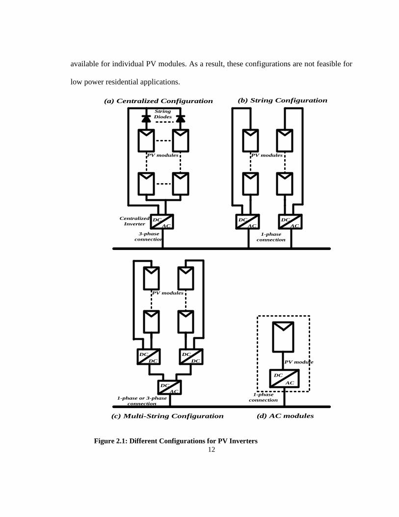
12
available for individual PV modules. As a result, these configurations are not feasible for
low power residential applications.
DC
AC
String
Diodes
PV modules
3-phase
connection
Centralized
InverterDC
AC
PV modules
1-phase
connection
DC
AC
DC
DC
PV modules
1-phase or 3-phase
connection
DC
DC
DC
AC
DC
AC
PV module
1-phase
connection
(a) Centralized Configuration (b) String Configuration
(c) Multi-String Configuration (d) AC modules
Figure 2.1: Different Configurations for PV Inverters

13
2.1.3 AC Modules / Micro-inverters
In order to overcome the drawbacks associated with the centralized approach, the
concept of the AC modules has been introduced in the recent past. The need of long dc
wires could be overcome by using grid tied DC-AC inverters for each PV panel as shown
in Figure 2.1(d). The AC module is the integration of the PV panel and a small grid-tied
inverter in one electrical device to harvest the energy [15]. In this modular approach, the
AC module performs maximum power point tracking (MPPT) of the PV panel, voltage
amplification, galvanic isolation, and injection of the high quality AC current to the
utility grid. The individual MPPT for each module provides an efficient scheme to
overcome the detrimental effects of partial shading and the mismatch losses [15]. In
addition, the modular structure provides a very easy and practical solution for expansion
of the power generation system. The compact nature, high efficiency and scalability make
micro inverters a good candidate for low power (below 500W) residential applications.
[14][15][16]
Despite the numerous advantages of the modular approach, there are a few
complications that should be considered for the design of a micro-inverter.
The size and number of components used in the design of micro inverter is a
major concern as the inverter is installed at the back of each PV module. In order
to achieve individual MPP tracking, a large electrolytic capacitor is required for
decoupling. Hence the limitation of space on the back of the modules is usually a
major concern in this regard.

14
The electrolytic capacitor reduces the overall life span of the micro inverter. The
design of the inverter tends to become complicated on trying to replace the
electrolytic capacitor as additional circuits are needed to achieve power
decoupling.
In case of a fault in the inverter, replacement of the inverter is a difficult and
costly proposition. Even though the installation cost is lower as compared to other
configurations, the maintenance cost of micro-inverters is quite high. [14].
2.2 Review of Single Phase Micro-inverter Topologies
The major tasks performed by a grid connected micro-inverter include extraction
of DC power from the panel, MPPT, voltage amplification to achieve grid voltage and
injection of the sinusoidal current to the grid. It is possible to categorize the inverter
topologies based on the schemes used for distribution of these tasks. One of the common
classifications is based on the number of stages of power processing. The DC to AC
power conversion within the PV module could be carried out either in a single stage or
multiple stages. The block diagram for both multi-stage and single-stage inverter
topologies are shown in Figure 2.2. The subsequent section takes a look at the features of
various existing topologies commonly used for micro-inverters.

15
PV
DC
ACgrid PV
DC
ACgrid
DC
DC
a) Multi-stage Inverter b) Single-stage Inverter
Figure 2.2: Types of Inverter based on processing stages
2.2.1 Multi-Stage Micro-inverters
In multi-stage topologies, the tasks performed by the grid connected system are
distributed into two stages. Extraction of the maximum power from the PV panel and
voltage amplification is usually carried out by a DC-DC converter in the first stage. The
second stage is an inverter, which injects high quality current to the utility grid. The
output of the converter in the first stage could be either a pure DC voltage or a rectified
AC current. In case of a pure dc output voltage, DC-DC converter has to only handle the
nominal power and inverter in the second stage controls the grid current by means of
pulse width modulation. While the DC–DC converter has to handle twice the nominal
power in case of a rectified AC current at the output of the first stage and the inverter
stage switches at line frequency to unfold the rectified current.
The multi-stage topology has a boost type DC-DC converter section which
provides the necessary voltage amplification at the DC link. The increased voltage at the
DC link helps in reduction of the capacitance value at the link. A lower capacitance
eliminates the use of electrolytic capacitors thereby increasing the life span of the micro-

16
inverters. A two-stage micro inverter with a simple power stage and control scheme was
proposed in [17] as shown in Figure 2.3. The topology consists of a DC-DC flyback
converter as the first stage for voltage amplification and galvanic isolation. The second
stage has a full bridge inverter that carries out the AC current injection to the grid.
Though, it provided a robust operation, it suffers from high switching losses as all the
power MOSFET’s are hard switched in this topology.
Idc
Sm
C1
D1
Lf
Utility
Grid
S1
S2
S3
S4
iSm
CdcACCf
PV
Vdc
T
Figure 2.3: Two Stage PV system with flyback converter to boost DC voltage
Since the size of the inverter in AC modules is a major criteria, it is important
achieve high efficiency with minimum components. In [18], a boost converter operating
under Discontinuous Conduction Mode (DCM) is used to generate a high stable DC
voltage. The boost converter uses Pulse Train control algorithm which provides a fast
dynamic response and a robust operation [19]. A high frequency flyback inverter with
peak current mode control is employed for high quality AC current generation. The
flyback inverter configuration is simple and uses fewer semiconductor switches as shown
in Figure 2.4. Although this configuration reduces the overall cost of the system, there is

17
a significant loss associated with this topology as soft switching is not achieved in most
of the switches.
M2
D3 Lf
Utility
Grid
M3
M4
Cin
ACCf
PV M1D4
D2
D1
Lo
Vc2 C2
Figure 2.4: Flyback Inverter with a DC-DC boost converter for voltage amplification
In order to increase the efficiency of the multi-stage micro-inverters, different
schemes needs to be employed to achieve soft switching in either DC-DC or DC-AC
conversion stages or both stages of the micro-inverter. A two stage micro-inverter
consisting of a high efficiency step-up DC-DC converter and a full bridge DC-AC
inverter was implemented in [20]. An active clamping flyback converter with a voltage-
doubler rectifier is used in the first stage which reduces the switching losses by
eliminating the reverse-recovery current of the output rectifying diodes. Figure 2.5
shows the two stages of the micro-inverter.

18
Ipv
S1
Cd
LoS1
S2
S3
S4
i1
Cpv ACCoPV
Vpv
Tvgrid
igridDo2
Do1
Llk
Lm
Cr
Ds1
S2
Ds2
id
iCd
Figure 2.5: Active Clamp Flyback Converter with Full-Bridge Inverter
Another approach that is being implemented in a number of multi-stage micro-
inverters, to improve the efficiency, is the use of resonant circuits to achieve ZVS for the
power MOSFET’s [21-23]. An example of the resonant converter for PV application is
the topology in Figure 2.6 which uses a two-inductor boost converter operating under
resonance condition to provide the soft switching of the power MOSFET’s [21]. The
boost converter operates under variable frequency to secure an adjustable output voltage
range while maintaining the resonant switching transitions.
Co
D1
Q1
L1L2
Lr
D2
D3 D4
Q2
C1 C2
R
E
Vo
Figure 2.6: Two-Inductor Boost converter

19
Soft commutation of the switches with the help of Capacitive Idling technique has been
introduced in [24]. This circuit topology is derived from SEPIC converter and a two-
switch flyback inverter such that soft switching is obtained for the active switches as
shown in Figure 2.7. The major disadvantage with the proposed topology is the increase
in conduction losses in the boost MOSFET since it carries both the input current and the
reflected output current. A comparison of some of the existing micro-inverters with a DC
link has been presented in [13][25].
Grid
Sac1
Sac2
Cf
Lf
vgrid
igri
d
i2Dac1
Dac2
L3
L4
D1L2PV
Vdc
Idc
Cdc
L1
iL1
S1
S2
D2iC1
C1
iL2
1:N:N
iL3
iL4
Figure 2.7: Inverter based on capacitive idling technique
Although the two stage configuration is a very straightforward and simple power
conversion technique, it has some essential limitations. The main limitations of the two-
stage converter are the size and the maximum efficiency achievable to interface the PV
panel to the utility grid. Since there are two stages of power conversion, the efficiency is
inherently limited and also power density of the converter is compromised by the two
stages. The other setback of the two-stage configuration is that it is very difficult to

20
realize ZVS for the second stage of the converter. Therefore, usually a low switching
frequency PWM inverter is used to minimize the inevitable switching losses of the
second stage. Operating with low switching frequency requires a bulky and lossy filter to
remove the high frequency component and inject a high quality current to the grid.
2.2.2 Single Stage Micro-inverters
In a single stage micro-inverter, all the tasks are performed by a single DC-AC
inverter. Since there would be power oscillations at twice the grid frequency, the inverter
would have to be designed to handle a peak power equal to twice of the nominal power.
The size of the inverter can be reduced due to lower component count in single stage
inverters as compared to the multi-stage inverters. A micro-inverter having dedicated
converter for voltage amplification and inverter for sine wave grid current generation
results in increased number of components and its overall size. With the recent trend of
miniaturization, compact single stage micro inverters have become the point of interest
[26-28]. Since the single stage inverters do not have the flexibility of reduction of the size
of capacitor size at the dc link, power decoupling needs to be taken care by either a large
electrolytic capacitor at the input terminals or by use of auxiliary circuits [29-32].
A flyback inverter is one of the common topologies considered for PV modules
since it provides a simple circuit configuration to achieve direct conversion of the DC
power to AC power. The flyback topology has proved to provide a reliable and cost
effective topology with reduced number of semiconductor switches [33]. Another
important feature of flyback topology is the provision of isolation due to the use of high

21
frequency transformer. These benefits of a flyback inverter make it a viable solution for
the single stage micro inverters.
The flyback inverter can operate in Continuous Conduction Mode (CCM) or
Discontinuous Conduction Mode (DCM) to process the power. The CCM operation is not
a feasible solution as the inverter tends to act as a load independent voltage source due to
the incomplete discharge of the magnetizing inductance of the transformer [34]. Another
major issue with the CCM operation is the presence of right half plane zero in the output
current to the duty cycle transfer function, which introduces a challenge in controlling the
output current. Charge control was adopted to control the input current waveform instead
of the output current in [35] to operate the inverter in CCM. However, the charge control
scheme may cause sub-harmonic oscillations. It, also, may result in a constant change in
the operating mode of the inverter between CCM and DCM, under certain operating
conditions. As a result, the DCM has been more attractive solution in the past for flyback
inverters even though the voltage and current stress are higher on the power switches.
In [36], the analysis of the conventional flyback inverter has been performed.
Figure 2.8 shows the conventional single stage flyback inverter operating in DCM. The
efficiency of the flyback inverter is fairly low due to the hard switching of the power
MOSFETs in the conventional configuration.

22
PV
Vdc
Cdc
T
Sm
Idc i1
L1
Cm
Grid
Sac1
Sac2
Cf
Lf
vgrid
igridDac1
Dac1
L2
L3
Figure 2.8: Conventional grid connected flyback inverter
In [37], a soft switching scheme is proposed for flyback inverters through actively
switched snubber circuit in parallel to the primary switch. However, adding extra active
and passive components increases the system complexity and offsets the advantage of the
proposed approach. Figure 2.9 shows the additional components used to achieve ZVS.
PV
Vdc
Grid
Cdc
T
Sm
Sac1
Sac2
Cf
Lf
vgrid
Idc i1
igridi2
Dac1
Dac2
Sa
L1 L2
L3
Da
Cm
Cr
Figure 2.9: Flyback Inverter with actively switched snubber for ZVS

23
Active clamp circuits are also commonly used in flyback inverters in order to
achieve soft-switching and clamp the voltage across the switch thereby reducing the
voltage stress on power MOSFETs [38, 39]. Although, the switching losses and the
voltage stress in the primary switch are mitigated with the active clamp approach, the
additional switch used in the clamp circuit is usually hard-switched which results in
additional switching losses especially at high switching frequencies. The above
mentioned topologies use a high frequency center tapped transformer for the unfolding
stage. Figure 2.10 shows a flyback topology which avoids the use of center tapped
transformer thereby improving the magnetic design [40]. It uses two flyback converters,
one for each half of the ac cycle, and bidirectional switches on the secondary side.
S1
S2
S3
S4
Sacp1 Sacp2
grid
PV
Vdc
Cdc
Idc
W2
W1 vgrid
igrid
Figure 2.10: Flyback Inverter with full bridge configuration on primary side
Resonant based flyback inverters are also the other approach to obtain soft
switching for flyback inverters [41, 42]. In [42], a single-stage quasi-resonant flyback
inverter with a Pulse Frequency Modulation (PFM) control scheme has been proposed as

24
shown in the Figure 2.11. The PFM uses a constant on-time and a variable frequency to
control the energy transfer from the input to the output. The resonant capacitor in the
secondary winding helps provide soft switching.
Lres
iLres
Dfly
Sfly
Cres Co
Drec Lo
Utility Grid
iSfly
iCres
iDrec iLo
VDC
S1
S2
S3
S4
+
-
Figure 2.11: Single-stage Flyback with PFM control
Despite the benefits of achieving ZVS in DCM operation of flyback inverters,
there is still a limit on the transferable power due to the inevitable dead-time required for
the complete discharge of the transformer magnetizing energy in each switching cycle. In
order to increase the limit of power transfer capability, the boundary conduction mode
(BCM) has been proposed, which eliminates the dead-time [34, 43]. In [34] the features
of a flyback inverter in constant frequency DCM and a variable frequency BCM have
comprehensively been analyzed. The control scheme used for BCM operation is,
however, more complicated than the conventional DCM operation due to the addition of
secondary current sensor. Since higher power can be achieved in BCM operation, a dual
switching strategy was proposed in [43], where the mode of operation changes between
the BCM and DCM according to the input conditions. Even with an increase in the power

25
level, the switching losses contribute towards reduced efficiency levels in these
references.
2.3 Concept of Proposed Topology
In order to overcome the aforementioned problems, a novel Zero Voltage
Switching (ZVS) approach in a grid connected single-stage flyback inverter without
using any additional auxiliary circuits. The flyback inverter is operated in modified BCM
in order to maximize the transferable output power. The proposed modified BCM
operation allows the charging of the transformer magnetizing inductance in the reverse
direction of power flow to provide reactive current for soft-switching. The combination
of a switch and diode in the conventional flyback inverters in the secondary is replaced
by a bi-directional switch to permit the current to conduct from the grid-side to the
primary-side. Thus, the presence of negative current during the turn ON of primary
switch results in a soft-switched turn ON of the primary MOSFET. Further, the
secondary MOSFET that replaces the diode is turned ON under ZVS thereby improving
the overall efficiency of the inverter. The proposed concept requires an efficient control
of the amount of reactive current to attain high quality current injection to the utility grid.
Hence, a variable frequency approach for the switching of the MOSFETs based on the
amount of reactive current is introduced in the proposed scheme. The working principle,
detailed analysis and the development of the control scheme of the inverter form the gist
of the thesis.

26
2.4 Summary
In this chapter the different configurations for interfacing of the PV panels to the
utility grid were reviewed. It was observed that the benefits of AC module concept and
their utility made it an ideal candidate for low power PV systems. Thus, a brief review of
the features of existing topologies for the AC modules was conducted. A look into the
features of these topology showed the various issues related to previously proposed
inverters such as
Lower efficiency due to hard-switching of power MOSFET’s
Presence of auxiliary circuits to achieve soft-switching.
Larger component count for two stage inverters
Limitation in power transfer for DCM operation of flyback based topologies
The review especially concentrates on the flyback topologies because of its reliability
and the simplicity due to reduced number switches. A brief idea of the proposed flyback
inverter topology is presented in this chapter.

27
Chapter 3
Proposed Micro-Inverter: Main Circuit Topology
The review of the present scenario of PV generation for residential applications
gives an insight into the drawbacks associated with the existing topologies. It provides an
understanding of the factors that need to be considered while designing the micro-
inverter. On the basis of the review, a single-stage inverter is proposed, which offers soft-
switching for the power MOSFETs, leading to a very efficient and compact solution to
interface the PV panel to the utility grid. This chapter concentrates on the detailed
working of the main circuit topology.
3.1 Principle of Operation
Figure 3.1 shows the circuit diagram of the proposed topology based on a single
stage flyback inverter. The topology consists of a center tapped flyback transformer, a
primary switch, input decoupling capacitor, bidirectional switches on the secondary and
the output filter. The proposed circuit is similar to a conventional flyback inverter with
bi-directional switches in the transformer secondary providing the unfolding of the grid
current. Proper switching of the bi-directional switches on the secondary helps in
achieving soft commutation for most of the switches without the need of any additional
circuitry.

28
PV
Vdc
Grid
Cdc
Np : Ns
Sm
Sacp1 Sacp2
Sacn1 Sacn2
Cf
Lf
vgrid
Idc iSm
iseciSacp igrid
Csn
Figure 3.1: Circuit configuration of the proposed flyback inverter
The primary switch Sm is triggered to charge up the magnetizing inductance up to
the required reference as is the case with a conventional flyback converter. The energy
stored in the magnetizing winding is transferred to the grid by turning ON either the
secondary switch Sacp1 during the positive or Sacn1 during the negative half cycle
respectively. On completion of the power transfer to the grid, the magnetizing inductance
of the transformer is allowed to charge in the opposite direction with the help of the
bidirectional switches on the secondary of the transformer. Figure 3.2 shows the detailed
modes of operation of the proposed circuit in one switching cycle. Since the flyback
inverter operates under modified BCM, the switching frequency is variable. A switching
cycle is divided into six modes of operation. Since the switching frequency of the inverter
is significantly higher than the grid frequency, the quantities varying with respect to the
grid frequency such as the grid voltage, grid current, duty cycle and reference current are
considered constant during one switching cycle.
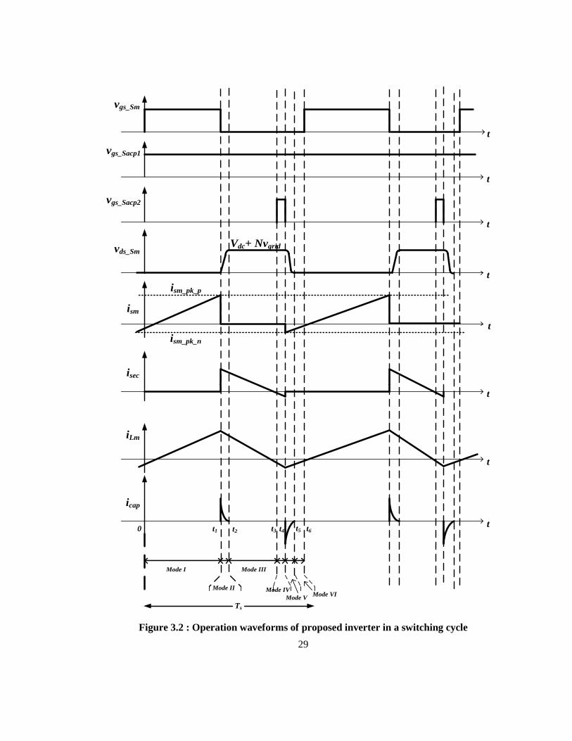
29
vgs_Sm
t
vgs_Sacp1
vgs_Sacp2
t
t
vds_Sm
ism
isec
iLm
icap
Vdc+ Nvgrid
ism_pk_p
ism_pk_n
t
t
t
t
Mode I
Mode II
Mode III
Mode IV
Mode VMode VI
0 t1 t2 t3 t4 t5 t6
Ts
t
Figure 3.2 : Operation waveforms of proposed inverter in a switching cycle

30
Mode I (Interval 0 < t < t1)
The primary switch Sm is turned ON while all the other switches remain OFF. Figure 3.3
shows the components that are active during this interval. The input PV voltage is applied
across the magnetizing inductance Lm of the transformer primary. Hence, the primary
current increases with a slope dependent on the voltage applied across the inductor. The
primary current can be expressed as:
_ _( ) dcsm sm pk n
m
Vi t t i
L
(3.1)
When the current reaches the peak value ism_pk_p at t = t1, primary switch is turned
OFF. The peak value of the switch current is given by the expression:
1_ _ _ _dc
ssm pk p sm pk n
m
Vi d T i
L (3.2)
where, d1 is the duty cycle
ton= d1Ts is the duration for which the primary switch is ON.
The value of ism_pk_p depends on the instantaneous value of the ac output power. The
average value of the input current can be expressed by integrating the primary current
over the switching cycle.
2 2_ _ _ _
2avg
msm pk p sm pk n
Sdc
Li i i
V T (3.3)
One of the secondary bidirectional switches (Sacp1 or Sacn1) depending on the ac cycle) can
be turned ON during this interval as the transformers are connected similar to a flyback
operation.

31
PV
Vdc
Grid
Cdc
Np : Ns
Sm
Sacp1 Sacp2
Sacn1 Sacn2
Cf
Lf
vgrid
Idc iSm
iseciSacp igrid
Csn
Figure 3.3: Equivalent Circuit for Mode I
Mode II (Interval t1< t < t2)
Switch Sm is turned OFF at the beginning of the interval while the secondary switch
Sacp1is ON as shown in Figure 3.4 . The drain-source voltage across switch Sm starts to
rise slowly as the capacitor Csn across the switch starts charging. The polarity of the
transformer is such that the secondary current does not flow even though the secondary
switch Sacp1 remains ON. This mode comes to an end when the capacitor has charged to
its maximum value of Vdc + Nvgrid. This transition from the ON state to OFF state of
switch Sm occurs within a very short interval of time.

32
PV
Vdc
Grid
Cdc
Np : Ns
Sm
Sacp1 Sacp2
Sacn1 Sacn2
Cf
Lf
vgrid
Idc iSm
iseciSacp igrid
Csn
Cap Charging
Figure 3.4: Equivalent Circuit for Mode II
Mode III (Interval t2< t < t3)
During this interval, either the secondary switch Sacp1 or Sacn1depending on the
positive or negative half cycle of the grid voltage is ON. Hence, the energy stored in the
magnetizing inductance of the transformer is released to the grid. Figure 3.5 highlights
the active switch Sacp1 and the anti-parallel diode of switch Sacp2 during this interval.
PV
Vdc
Grid
Cdc
Np : Ns
Sm
Sacp1 Sacp2
Sacn1 Sacn2
Cf
Lf
vgrid
Idc iSm
iseciSacp igrid
Csn
Figure 3.5: Equivalent Circuit for Mode III (positive half cycle)

33
Mode IV (Interval t3< t < t4)
At the beginning of this mode of operation, the anti-parallel diode of the switches
Sacp2 or Sacn2 are conducting depending on the polarity of grid voltage. As the current in
the magnetizing winding tends to zero, either Sacp2 or Sacn2 is switched ON with zero
voltage depending on the sign of grid voltage. The secondary current isec would continue
to flow until it reaches zero. Since the bidirectional switches are ON, the current in the
secondary side changes direction and starts charging the magnetizing inductance in the
opposite direction. At the instant when isec equals the reference value, the secondary
switches are turned OFF. Figure 3.6 shows that both the switches Sacp1 and Sacp2 are ON
during this interval allowing the secondary current to reverse its direction. Since the
voltage observed across the magnetizing inductance of the transformer remains identical
during the modes III and IV, expressions for current and voltage can be considered as the
same for the two intervals.
PV
Vdc
Grid
Cdc
Np : Ns
Sm
Sacp1 Sacp2
Sacn1 Sacn2
Cf
Lf
vgrid
Idc iSm
iseciSacp igrid
Csn
Figure 3.6: Equivalent Circuit for Mode IV (positive half cycle)

34
Thus, in the interval t1< t < t4, the absolute value of secondary current can be
expressed as
_ _
sec 12| | ( )
grid sm pk p
m
v ii t t
N L N
(3.4)
N denotes the turn’s ratio of the transformer (Ns/Np). At the instant t = t4, the secondary
current equals the ism_pk_n/N. Substituting the value of secondary current in (3.4), the
expression for the duty cycle for the interval when the secondary switches are ON can be
obtained as
_ _ _ _
4 1 2 3
( )( )
msm pk p sm pk n
S
grid
i i NLt t d d T
v
(3.5)
where, d2 and d3 are the duty cycle for intervals III and IV respectively.
Mode V (Interval t4< t < t5)
This mode begins when the bidirectional switches on the secondary are turned
OFF as shown in Figure 3.7. Thus all the switches are in OFF state during the interval. As
the magnetizing inductance Lm was charged in reverse direction in the previous interval,
current iLm flows in the direction so as to transfer the energy stored in Lm to the input
capacitor. The voltage across the switch Sm starts decreasing slowly as the capacitor
across the switch starts discharging. This mode comes to an end with the complete
discharge of the capacitor across the switch.

35
PV
Vdc
Grid
Cdc
Np : Ns
Sm
Sacp1 Sacp2
Sacn1 Sacn2
Cf
Lf
vgrid
Idc iSm
iseciSacp igrid
Csn
Cap
Discharging
Figure 3.7: Equivalent Circuit for Mode V
Mode VI (Interval t5< t < t6)
As the capacitor is completely discharged, the drain-source voltage of the primary
switch Sm nearly equals zero. It causes the anti-parallel diode of the switch to conduct as
shown in Figure 3.8. Hence the magnetizing current iLm continue to increase from its
negative value. Since the drain source voltage has been forced to zero, the primary switch
can be turned on with ZVS during this interval.
PV
Vdc
Grid
Cdc
Np : Ns
Sm
Sacp1 Sacp2
Sacn1 Sacn2
Cf
Lf
vgrid
Idc iSm
iseciSacp igrid
Csn
Figure 3.8: Equivalent Circuit for Mode VI

36
It can be observed that Modes II, V and VI occur during the transition between the
switching of the different switches in the circuit. As a result, the time intervals of these
modes are quite small as compared to the Modes I, III and IV. Also, it is clear from the
circuit operation that the duty cycle is basically split into two parts such that
2 3 1(1 )d d d (3.6)
Hence expression (3.5) can be written as
_ _ _ _
1
( )(1 )
msm pk p sm pk n
S
grid
i i NLd T
v
(3.7)
The high frequency component present in the secondary current is filtered by an L-C
output filter such that the average value of the secondary current during the switching
interval TS is obtained by integrating the |isec| over the period.
_ _ _ _
2 2_
_
| | ( )2 sm pk p sm pk n
msec avg
s avggrid
Li i i
v T (3.8)
The above expressions were derived for one switching cycle. In order to have a
holistic view of the operation of the circuit, the waveforms over an AC cycle are shown
in Figure 3.9.

37
iprim_ref(ωt)
isec_ref(ωt)
ωt
ωt
Tac
Iprim_ref_peak
Iprim_ref_peak/N
vgrid(ωt)
ωt
Vgrid_pk
Ts
ism
isec
Isec_ref_peak
Figure 3.9: Waveforms of proposed flyback inverter over an ac cycle
The peak of the magnetizing current is controlled according to the sinusoidal
reference iprim_ref(ωt). Similarly, the peak of the secondary current that charges the
magnetizing winding in opposite direction is controlled according to the sinusoidal
reference isec_ref(ωt).
_ singrid grid pkv V t (3.9)
_ singrid grid pki I t (3.10)

38
_ _ _ _ _( ) ( ) sin( )sm pk p prim ref prim ref peaki t i t I t (3.11)
_ _ sec_ sec_ _( ) ( ) sin( )sm pk n ref ref peaki t Ni t I t (3.12)
The polarity of the average secondary current is determined by the switch Sacp (for
positive half cycle) and Sacn (for negative half cycle) for injection of the AC current into
the utility grid. The magnitude of the AC current injected is obtained from the equations
(3.8) - (3.12)and is given as
2 2_ _ sec_ _
_
( )sin( )2
mgrid prim ref peak ref peak
sgrid pk
Li I I t
V T (3.13)
3.2 Design of Circuit Parameters
The magnetizing current of the transformer for BCM operation is shown in Figure
3.10. The ON time of the primary switch is variable while the OFF time remains constant
during a switching cycle. The switching period for the flyback inverter can be expressed
as
( ) ( ) ( )s on offT t t t t t (3.14)
As the peak of the magnetizing current needs to follow a sinusoidal waveform, the ON
time of the switch needs to be controlled according to (3.15).
_( ) sinon on pkt t t t (3.15)

39
ton toff
Variable ConstantTs
ωt
iLm
Figure 3.10 : Transformer magnetizing current for BCM operation
Where, ton_pk is maximum duration for which the primary switch is turned ON in
the AC cycle. It occurs at ωt = π/2when the maximum power needs to be transferred to
the output. The ON time and OFF time can be expressed in terms of the circuit
parameters with the help of equations (3.2) and (3.7).
_ _ _ _( ) ( ) ( ) mon sm pk p sm pk n
dc
Lt t i t i t
V (3.16)
_ _ _ _( ) ( )( )
moff sm pk p sm pk n
grid
NLt i t i t
v t
(3.17)
It can be seen from the equations(3.15) , (3.16) and (3.17) that the OFF time is a constant
and can be expressed as
_
_
dcoff on pk
grid pk
NVt t
V (3.18)

40
The average switching frequency over the ac cycle is obtained to facilitate the designing
of the circuit parameters. It is defined as
_
_
0
1 1
1( )
s avg
s avgs
fT
T d
_
_
1
2 dcon pk
grid pk
NVt
V
(3.19)
where, θ = ωt
3.2.1 Design of Transformers Turn’s Ratio
The selection of the transformer turn’s ratio is the most important aspect in the
magnetic design of the transformer. The selection of the turn’s ratio depends on the
maximum duty cycle of the switch. The duty cycle can be expressed in terms of the turns
ratio, input and output voltage by comparing equations (3.2) and (3.7).
1
( )( )
( )
grid
grid dc
vd
v NV
(3.20)
The plot of instantaneous value of duty cycle over the AC cycle for different
values of transformer turns ratio is shown in Figure 3.11. It can be observed from the plot
that the peak value of duty cycle over the AC cycle is reduced with the increase in turns
ratio. The maximum duty cycle is reached at the instant when maximum power has to be
delivered to the grid. The maximum duty cycle needed to transfer maximum power to
output is increased to around 70-80% for lower turn’s ratio. The variation of maximum

41
duty cycle with the variation in turns ratio for different input voltages is shown in Figure
3.12. Hence, a lower turn’s ratio is not a feasible choice as the higher peak of duty cycle
could result in an incomplete discharge of the magnetizing inductance for a particular
range of operating frequency. In order to design an efficient inverter, a turn’s ratio of 1:5
was chosen for the transformer.
Figure 3.11 : Variation of duty cycle with turns ratio (N) for Vdc= 45V
0 0.5 1 1.5 2 2.5 30
0.1
0.2
0.3
0.4
0.5
0.6
0.7
0.8
0.9
Du
ty C
ycle
(%)
N = 2
N = 3
N = 4
N = 5
N = 6
N = 6
N = 2

42
Figure 3.12: Variation of Duty Cycle with Turns Ratio
3.2.2 Design of Magnetic Inductance for Flyback Transformer
For a flyback topology, the value of magnetic inductance decides the amount of
power that can be transferred to the secondary for a particular operating frequency. In
order to optimum value of magnetic inductance of the transformer for maximum
efficiency, the relationship between the input power and the power transferred to the grid
with respect to the circuit parameters needs to be investigated. Assuming 100%
efficiency and negligible leakage inductances of the transformer, the averaged dc input
power has to be equal to the averaged ac power.
1 2 3 4 5 6 740
50
60
70
80
90
100
Turns Ratio
Du
ty C
ycle
(%
)
Vdc = 35V
Vdc = 45V
Vdc = 75V

43
acdcP P (3.21)
_ _
1
2dc dc grid pk grid pkV I V I (3.22)
The input DC current can be obtained by integrating average primary current over the ac
cycle.
0
1( )avgdcI i d
(3.23)
On integration of the average primary current iavg, derived for the on time of the switch,
the DC current takes the form
_ _ sec_ _
_2
prim ref peak ref peak dcdc
grid pk
I I NVI F
V
(3.24)
where,
2
_ 0
_
1 sin
sin
dc
grid pk dc
grid pk
NVF d
V NV
V
(3.25)
Equation (3.25) can be analytically solved by using the formula
22
_ _ _0
_
1 sin 2
sin
dc dc dc
grid pk grid pk grid pkdc
grid pk
NV NV NVd S
V V VNV
V
(3.26)
where,

44
_ 0
_
1
sin
dc
grid pk dc
grid pk
NV dS
V NV
V
2
1
2_
_
2tan 1
1
dc
grid pkdc
grid pk
NV
VNV
V
(3.27)
Substituting the expression for Idc in (3.22) gives
_ _
_ _ sec_ _
_
grid pk grid pk
prim ref peak ref peak
dcdc
grid pk
V II I
NVV F
V
(3.28)
Hence, the design equation for the magnetizing inductance of the transformer can be
determined from equations (3.15) , (3.16) and (3.28)
_
_ _
sec_ _
_
2
dc on pk
mgrid pk grid pk
ref peak
dcdc
grid pk
V tL
V II
NVV F
V
(3.29)
The secondary reference current isec_ref(ωt) is a small quantity independent of the
input power as its purpose is to provide the necessary current at the primary to achieve
ZVS for the primary switch. Since the circuit operates under a variable switching
frequency, the expression for instantaneous values of frequency can be obtained by
substituting ton_pk in the above expression.
45
_
__ _
sec_ _
_
1
2
2
dcm
dcs avg
grid pkgrid pk grid pk
ref peak
dcdc
grid pk
VL
NVf
VV II
NVV F
V
(3.30)
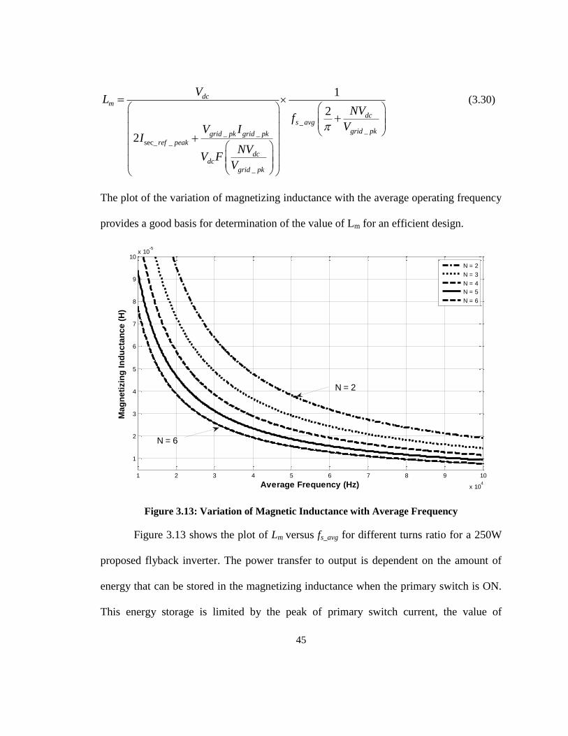
The plot of the variation of magnetizing inductance with the average operating frequency
provides a good basis for determination of the value of Lm for an efficient design.
Figure 3.13: Variation of Magnetic Inductance with Average Frequency
Figure 3.13 shows the plot of Lm versus fs_avg for different turns ratio for a 250W
proposed flyback inverter. The power transfer to output is dependent on the amount of
energy that can be stored in the magnetizing inductance when the primary switch is ON.
This energy storage is limited by the peak of primary switch current, the value of
1 2 3 4 5 6 7 8 9 10
x 104
1
2
3
4
5
6
7
8
9
10x 10
-5
Average Frequency (Hz)
Mag
neti
zin
g In
du
cta
nce (
H)
N = 2
N = 3
N = 4
N = 5
N = 6
N = 6
N = 2

46
magnetizing inductance and the switching frequency. A higher peak current results in a
complex design of the transformer windings. The choice of average operating frequency
and the corresponding value of Lm for a particular turns ratio can be obtained from the
plot in order to keep the peak current within reasonable limits. A magnetizing inductance
of 23µH is used for the transformer.
3.2.3 Flyback Transformer Design
Since the transformer is the most important factor that determines the
performance of a flyback inverter, it is imperative to design a transformer with minimal
losses. In a flyback transformer, the current flows only in the primary side while the core
is charged and in the secondary side only when the core is discharged. The design of the
transformer depends on the mode of operation of the inverter. In the case of either DCM
or BCM operation, high peak-to-peak ripple inductor current at the primary results in
large flux swings. A large variation in flux density leads to high core losses thereby
reducing the efficiency of the transformer. This section explains the procedure followed
for the selection of the core and the various parameters of the flyback transformer.
There are certain design constraints that need to be considered for building an
efficient transformer [44]. The major four are:
Maximum Flux Density: The peak current through the winding (Imax) decides
the maximum flux density (Bmax) at which the transformer can operate. The core
should be selected such that the Bmax is less than the worst case saturation flux
density (Bsat) of the core material. The relation between the flux density and the

47
peak current forms the first design constraint. The constraint is based on the
assumptions that the reluctance of the air gap is much larger than the reluctance
of the core and the leakage inductances are negligible.
max max
0
g
p
lN I B
(3.31)
where, Np is the number of turns in primary
lg is the air gap length
The number of turns and the air gap length should be chosen such that the
maximum flux density is less than Bsat for the known value of Imax.
Inductance: The value of magnetizing inductance required for the rated power
that needs to be obtained, forms the second constraint.
2 0 cm p
g
AL N
l
(3.32)
where, Ac is the cross sectional area of the core
Winding Area: The area of the core available for the windings forms the third
important constraint. The constraint can be expressed as
u p WAK W N A (3.33)
Ku, window utilization factor, is the fraction of the core window area that is
filled with copper.
WA is the window area of the core
AW is the cross sectional area of the conductor

48
The constraint thus states that the area available for winding the
conductors on the core should be greater than the area occupied by the total
number of turns of windings.
Winding Resistance: The relation between winding resistance, the mean-length
per turn (MLT) and the area of the conductor forms the fourth major design
constraint.
( )p
W
N MLTR
A
(3.34)
ρ is resistivity of the conductor material
The total copper loss in the windings is given by:
2 2( ) p tot
Cu
uA
MLT N IP
W K
(3.35)
Itot is the sum of the rms winding currents referred to the primary
The elimination of the unknown quantities from(3.35) and rearranging the
equation gives a relationship between the terms dependent on core geometry and the
specifications. The terms dependent on the core material can be defined as the constant
Kg.
2 2 2
max
2
max
m totg
u Cu
L I IK
B K P
(3.36)
As the value of Kg can be determined from the datasheet of the core manufacturer,
the above equation governs the selection of the core based on the specifications of the

49
inverter circuit. Once the core is selected, various transformer parameters are obtained as
follows:
The maximum flux density that can be handled by the core without getting
saturated is obtained from the manufacturer’s datasheet. In order to calculate the
parameters, an initial value of Bmax lower than the value in the datasheet is
assumed.
Based on the specifications, the number of turns required for the primary
windings is calculated. The fringing flux at near the air gap is not considered in
this case.
4max
max
10mp
c
L IN
B A turns (3.37)
The length of air gap that needs to be provided is determined from expression
(3.38).
2
80.4
10p c
g
m
N Al
L
cm (3.38)
The fringing flux decreases the total reluctance of the magnetic path and hence
increases the inductance by a factor F as compared to the value obtained from
the inductance equation.
21 ln
g
gc
l GF
lA
(3.39)
Where value of G is dependent on the shape and size of the core

50
The effect of the fringing flux is to reduce the number of turns required for
the windings such that the new number of turns is given by
4100.4
g mFp
c
l LN
A F turns (3.40)
As the number of turns decreases due to fringing effect, the value of maximum
flux density would increase as compared to initially assumed value. The new
value of maximum flux density is given by
max 4max
0.410
FpF
g
N IB F
l
Tesla (3.41)
The maximum flux density taking fringing effect into consideration should be
lower than the Bsat of the core.
Table 3.1: Circuit Parameter Values for Proposed Topology
Circuit Parameters Symbols Values
Output Power Pac 250W
DC Input Voltage Vdc 35V-75V
Input Capacitor Cdc 5mF
Grid Voltage Vac 220V
Centre Tapped Flyback Transformer
Turns Ratio Np:Ns 1:5
Core Type EE55
Magnetizing Inductance Lm 23µH
Number of Turns in Primary Np 11
Peak magnetic flux density Bmax 0.23T
Air gap length lg 0.395cms

51
Using the proposed design scheme, a 250W grid connected single stage flyback
inverter is designed for PV applications. The circuit parameters of the proposed flyback
inverter are summarized in Table I.
3.3 Simulation Results
A 250W flyback inverter was designed and simulated in PSIM software with the
component values obtained from the design procedure mentioned in previous sections
and as listed in Table 3.1. The switch current ism, drain source voltage vds and the gating
for primary switch in Figure 3.14 illustrates the zero voltage switching for the primary
switch. It can be seen that during the turn ON, the gating voltage for primary switch is
applied only after vds has become zero. The negative current seen in the Figure 3.14 is
due to the reverse charging of magnetizing inductance of the transformer which aids the
discharge of MOSFET’s output capacitance. A simple capacitive snubber is used in order
to reduce the voltage spikes observed across the primary switch at turn OFF in the
simulations.
52
Figure 3.14: Simulation waveforms of ZVS for primary switch
The bidirectional switches in secondary are also soft-switched at turn ON as
shown in Figure 3.15. It can be observed that the voltage across the secondary switch is
zero during their turn ON. The current isec is shown inverted since it is negative with
respect to the additional switch during the energy transfer to the output. Proper selection
of the snubber capacitance helps in achieving soft switching for most of the switching
cycles within the ac cycle.
Figure 3.15: Simulation Waveforms of ZVS for secondary switch
53
The variation of the primary switch voltage and the switch current over the AC
cycle for an input DC voltage of 45V is shown in Figure 3.16. It can be observed from
the simulation waveforms that the negative portion of the primary current variation is
sinusoidal.
Figure 3.16: Simulation waveform for primary switch voltage and current over ac cycle
A pair of secondary MOSFET’s switch at line frequency while the other pair
switches at the high frequency. The gating of the secondary MOSFETs along with the
switch current for the positive half cycle is shown in Figure 3.17.
Figure 3.17: Secondary switch gating and current waveforms in ac cycle
54
The closed loop output current and the grid voltage waveforms are shown in
Figure 3.18. It can be observed that the grid voltage and the output current are in phase.
Figure 3.18: Output Current and Grid Voltage waveforms
3.4 Experimental Results
On the basis of the foregoing design procedure, a 250W prototype is implemented
to verify the performance of the proposed inverter. In order to implement the controller,
the floating point TMS320F28335 eZdsp was employed. The grid voltage and the output
ac current were sensed and conditioned before inputting to the 12-bit ADC of the
processor. The synchronization of the grid was carried out digitally by extracting the
phase from the grid voltage with the help of grid synchronization algorithms. The phase
extracted from the algorithm aids in determining the reference signals required for the
charging of the magnetizing winding in the reverse direction. Since the knowledge of
transformer secondary current is required to generate the gating pulse for the bidirectional

55
switches, it is sensed with the help of a current transformer. The secondary current
provides the information required to turn on the bidirectional switches. The ePWM
modules in the DSP, generate the gating pulses for the various switches in accordance
with the controller output.
Figure 3.19: ZVS for primary switch
The experimental waveform exhibits soft-switching for both the primary and the
additional secondary switch. Figure 3.19 shows the ZVS of primary switch as the drain-
source voltage is forced to zero before the primary switch is gated. Figure 3.20 shows the
ZVS of secondary switch where the secondary current is inverted with respect to the
bidirectional switches. It can be seen that the drain-source voltage of the secondary
MOSFET is zero, when the gating pulse is applied. As a result, the secondary MOSFET
turns ON under ZVS.
56
Figure 3.20: ZVS for secondary switch
The presence of negative current for the primary switch over the line cycle is
shown in Figure 3.21. The envelope of the negative current follows a sinusoidal
waveform as the negative peak of the primary current is controlled to optimize the
reactive current.
ism
[10 A/div]
igrid
[2 A/div]
Figure 3.21: Grid Current and Primary Switch Current over line cycle
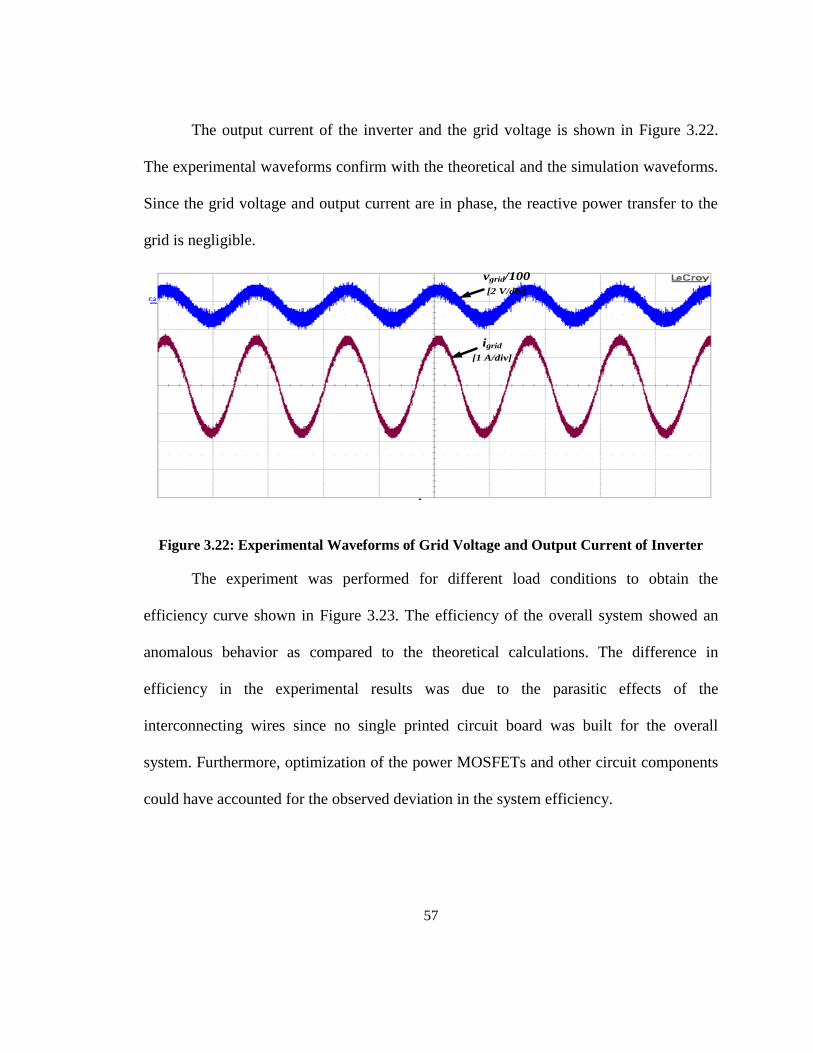
57
The output current of the inverter and the grid voltage is shown in Figure 3.22.
The experimental waveforms confirm with the theoretical and the simulation waveforms.
Since the grid voltage and output current are in phase, the reactive power transfer to the
grid is negligible.
igrid
[1 A/div]
vgrid/100
[2 V/div]
Figure 3.22: Experimental Waveforms of Grid Voltage and Output Current of Inverter
The experiment was performed for different load conditions to obtain the
efficiency curve shown in Figure 3.23. The efficiency of the overall system showed an
anomalous behavior as compared to the theoretical calculations. The difference in
efficiency in the experimental results was due to the parasitic effects of the
interconnecting wires since no single printed circuit board was built for the overall
system. Furthermore, optimization of the power MOSFETs and other circuit components
could have accounted for the observed deviation in the system efficiency.

58
Figure 3.23 : Efficiency Curve of the Proposed Inverter
3.5 Summary
In this chapter, the working of the single stage grid-connected flyback inverter
proposed for PV systems is explained. The detailed analysis of the individual modes of
operation of the inverter is presented along with the theoretical waveforms. The effect of
presence of reactive current in the proposed inverter is explored with the help of the
steady-state expressions. The variation of the circuit parameters with respect to the
critical quantities such as input voltage, output power etc. are studied to obtain optimum
values for the circuit parameters. Since transformer is the crucial parameter in the design
of any flyback inverter, a detailed explanation of selection of the core parameters using
the Kg method for the transformer design are provided. The proposed inverter is
60
65
70
75
80
85
90
95
100
20 30 40 50 60 70 80 90 100
Effi
cie
ncy
(%)
% Load

59
implemented based on the design equations explained in this chapter. Simulation and the
experimental results are provided to confirm the feasibility of the proposed inverter
topology.

60
Chapter 4
Inverter Control and Grid Synchronization
4.1 Introduction
The main objective of the PV inverter is to supply active power to the utility grid.
In order to inject a pure sinusoidal current to the grid, the inverter system should have a
feedback loop that causes the output current to follow a sinusoidal reference current. The
feedback system should be designed such that the grid current is accurately regulated and
remains insensitive to disturbances in the input or the grid voltage. Further, the closed
loop system should be stable for the entire operating range.
A dynamic model of the inverter system is required to design the feedback control
for the system. Averaged switch modeling approach is a common technique used to
obtain the large signal model of a converter. The idea in this approach is to take the
average of the converter waveform to effectively predict the low-frequency behavior of
the system while neglecting the high-frequency switching harmonics [44-47]. The switch
network is replaced by basic circuit elements such as dependent or independent voltage
or current source, loss-free resistor or power source based on the averaged terminal
quantities [44, 48, 49]. The resulting equivalent circuit provides the time invariant
averaged switch model of the converter. The small signal model for the inverter is
derived by linearization of the large-signal averaged equivalent circuits. Generally, the

61
control-to-output transfer function obtained by solving the small signal equivalent circuit
of conventional flyback topology has two poles. Moreover, the flyback topology is a non-
minimum phase system due to the presence of right half plane zero in the control-to-
output transfer function caused by the supply of energy during off-period of primary
switch [44]. The inductor dynamics at low frequencies are insignificant since the pole due
to magnetizing inductance of the transformer usually occurs at a frequency closer to the
switching frequency. Thus the effect of magnetizing inductance is usually neglected to
obtain a single pole transfer function for flyback converters.
The conventional averaging methods for dynamical characterization of the power
converters were for fixed-frequency operation. In case of BCM mode of operation of
flyback converters, it would not be possible to use conventional averaging methods due
to variable frequency switching of the power MOSFETs [50]. In [46], the small signal
modeling of a variable frequency flyback topology operating in BCM is derived by using
a modified circuit averaging technique. Though, this model predicted the presence of
right half plane zero, it only gave a first order control-to-output transfer function.
Therefore, the predicted phase behavior of this model was found to be inaccurate at high
frequencies.
In this chapter, the effect of the variable frequency operation on the dynamics of
the proposed flyback topology is studied. The small signal modeling is based on the
modified state-space averaging technique introduced in [51] where the effect of varying
on-time constraints derived from the inductor current waveform is considered. The

62
presence of the negative current for the primary switch in the modified BCM operation
complicates the modeling of the topology. Hence, the effect of the negative current in
taken into consideration while finding the small signal model of the proposed topology.
The effect of magnetizing inductance is considered while obtaining the transfer functions
as it provides a better understanding of the dynamics of the whole system. Since the
output current needs to follow the sinusoidal reference current, the effect of the output
filter is observed while designing the feedback control. The control-to-output transfer
function determined by taking into account the above mentioned criteria helps design a
suitable compensator for a robust and stable control system. A step by step modeling of
the proposed inverter is provided in the subsequent sections of this chapter. The grid
synchronization scheme used for generating the sinusoidal current reference in phase
with the grid voltage is presented in the latter half of the chapter.
4.2 Modeling of the Proposed Flyback Inverter
4.2.1 Modeling Principles for Direct On-Time Control
During a particular switching cycle, the grid side AC quantities are constant as the
switching frequency is significantly higher than grid frequency. Hence, for a switching
cycle, the circuit operation of a flyback inverter is equivalent to a DC-DC flyback
converter. Since the state-space averaging is based on the averaging of the circuit
waveforms over a switching cycle, the steps followed for modeling of the proposed
flyback inverter is similar to a DC-DC flyback converter operating under BCM. The

63
major change in the modeling process is the effect of the negative current in the
magnetizing inductance on the switch current and voltage waveforms. Since a flyback
converter is a transformer-isolated version of a buck-boost converter, modeling of a
buck-boost converter with all the primary-side parameters of a flyback converter
reflected to the secondary would yield the same results [44]. Figure 4.1 shows the
equivalent flyback converter where the input parameters being the reflected quantities.
This circuit represents the operation of the proposed inverter for a particular switching
cycle.
Sm Sacp1 Sacp2
Cfvo
isec io
vin
iin
vL
+
_ vc
+
_
+
_
iL
LiC
Rac
Figure 4.1: Equivalent flyback converter with parameters reflected to secondary
in dcv NV (4.1)
2
mL N L (4.2)
The solution of the system dynamics is obtained by using time-varying averaged
values of inductor current ⟨ ⟩ and capacitor voltage ⟨ ⟩ as the state variables, the input

64
voltage ⟨ ⟩ and output current sink ⟨ ⟩ as input variables, and the output voltage ⟨ ⟩
and input current ⟨ ⟩ as the output variables. In case of a fixed frequency operation, the
duty cycle is usually considered as the fundamental control variable. A constant time
period results in equivalent dynamic properties of both duty cycle and the on-time of the
primary switch. However, under variable frequency operation, on-time ton has to be used
as the control variable because of the different dynamical properties of duty ratio and on-
time [51].
A peak current mode (PCM) control is implemented for the proposed inverter
scheme. The control current for the PCM is the peak of inductor current (ipk). In order to
obtain the state-space equations for PCM, the relation between the on-time and peak
inductor current is calculated. The inductor current waveform, shown in Figure 4.2, gives
the relation between on-time and cycle time constraints for the variable frequency
operation. In each switching cycle, the inductor current rises from its negative peak inpk
until it reaches a peak current equal to ipk..
s on offt t t (4.3)
( )
2
pk npk
L
i ii
(4.4)
2 L
S on
C
L it t
v (4.5)
1
2
onpk L
m ti i (4.6)

65
1
2
onnpk L
m ti i (4.7)
The relation between the on-time and the inductor peak currents needed for PCM can be
obtained from the above expressions.
2 pk L
on
in
L i it
v
(4.8)
2 L npk
on
in
L i it
v
(4.9)
tinpk
ipk
m1 = vin /L-m2 = vc /L
iL(t)
<iL>
ton toff
ts0
Figure 4.2 : Magnetizing Inductor current waveform in modified BCM
In this approach of modeling, the time-varying averaged state variables and output
variables are represented in terms of the circuit parameters. The derivative of the
averaged inductor current is given by

66
1 2
offL on
s s
td i tm m
dt t t (4.10)
Substituting the value of the slopes m1 and m2for the corresponding sub-intervals,
expression (4.10) can be expressed in terms of the state and output variables.
on in CL C
s
t v vd i v
dt t L L
(4.11)
The derivative of the capacitor voltage is approximated based on the average charge
delivered to the capacitor and removed from it in each switching cycle.
1 LC on C o
S f ac f f
idv t v i
dt t C R C C
(4.12)
The average output voltage equals the capacitor voltage as can be seen from the Figure
4.1.
O Cv v (4.13)
The averaged input current for the converter is the average on-time inductor current.
onin L
S
ti i
t (4.14)
The equations (4.11) - (4.14) form the non-linear state and output equations. In order to
find the small signal model, these equations are linearized by using the partial derivatives
[44]. To find the partial derivatives for the time-varying averaged quantities, each
equation is differentiated with respect to the variables individually, keeping the other

67
variables constant. The small signal expression using partial derivative of a function
f(x,y.z) is defined as:
^ ^ ^ ^( , , ) ( , , ) ( , , )
, ,x X z Zy Y
f x Y Z f X y Z f X Y zf x y z x y z
x y z
(4.15)
Hence, the small signal expressions for the different time-varying averaged quantities
using partial derivatives are given by
^
' ^ ^ ^ ^in O in OL
C in on S
S S
V V D V Vd i D Dv v t t
dt L L LT LT
(4.16)
^' ^ ^ ^ ^1C L L
L on O S
S f f S f
d v D I DIi t i t
dt L T C C T C (4.17)
^ ^
C Ov v (4.18)
^ ^ ^ ^L L
in L on S
S S
I DIi D i t t
T T (4.19)
The parameters in uppercase are the steady state values of the state variables (IL,
VC), output voltage (VO), input voltage (Vin) and the duty ratio (D). The steady state value
for the switching period (TS) is given by
'
2 2L LS
in O
LI LIT
DV DV (4.20)
Since the proposed inverter is operating under variable frequency, the small signal
variations of the switching period and the on-time also needs to be considered. The on-

68
time constraint can be considered in terms of both the positive and the negative peak
inductor current.
^^ ^ ^
2
22 LonLS C
O C
LILt i v t
V V (4.21)
^^ ^ ^2
2on
on inLpkin
Ti
Lt i v
V L
(4.22)
^^ ^ ^2
2on
on inL npkin
Ti
Lt i v
V L
(4.23)
The linearized forms of the on-time in (4.22) and (4.23) are with respect to the
positive and negative peak inductor currents in case of the modified BCM operation.
Since both positive and negative peak currents can independently determine the on-time,
it is possible to develop control-to-output transfer functions for both cases individually.
Using these constraints, the dynamics of a peak current mode controlled converter for
both positive and negative peak currents can be obtained as explained in the subsequent
sections.
4.2.2 Transfer Function Derivation
The state space representation of the state variables in terms of the positive peak
current is determined by substituting the expressions (4.21) and (4.22) in the set of linear
differential equations for the state and output variables. The new set of the expressions
are given by

69
^
^ ^2L in inL pk
L L
d i DV DVi i
dt LI LI
(4.24)
^
' ' ' '^ ^ ^ ^ ^1 2 1 1C L LL C in O pk
f ac f O f in f f f
D Dd v DD I DD I DDi v v i i
dt C R C V C V C C C
(4.25)
^ ^
O Cv v (4.26)
' '^ ^ ^ ^ ^
'2 1 L Lin L C in pk
O in
DD I DD Ii D D i v v DD i
V V (4.27)
The set of small signal state space equations can be represented using Matrix
techniques for open loop. In order to obtain the transfer functions, the open loop system
equations can be written in s-domain using the Laplace transforms.
1 1 1( ) ( ) ( ) ( )pksX s A X s BU s E I s (4.28)
1 1 1( ) ( ) ( ) . ( )pkY s C X s DU s P I s (4.29)
The individual terms of the matrices, obtained from the small signal state space equations
(4.24) - (4.27) are
( )( )
( )
L
c
I sX s
V s
( )
( )( )
in
o
I sY s
V s
( )
( )( )
in
O
V sU s
I s
1 ' '
20
1 2 1
in
L
L
f ac f O f
DV
LIA
D D DD I
C R C V C
'
1
0 0
1L
in f
B DD I
V C

70
'
1
2 1
0 1
L
O
DD ID D
C V
'
1
0
0 0
L
in
DD I
D V
1 '
in
L
f
DV
LIE
DD
C
'
10
DDP
The solution of the two simultaneous matrix equations solved using simple matrix
calculus is given by
1 1
1 1 1 1 1 1 1 1( ) ( ) ( )pkY s C sI A B D U s C sI A E P I s
(4.30)
The second term relates the output variable to the control variable. Hence, the control-to-
output transfer function can be determined by calculation of the second matrix.
1
1 1 1 1( )pT s C sI A E P
(4.31)
Since the input variables are set to zero while calculating the control-to-output transfer
function, first term in equation (4.30) becomes zero.
1
2
( )( )
( )
pin
pk
po
GI sI s
GV s
(4.32)
It can be observed that the term Gp2 gives the ratio of output voltage and the positive peak
of inductor current. The calculation of the above matrices yields the required transfer
function for the converter.

71
'
2'
( )2 1
in
O L
p
pk f in L
L O f ac f
Vs
V s LIDDG s
I s C DV DD Is s
LI V C R C
(4.33)
It is evident from the working principle of the proposed inverter that the current
on the secondary side of the transformer is allowed to become negative with the help of
the bidirectional switches. Since the negative current on the secondary side is extracted
from the grid, it is essential to control the amount of reactive current from the grid. With
the change in the atmospheric conditions the amount of current injected to the utility grid
varies. It is important that the magnitude of the negative peak current also vary relative to
the variation in input power. The variation in the negative peak inductor current will act
as a disturbance for the control-to-output transfer function as the average value of
inductor current is dependent on negative peak of inductor current. Hence, the knowledge
of the transfer function for negative peak of inductor current would provide a better
understanding of the system.
The derivation procedure for the transfer function is similar to the method shown
for the positive peak current. The set of small signal state space equations based on the
constraint for negative peak of inductor current in equation (4.23) are given by
^
^L in
npk
L
d i DVi
dt LI (4.34)

72
^' ' ' '^ ^ ^ ^ ^1 1C L L
L C in O npk
f ac f O f in f f f
d v D DD I DD I DDi v v i i
dt C R C V C V C C C
(4.35)
^ ^
O Cv v (4.36)
' '^ ^ ^ ^ ^'L L
in L C in npk
O in
DD I DD Ii D i v v DD i
V V (4.37)
These small signal state space equations can be written in matrix form like the previous
case.
' '2
0 0
1 L
f ac f O f
A D DD I
C R C V C
'
2
0 0
1L
in f
B DD I
V C
'
2
0 1
L
O
DD ID
C V
'
2
0
0 0
L
in
DD I
D V
2 '
in
L
f
DV
LIE
DD
C
'
20
DDP
The matrix equations are solved in order to find the transfer function with respect to the
negative peak of inductor current. The input variables are set to zero to obtain Gn2.
1
2
( )( )
( )
nin
npk
no
GI sI s
GV s
(4.38)

73
'
2'
( )1
in
O L
n
npk f L
O f ac f
Vs
V s LIDDG s
I s C DD Is s
V C R C
(4.39)
A look into the control-to-output transfer functions (4.33) and (4.39) gives an insight into
the behavior of the system. Since, the effect of high frequency pole is considered, this
method exhibit a second-order system behavior. The fact that the flyback converters have
a non-minimum phase is confirmed by the presence of the right half plane zero at
. The effect of the RHP and the high frequency pole is to result in a sharp
decrease in phase of the system. The knowledge of the control-to-output transfer
function provides the foundation for the controller design explained in next section.
4.3 Controller Design of the Proposed Inverter
Figure 4.3shows the block diagram for the control of the output current of the
inverter. It is obvious from the block diagram that a current mode control scheme is used
to regulate the output current from the inverter. The grid voltage is sensed in the outer
loop to generate the sinusoidal current reference for the inner current control loop. Since,
the disturbances in grid voltage may result in amplitude, phase or frequency variation,
PLL block in the outer loop is required to synchronize the inverter output current with the
grid voltage. The PLL block generates the exact phase needed for the generation of
proper sinusoidal grid current reference. The MPPT block extracts the maximum power

74
from the PV panel. Hence, the magnitude of the grid current reference is dependent on
the output of the MPPT block. When the atmospheric conditions are favorable, the grid
current reference would be higher due to increased power available from the PV panel.
MPPT Grid current
Reference
Generation
Output
Current
Controller
InverterOutput
Filter
PLL
Vpv
Ipv+
-
vgrid
igrid
ω
igrid_ref
Figure 4.3: Inverter control block diagram
In order to design the controller for a system, the information of the transfer
function of the uncompensated system is required. The block diagram for the inner
current control loop is shown in Figure 4.4. Equations (4.33) and (4.39) gave the control-
to-output transfer functions only for the plant. The inverter is connected to the grid using
an inductive filter as shown.
The equation governing the dynamic of an inductive filter is given by
grid
f o grid
diL v v
dt (4.40)
where, vo is the inverter output voltage and vgrid is the grid voltage.

75
Controller
H(s)
Plant
Gp(s)
Filter
Gf(s)+-
igrid
igrid_ref
Sensor
ksense
Figure 4.4 : Block diagram for the inner current control loop
The transfer function of the inverter output voltage to the grid current for the inductive
filter is
0
( ) 1( )
( )
grid
f
f
I sG s
V s sL (4.41)
Hence, the loop transfer functions for the open loop or uncompensated system for the
positive and negative peaks of inductor currents are given by equations (4.42) and (4.43)
respectively.
'
_'
( )2 1
in
grid Lsensep uncomp
pk f f in L
L O f ac f
Vs
I s LIk DDG s
I s C L DV DD Is s s
LI V C R C
(4.42)
'
_'
2
( )1
in
grid Lsensen uncomp
npk f f L
O f ac f
Vs
I s LIk DDG s
I s C L DD Is s
V C R C
(4.43)
ksense is the sensor gain.

76
The presence of the RHP zero and the high frequency poles in the control-to-
output transfer function do not adversely affect the magnitude curve of the system but
exhibits a sharp fall in the phase of the uncompensated system at higher frequencies as
shown in Figure 4.5. This sharp fall in the phase causes limitations in the achievable
bandwidth of the closed loop system. It can be observed that the phase of the
uncompensated system drops to around -225 degrees around 2 kHz and continues to fall
rapidly with the increase in frequency. Hence, the compensator should provide a large
phase boost in order to achieve a reasonable phase margin at the gain cross-over
frequency. Larger the bandwidth required, a higher phase boost would be needed.
Since a large phase boost is required for a stable closed loop system, a Type-III
compensator is used for peak current mode control of the compensation of the proposed
inverter. A Type-III compensator can provide a maximum phase boost of 180 degrees
due to the presence of two zeroes in its transfer function. The compensator transfer
function for the peak current mode control is given by
0.00167 1 0.001 1( ) 0.1488
0.00001 1 0.00000667 1
s sH s
s s s
(4.44)
Bode plot for the Type III compensator is also shown in Figure 4.5. Bode plot of the
compensated system for the peak current mode control for the positive peak of the
inductor current is shown in Figure 4.6. A phase margin of 49 degrees is achieved with a
reasonable bandwidth for the closed loop system.
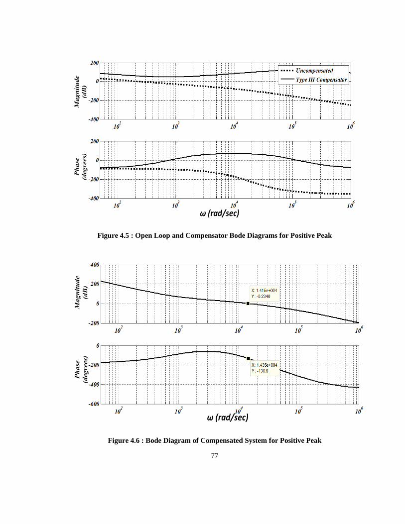
77
Figure 4.5 : Open Loop and Compensator Bode Diagrams for Positive Peak
Figure 4.6 : Bode Diagram of Compensated System for Positive Peak
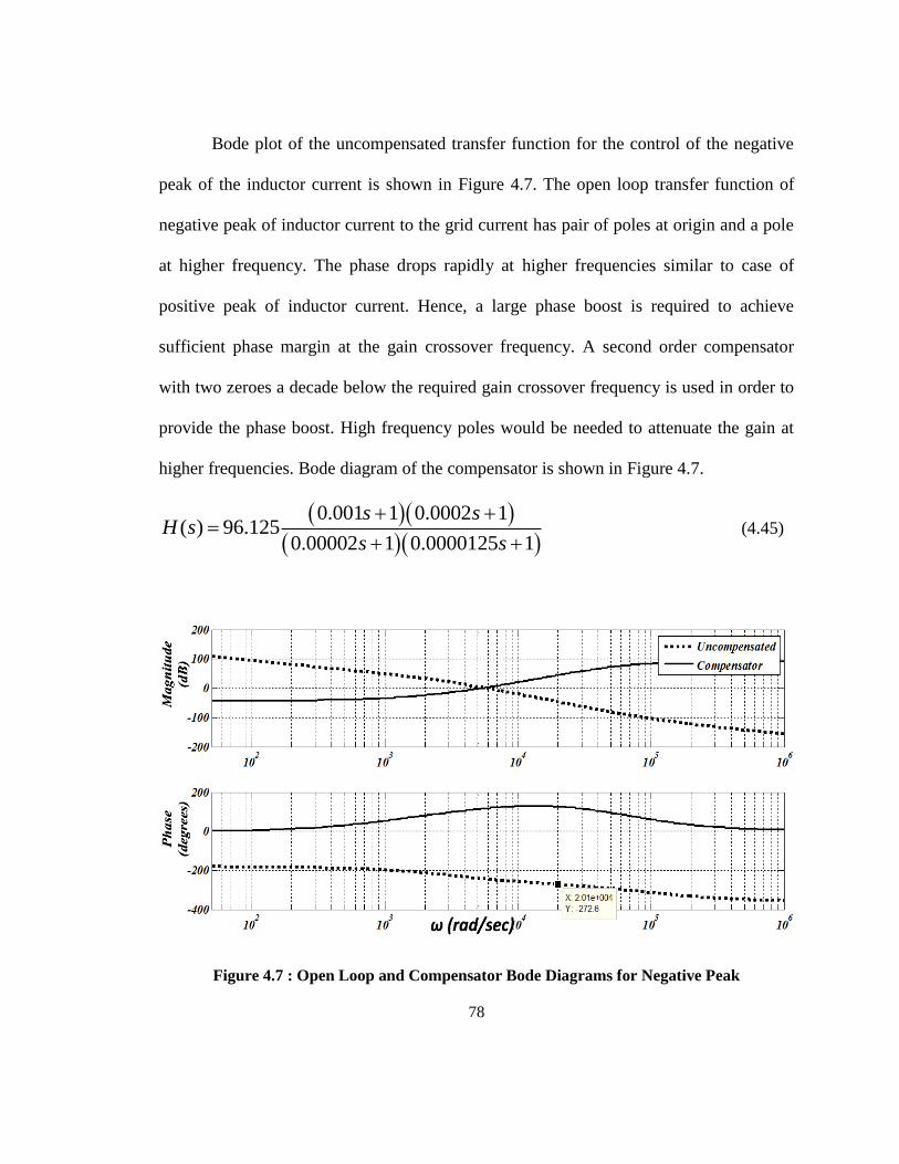
78
Bode plot of the uncompensated transfer function for the control of the negative
peak of the inductor current is shown in Figure 4.7. The open loop transfer function of
negative peak of inductor current to the grid current has pair of poles at origin and a pole
at higher frequency. The phase drops rapidly at higher frequencies similar to case of
positive peak of inductor current. Hence, a large phase boost is required to achieve
sufficient phase margin at the gain crossover frequency. A second order compensator
with two zeroes a decade below the required gain crossover frequency is used in order to
provide the phase boost. High frequency poles would be needed to attenuate the gain at
higher frequencies. Bode diagram of the compensator is shown in Figure 4.7.
0.001 1 0.0002 1( ) 96.125
0.00002 1 0.0000125 1
s sH s
s s
(4.45)
Figure 4.7 : Open Loop and Compensator Bode Diagrams for Negative Peak
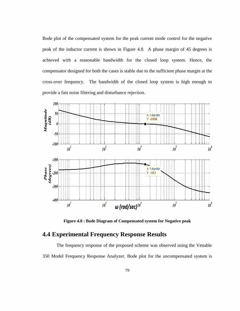
79
Bode plot of the compensated system for the peak current mode control for the negative
peak of the inductor current is shown in Figure 4.8. A phase margin of 45 degrees is
achieved with a reasonable bandwidth for the closed loop system. Hence, the
compensator designed for both the cases is stable due to the sufficient phase margin at the
cross-over frequency. The bandwidth of the closed loop system is high enough to
provide a fast noise filtering and disturbance rejection.
Figure 4.8 : Bode Diagram of Compensated system for Negative peak
4.4 Experimental Frequency Response Results
The frequency response of the proposed scheme was observed using the Venable
350 Model Frequency Response Analyzer. Bode plot for the uncompensated system is
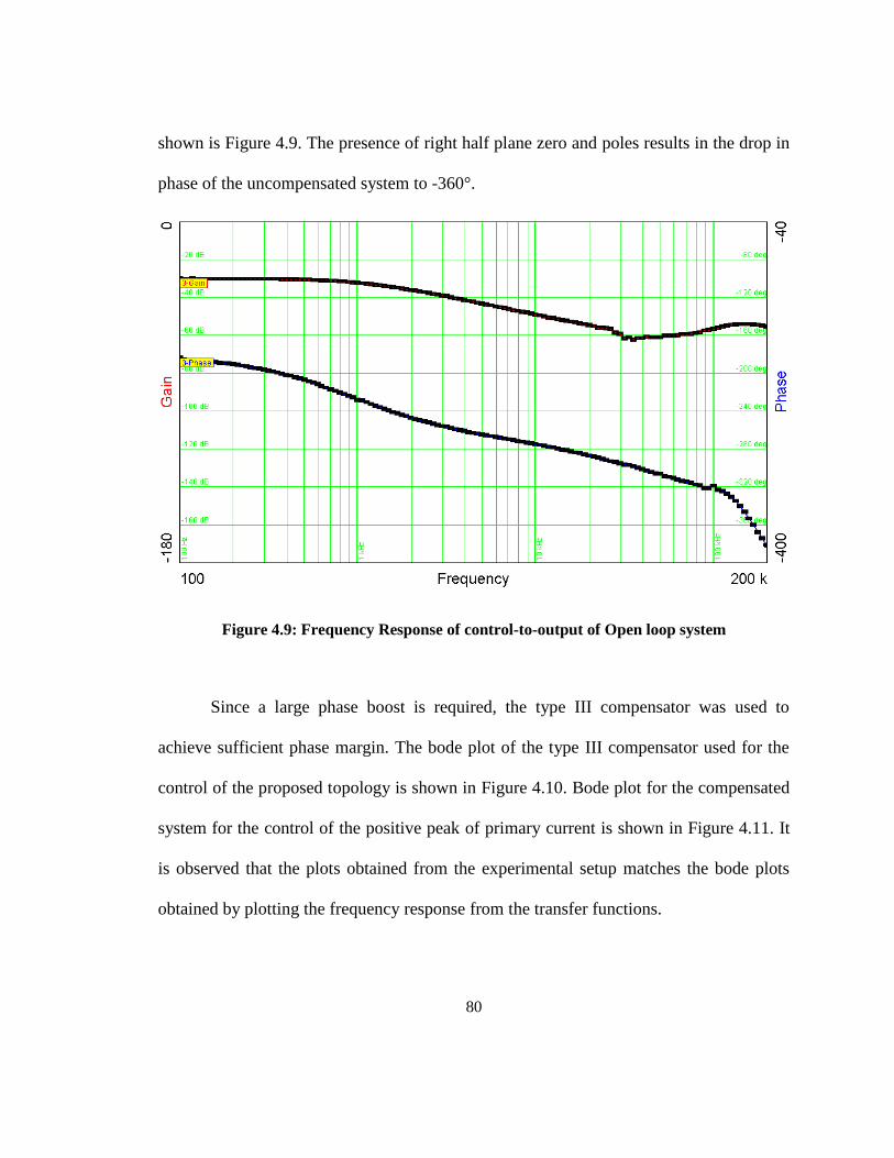
80
shown is Figure 4.9. The presence of right half plane zero and poles results in the drop in
phase of the uncompensated system to -360°.
Figure 4.9: Frequency Response of control-to-output of Open loop system
Since a large phase boost is required, the type III compensator was used to
achieve sufficient phase margin. The bode plot of the type III compensator used for the
control of the proposed topology is shown in Figure 4.10. Bode plot for the compensated
system for the control of the positive peak of primary current is shown in Figure 4.11. It
is observed that the plots obtained from the experimental setup matches the bode plots
obtained by plotting the frequency response from the transfer functions.
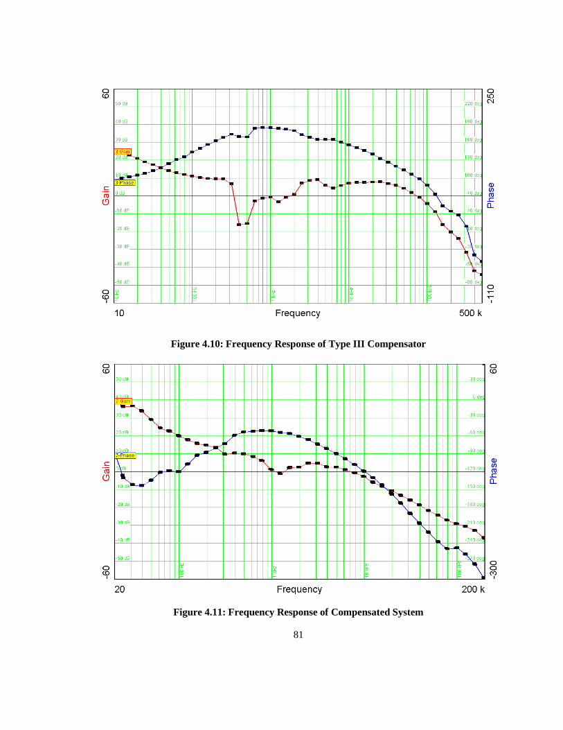
81
Figure 4.10: Frequency Response of Type III Compensator
Figure 4.11: Frequency Response of Compensated System

82
4.5 Grid Synchronization
The presence of the disturbances and harmonics in the grid voltage makes it
unfeasible to use the grid voltage directly as the synchronization signal. Since these
disturbances in the grid should not be reflected on the reference signals for the proper
control of output current, different grid synchronization schemes need to be employed for
grid-connected inverter systems [12]. Phase Locked Loop (PLL) is a nonlinear filter
structure which can extract the phase information from the grid voltage for the grid
synchronization. The task of the PLL is to provide unity power factor operation by
synchronizing the inverter output current and the grid voltage. The PLL structure is
responsible for monitoring and detecting the grid voltage parameters such as phase and
amplitude. The output of the PLL block is used to generate a clean sinusoidal reference,
for output current control loop, independent of the distortions in the utility voltage. [52,
53].
A simple and accurate grid synchronization technique based on the Adaptive
Notch Filtering (ANF) for single phase systems introduced in [54, 55] is implemented for
the proposed flyback inverter in this thesis. The block diagram for the digital form of the
ANF technique using the Bilinear Transformation is shown in Figure 4.12. The input to
the ANF module is the distorted sinusoidal grid voltage. It can be observed from the
block diagram that vα and vβ are the fundamental component and its 90ᵒ
phase shifted
signals of the grid voltage respectively. The ANF scheme is composed of few multipliers,
adders and integrators. The output of one of the integrators of ANF gives the angular

83
frequency ω of the grid voltage. The initial condition for this integrator is set to the
nominal grid frequency. Since the amplitude of the grid voltage can be calculated from vα
and vβ, the sine and cosine functions of the phase angle are easily obtained. The control
parameters for the ANF scheme are ζ and γ. The capability of the algorithm to track the
variations in grid voltage is determined by the convergence factor ζ while the noise
sensitivity of the filter is controlled by the parameter γ.
vgrid(n)+
-
z-1
z-1
z-1
z-1
z-1 z
-1
T/2
T/2
T/2
2ζ
γ
vα(n)
vβ(n)
ω(n)
+ + +
+ +
+
+
+
+
+
+
+
+
+
+
-
ωref
e(n) x1(n)x2(n)
x3(n)
Figure 4.12: Digital Implementation of the ANF technique
The difference equations for implementation of the ANF algorithm are obtained
from the block diagram in Figure 4.12.

84
1 2 ( ) ( )x n e n n (4.46)
12 ( )n nx n x n v
(4.47)
2 21
21
Tx n x nv n v n (4.48)
12
1T
n v n v nv n v n
(4.49)
3 refnx n e v n (4.50)
3 31
21
Tx n x nn n (4.51)
T is the sampling frequency which is chosen as 20 kHz. The simulations waveforms for
the ANF are shown. Figure 4.13 and Figure 4.14 shows the response of the ANF method
when there is a step variation in the frequency of the grid voltage from 60Hz to 65Hz and
65Hz to 60 Hz respectively. It can be observed that the ANF method tracks the variations
in the frequency accurately.
Figure 4.13: Response of ANF where frequency of grid voltage jumps from 60Hz to 65Hz
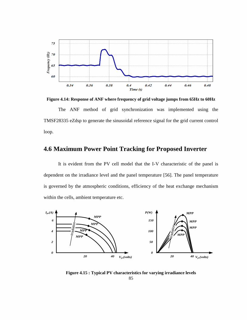
85
Figure 4.14: Response of ANF where frequency of grid voltage jumps from 65Hz to 60Hz
The ANF method of grid synchronization was implemented using the
TMSF28335 eZdsp to generate the sinusoidal reference signal for the grid current control
loop.
4.6 Maximum Power Point Tracking for Proposed Inverter
It is evident from the PV cell model that the I-V characteristic of the panel is
dependent on the irradiance level and the panel temperature [56]. The panel temperature
is governed by the atmospheric conditions, efficiency of the heat exchange mechanism
within the cells, ambient temperature etc.
Ipv(A)
Vpv(volts)
Irra
dia
tion
P(W)
0
2
4
6
20 40
0
50
100
150
20 40 Vpv(volts)
Irra
dia
tion
MPP
MPP
MPP
MPP
MPP
MPP
MPP
MPP
Figure 4.15 : Typical PV characteristics for varying irradiance levels

86
A typical I-V and P-V characteristic of a PV panel for varying irradiation is
shown in Figure 4.15. The points labeled as MPP on the plot are the operating point of
the panel, where it generates the maximum power output for a particular irradiance level.
The unpredictable nature of the atmospheric conditions make it essential to track the
maximum power point continuously to extract maximum power from the PV panel for
the particular set of operating conditions.
Perturb and Observe method is a widely used method to achieve MPPT because
of the ease and the low cost associated with the implementation of the algorithm [57].
The idea of the algorithm is to track the output power of the panel based on a small
perturbation in the PV voltage. If the output power of the PV panel increases when the
voltage is perturbed from its operating point due to the changes in atmospheric
conditions, then we need to continue to increase the PV voltage to reach the MPP. Under
this circumstance, the operating point is on the left of the MPP point in Figure 4.15.
Hence, the perturbation is PV voltage, ∆Vpv, would be positive until it reaches the MPP
point. While a decrease in output power on increase of the PV voltage, signifies a
movement away from the MPP. As a result the direction of voltage perturbation must be
reversed to move closer to the MPP. Since there is a continuous perturbation taking place
in this algorithm, there may be oscillations about the MPP at steady state. In order to keep
the oscillations to minimum, a smaller perturbation step size can be used.

87
The block diagram for the Perturb and Observe method is shown in Figure 4.16.
The PV voltage and input voltages are differentiated to obtain the variation in output
power with respect to the variation in the PV voltage.
d/dt
Vpv
Ipv
d/dt
+ Sgn + Controller+
+
dIpv
dVpv
K
Step Size
pv
dP
dV
Vpv_ref
Output
Figure 4.16: Block Diagram for Perturb and Observe Algorithm
pv
pv pv
pv pv
dIdPI V
dV dV (4.52)
Depending on the sign of the above differential, the reference PV voltage is
adjusted such that the maximum power is extracted from the PV panel. A simple Type II
compensator is used in order to generate the magnitude of the grid current reference for
the inner current loop. The transfer function for the controller is given by
0.2 1( ) 0.667
0.011 1
sH s
s s
(4.53)
The output of the controller is multiplied with the sinusoidal signal that is synchronized
with the grid voltage to obtain the proper grid current reference.

88
4.7 Summary
This chapter dealt with the modeling and control of the proposed inverter for the
implementation of the PV system. The chapter began with an introduction to the
techniques usually employed for the modeling of the inverters. A detailed analysis for the
modeling based on the variable frequency operation of the inverter was presented. With
the help of the small signal state space equations for the dynamics of the system, the
control-to-output transfer function was found. The bode diagram of the open loop transfer
function of the system provided an insight of the uncompensated system. The necessary
phase boost for the uncompensated system was provided with the help of Type III
Compensator in order to achieve a stable closed loop system.
Since the grid synchronization is unavoidable for grid connected inverters, ANF
method is implemented for generation of clean sinusoidal current reference. The digital
implementation of the ANF method with the waveforms is presented. Tracking of the
Maximum Power Point is achieved using the simple Perturb and Observe algorithm.
Hence, this chapter gives the analysis required for the implementation of complete PV
system.

89
Chapter 5
Conclusions
5.1 Summary
With the increase in energy prices and the adverse environmental effects of the
non-renewable energy sources, the interest in improving power generation from solar
energy has grown over the past few decades. In this research, first the role of power
electronics technology in improving the solar power generation in the recent times was
observed. Then the challenges associated with the design of the power converters to
achieve efficient power conversion for PV modules were taken into consideration while
designing the inverter. In addition, an extensive background study on the various existing
inverter topologies for PV module was conducted. It was observed that most of the
existing single-stage flyback based topologies for PV modules used auxiliary circuits to
achieve soft-switching in order to minimize the switching losses in the power MOSFETs.
Thus the main purpose of this thesis was to propose a novel scheme to achieve
ZVS for a single stage grid-connected flyback inverter without the addition of any
auxiliary circuits. The soft-switching of the primary switch was made possible by
allowing a current flow from the grid-side to the transformer which provides the negative
current for soft-switching of primary switch. This concept was implemented by the
inclusion of bidirectional switches on the secondary side of the transformer. The

90
bidirectional switches, not only helped to provide the negative current to achieve ZVS for
primary switch, but were also turned ON under ZVS. Hence, the soft-switching of the
additional secondary MOSFETs meant that the overall efficiency of the inverter was not
affected by inclusion of the extra secondary switches. A detailed analysis and design of
the circuit parameters were presented to achieve an efficient flyback inverter with
minimal possible current and voltage stresses on the switches.
The control system for the proposed inverter was designed with the help of
modified state space averaging technique and the corresponding small signal model of the
inverter. Grid synchronization of the inverters was found to be an important criterion
while designing the complete PV module system. Thus, a grid synchronization technique
based on ANF algorithm was implemented to keep the inverter system tolerant to the
disturbances in the grid voltages. The digital control scheme for the inverter and the ANF
algorithm was executed on a TMS320F28335 processor. The simulation and
experimental results are included in the thesis which verifies the concept for achieving
soft-switching in the proposed inverter topology.
5.2 Contributions
The main contributions of this thesis are summarized below:
1. This thesis proposed a novel scheme of achieving ZVS in a grid-connected single-
stage flyback inverter. Negative current required to turn ON the primary switch
under ZVS, is obtained by allowing the flow of reactive current from the grid-side
to the transformer for a short interval of time. In order to allow the negative

91
current flow, bi-directional switches are included on the secondary side of the
transformer. The combination of a power MOSFET and diode in the conventional
flyback inverters on the grid-side is replaced by a bi-directional switch to permit
the current to conduct from the grid-side to the primary-side. Further, these grid-
side MOSFET that replaced the diode is also turned ON under ZVS thereby
minimizing the switching losses on the secondary side of the transformer as well.
2. The proposed flyback inverter operates in modified BCM in order to maximize
the transferable output power. The modified BCM operation allows the charging
of the transformer magnetizing inductance in the reverse direction of power flow
to provide reactive current for soft-switching. A variable frequency scheme is
implemented over the line cycle for the flyback inverter in order to optimize the
amount of reactive current drawn from the grid-side to achieve ZVS for the entire
operating range.
3. The presence of negative inductor current introduces some subtleties in the
modeling of the proposed scheme. Since there is negative current in the primary
MOSFETs, the effect of the negative peak of the inductor current should be
considered. A modified state space averaging technique is presented to obtain the
accurate small signal model of the system. This precise model can be used to
design the controller for the closed-loop system.
4. A peak current mode control is proposed for the control of the grid current, which
is able to effectively control the positive peak of inductor current as well as the

92
negative peak. This controller optimizes the amount of reactive current drawn
from grid to ensure ZVS. The compensators designed for both the control loops
satisfy the stability criteria. Thus, a stable and robust closed loop system for a
wide operating range is presented in the thesis.
5.3 Future Scope
There can be further improvements in the proposed inverter scheme to attain better
results. These are summarized below:
1. A simple first order inductive filter is used at the output for the proposed
topology. Usually the size of inductor becomes large in order to achieve a
reasonable attenuation of the inverter switching ripples. Hence, a third order LCL
filter could be used to improve the quality of the output current and reduce the
size of the inductors.
2. While developing the small signal model of the inverter, the effect of parasitics
were considered to be negligible. A more accurate model can be obtained by
taking into account the effect of parasitics such as the leakage inductance,
equivalent series resistance (ESR) of the capacitors, etc.
3. The modeling of the inverter was obtained by linearizing the circuit variables.
Such models are generally approximate models of the topology. The linear control
theory is applied to these linearized models to design the compensator. In order
achieve a better controller for the proposed inverter, non-linear control techniques
for compensator design can be explored in the future.

93
References
[1] European Photovoltaic Industry Association, "Global Market Outlook for
Photovoltaics until 2015," EPIA, 2011. 2011.
[2] F. Blaabjerg, F. Iov, T. Terekes, R. Teodorescu and K. Ma, "Power electronics - key
technology for renewable energy systems," in Power Electronics, Drive Systems and
Technologies Conference (PEDSTC), 2011 2nd, 2011, pp. 445-466.
[3] M. Elbuluk and N. R. N. Idris, "The role power electronics in future energy systems
and green industrialization," in Power and Energy Conference, 2008. PECon 2008. IEEE
2nd International, 2008, pp. 1-6.
[4] A. Chakraborty, "Advancements in power electronics and drives in interface with
growing renewable energy resources," Renewable and Sustainable Energy Reviews, vol.
15, pp. 1816-1827, 5, 2011.
[5] K. H. Hussein, I. Muta, T. Hoshino and M. Osakada, "Maximum photovoltaic power
tracking: an algorithm for rapidly changing atmospheric conditions," Generation,
Transmission and Distribution, IEE Proceedings-, vol. 142, pp. 59-64, 1995.
[6] T. Esram and P. L. Chapman, "Comparison of Photovoltaic Array Maximum Power
Point Tracking Techniques," Energy Conversion, IEEE Transactions on, vol. 22, pp. 439-
449, 2007.
[7] Weidong Xiao, A. Elnosh, V. Khadkikar and H. Zeineldin, "Overview of maximum
power point tracking technologies for photovoltaic power systems," in IECON 2011 -
37th Annual Conference on IEEE Industrial Electronics Society, 2011, pp. 3900-3905.
[8] M. C. Alonso-García, J. M. Ruiz and W. Herrmann, "Computer simulation of shading
effects in photovoltaic arrays," Renewable Energy, vol. 31, pp. 1986-1993, 10, 2006.
[9] Y. -. Wang and P. -. Hsu, "Analytical modelling of partial shading and different
orientation of photovoltaic modules," Renewable Power Generation, IET, vol. 4, pp. 272-
282, 2010.
[10] H. Patel and V. Agarwal, "MATLAB-Based Modeling to Study the Effects of Partial
Shading on PV Array Characteristics," Energy Conversion, IEEE Transactions on, vol.
23, pp. 302-310, 2008.

94
[11] Haibing Hu, S. Harb, N. Kutkut, I. Batarseh and Z. J. Shen, "Power decoupling
techniques for micro-inverters in PV systems-a review," in Energy Conversion Congress
and Exposition (ECCE), 2010 IEEE, 2010, pp. 3235-3240.
[12] F. Blaabjerg, R. Teodorescu, M. Liserre and A. V. Timbus, "Overview of Control
and Grid Synchronization for Distributed Power Generation Systems," Industrial
Electronics, IEEE Transactions on, vol. 53, pp. 1398-1409, 2006.
[13] S. B. Kjaer, J. K. Pedersen and F. Blaabjerg, "A review of single-phase grid-
connected inverters for photovoltaic modules," Industry Applications, IEEE Transactions
on, vol. 41, pp. 1292-1306, 2005.
[14] M. Calais, J. Myrzik, T. Spooner and V. G. Agelidis, "Inverters for single-phase grid
connected photovoltaic systems-an overview," in Power Electronics Specialists
Conference, 2002. Pesc 02. 2002 IEEE 33rd Annual, 2002, pp. 1995-2000.
[15] R. H. Wills, F. E. Hall, S. J. Strong and J. H. Wohlgemuth, "The AC photovoltaic
module," in Photovoltaic Specialists Conference, 1996., Conference Record of the
Twenty Fifth IEEE, 1996, pp. 1231-1234.
[16] R. H. Wills, S. Krauthamer, A. Bulawka and J. P. Posbic, "The AC photovoltaic
module concept," in Energy Conversion Engineering Conference, 1997. IECEC-97.,
Proceedings of the 32nd Intersociety, 1997, pp. 1562-1563 vol.3.
[17] D. C. Martins and R. Demonti, "Grid connected PV system using two energy
processing stages," in Photovoltaic Specialists Conference, 2002. Conference Record of
the Twenty-Ninth IEEE, 2002, pp. 1649-1652.
[18] A. Chen, S. Daming, D. Chunshui and C. Zhang, "High-frequency DC link flyback
single phase inverter for grid-connected photovoltaic system," in Power Electronics for
Distributed Generation Systems (PEDG), 2010 2nd IEEE International Symposium on,
2010, pp. 364-367.
[19] M. Telefus, A. Shteynberg, M. Ferdowsi and A. Emadi, "Pulse Train control
technique for flyback converter," Power Electronics, IEEE Transactions on, vol. 19, pp.
757-764, 2004.
[20] W. Choi and J. (. Lai, "High-efficiency grid-connected photovoltaic module
integrated converter system with high-speed communication interfaces for small-scale
distribution power generation," Solar Energy, vol. 84, pp. 636-649, 4, 2010.

95
[21] Q. Li and P. Wolfs, "An Analysis of the ZVS Two-Inductor Boost Converter under
Variable Frequency Operation," Power Electronics, IEEE Transactions on, vol. 22, pp.
120-131, 2007.
[22] B. Yuan, X. Yang and D. Li, "Analysis and design of a high efficiency current fed
multi-resonant converter for high step-up power conversion in renewable energy
harvesting," in Power Electronics for Distributed Generation Systems (PEDG), 2010 2nd
IEEE International Symposium on, 2010, pp. 138-143.
[23] D. Amorndechaphon, S. Premrudeepreechacharn and K. Higuchi, "An improved
soft-switching single-phase inverter for small grid-connected PV-system," in Industrial
Electronics, 2008. IECON 2008. 34th Annual Conference of IEEE, 2008, pp. 2125-2130.
[24] G. H. Tan, J. Z. Wang and Y. C. Ji, "Soft-switching flyback inverter with enhanced
power decoupling for photovoltaic applications," Electric Power Applications, IET, vol.
1, pp. 264-274, 2007.
[25] Quan Li and P. Wolfs, "A Review of the Single Phase Photovoltaic Module
Integrated Converter Topologies With Three Different DC Link Configurations," Power
Electronics, IEEE Transactions on, vol. 23, pp. 1320-1333, 2008.
[26] Yang Chen and K. M. Smedley, "A cost-effective single-stage inverter with
maximum power point tracking," Power Electronics, IEEE Transactions on, vol. 19, pp.
1289-1294, 2004.
[27] S. Jain and V. Agarwal, "A Single-Stage Grid Connected Inverter Topology for
Solar PV Systems With Maximum Power Point Tracking," Power Electronics, IEEE
Transactions on, vol. 22, pp. 1928-1940, 2007.
[28] H. Ribeiro, A. Pinto and B. Borges, "Single-stage DC-AC converter for photovoltaic
systems," in Energy Conversion Congress and Exposition (ECCE), 2010 IEEE, 2010, pp.
604-610.
[29] T. Shimizu, K. Wada and N. Nakamura, "Flyback-Type Single-Phase Utility
Interactive Inverter With Power Pulsation Decoupling on the DC Input for an AC
Photovoltaic Module System," Power Electronics, IEEE Transactions on, vol. 21, pp.
1264-1272, 2006.
[30] S. B. Kjaer and F. Blaabjerg, "Design optimization of a single phase inverter for
photovoltaic applications," in Power Electronics Specialist Conference, 2003. PESC '03.
2003 IEEE 34th Annual, 2003, pp. 1183-1190 vol.3.

96
[31] F. Shinjo, K. Wada and T. Shimizu, "A single-phase grid-connected inverter with a
power decoupling function," in Power Electronics Specialists Conference, 2007. PESC
2007. IEEE, 2007, pp. 1245-1249.
[32] S. Harb, Haibing Hu, N. Kutkut, I. Batarseh and Z. J. Shen, "A three-port
photovoltaic (PV) micro-inverter with power decoupling capability," in Applied Power
Electronics Conference and Exposition (APEC), 2011 Twenty-Sixth Annual IEEE, 2011,
pp. 203-208.
[33] N. Kasa, T. Iida and L. Chen, "Flyback Inverter Controlled by Sensorless Current
MPPT for Photovoltaic Power System," Industrial Electronics, IEEE Transactions on,
vol. 52, pp. 1145-1152, 2005.
[34] A. C. Kyritsis, E. C. Tatakis and N. P. Papanikolaou, "Optimum Design of the
Current-Source Flyback Inverter for Decentralized Grid-Connected Photovoltaic
Systems," Energy Conversion, IEEE Transactions on, vol. 23, pp. 281-293, 2008.
[35] Yanlin Li and R. Oruganti, "A flyback-CCM inverter scheme for photovoltaic AC
module application," in Power Engineering Conference, 2008. AUPEC '08. Australasian
Universities, 2008, pp. 1-6.
[36] Young-Ho Kim, Jun-Gu Kim, Young-Hyok Ji, Chung-Yuen Won and Tae-Won Lee,
"Flyback inverter using voltage sensorless MPPT for AC module systems," in Power
Electronics Conference (IPEC), 2010 International, 2010, pp. 948-953.
[37] N. Kasa, T. Iida and A. K. S. Bhat, "Zero-voltage transition flyback inverter for
small scale photovoltaic power system," in Power Electronics Specialists Conference,
2005. PESC '05. IEEE 36th, 2005, pp. 2098-2103.
[38] Qiong Mo, Min Chen, Zhe Zhang, Mingzhi Gao and Zhaoming Qian, "Research on
a non-complementary active clamp flyback converter with unfolding DC-AC inverter for
decentralized grid-connected PV systems," in Energy Conversion Congress and
Exposition (ECCE), 2011 IEEE, 2011, pp. 2481-2487.
[39] Young-Ho Kim, Jun-Gu Kim, Young-Hyok Ji, Chung-Yuen Won and Tae-Won Lee,
"A new control strategy of active clamped flyback inverter for a photovoltaic AC module
system," in Power Electronics and ECCE Asia (ICPE & ECCE), 2011 IEEE 8th
International Conference on, 2011, pp. 1880-1885.
[40] A. Fernandez, J. Sebastian, M. M. Hernando, M. Arias and G. Perez, "Single stage
inverter for a direct AC connection of a photovoltaic cell module," in Power Electronics
Specialists Conference, 2006. PESC '06. 37th IEEE, 2006, pp. 1-6.

97
[41] M. Joshi, E. Shoubaki, R. Amarin, B. Modick and J. Enslin, "A high-efficiency
resonant solar micro-inverter," in Power Electronics and Applications (EPE 2011),
Proceedings of the 2011-14th European Conference on, 2011, pp. 1-10.
[42] Feng Tian, F. Chen, K. Rustom and I. Batarseh, "Pulse frequency modulation with
soft-switching flyback single-stage inverter," in Telecommunications Energy Conference
(INTELEC), 32nd International, 2010, pp. 1-6.
[43] Young-Hyok Ji, Doo-Yong Jung, Jae-Hyung Kim, Chung-Yuen Won and Dong-
Sung Oh, "Dual mode switching strategy of flyback inverter for photovoltaic AC
modules," in Power Electronics Conference (IPEC), 2010 International, 2010, pp. 2924-
2929.
[44] D. M. Robert W.Erickson, Fundamentals of Power Electronics. Massachusetts,
USA: Kluwer Academic Publishers, 2001.
[45] S. R. Sanders and G. C. Verghese, "Synthesis of averaged circuit models for
switched power converters," Circuits and Systems, IEEE Transactions on, vol. 38, pp.
905-915, 1991.
[46] Jingquan Chen, R. Erickson and D. Maksimovic, "Averaged switch modeling of
boundary conduction mode DC-to-DC converters," in Industrial Electronics Society,
2001. IECON '01. the 27th Annual Conference of the IEEE, 2001, pp. 844-849 vol.2.
[47] G. W. Wester and R. D. Middlebrook, "Low-Frequency Characterization of
Switched dc-dc Converters," Aerospace and Electronic Systems, IEEE Transactions on,
vol. AES-9, pp. 376-385, 1973.
[48] V. Vorperian, "Simplified analysis of PWM converters using model of PWM switch.
Continuous conduction mode," Aerospace and Electronic Systems, IEEE Transactions
on, vol. 26, pp. 490-496, 1990.
[49] V. Vorperian, "Simplified analysis of PWM converters using model of PWM switch.
II. Discontinuous conduction mode," Aerospace and Electronic Systems, IEEE
Transactions on, vol. 26, pp. 497-505, 1990.
[50] J. Lempinen and T. Suntio, "Modeling and analysis of a self-oscillating peak-current
controlled flyback converter," in Industrial Electronics Society, 2001. IECON '01. the
27th Annual Conference of the IEEE, 2001, pp. 960-965 vol.2.

98
[51] T. Suntio, "Average and small-signal modeling of self-oscillating flyback converter
with applied switching delay," Power Electronics, IEEE Transactions on, vol. 21, pp.
479-486, 2006.
[52] M. Ciobotaru, R. Teodorescu and F. Blaabjerg, "A new single-phase PLL structure
based on second order generalized integrator," in Power Electronics Specialists
Conference, 2006. PESC '06. 37th IEEE, 2006, pp. 1-6.
[53] M. Ciobotaru, R. Teodorescu and F. Blaabjerg, "Control of single-stage single-phase
PV inverter," in Power Electronics and Applications, 2005 European Conference on,
2005, pp. 10 pp.-P.10.
[54] D. Yazdani, A. Bakhshai, G. Joos and M. Mojiri, "A Nonlinear Adaptive
Synchronization Techniquefor Grid-Connected Distributed Energy Sources," Power
Electronics, IEEE Transactions on, vol. 23, pp. 2181-2186, 2008.
[55] M. Mojiri and A. R. Bakhshai, "Estimation of Frequencies Using Adaptive Notch
Filter," Circuits and Systems II: Express Briefs, IEEE Transactions on, vol. 54, pp. 338-
342, 2007.
[56] J. A. Gow and C. D. Manning, "Development of a photovoltaic array model for use
in power-electronics simulation studies," Electric Power Applications, IEE Proceedings -
, vol. 146, pp. 193-200, 1999.
[57] N. Femia, G. Petrone, G. Spagnuolo and M. Vitelli, "Optimization of perturb and
observe maximum power point tracking method," Power Electronics, IEEE Transactions
on, vol. 20, pp. 963-973, 2005.
Recommended