TC1426/TC1427/TC1428
1.2A Dual High-Speed MOSFET Drivers
Features:
• Low Cost
• Latch-Up Protected: Will Withstand 500 mA Reverse Output Current
• ESD Protected ±2kV
• High Peak Output Current: 1.2A
• Wide Operating Range:
- 4.5V to 16V
• High Capacitive Load Drive Capability: 1000 pF in 38 nsec
• Low Delay Time: 75 nsec Max
• Logic Input Threshold Independent of Supply Voltage
• Output Voltage Swing to Within 25 mV of Ground or VDD
• Low Output Impedance: 8
Applications:
• Power MOSFET Drivers
• Switched Mode Power Supplies
• Pulse Transformer Drive
• Small Motor Controls
• Print Head Drive
Device Selection Table
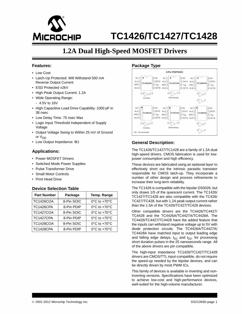
Package Type
General Description:
The TC1426/TC1427/TC1428 are a family of 1.2A dualhigh-speed drivers. CMOS fabrication is used for low-power consumption and high efficiency.
These devices are fabricated using an epitaxial layer toeffectively short out the intrinsic parasitic transistorresponsible for CMOS latch-up. They incorporate anumber of other design and process refinements toincrease their long-term reliability.
The TC1426 is compatible with the bipolar DS0026, butonly draws 1/5 of the quiescent current. The TC1426/TC1427/TC1428 are also compatible with the TC426/TC427/TC428, but with 1.2A peak output current ratherthan the 1.5A of the TC426/TC427/TC428 devices.
Other compatible drivers are the TC4426/TC4427/TC4428 and the TC4426A/TC4427A/TC4428A. TheTC4426/TC4427/TC4428 have the added feature thatthe inputs can withstand negative voltage up to 5V withdiode protection circuits. The TC4426A/TC4427A/TC4428A have matched input to output leading edgeand falling edge delays, tD1 and tD2, for processingshort duration pulses in the 25 nanoseconds range. Allof the above drivers are pin compatible.
The high-input impedance TC1426/TC1427/TC1428drivers are CMOS/TTL input-compatible, do not requirethe speed-up needed by the bipolar devices, and canbe directly driven by most PWM ICs.
This family of devices is available in inverting and non-inverting versions. Specifications have been optimizedto achieve low-cost and high-performance devices,well-suited for the high-volume manufacturer.
Part Number Package Temp. Range
TC1426COA 8-Pin SOIC 0°C to +70°C
TC1426CPA 8-Pin PDIP 0°C to +70°C
TC1427COA 8-Pin SOIC 0°C to +70°C
TC1427CPA 8-Pin PDIP 0°C to +70°C
TC1428COA 8-Pin SOIC 0°C to +70°C
TC1428CPA 8-Pin PDIP 0°C to +70°C
TC1426CPA
1
2
3
4
NC
5
6
7
8
OUT A
OUT B
NC
IN A
GND
IN B
VDD
2, 4 7, 5
Inverting
TC1427CPA
1
2
3
4
NC
5
6
7
8
OUT A
OUT B
NC
IN A
GND
IN B
2, 4 7, 5
Noninverting
TC1428CPA
1
2
3
4
NC
5
6
7
8
OUT A
OUT B
NC
IN A
GND
IN B
2 7
4 5
VDD VDD
TC1426COA
1
2
3
4
NC
5
6
7
8
OUT A
OUT B
NC
IN A
GND
IN B
VDD
NC = No connection
2, 4 7, 5
Inverting
TC1427COA
1
2
3
4
NC
5
6
7
8
OUT A
OUT B
NC
IN A
GND
IN B
2, 4 7, 5
Noninverting
TC1428COA
1
2
3
4
NC
5
6
7
8
OUT A
OUT B
NC
IN A
GND
IN B
2 7
4 5
VDD VDD
8-Pin PDIP/SOIC
2001-2012 Microchip Technology Inc. DS21393D-page 1

TC1426/TC1427/TC1428
Functional Block Diagram
Input
V+
≈2.5 μA
≈500 μA
NOTE: TC1428 has one inverting and one noninverting driver.Ground any unused driver input.
InvertingOutput
NoninvertingOutput
(TC1426)(TC1427)
GND
TC1426 InvertingTC1427 Noninverting
TC1428 Inverting/Noninverting
DS21393D-page 2 2001-2012 Microchip Technology Inc.

TC1426/TC1427/TC1428
1.0 ELECTRICAL CHARACTERISTICS
Absolute Maximum Ratings*
Supply Voltage .....................................................+18V
Input Voltage, Any Terminal ...................................VDD + 0.3V to GND – 0.3V
Power Dissipation (TA 70°C) PDIP........................................................ 730 mW SOIC ....................................................... 470 mW
Derating Factor PDIP....................................................... 8 mW/C SOIC ...................................................... 4 mW/C
Operating Temperature Range C Version ........................................ 0°C to +70°C
Storage Temperature Range.............. -65°C to +150°C
*Stresses above those listed under "AbsoluteMaximum Ratings" may cause permanent damage tothe device. These are stress ratings only and functionaloperation of the device at these or any other conditionsabove those indicated in the operation sections of thespecifications is not implied. Exposure to AbsoluteMaximum Rating conditions for extended periods mayaffect device reliability.
TC1426/TC1427/TC1428 ELECTRICAL SPECIFICATIONS
Electrical Characteristics: TA = +25°C, with 4.5V VDD16V, unless otherwise noted.
Symbol Parameter Min Typ Max Units Test Conditions
Input
VIH Logic 1, High Input Voltage 3 — — V
VIL Logic 0, Low Input Voltage — — 0.8 V
IIN Input Current -1 — 1 A 0VVINVDD
Output
VOH High Output Voltage VDD – 0.025 — — V Figure 3-1, Figure 3-2
VOL Low Output Voltage — — 0.025 V Figure 3-1, Figure 3-2
RO Output Resistance ——
128
1812
IOUT = 10 mA, VDD = 16V
IPK Peak Output Current — 1.2 — A
IREV Latch-Up CurrentWithstand Reverse Current
— >500 — mA
Switching Time (Note 1)
tR Rise Time — — 35 nsec Figure 3-1, Figure 3-2
tF Fall Time — — 25 nsec Figure 3-1, Figure 3-2
tD1 Delay Time — — 75 nsec Figure 3-1, Figure 3-2
tD2 Delay Time — — 75 nsec Figure 3-1, Figure 3-2
Power Supply
IS Power Supply Current ——
——
90.5
mA VIN = 3V (Both Inputs)VIN = 0V (Both Inputs)
Note 1: Switching times ensured by design.
2001-2012 Microchip Technology Inc. DS21393D-page 3

TC1426/TC1427/TC1428
TC1426/TC1427/TC1428 ELECTRICAL SPECIFICATIONS (CONTINUED)Electrical Characteristics: Over operating temperature range with 4.5V VDD16V, unless otherwise noted.
Symbol Parameter Min Typ Max Units Test Conditions
Input
VIH Logic 1, High Input Voltage 3 — — V
VIL Logic 0, Low Input Voltage — — 0.8 V
IIN Input Current -10 — 10 A 0VVINVDD
Output
VOH High Output Voltage VDD – 0.025 — — V Figure 3-1, Figure 3-2
VOL Low Output Voltage — — 0.025 V Figure 3-1, Figure 3-2
RO Output Resistance ——
1510
2318
IOUT = 10 mA, VDD = 16V
IREV Latch-Up CurrentWithstand Reverse Current
— >500 — mA
Switching Time (Note 1)
tR Rise Time — — 60 nsec Figure 3-1, Figure 3-2
tF Fall Time — — 40 nsec Figure 3-1, Figure 3-2
tD1 Delay Time — — 125 nsec Figure 3-1, Figure 3-2
tD2 Delay Time — — 125 nsec Figure 3-1, Figure 3-2
Power Supply
IS Power Supply Current ——
——
130.7
mA VIN = 3V (Both Inputs)VIN = 0V (Both Inputs)
Note 1: Switching times ensured by design.
DS21393D-page 4 2001-2012 Microchip Technology Inc.

TC1426/TC1427/TC1428
2.0 PIN DESCRIPTIONS
The descriptions of the pins are listed in Table 2-1.
TABLE 2-1: PIN FUNCTION TABLE
Pin No.(8-Pin PDIP,
SOIC)Symbol Description
1 NC No connection.
2 IN A Control input A, TTL/CMOS compatible logic input.
3 GND Ground.
4 IN B Control input B, TTL/CMOS compatible logic input.
5 OUT B Output B, CMOS totem-pole output.
6 VDD Supply input, 4.5V to 16V.
7 OUT A Output A, CMOS totem-pole output.
8 NC No connection.
2001-2012 Microchip Technology Inc. DS21393D-page 5

TC1426/TC1427/TC1428
3.0 APPLICATIONS INFORMATION
3.1 SUPPLY BYPASSING
Large currents are required to charge and dischargecapacitive loads quickly. For example, charging a 1000pF load to 16V in 25 nsec requires a 0.8A current fromthe device's power supply.
To ensure low supply impedance over a wide frequencyrange, a parallel capacitor combination is recom-mended for supply bypassing. Low-inductance ceramicMLC capacitors with short lead lengths (<0.5-in.)should be used. A 1.0 F film capacitor in parallel withone or two 0.1 F ceramic MLC capacitors normallyprovides adequate bypassing.
3.2 GROUNDING
The TC1426 and TC1428 contain inverting drivers.Individual ground returns for the input and outputcircuits or a ground plane should be used. This willreduce negative feedback that causes degradation inswitching speed characteristics.
FIGURE 3-1: Inverting Driver Switching Time
3.3 INPUT STAGE
The input voltage level changes the no-load orquiescent supply current. The N-channel MOSFETinput stage transistor drives a 2.5 mA current sourceload. With a logic ‘1’ input, the maximum quiescentsupply current is 9 mA. Logic ‘0’ input level signalsreduce quiescent current to 500 A maximum. Unuseddriver inputs must be connected to VDD or GND.Minimum power dissipation occurs for logic ‘0’ inputsfor the TC1426/TC1427/TC1428.
The drivers are designed with 100 mV of hysteresis.This provides clean transitions and minimizes outputstage current spiking when changing states. Inputvoltage thresholds are approximately 1.5V, making alogic ‘1’ input any voltage greater than 1.5V up to VDD.Input current is less than 1 A over this range.
The TC1426/TC1427/TC1428 may be directly drivenby the TL494, SG1526/27, TC38C42, TC170 andsimilar switch-mode power supply integrated circuits.
FIGURE 3-2: Noninverting Driver Switching Time
+5V
10%
90%
10%
90%
10%
90%VDD
1 μFWIMAMKS-2
0V
0V
TC1426(1/2 TC1428)
1
2
Test Circuit
0.1 μF MLC
Input
VDD = 16V
Output
tR
CL = 1000 pF
tD1tF
tD2
Input
Output
VDD
0.1 μF MLC
Input
VDD = 16V
Output
tR
CL = 1000 pF
tD1tF
tD2
Input
Output
90%
10%
10% 10%
90%
1 μFWIMAMKS-2
TC1427(1/2 TC1428)
+5V
0V
0V
90%
Test Circuit
1
2
DS21393D-page 6 2001-2012 Microchip Technology Inc.

TC1426/TC1427/TC1428
4.0 TYPICAL CHARACTERISTICS
Note: The graphs and tables provided following this note are a statistical summary based on a limited number ofsamples and are provided for informational purposes only. The performance characteristics listed hereinare not tested or guaranteed. In some graphs or tables, the data presented may be outside the specifiedoperating range (e.g., outside specified power supply range) and therefore outside the warranted range.
550
440
330
220
110
05 7 9 11 13 15
TIM
E (n
sec)
VDD (V)
10,000 pF
4700 pF
2200 pF
Rise Time vs. Supply Voltage330
264
198
132
66
0
TIM
E (n
sec)
10,000 pF
2200 pF
4700 pF
5 7 9 11 13 15
Fall Time vs. Supply Voltage
tD1TIM
E (n
sec)
5 7 9 11 13 15
80
70
60
50
40
30
Delay Time vs. Supply Voltage
TA = +25°C TA = +25°CCL = 1000 pFTA = +25°C
VDD (V) VDD (V)
tD2
40
32
24
16
8
025 45 65 85 105 125
TEMPERATURE (°C)
TIM
E (n
sec)
Rise and Fall Times vs. Temperature60
54
48
42
36
025 45 65 85 105 125
TEMPERATURE (°C)
TIM
E (n
sec)
Delay Time vs. Temperature30
24
18
12
6
0100 520 940 1360 1780 2200
SUPP
LY C
UR
REN
T (m
A)
CAPACITIVE LOAD (pF)
500 kHz
200 kHz
20 kHz
Supply Current vs. Capacitive Load
CL = 1000 pFVDD = +15VTA = +25°C
CL = 1000 pFVDD = +15V
CL = 1000 pFVDD = +15V
tD1
tD2tFALL
tRISE
CAPACITIVE LOAD (pF)100 1000 10,000
1000
100
10
10 VDD
TIM
E (n
sec) 5 VDD
15 VDD
Rise Time vs. Capacitive Load1000
100
10100 1000 10,000
CAPACITIVE LOAD (pF)
TIM
E (n
sec)
5 VDD
10 VDD
Fall Time vs. Capacitive Load
15VDD
100
80
60
40
20
010 100 1000 10,000
VDD = 15V
VDD = 10V
V = 5VDD
FREQUENCY (kHz)
SUPP
LY C
UR
REN
T (m
A)
Supply Current vs. Frequency
CL = 1000 pFTA = +25°CTA = +25°C TA = +25°C
2001-2012 Microchip Technology Inc. DS21393D-page 7

TC1426/TC1427/TC1428
TYPICAL CHARACTERISTICS (CONTINUED)
100 mA
50 mA
10 mA
15
13
11
9
7
55 7 9 11 13 15
OU
T(Ω
)R
Low-State Output Resistance50
42
34
26
18
105 7 9 11 13 15
100 mA
50 mA
10 mA
High-State Output Resistance
RO
UT
(Ω)
10-8
A (s
ec)
10-9
10-104 6 8 10 12 14 16 18
Crossover Energy Loss
TA = +25°C TA = +25°C
VDD (V) VDD (V) VDD (V)
20
15
10
5
0
0 50 100 150 200 300 400
SU
PPLY
VO
LTA
GE
(V)
SUPPLY CURRENT (μA)
Quiescent Power SupplyCurrent vs. Supply Voltage
BOTH INPUTS LOGIC ‘0’20
15
10
5
01 2 3 4 5 6
SUPP
LY V
OLT
AG
E (V
)
SUPPLY CURRENT (mA)
BOTH INPUTS LOGIC ‘1’
Quiescent Power SupplyCurrent vs. Supply Voltage
200
0
400
600
800
1000
1200
1400
1600
0 10 20 30 40 50 60 70 80 90 100 110 120AMBIENT TEMPERATURE (°C)
MA
X. P
OW
ER (m
W)
8 Pin DIP
Thermal Derating Curves
8 Pin SOIC
DS21393D-page 8 2001-2012 Microchip Technology Inc.

TC1426/TC1427/TC1428
5.0 PACKAGING INFORMATION
5.1 Package Marking Information
Package marking data not available at this time.
5.2 Taping Form
2001-2012 Microchip Technology Inc. DS21393D-page 9

TC1426/TC1427/TC1428
5.3 Package Dimensions
3° Min.
Pin 1
.260 (6.60)
.240 (6.10)
.045 (1.14)
.030 (0.76).070 (1.78).040 (1.02)
.400 (10.16).348 (8.84)
.200 (5.08)
.140 (3.56)
.150 (3.81)
.115 (2.92)
.110 (2.79)
.090 (2.29).022 (0.56).015 (0.38)
.040 (1.02)
.020 (0.51) .015 (0.38).008 (0.20)
.310 (7.87)
.290 (7.37)
.400 (10.16).310 (7.87)
8-Pin Plastic DIP
Dimensions: inches (mm)
Note: For the most current package drawings, please see the Microchip Packaging Specification locatedat http://www.microchip.com/packaging
DS21393D-page 10 2001-2012 Microchip Technology Inc.

TC1426/TC1427/TC1428
.050 (1.27) Typ.
8° Max.
Pin 1
.244 (6.20)
.228 (5.79).157 (3.99).150 (3.81)
.197 (5.00)
.189 (4.80)
.020 (0.51)
.013 (0.33).010 (0.25).004 (0.10)
.069 (1.75)
.053 (1.35) .010 (0.25).007 (0.18)
.050 (1.27)
.016 (0.40)
8-Pin SOIC
Dimensions: inches (mm)
Note: For the most current package drawings, please see the Microchip Packaging Specification locatedat http://www.microchip.com/packaging
2001-2012 Microchip Technology Inc. DS21393D-page 11

TC1426/TC1427/TC1428
6.0 REVISION HISTORY
Revision D (December 2012)
Added a note to each package outline drawing.
DS21393D-page 12 2001-2012 Microchip Technology Inc.

TC1426/TC1427/TC1428
THE MICROCHIP WEB SITE
Microchip provides online support via our WWW site atwww.microchip.com. This web site is used as a meansto make files and information easily available tocustomers. Accessible by using your favorite Internetbrowser, the web site contains the followinginformation:
• Product Support – Data sheets and errata, application notes and sample programs, design resources, user’s guides and hardware support documents, latest software releases and archived software
• General Technical Support – Frequently Asked Questions (FAQ), technical support requests, online discussion groups, Microchip consultant program member listing
• Business of Microchip – Product selector and ordering guides, latest Microchip press releases, listing of seminars and events, listings of Microchip sales offices, distributors and factory representatives
CUSTOMER CHANGE NOTIFICATION SERVICE
Microchip’s customer notification service helps keepcustomers current on Microchip products. Subscriberswill receive e-mail notification whenever there arechanges, updates, revisions or errata related to aspecified product family or development tool of interest.
To register, access the Microchip web site atwww.microchip.com. Under “Support”, click on“Customer Change Notification” and follow theregistration instructions.
CUSTOMER SUPPORT
Users of Microchip products can receive assistancethrough several channels:
• Distributor or Representative
• Local Sales Office
• Field Application Engineer (FAE)
• Technical Support
Customers should contact their distributor,representative or field application engineer (FAE) forsupport. Local sales offices are also available to helpcustomers. A listing of sales offices and locations isincluded in the back of this document.
Technical support is available through the web siteat: http://microchip.com/support
2001-2012 Microchip Technology Inc. DS21393D-page 13
TC1426/TC1427/TC1428
READER RESPONSE
It is our intention to provide you with the best documentation possible to ensure successful use of your Microchipproduct. If you wish to provide your comments on organization, clarity, subject matter, and ways in which ourdocumentation can better serve you, please FAX your comments to the Technical Publications Manager at(480) 792-4150.
Please list the following information, and use this outline to provide us with your comments about this document.
TO: Technical Publications Manager
RE: Reader ResponseTotal Pages Sent ________
From: Name
Company
Address
City / State / ZIP / Country
Telephone: (_______) _________ - _________
Application (optional):
Would you like a reply? Y N
Device: Literature Number:
Questions:
FAX: (______) _________ - _________
DS21393DTC1426/TC1427/TC1428
1. What are the best features of this document?
2. How does this document meet your hardware and software development needs?
3. Do you find the organization of this document easy to follow? If not, why?
4. What additions to the document do you think would enhance the structure and subject?
5. What deletions from the document could be made without affecting the overall usefulness?
6. Is there any incorrect or misleading information (what and where)?
7. How would you improve this document?
DS21393D-page 14 2001-2012 Microchip Technology Inc.
Note the following details of the code protection feature on Microchip devices:
• Microchip products meet the specification contained in their particular Microchip Data Sheet.
• Microchip believes that its family of products is one of the most secure families of its kind on the market today, when used in the intended manner and under normal conditions.
• There are dishonest and possibly illegal methods used to breach the code protection feature. All of these methods, to our knowledge, require using the Microchip products in a manner outside the operating specifications contained in Microchip’s Data Sheets. Most likely, the person doing so is engaged in theft of intellectual property.
• Microchip is willing to work with the customer who is concerned about the integrity of their code.
• Neither Microchip nor any other semiconductor manufacturer can guarantee the security of their code. Code protection does not mean that we are guaranteeing the product as “unbreakable.”
Code protection is constantly evolving. We at Microchip are committed to continuously improving the code protection features of ourproducts. Attempts to break Microchip’s code protection feature may be a violation of the Digital Millennium Copyright Act. If such actsallow unauthorized access to your software or other copyrighted work, you may have a right to sue for relief under that Act.
Information contained in this publication regarding deviceapplications and the like is provided only for your convenienceand may be superseded by updates. It is your responsibility toensure that your application meets with your specifications.MICROCHIP MAKES NO REPRESENTATIONS ORWARRANTIES OF ANY KIND WHETHER EXPRESS ORIMPLIED, WRITTEN OR ORAL, STATUTORY OROTHERWISE, RELATED TO THE INFORMATION,INCLUDING BUT NOT LIMITED TO ITS CONDITION,QUALITY, PERFORMANCE, MERCHANTABILITY ORFITNESS FOR PURPOSE. Microchip disclaims all liabilityarising from this information and its use. Use of Microchipdevices in life support and/or safety applications is entirely atthe buyer’s risk, and the buyer agrees to defend, indemnify andhold harmless Microchip from any and all damages, claims,suits, or expenses resulting from such use. No licenses areconveyed, implicitly or otherwise, under any Microchipintellectual property rights.
2001-2012 Microchip Technology Inc.
QUALITY MANAGEMENT SYSTEM CERTIFIED BY DNV
== ISO/TS 16949 ==
Trademarks
The Microchip name and logo, the Microchip logo, dsPIC, FlashFlex, KEELOQ, KEELOQ logo, MPLAB, PIC, PICmicro, PICSTART, PIC32 logo, rfPIC, SST, SST Logo, SuperFlash and UNI/O are registered trademarks of Microchip Technology Incorporated in the U.S.A. and other countries.
FilterLab, Hampshire, HI-TECH C, Linear Active Thermistor, MTP, SEEVAL and The Embedded Control Solutions Company are registered trademarks of Microchip Technology Incorporated in the U.S.A.
Silicon Storage Technology is a registered trademark of Microchip Technology Inc. in other countries.
Analog-for-the-Digital Age, Application Maestro, BodyCom, chipKIT, chipKIT logo, CodeGuard, dsPICDEM, dsPICDEM.net, dsPICworks, dsSPEAK, ECAN, ECONOMONITOR, FanSense, HI-TIDE, In-Circuit Serial Programming, ICSP, Mindi, MiWi, MPASM, MPF, MPLAB Certified logo, MPLIB, MPLINK, mTouch, Omniscient Code Generation, PICC, PICC-18, PICDEM, PICDEM.net, PICkit, PICtail, REAL ICE, rfLAB, Select Mode, SQI, Serial Quad I/O, Total Endurance, TSHARC, UniWinDriver, WiperLock, ZENA and Z-Scale are trademarks of Microchip Technology Incorporated in the U.S.A. and other countries.
SQTP is a service mark of Microchip Technology Incorporated in the U.S.A.
GestIC and ULPP are registered trademarks of Microchip Technology Germany II GmbH & Co. & KG, a subsidiary of Microchip Technology Inc., in other countries.
All other trademarks mentioned herein are property of their respective companies.
© 2001-2012, Microchip Technology Incorporated, Printed in the U.S.A., All Rights Reserved.
Printed on recycled paper.
ISBN: 9781620767887
Microchip received ISO/TS-16949:2009 certification for its worldwide
DS21393D-page 15
headquarters, design and wafer fabrication facilities in Chandler and Tempe, Arizona; Gresham, Oregon and design centers in California and India. The Company’s quality system processes and procedures are for its PIC® MCUs and dsPIC® DSCs, KEELOQ® code hopping devices, Serial EEPROMs, microperipherals, nonvolatile memory and analog products. In addition, Microchip’s quality system for the design and manufacture of development systems is ISO 9001:2000 certified.

DS21393D-page 16 2001-2012 Microchip Technology Inc.
AMERICASCorporate Office2355 West Chandler Blvd.Chandler, AZ 85224-6199Tel: 480-792-7200 Fax: 480-792-7277Technical Support: http://www.microchip.com/supportWeb Address: www.microchip.com
AtlantaDuluth, GA Tel: 678-957-9614 Fax: 678-957-1455
BostonWestborough, MA Tel: 774-760-0087 Fax: 774-760-0088
ChicagoItasca, IL Tel: 630-285-0071 Fax: 630-285-0075
ClevelandIndependence, OH Tel: 216-447-0464 Fax: 216-447-0643
DallasAddison, TX Tel: 972-818-7423 Fax: 972-818-2924
DetroitFarmington Hills, MI Tel: 248-538-2250Fax: 248-538-2260
IndianapolisNoblesville, IN Tel: 317-773-8323Fax: 317-773-5453
Los AngelesMission Viejo, CA Tel: 949-462-9523 Fax: 949-462-9608
Santa ClaraSanta Clara, CA Tel: 408-961-6444Fax: 408-961-6445
TorontoMississauga, Ontario, CanadaTel: 905-673-0699 Fax: 905-673-6509
ASIA/PACIFICAsia Pacific OfficeSuites 3707-14, 37th FloorTower 6, The GatewayHarbour City, KowloonHong KongTel: 852-2401-1200Fax: 852-2401-3431
Australia - SydneyTel: 61-2-9868-6733Fax: 61-2-9868-6755
China - BeijingTel: 86-10-8569-7000 Fax: 86-10-8528-2104
China - ChengduTel: 86-28-8665-5511Fax: 86-28-8665-7889
China - ChongqingTel: 86-23-8980-9588Fax: 86-23-8980-9500
China - HangzhouTel: 86-571-2819-3187 Fax: 86-571-2819-3189
China - Hong Kong SARTel: 852-2943-5100 Fax: 852-2401-3431
China - NanjingTel: 86-25-8473-2460Fax: 86-25-8473-2470
China - QingdaoTel: 86-532-8502-7355Fax: 86-532-8502-7205
China - ShanghaiTel: 86-21-5407-5533 Fax: 86-21-5407-5066
China - ShenyangTel: 86-24-2334-2829Fax: 86-24-2334-2393
China - ShenzhenTel: 86-755-8864-2200 Fax: 86-755-8203-1760
China - WuhanTel: 86-27-5980-5300Fax: 86-27-5980-5118
China - XianTel: 86-29-8833-7252Fax: 86-29-8833-7256
China - XiamenTel: 86-592-2388138 Fax: 86-592-2388130
China - ZhuhaiTel: 86-756-3210040 Fax: 86-756-3210049
ASIA/PACIFICIndia - BangaloreTel: 91-80-3090-4444 Fax: 91-80-3090-4123
India - New DelhiTel: 91-11-4160-8631Fax: 91-11-4160-8632
India - PuneTel: 91-20-2566-1512Fax: 91-20-2566-1513
Japan - OsakaTel: 81-66-152-7160 Fax: 81-66-152-9310
Japan - YokohamaTel: 81-45-471- 6166 Fax: 81-45-471-6122
Korea - DaeguTel: 82-53-744-4301Fax: 82-53-744-4302
Korea - SeoulTel: 82-2-554-7200Fax: 82-2-558-5932 or 82-2-558-5934
Malaysia - Kuala LumpurTel: 60-3-6201-9857Fax: 60-3-6201-9859
Malaysia - PenangTel: 60-4-227-8870Fax: 60-4-227-4068
Philippines - ManilaTel: 63-2-634-9065Fax: 63-2-634-9069
SingaporeTel: 65-6334-8870Fax: 65-6334-8850
Taiwan - Hsin ChuTel: 886-3-5778-366Fax: 886-3-5770-955
Taiwan - KaohsiungTel: 886-7-213-7828Fax: 886-7-330-9305
Taiwan - TaipeiTel: 886-2-2508-8600 Fax: 886-2-2508-0102
Thailand - BangkokTel: 66-2-694-1351Fax: 66-2-694-1350
EUROPEAustria - WelsTel: 43-7242-2244-39Fax: 43-7242-2244-393Denmark - CopenhagenTel: 45-4450-2828 Fax: 45-4485-2829
France - ParisTel: 33-1-69-53-63-20 Fax: 33-1-69-30-90-79
Germany - MunichTel: 49-89-627-144-0 Fax: 49-89-627-144-44
Italy - Milan Tel: 39-0331-742611 Fax: 39-0331-466781
Netherlands - DrunenTel: 31-416-690399 Fax: 31-416-690340
Spain - MadridTel: 34-91-708-08-90Fax: 34-91-708-08-91
UK - WokinghamTel: 44-118-921-5869Fax: 44-118-921-5820
Worldwide Sales and Service
11/27/12
Recommended