1 High-Speed Interfaces
In addition to computers, other home information
appliances have also become more advanced, and internet
connections are now available for AV equipment, so interfaces
that can handle digital information with low signal deterioration
have become more important.
This will explain methods for EMC countermeasures on
high-speed interface signals, which have become more common
for computers and information appliances.
Common High-Speed Interfaces
USB: USB is used for connecting computers with peripheral
devices (such as CD-ROMs, scanners, printers, and DSCs)
(Figure 1). In 2000, the USB 2.0 standard was implemented,
which made three transfer speeds available; LS (1.5 Mbps), FS
(12 Mbps), and HS (480 Mbps), which allows for DSC image
data to be transferred at high speeds (Photo 1).
Digital audio devices use USB as the standard interface for
transferring audio files from computers downloaded from the
internet.
Recently, video contents can also be viewed by mobile
devices in addition to audio files, making it necessary to have
faster transfer speeds.
In 2008, “USB 3.0” was released, allowing for a transfer
speed of 5 Gbps based on the demand mentioned above.
There is a demand for distributing large-size video contents, so
this new standard has potential to be more common on mobile
phones and digital audio devices in addition to computers.
Therefore, this interface merits close attention.
EMC countermeasures for High-Speed Differential InterfacesTDK EMC Technology Practice Section
TDK Corporation Application Center
Masao Umemura
How Do Common Mode Filters Suppress EMI in Differential Transmission Circuits?
Photo 1 What is USB?
Photo 2 What is IEEE?
Figure 1 USB and IEEE1394 Equipment Used

IEEE1394: IEEE1394 is an interface that was initiated by Apple
Computer, which calls it Firewire, and was adopted by the IEEE
and has become more common (Figure 1, Photo 2). This is a
standard interface for video related devices such as flat panel
TVs, DVD recorders, and DVCs with practical use speeds
ranging from 100 to 800 Mbps.
The roadmap for the IEEE interface has been set to
achieve speeds of up to 3.2 Gbps, so higher speed
communication will be available in the future. With few
exceptions, IEEE does not require the concept of a HOST.
High-speed transferring and recording of MPEG signals
between AV devices is possible using simple remote control
operation. The directional movement for this interface is half
duplex.
DVI / HDMI: DVI and HDMI interfaces are used for sending
digitized image signals output from a computer to a monitor,
which used to be done using analog RGB data. These
interfaces allow for uncompressed digital video signals to be
transferred at high speeds. The TMDS method is used and the
maximum speed is 1.65 Gbps, with the transfer frequency
generally reaching 850 MHz. With DVI, only video signals can
be transferred (Figure 2).
With HDMI, in addition DVI video signals, audio signals can
be sent simultaneously when connected to AV devices. HDMI
also allows for copyright protection, and in the United States,
digital TVs must be equipped with HDMI inputs. This interface
has quickly become widespread (Figure 3). The directionality
for this interface is one directional from the HOST to the
TARGET.
S-ATA: S-ATA is an interface used for computer HDDs which
has come to replace the IDE method. Serial ATA is used
because of the demand for a high-speed interface to handle
large amounts of data (Figure 4). The speed for S-ATA is 3
Gbps, and can be sorted into classes based on the usage
purpose, such as for internal connections or external HDDs.
There are different voltages used for transferring data. The
directionality is half-duplex.
DisplayPort: Whereas HDMI is the standard digital interface for
AV device connections, DisplayPort is an interface for
connecting computers with monitors. DVI has been used as an
interface for connecting computers and monitors, but it seems
that this will be replaced by DisplayPort because it is smaller
and capable of higher transfer speeds.
DisplayPort contains four “Lanes” of differential pair line.
There are two link rate modes for each lane; 1.62 Gbps (Low bit
rate) and 2.7 Gbps (High bit rate). In addition, with DisplayPort,
the clock signal is embedded in the data signal, so there is no
clock line as with HDMI / LVDS. Therefore, the maximum
transfer rate is 10.8 Gbps (2.7 Gbps × 4), making is compatible
with resolutions of QXGA (2048 × 1536) and higher.
The standard frequency during 2.7 Gbps transfer is 1.35
GHz, which places it in the GHz range. In the past, most noise
problems with high-speed interfaces were related to the band
below 1 GHz. However, with DisplayPort, the standard
frequency noise spectrum exists in the GHz band, so it is
necessary to verify interference problems related to wireless
applications.
PCI-Express for internal computer bus connections, and
Infiniband for connecting servers, which operate at over 3 Gbps,
have also been released as advanced interfaces. It is expected
that differential transfer methods will become more common as
interfaces capable of transferring signals at higher speeds while
minimizing the number of wires (Table 1).
Figure 2 DVI Interface (Panel Link) Usage Example
Figure 3 HDMI Interface Usage Example
Figure 4 S-ATA (Serial ATA) Usage Example
* HDMI: High Definition Multimedia Interface
* S-ATA: Serial AT Attachment
* DVI: Digital Visual Interface

2 What is Differential Transmission?
Various methods for transferring high-speed signals have
been proposed and have come to be used. In order to improve
EMC, this section will explain the differential transfer method,
which is commonly used for these interfaces.
The differential transfer method uses two signals that have
180° opposite phases, which is different from single line data
transfer. This transmission method is also referred to as
balanced transmission, which has a smaller amount of
unnecessary radiation than with the normal single-end
transmission method, and also has the characteristic that it is
more resistant to influence from other devices. However, in
reality, common mode noise is generated due to differential
signal unbalance, noise current leaks from other circuits on the
substrate to the outside through the connector, and noise is
radiated through the cable, which acts like an antenna.
In the above, it was explained that the unbalance of the
differential signal causes common mode noise, and this section
will explain more details about this unbalance. Figure 5 shows
ideal differential transmission and the signal waveform with
phase shifting between differential signals. The ideal common
mode voltage, which is expressed as the total of the two signals,
is linear. However, when the signal has poor symmetry among
the channels, unbalanced components are generated. This is
referred to as skew.
Figure 5 Differential Signal Unbalanced ComponentsD+ + D– (Common Mode Voltage)
Blowup of (a) Blowup of (b)
(b) Phase shifting (0.1 nsec.) (b) Phase shifting (0.1 nsec.)
(a) Ideal differential signal (a) Ideal differential signal
Differential Signal Waveform
USB 1.1 / USB 2.0 12 Mbps / 480 MbpsIEEE1394.a/b 400 Mbps / 800 MbpsLVDS 1.12 Gbps: UXGAMini-LVDS 1.12 Gbps: UXGARSDS 160 MbpsS-ATA I / II / III 1.5 Gbps / 3 Gbps / 6 GbpsDVI 1.65 Gbps: UXGAHDMI 3.4 Gbps: 1080 p / 16 bit gradationDisplayPort 2.7 GbpsPCI Express (I/II) 2.5 Gbps / 5 GbpsUSB 3.0 5 Gbps
Table 1 Common High-Speed Interface Types and Speeds

As shown in Figure 6, unbalanced components are also
generated by other unbalances such as differences in the rise
and fall times and differences in the pulse width and amplitude.
Unnecessary common mode radiation increases if the amplitude
of the unbalanced components is higher.
Common Mode Filters are components with 1:1 transformer
characteristics consisting of coupled coils between two
channels. The main purpose of these filters is to suppress
common mode current, but they are also effective for correcting
differential signal unbalance. When a signal is input to one
channel, the same signal is induced to the other channel so that
balance can be maintained between both lines.
As shown in Figure 7, the input voltages for the two
channels are expresses as V1 and –V2, and the output voltages
are expressed as V1out and –V2out. The output voltage is the
total of aV1 and –aV2 voltages that pass each channel, and the
total of the –bV1 and bV2 voltages that are induced.
This is shown in the following equations.
V1out = aV1 + bV2
V2out = -aV2 – bV1
The coefficients a and b include the coupling coefficients
between the channels, the common mode inductance, and the
termination resistance.
This is shown in the following.
Coupling Coefficient: K = 1,
When Common Mode Impedance Zc >> Termination
Resistance: Z0,
a = b = 1/2,
V1out = –V2out = V1/2 + V2/2
Therefore, when V1 and V2 are different, the absolute values of
the absolute voltages are equal.
Figure 8 shows the differential signal waveform for USB 2.0
HS (High Speed) mode. This shows that the unbalanced
component of the common mode voltage was corrected by
installing a Common Mode Filter. This shows the effectiveness
of reducing unnecessary common mode radiation. Based on
this result, it can be said that Common Mode Filters are effective
components for the EMC countermeasures of differential signal
lines.
The differential mode impedance of Common Mode Filters
can be reduced in the high-frequency band through magnetic
coupling of the channels. Therefore, there is no danger of
influencing high-speed differential signal waveform quality.
Common Mode Filters with high coupling are better because
they have lower differential mode impedance. Details regarding
the effectiveness of correcting skew will be explained in Chapter
4 using test results, which will help to show the how Common
Mode Filters can be used to reduce EMI.
Figure 6 Other Possible Causes of Unbalance
Figure 7 Advantages of Common Mode Filters

3 EMC Countermeasures for Gigabit Transfer Interfaces
DVI (Digital Visual Interface) and HDMI (High Definition
Multimedia Interface) are designed using high-speed TMDS
(Transition Minimized Differential Signaling) so that large
amounts of information such as HDTV video signals can be sent
without being compressed.
These interfaces are often used for multimedia devices
such as Digital TVs, computers, DVD players, STBs, DVD
recorders. Directionality is not bidirectional, and the circuit
configuration is for sending information one-way from the sender
to the receiver. The speed reaches up to 1.6 Gbps, and the
basic frequency reaches 800 MHz or higher. This frequency is
four to five greater than for USB and IEEE1394, so the details of
the requirements for signal quality are regulated (Figure 9).
For this purpose, the following are used.
Eye-patterns
Transmission Line Characteristic Impedance (Cables and
Wires on PCBs)
High-frequency (fifth to seventh order of 800 MHz) EMI can
occur, so it is important to implement countermeasures for
high-frequency EMI.
Figure 8 Differential Signal Unbalanced Components
Figure 9 HDMI Interface Connection Diagram
D+ + D− (Common Mode Voltage)
(b) Common Mode Filter Application Example (ACM2012-900-2P) (b) Common Mode Filter Application Example (ACM2012-900-2P)
(a) USB 2.0 device differential signal (a) USB 2.0 device differential signal
Differential Signal Waveform

This section will explain the characteristics of newly
developed Common Mode Filters for DVI, HDMI, and
DisplayPort, their influence on the signal, and their effectiveness
for EMI suppression.
1) Common mode filters for HDMI and DVI with 6 GHz cutoff
frequency and for DisplayPort with 8 GHz cutoff frequency
Common Mode Filters are used to suppress EMI by
installing them to interfaces that handle Gigabit signals. As
mentioned in the explanation for USB and IEEE1394, signal
quality is strongly affected. Because of this, it is necessary to
optimize the cutoff frequency for each interface based on the
insertion loss of the differential mode. As a result, it is possible
to transfer high-speed TMDS signals without causing strain.
With digital signal transmission, transmission is at least five
times (fifth order harmonics) that of the fundamental wave so
that signal quality can be maintained during transmission.
When Common Mode Filters (ACM-H and TCM-H Series)
are used for HDMI, 6 GHz cutoff frequency allows for fifth order
harmonics of 2.225 Gbps (about 1.1 GHz) to pass through
sufficiently at the 1080p Deep Color transfer rate, which means
the HDMI signal quality can be maintained. The cutoff
frequency of Common Mode Filters for DisplayPort (TCM-U
Series) was extended up to 8 GHz so that there is no signal
deterioration of 2.7 Gps signals (Figure 10 and Figure 11).
2) Eye-pattern
With HDMI, the Eye-pattern is regulated, so if the signal
contains strain, it cannot pass the standard. Common Mode
Filters for HDMI help to ensure the 6 GHz bandwidth so that
products can easily pass the Eye-pattern test. Figure 12 shows
the measurement conditions, and Figure 13 (a) shows the
measurement results for DVI.
Similarly, the Eye-pattern is also regulated for DisplayPort.
When a TCM1210U Series component for DisplayPort is used,
the 2.7 Gbps signal does not deteriorate. Figure 13 (b) shows
the eye diagram for the sending baseplate. Figure 13 (c) shows
the eye diagram for a 10 m cable. The Common Mode Filter did
not cause deterioration on the eye diagram with a 10 m cable,
which indicates that TCM1210U can be used to reduce noise
while maintaining signal quality.
Figure 10 Common Mode Filter for HDMI that Ensures the 6 GHz Band
Figure 11 High-band, High-Quality Winding Type CMF

3) Characteristic Impedance
HDMI standards regulate TDR (Time Domain
Reflectometry) characteristics. This regulates the characteristic
impedance for the transmission line so that high-speed signals
can be transmitted. The characteristic impedance for PCB
patterns equipped with ICs, cables mainly used for transmission
lines, and connectors for connections are set at 100 ±15 Ω. If a
Common Mode Filter not recommended for TMDS (or for DVI
and HDMI) is used on a TMDS line to suppress EMI, the product
will not meet this regulation. For HDMI, the test conditions for
regulating connectability will not be met (Compliance tests for
HDMI are regulated so that connectability can be guaranteed. If
this test is not passed, a product cannot be approved for as an
HDMI device.). Common Mode Filters for HDMI are design so
that the characteristic impedance between the lines is 100 Ω,
which means they can be used safely (Figure 14).
Figure 12 DVI (UXGA: 1.65 Gbps) Waveform Measurement Conditions
Figure 14
Figure 13(a) HDMI waveform
(c) DisplayPort waveform at receiving baseplate using 10m cable (2.7 Gbps during transmission)
(b) DisplayPort waveform at the sending baseplate (2.7 Gbps during transmission)

4) EMI Measurement Examples
Figure 15 shows an efficiency example of EMI suppression
for HDMI. Figure 16 shows a sample circuit using one of our
Common Mode Filters.
As with other interfaces, it is necessary to consider noise
radiation for DisplayPort. However, computers and monitors are
set as the target, so it is also necessary to consider noise
interference from wireless devices for computers that use
wireless signals such as WLAN and Bluetooth. This noise can
be effectively suppressed using Common Mode Filters. Figure
17 shows a measurement diagram for verifying the influence of
wireless devices. Figure 18 shows the measurement results.
A WLAN device was used for testing. Using IEEE802.11b at 2.4
GHz, it was confirmed that WLAN reception sensitivity differed
when noise suppression components were used and when they
were not used. By installing a filter, noise was reduced by about
2 to 3 dB.
In the past, noise countermeasures have been implemented
to meet FCC and CISPR noise standards. However, from now,
it is expected that countermeasures will need to be implemented
for electromagnetic noise, which affects the operation of
wireless devices.
Figure 15 Effectiveness of EMI Suppression for HDMI Devices Using an HDMI Filter
Figure 17 Verification of the Influence of DisplayPort on WLAN Devices (Measurement Conditions)
Figure 18 Verification of the Influence of DisplayPort on WLAN Devices (Measurement Conditions)
Figure 16 Similar Countermeasures Implemented to a Differential Line with a Total of 4 Pairs: Data Channel (3 Pairs) and Clock Signal (1 Pair)

4 How Do Common Mode Filters Suppress Differential Signal Noise?
As mentioned previously, the differential transmission
method is used for many devices. The following will explain
how Common Mode Filters can be used to suppress differential
signal EMI showing basic test results.
A signal generator was used instead of an actual IC in order
to simplify the tests, and an accurate signal was used where
skew was given to the differential signal, a Common Mode Filter
was installed on the differential line, and then efficiency was
verified.
IC output itself may already contain skew, and skew may
occur during differential signal transmission due to rise and fall
characteristic variation. In addition, when the differential signal
from the IC is transmitted by the PCB pattern and cables, the
difference in the distance to the receiver terminal may be viewed
as skew.
Figure 19 is a graph that shows the amount of difference
with the PCB pattern can cause skew at the frequency of the
differential transmission method that is normally used. The
necessary transmission time for skew to occur at 1% at each
frequency was calculated. For example, when a signal was
transmitted using DVI and HDMI at 800 MHz, the difference in
the pattern length was about 2 mm, and skew of about 1%
occurred. Therefore, a stricter pattern design is needed for
high-order harmonic components.
Figure 20 shows the devices and circuit diagram that were
used for testing. A pattern that can receive the differential signal
from the signal generator on the baseplate was prepared and
then the component was installed. A shielded cable about 1 m
long and with a characteristic impedance of 100 Ω was installed,
and it was terminated at 100 Ω. The waveform and EMI was
observed by changing the skew from 0 to 3% with a basic
frequency set at 100 MHz and amplitude set at 400 mV.
Figure 21-1 shows the waveform when skew was 0%. The
throughput was the waveform when no noise components were
used. ACM2012-201-2P is a Common Mode Filter often used
for USB and IEEE1392 for EMI countermeasures.
Measurements were also made when chip beads were used,
which are commonly used for EMI countermeasures on signals
other than differential signals.
The first waveform in Figure 21-1 is based on the
measurement of the differential signal using a single-end probe.
The second waveform is the measurement of the common
mode voltage with the differential signal added. If a voltage
occurs here, noise is radiated as EMI.
The third waveform in Figure 21-1 shows the difference of
differential signals, and this waveform is transferred as the input
of the receiver terminal IC. The second common mode voltage
needs to be given attention.
Figure 21-2 shows when approximately 1% skew is given to
the differential signal from the signal generator. A small amount
of common mode voltage was observed. However, the voltage
amount was according to the order: EMI Components > Chip
Beads > Common Mode Filter. The voltage was almost
nonexistent when a ACM2012 Common Mode Filter was used.
Figure 19 Frequency Characteristics Example
Figure 20 Diagram of Test Equipment and Circuit

This shows the effectiveness of Common Mode Filters for
correcting skew.
Figure 21-3 and Figure 21-4 show the waveforms when the
skew amount sent from the signal generator was increased to
2% and 3%. The amount of common mode voltage gradually
increased when no EMI components were used and when chip
beads were used. However, when a Common Mode Filter was
used, skew was corrected and the voltage was almost
nonexistent. Also, when chip beads were used, the differential
signal and the voltage magnitude of the signal at the receiver
terminal were affected, so it was found that crest value was
small.
Figure 21-1 Waveform Data when Skew was Impressed
Figure 21-2
Figure 21-3
Figure 21-4

Figure 22 shows a graph with the common mode voltage
changes plotted. When a Common Mode Filter is used, the
common mode voltage was almost nonexistent even when the
skew was large.
Figure 23 shows the measurement data for EMI radiation
characteristics when a 3-m anechoic chamber was used. It was
found that Common Mode Filters are very effective at
suppressing EMI.
Figure 24 shows a graph plotting the EMI radiation
characteristics based on odd-order harmonics including the
fundamental wave.
When chip beads were used, the amplitude of the
fundamental wave was affected, so EMI occurrence was smaller
than when a Common Mode Filter was used at 0%. When a
Common Mode Filter was used, it was transmitted without
deterioration of the waveform. Therefore, it was lower than
when no EMI components were used, but slightly higher
radiation characteristics were found than when chip beads were
used. Regarding the radiation characteristics from the third to
ninth order, the Common Mode Filter was able to reduce EMI
radiation up to the harmonics regardless of the amount of skew.
In this way, it was found that Common Mode Filters are
able to suppress EMI by effectively correcting skew.
This effectiveness can also be expected when used with
actual ICs. Therefore, Common Mode Filters are essential for
EMI countermeasures on differential signals, which will continue
to become faster.
Figure 25 and Figure 26 show examples of Common Mode
Filters.
Figure 22 Common Mode Voltage due to Skew
Figure 23 Effectiveness of Suppressing EMI

Figure 24 Effectiveness of Suppressing EMI at the Harmonics Spectrum
Figure 25 Common Mode Filter Example (1)
Shape / Dimensions and Recommended Land Pattern
Electrical Characteristics
ACM2012 Type
Part No. Impedance (Ω) typical [100 MHz]
DC resistance (Ω) max. [For 1 line]
Rated current Idc (A) max.
Rated voltage Edc (V) max.
Insulation resistance (MΩ) min.
ACM2012-900-2P 90 0.19 0.4 50 10ACM2012-121-2P 120 0.22 0.37 50 10ACM2012-201-2P 200 0.25 0.35 50 10ACM2012-361-2P 360 0.5 0.22 50 10ACM2012-102-2P 1000 1.1 0.1 50 10
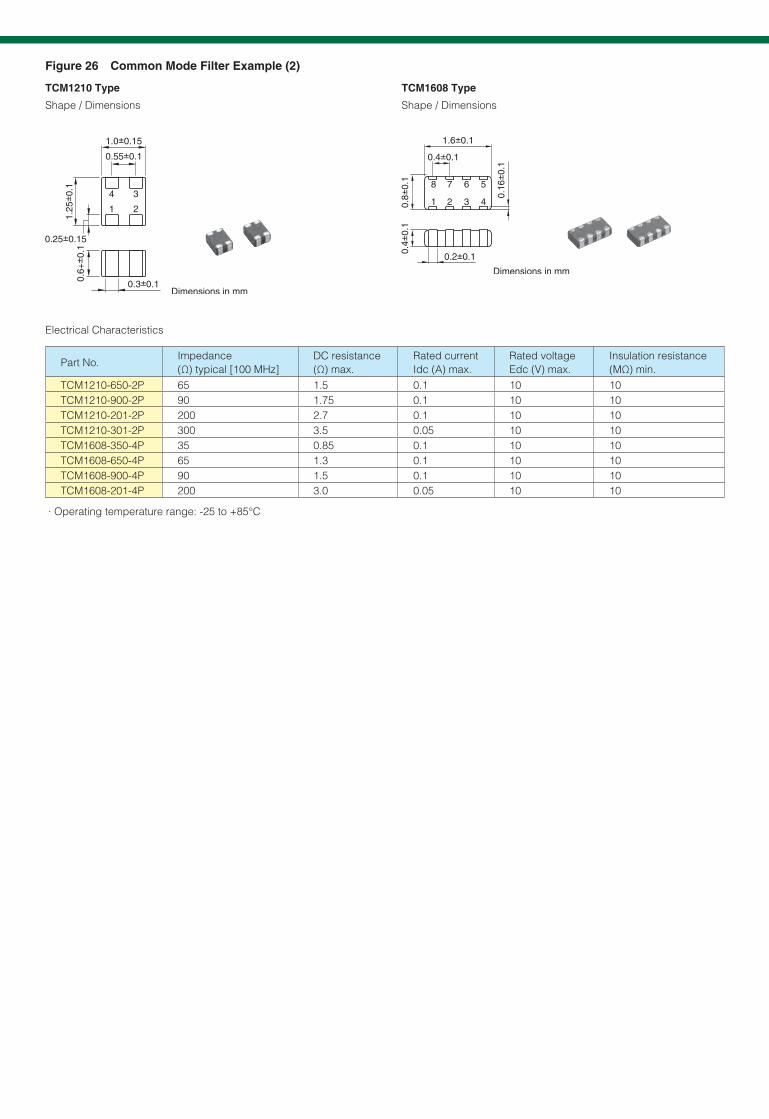
Figure 26 Common Mode Filter Example (2)
Shape / Dimensions Shape / Dimensions
TCM1210 Type TCM1608 Type
Part No.Impedance (Ω) typical [100 MHz]
DC resistance (Ω) max.
Rated currentIdc (A) max.
Rated voltageEdc (V) max.
Insulation resistance(MΩ) min.
TCM1210-650-2P 65 1.5 0.1 10 10TCM1210-900-2P 90 1.75 0.1 10 10TCM1210-201-2P 200 2.7 0.1 10 10TCM1210-301-2P 300 3.5 0.05 10 10TCM1608-350-4P 35 0.85 0.1 10 10TCM1608-650-4P 65 1.3 0.1 10 10TCM1608-900-4P 90 1.5 0.1 10 10TCM1608-201-4P 200 3.0 0.05 10 10
Electrical Characteristics
· Operating temperature range: -25 to +85°C
Recommended