THE OHIO STATE UNIVERSITY
The Design, Simulation, Verification and
Implementation of Vending Machine
Based on FPGA
Dept. of Electrical and Computer Engineering
The Ohio State University
2012
Advisor: Prof. Y. F. Zheng
By
Jialiang Zhang
05/10/2012
P a g e | 2
A B S T R A C T
Vending Machines or Vendors are more and more popular in modern society. Depending
on the high autonomous level, it can satisfy customers and complete the merchandise process
without any human labor input. And there are various vending machines with all different
functions available, but basically, they are all controlled and operated by middle to large scales
digital circuits. The purpose of this study is to apply the knowledge about the whole process of
digital circuit design, meaning coding, simulation, verification, synthesis and implementation to
design a general model of vending machine based on FPGA (Field Programmable Gate Array).
The vending machine model is written in VHDL (VHSIC Hardware Description Language), and
be implemented and tested on a Xilinx Spartan 3E FPGA development board.

P a g e | 3
ACKNOWLEDGMENT
I wish to thank my adviser, Professor Y. F. Zheng, for his support through my study and
research. And from the very beginning, it was in one of Professor Zheng’s lectures that I
originally got this idea and topic, and under his devotion of time and help, I was able to timely
complete the thesis and the project.
P a g e | 4
TABLE OF CONTENTS
Page
Abstract……………………………………………………………………………2
Acknowledgments………………………………………………………………...3
List of Tables……………………………………………………………………...7
List of Figures……………………………………………………………………..8
Chapters:
1. Introduction…………………………………………………………….......11
2. Design Proposal…………………………………………………………….12
3. System Controller Unit Design (Control Center) .…………………………13
3.1 Component Details………………………………………………….13
3.2 Design Process………………………………………………………16
3.3 Initial Design………………………………………………………...18
3.4 I/O Design Definitions………………………………………………19
3.5 Revised Design……………………………………………………...21
3.6 Initial Optimization………………………………………………….25
3.7 Machine Design with VHDL………………………………………..27
4. Simulation and Verification.……………………………………………….31
4.1 Preliminary Simulation……………………………………………...31
P a g e | 5
4.2 Complete Simulation and Verification……………………………...37
5. Top-Level and Peripheral Component Design……………………………..44
5.1 Top-Level Design and Modularization……………………………...44
5.2 Clock Divider Unit…………………………………………………..45
5.3 Asynchronous Pulse Generator Unit………………………………...47
6. User Interface Unit Design (Keypad and Display System)………………...50
6.1 Product Selection Unit (Keypad System)…………………...............50
6.2 Seven-Segment Display Unit (Display System)…………………….53
6.3 User Interface Unit Top-Level Design…………….………………...53
7. Final Vending Machine Design.…………………………………………....54
7.1 Clock Divider Unit (50 MHz to 1.5 KHz & 95 Hz)………………...54
7.2 Flag Signal Modification…………………………………………....55
7.3 Improved Four-Digit Seven-Segment Display Unit………………...56
7.4 Final Vending Machine Top-Level Design…………………………57
8. Synthesis…………………………………………………………………....58
9. Implementation……………………………………………………………..61
10. Program FPGA…………….………………………………………………63
11. Conclusion…………………………………………………………………65
12. References…………………………………………………………………66
P a g e | 6
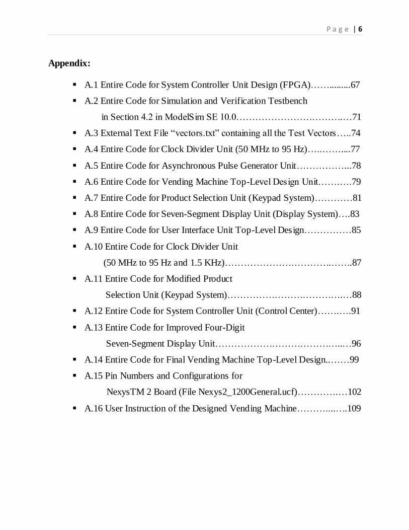
Appendix:
A.1 Entire Code for System Controller Unit Design (FPGA)…….........67
A.2 Entire Code for Simulation and Verification Testbench
in Section 4.2 in ModelSim SE 10.0…………………………….…71
A.3 External Text File “vectors.txt” containing all the Test Vectors…..74
A.4 Entire Code for Clock Divider Unit (50 MHz to 95 Hz)…..……....77
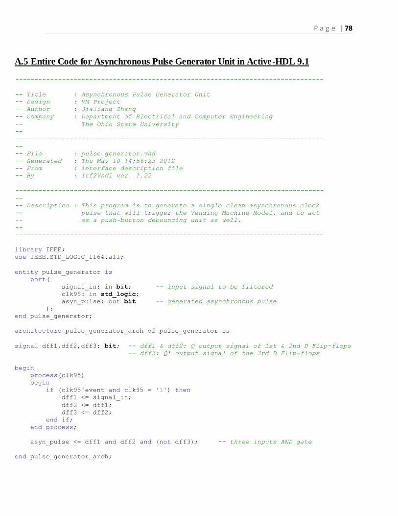
A.5 Entire Code for Asynchronous Pulse Generator Unit……………...78
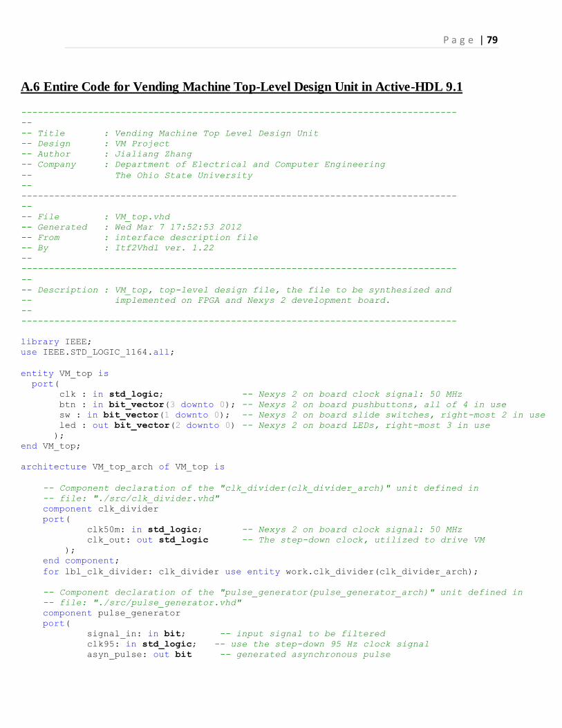
A.6 Entire Code for Vending Machine Top-Level Design Unit…….….79
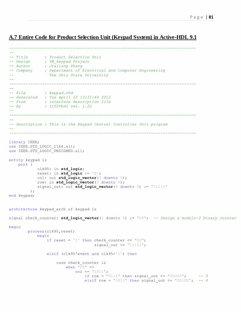
A.7 Entire Code for Product Selection Unit (Keypad System)…………81
A.8 Entire Code for Seven-Segment Display Unit (Display System)….83
A.9 Entire Code for User Interface Unit Top-Level Design……………85
A.10 Entire Code for Clock Divider Unit
(50 MHz to 95 Hz and 1.5 KHz)…………………………….…….87
A.11 Entire Code for Modified Product
Selection Unit (Keypad System)……………………………….…88
A.12 Entire Code for System Controller Unit (Control Center)…….….91
A.13 Entire Code for Improved Four-Digit
Seven-Segment Display Unit…………………………………..…96
A.14 Entire Code for Final Vending Machine Top-Level Design..……99
A.15 Pin Numbers and Configurations for
NexysTM 2 Board (File Nexys2_1200General.ucf)………….…102
A.16 User Instruction of the Designed Vending Machine………....….109
P a g e | 7
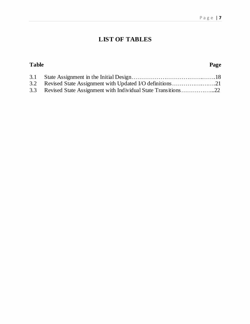
LIST OF TABLES
Table Page
3.1 State Assignment in the Initial Design……………………………….…….18 3.2 Revised State Assignment with Updated I/O definitions…………….…….21
3.3 Revised State Assignment with Individual State Transitions……………...22
P a g e | 8
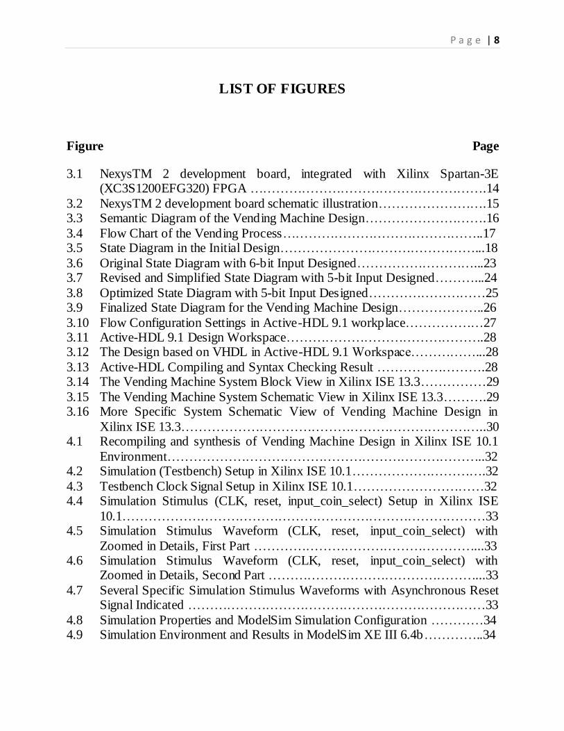
LIST OF FIGURES
Figure Page
3.1 NexysTM 2 development board, integrated with Xilinx Spartan-3E (XC3S1200EFG320) FPGA ……………………………………………….14
3.2 NexysTM 2 development board schematic illustration…………………….15 3.3 Semantic Diagram of the Vending Machine Design……………………….16
3.4 Flow Chart of the Vending Process………………………………………..17 3.5 State Diagram in the Initial Design………………………………………...18
3.6 Original State Diagram with 6-bit Input Designed………………………...23 3.7 Revised and Simplified State Diagram with 5-bit Input Designed………...24
3.8 Optimized State Diagram with 5-bit Input Designed………………………25 3.9 Finalized State Diagram for the Vending Machine Design………………..26
3.10 Flow Configuration Settings in Active-HDL 9.1 workplace………………27 3.11 Active-HDL 9.1 Design Workspace……………………………………….28 3.12 The Design based on VHDL in Active-HDL 9.1 Workspace……………...28
3.13 Active-HDL Compiling and Syntax Checking Result …………………….28 3.14 The Vending Machine System Block View in Xilinx ISE 13.3……………29
3.15 The Vending Machine System Schematic View in Xilinx ISE 13.3……….29 3.16 More Specific System Schematic View of Vending Machine Design in
Xilinx ISE 13.3……………………………………………………………..30 4.1 Recompiling and synthesis of Vending Machine Design in Xilinx ISE 10.1
Environment………………………………………………………………..32 4.2 Simulation (Testbench) Setup in Xilinx ISE 10.1………………………….32
4.3 Testbench Clock Signal Setup in Xilinx ISE 10.1…………………………32 4.4 Simulation Stimulus (CLK, reset, input_coin_select) Setup in Xilinx ISE
10.1…………………………………………………………………………33 4.5 Simulation Stimulus Waveform (CLK, reset, input_coin_select) with
Zoomed in Details, First Part ……………………………………………...33 4.6 Simulation Stimulus Waveform (CLK, reset, input_coin_select) with
Zoomed in Details, Second Part …………………………………………...33
4.7 Several Specific Simulation Stimulus Waveforms with Asynchronous Reset Signal Indicated ……………………………………………………………33
4.8 Simulation Properties and ModelSim Simulation Configuration …………34 4.9 Simulation Environment and Results in ModelSim XE III 6.4b…………..34
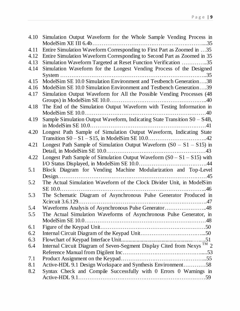
P a g e | 9
4.10 Simulation Output Waveform for the Whole Sample Vending Process in ModelSim XE III 6.4b……………………………………………………...35
4.11 Entire Simulation Waveform Corresponding to First Part as Zoomed in …35 4.12 Entire Simulation Waveform Corresponding to Second Part as Zoomed in 35
4.13 Simulation Waveform Targeted at Reset Function Verification …………..35 4.14 Simulation Waveform for the Longest Vending Process of the Designed
System ……………………………………………………………………..35 4.15 ModelSim SE 10.0 Simulation Environment and Testbench Generation….38 4.16 ModelSim SE 10.0 Simulation Environment and Testbench Generation….39
4.17 Simulation Output Waveform for All the Possible Vending Processes (48 Groups) in ModelSim SE 10.0……………………………………………..40
4.18 The End of the Simulation Output Waveform with Testing Information in ModelSim SE 10.0…………………………………………………………40
4.19 Sample Simulation Output Waveform, Indicating State Transition S0 – S4B, in ModelSim SE 10.0………………………………………………………41
4.20 Longest Path Sample of Simulation Output Waveform, Indicating State Transition S0 – S1 – S15, in ModelSim SE 10.0…………………………..42
4.21 Longest Path Sample of Simulation Output Waveform (S0 – S1 – S15) in Detail, in ModelSim SE 10.0………………………………………………43
4.22 Longest Path Sample of Simulation Output Waveform (S0 – S1 – S15) with I/O Status Displayed, in ModelSim SE 10.0……………………………….44
5.1 Block Diagram for Vending Machine Modularization and Top-Level
Design………………………………………………………………………45 5.2 The Actual Simulation Waveform of the Clock Divider Unit, in ModelSim
SE 10.0……………………………………………………………………..46 5.3 The Schematic Diagram of Asynchronous Pulse Generator Produced in
Xcircuit 3.6.129…………………………………………………………….47 5.4 Waveforms Analysis of Asynchronous Pulse Generator…………………..48
5.5 The Actual Simulation Waveforms of Asynchronous Pulse Generator, in ModelSim SE 10.0…………………………………………………………48
6.1 Figure of the Keypad Unit…………………………………………………50 6.2 Internal Circuit Diagram of the Keypad Unit……………………………...50
6.3 Flowchart of Keypad Interface Unit....................................................….....51 6.4 Internal Circuit Diagram of Seven-Segment Display Cited from Nexys
TM 2
Reference Manual from Digilent Inc…………………………………….....53 7.1 Product Assignment on the Keypad………………………………………..55 8.1 Active-HDL 9.1 Design Workspace and Synthesis Environment…………58
8.2 Syntax Check and Compile Successfully with 0 Errors 0 Warnings in Active-HDL 9.1……………………………………………………………59
P a g e | 10
8.3 Synthesis Option in Active-HDL 9.1………………………………………59 8.4 Xilinx XST Synthesis Result: Successful without Warning(s) in Active-HDL
9.1…………………………………………………………………………..60 9.1 Active-HDL 9.1 Design Workspace and Implementation Environment…..61
9.2 Implementation Options Configuration Window in Active-HDL 9.1……..61 9.3 Implementation Result in Active-HDL 9.1………………………………...62
10.1 Project Development Tools and Environment………………………….….63 10.2 Keypad User Interface System Setup in Detail…………………………….64 10.3 Adept 2.9.4 FPGA Program Tool Wizard………………………………….64
P a g e | 11
CHAPTER 1
Introduction
In recent years, with the rapid development of Integrated Circuit technology, particularly
the fast growth of FPGA (Field Programmable Gate Array) devices, electrical engineers could
design and produce more and more types of electronic devices, and fulfill almost all kinds of
needs in modern society.
Design with FPGA technology is majorly based on computer or CAD (Computer Aided
Design) tools, in order to accomplish the logic synthesis, placing, routing and simulation
procedures etc. for the whole digital system.
One of the important methods to develop FPGA devices based on CAD tools is the
Hardware Description Language (HDL), which is programmed to describe the logic elements
and the functions or even the behaviors of system hardware. VHDL (Very High Speed Integrated
Circuit Hardware Description Language) is one of the common Hardware Description Language,
which will also be used in this research project to design vending machines.
P a g e | 12
CHAPTER 2
Design Proposal
Vending Machine Design Specifications
The coins that can be received are in 3 types:
Dime (¢10), Quarter (¢25), Dollar ($1)
Note: there is a slight change from the coins available in the previous specifications. The designer replaced one Half Dollar (¢50) coin with one Dollar ($1) coin, because comparing to a Half Dollar coin, one Dollar coin is more popular nowadays, and people still use one Dollar
coins in daily life.
The number of products available to purchase:
As many as 16 different products, numbering in Hexadecimal values, namely Prod#0, Prod#1, Prod#2 …, Prod#A representing Product No. 10, Prod#B representing Product No. 11,
…, Prod#E representing Product No. 14, and Prod#F representing Product No. 15.
The prices of each product:
Three different prices are assigned for each product: $1.00, $1.25 and $1.50 respectively. And the vending machine will not give changes to customers as the initial design specification.
Additional functions:
There will be a LED display component interacting with users in the vending process, showing the total value of coins received and then, the product number the user select during vending process.
Project procedure:
Use Xilinx ISE Suite and other CAD tools to design the internal digital circuit and system of the Vending Machines, include block diagram, whole system printout and debugging. And the final user instruction will be offered.
P a g e | 13
CHAPTER 3
System Controller Unit Design (Control Center)
3.1 Component Details
The author chooses the most updated ISE Design Suite 13.3 by Xilinx, Inc., combining
with Active-HDL 9.1 Student Edition by Aldec, Inc. as the develop software and CAD tools, and
Adept 2.9.4 by Digilent Inc. as the FPGA programming tool. The very first step of the project is
to complete program design, synthesis and timing simulations on the computer and ISE design
environment. And then, to generate executive file and to program FPGA will physically verify
the whole design.
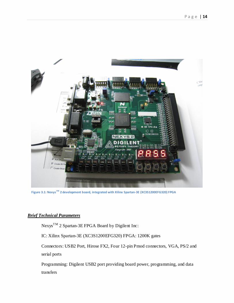
One of the major components in this Vending Machine design is the FPGA device. The
designer chooses XC3S1200E-FG320 FPGA, which belongs to Xilinx Spartan-3E FPGA
Family. And the reason for this choice is that this type of FPGA is very capable and powerful for
a small scale design and research, yet its price is very reasonable. According to the Xilinx
Website, for one piece of XC3S1200E, the price is approximately between $60.75 and $69.83.
Furthermore, there is a good development board for Spartan-3E FPGA that the author purchased
and worked with, which is NexysTM 2 by Digilent Inc., as is shown in the following figure. So
this type of FPGA and development kits are very suitable and popular for starting learner, and
they will make the whole vending machine design project more practical and economical.
P a g e | 14
Brief Technical Parameters
NexysTM 2 Spartan-3E FPGA Board by Digilent Inc:
IC: Xilinx Spartan-3E (XC3S1200EFG320) FPGA: 1200K gates
Connectors: USB2 Port, Hirose FX2, Four 12-pin Pmod connectors, VGA, PS/2 and
serial ports
Programming: Digilent USB2 port providing board power, programming, and data
transfers
Figure 3.1: NexysTM 2 development board, integrated with Xilinx Spartan-3E (XC3S1200EFG320) FPGA
P a g e | 15
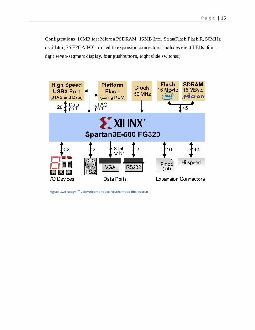
Configurations: 16MB fast Micron PSDRAM, 16MB Intel StrataFlash Flash R, 50MHz
oscillator, 75 FPGA I/O’s routed to expansion connectors (includes eight LEDs, four-
digit seven-segment display, four pushbuttons, eight slide switches)
Figure 3.2: NexysTM 2 development board schematic illustration
P a g e | 16
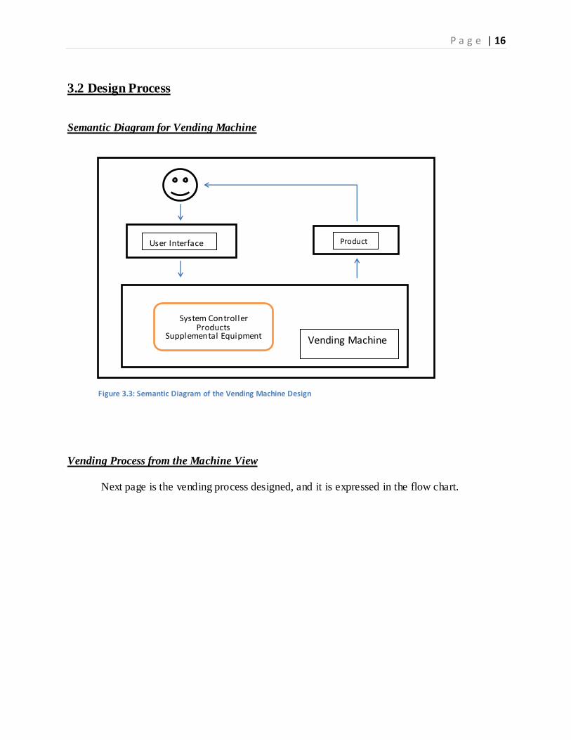
Vending Machine
User Interface Product
3.2 Design Process
Semantic Diagram for Vending Machine
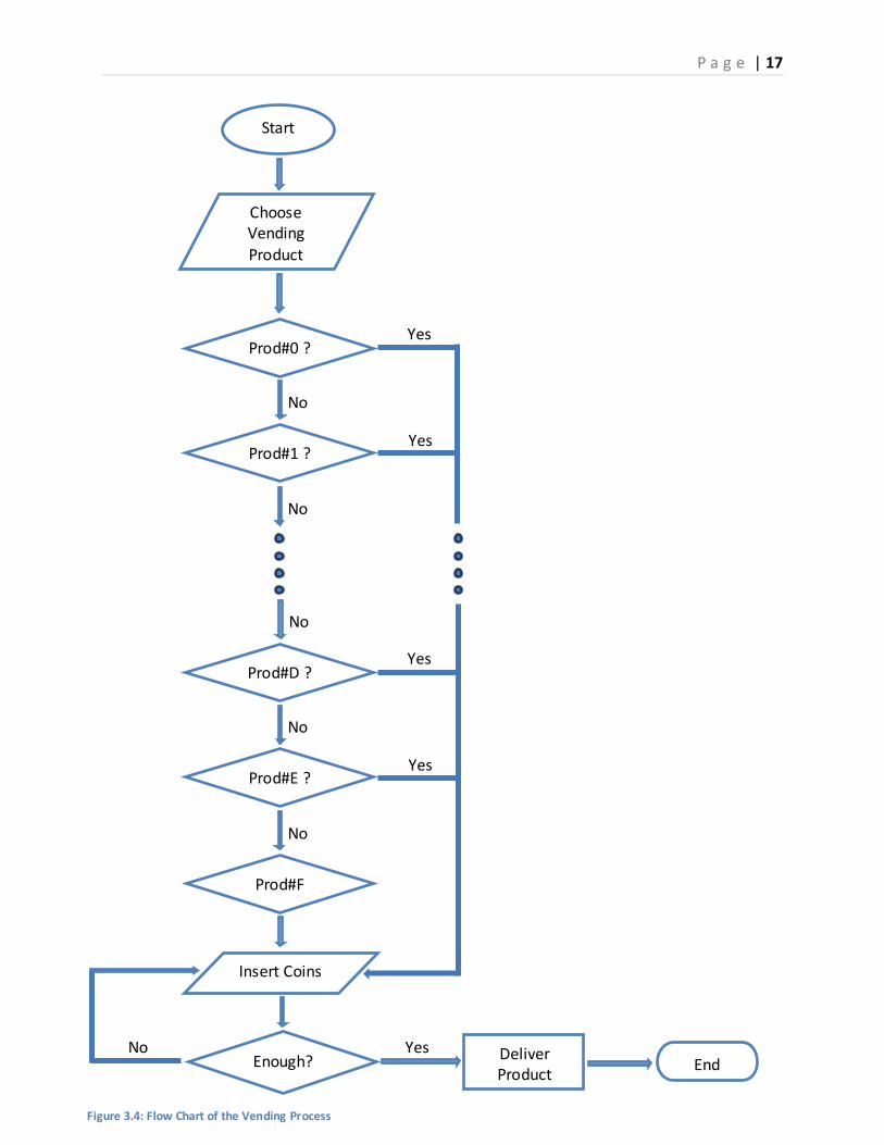
Vending Process from the Machine View
Next page is the vending process designed, and it is expressed in the flow chart.
System Controller Products
Supplemental Equipment
Figure 3.3: Semantic Diagram of the Vending Machine Design
P a g e | 17
Yes No
No
Start
Choose Vending
Product
Prod#0 ?
Prod#1 ?
No
Yes
Yes
No
Prod#F
Insert Coins
Enough? Deliver Product
End
Prod#D ?
Prod#E ?
No
Yes
No
Yes
Figure 3.4: Flow Chart of the Vending Process
P a g e | 18
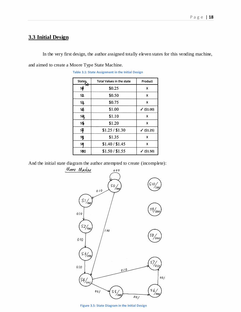
Table 3.1: State Assignment in the Initial Design
3.3 Initial Design
In the very first design, the author assigned totally eleven states for this vending machine,
and aimed to create a Moore Type State Machine.
And the initial state diagram the author attempted to create (incomplete):
Figure 3.5: State Diagram in the Initial Design
P a g e | 19
But soon, the designer realized that it is almost impossible to implement so many
functions of the vending machine by such few states. Also, the design variables – specifically the
number of bits for the state machine inputs are not enough. Then, it follows with the further
modified design, beginning with a clearly defined Input and Output I/O definitions:
3.4 I/O Design Definitions
i) Input signal:
“input_coin_select” is the input signal, measuring and symbolizing different coins
inserted each time and product selected by the customer through the vending process.
Set “input_coin_select” as a vector of size 5 (4 downto 0): the MSB, i.e.
input_coin_select(4), represents receiving one Dollar coin ($1), input_coin_select (3) represents
receiving one Quarter coin(¢25), and input_coin_select (2) represents receiving one Dime(¢10),
those bits are reserved for measuring coins inserting each time.
On the other hand, input_coin_select (1), with asserting to 1, means the customer selected
the product of price ($1.25), input_coin_select (0), with asserting to 1, means the customer
selected the product of price ($1.00), those bits are reserved for indicating the selection from the
customer and are used to make the decision whether to deliver the corresponding product to the
customer at the end of the vending process. Since if the selection was neither the product of price
($1.25) nor the product of price ($1.00), then it must be the product of price ($1.50) eventually,
so this design reduces from six- input mode to five- input mode for the state machine, saving one
P a g e | 20
bit for the “input_coin_select” input signal. And to some degree, this one bit saving can reduce
the complexity and manufacturing cost of the designed vending machine.
And if the value of each individual “input_coin_select (4 downto 2)” bit is 1, it means
one corresponding coin was received; if the value of each bit remains as 0, it means there is no
corresponding coin inserted currently.
ii) Output signal:
The output signal is named as “output_product”, and is set as a vector with dimension of
3 (2 downto 0): output_product (2) is reserved for signaling the delivery of the ($1.50) vending
product to the customer, output_product (1) is reserved for signaling the delivery of the ($1.25)
vending product to the customer, and output_product (0) is reserved for signaling the delivery of
the ($1.00) vending product to the customer.
If each individual bit of “output_product” is 1, then there will be a certain product
delivered to the customer; if the single bit of “output_product” is 0, then there will be no action
inside the vending machine.
P a g e | 21
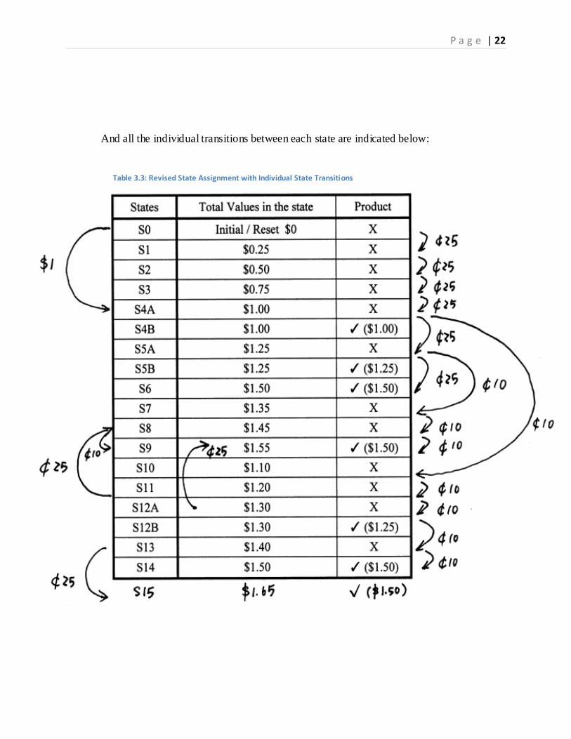
3.5 Revised Design
Based on the I/O definitions, below is the revised state assignment and corresponding table.
States Total Values in the state Product
S0 Initial / Reset $0 X
S1 $0.25 X
S2 $0.50 X
S3 $0.75 X
S4A $1.00 X
S4B $1.00 ✓ ($1.00)
S5A $1.25 X
S5B $1.25 ✓ ($1.25)
S6 $1.50 ✓ ($1.50)
S7 $1.35 X
S8 $1.45 X
S9 $1.55 ✓ ($1.50)
S10 $1.10 X
S11 $1.20 X
S12A $1.30 X
S12B $1.30 ✓ ($1.25)
S13 $1.40 X
S14 $1.50 ✓ ($1.50)
S15 $1.65 ✓ ($1.50)
Table 3.2: Revised State Assignment with Updated I/O definitions
P a g e | 22
And all the individual transitions between each state are indicated below:
Table 3.3: Revised State Assignment with Individual State Transitions
P a g e | 23
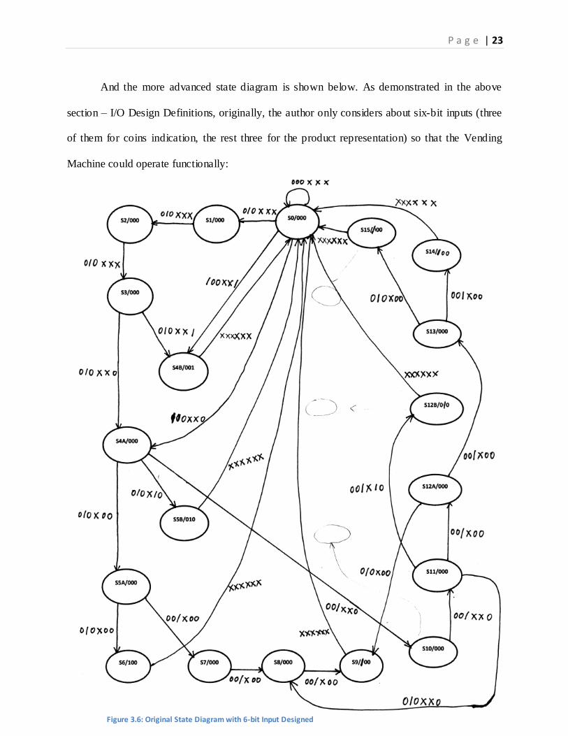
And the more advanced state diagram is shown below. As demonstrated in the above
section – I/O Design Definitions, originally, the author only considers about six-bit inputs (three
of them for coins indication, the rest three for the product representation) so that the Vending
Machine could operate functionally:
Figure 3.6: Original State Diagram with 6-bit Input Designed
P a g e | 24
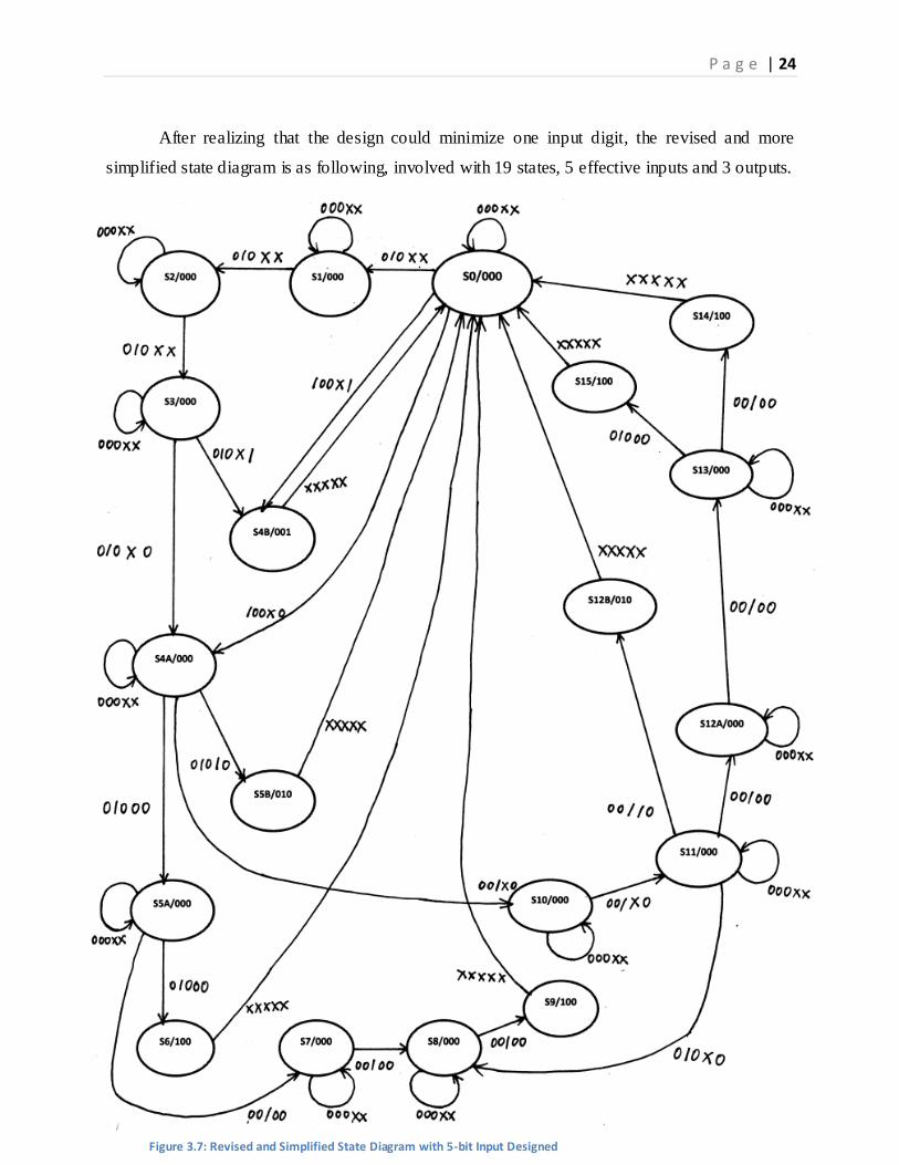
After realizing that the design could minimize one input digit, the revised and more
simplified state diagram is as following, involved with 19 states, 5 effective inputs and 3 outputs.
Figure 3.7: Revised and Simplified State Diagram with 5-bit Input Designed
P a g e | 25
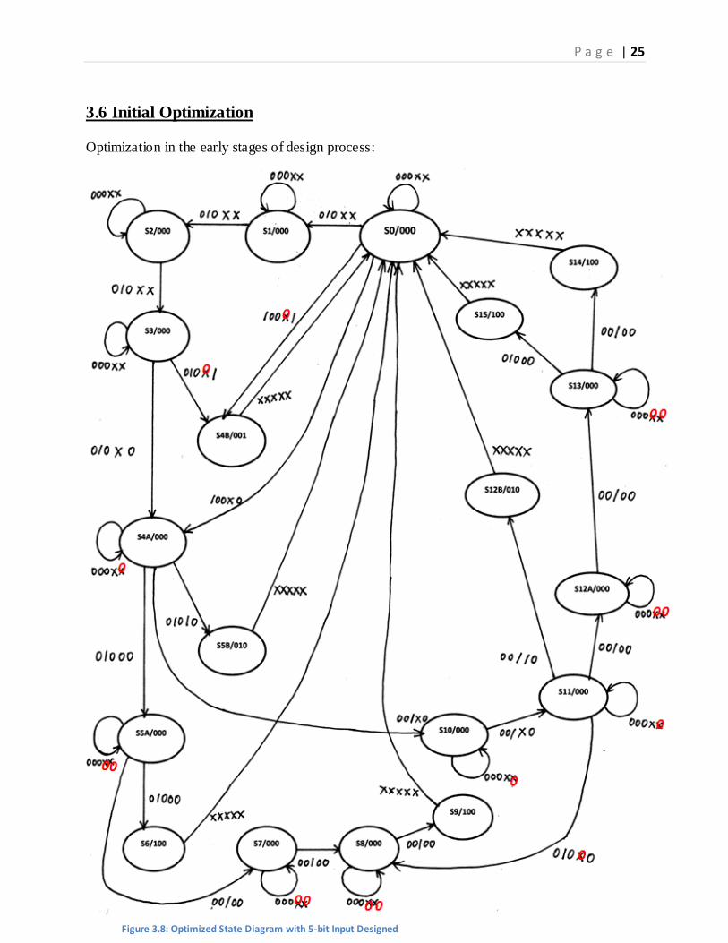
3.6 Initial Optimization
Optimization in the early stages of design process:
Figure 3.8: Optimized State Diagram with 5-bit Input Designed
P a g e | 26
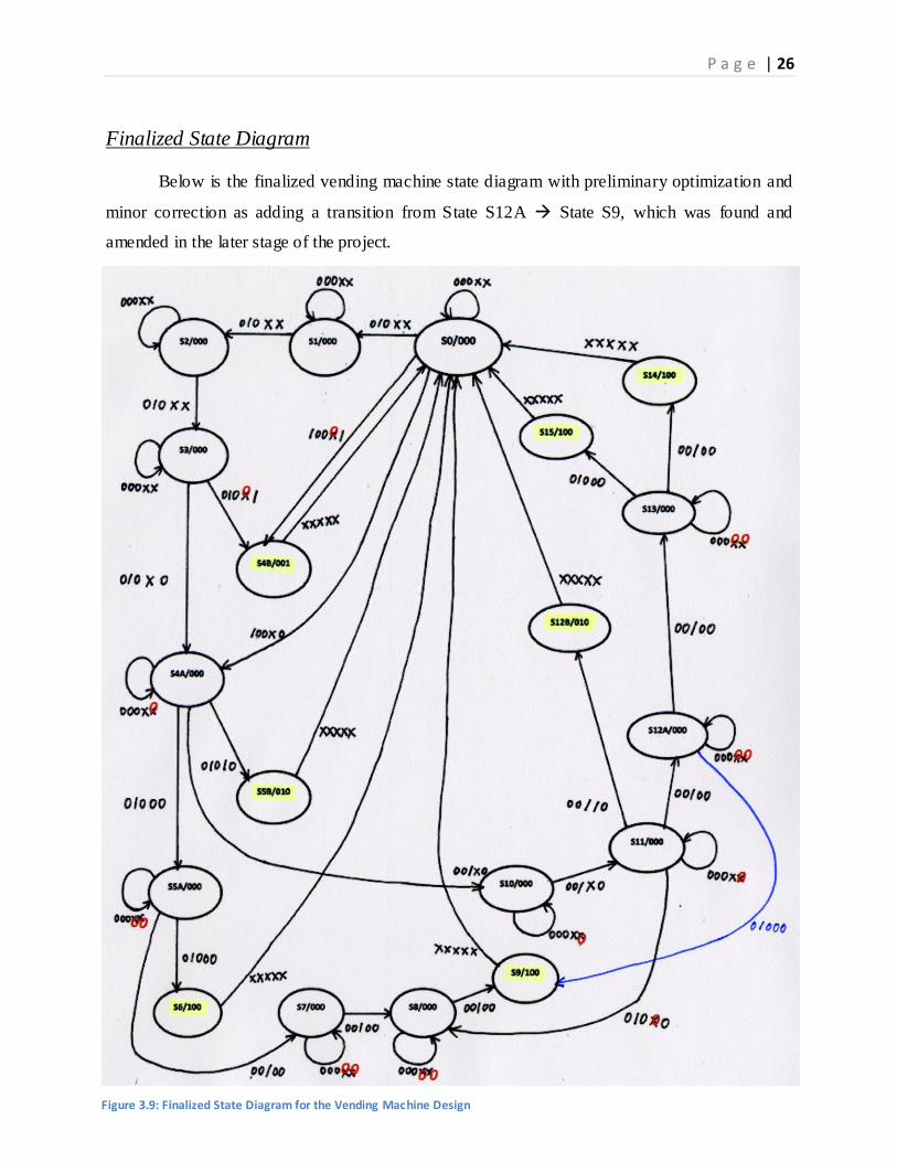
Finalized State Diagram
Below is the finalized vending machine state diagram with preliminary optimization and
minor correction as adding a transition from State S12A State S9, which was found and
amended in the later stage of the project.
Figure 3.9: Finalized State Diagram for the Vending Machine Design
P a g e | 27
Instead of assigning several “don’t cares” as input stimulus, the designer optimized those
bits with a forced ‘0’ assignment. That is because in some scenarios, it is certain that the
customer has made the product choice explicitly, so the rest options (product choices) should
always be eliminated, meaning to be assigned with ‘0’ automatically. And this will considerably
save some gates and resources on FPGA programming.
3.7 Machine Design with VHDL
As is demonstrated before, with the new NexysTM 2 Spartan-3E development board by
Digilent Inc. to implement the design, the author changed from Xilinx ISE to the CAD tool
Active-HDL by Aldec Inc. and used it as the main design tool. However, Active-HDL 9.1 does
need to call the library of Xilinx Spartan-3E FPGA family when compiling and synthesizing the
design. The following is the brief design setups:
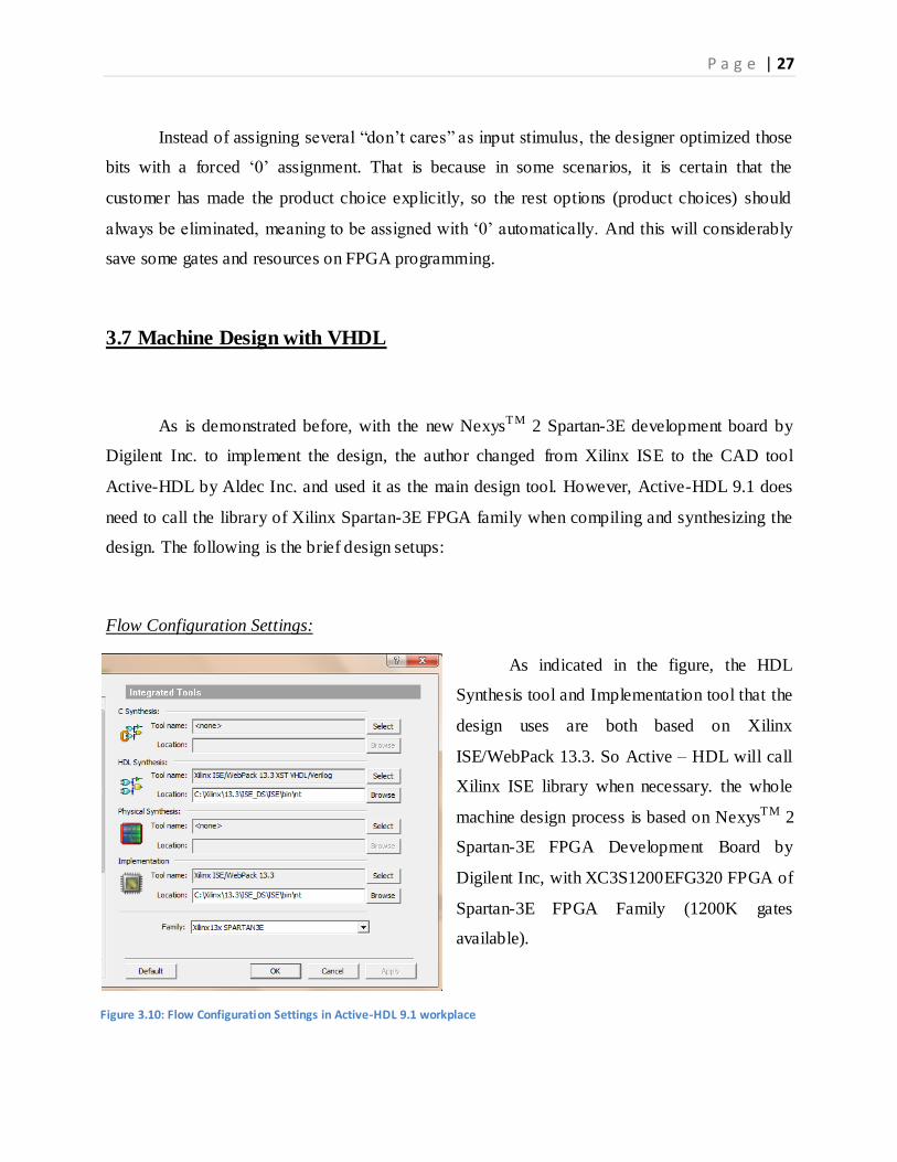
Flow Configuration Settings:
As indicated in the figure, the HDL
Synthesis tool and Implementation tool that the
design uses are both based on Xilinx
ISE/WebPack 13.3. So Active – HDL will call
Xilinx ISE library when necessary. the whole
machine design process is based on NexysTM 2
Spartan-3E FPGA Development Board by
Digilent Inc, with XC3S1200EFG320 FPGA of
Spartan-3E FPGA Family (1200K gates
available).
Figure 3.10: Flow Configuration Settings in Active-HDL 9.1 workplace
P a g e | 28
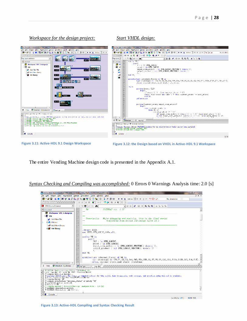
Workspace for the design project: Start VHDL design:
The entire Vending Machine design code is presented in the Appendix A.1.
Syntax Checking and Compiling was accomplished: 0 Errors 0 Warnings Analysis time: 2.0 [s]
Figure 3.11: Active-HDL 9.1 Design Workspace Figure 3.12: the Design based on VHDL in Active-HDL 9.1 Workspace
Figure 3.13: Active-HDL Compiling and Syntax Checking Result
P a g e | 29
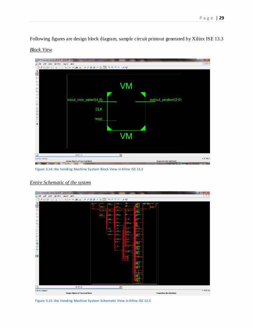
Following figures are design block diagram, sample circuit printout generated by Xilinx ISE 13.3
Block View
Entire Schematic of the system
Figure 3.14: the Vending Machine System Block View in Xilinx ISE 13.3
Figure 3.15: the Vending Machine System Schematic View in Xilinx ISE 13.3
P a g e | 30
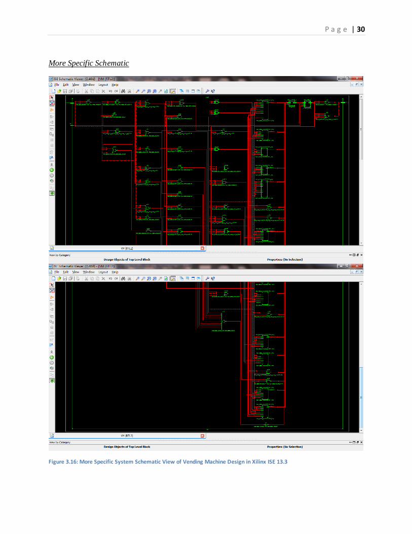
More Specific Schematic
Figure 3.16: More Specific System Schematic View of Vending Machine Design in Xilinx ISE 13.3
P a g e | 31
CHAPTER 4
System Controller Simulation and Verification
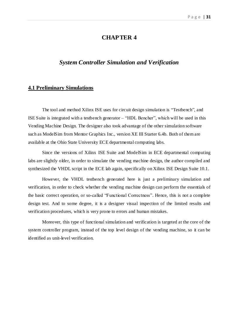
4.1 Preliminary Simulations
The tool and method Xilinx ISE uses for circuit design simulation is “Testbench”, and
ISE Suite is integrated with a testbench generator – “HDL Bencher”, which will be used in this
Vending Machine Design. The designer also took advantage of the other simulation software
such as ModelSim from Mentor Graphics Inc., version XE III Starter 6.4b. Both of them are
available at the Ohio State University ECE departmental computing labs.
Since the versions of Xilinx ISE Suite and ModelSim in ECE departmental computing
labs are slightly older, in order to simulate the vending machine design, the author compiled and
synthesized the VHDL script in the ECE lab again, specifically on Xilinx ISE Design Suite 10.1.
However, the VHDL testbench generated here is just a preliminary simulation and
verification, in order to check whether the vending machine design can perform the essentials of
the basic correct operation, or so-called “Functional Correctness”. Hence, this is not a complete
design test. And to some degree, it is a designer visual inspection of the limited results and
verification procedures, which is very prone to errors and human mistakes.
Moreover, this type of functional simulation and verification is targeted at the core of the
system controller program, instead of the top level design of the vending machine, so it can be
identified as unit-level verification.
P a g e | 32
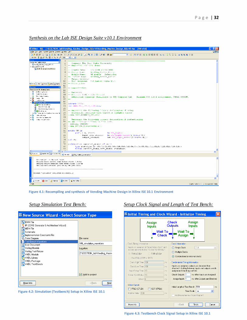
Synthesis on the Lab ISE Design Suite v10.1 Environment
Setup Simulation Test Bench: Setup Clock Signal and Length of Test Bench:
Figure 4.1: Recompiling and synthesis of Vending Machine Design in Xilinx ISE 10.1 Environment
Figure 4.2: Simulation (Testbench) Setup in Xilinx ISE 10.1
Figure 4.3: Testbench Clock Signal Setup in Xilinx ISE 10.1
P a g e | 33
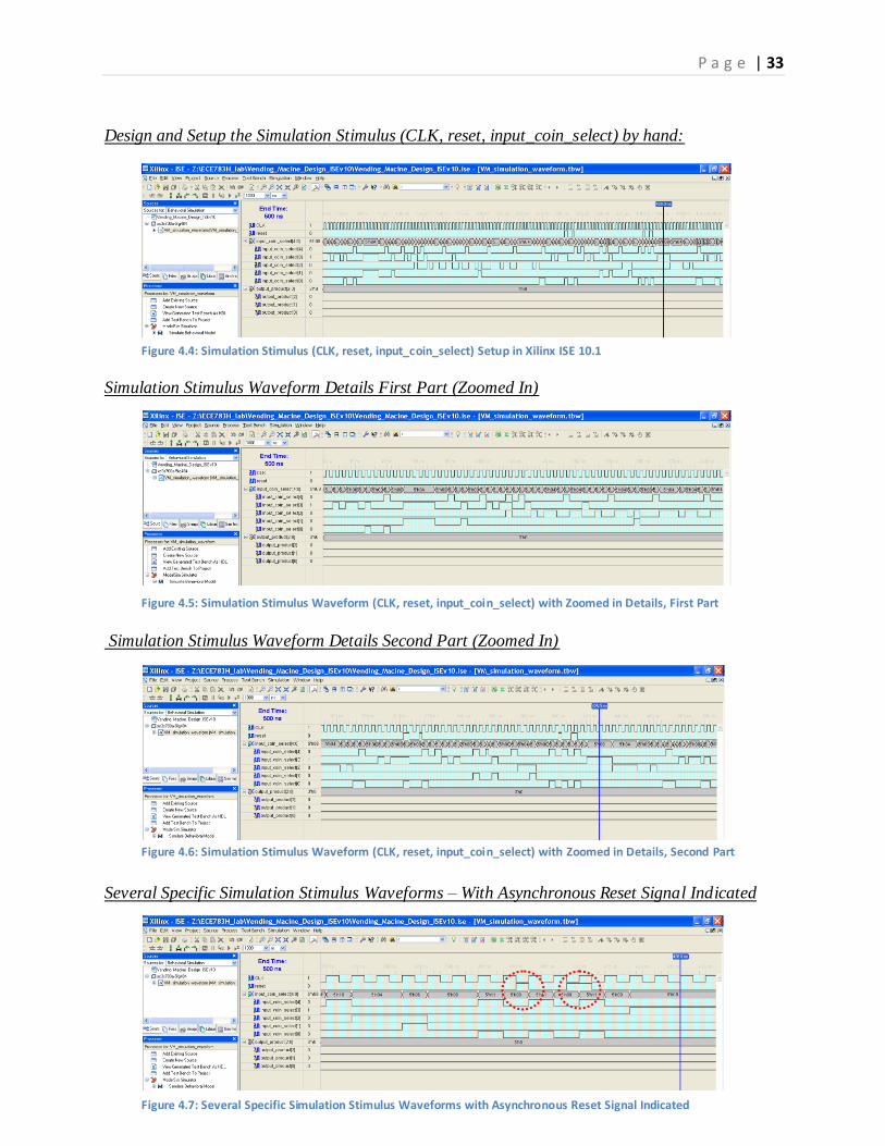
Design and Setup the Simulation Stimulus (CLK, reset, input_coin_select) by hand:
Simulation Stimulus Waveform Details First Part (Zoomed In)
Simulation Stimulus Waveform Details Second Part (Zoomed In)
Several Specific Simulation Stimulus Waveforms – With Asynchronous Reset Signal Indicated
Figure 4.4: Simulation Stimulus (CLK, reset, input_coin_select) Setup in Xilinx ISE 10.1
Figure 4.5: Simulation Stimulus Waveform (CLK, reset, input_coin_select) with Zoomed in Details, First Part
Figure 4.6: Simulation Stimulus Waveform (CLK, reset, input_coin_select) with Zoomed in Details, Second Part
Figure 4.7: Several Specific Simulation Stimulus Waveforms with Asynchronous Reset Signal Indicated
P a g e | 34
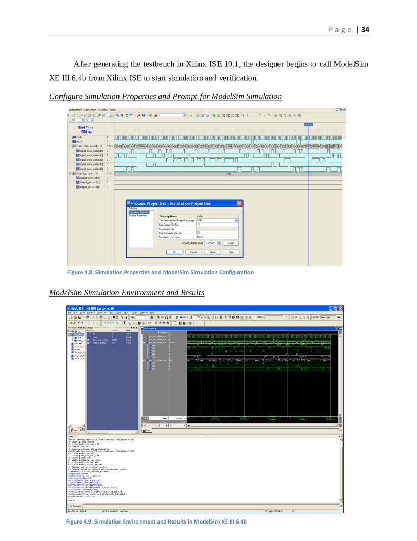
After generating the testbench in Xilinx ISE 10.1, the designer begins to call ModelSim
XE III 6.4b from Xilinx ISE to start simulation and verification.
Configure Simulation Properties and Prompt for ModelSim Simulation
ModelSim Simulation Environment and Results
Figure 4.8: Simulation Properties and ModelSim Simulation Configuration
Figure 4.9: Simulation Environment and Results in ModelSim XE III 6.4b
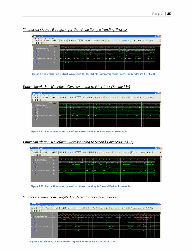
P a g e | 35
Simulation Output Waveform for the Whole Sample Vending Process
Entire Simulation Waveform Corresponding to First Part (Zoomed In)
Entire Simulation Waveform Corresponding to Second Part (Zoomed In)
Simulation Waveform Targeted at Reset Function Verification
Figure 4.10: Simulation Output Waveform for the Whole Sample Vending Process in ModelSim XE III 6.4b
Figure 4.11: Entire Simulation Waveform Corresponding to First Part as Zoomed in
Figure 4.12: Entire Simulation Waveform Corresponding to Second Part as Zoomed in
Figure 4.13: Simulation Waveform Targeted at Reset Function Verification
P a g e | 36
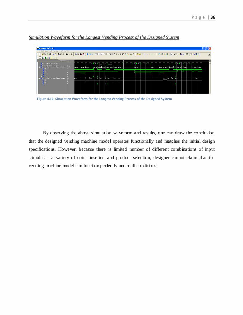
Simulation Waveform for the Longest Vending Process of the Designed System
By observing the above simulation waveform and results, one can draw the conclusion
that the designed vending machine model operates functionally and matches the initial design
specifications. However, because there is limited number of different combinations of input
stimulus – a variety of coins inserted and product selection, designer cannot claim that the
vending machine model can function perfectly under all conditions.
Figure 4.14: Simulation Waveform for the Longest Vending Process of the Designed System
P a g e | 37
4.2 Complete Simulation and Verification
The visual inspection and limited testing cannot satisfy the project needs, so the author
designs a complete simulation and verification suite furthermore, and performs the “exhausted
simulation and verification” to check the design functionality. The idea of this approach is to
check the response of the design model, given the mechanism that the testing procedure will
automate the output using waveforms from CAD for verification. In the complete test, the testing
object must insure that with all possible input combinations, it will produce the expected output.
What is more, this new testbench and verification suite involves with the TEXT IO procedures
and functions, which is located in the library STD – TEXT IO package. And nowadays, it
requires comparatively more time and effort to direct a complete and successful simulation and
verification of a design project than to accomplish the design initially.
Theoretically, the approach of this complete functional simulation and verification is
White Box Verification. And it targets to the top level design of the vending machine model,
rather than the core of the system controller program as tested in Section 4.1. The details of the
top level design will be discussed in Chapter 5 – Peripheral Component Design below. In this
new approach of simulation and verification, the final waveforms will log various significant
internal signals and timing managements. And most importantly, it can monitor the whole
process and internal state transitions of the state machine during the testing procedure.
In this testing procedure, the designer begins to use ModelSim SE 10.0 from Mentor
Graphics Inc. And the new testbench is generated as below in ModelSim. The purpose of this
new testbench is to apply stimulus signals to the design model and observe the response of the
design model to those signals, whereas, it is all automated during the testing procedure.
The outside file contains both the input stimulus and the expected response, and it is easy
to modify them without affecting the system controller and testbench design.
P a g e | 38
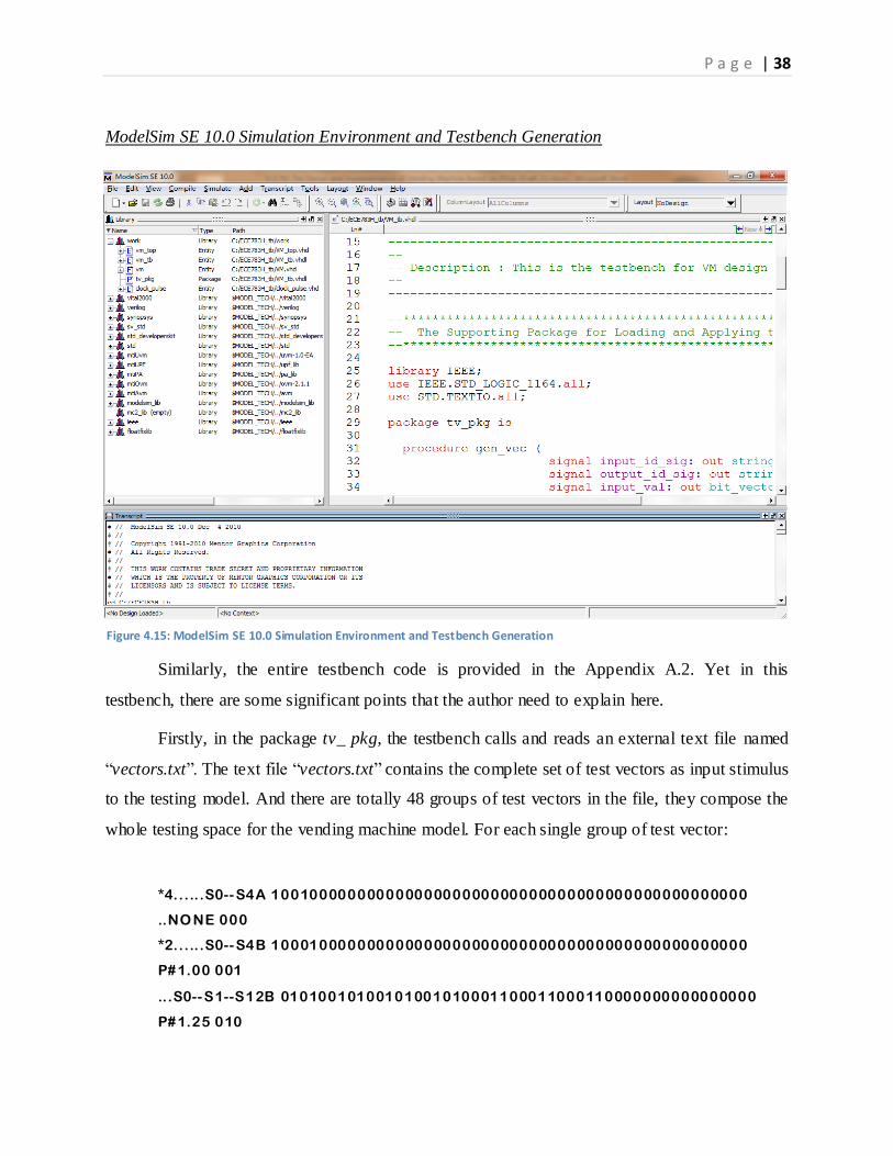
ModelSim SE 10.0 Simulation Environment and Testbench Generation
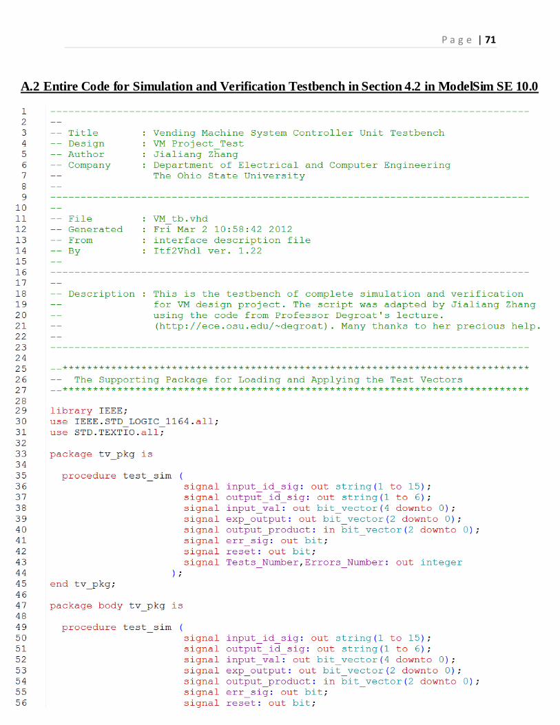
Similarly, the entire testbench code is provided in the Appendix A.2. Yet in this
testbench, there are some significant points that the author need to explain here.
Firstly, in the package tv_ pkg, the testbench calls and reads an external text file named
“vectors.txt”. The text file “vectors.txt” contains the complete set of test vectors as input stimulus
to the testing model. And there are totally 48 groups of test vectors in the file, they compose the
whole testing space for the vending machine model. For each single group of test vector:
*4......S0-- S4A 10010000000000000000000000000000000000000000000000
..NO NE 000
*2......S0-- S4B 10001000000000000000000000000000000000000000000000
P# 1.00 001
...S0-- S1--S12B 01010010100101001010001100011000110000000000000000
P# 1.25 010
Figure 4.15: ModelSim SE 10.0 Simulation Environment and Testbench Generation
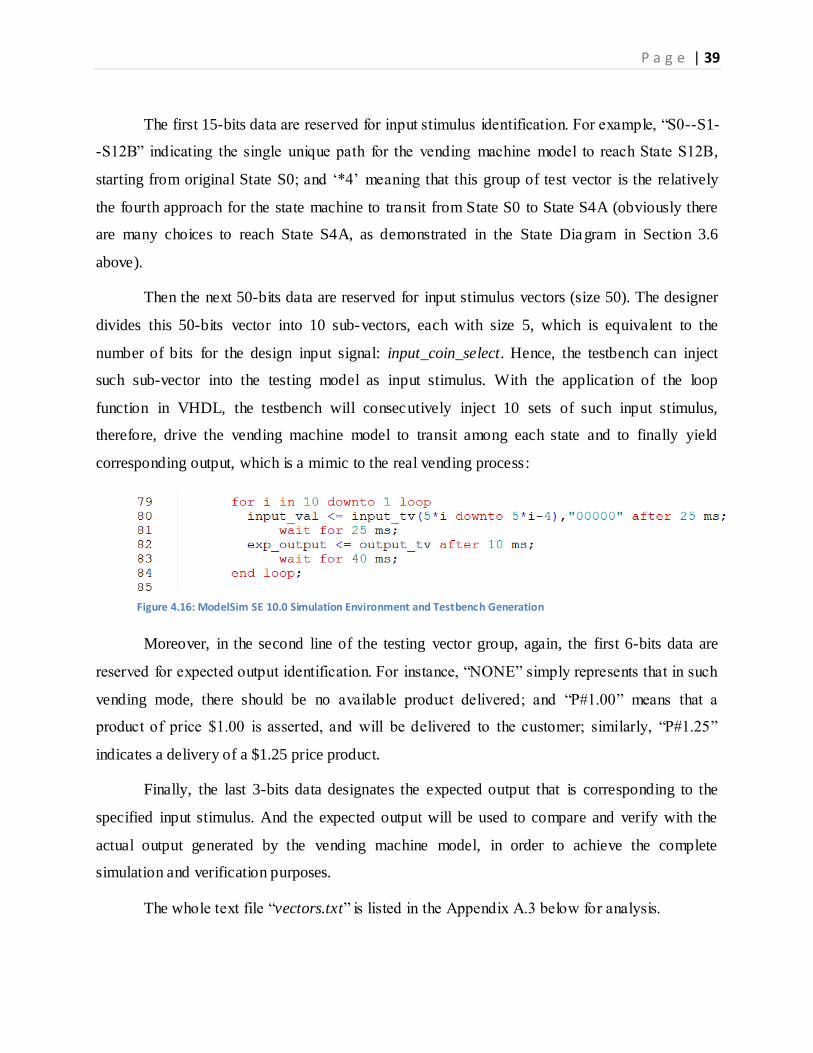
P a g e | 39
The first 15-bits data are reserved for input stimulus identification. For example, “S0--S1-
-S12B” indicating the single unique path for the vending machine model to reach State S12B,
starting from original State S0; and ‘*4’ meaning that this group of test vector is the relatively
the fourth approach for the state machine to transit from State S0 to State S4A (obviously there
are many choices to reach State S4A, as demonstrated in the State Diagram in Section 3.6
above).
Then the next 50-bits data are reserved for input stimulus vectors (size 50). The designer
divides this 50-bits vector into 10 sub-vectors, each with size 5, which is equivalent to the
number of bits for the design input signal: input_coin_select. Hence, the testbench can inject
such sub-vector into the testing model as input stimulus. With the application of the loop
function in VHDL, the testbench will consecutively inject 10 sets of such input stimulus,
therefore, drive the vending machine model to transit among each state and to finally yield
corresponding output, which is a mimic to the real vending process:
Moreover, in the second line of the testing vector group, again, the first 6-bits data are
reserved for expected output identification. For instance, “NONE” simply represents that in such
vending mode, there should be no available product delivered; and “P#1.00” means that a
product of price $1.00 is asserted, and will be delivered to the customer; similarly, “P#1.25”
indicates a delivery of a $1.25 price product.
Finally, the last 3-bits data designates the expected output that is corresponding to the
specified input stimulus. And the expected output will be used to compare and verify with the
actual output generated by the vending machine model, in order to achieve the complete
simulation and verification purposes.
The whole text file “vectors.txt” is listed in the Appendix A.3 below for analysis.
Figure 4.16: ModelSim SE 10.0 Simulation Environment and Testbench Generation
P a g e | 40
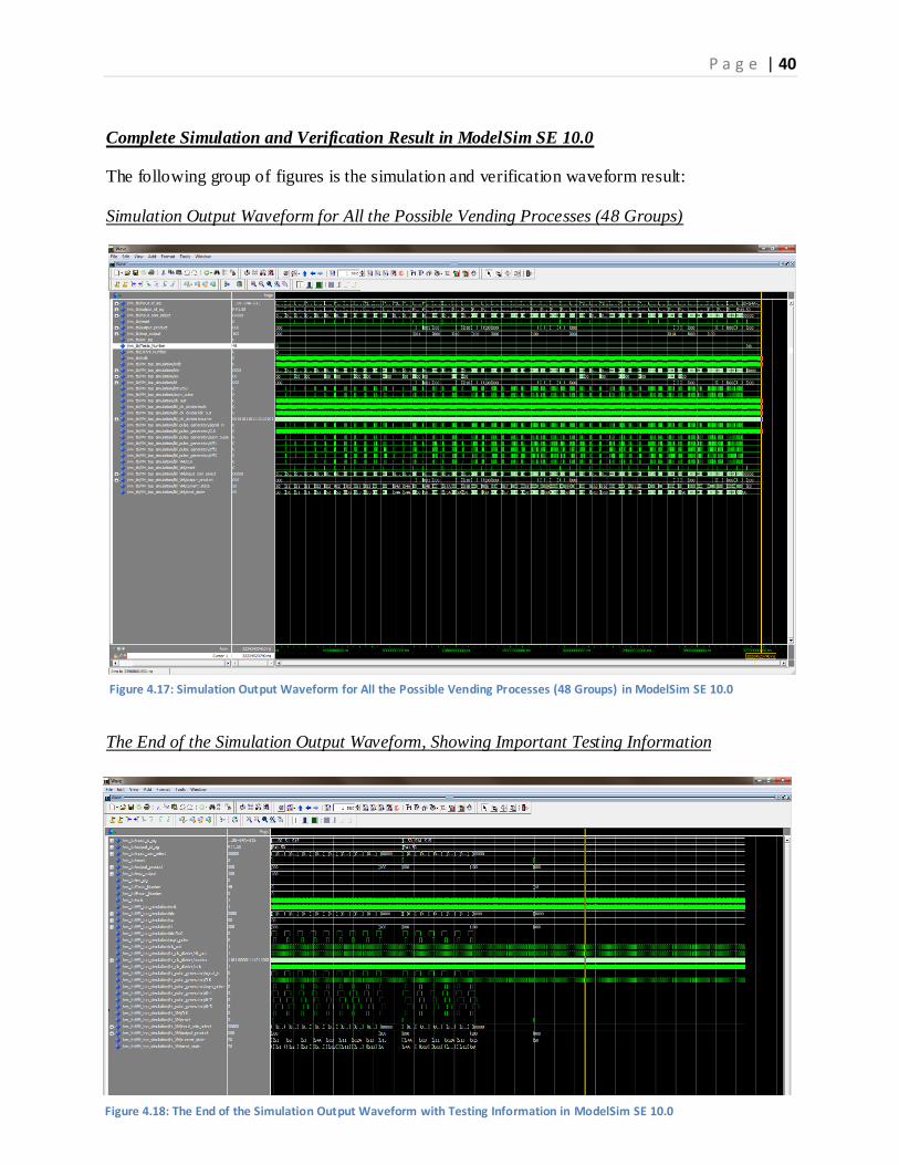
Complete Simulation and Verification Result in ModelSim SE 10.0
The following group of figures is the simulation and verification waveform result:
Simulation Output Waveform for All the Possible Vending Processes (48 Groups)
The End of the Simulation Output Waveform, Showing Important Testing Information
Figure 4.17: Simulation Output Waveform for All the Possible Vending Processes (48 Groups) in ModelSim SE 10.0
Figure 4.18: The End of the Simulation Output Waveform with Testing Information in ModelSim SE 10.0
P a g e | 41
As you can see from Figure 34 above, the waveform signal /vm_tb/Tests_Numbers is
“48”, meaning there are 48 different groups of test vectors being injected into the design model.
On the other hand, waveform signal /vm_tb/Tests_Numbers is “0”, meaning there is no error
through the whole simulation and testing process. Likewise, /vm_tb/err_sig which remains at low
level as “0” proves that there is no error founded.
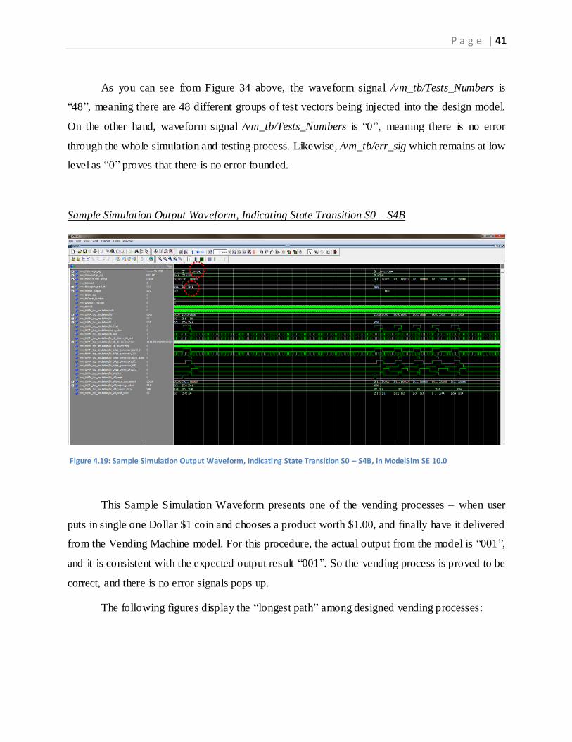
Sample Simulation Output Waveform, Indicating State Transition S0 – S4B
This Sample Simulation Waveform presents one of the vending processes – when user
puts in single one Dollar $1 coin and chooses a product worth $1.00, and finally have it delivered
from the Vending Machine model. For this procedure, the actual output from the model is “001”,
and it is consistent with the expected output result “001”. So the vending process is proved to be
correct, and there is no error signals pops up.
The following figures display the “longest path” among designed vending processes:
Figure 4.19: Sample Simulation Output Waveform, Indicating State Transition S0 – S4B, in ModelSim SE 10.0
P a g e | 42
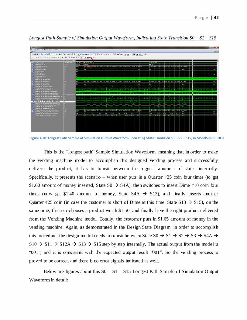
Longest Path Sample of Simulation Output Waveform, Indicating State Transition S0 – S1 – S15
This is the “longest path” Sample Simulation Waveform, meaning that in order to make
the vending machine model to accomplish this designed vending process and successfully
delivers the product, it has to transit between the biggest amounts of states internally.
Specifically, it presents the scenario – when user puts in a Quarter ¢25 coin four times (to get
$1.00 amount of money inserted, State S0 S4A), then switches to insert Dime ¢10 coin four
times (now get $1.40 amount of money, State S4A S13), and finally inserts another
Quarter ¢25 coin (in case the customer is short of Dime at this time, State S13 S15), on the
same time, the user chooses a product worth $1.50, and finally have the right product delivered
from the Vending Machine model. Totally, the customer puts in $1.65 amount of money in the
vending machine. Again, as demonstrated in the Design State Diagram, in order to accomplish
this procedure, the design model needs to transit between State S0 S1 S2 S3 S4A
S10 S11 S12A S13 S15 step by step internally. The actual output from the model is
“001”, and it is consistent with the expected output result “001”. So the vending process is
proved to be correct, and there is no error signals indicated as well.
Below are figures about this S0 – S1 – S15 Longest Path Sample of Simulation Output
Waveform in detail:
Figure 4.20: Longest Path Sample of Simulation Output Waveform, Indicating State Transition S0 – S1 – S15, in ModelSim SE 10.0
P a g e | 43
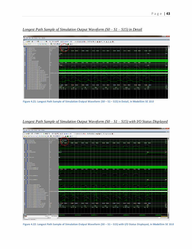
Longest Path Sample of Simulation Output Waveform (S0 – S1 – S15) in Detail
Longest Path Sample of Simulation Output Waveform (S0 – S1 – S15) with I/O Status Displayed
Figure 4.21: Longest Path Sample of Simulation Output Waveform (S0 – S1 – S15) in Detail, in ModelSim SE 10.0
Figure 4.22: Longest Path Sample of Simulation Output Waveform (S0 – S1 – S15) with I/O Status Displayed, in ModelSim SE 10.0
P a g e | 44
CHAPTER 5
Top-Level and Peripheral Component Design
At this point, the design of the System Controller Unit for the Vending Machine Model
was accomplished, and at the same time, the complete simulation and verification was performed
and revealed that the design matches with the initial specification and proposal successfully.
However, this is simply a piece of script that depicts the core of the vending machine model, thus
cannot be implemented directly on an FPGA board, as well as to a real manufactured product.
In order to successfully synthesize and program the final design onto the Spartan-3E
FPGA, the designer must utilize some on-board I/Os such as slide-switch inputs sw(7:0), the
pushbutton inputs btn(3:0), and the LED outputs ld(7:0), and link them with the Vending
Machine Design I/O ports: input_coin_select(4 downto 0) and output_product(2 downto 0) as
portrayed in Section 3.4 above. By observing this situation, the author utilizes the idea of top-
level design method and modularization for this project, in order to integrate these proper
designed I/O ports onto the FPGA board.
Besides, there are some other issues accompanying with the final implementation, which
will be discussed below.
5.1 Top-Level Design and Modularization
The idea of modularization in this project is to divide the whole system into several
independent blocks, and each of them can perform and achieve its design purpose functionally.
Then the designer generates a Top-Level Design file to aggregate all of the components together,
and links the design with specific on-board I/O ports at the same time.
And at this stage, the peripheral components needed are Clock Divider Unit,
Asynchronous Pulse Generator Unit and the Vending Machine System Controller Unit (VM as
abbreviation) that was discussed above. The following is the Top-Level Design Block Diagram:
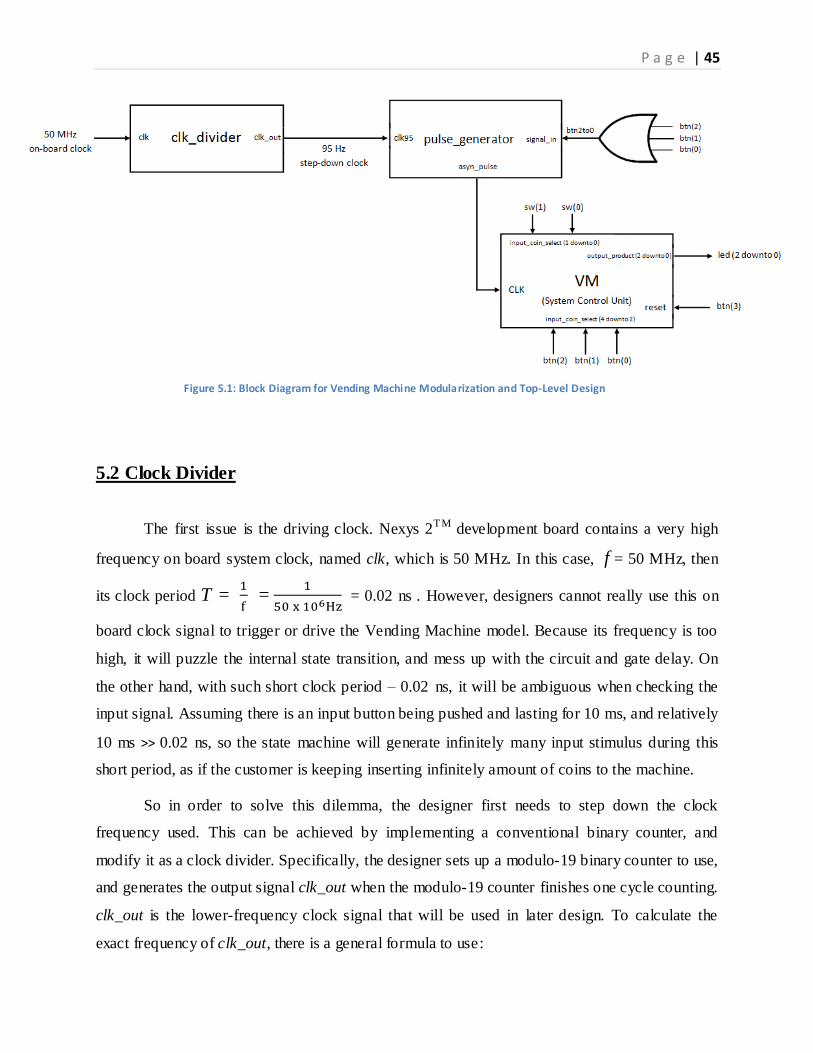
P a g e | 45
5.2 Clock Divider
The first issue is the driving clock. Nexys 2TM development board contains a very high
frequency on board system clock, named clk, which is 50 MHz. In this case, f = 50 MHz, then
its clock period T =
=
= 0.02 ns . However, designers cannot really use this on
board clock signal to trigger or drive the Vending Machine model. Because its frequency is too
high, it will puzzle the internal state transition, and mess up with the circuit and gate delay. On
the other hand, with such short clock period – 0.02 ns, it will be ambiguous when checking the
input signal. Assuming there is an input button being pushed and lasting for 10 ms, and relatively
10 ms >> 0.02 ns, so the state machine will generate infinitely many input stimulus during this
short period, as if the customer is keeping inserting infinitely amount of coins to the machine.
So in order to solve this dilemma, the designer first needs to step down the clock
frequency used. This can be achieved by implementing a conventional binary counter, and
modify it as a clock divider. Specifically, the designer sets up a modulo-19 binary counter to use,
and generates the output signal clk_out when the modulo-19 counter finishes one cycle counting.
clk_out is the lower-frequency clock signal that will be used in later design. To calculate the
exact frequency of clk_out, there is a general formula to use:
Figure 5.1: Block Diagram for Vending Machine Modularization and Top-Level Design
P a g e | 46
fi =
where i is the module of the designed binary counter
So by implementing a modulo-19 binary counter,
f19 =
=
= 95.3674 Hz ≈ 95 Hz
Its clock period,
T =
=
≈ 0.01052 s ≈ 10.5 ms
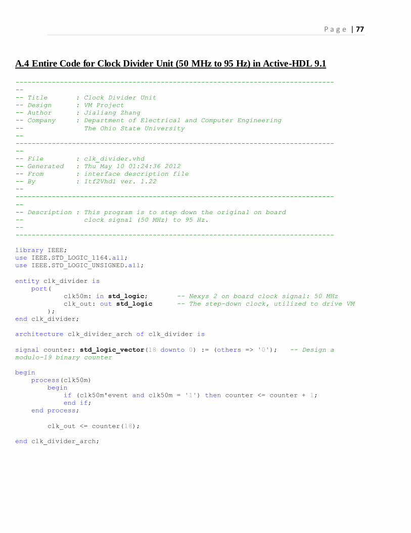
The entire code for this clock divider is listed in Appendix A.4.
And below is the actual simulation waveform of this Clock Divider design, as
demonstrated in Section 4.2 (a snapshot of the simulation waveform in Section 4.2):
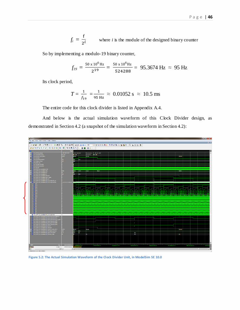
Figure 5.2: The Actual Simulation Waveform of the Clock Divider Unit, in ModelSim SE 10.0
P a g e | 47
In this simulation waveform, counter (0) is equivalent to the on-board clock signal clk,
which frequency is 50 MHz, and counter (18) is equivalent to the desired step-down clock signal
clk95, which frequency is approximate 95 Hz.
5.3 Asynchronous Pulse Generator
The second issue is involved with pushbutton debouncing. Without proper debouncing
function and design, when the customer pushes a button, the input signal will bounce between 0
and 1 for a while. And it will trigger a series of undesired actions inside the sequential circuit.
This is also a typical design problem that any digital designer should be aware of when
implementing pushbutton functions.
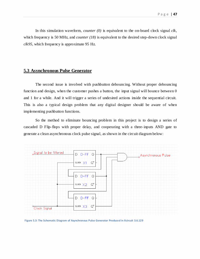
So the method to eliminate bouncing problem in this project is to design a series of
cascaded D Flip- flops with proper delay, and cooperating with a three- inputs AND gate to
generate a clean asynchronous clock pulse signal, as shown in the circuit diagram below:
Figure 5.3: The Schematic Diagram of Asynchronous Pulse Generator Produced in Xcircuit 3.6.129
P a g e | 48
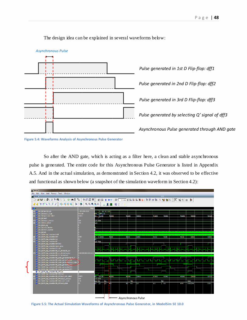
The design idea can be explained in several waveforms below:
So after the AND gate, which is acting as a filter here, a clean and stable asynchronous
pulse is generated. The entire code for this Asynchronous Pulse Generator is listed in Appendix
A.5. And in the actual simulation, as demonstrated in Section 4.2, it was observed to be effective
and functional as shown below (a snapshot of the simulation waveform in Section 4.2):
Asynchronous Pulse
Pulse generated in 1st D Flip-flop: dff1
Pulse generated in 2nd D Flip-flop: dff2
Pulse generated in 3rd D Flip-flop: dff3
Pulse generated by selecting Q’ signal of dff3
Asynchronous Pulse generated through AND gate
Figure 5.4: Waveforms Analysis of Asynchronous Pulse Generator
Figure 5.5: The Actual Simulation Waveforms of Asynchronous Pulse Generator, in ModelSim SE 10.0
Asynchronous Pulse
P a g e | 49
Finally, with the accomplishment of Vending Machine System Controller Unit, Clock
Divider Unit and Asynchronous Pulse Generator Unit, the designer would be able to generate
Top-Level Design file of the model by applying component declaration and instantiation
functions in VHDL, and link internal signals with corresponding on-board I/Os straightforward.
The entire code for this Asynchronous Pulse Generator is listed in Appendix A.6.
P a g e | 50
CHAPTER 6
User Interface Unit Design (Keypad and Display System)
6.1 Product Selection Unit (Keypad System)
Now the keypad system will be designed in VHDL and implemented by FPGA. As stated
in the Vending Machine Design Specifications, there are up to sixteen different kinds of products
available for the designed vending machine. So the little keypad, as designed, should have
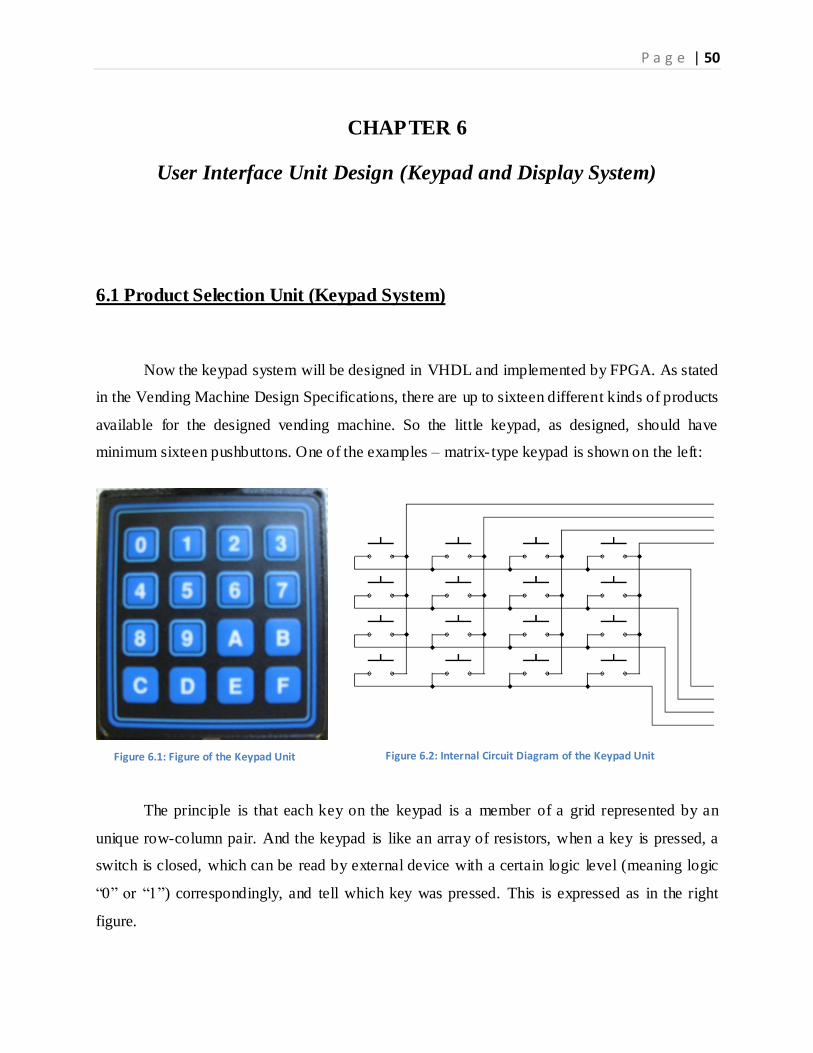
minimum sixteen pushbuttons. One of the examples – matrix- type keypad is shown on the left:
The principle is that each key on the keypad is a member of a grid represented by an
unique row-column pair. And the keypad is like an array of resistors, when a key is pressed, a
switch is closed, which can be read by external device with a certain logic level (meaning logic
“0” or “1”) correspondingly, and tell which key was pressed. This is expressed as in the right
figure.
Figure 6.1: Figure of the Keypad Unit Figure 6.2: Internal Circuit Diagram of the Keypad Unit
P a g e | 51
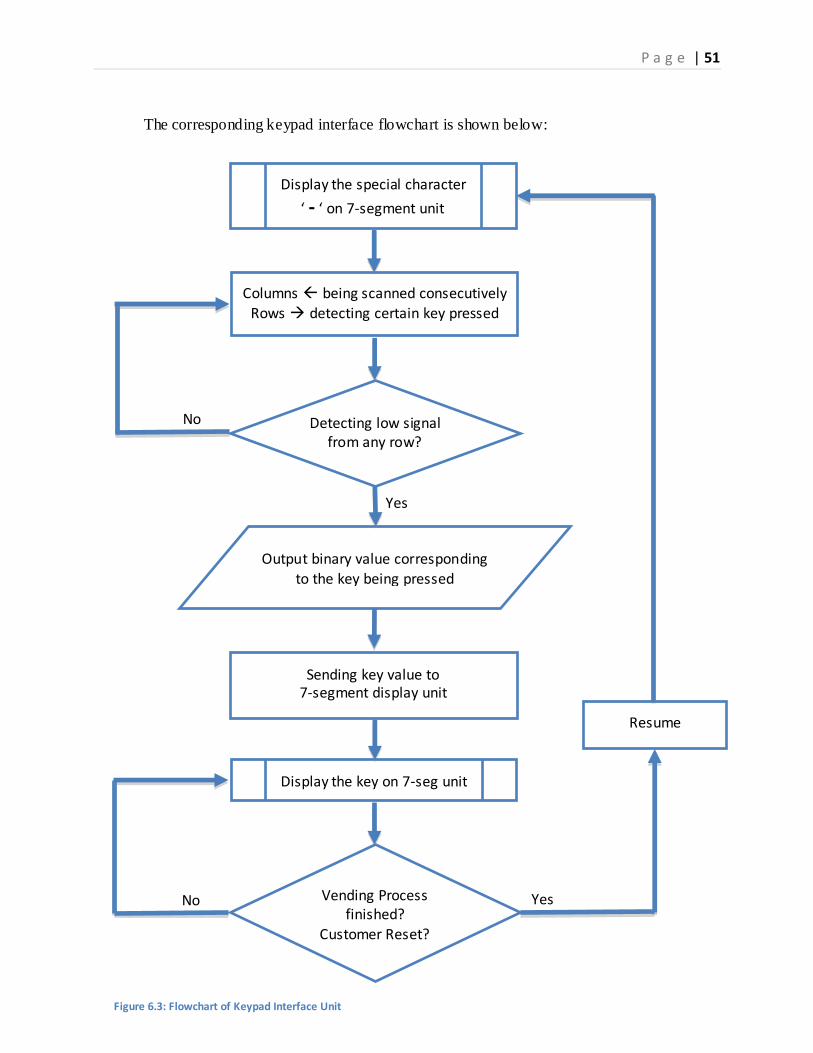
The corresponding keypad interface flowchart is shown below:
Yes
No
Yes
Resume
Vending Process finished?
Customer Reset?
Display the special character
‘ - ‘ on 7-segment unit
Detecting low signal from any row?
Display the key on 7-seg unit
Columns being scanned consecutively
Rows detecting certain key pressed
Output binary value corresponding
to the key being pressed
Sending key value to 7-segment display unit
No
Figure 6.3: Flowchart of Keypad Interface Unit
P a g e | 52
Here is the mechanism of the designed keypad unit: Firstly, the author designed a
modulo-2 binary counter, which is driven by the existing step-down clock signal clk95 from
clock divider discussed in Section 5.2. This modulo-2 binary counter enables the design
idea of consecutive keypad column scanning as following: the modulo -2 binary counter will
count through “00” “01” “10” “11” “00” …. step by step, and at each incremental
step, the designed keypad system unit will ground an unique one of four columns of the
keypad (logic level “0”), while holding the other columns high (logic level “1”). At the same
time, the controller will keep checking each row of the keypad to figure out which key is
being pressed exactly. On the other hand, the use of the much slower clock signal clk95 and
the modulo-2 binary counter will achieve the pushbutton debouncing function, since its
system-cycle is relatively longer than any short-period interfering signal.
Secondly, the design script will immediately assign a corresponding five-digit binary
value to an internal signal signal_out, at each single step if there was a low-level row signal
detected. The internal signal signal_out will serve as identification for the Seven-Segment
Display Unit to present correct vending product selection in hexadecimal number. This is a
one-to-one correspondence. And the transformation is simply a conversion between a five-
digit binary number and a hexadecimal number, except for the very last case when
signal_out is “11111”, which will call to display a special character “ – ”, meaning there is no
valid key being pressed currently. The special character “ – ” will also be the initial display
of the Seven-Segment Display Unit when the design model is powered up.
The whole script for the single keypad unit is attached in the Appendix A.7. The
script of the clock divider is omitted at this time, since it is identical with the one in Section
5.2.
P a g e | 53
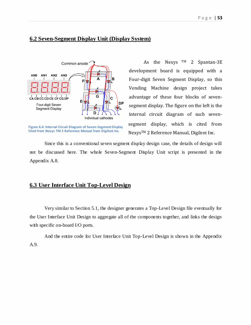
Figure 6.4: Internal Circuit Diagram of Seven-Segment Display Cited from Nexys TM 2 Reference Manual from Digilent Inc.
6.2 Seven-Segment Display Unit (Display System)
As the Nexys TM 2 Spantan-3E
development board is equipped with a
Four-digit Seven Segment Display, so this
Vending Machine design project takes
advantage of these four blocks of seven-
segment display. The figure on the left is the
internal circuit diagram of such seven-
segment display, which is cited from
NexysTM 2 Reference Manual, Digilent Inc.
Since this is a conventional seven segment display design case, the details of design will
not be discussed here. The whole Seven-Segment Display Unit script is presented in the
Appendix A.8.
6.3 User Interface Unit Top-Level Design
Very similar to Section 5.1, the designer generates a Top-Level Design file eventually for
the User Interface Unit Design to aggregate all of the components together, and links the design
with specific on-board I/O ports.
And the entire code for User Interface Unit Top-Level Design is shown in the Appendix
A.9.
P a g e | 54
CHAPTER 7
Final Vending Machine Design
In this final design, the author is going to integrate all the components, such as System
Controller Unit (Control Center), Clock Divider Unit, Asynchronous Pulse Generator Unit,
Product Selection Unit and Seven-Segment Display Unit. However, it is not simply to add up all
the above components into a single Top-Level design file, there are several internal- flow signals
added or modified. Besides, the Seven-Segment Display Unit needs to be redesigned and
improved greatly, with some new adding functions. And in this final design file, it will be
renamed as Improved Four-Digit Seven-Segment Display Unit as discussed below.
7.1 Clock Divider Unit (50 MHz to 1.5 KHz & 95 Hz)
It is an inevitable physical constraint that the FPGA can only enable and display one
single digit of the four-digit seven-segment display at one time. However, if the designer raises
the flashing rate and keeps flashing all of the four digits sequentially, at the customer end, it will
seem like all the data is presenting together simultaneously. By this approach, it will also achieve
the goal to update the dynamic vending information immediately. So the very first procedure is
to generate a new clock signal with “high-enough” frequency, which is clk1500 in the script.
With identical design idea of clk95 as demonstrated in Section 5.2, clk1500 signal takes the
output signal of counter (14) from a modulo-19 binary counter:
f15 =
=
= 1525.8789 Hz ≈ 1.5 KHz
Its clock period,
T =
=
≈ 0.66667 s
The entire code for this newly designed clock divider is listed in Appendix A.10.
P a g e | 55
Asynchronous Pulse Generator Unit will remain the same as the initial design, so it will
not be discussed in this section again.
7.2 Flag Signal Modification
The second component to be integrated is the Product Selection Unit (Keypad System).
Besides the existing I/Os and internal signals in the original design, the author added in another
internal flag signal prod_signal (1 downto 0). The signal prod_signal contains three possible
values, namely “01”, “10” and “00”. Obviously, “01”, “10” indicates the vending machine
customer selects a product of $1.00, $1.25 correspondingly. And for the case “00”, it has two
possibilities: one as the initial state, the other is the indication that the customer selects a product
of $1.50, which is the identical design idea as discussed in Section 3.4. For the vending purpose,
the customer has to make a selection beforehand, thus when the machine is processing the
vending, prod_signal with value “00” always means that the user selects a product of $1.50,
which is simple and unambiguous. Signal prod_signal is used to communicate with the input
signal input_coin_select (1 downto 0) of System Controller Unit Design, as a replacement of
slide switches input sw (1 downto 0).
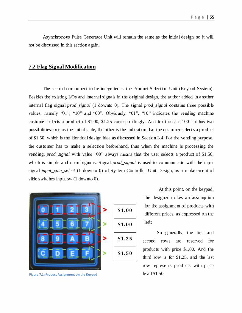
At this point, on the keypad,
the designer makes an assumption
for the assignment of products with
different prices, as expressed on the
left:
So generally, the first and
second rows are reserved for
products with price $1.00. And the
third row is for $1.25, and the last
row represents products with price
level $1.50. Figure 7.1: Product Assignment on the Keypad
P a g e | 56
The entire code for this modified Product Selection Unit (Keypad System) is listed in
Appendix A.11.
Similar to Product Selection Unit, the third component System Controller Unit (Control
Center) is also modified with an internal signal price_id added. Signal price_id is a fifteen-digit
size bit_vector, which can be divided into three groups of five-digit size sub-vectors. Based on
binary value to decimal number conversion, each sub-vector represents a decimal number, like
“0”, “1”, “2” and “5” typically. Signal price_id is targeted as identification, inserted into every
single state in the State_transition process of System Controller Unit. With the flashing
mechanism, it will display the updated data about vending money/coins on first three digits of
the Improved Four-Digit Seven-Segment Display Unit.
The entire code for this modified System Controller Unit (Control Center) is listed in
Appendix A.12.
7.3 Improved Four-Digit Seven-Segment Display Unit (Display System)
As expressed in the title of the script “Improved Four-Digit Seven-Segment Display Unit
for Price Indication and Product Display (fourdigit_7seg)”, this improved display unit serves two
roles -- dedicated to display the unique product that the customer selects during vending process,
range from Hexadecimal value Pro#1, Pro#2, ... Pro#E to Pro#F, and locates only on the right-
most digit of the four on-board Seven-Segment Display; and to display the actual amount of
money/coins inserted dynamically, which locates on the first three digits of the four on-board
Seven-Segment Display. For example: 1.55 indicates the vending machine accepts one dollar and
fifty- five cents already.
At the same, it will take advantage of the two added flag signal prod_id and price_id.
The entire code for this Improved Four-Digit Seven-Segment Display Unit (Display
System) is listed in Appendix A.13.
P a g e | 57
7.4 Final Vending Machine Top-Level Design
Finally, the Top-Level Design of the Vending Machine integrates all the components
discussed above, and link them accordingly to on-board I/Os. The Vending Machine Project
VHDL Design is eventually completed by doing so.
The entire code for the Final Vending Machine Top-Level Design is listed in Appendix
A.14.
P a g e | 58
CHAPTER 8
Synthesis
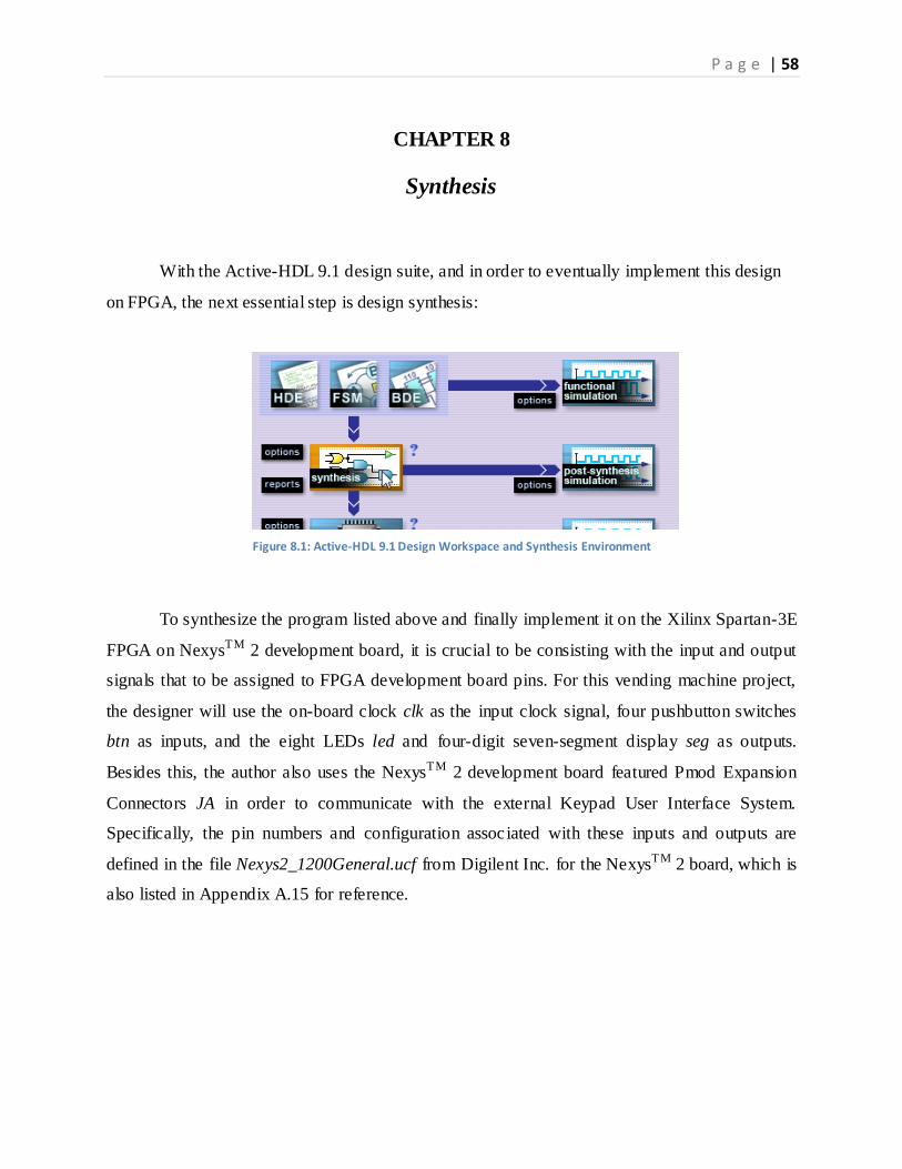
With the Active-HDL 9.1 design suite, and in order to eventually implement this design
on FPGA, the next essential step is design synthesis:
To synthesize the program listed above and finally implement it on the Xilinx Spartan-3E
FPGA on NexysTM 2 development board, it is crucial to be consisting with the input and output
signals that to be assigned to FPGA development board pins. For this vending machine project,
the designer will use the on-board clock clk as the input clock signal, four pushbutton switches
btn as inputs, and the eight LEDs led and four-digit seven-segment display seg as outputs.
Besides this, the author also uses the NexysTM 2 development board featured Pmod Expansion
Connectors JA in order to communicate with the external Keypad User Interface System.
Specifically, the pin numbers and configuration associated with these inputs and outputs are
defined in the file Nexys2_1200General.ucf from Digilent Inc. for the NexysTM 2 board, which is
also listed in Appendix A.15 for reference.
Figure 8.1: Active-HDL 9.1 Design Workspace and Synthesis Environment
P a g e | 59
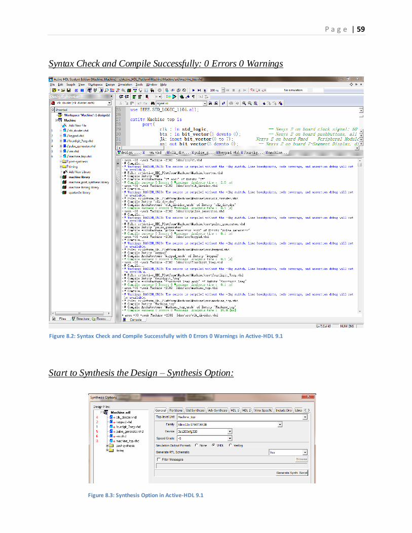
Syntax Check and Compile Successfully: 0 Errors 0 Warnings
Start to Synthesis the Design – Synthesis Option:
Figure 8.2: Syntax Check and Compile Successfully with 0 Errors 0 Warnings in Active-HDL 9.1
Figure 8.3: Synthesis Option in Active-HDL 9.1
P a g e | 60
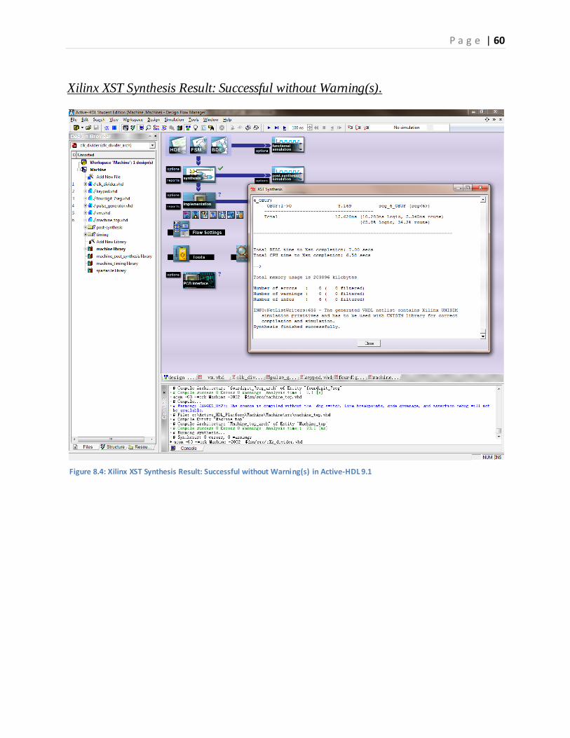
Xilinx XST Synthesis Result: Successful without Warning(s).
Figure 8.4: Xilinx XST Synthesis Result: Successful without Warning(s) in Active-HDL 9.1
P a g e | 61
CHAPTER 9
Implementation
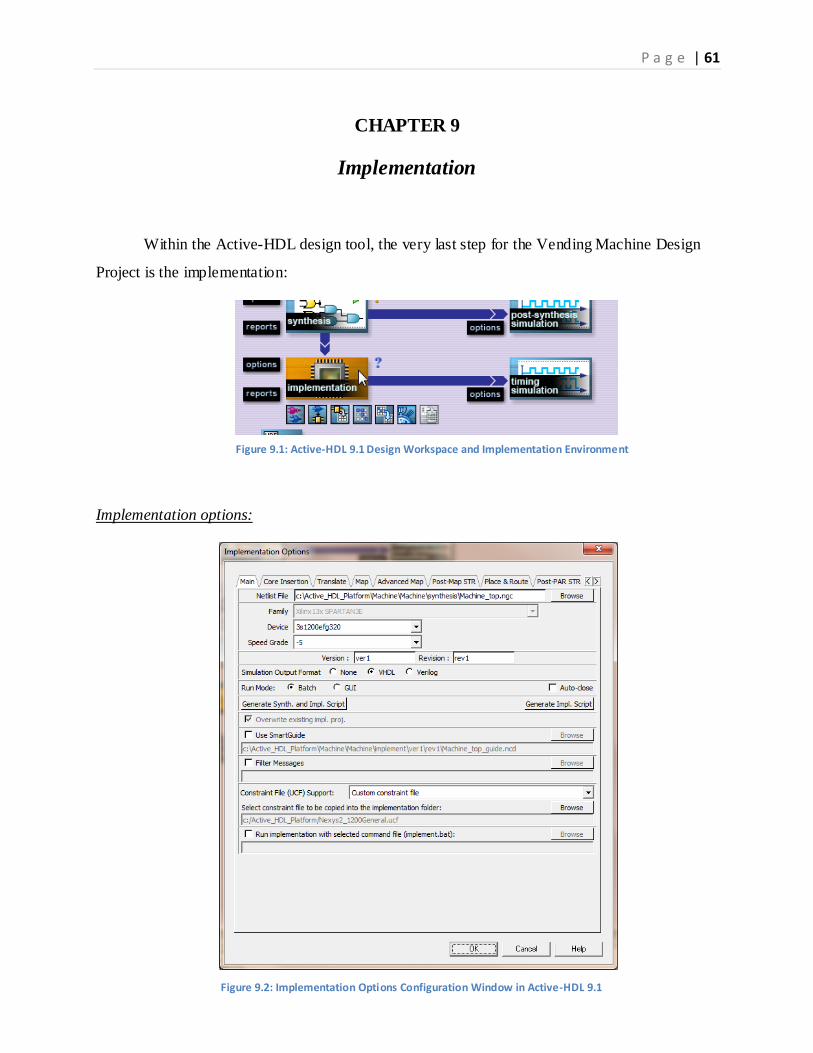
Within the Active-HDL design tool, the very last step for the Vending Machine Design
Project is the implementation:
Implementation options:
Figure 9.1: Active-HDL 9.1 Design Workspace and Implementation Environment
Figure 9.2: Implementation Options Configuration Window in Active-HDL 9.1
P a g e | 62
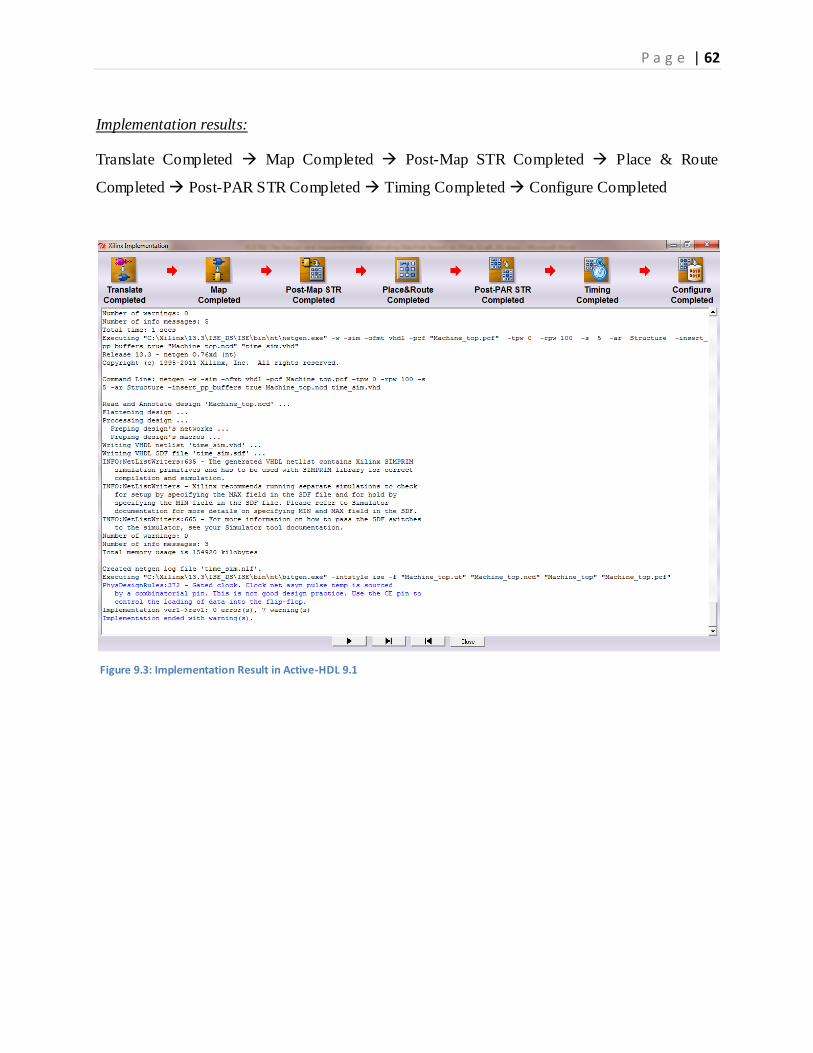
Implementation results:
Translate Completed Map Completed Post-Map STR Completed Place & Route
Completed Post-PAR STR Completed Timing Completed Configure Completed
Figure 9.3: Implementation Result in Active-HDL 9.1
P a g e | 63
CHAPTER 10
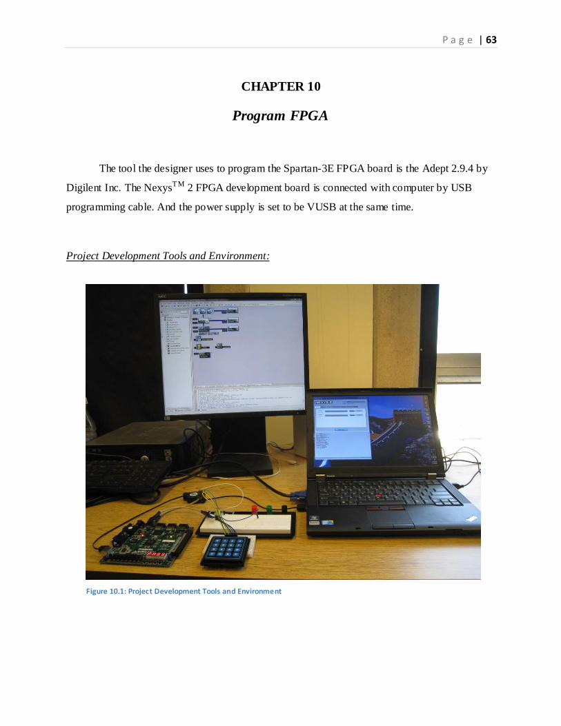
Program FPGA
The tool the designer uses to program the Spartan-3E FPGA board is the Adept 2.9.4 by
Digilent Inc. The NexysTM 2 FPGA development board is connected with computer by USB
programming cable. And the power supply is set to be VUSB at the same time.
Project Development Tools and Environment:
Figure 10.1: Project Development Tools and Environment
P a g e | 64
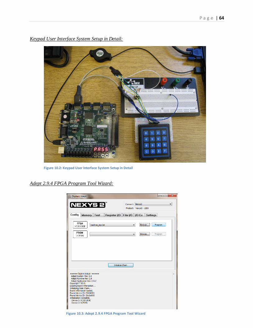
Keypad User Interface System Setup in Detail:
Adept 2.9.4 FPGA Program Tool Wizard:
Figure 10.2: Keypad User Interface System Setup in Detail
Figure 10.3: Adept 2.9.4 FPGA Program Tool Wizard
P a g e | 65
CHAPTER 11
Conclusion
The Design, Simulation, Verification and Implementation of Vending Machine Based on
FPGA has been demonstrated and completed successfully. From Design Proposal, various
components designed in VHDL, to simulation, verification and final implementation, the entire
design project can be considered as a whole process of typical digital circuit design in real life.
With a detailed review over each step of the design project, it should be noticed that a
Complete Simulation and Verification plays an important role in the accomplishment of the
project. All the major program debugging and design revisions are emerged and realized through
this project procedure. And it consumed most of the time and effort spending on the project,
though.
On the other hand, program modulation and top-level design significantly improves the
efficiency, interchangeability and feasibility of the vending machine design project. It makes the
designer more easily to debug, maintain, transfer and integrate each functional block, and
eventually to achieve the timely completion of a complex digital circuit design project.
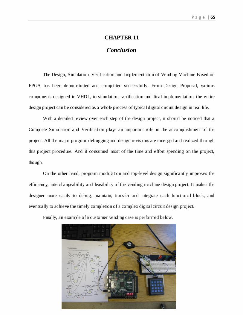
Finally, an example of a customer vending case is performed below.
P a g e | 66
References:
Digilent Nexys 2 Board Reference Manual. July 11, 2011. <http://www.digilentinc.com>
Haskell, R. E. and Hanna, D. M. Digital Design Using Digilent FPGA Boards – VHDL/Active-
HDL Edition. Rochester Hills, MI: LBE Books, 2009. Print.
Wakerly, J. F. Digital Design: Principles and Practices, 4th Ed. Upper Saddle River, NJ: Pearson
/ Prentice Hall, 2006. Print.
Xilinx Web. N.p. April 2011. Web. 9 April 2011. <http://www.xilinx.com/>
Yokouchi, T. (2010). Today and Tomorrow of Vending Machine and its Services in Japan.
Service Systems and Servece Management (ICSSSM), 2010 7th International Conference.
28-30 Jun, 2010. Retrieved from IEEE Xplore Digital Library.
Zainuddin, F.; Ali, N. M. & Sidek, R. M. et al. Conceptual modeling for simulation: Steaming
frozen food processing in vending machine. Computer Science ad Information
Technology, 2009. 2nd IEEE International Conference. 8-11 Aug, 2010. Retrieved from
IEEE Xplore Digital Library.
P a g e | 67
Appendix
A.1 Entire Code for System Controller Unit Design (FPGA) in Active-HDL 9.1
-------------------------------------------------------------------------------
-- Title : Vending Machine System Controller Unit
-- Design : VM Project
-- Author : Jialiang Zhang
-- Company : Department of Electrical and Computer Engineering
-- The Ohio State University
--
-------------------------------------------------------------------------------
--
-- File : VM.vhd
-- Generated : Fri Mar 2 10:58:42 2012
-- From : interface description file
-- By : Itf2Vhdl ver. 1.22
--
-------------------------------------------------------------------------------
--
-- Description : Major debugging and revision, this is the final script
-- transferred from Xilinx ISE Design Suite 13.3
--
-----------------------------------------------------------------------------
library IEEE;
use IEEE.STD_LOGIC_1164.all;
entity VM is
port(
CLK : in bit;
reset : in bit;
input_coin_select : in bit_vector(4 downto 0);
output_product : out bit_vector(2 downto 0)
);
end VM;
architecture VM_arch of VM is
type statetype is (S0,S1,S2,S3,S4A,S4B,S5A,S5B,S6,S7,S8,S9,S10,S11,S12A,S12B,S13,S14,S15);
signal current_state,next_state: statetype;
begin
Sequential: process(reset,CLK)
begin
if reset = '1' then current_state <= S0;
elsif (CLK'event and CLK='1') then current_state <= next_state;
end if;
end process;
State_transition: process(current_state,input_coin_select)
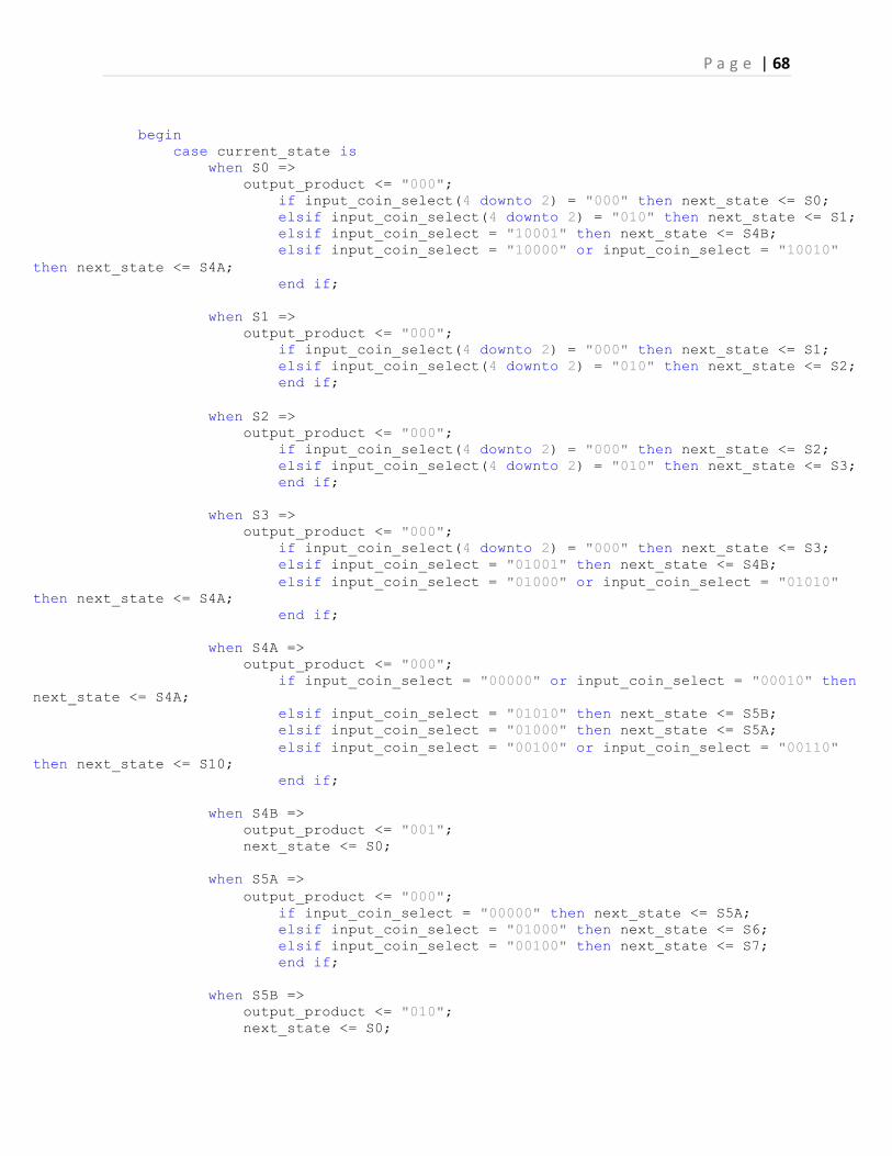
P a g e | 68
begin
case current_state is
when S0 =>
output_product <= "000";
if input_coin_select(4 downto 2) = "000" then next_state <= S0;
elsif input_coin_select(4 downto 2) = "010" then next_state <= S1;
elsif input_coin_select = "10001" then next_state <= S4B;
elsif input_coin_select = "10000" or input_coin_select = "10010"
then next_state <= S4A;
end if;
when S1 =>
output_product <= "000";
if input_coin_select(4 downto 2) = "000" then next_state <= S1;
elsif input_coin_select(4 downto 2) = "010" then next_state <= S2;
end if;
when S2 =>
output_product <= "000";
if input_coin_select(4 downto 2) = "000" then next_state <= S2;
elsif input_coin_select(4 downto 2) = "010" then next_state <= S3;
end if;
when S3 =>
output_product <= "000";
if input_coin_select(4 downto 2) = "000" then next_state <= S3;
elsif input_coin_select = "01001" then next_state <= S4B;
elsif input_coin_select = "01000" or input_coin_select = "01010"
then next_state <= S4A;
end if;
when S4A =>
output_product <= "000";
if input_coin_select = "00000" or input_coin_select = "00010" then
next_state <= S4A;
elsif input_coin_select = "01010" then next_state <= S5B;
elsif input_coin_select = "01000" then next_state <= S5A;
elsif input_coin_select = "00100" or input_coin_select = "00110"
then next_state <= S10;
end if;
when S4B =>
output_product <= "001";
next_state <= S0;
when S5A =>
output_product <= "000";
if input_coin_select = "00000" then next_state <= S5A;
elsif input_coin_select = "01000" then next_state <= S6;
elsif input_coin_select = "00100" then next_state <= S7;
end if;
when S5B =>
output_product <= "010";
next_state <= S0;
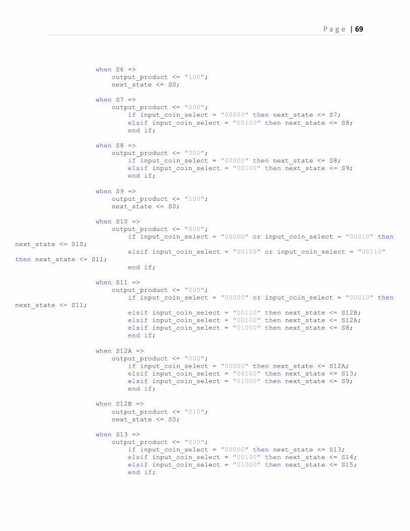
P a g e | 69
when S6 =>
output_product <= "100";
next_state <= S0;
when S7 =>
output_product <= "000";
if input_coin_select = "00000" then next_state <= S7;
elsif input_coin_select = "00100" then next_state <= S8;
end if;
when S8 =>
output_product <= "000";
if input_coin_select = "00000" then next_state <= S8;
elsif input_coin_select = "00100" then next_state <= S9;
end if;
when S9 =>
output_product <= "100";
next_state <= S0;
when S10 =>
output_product <= "000";
if input_coin_select = "00000" or input_coin_select = "00010" then
next_state <= S10;
elsif input_coin_select = "00100" or input_coin_select = "00110"
then next_state <= S11;
end if;
when S11 =>
output_product <= "000";
if input_coin_select = "00000" or input_coin_select = "00010" then
next_state <= S11;
elsif input_coin_select = "00110" then next_state <= S12B;
elsif input_coin_select = "00100" then next_state <= S12A;
elsif input_coin_select = "01000" then next_state <= S8;
end if;
when S12A =>
output_product <= "000";
if input_coin_select = "00000" then next_state <= S12A;
elsif input_coin_select = "00100" then next_state <= S13;
elsif input_coin_select = "01000" then next_state <= S9;
end if;
when S12B =>
output_product <= "010";
next_state <= S0;
when S13 =>
output_product <= "000";
if input_coin_select = "00000" then next_state <= S13;
elsif input_coin_select = "00100" then next_state <= S14;
elsif input_coin_select = "01000" then next_state <= S15;
end if;
P a g e | 70
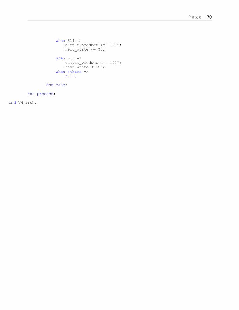
when S14 =>
output_product <= "100";
next_state <= S0;
when S15 =>
output_product <= "100";
next_state <= S0;
when others =>
null;
end case;
end process;
end VM_arch;
P a g e | 71
A.2 Entire Code for Simulation and Verification Testbench in Section 4.2 in ModelSim SE 10.0
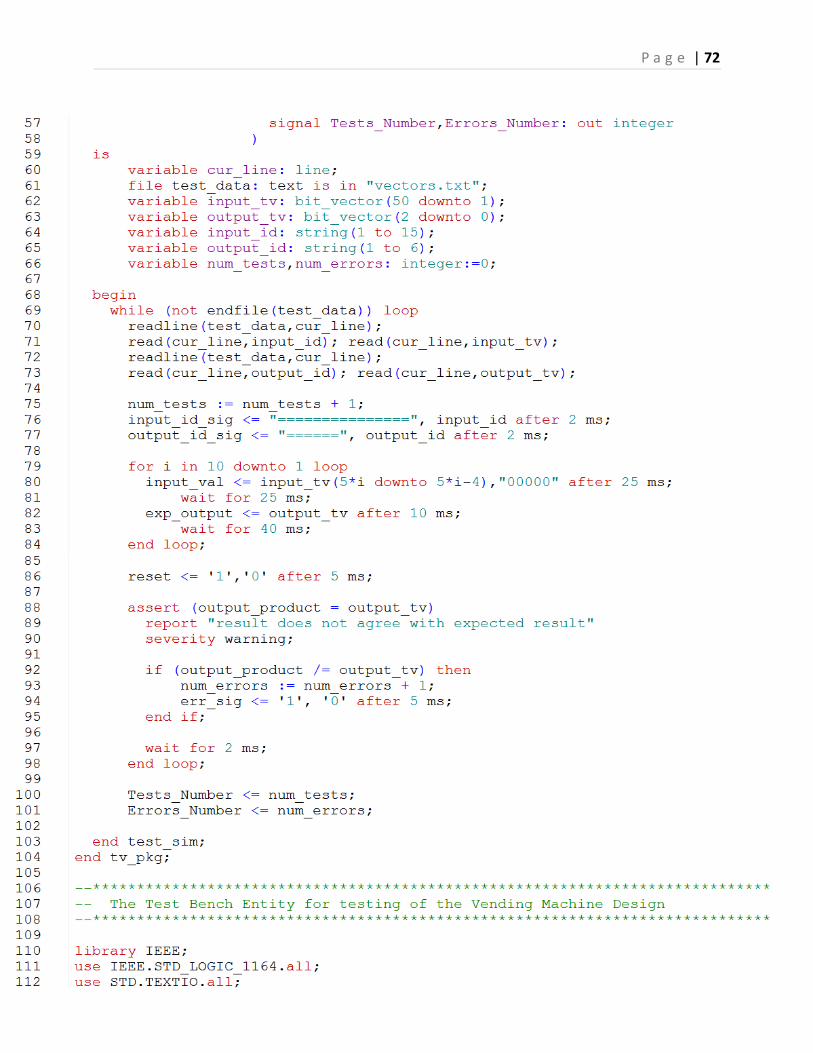
P a g e | 72
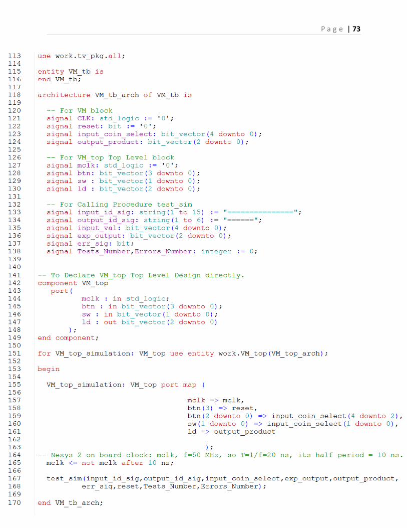
P a g e | 73
P a g e | 74
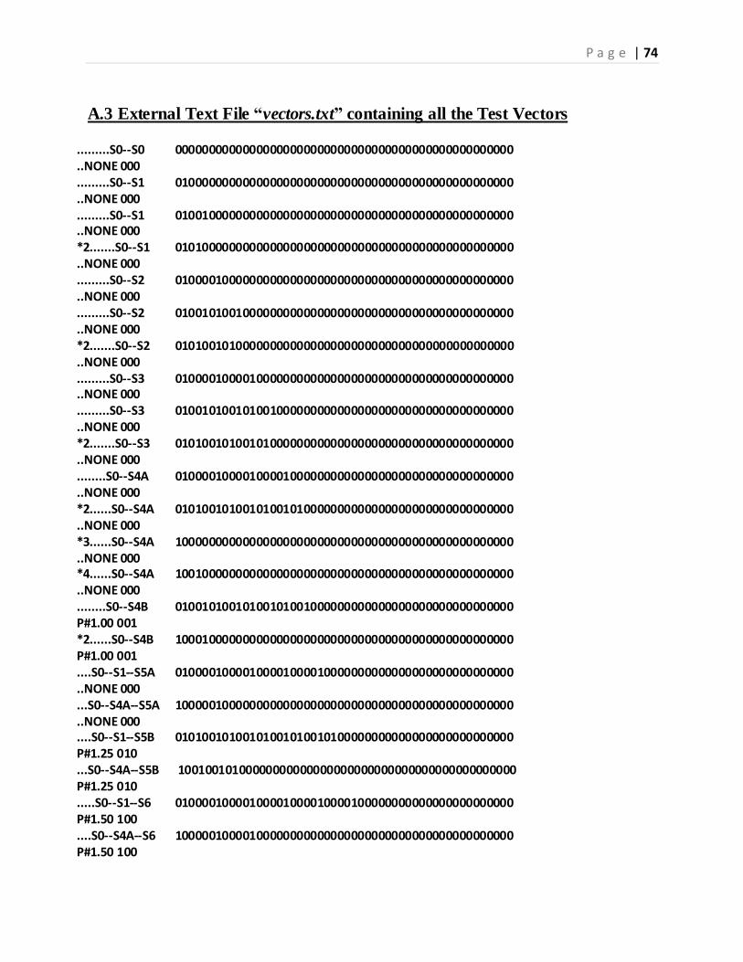
A.3 External Text File “vectors.txt” containing all the Test Vectors
.........S0--S0 00000000000000000000000000000000000000000000000000
..NONE 000
.........S0--S1 01000000000000000000000000000000000000000000000000
..NONE 000
.........S0--S1 01001000000000000000000000000000000000000000000000
..NONE 000 *2.......S0--S1 01010000000000000000000000000000000000000000000000 ..NONE 000 .........S0--S2 01000010000000000000000000000000000000000000000000 ..NONE 000 .........S0--S2 01001010010000000000000000000000000000000000000000 ..NONE 000 *2.......S0--S2 01010010100000000000000000000000000000000000000000 ..NONE 000 .........S0--S3 01000010000100000000000000000000000000000000000000 ..NONE 000 .........S0--S3 01001010010100100000000000000000000000000000000000 ..NONE 000 *2.......S0--S3 01010010100101000000000000000000000000000000000000 ..NONE 000 ........S0--S4A 01000010000100001000000000000000000000000000000000 ..NONE 000 *2......S0--S4A 01010010100101001010000000000000000000000000000000 ..NONE 000 *3......S0--S4A 10000000000000000000000000000000000000000000000000 ..NONE 000 *4......S0--S4A 10010000000000000000000000000000000000000000000000 ..NONE 000 ........S0--S4B 01001010010100101001000000000000000000000000000000 P#1.00 001 *2......S0--S4B 10001000000000000000000000000000000000000000000000 P#1.00 001 ....S0--S1--S5A 01000010000100001000010000000000000000000000000000 ..NONE 000 ...S0--S4A--S5A 10000010000000000000000000000000000000000000000000 ..NONE 000 ....S0--S1--S5B 01010010100101001010010100000000000000000000000000 P#1.25 010 ...S0--S4A--S5B 10010010100000000000000000000000000000000000000000 P#1.25 010 .....S0--S1--S6 01000010000100001000010000100000000000000000000000 P#1.50 100 ....S0--S4A--S6 10000010000100000000000000000000000000000000000000 P#1.50 100
P a g e | 75
.....S0--S1--S7 01000010000100001000010000010000000000000000000000
..NONE 000
....S0--S4A--S7 10000010000010000000000000000000000000000000000000
..NONE 000
.....S0--S1--S8 01000010000100001000010000010000100000000000000000
..NONE 000
....S0--S4A--S8 10000010000010000100000000000000000000000000000000
..NONE 000
...S0--S1-S7-S9 01000010000100001000010000010000100001000000000000 P#1.50 100 ...S0-S4A-S7-S9 10000010000010000100001000000000000000000000000000 P#1.50 100 ...S0-S1-S10-S9 01000010000100001000001000010000100010000000000000 P#1.50 100 ..S0-S4A-S10-S9 10000001000010000100010000000000000000000000000000 P#1.50 100 ....S0--S1--S10 01000010000100001000001000000000000000000000000000 ..NONE 000 *2..S0--S1--S10 01010010100101001010001100000000000000000000000000 ..NONE 000 ...S0--S4A--S10 10000001000000000000000000000000000000000000000000 ..NONE 000 *2.S0--S4A--S10 10010001100000000000000000000000000000000000000000 ..NONE 000 ....S0--S1--S11 01000010000100001000001000010000000000000000000000 ..NONE 000 *2..S0--S1--S11 01010010100101001010001100011000000000000000000000 ..NONE 000 ...S0--S4A--S11 10000001000010000000000000000000000000000000000000 ..NONE 000 *2.S0--S4A--S11 10010001100011000000000000000000000000000000000000 ..NONE 000 ...S0--S1--S12A 01000010000100001000001000010000100000000000000000 ..NONE 000 ..S0--S4A--S12A 10000001000010000100000000000000000000000000000000 ..NONE 000 ...S0--S1--S12B 01010010100101001010001100011000110000000000000000 P#1.25 010 ..S0--S4A--S12B 10010001100011000110000000000000000000000000000000 P#1.25 010 ....S0--S1--S13 01000010000100001000001000010000100001000000000000 ..NONE 000 ...S0--S4A--S13 10000001000010000100001000000000000000000000000000 ..NONE 000 ....S0--S1--S14 01000010000100001000001000010000100001000010000000 P#1.50 100 ...S0--S4A--S14 10000001000010000100001000010000000000000000000000
P a g e | 76
P#1.50 100 ....S0--S1--S15 01000010000100001000001000010000100001000100000000 P#1.50 100 ...S0--S4A--S15 10000001000010000100001000100000000000000000000000 P#1.50 100
P a g e | 77
A.4 Entire Code for Clock Divider Unit (50 MHz to 95 Hz) in Active-HDL 9.1
-------------------------------------------------------------------------------
--
-- Title : Clock Divider Unit
-- Design : VM Project
-- Author : Jialiang Zhang
-- Company : Department of Electrical and Computer Engineering
-- The Ohio State University
--
-------------------------------------------------------------------------------
--
-- File : clk_divider.vhd
-- Generated : Thu May 10 01:24:36 2012
-- From : interface description file
-- By : Itf2Vhdl ver. 1.22
--
-------------------------------------------------------------------------------
--
-- Description : This program is to step down the original on board
-- clock signal (50 MHz) to 95 Hz.
--
-------------------------------------------------------------------------------
library IEEE;
use IEEE.STD_LOGIC_1164.all;
use IEEE.STD_LOGIC_UNSIGNED.all;
entity clk_divider is
port(
clk50m: in std_logic; -- Nexys 2 on board clock signal: 50 MHz
clk_out: out std_logic -- The step-down clock, utilized to drive VM
);
end clk_divider;
architecture clk_divider_arch of clk_divider is
signal counter: std_logic_vector(18 downto 0) := (others => '0'); -- Design a
modulo-19 binary counter
begin
process(clk50m)
begin
if (clk50m'event and clk50m = '1') then counter <= counter + 1;
end if;
end process;
clk_out <= counter(18);
end clk_divider_arch;
P a g e | 78
A.5 Entire Code for Asynchronous Pulse Generator Unit in Active-HDL 9.1
-------------------------------------------------------------------------------
--
-- Title : Asynchronous Pulse Generator Unit
-- Design : VM Project
-- Author : Jialiang Zhang
-- Company : Department of Electrical and Computer Engineering
-- The Ohio State University
--
-------------------------------------------------------------------------------
--
-- File : pulse_generator.vhd
-- Generated : Thu May 10 14:56:23 2012
-- From : interface description file
-- By : Itf2Vhdl ver. 1.22
--
-------------------------------------------------------------------------------
--
-- Description : This program is to generate a single clean asynchronous clock
-- pulse that will trigger the Vending Machine Model, and to act
-- as a push-button debouncing unit as well.
--
-------------------------------------------------------------------------------
library IEEE;
use IEEE.STD_LOGIC_1164.all;
entity pulse_generator is
port(
signal_in: in bit; -- input signal to be filtered
clk95: in std_logic;
asyn_pulse: out bit -- generated asynchronous pulse
);
end pulse_generator;
architecture pulse_generator_arch of pulse_generator is
signal dff1,dff2,dff3: bit; -- dff1 & dff2: Q output signal of 1st & 2nd D Flip-flops
-- dff3: Q' output signal of the 3rd D Flip-flops
begin
process(clk95)
begin
if (clk95'event and clk95 = '1') then
dff1 <= signal_in;
dff2 <= dff1;
dff3 <= dff2;
end if;
end process;
asyn_pulse <= dff1 and dff2 and (not dff3); -- three inputs AND gate
end pulse_generator_arch;
P a g e | 79
A.6 Entire Code for Vending Machine Top-Level Design Unit in Active-HDL 9.1
-------------------------------------------------------------------------------
--
-- Title : Vending Machine Top Level Design Unit
-- Design : VM Project
-- Author : Jialiang Zhang
-- Company : Department of Electrical and Computer Engineering
-- The Ohio State University
--
-------------------------------------------------------------------------------
--
-- File : VM_top.vhd
-- Generated : Wed Mar 7 17:52:53 2012
-- From : interface description file
-- By : Itf2Vhdl ver. 1.22
--
-------------------------------------------------------------------------------
--
-- Description : VM_top, top-level design file, the file to be synthesized and
-- implemented on FPGA and Nexys 2 development board.
--
-------------------------------------------------------------------------------
library IEEE;
use IEEE.STD_LOGIC_1164.all;
entity VM_top is
port(
clk : in std_logic; -- Nexys 2 on board clock signal: 50 MHz
btn : in bit_vector(3 downto 0); -- Nexys 2 on board pushbuttons, all of 4 in use
sw : in bit_vector(1 downto 0); -- Nexys 2 on board slide switches, right-most 2 in use
led : out bit_vector(2 downto 0) -- Nexys 2 on board LEDs, right-most 3 in use
);
end VM_top;
architecture VM_top_arch of VM_top is
-- Component declaration of the "clk_divider(clk_divider_arch)" unit defined in
-- file: "./src/clk_divider.vhd"
component clk_divider
port(
clk50m: in std_logic; -- Nexys 2 on board clock signal: 50 MHz
clk_out: out std_logic -- The step-down clock, utilized to drive VM
);
end component;
for lbl_clk_divider: clk_divider use entity work.clk_divider(clk_divider_arch);
-- Component declaration of the "pulse_generator(pulse_generator_arch)" unit defined in
-- file: "./src/pulse_generator.vhd"
component pulse_generator
port(
signal_in: in bit; -- input signal to be filtered
clk95: in std_logic; -- use the step-down 95 Hz clock signal
asyn_pulse: out bit -- generated asynchronous pulse
P a g e | 80
);
end component;
for lbl_pulse_generator: pulse_generator use entity
work.pulse_generator(pulse_generator_arch);
-- Component declaration of the "VM(VM_arch)" unit defined in
-- file: "./src/VM.vhd"
component VM
port(
CLK : in bit;
reset : in bit;
input_coin_select : in bit_vector(4 downto 0);
output_product : out bit_vector(2 downto 0)
);
end component;
for lbl_VM: VM use entity work.VM(VM_arch);
signal btn2to0,asyn_pulse_temp: bit;
signal clk_out_temp: std_logic;
begin
btn2to0 <= btn(2) or btn(1) or btn(0);
lbl_clk_divider : clk_divider port map( clk50m => clk,
clk_out => clk_out_temp);
lbl_pulse_generator : pulse_generator port map( signal_in => btn2to0,
clk95 => clk_out_temp,
asyn_pulse => asyn_pulse_temp);
lbl_VM : VM port map(
CLK => asyn_pulse_temp, -- generated asynchronous clock
signal
reset => btn(3), -- left-most pushbutton on Nexys
2 board, Reset Function,
input_coin_select(4 downto 2) => btn(2 downto 0), --
rest three pushbuttons, coin inserting stimulus
input_coin_select(1 downto 0) => sw(1 downto 0), --
right-most two slide switches, customer's selection indication
output_product => led
);
end VM_top_arch;
P a g e | 81
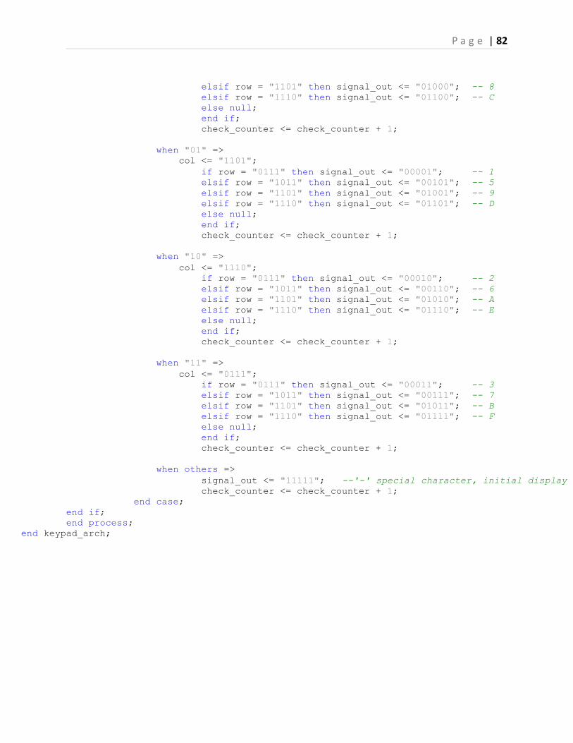
A.7 Entire Code for Product Selection Unit (Keypad System) in Active-HDL 9.1
-------------------------------------------------------------------------------
--
-- Title : Product Selection Unit
-- Design : VM_keypad Project
-- Author : Jialiang Zhang
-- Company : Department of Electrical and Computer Engineering
-- The Ohio State University
--
-------------------------------------------------------------------------------
--
-- File : keypad.vhd
-- Generated : Tue April 22 13:31:44 2012
-- From : interface description file
-- By : Itf2Vhdl ver. 1.22
--
-------------------------------------------------------------------------------
--
-- Description : This is the Keypad Central Controller Unit program
--
-------------------------------------------------------------------------------
library IEEE;
use IEEE.STD_LOGIC_1164.all;
use IEEE.STD_LOGIC_UNSIGNED.all;
entity keypad is
port (
clk95: in std_logic;
reset: in std_logic := '0';
col: out std_logic_vector(3 downto 0);
row: in std_logic_vector(3 downto 0);
signal_out: out std_logic_vector(4 downto 0) := "11111"
);
end keypad;
architecture keypad_arch of keypad is
signal check_counter: std_logic_vector(1 downto 0) := "00"; -- Design a modulo-2 binary counter
begin
process(clk95,reset)
begin
if reset = '1' then check_counter <= "00";
signal_out <= "11111";
elsif (clk95'event and clk95='1') then
case check_counter is
when "00" =>
col <= "1011";
if row = "0111" then signal_out <= "00000"; -- 0
elsif row = "1011" then signal_out <= "00100"; -- 4
P a g e | 82
elsif row = "1101" then signal_out <= "01000"; -- 8
elsif row = "1110" then signal_out <= "01100"; -- C
else null;
end if;
check_counter <= check_counter + 1;
when "01" =>
col <= "1101";
if row = "0111" then signal_out <= "00001"; -- 1
elsif row = "1011" then signal_out <= "00101"; -- 5
elsif row = "1101" then signal_out <= "01001"; -- 9
elsif row = "1110" then signal_out <= "01101"; -- D
else null;
end if;
check_counter <= check_counter + 1;
when "10" =>
col <= "1110";
if row = "0111" then signal_out <= "00010"; -- 2
elsif row = "1011" then signal_out <= "00110"; -- 6
elsif row = "1101" then signal_out <= "01010"; -- A
elsif row = "1110" then signal_out <= "01110"; -- E
else null;
end if;
check_counter <= check_counter + 1;
when "11" =>
col <= "0111";
if row = "0111" then signal_out <= "00011"; -- 3
elsif row = "1011" then signal_out <= "00111"; -- 7
elsif row = "1101" then signal_out <= "01011"; -- B
elsif row = "1110" then signal_out <= "01111"; -- F
else null;
end if;
check_counter <= check_counter + 1;
when others =>
signal_out <= "11111"; --'-' special character, initial display
check_counter <= check_counter + 1;
end case;
end if;
end process;
end keypad_arch;
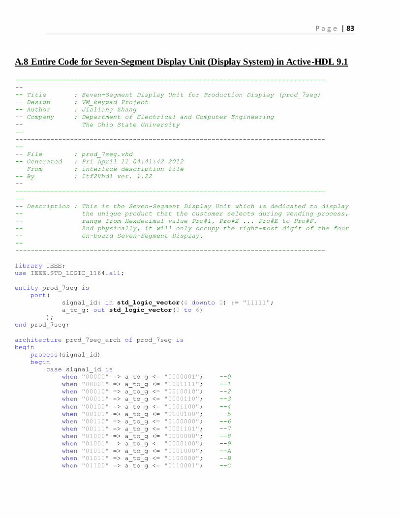
P a g e | 83
A.8 Entire Code for Seven-Segment Display Unit (Display System) in Active-HDL 9.1
-------------------------------------------------------------------------------
--
-- Title : Seven-Segment Display Unit for Production Display (prod_7seg)
-- Design : VM_keypad Project
-- Author : Jialiang Zhang
-- Company : Department of Electrical and Computer Engineering
-- The Ohio State University
--
-------------------------------------------------------------------------------
--
-- File : prod_7seg.vhd
-- Generated : Fri April 11 04:41:42 2012
-- From : interface description file
-- By : Itf2Vhdl ver. 1.22
--
-------------------------------------------------------------------------------
--
-- Description : This is the Seven-Segment Display Unit which is dedicated to display
-- the unique product that the customer selects during vending process,
-- range from Hexdecimal value Pro#1, Pro#2 ... Pro#E to Pro#F.
-- And physically, it will only occupy the right-most digit of the four
-- on-board Seven-Segment Display.
--
-------------------------------------------------------------------------------
library IEEE;
use IEEE.STD_LOGIC_1164.all;
entity prod_7seg is
port(
signal_id: in std_logic_vector(4 downto 0) := "11111";
a_to_g: out std_logic_vector(0 to 6)
);
end prod_7seg;
architecture prod_7seg_arch of prod_7seg is
begin
process(signal_id)
begin
case signal_id is
when "00000" => a_to_g <= "0000001"; --0
when "00001" => a_to_g <= "1001111"; --1
when "00010" => a_to_g <= "0010010"; --2
when "00011" => a_to_g <= "0000110"; --3
when "00100" => a_to_g <= "1001100"; --4
when "00101" => a_to_g <= "0100100"; --5
when "00110" => a_to_g <= "0100000"; --6
when "00111" => a_to_g <= "0001101"; --7
when "01000" => a_to_g <= "0000000"; --8
when "01001" => a_to_g <= "0000100"; --9
when "01010" => a_to_g <= "0001000"; --A
when "01011" => a_to_g <= "1100000"; --B
when "01100" => a_to_g <= "0110001"; --C
P a g e | 84
when "01101" => a_to_g <= "1000010"; --D
when "01110" => a_to_g <= "0110000"; --E
when "01111" => a_to_g <= "0111000"; --F
when "11111" => a_to_g <= "1111110"; --'-'
when others => a_to_g <= "1111110"; --'-'
end case;
end process;
end prod_7seg_arch;
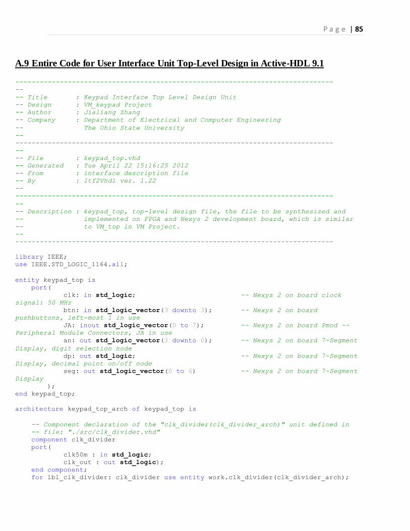
P a g e | 85
A.9 Entire Code for User Interface Unit Top-Level Design in Active-HDL 9.1
-------------------------------------------------------------------------------
--
-- Title : Keypad Interface Top Level Design Unit
-- Design : VM_keypad Project
-- Author : Jialiang Zhang
-- Company : Department of Electrical and Computer Engineering
-- The Ohio State University
--
-------------------------------------------------------------------------------
--
-- File : keypad_top.vhd
-- Generated : Tue April 22 15:16:25 2012
-- From : interface description file
-- By : Itf2Vhdl ver. 1.22
--
-------------------------------------------------------------------------------
--
-- Description : keypad_top, top-level design file, the file to be synthesized and
-- implemented on FPGA and Nexys 2 development board, which is similar
-- to VM_top in VM Project.
--
-------------------------------------------------------------------------------
library IEEE;
use IEEE.STD_LOGIC_1164.all;
entity keypad_top is
port(
clk: in std_logic; -- Nexys 2 on board clock
signal: 50 MHz
btn: in std_logic_vector(3 downto 3); -- Nexys 2 on board
pushbuttons, left-most 1 in use
JA: inout std_logic_vector(0 to 7); -- Nexys 2 on board Pmod --
Peripheral Module Connectors, JA in use
an: out std_logic_vector(3 downto 0); -- Nexys 2 on board 7-Segment
Display, digit selection node
dp: out std_logic; -- Nexys 2 on board 7-Segment
Display, decimal point on/off node
seg: out std_logic_vector(0 to 6) -- Nexys 2 on board 7-Segment
Display
);
end keypad_top;
architecture keypad_top_arch of keypad_top is
-- Component declaration of the "clk_divider(clk_divider_arch)" unit defined in
-- file: "./src/clk_divider.vhd"
component clk_divider
port(
clk50m : in std_logic;
clk_out : out std_logic);
end component;
for lbl_clk_divider: clk_divider use entity work.clk_divider(clk_divider_arch);
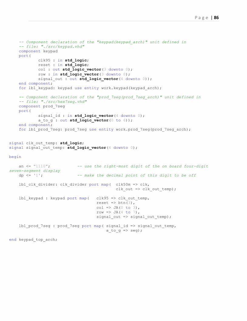
P a g e | 86
-- Component declaration of the "keypad(keypad_arch)" unit defined in
-- file: "./src/keypad.vhd"
component keypad
port(
clk95 : in std_logic;
reset : in std_logic;
col : out std_logic_vector(3 downto 0);
row : in std_logic_vector(3 downto 0);
signal_out : out std_logic_vector(4 downto 0));
end component;
for lbl_keypad: keypad use entity work.keypad(keypad_arch);
-- Component declaration of the "prod_7seg(prod_7seg_arch)" unit defined in
-- file: "./src/hex7seg.vhd"
component prod_7seg
port(
signal_id : in std_logic_vector(4 downto 0);
a_to_g : out std_logic_vector(0 to 6));
end component;
for lbl_prod_7seg: prod_7seg use entity work.prod_7seg(prod_7seg_arch);
signal clk_out_temp: std_logic;
signal signal_out_temp: std_logic_vector(4 downto 0);
begin
an <= "1110"; -- use the right-most digit of the on board four-digit
seven-segment display
dp <= '1'; -- make the decimal point of this digit to be off
lbl_clk_divider: clk_divider port map( clk50m => clk,
clk_out => clk_out_temp);
lbl_keypad : keypad port map( clk95 => clk_out_temp,
reset => btn(3),
col => JA(0 to 3),
row => JA(4 to 7),
signal_out => signal_out_temp);
lbl_prod_7seg : prod_7seg port map( signal_id => signal_out_temp,
a_to_g => seg);
end keypad_top_arch;
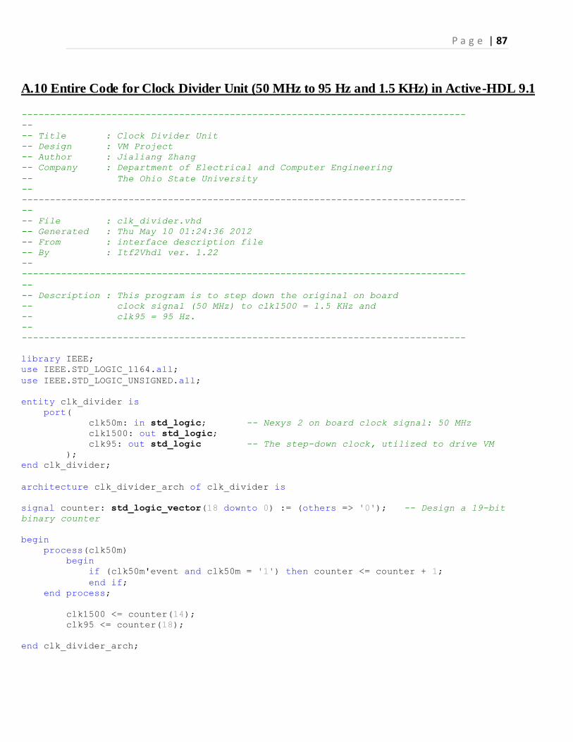
P a g e | 87
A.10 Entire Code for Clock Divider Unit (50 MHz to 95 Hz and 1.5 KHz) in Active-HDL 9.1
-------------------------------------------------------------------------------
--
-- Title : Clock Divider Unit
-- Design : VM Project
-- Author : Jialiang Zhang
-- Company : Department of Electrical and Computer Engineering
-- The Ohio State University
--
-------------------------------------------------------------------------------
--
-- File : clk_divider.vhd
-- Generated : Thu May 10 01:24:36 2012
-- From : interface description file
-- By : Itf2Vhdl ver. 1.22
--
-------------------------------------------------------------------------------
--
-- Description : This program is to step down the original on board
-- clock signal (50 MHz) to clk1500 = 1.5 KHz and
-- clk95 = 95 Hz.
--
-------------------------------------------------------------------------------
library IEEE;
use IEEE.STD_LOGIC_1164.all;
use IEEE.STD_LOGIC_UNSIGNED.all;
entity clk_divider is
port(
clk50m: in std_logic; -- Nexys 2 on board clock signal: 50 MHz
clk1500: out std_logic;
clk95: out std_logic -- The step-down clock, utilized to drive VM
);
end clk_divider;
architecture clk_divider_arch of clk_divider is
signal counter: std_logic_vector(18 downto 0) := (others => '0'); -- Design a 19-bit
binary counter
begin
process(clk50m)
begin
if (clk50m'event and clk50m = '1') then counter <= counter + 1;
end if;
end process;
clk1500 <= counter(14);
clk95 <= counter(18);
end clk_divider_arch;
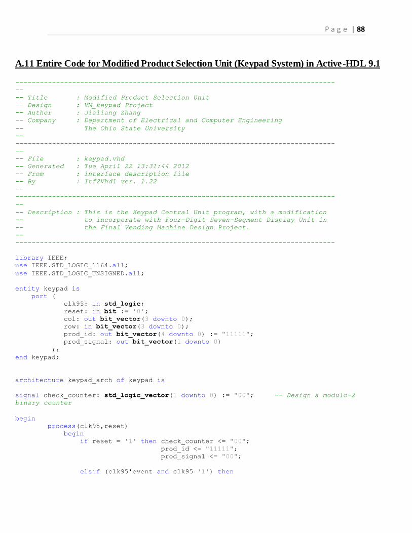
P a g e | 88
A.11 Entire Code for Modified Product Selection Unit (Keypad System) in Active-HDL 9.1
-------------------------------------------------------------------------------
--
-- Title : Modified Product Selection Unit
-- Design : VM_keypad Project
-- Author : Jialiang Zhang
-- Company : Department of Electrical and Computer Engineering
-- The Ohio State University
--
-------------------------------------------------------------------------------
--
-- File : keypad.vhd
-- Generated : Tue April 22 13:31:44 2012
-- From : interface description file
-- By : Itf2Vhdl ver. 1.22
--
-------------------------------------------------------------------------------
--
-- Description : This is the Keypad Central Unit program, with a modification
-- to incorporate with Four-Digit Seven-Segment Display Unit in
-- the Final Vending Machine Design Project.
--
-------------------------------------------------------------------------------
library IEEE;
use IEEE.STD_LOGIC_1164.all;
use IEEE.STD_LOGIC_UNSIGNED.all;
entity keypad is
port (
clk95: in std_logic;
reset: in bit := '0';
col: out bit_vector(3 downto 0);
row: in bit_vector(3 downto 0);
prod_id: out bit_vector(4 downto 0) := "11111";
prod_signal: out bit_vector(1 downto 0)
);
end keypad;
architecture keypad_arch of keypad is
signal check_counter: std_logic_vector(1 downto 0) := "00"; -- Design a modulo-2
binary counter
begin
process(clk95,reset)
begin
if reset = '1' then check_counter <= "00";
prod_id <= "11111";
prod_signal <= "00";
elsif (clk95'event and clk95='1') then
P a g e | 89
case check_counter is
when "00" =>
col <= "1011";
if row = "0111" then prod_id <= "00000"; -- 0
prod_signal <= "01";
elsif row = "1011" then prod_id <= "00100"; -- 4
prod_signal <= "01";
elsif row = "1101" then prod_id <= "01000"; -- 8
prod_signal <= "10";
elsif row = "1110" then prod_id <= "01100"; -- C
prod_signal <= "00";
else null;
end if;
check_counter <= check_counter + 1;
when "01" =>
col <= "1101";
if row = "0111" then prod_id <= "00001"; -- 1
prod_signal <= "01";
elsif row = "1011" then prod_id <= "00101"; -- 5
prod_signal <= "01";
elsif row = "1101" then prod_id <= "01001"; -- 9
prod_signal <= "10";
elsif row = "1110" then prod_id <= "01101"; -- D
prod_signal <= "00";
else null;
end if;
check_counter <= check_counter + 1;
when "10" =>
col <= "1110";
if row = "0111" then prod_id <= "00010"; -- 2
prod_signal <= "01";
elsif row = "1011" then prod_id <= "00110"; -- 6
prod_signal <= "01";
elsif row = "1101" then prod_id <= "01010"; -- A
prod_signal <= "10";
elsif row = "1110" then prod_id <= "01110"; -- E
prod_signal <= "00";
else null;
end if;
check_counter <= check_counter + 1;
when "11" =>
col <= "0111";
if row = "0111" then prod_id <= "00011"; -- 3
prod_signal <= "01";
elsif row = "1011" then prod_id <= "00111"; -- 7
prod_signal <= "01";
elsif row = "1101" then prod_id <= "01011"; -- B
prod_signal <= "10";
elsif row = "1110" then prod_id <= "01111"; -- F
prod_signal <= "00";
else null;
end if;
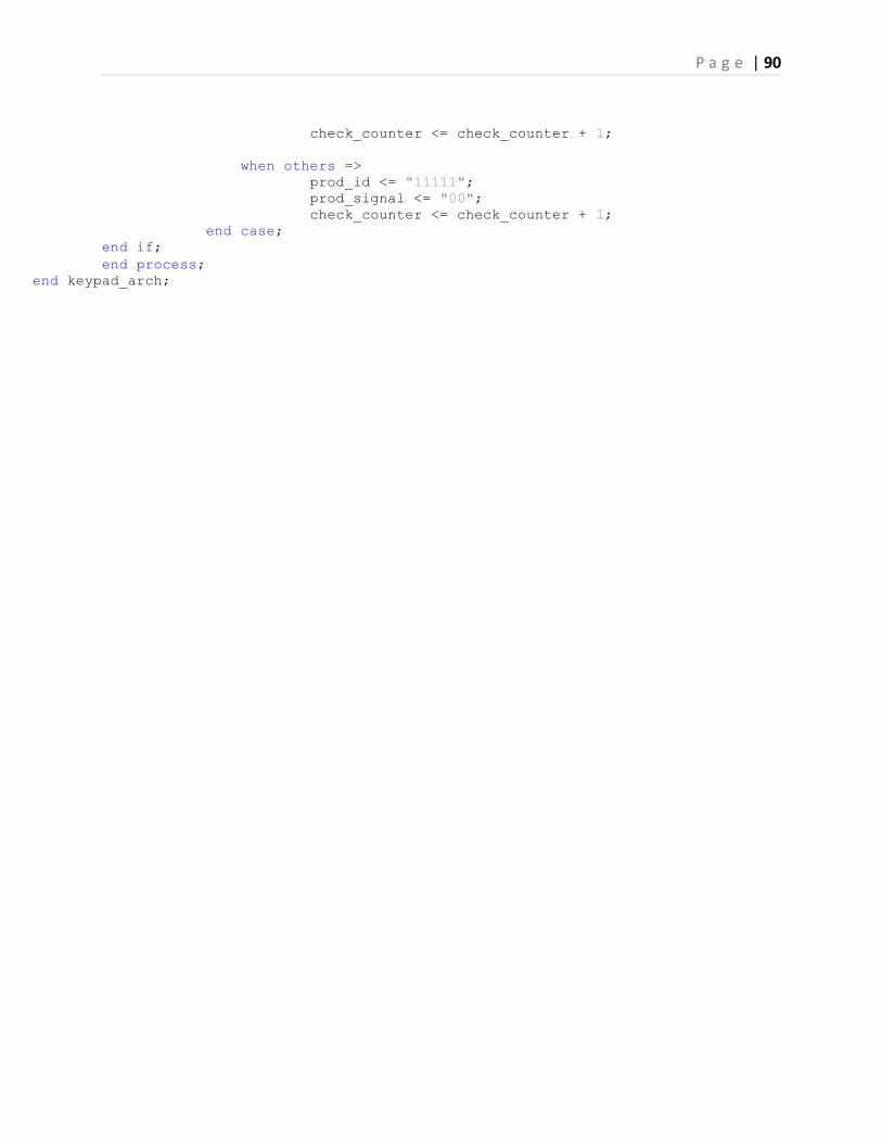
P a g e | 90
check_counter <= check_counter + 1;
when others =>
prod_id <= "11111";
prod_signal <= "00";
check_counter <= check_counter + 1;
end case;
end if;
end process;
end keypad_arch;
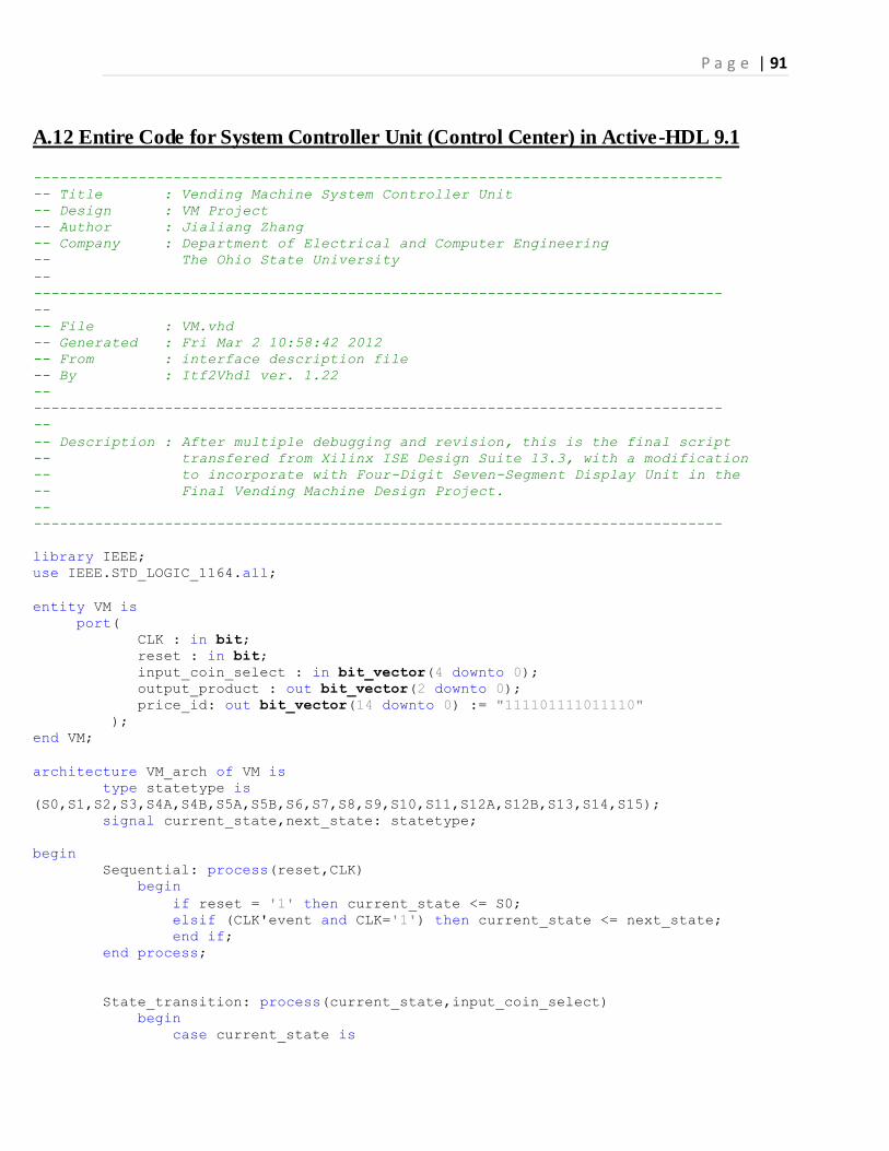
P a g e | 91
A.12 Entire Code for System Controller Unit (Control Center) in Active-HDL 9.1
-------------------------------------------------------------------------------
-- Title : Vending Machine System Controller Unit
-- Design : VM Project
-- Author : Jialiang Zhang
-- Company : Department of Electrical and Computer Engineering
-- The Ohio State University
--
-------------------------------------------------------------------------------
--
-- File : VM.vhd
-- Generated : Fri Mar 2 10:58:42 2012
-- From : interface description file
-- By : Itf2Vhdl ver. 1.22
--
-------------------------------------------------------------------------------
--
-- Description : After multiple debugging and revision, this is the final script
-- transfered from Xilinx ISE Design Suite 13.3, with a modification
-- to incorporate with Four-Digit Seven-Segment Display Unit in the
-- Final Vending Machine Design Project.
--
-------------------------------------------------------------------------------
library IEEE;
use IEEE.STD_LOGIC_1164.all;
entity VM is
port(
CLK : in bit;
reset : in bit;
input_coin_select : in bit_vector(4 downto 0);
output_product : out bit_vector(2 downto 0);
price_id: out bit_vector(14 downto 0) := "111101111011110"
);
end VM;
architecture VM_arch of VM is
type statetype is
(S0,S1,S2,S3,S4A,S4B,S5A,S5B,S6,S7,S8,S9,S10,S11,S12A,S12B,S13,S14,S15);
signal current_state,next_state: statetype;
begin
Sequential: process(reset,CLK)
begin
if reset = '1' then current_state <= S0;
elsif (CLK'event and CLK='1') then current_state <= next_state;
end if;
end process;
State_transition: process(current_state,input_coin_select)
begin
case current_state is
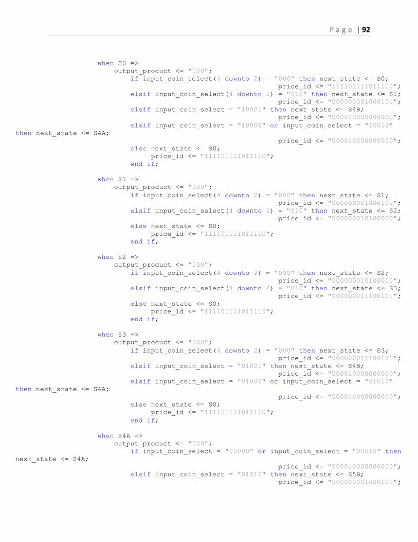
P a g e | 92
when S0 =>
output_product <= "000";
if input_coin_select(4 downto 2) = "000" then next_state <= S0;
price_id <= "111101111011110";
elsif input_coin_select(4 downto 2) = "010" then next_state <= S1;
price_id <= "000000001000101";
elsif input_coin_select = "10001" then next_state <= S4B;
price_id <= "000010000000000";
elsif input_coin_select = "10000" or input_coin_select = "10010"
then next_state <= S4A;
price_id <= "000010000000000";
else next_state <= S0;
price_id <= "111101111011110";
end if;
when S1 =>
output_product <= "000";
if input_coin_select(4 downto 2) = "000" then next_state <= S1;
price_id <= "000000001000101";
elsif input_coin_select(4 downto 2) = "010" then next_state <= S2;
price_id <= "000000010100000";
else next_state <= S0;
price_id <= "111101111011110";
end if;
when S2 =>
output_product <= "000";
if input_coin_select(4 downto 2) = "000" then next_state <= S2;
price_id <= "000000010100000";
elsif input_coin_select(4 downto 2) = "010" then next_state <= S3;
price_id <= "000000011100101";
else next_state <= S0;
price_id <= "111101111011110";
end if;
when S3 =>
output_product <= "000";
if input_coin_select(4 downto 2) = "000" then next_state <= S3;
price_id <= "000000011100101";
elsif input_coin_select = "01001" then next_state <= S4B;
price_id <= "000010000000000";
elsif input_coin_select = "01000" or input_coin_select = "01010"
then next_state <= S4A;
price_id <= "000010000000000";
else next_state <= S0;
price_id <= "111101111011110";
end if;
when S4A =>
output_product <= "000";
if input_coin_select = "00000" or input_coin_select = "00010" then
next_state <= S4A;
price_id <= "000010000000000";
elsif input_coin_select = "01010" then next_state <= S5B;
price_id <= "000010001000101";
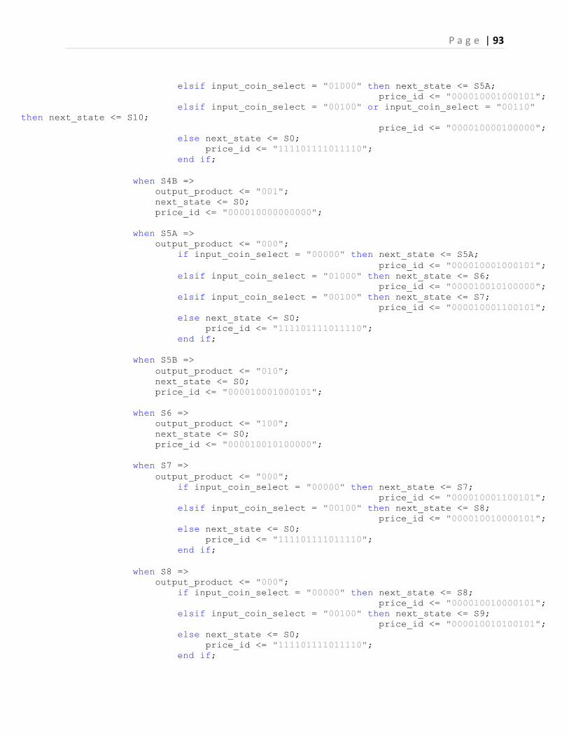
P a g e | 93
elsif input_coin_select = "01000" then next_state <= S5A;
price_id <= "000010001000101";
elsif input_coin_select = "00100" or input_coin_select = "00110"
then next_state <= S10;
price_id <= "000010000100000";
else next_state <= S0;
price_id <= "111101111011110";
end if;
when S4B =>
output_product <= "001";
next_state <= S0;
price_id <= "000010000000000";
when S5A =>
output_product <= "000";
if input_coin_select = "00000" then next_state <= S5A;
price_id <= "000010001000101";
elsif input_coin_select = "01000" then next_state <= S6;
price_id <= "000010010100000";
elsif input_coin_select = "00100" then next_state <= S7;
price_id <= "000010001100101";
else next_state <= S0;
price_id <= "111101111011110";
end if;
when S5B =>
output_product <= "010";
next_state <= S0;
price_id <= "000010001000101";
when S6 =>
output_product <= "100";
next_state <= S0;
price_id <= "000010010100000";
when S7 =>
output_product <= "000";
if input_coin_select = "00000" then next_state <= S7;
price_id <= "000010001100101";
elsif input_coin_select = "00100" then next_state <= S8;
price_id <= "000010010000101";
else next_state <= S0;
price_id <= "111101111011110";
end if;
when S8 =>
output_product <= "000";
if input_coin_select = "00000" then next_state <= S8;
price_id <= "000010010000101";
elsif input_coin_select = "00100" then next_state <= S9;
price_id <= "000010010100101";
else next_state <= S0;
price_id <= "111101111011110";
end if;
P a g e | 94
when S9 =>
output_product <= "100";
next_state <= S0;
price_id <= "000010010100101";
when S10 =>
output_product <= "000";
if input_coin_select = "00000" or input_coin_select = "00010" then
next_state <= S10;
price_id <= "000010000100000";
elsif input_coin_select = "00100" or input_coin_select = "00110"
then next_state <= S11;
price_id <= "000010001000000";
else next_state <= S0;
price_id <= "111101111011110";
end if;
when S11 =>
output_product <= "000";
if input_coin_select = "00000" or input_coin_select = "00010" then
next_state <= S11;
price_id <= "000010001000000";
elsif input_coin_select = "00110" then next_state <= S12B;
price_id <= "000010001100000";
elsif input_coin_select = "00100" then next_state <= S12A;
price_id <= "000010001100000";
elsif input_coin_select = "01000" then next_state <= S8;
price_id <= "000010000100000";
else next_state <= S0;
price_id <= "111101111011110";
end if;
when S12A =>
output_product <= "000";
if input_coin_select = "00000" then next_state <= S12A;
price_id <= "000010001100000";
elsif input_coin_select = "00100" then next_state <= S13;
price_id <= "000010010000000";
elsif input_coin_select = "01000" then next_state <= S9;
price_id <= "000010010100101";
else next_state <= S0;
price_id <= "111101111011110";
end if;
when S12B =>
output_product <= "010";
next_state <= S0;
price_id <= "000010001100000";
when S13 =>
output_product <= "000";
if input_coin_select = "00000" then next_state <= S13;
price_id <= "000010010000000";
elsif input_coin_select = "00100" then next_state <= S14;
P a g e | 95
price_id <= "000010010100000";
elsif input_coin_select = "01000" then next_state <= S15;
price_id <= "000010011000101";
else next_state <= S0;
price_id <= "111101111011110";
end if;
when S14 =>
output_product <= "100";
next_state <= S0;
price_id <= "000010010100000";
when S15 =>
output_product <= "100";
next_state <= S0;
price_id <= "000010011000101";
when others =>
price_id <= "111101111011110";
end case;
end process;
end VM_arch;
P a g e | 96
A.13 Entire Code for Improved Four-Digit Seven-Segment Display Unit in Active-HDL 9.1
-------------------------------------------------------------------------------
--
-- Title : Improved Four-Digit Seven-Segment Display Unit for
-- Price Indication and Product Display (fourdigit_7seg)
-- Design : Machine Project
-- Author : Jialiang Zhang
-- Company : Department of Electrical and Computer Engineering
-- The Ohio State University
--
-------------------------------------------------------------------------------
--
-- File : fourdigit_7seg.vhd
-- Generated : Fri April 11 04:41:42 2012
-- From : interface description file
-- By : Itf2Vhdl ver. 1.22
--
-------------------------------------------------------------------------------
--
-- Description : This is the Improved Four-Digit Seven-Segment Display Unit for
-- Price Indication and Product Display, which serves two roles --
-- dedicated to display the unique product that the customer selects
-- during vending process, range from Hexadecimal value Pro#1, Pro#2,
-- Pro#3, ... Pro#E to Pro#F, and locates only on the right-most
-- digit of the four on-board Seven-Segment Display; and to display
-- the actual amount of money/coins inserted dynamically, which
-- locates on the first three digits of the four on-board Seven-
-- Segment Display. For example: 1.55 indicates the machine accepted
-- one dollar and fifty-five cents all ready.
--
-------------------------------------------------------------------------------
library IEEE;
use IEEE.STD_LOGIC_1164.all;
use IEEE.STD_LOGIC_UNSIGNED.all;
entity fourdigit_7seg is
port(
clk1500: in std_logic;
prod_id: in bit_vector(4 downto 0) := "11111";
price_id: in bit_vector(14 downto 0) := "111101111011110";
a_to_g: out bit_vector(0 to 6);
an_temp: out bit_vector(3 downto 0);
dp_temp: out bit
);
end fourdigit_7seg;
architecture fourdigit_7seg_arch of fourdigit_7seg is
signal counter: std_logic_vector(1 downto 0);
signal test_id: bit_vector(4 downto 0);
signal aen: bit_vector(3 downto 0);
begin
P a g e | 97
process(clk1500)
begin
if (clk1500'event and clk1500 = '1') then counter <= counter + 1;
end if;
end process;
process(counter,prod_id,price_id)
begin
case counter is
when "00" => test_id <= prod_id;
when "01" => test_id <= price_id(4 downto 0);
when "10" => test_id <= price_id(9 downto 5);
when others => test_id <= price_id(14 downto 10);
end case;
end process;
process(test_id)
begin
case test_id is
when "00000" => a_to_g <= "0000001"; -- 0
when "00001" => a_to_g <= "1001111"; -- 1
when "00010" => a_to_g <= "0010010"; -- 2
when "00011" => a_to_g <= "0000110"; -- 3
when "00100" => a_to_g <= "1001100"; -- 4
when "00101" => a_to_g <= "0100100"; -- 5
when "00110" => a_to_g <= "0100000"; -- 6
when "00111" => a_to_g <= "0001101"; -- 7
when "01000" => a_to_g <= "0000000"; -- 8
when "01001" => a_to_g <= "0000100"; -- 9
when "01010" => a_to_g <= "0001000"; -- A
when "01011" => a_to_g <= "1100000"; -- B
when "01100" => a_to_g <= "0110001"; -- C
when "01101" => a_to_g <= "1000010"; -- D
when "01110" => a_to_g <= "0110000"; -- E
when "01111" => a_to_g <= "0111000"; -- F
-- Define two corner cases: string"---" and "=" on 7-seg display
when "11110" => a_to_g <= "1111110"; -- Initial display for price, as "-"
when "11111" => a_to_g <= "0110111"; -- Initial display for product, as "="
when others => a_to_g <= "1001000";
end case;
end process;
aen <= "1111";
process(counter,aen)
begin
an_temp <= aen;
-- Flash each bit of the 4-digit 7-seg display with updated value, adapted from R.
-- Haskell and D. Hanna’s book Digital Design Using Digilent FPGA Boards.
if aen(conv_integer(counter)) = '1' then
an_temp(conv_integer(counter)) <= '0';
end if;
P a g e | 98
-- Flash each decimal point of the 4-digit 7-seg display, but only the
-- left-most decimal point will be display explicitly, for example, 1.55
if counter = "11" then
dp_temp <= '0';
else dp_temp <= '1';
end if;
end process;
end fourdigit_7seg_arch;
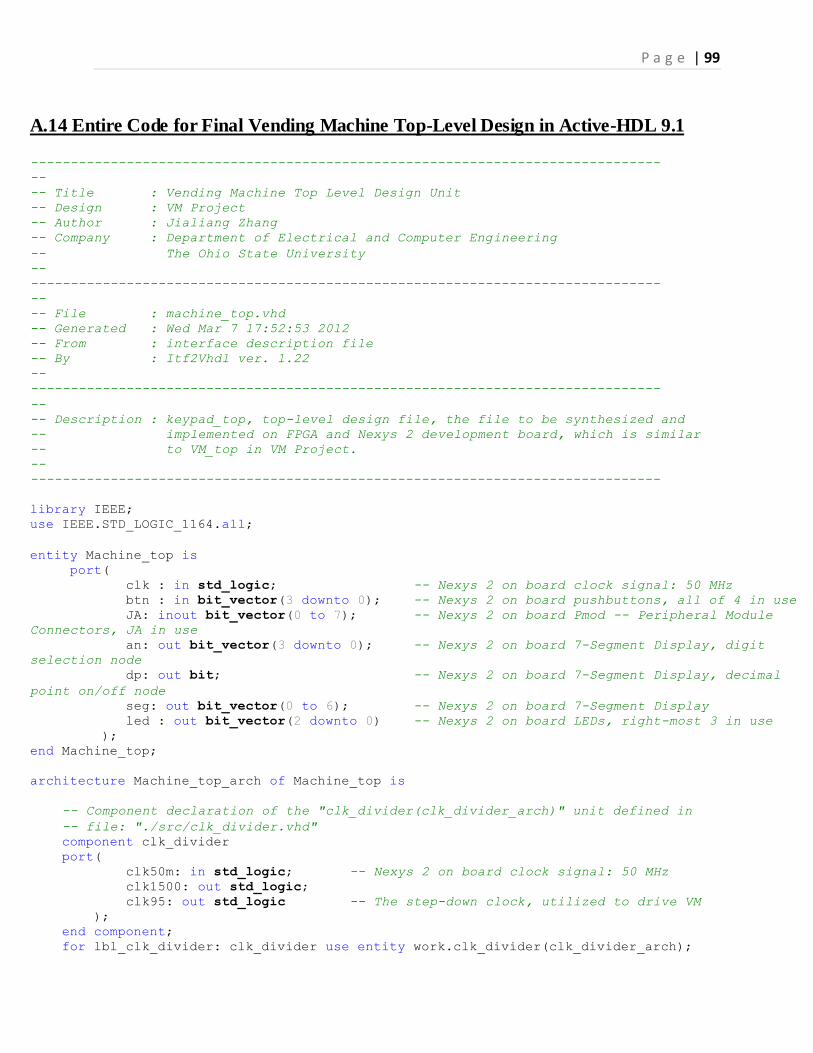
P a g e | 99
A.14 Entire Code for Final Vending Machine Top-Level Design in Active-HDL 9.1
-------------------------------------------------------------------------------
--
-- Title : Vending Machine Top Level Design Unit
-- Design : VM Project
-- Author : Jialiang Zhang
-- Company : Department of Electrical and Computer Engineering
-- The Ohio State University
--
-------------------------------------------------------------------------------
--
-- File : machine_top.vhd
-- Generated : Wed Mar 7 17:52:53 2012
-- From : interface description file
-- By : Itf2Vhdl ver. 1.22
--
-------------------------------------------------------------------------------
--
-- Description : keypad_top, top-level design file, the file to be synthesized and
-- implemented on FPGA and Nexys 2 development board, which is similar
-- to VM_top in VM Project.
--
-------------------------------------------------------------------------------
library IEEE;
use IEEE.STD_LOGIC_1164.all;
entity Machine_top is
port(
clk : in std_logic; -- Nexys 2 on board clock signal: 50 MHz
btn : in bit_vector(3 downto 0); -- Nexys 2 on board pushbuttons, all of 4 in use
JA: inout bit_vector(0 to 7); -- Nexys 2 on board Pmod -- Peripheral Module
Connectors, JA in use
an: out bit_vector(3 downto 0); -- Nexys 2 on board 7-Segment Display, digit
selection node
dp: out bit; -- Nexys 2 on board 7-Segment Display, decimal
point on/off node
seg: out bit_vector(0 to 6); -- Nexys 2 on board 7-Segment Display
led : out bit_vector(2 downto 0) -- Nexys 2 on board LEDs, right-most 3 in use
);
end Machine_top;
architecture Machine_top_arch of Machine_top is
-- Component declaration of the "clk_divider(clk_divider_arch)" unit defined in
-- file: "./src/clk_divider.vhd"
component clk_divider
port(
clk50m: in std_logic; -- Nexys 2 on board clock signal: 50 MHz
clk1500: out std_logic;
clk95: out std_logic -- The step-down clock, utilized to drive VM
);
end component;
for lbl_clk_divider: clk_divider use entity work.clk_divider(clk_divider_arch);
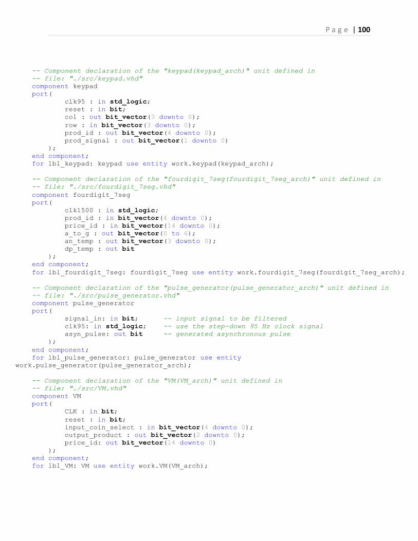
P a g e | 100
-- Component declaration of the "keypad(keypad_arch)" unit defined in
-- file: "./src/keypad.vhd"
component keypad
port(
clk95 : in std_logic;
reset : in bit;
col : out bit_vector(3 downto 0);
row : in bit_vector(3 downto 0);
prod_id : out bit_vector(4 downto 0);
prod_signal : out bit_vector(1 downto 0)
);
end component;
for lbl_keypad: keypad use entity work.keypad(keypad_arch);
-- Component declaration of the "fourdigit_7seg(fourdigit_7seg_arch)" unit defined in
-- file: "./src/fourdigit_7seg.vhd"
component fourdigit_7seg
port(
clk1500 : in std_logic;
prod_id : in bit_vector(4 downto 0);
price_id : in bit_vector(14 downto 0);
a_to_g : out bit_vector(0 to 6);
an_temp : out bit_vector(3 downto 0);
dp_temp : out bit
);
end component;
for lbl_fourdigit_7seg: fourdigit_7seg use entity work.fourdigit_7seg(fourdigit_7seg_arch);
-- Component declaration of the "pulse_generator(pulse_generator_arch)" unit defined in
-- file: "./src/pulse_generator.vhd"
component pulse_generator
port(
signal_in: in bit; -- input signal to be filtered
clk95: in std_logic; -- use the step-down 95 Hz clock signal
asyn_pulse: out bit -- generated asynchronous pulse
);
end component;
for lbl_pulse_generator: pulse_generator use entity
work.pulse_generator(pulse_generator_arch);
-- Component declaration of the "VM(VM_arch)" unit defined in
-- file: "./src/VM.vhd"
component VM
port(
CLK : in bit;
reset : in bit;
input_coin_select : in bit_vector(4 downto 0);
output_product : out bit_vector(2 downto 0);
price_id: out bit_vector(14 downto 0)
);
end component;
for lbl_VM: VM use entity work.VM(VM_arch);
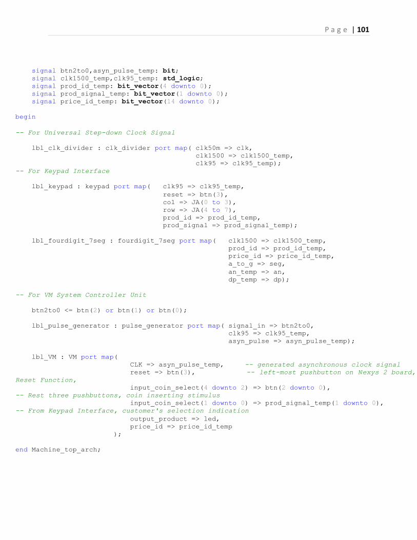
P a g e | 101
signal btn2to0,asyn_pulse_temp: bit;
signal clk1500_temp,clk95_temp: std_logic;
signal prod_id_temp: bit_vector(4 downto 0);
signal prod_signal_temp: bit_vector(1 downto 0);
signal price_id_temp: bit_vector(14 downto 0);
begin
-- For Universal Step-down Clock Signal
lbl_clk_divider : clk_divider port map( clk50m => clk,
clk1500 => clk1500_temp,
clk95 => clk95_temp);
-- For Keypad Interface
lbl_keypad : keypad port map( clk95 => clk95_temp,
reset => btn(3),
col => JA(0 to 3),
row => JA(4 to 7),
prod_id => prod_id_temp,
prod_signal => prod_signal_temp);
lbl_fourdigit_7seg : fourdigit_7seg port map( clk1500 => clk1500_temp,
prod_id => prod_id_temp,
price_id => price_id_temp,
a_to_g => seg,
an_temp => an,
dp_temp => dp);
-- For VM System Controller Unit
btn2to0 <= btn(2) or btn(1) or btn(0);
lbl_pulse_generator : pulse_generator port map( signal_in => btn2to0,
clk95 => clk95_temp,
asyn_pulse => asyn_pulse_temp);
lbl_VM : VM port map(
CLK => asyn_pulse_temp, -- generated asynchronous clock signal
reset => btn(3), -- left-most pushbutton on Nexys 2 board,
Reset Function,
input_coin_select(4 downto 2) => btn(2 downto 0),
-- Rest three pushbuttons, coin inserting stimulus
input_coin_select(1 downto 0) => prod_signal_temp(1 downto 0),
-- From Keypad Interface, customer's selection indication
output_product => led,
price_id => price_id_temp
);
end Machine_top_arch;
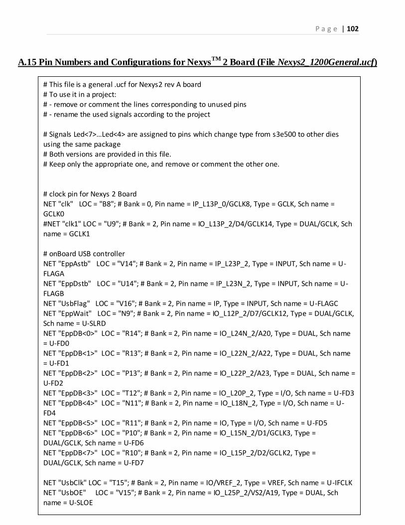
P a g e | 102
A.15 Pin Numbers and Configurations for NexysTM
2 Board (File Nexys2_1200General.ucf)
# This file is a general .ucf for Nexys2 rev A board
# To use it in a project: # - remove or comment the lines corresponding to unused pins
# - rename the used signals according to the project
# Signals Led<7>…Led<4> are assigned to pins which change type from s3e500 to other dies using the same package
# Both versions are provided in this file. # Keep only the appropriate one, and remove or comment the other one.
# clock pin for Nexys 2 Board
NET "clk" LOC = "B8"; # Bank = 0, Pin name = IP_L13P_0/GCLK8, Type = GCLK, Sch name = GCLK0
#NET "clk1" LOC = "U9"; # Bank = 2, Pin name = IO_L13P_2/D4/GCLK14, Type = DUAL/GCLK, Sch name = GCLK1
# onBoard USB controller NET "EppAstb" LOC = "V14"; # Bank = 2, Pin name = IP_L23P_2, Type = INPUT, Sch name = U-
FLAGA NET "EppDstb" LOC = "U14"; # Bank = 2, Pin name = IP_L23N_2, Type = INPUT, Sch name = U-
FLAGB NET "UsbFlag" LOC = "V16"; # Bank = 2, Pin name = IP, Type = INPUT, Sch name = U-FLAGC
NET "EppWait" LOC = "N9"; # Bank = 2, Pin name = IO_L12P_2/D7/GCLK12, Type = DUAL/GCLK, Sch name = U-SLRD
NET "EppDB<0>" LOC = "R14"; # Bank = 2, Pin name = IO_L24N_2/A20, Type = DUAL, Sch name
= U-FD0 NET "EppDB<1>" LOC = "R13"; # Bank = 2, Pin name = IO_L22N_2/A22, Type = DUAL, Sch name
= U-FD1 NET "EppDB<2>" LOC = "P13"; # Bank = 2, Pin name = IO_L22P_2/A23, Type = DUAL, Sch name =
U-FD2 NET "EppDB<3>" LOC = "T12"; # Bank = 2, Pin name = IO_L20P_2, Type = I/O, Sch name = U-FD3
NET "EppDB<4>" LOC = "N11"; # Bank = 2, Pin name = IO_L18N_2, Type = I/O, Sch name = U-
FD4 NET "EppDB<5>" LOC = "R11"; # Bank = 2, Pin name = IO, Type = I/O, Sch name = U-FD5
NET "EppDB<6>" LOC = "P10"; # Bank = 2, Pin name = IO_L15N_2/D1/GCLK3, Type =
DUAL/GCLK, Sch name = U-FD6
NET "EppDB<7>" LOC = "R10"; # Bank = 2, Pin name = IO_L15P_2/D2/GCLK2, Type = DUAL/GCLK, Sch name = U-FD7
NET "UsbClk" LOC = "T15"; # Bank = 2, Pin name = IO/VREF_2, Type = VREF, Sch name = U-IFCLK NET "UsbOE" LOC = "V15"; # Bank = 2, Pin name = IO_L25P_2/VS2/A19, Type = DUAL, Sch
name = U-SLOE
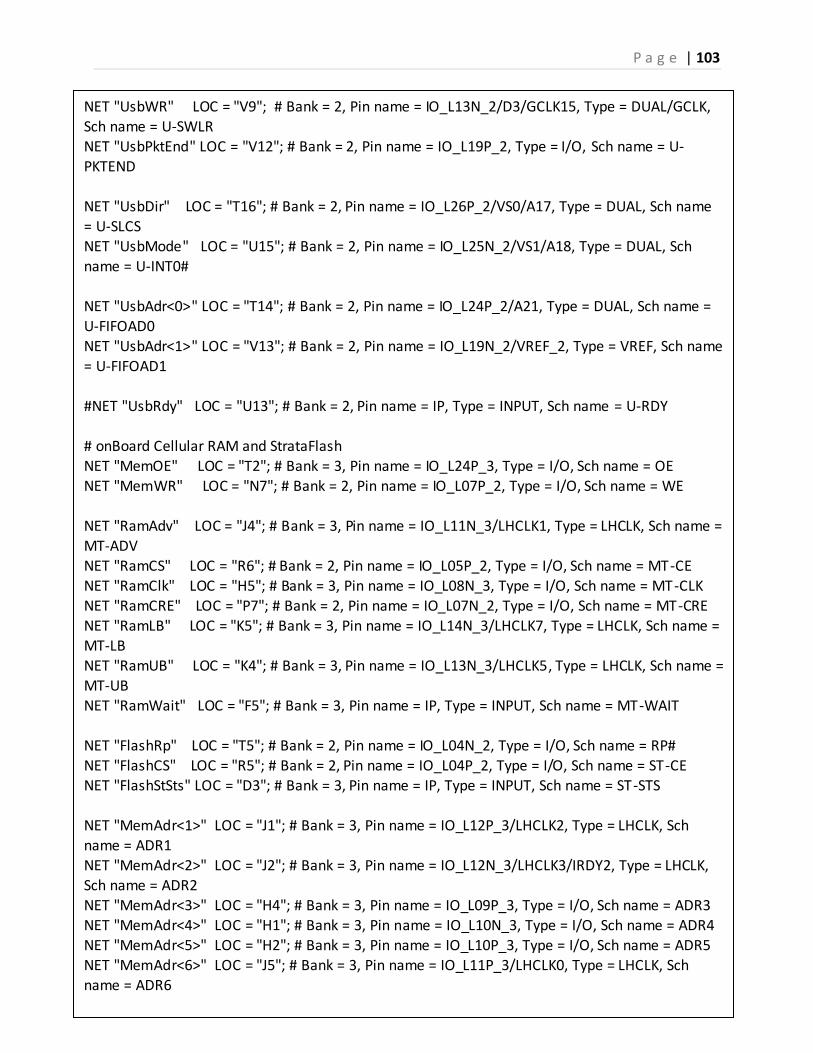
P a g e | 103
NET "UsbWR" LOC = "V9"; # Bank = 2, Pin name = IO_L13N_2/D3/GCLK15, Type = DUAL/GCLK,
Sch name = U-SWLR NET "UsbPktEnd" LOC = "V12"; # Bank = 2, Pin name = IO_L19P_2, Type = I/O, Sch name = U-
PKTEND
NET "UsbDir" LOC = "T16"; # Bank = 2, Pin name = IO_L26P_2/VS0/A17, Type = DUAL, Sch name
= U-SLCS NET "UsbMode" LOC = "U15"; # Bank = 2, Pin name = IO_L25N_2/VS1/A18, Type = DUAL, Sch
name = U-INT0#
NET "UsbAdr<0>" LOC = "T14"; # Bank = 2, Pin name = IO_L24P_2/A21, Type = DUAL, Sch name = U-FIFOAD0
NET "UsbAdr<1>" LOC = "V13"; # Bank = 2, Pin name = IO_L19N_2/VREF_2, Type = VREF, Sch name
= U-FIFOAD1
#NET "UsbRdy" LOC = "U13"; # Bank = 2, Pin name = IP, Type = INPUT, Sch name = U-RDY
# onBoard Cellular RAM and StrataFlash NET "MemOE" LOC = "T2"; # Bank = 3, Pin name = IO_L24P_3, Type = I/O, Sch name = OE
NET "MemWR" LOC = "N7"; # Bank = 2, Pin name = IO_L07P_2, Type = I/O, Sch name = WE
NET "RamAdv" LOC = "J4"; # Bank = 3, Pin name = IO_L11N_3/LHCLK1, Type = LHCLK, Sch name =
MT-ADV NET "RamCS" LOC = "R6"; # Bank = 2, Pin name = IO_L05P_2, Type = I/O, Sch name = MT-CE
NET "RamClk" LOC = "H5"; # Bank = 3, Pin name = IO_L08N_3, Type = I/O, Sch name = MT-CLK NET "RamCRE" LOC = "P7"; # Bank = 2, Pin name = IO_L07N_2, Type = I/O, Sch name = MT-CRE
NET "RamLB" LOC = "K5"; # Bank = 3, Pin name = IO_L14N_3/LHCLK7, Type = LHCLK, Sch name = MT-LB
NET "RamUB" LOC = "K4"; # Bank = 3, Pin name = IO_L13N_3/LHCLK5, Type = LHCLK, Sch name =
MT-UB NET "RamWait" LOC = "F5"; # Bank = 3, Pin name = IP, Type = INPUT, Sch name = MT-WAIT
NET "FlashRp" LOC = "T5"; # Bank = 2, Pin name = IO_L04N_2, Type = I/O, Sch name = RP#
NET "FlashCS" LOC = "R5"; # Bank = 2, Pin name = IO_L04P_2, Type = I/O, Sch name = ST-CE NET "FlashStSts" LOC = "D3"; # Bank = 3, Pin name = IP, Type = INPUT, Sch name = ST-STS
NET "MemAdr<1>" LOC = "J1"; # Bank = 3, Pin name = IO_L12P_3/LHCLK2, Type = LHCLK, Sch
name = ADR1
NET "MemAdr<2>" LOC = "J2"; # Bank = 3, Pin name = IO_L12N_3/LHCLK3/IRDY2, Type = LHCLK,
Sch name = ADR2
NET "MemAdr<3>" LOC = "H4"; # Bank = 3, Pin name = IO_L09P_3, Type = I/O, Sch name = ADR3 NET "MemAdr<4>" LOC = "H1"; # Bank = 3, Pin name = IO_L10N_3, Type = I/O, Sch name = ADR4
NET "MemAdr<5>" LOC = "H2"; # Bank = 3, Pin name = IO_L10P_3, Type = I/O, Sch name = ADR5 NET "MemAdr<6>" LOC = "J5"; # Bank = 3, Pin name = IO_L11P_3/LHCLK0, Type = LHCLK, Sch
name = ADR6
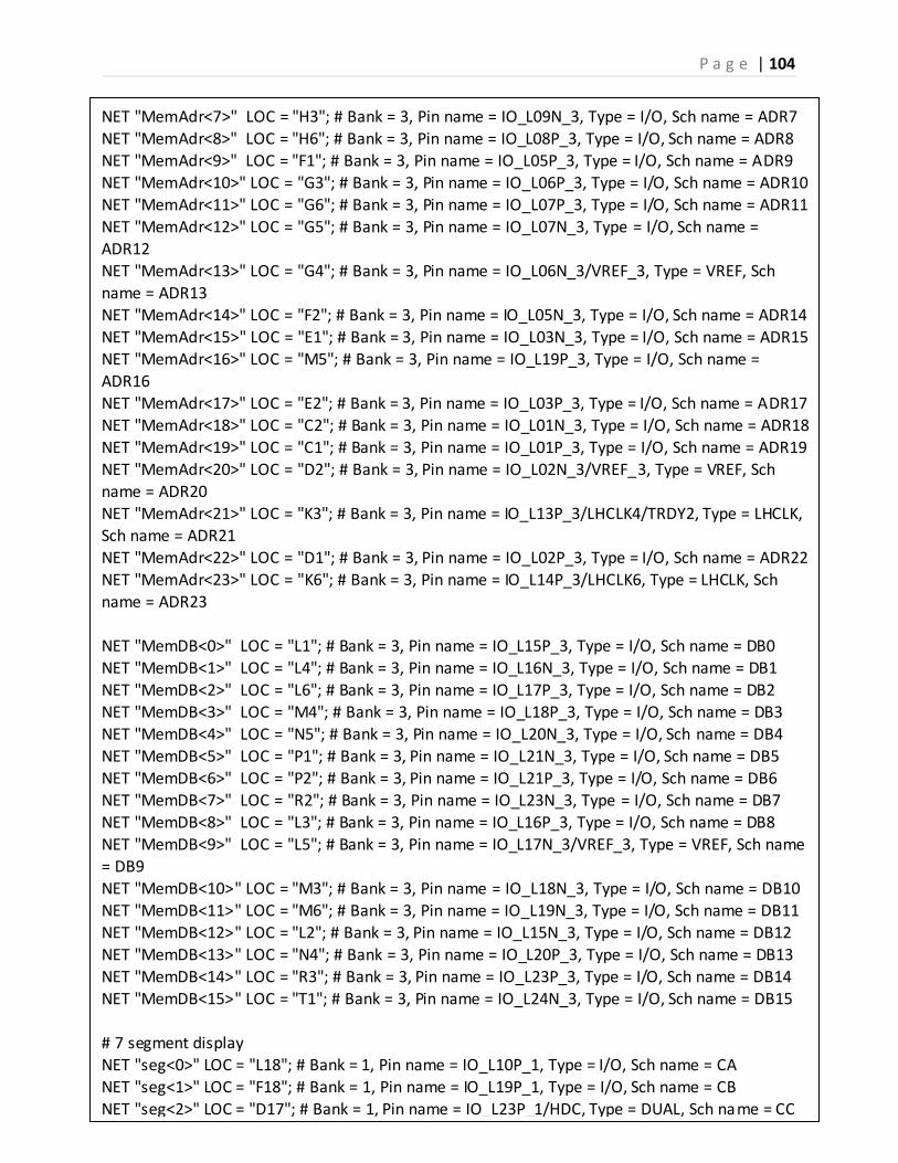
P a g e | 104
NET "MemAdr<7>" LOC = "H3"; # Bank = 3, Pin name = IO_L09N_3, Type = I/O, Sch name = ADR7
NET "MemAdr<8>" LOC = "H6"; # Bank = 3, Pin name = IO_L08P_3, Type = I/O, Sch name = ADR8 NET "MemAdr<9>" LOC = "F1"; # Bank = 3, Pin name = IO_L05P_3, Type = I/O, Sch name = ADR9
NET "MemAdr<10>" LOC = "G3"; # Bank = 3, Pin name = IO_L06P_3, Type = I/O, Sch name = ADR10 NET "MemAdr<11>" LOC = "G6"; # Bank = 3, Pin name = IO_L07P_3, Type = I/O, Sch name = ADR11
NET "MemAdr<12>" LOC = "G5"; # Bank = 3, Pin name = IO_L07N_3, Type = I/O, Sch name =
ADR12 NET "MemAdr<13>" LOC = "G4"; # Bank = 3, Pin name = IO_L06N_3/VREF_3, Type = VREF, Sch
name = ADR13 NET "MemAdr<14>" LOC = "F2"; # Bank = 3, Pin name = IO_L05N_3, Type = I/O, Sch name = ADR14
NET "MemAdr<15>" LOC = "E1"; # Bank = 3, Pin name = IO_L03N_3, Type = I/O, Sch name = ADR15 NET "MemAdr<16>" LOC = "M5"; # Bank = 3, Pin name = IO_L19P_3, Type = I/O, Sch name =
ADR16 NET "MemAdr<17>" LOC = "E2"; # Bank = 3, Pin name = IO_L03P_3, Type = I/O, Sch name = ADR17
NET "MemAdr<18>" LOC = "C2"; # Bank = 3, Pin name = IO_L01N_3, Type = I/O, Sch name = ADR18
NET "MemAdr<19>" LOC = "C1"; # Bank = 3, Pin name = IO_L01P_3, Type = I/O, Sch name = ADR19 NET "MemAdr<20>" LOC = "D2"; # Bank = 3, Pin name = IO_L02N_3/VREF_3, Type = VREF, Sch
name = ADR20 NET "MemAdr<21>" LOC = "K3"; # Bank = 3, Pin name = IO_L13P_3/LHCLK4/TRDY2, Type = LHCLK,
Sch name = ADR21 NET "MemAdr<22>" LOC = "D1"; # Bank = 3, Pin name = IO_L02P_3, Type = I/O, Sch name = ADR22
NET "MemAdr<23>" LOC = "K6"; # Bank = 3, Pin name = IO_L14P_3/LHCLK6, Type = LHCLK, Sch
name = ADR23
NET "MemDB<0>" LOC = "L1"; # Bank = 3, Pin name = IO_L15P_3, Type = I/O, Sch name = DB0 NET "MemDB<1>" LOC = "L4"; # Bank = 3, Pin name = IO_L16N_3, Type = I/O, Sch name = DB1
NET "MemDB<2>" LOC = "L6"; # Bank = 3, Pin name = IO_L17P_3, Type = I/O, Sch name = DB2 NET "MemDB<3>" LOC = "M4"; # Bank = 3, Pin name = IO_L18P_3, Type = I/O, Sch name = DB3
NET "MemDB<4>" LOC = "N5"; # Bank = 3, Pin name = IO_L20N_3, Type = I/O, Sch name = DB4
NET "MemDB<5>" LOC = "P1"; # Bank = 3, Pin name = IO_L21N_3, Type = I/O, Sch name = DB5 NET "MemDB<6>" LOC = "P2"; # Bank = 3, Pin name = IO_L21P_3, Type = I/O, Sch name = DB6
NET "MemDB<7>" LOC = "R2"; # Bank = 3, Pin name = IO_L23N_3, Type = I/O, Sch name = DB7 NET "MemDB<8>" LOC = "L3"; # Bank = 3, Pin name = IO_L16P_3, Type = I/O, Sch name = DB8
NET "MemDB<9>" LOC = "L5"; # Bank = 3, Pin name = IO_L17N_3/VREF_3, Type = VREF, Sch name = DB9
NET "MemDB<10>" LOC = "M3"; # Bank = 3, Pin name = IO_L18N_3, Type = I/O, Sch name = DB10 NET "MemDB<11>" LOC = "M6"; # Bank = 3, Pin name = IO_L19N_3, Type = I/O, Sch name = DB11
NET "MemDB<12>" LOC = "L2"; # Bank = 3, Pin name = IO_L15N_3, Type = I/O, Sch name = DB12
NET "MemDB<13>" LOC = "N4"; # Bank = 3, Pin name = IO_L20P_3, Type = I/O, Sch name = DB13
NET "MemDB<14>" LOC = "R3"; # Bank = 3, Pin name = IO_L23P_3, Type = I/O, Sch name = DB14
NET "MemDB<15>" LOC = "T1"; # Bank = 3, Pin name = IO_L24N_3, Type = I/O, Sch name = DB15
# 7 segment display NET "seg<0>" LOC = "L18"; # Bank = 1, Pin name = IO_L10P_1, Type = I/O, Sch name = CA
NET "seg<1>" LOC = "F18"; # Bank = 1, Pin name = IO_L19P_1, Type = I/O, Sch name = CB
NET "seg<2>" LOC = "D17"; # Bank = 1, Pin name = IO_L23P_1/HDC, Type = DUAL, Sch name = CC
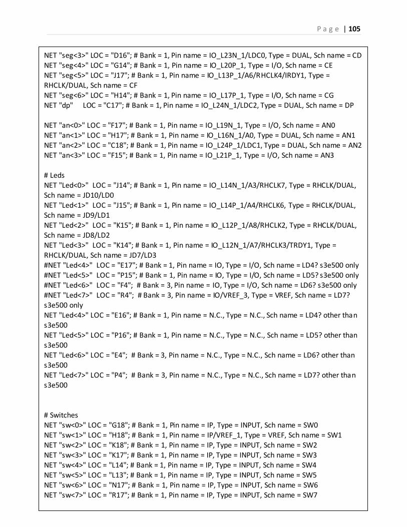
P a g e | 105
NET "seg<3>" LOC = "D16"; # Bank = 1, Pin name = IO_L23N_1/LDC0, Type = DUAL, Sch name = CD
NET "seg<4>" LOC = "G14"; # Bank = 1, Pin name = IO_L20P_1, Type = I/O, Sch name = CE NET "seg<5>" LOC = "J17"; # Bank = 1, Pin name = IO_L13P_1/A6/RHCLK4/IRDY1, Type =
RHCLK/DUAL, Sch name = CF
NET "seg<6>" LOC = "H14"; # Bank = 1, Pin name = IO_L17P_1, Type = I/O, Sch name = CG NET "dp" LOC = "C17"; # Bank = 1, Pin name = IO_L24N_1/LDC2, Type = DUAL, Sch name = DP
NET "an<0>" LOC = "F17"; # Bank = 1, Pin name = IO_L19N_1, Type = I/O, Sch name = AN0
NET "an<1>" LOC = "H17"; # Bank = 1, Pin name = IO_L16N_1/A0, Type = DUAL, Sch name = AN1 NET "an<2>" LOC = "C18"; # Bank = 1, Pin name = IO_L24P_1/LDC1, Type = DUAL, Sch name = AN2
NET "an<3>" LOC = "F15"; # Bank = 1, Pin name = IO_L21P_1, Type = I/O, Sch name = AN3
# Leds
NET "Led<0>" LOC = "J14"; # Bank = 1, Pin name = IO_L14N_1/A3/RHCLK7, Type = RHCLK/DUAL, Sch name = JD10/LD0
NET "Led<1>" LOC = "J15"; # Bank = 1, Pin name = IO_L14P_1/A4/RHCLK6, Type = RHCLK/DUAL, Sch name = JD9/LD1
NET "Led<2>" LOC = "K15"; # Bank = 1, Pin name = IO_L12P_1/A8/RHCLK2, Type = RHCLK/DUAL, Sch name = JD8/LD2
NET "Led<3>" LOC = "K14"; # Bank = 1, Pin name = IO_L12N_1/A7/RHCLK3/TRDY1, Type =
RHCLK/DUAL, Sch name = JD7/LD3 #NET "Led<4>" LOC = "E17"; # Bank = 1, Pin name = IO, Type = I/O, Sch name = LD4? s3e500 only
#NET "Led<5>" LOC = "P15"; # Bank = 1, Pin name = IO, Type = I/O, Sch name = LD5? s3e500 only #NET "Led<6>" LOC = "F4"; # Bank = 3, Pin name = IO, Type = I/O, Sch name = LD6? s3e500 only
#NET "Led<7>" LOC = "R4"; # Bank = 3, Pin name = IO/VREF_3, Type = VREF, Sch name = LD7? s3e500 only
NET "Led<4>" LOC = "E16"; # Bank = 1, Pin name = N.C., Type = N.C., Sch name = LD4? other than
s3e500 NET "Led<5>" LOC = "P16"; # Bank = 1, Pin name = N.C., Type = N.C., Sch name = LD5? other than
s3e500 NET "Led<6>" LOC = "E4"; # Bank = 3, Pin name = N.C., Type = N.C., Sch name = LD6? other than
s3e500 NET "Led<7>" LOC = "P4"; # Bank = 3, Pin name = N.C., Type = N.C., Sch name = LD7? other than
s3e500
# Switches NET "sw<0>" LOC = "G18"; # Bank = 1, Pin name = IP, Type = INPUT, Sch name = SW0
NET "sw<1>" LOC = "H18"; # Bank = 1, Pin name = IP/VREF_1, Type = VREF, Sch name = SW1
NET "sw<2>" LOC = "K18"; # Bank = 1, Pin name = IP, Type = INPUT, Sch name = SW2
NET "sw<3>" LOC = "K17"; # Bank = 1, Pin name = IP, Type = INPUT, Sch name = SW3 NET "sw<4>" LOC = "L14"; # Bank = 1, Pin name = IP, Type = INPUT, Sch name = SW4
NET "sw<5>" LOC = "L13"; # Bank = 1, Pin name = IP, Type = INPUT, Sch name = SW5
NET "sw<6>" LOC = "N17"; # Bank = 1, Pin name = IP, Type = INPUT, Sch name = SW6 NET "sw<7>" LOC = "R17"; # Bank = 1, Pin name = IP, Type = INPUT, Sch name = SW7
P a g e | 106
# Buttons
NET "btn<0>" LOC = "B18"; # Bank = 1, Pin name = IP, Type = INPUT, Sch name = BTN0 NET "btn<1>" LOC = "D18"; # Bank = 1, Pin name = IP/VREF_1, Type = VREF, Sch name = BTN1
NET "btn<2>" LOC = "E18"; # Bank = 1, Pin name = IP, Type = INPUT, Sch name = BTN2
NET "btn<3>" LOC = "H13"; # Bank = 1, Pin name = IP, Type = INPUT, Sch name = BTN3
# VGA Connector NET "vgaRed<1>" LOC = "R9"; # Bank = 2, Pin name = IO/D5, Type = DUAL, Sch name = RED0
NET "vgaRed<2>" LOC = "T8"; # Bank = 2, Pin name = IO_L10N_2, Type = I/O, Sch name = RED1 NET "vgaRed<3>" LOC = "R8"; # Bank = 2, Pin name = IO_L10P_2, Type = I/O, Sch name = RED2
NET "vgaGreen<1>" LOC = "N8"; # Bank = 2, Pin name = IO_L09N_2, Type = I/O, Sch name = GRN0
NET "vgaGreen<2>" LOC = "P8"; # Bank = 2, Pin name = IO_L09P_2, Type = I/O, Sch name = GRN1 NET "vgaGreen<3>" LOC = "P6"; # Bank = 2, Pin name = IO_L05N_2, Type = I/O, Sch name = GRN2
NET "vgaBlue<2>" LOC = "U5"; # Bank = 2, Pin name = IO/VREF_2, Type = VREF, Sch name = BLU1 NET "vgaBlue<3>" LOC = "U4"; # Bank = 2, Pin name = IO_L03P_2/DOUT/BUSY, Type = DUAL, Sch
name = BLU2
NET "Hsync" LOC = "T4"; # Bank = 2, Pin name = IO_L03N_2/MOSI/CSI_B, Type = DUAL, Sch name = HSYNC
NET "Vsync" LOC = "U3"; # Bank = 2, Pin name = IO_L01P_2/CSO_B, Type = DUAL, Sch name =
VSYNC
# PS/2 connector NET "PS2C" LOC = "R12"; # Bank = 2, Pin name = IO_L20N_2, Type = I/O, Sch name = PS2C
NET "PS2D" LOC = "P11"; # Bank = 2, Pin name = IO_L18P_2, Type = I/O, Sch name = PS2D
# FX2 connector
NET "PIO<0>" LOC = "B4"; # Bank = 0, Pin name = IO_L24N_0, Type = I/O, Sch name = R-IO1 NET "PIO<1>" LOC = "A4"; # Bank = 0, Pin name = IO_L24P_0, Type = I/O, Sch name = R-IO2
NET "PIO<2>" LOC = "C3"; # Bank = 0, Pin name = IO_L25P_0, Type = I/O, Sch name = R-IO3 NET "PIO<3>" LOC = "C4"; # Bank = 0, Pin name = IO, Type = I/O, Sch name = R-IO4
NET "PIO<4>" LOC = "B6"; # Bank = 0, Pin name = IO_L20P_0, Type = I/O, Sch name = R-IO5 NET "PIO<5>" LOC = "D5"; # Bank = 0, Pin name = IO_L23N_0/VREF_0, Type = VREF, Sch name =
R-IO6 NET "PIO<6>" LOC = "C5"; # Bank = 0, Pin name = IO_L23P_0, Type = I/O, Sch name = R-IO7
NET "PIO<7>" LOC = "F7"; # Bank = 0, Pin name = IO_L19P_0, Type = I/O, Sch name = R-IO8
NET "PIO<8>" LOC = "E7"; # Bank = 0, Pin name = IO_L19N_0/VREF_0, Type = VREF, Sch name =
R-IO9
NET "PIO<9>" LOC = "A6"; # Bank = 0, Pin name = IO_L20N_0, Type = I/O, Sch name = R-IO10 NET "PIO<10>" LOC = "C7"; # Bank = 0, Pin name = IO_L18P_0, Type = I/O, Sch name = R-IO11
NET "PIO<11>" LOC = "F8"; # Bank = 0, Pin name = IO_L17N_0, Type = I/O, Sch name = R-IO12 NET "PIO<12>" LOC = "D7"; # Bank = 0, Pin name = IO_L18N_0/VREF_0, Type = VREF, Sch name =
R-IO13
NET "PIO<13>" LOC = "E8"; # Bank = 0, Pin name = IO_L17P_0, Type = I/O, Sch name = R-IO14 NET "PIO<14>" LOC = "E9"; # Bank = 0, Pin name = IO_L15P_0, Type = I/O, Sch name = R-IO15
P a g e | 107
NET "PIO<15>" LOC = "C9"; # Bank = 0, Pin name = IO_L14P_0/GCLK10, Type = GCLK, Sch name = R-IO16
NET "PIO<16>" LOC = "A8"; # Bank = 0, Pin name = IO, Type = I/O, Sch name = R-IO17 NET "PIO<17>" LOC = "G9"; # Bank = 0, Pin name = IO, Type = I/O, Sch name = R-IO18
NET "PIO<18>" LOC = "F9"; # Bank = 0, Pin name = IO_L15N_0, Type = I/O, Sch name = R-IO19 NET "PIO<19>" LOC = "D10"; # Bank = 0, Pin name = IO_L11P_0/GCLK4, Type = GCLK, Sch name =
R-IO20 NET "PIO<20>" LOC = "A10"; # Bank = 0, Pin name = IO_L12N_0/GCLK7, Type = GCLK, Sch name =
R-IO21
NET "PIO<21>" LOC = "B10"; # Bank = 0, Pin name = IO_L12P_0/GCLK6, Type = GCLK, Sch name = R-IO22
NET "PIO<22>" LOC = "A11"; # Bank = 0, Pin name = IO, Type = I/O, Sch name = R-IO23 NET "PIO<23>" LOC = "D11"; # Bank = 0, Pin name = IO_L09N_0, Type = I/O, Sch name = R-IO24
NET "PIO<24>" LOC = "E10"; # Bank = 0, Pin name = IO_L11N_0/GCLK5, Type = GCLK, Sch name = R-IO25
NET "PIO<25>" LOC = "B11"; # Bank = 0, Pin name = IO/VREF_0, Type = VREF, Sch name = R-IO26
NET "PIO<26>" LOC = "C11"; # Bank = 0, Pin name = IO_L09P_0, Type = I/O, Sch name = R-IO27 NET "PIO<27>" LOC = "E11"; # Bank = 0, Pin name = IO_L08P_0, Type = I/O, Sch name = R-IO28
NET "PIO<28>" LOC = "F11"; # Bank = 0, Pin name = IO_L08N_0, Type = I/O, Sch name = R-IO29 NET "PIO<29>" LOC = "E12"; # Bank = 0, Pin name = IO_L06N_0, Type = I/O, Sch name = R-IO30
NET "PIO<30>" LOC = "F12"; # Bank = 0, Pin name = IO_L06P_0, Type = I/O, Sch name = R-IO31 NET "PIO<31>" LOC = "A13"; # Bank = 0, Pin name = IO_L05P_0, Type = I/O, Sch name = R-IO32
NET "PIO<32>" LOC = "B13"; # Bank = 0, Pin name = IO_L05N_0/VREF_0, Type = VREF, Sch name = R-IO33
NET "PIO<33>" LOC = "E13"; # Bank = 0, Pin name = IO, Type = I/O, Sch name = R-IO34
NET "PIO<34>" LOC = "A14"; # Bank = 0, Pin name = IO_L04N_0, Type = I/O, Sch name = R-IO35 NET "PIO<35>" LOC = "C14"; # Bank = 0, Pin name = IO_L03N_0/VREF_0, Type = VREF, Sch name =
R-IO36 NET "PIO<36>" LOC = "D14"; # Bank = 0, Pin name = IO_L03P_0, Type = I/O, Sch name = R-IO37
NET "PIO<37>" LOC = "B14"; # Bank = 0, Pin name = IO_L04P_0, Type = I/O, Sch name = R-IO38 NET "PIO<38>" LOC = "A16"; # Bank = 0, Pin name = IO_L01N_0, Type = I/O, Sch name = R-IO39
NET "PIO<39>" LOC = "B16"; # Bank = 0, Pin name = IO_L01P_0, Type = I/O, Sch name = R-IO40
# 12 pin connectors
NET "JA<0>" LOC = "L15"; # Bank = 1, Pin name = IO_L09N_1/A11, Type = DUAL, Sch name = JA1 NET "JA<1>" LOC = "K12"; # Bank = 1, Pin name = IO_L11N_1/A9/RHCLK1, Type = RHCLK/DUAL,
Sch name = JA2 NET "JA<2>" LOC = "L17"; # Bank = 1, Pin name = IO_L10N_1/VREF_1, Type = VREF, Sch name =
JA3
NET "JA<3>" LOC = "M15"; # Bank = 1, Pin name = IO_L07P_1, Type = I/O, Sch name = JA4 NET "JA<4>" LOC = "K13"; # Bank = 1, Pin name = IO_L11P_1/A10/RHCLK0, Type = RHCLK/DUAL,
Sch name = JA7 NET "JA<5>" LOC = "L16"; # Bank = 1, Pin name = IO_L09P_1/A12, Type = DUAL, Sch name = JA8
NET "JA<6>" LOC = "M14"; # Bank = 1, Pin name = IO_L05P_1, Type = I/O, Sch name = JA9 NET "JA<7>" LOC = "M16"; # Bank = 1, Pin name = IO_L07N_1, Type = I/O, Sch name = JA10
P a g e | 108
NET "JB<0>" LOC = "M13"; # Bank = 1, Pin name = IO_L05N_1/VREF_1, Type = VREF, Sch name =
JB1 NET "JB<1>" LOC = "R18"; # Bank = 1, Pin name = IO_L02P_1/A14, Type = DUAL, Sch name = JB2
NET "JB<2>" LOC = "R15"; # Bank = 1, Pin name = IO_L03P_1, Type = I/O, Sch name = JB3
NET "JB<3>" LOC = "T17"; # Bank = 1, Pin name = IO_L01N_1/A15, Type = DUAL, Sch name = JB4 NET "JB<4>" LOC = "P17"; # Bank = 1, Pin name = IO_L06P_1, Type = I/O, Sch name = JB7
NET "JB<5>" LOC = "R16"; # Bank = 1, Pin name = IO_L03N_1/VREF_1, Type = VREF, Sch name = JB8
NET "JB<6>" LOC = "T18"; # Bank = 1, Pin name = IO_L02N_1/A13, Type = DUAL, Sch name = JB9 NET "JB<7>" LOC = "U18"; # Bank = 1, Pin name = IO_L01P_1/A16, Type = DUAL, Sch name = JB10
NET "JC<0>" LOC = "G15"; # Bank = 1, Pin name = IO_L18P_1, Type = I/O, Sch name = JC1
NET "JC<1>" LOC = "J16"; # Bank = 1, Pin name = IO_L13N_1/A5/RHCLK5, Type = RHCLK/DUAL, Sch name = JC2
NET "JC<2>" LOC = "G13"; # Bank = 1, Pin name = IO_L20N_1, Type = I/O, Sch name = JC3 NET "JC<3>" LOC = "H16"; # Bank = 1, Pin name = IO_L16P_1, Type = I/O, Sch name = JC4
NET "JC<4>" LOC = "H15"; # Bank = 1, Pin name = IO_L17N_1, Type = I/O, Sch name = JC7 NET "JC<5>" LOC = "F14"; # Bank = 1, Pin name = IO_L21N_1, Type = I/O, Sch name = JC8
NET "JC<6>" LOC = "G16"; # Bank = 1, Pin name = IO_L18N_1, Type = I/O, Sch name = JC9
NET "JC<7>" LOC = "J12"; # Bank = 1, Pin name = IO_L15P_1/A2, Type = DUAL, Sch name = JC10 NET "JD<0>" LOC = "J13"; # Bank = 1, Pin name = IO_L15N_1/A1, Type = DUAL, Sch name = JD1
NET "JD<1>" LOC = "M18"; # Bank = 1, Pin name = IO_L08N_1, Type = I/O, Sch name = JD2 NET "JD<2>" LOC = "N18"; # Bank = 1, Pin name = IO_L08P_1, Type = I/O, Sch name = JD3
NET "JD<3>" LOC = "P18"; # Bank = 1, Pin name = IO_L06N_1, Type = I/O, Sch name = JD4
# RS232 connector NET "RsRx" LOC = "U6"; # Bank = 2, Pin name = IP, Type = INPUT, Sch name = RS-RX NET "RsTx" LOC = "P9"; # Bank = 2, Pin name = IO, Type = I/O, Sch name = RS-TX
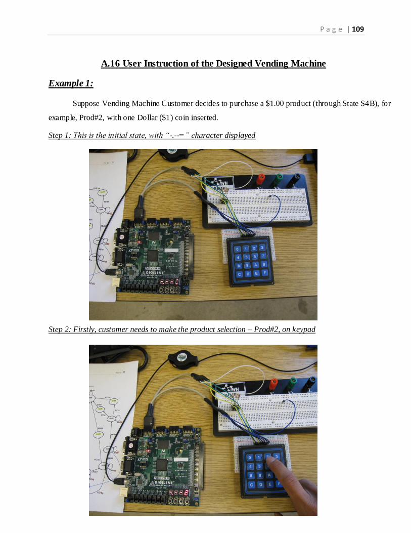
P a g e | 109
A.16 User Instruction of the Designed Vending Machine
Example 1:
Suppose Vending Machine Customer decides to purchase a $1.00 product (through State S4B), for
example, Prod#2, with one Dollar ($1) coin inserted.
Step 1: This is the initial state, with “-.--=” character displayed
Step 2: Firstly, customer needs to make the product selection – Prod#2, on keypad
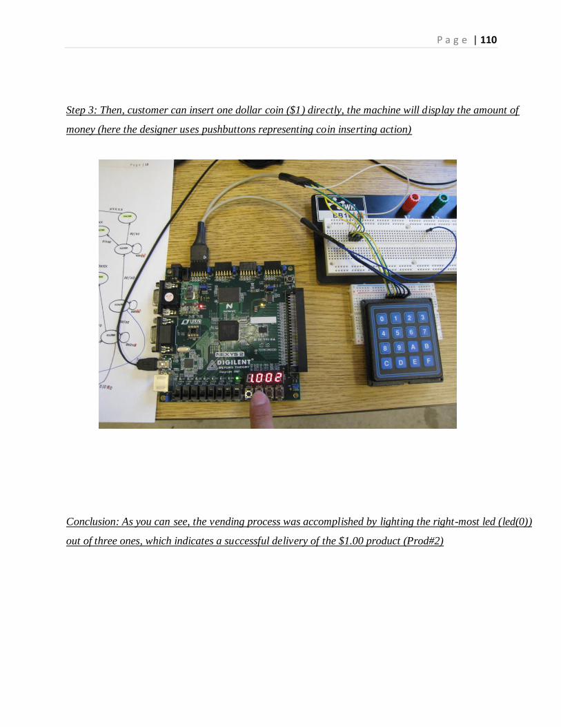
P a g e | 110
Step 3: Then, customer can insert one dollar coin ($1) directly, the machine will display the amount of
money (here the designer uses pushbuttons representing coin inserting action)
Conclusion: As you can see, the vending process was accomplished by lighting the right-most led (led(0))
out of three ones, which indicates a successful delivery of the $1.00 product (Prod#2)
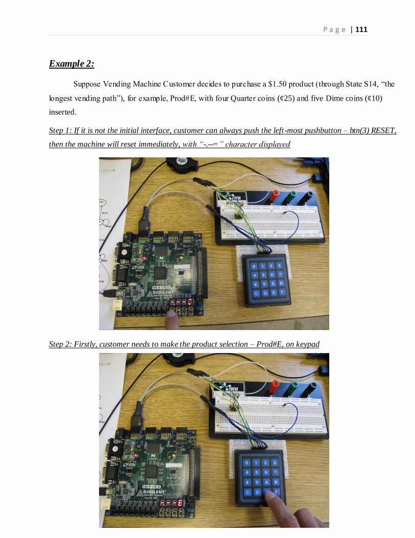
P a g e | 111
Example 2:
Suppose Vending Machine Customer decides to purchase a $1.50 product (through State S14, “the
longest vending path”), for example, Prod#E, with four Quarter coins (¢25) and five Dime coins (¢10)
inserted.
Step 1: If it is not the initial interface, customer can always push the left-most pushbutton – btn(3) RESET,
then the machine will reset immediately, with “-.--=” character displayed
Step 2: Firstly, customer needs to make the product selection – Prod#E, on keypad
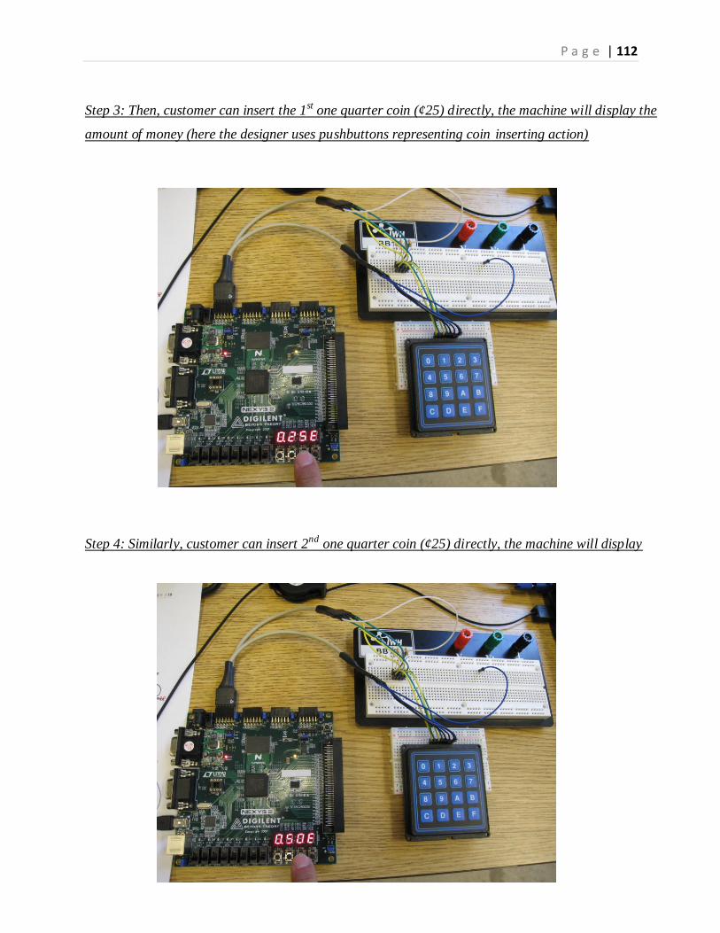
P a g e | 112
Step 3: Then, customer can insert the 1st one quarter coin (¢25) directly, the machine will display the
amount of money (here the designer uses pushbuttons representing coin inserting action)
Step 4: Similarly, customer can insert 2nd one quarter coin (¢25) directly, the machine will display
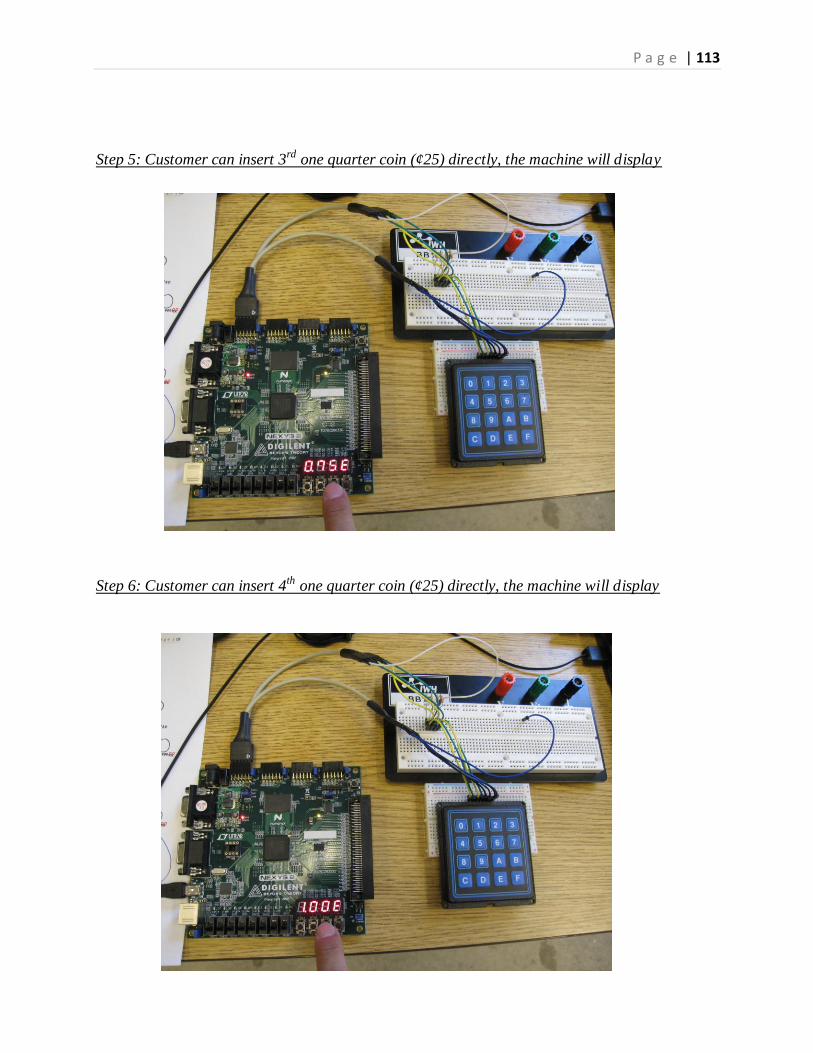
P a g e | 113
Step 5: Customer can insert 3rd one quarter coin (¢25) directly, the machine will display
Step 6: Customer can insert 4th one quarter coin (¢25) directly, the machine will display
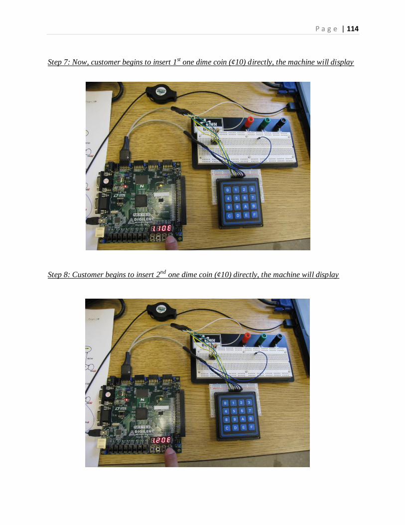
P a g e | 114
Step 7: Now, customer begins to insert 1st one dime coin (¢10) directly, the machine will display
Step 8: Customer begins to insert 2nd one dime coin (¢10) directly, the machine will display
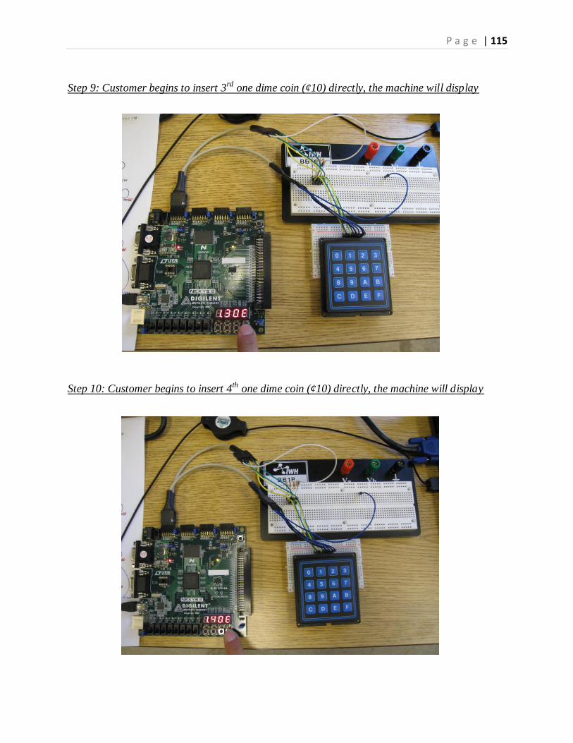
P a g e | 115
Step 9: Customer begins to insert 3rd one dime coin (¢10) directly, the machine will display
Step 10: Customer begins to insert 4th one dime coin (¢10) directly, the machine will display
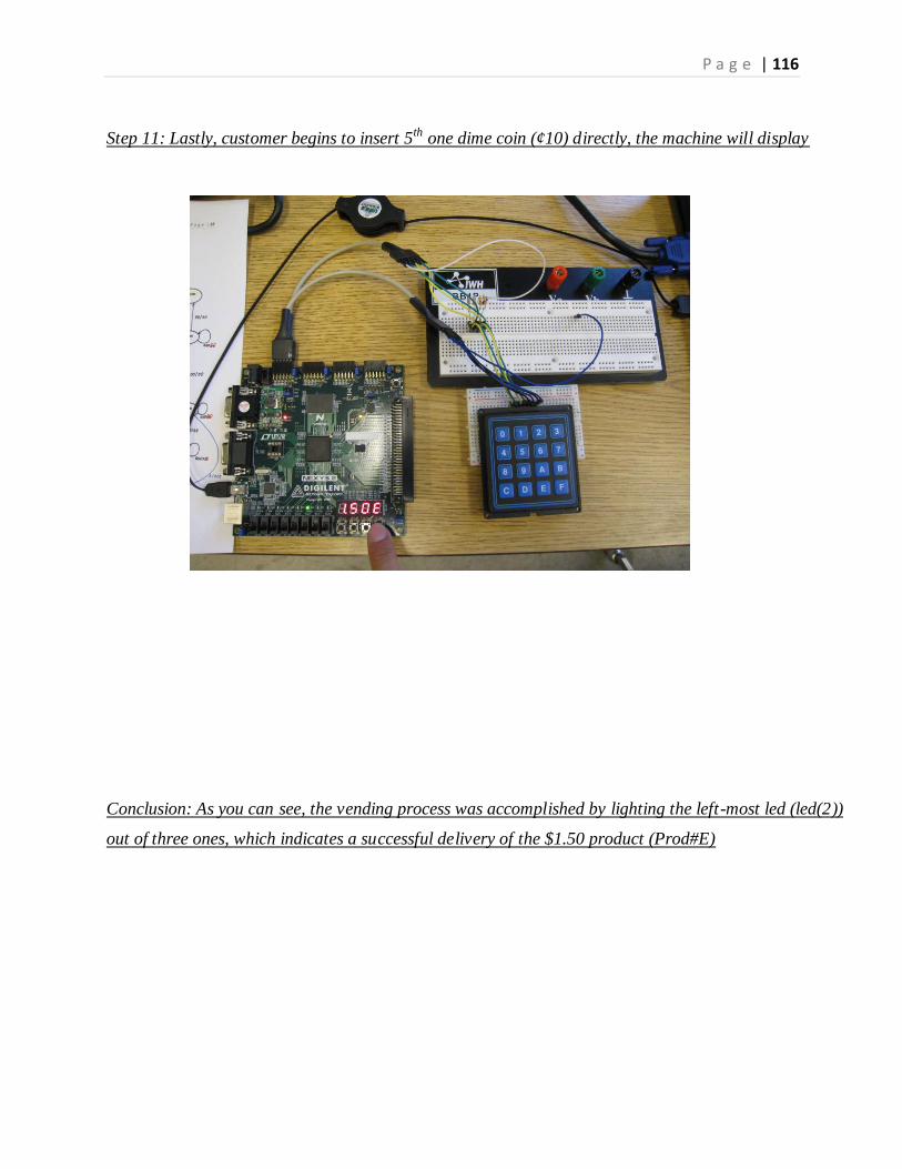
P a g e | 116
Step 11: Lastly, customer begins to insert 5th one dime coin (¢10) directly, the machine will display
Conclusion: As you can see, the vending process was accomplished by lighting the left-most led (led(2))
out of three ones, which indicates a successful delivery of the $1.50 product (Prod#E)
Recommended


![[NCKU] Simulation and Verification with Altera FPGA](https://img.pdfslide.net/doc/110x75/55295cbf550346522e8b4745/ncku-simulation-and-verification-with-altera-fpga.jpg)