The Fujitsu 56GSa/s Analog-to-Digital Converter Enables 100GbE Transport
Ultra-fast CMOS ADC Provides Technology Breakthrough for Upcoming Telecommunication Applications
T e c h n o l o g y B a c k g r o u n d e r
The Fujitsu 56GSa/s Analog-to-Digital Converter Enables 100GbE Transport
Introduction to Analog-to-Digital Converter for 100Gbps Systems
A 100Gbps coherent receiver needs four 56GSa/s Analog-to-Digital Converters (ADCs) and a tera-OPS DSP that dissipates only tens of watts. This paper discusses the forces pushing towards a single-chip CMOS solution. The paper also introduces the Fujitsu ultra-fast CMOS ADC, which provides the enabling technology for 100Gbps Ethernet and OTU-4 transport systems using coherent receivers.
To provide a long-haul 100Gbps optical transport network with maximum reach and immunity to optical fiber non-idealities, the industry has settled on dual-polarization, quadrature, phase-shift keying (DP-QPSK) as a modulation method. This means that a coherent receiver is required. The biggest implementation challenge resulting from this decision is the need for low-power, ultra-high-speed ADCs. Their technology requirements define the way such a receiver can be implemented.
Without suitable ADCs – especially without those with low enough power consumption – it is impossible to produce a 100Gbps coherent receiver that is useful for a commercial optical network (as opposed to a prototype system suitable only for demonstration in the lab). Also, in the future such ADCs will be required for higher-speed short-haul links, where low power and cost become even more important because there are many more short-haul links than long-haul ones.
These ADCs need sampling rates of at least 56GSa/s and resolution of 6 bits or more. Power consumption
needs to be no more than a few watts each to fit within the power constraints imposed by the system. Until recently it was thought that technology such as very advanced SiGe or ultra-small-geometry CMOS (40nm or smaller) would be needed to meet these requirements and still have the sufficient dynamic range for input signals up to 15GHz and higher. By extrapolating from historic advances in ADC design it was predicted at the end of 2008 that suitable ADCs would not be available until 20131.
However, the development of new circuit techniques means that these ADCs actually became available in 2009 using 65nm CMOS2. This accelerated the date by when single-chip 100Gbps coherent receivers became technically and economically feasible, and significantly changed the industry roadmap for these devices.
In addition to covering the technical issues described above, this paper discusses Fujitsu’s first customer evaluation silicon (ROBIN) for the CHArge-mode Interleaved Sampling (CHAIS) technology containing a two-channel 56GSa/s version of the ADC.
The Drive Towards a Single-Chip CMOS ADC DSP
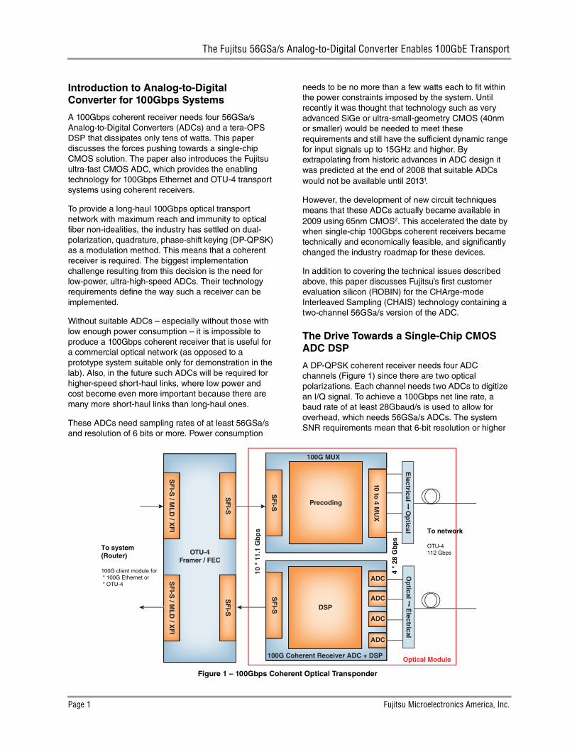
A DP-QPSK coherent receiver needs four ADC channels (Figure 1) since there are two optical polarizations. Each channel needs two ADCs to digitize an I/Q signal. To achieve a 100Gbps net line rate, a baud rate of at least 28Gbaud/s is used to allow for overhead, which needs 56GSa/s ADCs. The system SNR requirements mean that 6-bit resolution or higher
SF
I-SS
FI-S
SF
I-S / M
LD
/ XF
IS
FI-S
/ ML
D / X
FI
OTU-4Framer / FEC
10 *
11.
1 G
bp
s
SF
I-SS
FI-S Precoding
DSP
10 to 4 M
UX
ADC
ADC
ADC
ADC
Electrical O
ptical
Op
tical Electrical
Optical Module
To system(Router)
100G client module for * 100G Ethernet or * OTU-4
To network
OTU-4112 Gbps
4 *
28 G
bp
s
100G Coherent Receiver ADC + DSP
100G MUX
Figure 1 – 100Gbps Coherent Optical Transponder
Page 1 Fujitsu Microelectronics America, Inc.
The Fujitsu 56GSa/s Analog-to-Digital Converter Enables 100GbE Transport
is typically required to allow some margin for added noise and distortion. So, for four ADCs, the output data rate to the DSP is 1.3Tb/s – or 1.8Tb/s if 8-bit resolution is used to allow more margin and/or digital AGC after the ADC.
If the ADCs are not integrated with the DSP, this huge amount of data has to be transmitted between the chips, which is not only difficult to implement (a very large number of channels with a high data rate), but uses a lot of power for serialization, de-serialization and transmission. Even using an optimistic figure of 100mW/ch for an 11Gbps channel (ADC transmit + DSP receive), this means 3-4W per ADC is needed just to transfer the data. This is acceptable for a prototype or demonstrator, but not for a production solution.
A 100Gbps receiver DSP – which performs functions such as equalization, chromatic dispersion compensation, and data recovery – needs on the order of 50M gates. This mandates the use of CMOS. The system power requirement for a complete coherent receiver is only a few tens of watts. Since a 40G ADCDSP chip in 90nm already dissipates more than 20W3, geometries of 65nm or smaller, as well as power-efficient design techniques, are needed for a 100G receiver.
This implies that the ADC should also use CMOS, though this makes the design extremely challenging. A single-chip solution is really the only viable way forward, especially to take advantage of future CMOS technology improvements. However, this assumes that the ADC performance scales similarly to digital circuits, which may not be true for conventional ADCs. Even if a multi-chip solution could be built (e.g., using SiGe ADCs together with a CMOS DSP in a multi-chip module), the overall power would be higher, the production cost greater and the yield of such a complex solution inevitably lower. This approach also does not provide a good roadmap towards even lower-power and cost-effective solutions for short-haul and beyond 100Gbps.
56GSa/s CMOS ADC Challenges
Designing a 56GSa/s 6-8b ADC in any technology presents major difficulties. These are made worse here because available power for the ADC+DSP is limited both by the supply capability and thermal dissipation. A reasonable target is 10W or less for a complete 4-channel ADC, which means little more than 2W per ADC cell. Conventional ADCs with this level of performance dissipate much more power than this, due to the high power needed for the wideband sampling/
demultiplexing front-end and clock circuits, as well as the back-end ADC power.
To achieve such high speed and resolution, multiple lower-rate interleaved ADCs are used, driven by one or more wideband sample-and-hold (S/H) circuits, usually with more demultiplexing in between. The S/H circuits need very wide bandwidth and low distortion, which is why either SiGe or very small geometry CMOS (40nm or smaller) is normally said to be needed for 56GSa/s. However, with the sub-1V supply voltages imposed by 40nm CMOS, it is difficult to design an S/H with reasonably large signal swing (to preserve SNR) and linearity (to preserve THD). Higher-voltage SiGe avoids these problems, but dissipates much more power.
The small device sizes available in modern CMOS processes combine low power consumption and high density with high speed, but this comes at the price of increased noise and mismatch. The normal solution to this is to increase transistor sizes (gate length and/or width), but this is not possible here because it is not feasible to reduce bandwidth or increase power consumption. Small transistors mean poor matching in both S/H and ADC, not just in the signal paths but also in the clock paths, where 100fs clock skew causes -40dBc distortion for a 16GHz input signal. The only feasible way to reduce these mismatch-induced errors is by widespread on-chip calibration.
Providing clock-skew adjustment is not so difficult in theory. Measuring and calibrating skew down to sub-pico-second accuracy is a much bigger problem, especially maintaining this accuracy over time and environmental variations without taking the ADC off-line for calibration or needing a large amount of complex data analysis to calculate the errors.
CHArge-mode Interleaved Sampling (CHAIS) ADC
One way to overcome these challenges is to use a new sampler/demultiplexer architecture2 which gives the linearity, noise and bandwidth required without needing extremely short-channel (40nm or below) transistors. The new architecture also allows simple calibration of amplitude and timing errors during operation and dissipates <0.5W. Instead of a conventional S/H using analog switches and sampling capacitors, the CHAIS circuit generates controlled-shape constant-area (CHArge) sampling pulses, which are then demultiplexed to drive a large array of 8b SAR ADCs (320x175Ms/s).
Using SAR ADCs instead of full-flash means that increasing resolution from 6b to 8b has only a small
Page 2 Fujitsu Microelectronics America, Inc.

The Fujitsu 56GSa/s Analog-to-Digital Converter Enables 100GbE Transport
penalty in power and area, but the increased resolution reduces quantization noise and allows more margin for other noise contributions. The SAR ADCs also open up the possibility of doing some AGC digitally after the ADC instead of in the optical front-end. This approach has the advantage of perfect channel matching even with rapid gain changes to track optical power variations. SAR ADCs also scale well with smaller technology since most of the power is digital.
The high circuit density of CMOS is used to good effect by having a large number of calibration DACs (more then 400 per ADC) to trim out all significant device mismatches in the signal path, including timing (skew) as well as amplitude (gain and offset) errors. The way that the CHAIS circuit (Figure 2) works means that all these errors can be calculated in real-time in the background by simple analysis of all the ADC digital output data. This analysis is done inside the ADC. The results are then read out at a much lower rate (microseconds to tens of milliseconds) and used to drive a low-complexity convergence algorithm with a time constant of typically less than a second. That algorithm provides convergence at power-up and continuously during operation to track any parameter drift.
DSP and Integration Issues
Realizing the DSP for a 100Gbps coherent receiver is hardly trivial, not just because of the high processing power required (12 TOPS were needed3 for a 40Gbps receiver), but because the wide data paths (thousands of bits wide) are needed to keep clock rates reasonably low to improve power efficiency. (High clock rates need more latches to reduce logic depth, which increases power consumption.)
The design problem then becomes one of interconnect, not gate count. Unfortunately, design tools and designers tend to design the circuits first and just accept the resulting interconnect. This should be the other way around or the resulting DSP design can be difficult or even impossible to lay out.
Even assuming that the ADC and DSP can be designed separately, other major problems need to be overcome when integrating the two in a single chip 100Gbps coherent receiver. Noise coupling between digital and analog is one obvious issue. By looking at approximate numbers the sheer scale of the problem becomes apparent.
Clocks
Trim Voltages
Input
DE
MU
XA
DE
MU
XB
DE
MU
XC
DE
MU
XD
ADCBANKA
ADCBANKB
ADCBANKC
ADCBANKD
Dig
ital
880 x 8b ADC Outputs80 x ADC Inputs
Output1024b437.5MHz
4 Phase Sampler
14GHz VCO(1 per ADC pair)
Calibration
80
80
80
80
80
80
80
80
DEMUX
Figure 2 – Single 56GSa/s ADC Solution: CHArge-mode Interleaved Sampler
Page 3 Fujitsu Microelectronics America, Inc.

The Fujitsu 56GSa/s Analog-to-Digital Converter Enables 100GbE Transport
For example, a large DSP with peak switching currents of ~100A (and perhaps ~100mV supply noise) could be on the same die as ADCs which need to have jitter of the order of 100fs. Assuming a reasonable supply noise delay sensitivity of 1ps/mV for the clock path, the analog supply noise needs to be ~0.1mV, which means ~60dB isolation between analog and digital regions.
This might not seem so difficult except that the bandwidth of this noise coupling is many GHz because – unlike “normal” analog or RF circuits – there’s nothing to band-limit the noise. At these frequencies noise-isolation methods such as triple-well are no longer effective. In fact, given the frequencies and bandwidths involved and the jitter requirements, the noise-coupling problem is probably more difficult than on any previously realized mixed-signal chip. However, it can be solved by careful design, some new noise isolation techniques, and perhaps a touch of “black magic”4.
It is obviously undesirable to allow large DSP current spikes to get out of the package and into the PCB, both for good EMC performance and to prevent them from interfering with the analog circuits. Relying on PCB decoupling also gives the end user a perfect opportunity to get this wrong and degrade the performance in an unpredictable manner.
Ultra-low-inductance decoupling inside the customized flip-chip package and on the chip solves this problem, but any resonances between the internal “L” and “C” are then very high “Q” and always fall in the hundreds of MHz region. So just adding decoupling on the “more is better” principle can do more harm than good. Simulations of the entire chip and package together are
needed. It will usually be necessary to take steps to damp the power-supply resonances such as damped on-chip decoupling and/or controlled-ESR ceramic decouplers in the package.
The Fujitsu Solution
The Fujitsu CMOS ADC provides the enabling technology for upcoming telecommunication applications such as 100Gbps Ethernet and OTU-4 transport systems using coherent receivers. The ADC uses Fujitsu’s revolutionary CHArge-mode Interleaved Sampler technology (CHAIS), which allows the implementation of extremely fast, high-resolution ADCs in CMOS process technology (Figure 3 and 4).
Major benefits of the CHAIS ADC are low power consumption and the option to be integrated with millions of gates onto the same die using Fujitsu’s standard 65nm CMOS process technology. In combination with Fujitsu’s leading flip-chip packaging technology, the ultra-fast ADC is ideal for applications that require high-performance analog and digital processing power.
With an effective resolution bandwidth of >15GHz and a sample rate of 56GSa/s, the ADC is at the leading edge of converter performance. The macro employs a self-contained background-calibration technique for sampler
SAR ADCarray
SAR ADCarray
PLL SamplerSampler
Demux Demux
AD
C R
efs
ADC logic
Waveform memory
Bias
SAR ADCarray
SAR ADCarray
PLL SamplerSampler
Demux Demux
AD
C R
efs
ADC logic
Waveform memory
Bias
Figure 3 – 56GSa/s ADC Two-Channel Version Using CHAIS
AHIP
AHIN
HREF (4:1)
AHQP
AHQNRREF
REFCLKP
REFCLKNBGAPAVIP
AVIN
VREF (4:1)
AVQP
AVQN
VSPI_OUT
VQD (1023:0)
VID (1023:0)
XSSRDYCLKO
SPI_IN
CAL_OVRRNG
M40G
CLKDIV
EN
XRST
HSPI_OUTHID (1023:0)
HQD (1023:0)
VSSVD
D
AVSADC
AVDAD
C
AVD33
AVDN
EG
AVSAVD
RF
AVDBB
I ADC
Q ADC
I ADC
Q ADC
‚N
PLL
ADC D
igital
REFS
PLL
ADC D
igital
REFS
Figure 4 – 56GSa/s ADC Four-Channel Version
Page 4 Fujitsu Microelectronics America, Inc.
interleave-timing skew, as well as linearity and offset. The calibration block also contains an alarm function, which can be used as an interrupt to warn the system when the internal calibration reaches a pre-defined or programmable percentage of its calibration range.
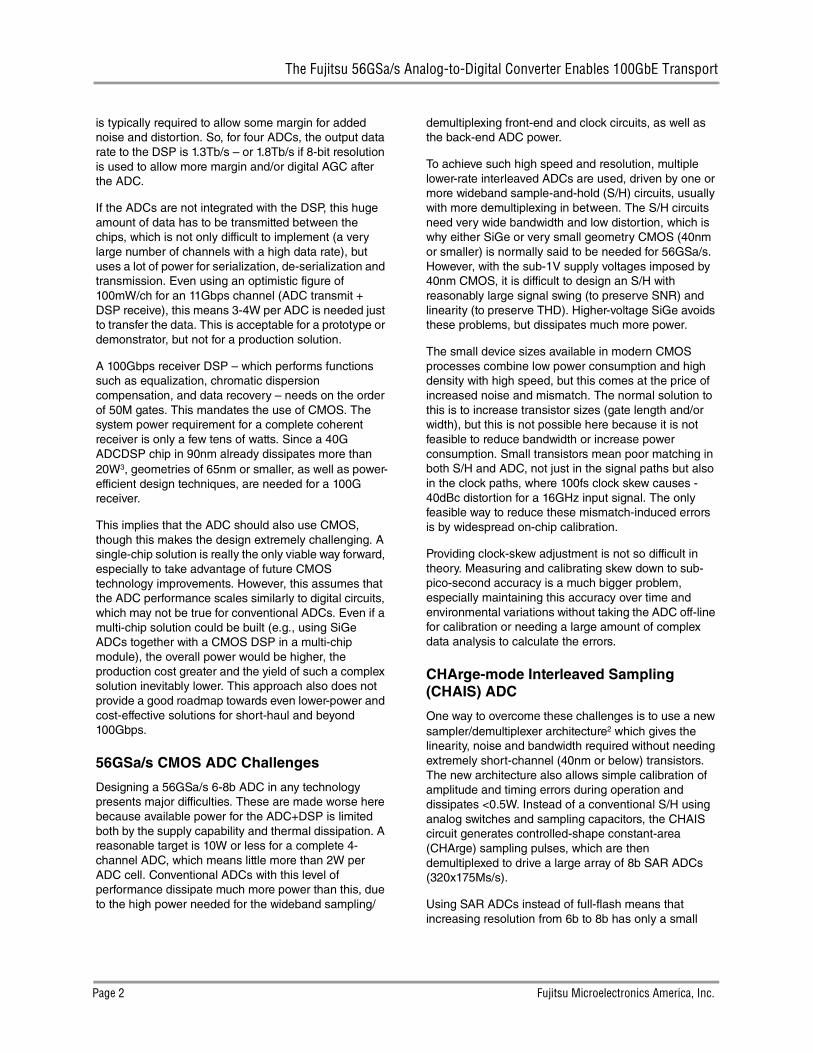
The first customer evaluation silicon (ROBIN) for the CHAIS technology contains a two-channel 56GSa/s version of the ADC (Figure 3). The on-chip RAM of ROBIN stores 16k x 8-bit samples for each ADC. The data can be accessed by reading this memory as there is no external output from the converter. Several storage modes that enable control of the RAMS from external triggers are available.
Other versions of the ADC with lower and higher sampling rates, and different channel configurations, are in development or planned.
Development Kits
A development kit (Figure 5) for the two-channel 56GSa/s ADC evaluation test chip is available in a ceramic package (ROBIN).
Each kit includes everything needed to minimize the time to getting started, including:
• BATBOARD evaluation board with the choice of ROBIN being solder mounted or mounted with a socket
• Calibration board with the device mounted on it
• High-frequency splitter board
• Interconnect boards
• PC programming interface board
• Software
The 56GSa/s ADC evaluation board (BATBOARD) is intended to allow rapid characterization of the ADC. Two variations of the board are available. The first board is mounted with a low inductance socket, which allows rapid replacement of the device under test. The socket incorporates a heat sink for increased heat dissipation. The heat sink can also be used with temperature-forcing systems to precisely control the die temperature. The second board has the device mounted directly onto it. Special attention has been given to the connector choice to allow connection to
instrumentation, which will perform the design-verification tests. The printed circuit board utilizes high-performance materials to optimize the integrity of the signals. The development kit also includes Fujitsu’s serial interface cable (ref DKSERIAL-1), which allows the device to be programmed through a Windows® application running on a host PC.
Conclusion
New ADC techniques make it feasible, for the first time, to design single-chip 100Gbps coherent receivers in 65nm CMOS that meet the performance and power requirements of long-haul optical systems. These receivers provide a way forward for future short-haul and higher-rate applications with migration to 40nm and beyond. Being able to design a suitable ADC only solves part of the problem of producing such an ADCDSP. The mixed-signal integration issues are at least as challenging, but can be solved by sufficiently “intelligent design.”
For More Information
For more information on the Fujitsu Analog-to-Digital Converter, please go tohttp://us.fujitsu.com/micro/sms/56gadc or address e-mail to [email protected]
Red — Top layer differential pair
Black — Bottom layer differential pair
Gold — Gold layer coplanar wave guide (ADC inputs)Pow
er connectorsand bulk decoupling
CLK CLK
CLK
ADC
TX
DAT DAT
XFP
Programm
inginterface
SMA connectors4cm pich for direct
connection to DCA-J
2.4mm connectors
Figure 5 – A 56GSa/s 8-bit ADC Development Kit
8
©2010 Fujitsu Microelectronics America, Inc. All rights reserved.All company and product names are trademarks or registered trademarks of their respective owners. Printed in U.S.A. SMS-TB-21368-05/2010
FUJITSU MICROELECTRONICS AMERICA, INC.Corporate Headquarters1250 East Arques Avenue, M/S 333, Sunnyvale, California 94085-5401Tel: (800) 866-8608 Fax: (408) 737-5999E-mail: [email protected] Web Site: http://us.fujitsu.com/micro
ReferencesPaper presented at the Optical Society of America in 2010 by Ian Dedic, Fujitsu Microelectronics Europe GmbH, Maidenhead, Berkshire, United Kingdom.1 http://www.lightreading.com/document.asp?doc_id=161755&page_number=9 2 http://www.chais.info 3 http://conference.vde.com/ecoc-2009/programs/documents/ws1_12_johnsitch.pdf 4 Howard W. Johnson, High-Speed Signal Propagation -- Advanced Black Magic (Prentice Hall, 2003)
Recommended