Trusted Fabrication through 3D Integration
Paul Franzon, Steve LipaDepartment of Electrical and Computer Engineering,
NC State [email protected] , [email protected]
Lisa McIlrath, Draper
1
Outline
• 3D Technology Review• 3D Projects at NCSU• Trusted Fabrication Project
– Opportunity and Threats– Obfuscation– Technology– Simulation Demonstration– Future Work
2
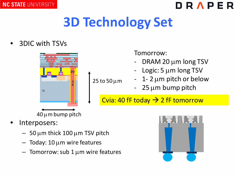
3D Technology Set• 3DIC with TSVs
• Interposers:– 50 µm thick 100 µm TSV pitch– Today: 10 µm wire features– Tomorrow: sub 1 µm wire features
40 µm bump pitch
25 to 50 µm
Tomorrow:- DRAM 20 µm long TSV- Logic: 5 µm long TSV- 1- 2 µm pitch or below- 25 µm bump pitch
Cvia: 40 fF today 2 fF tomorrow
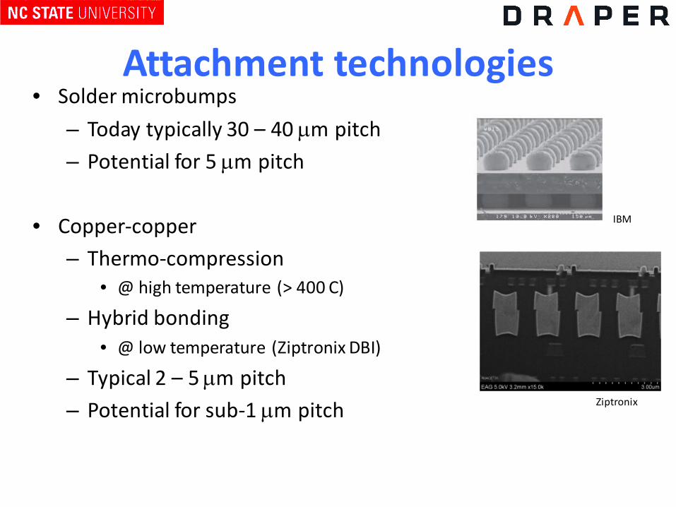
Attachment technologies• Solder microbumps
– Today typically 30 – 40 µm pitch – Potential for 5 µm pitch
• Copper-copper – Thermo-compression
• @ high temperature (> 400 C)
– Hybrid bonding• @ low temperature (Ziptronix DBI)
– Typical 2 – 5 µm pitch– Potential for sub-1 µm pitch
IBM
Ziptronix
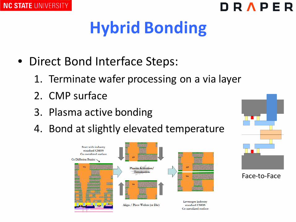
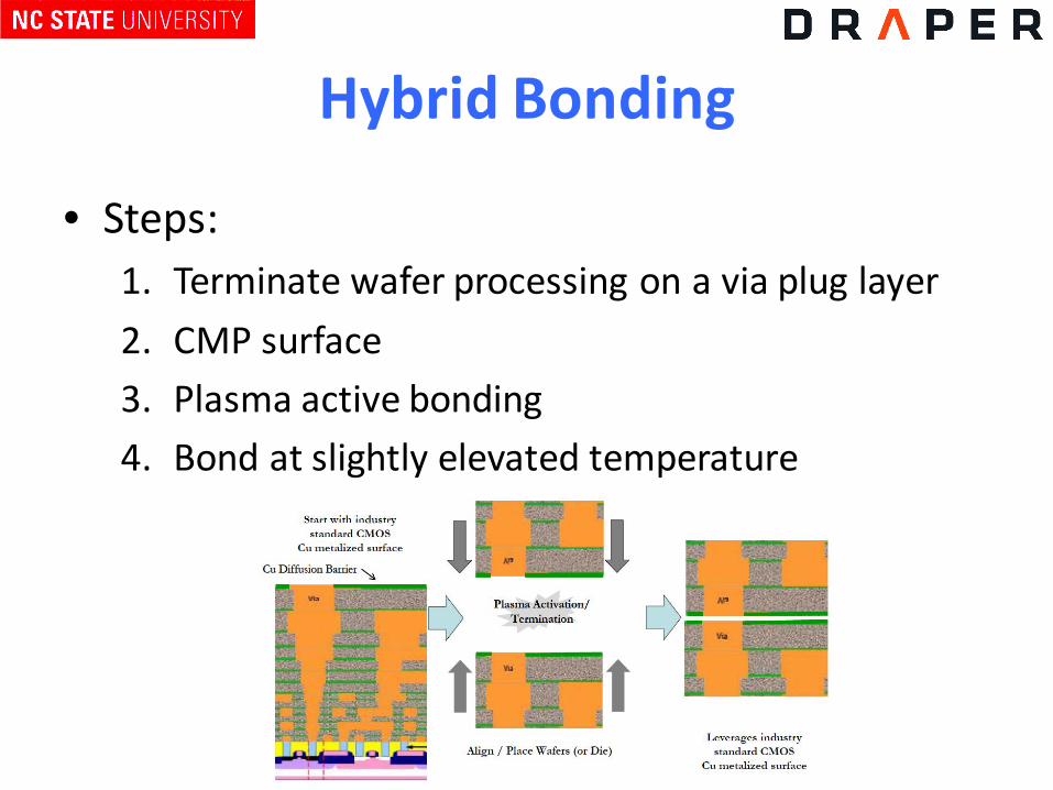
Hybrid Bonding
• Direct Bond Interface Steps:1. Terminate wafer processing on a via layer2. CMP surface3. Plasma active bonding4. Bond at slightly elevated temperature
Face-to-Face
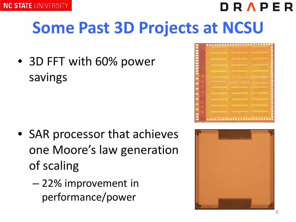
Some Past 3D Projects at NCSU
• 3D FFT with 60% power savings
• SAR processor that achieves one Moore’s law generation of scaling– 22% improvement in
performance/power6
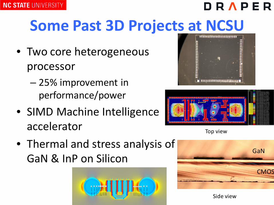
Some Past 3D Projects at NCSU• Two core heterogeneous
processor– 25% improvement in
performance/power
• SIMD Machine Intelligence accelerator
• Thermal and stress analysis of GaN & InP on Silicon
Top view
Side view
GaN
CMOS
Just starting / Future Projects
• Demonstration of obfuscation through 3D integration – Continuation of this project
• 2.5D integration of chiplets for machine learning and machine intelligence (DARPA chips program)
• Reliability evaluation– With Vanderbilt (future)
8
Outline
• 3D Technology Review• 3D Projects at NCSU• Trusted Fabrication Project
– Opportunity and Threats– Obfuscation– Technology– Simulation Demonstration– Future Work
9
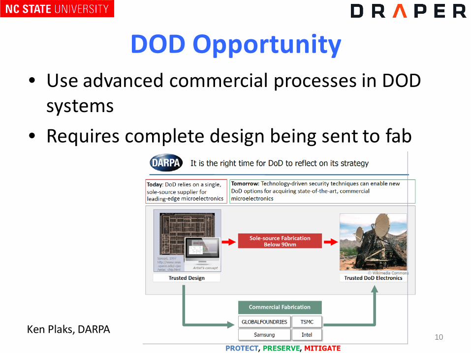
DOD Opportunity• Use advanced commercial processes in DOD
systems• Requires complete design being sent to fab
10Ken Plaks, DARPA
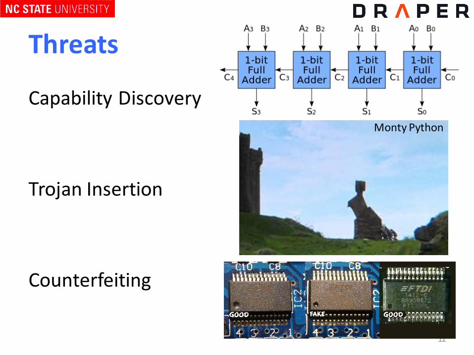
Threats
Capability Discovery
Trojan Insertion
Counterfeiting
11
Monty Python
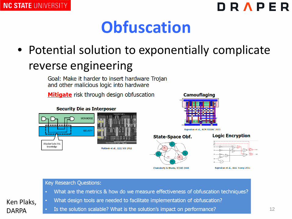
Obfuscation• Potential solution to exponentially complicate
reverse engineering
12Ken Plaks, DARPA
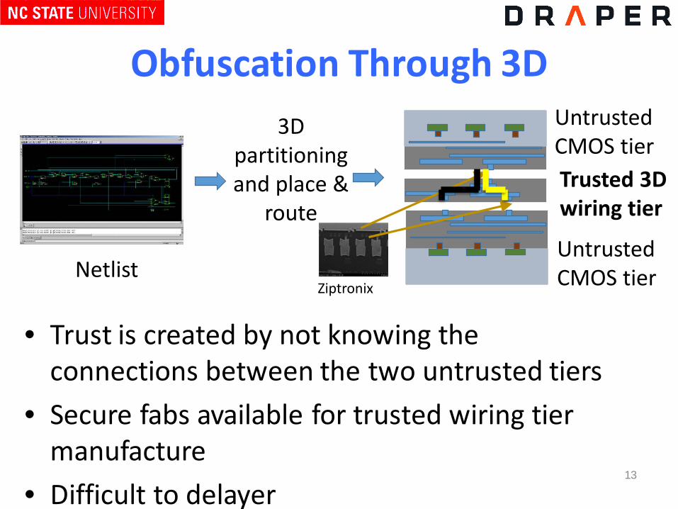
Obfuscation Through 3D
• Trust is created by not knowing the connections between the two untrusted tiers
• Secure fabs available for trusted wiring tier manufacture
• Difficult to delayer 13
Netlist
3D partitioning and place &
route
Untrusted CMOS tier
Untrusted CMOS tier
Trusted 3D wiring tier
Ziptronix
Hybrid Bonding
• Steps:1. Terminate wafer processing on a via plug layer2. CMP surface3. Plasma active bonding4. Bond at slightly elevated temperature
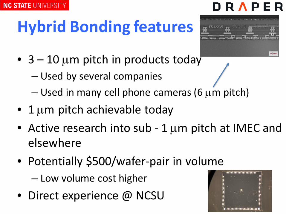
Hybrid Bonding features
• 3 – 10 µm pitch in products today– Used by several companies– Used in many cell phone cameras (6 µm pitch)
• 1 µm pitch achievable today• Active research into sub - 1 µm pitch at IMEC and
elsewhere • Potentially $500/wafer-pair in volume
– Low volume cost higher
• Direct experience @ NCSU15
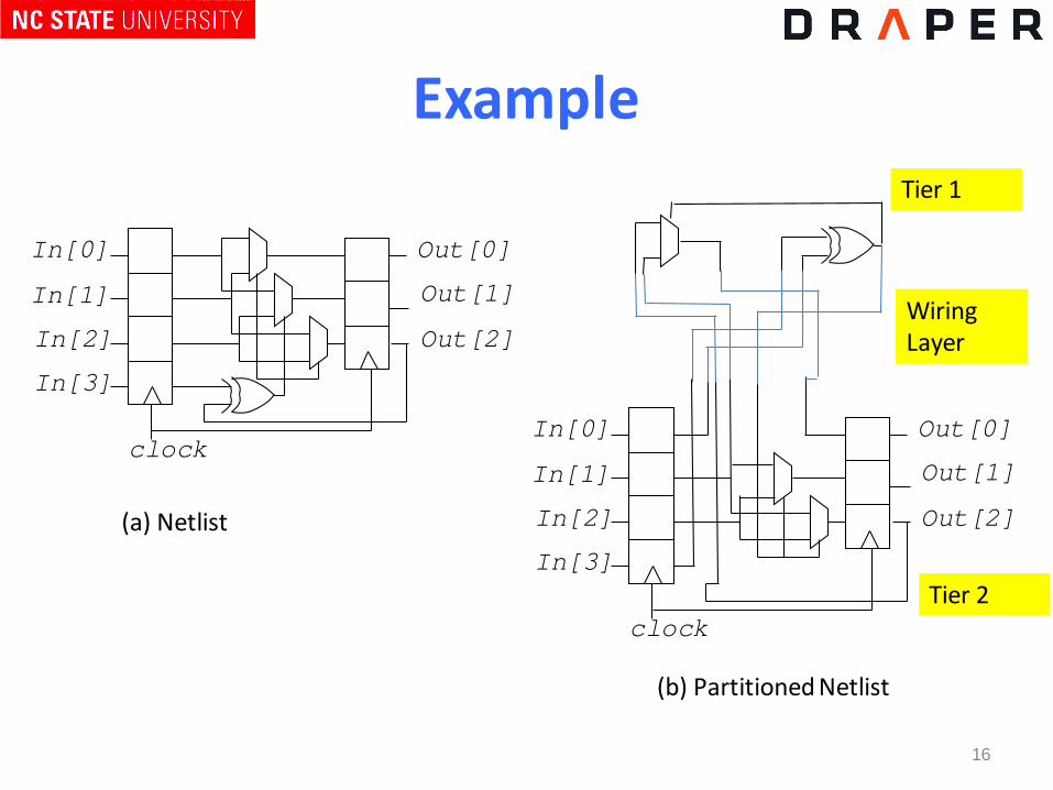
Example
16
In[0]
In[1]
In[2]
In[3]
clock
Out[0]
Out[1]
Out[2]
(a) Netlist
In[0]
In[1]
In[2]
In[3]
clock
Out[0]
Out[1]
Out[2]
(b) Partitioned Netlist
Tier 1
Tier 2
Wiring Layer
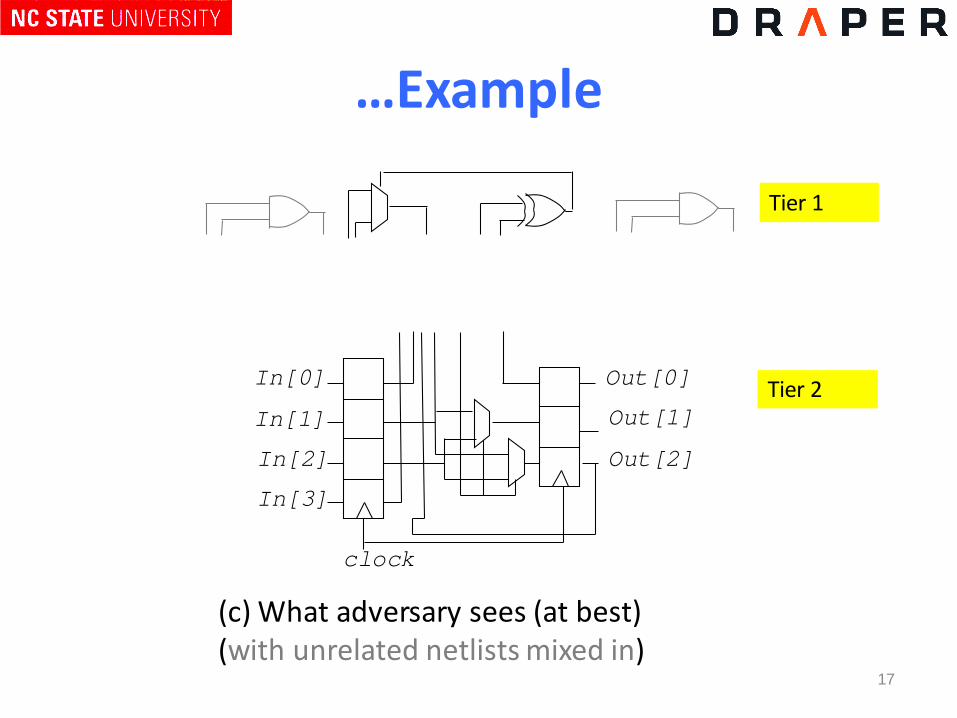
…Example
17
In[0]
In[1]
In[2]
In[3]
clock
Out[0]
Out[1]
Out[2]
(c) What adversary sees (at best)(with unrelated netlists mixed in)
Tier 1
Tier 2
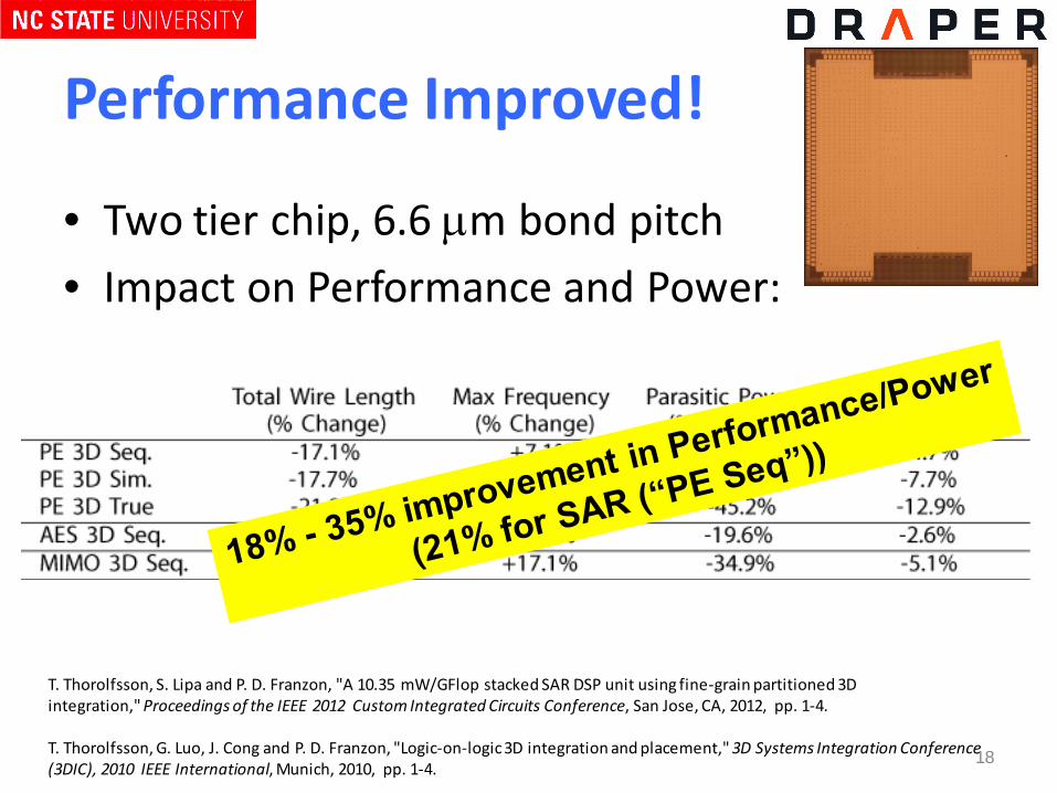
Performance Improved!
• Two tier chip, 6.6 µm bond pitch• Impact on Performance and Power:
18
T. Thorolfsson, S. Lipa and P. D. Franzon, "A 10.35 mW/GFlop stacked SAR DSP unit using fine-grain partitioned 3D integration," Proceedings of the IEEE 2012 Custom Integrated Circuits Conference, San Jose, CA, 2012, pp. 1-4.
T. Thorolfsson, G. Luo, J. Cong and P. D. Franzon, "Logic-on-logic 3D integration and placement," 3D Systems Integration Conference (3DIC), 2010 IEEE International, Munich, 2010, pp. 1-4.
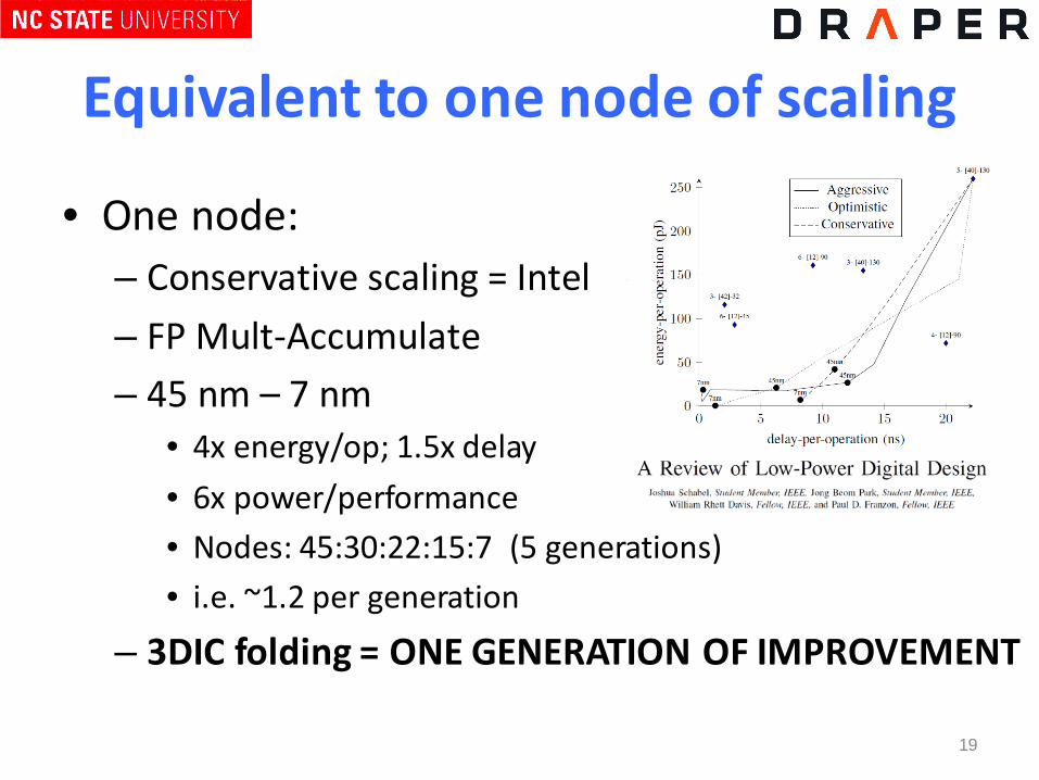
Equivalent to one node of scaling
• One node:– Conservative scaling = Intel– FP Mult-Accumulate– 45 nm – 7 nm
• 4x energy/op; 1.5x delay• 6x power/performance• Nodes: 45:30:22:15:7 (5 generations)• i.e. ~1.2 per generation
– 3DIC folding = ONE GENERATION OF IMPROVEMENT
19
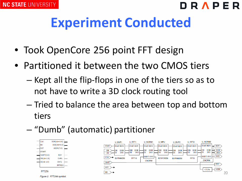
Experiment Conducted
• Took OpenCore 256 point FFT design• Partitioned it between the two CMOS tiers
– Kept all the flip-flops in one of the tiers so as to not have to write a 3D clock routing tool
– Tried to balance the area between top and bottom tiers
– “Dumb” (automatic) partitioner
20
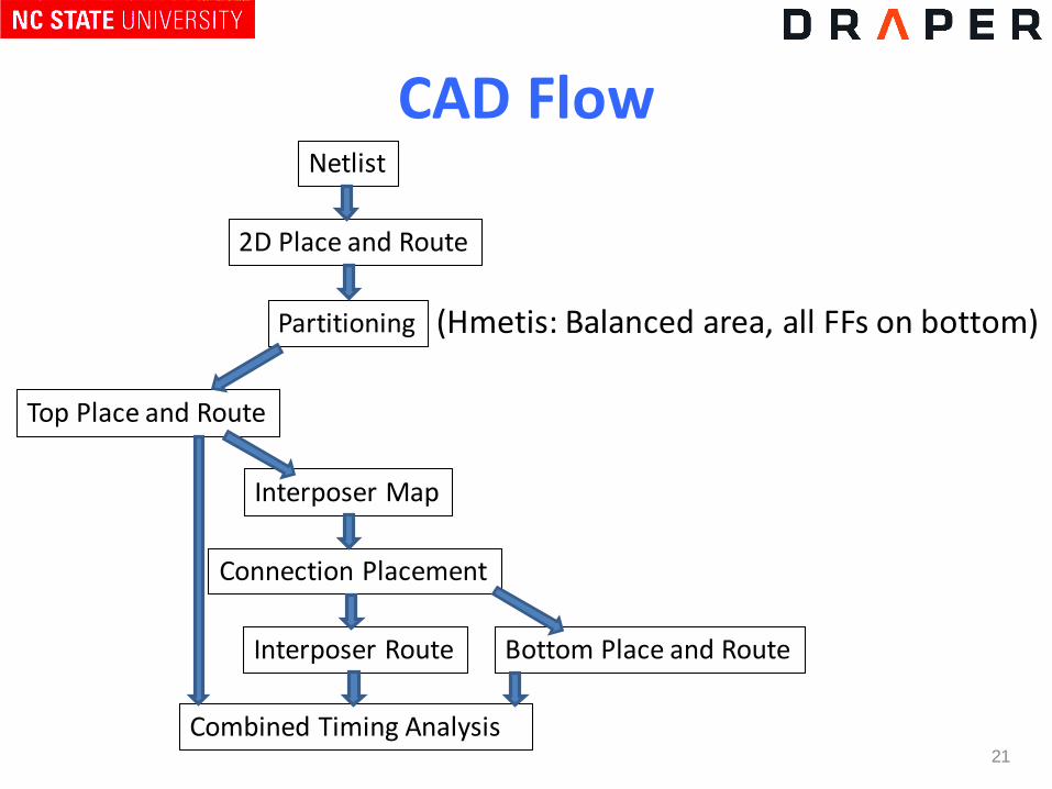
CAD Flow
21
Netlist
2D Place and Route
Partitioning
Top Place and Route
Interposer Map
Connection Placement
Bottom Place and RouteInterposer Route
Combined Timing Analysis
(Hmetis: Balanced area, all FFs on bottom)
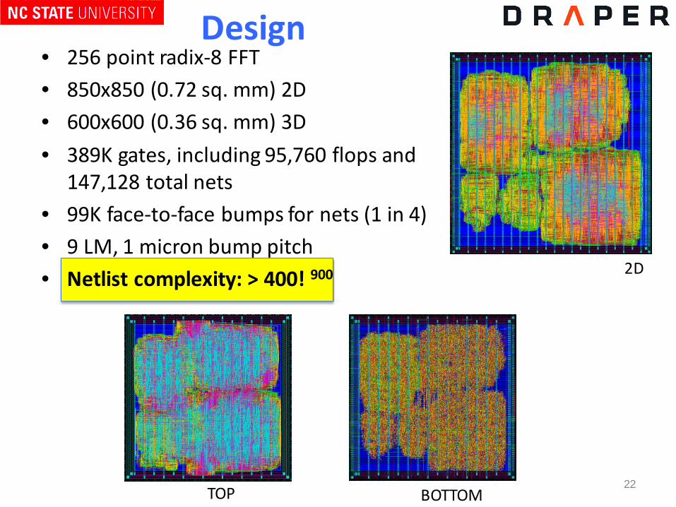
Design• 256 point radix-8 FFT• 850x850 (0.72 sq. mm) 2D• 600x600 (0.36 sq. mm) 3D• 389K gates, including 95,760 flops and
147,128 total nets • 99K face-to-face bumps for nets (1 in 4)• 9 LM, 1 micron bump pitch• Netlist complexity: > 400! 900
22
2D
TOP BOTTOM
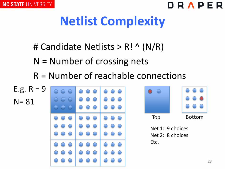
Netlist Complexity
# Candidate Netlists > R! ^ (N/R)N = Number of crossing netsR = Number of reachable connections
E.g. R = 9N= 81
23
Top Bottom
Net 1: 9 choicesNet 2: 8 choicesEtc.
Red Teaming
• 6.5 man weeks of effort• Not able to reverse engineer netlist• Was able to obtain functionality of certain
combinational logic blocks– Could indicate partial capability and could be
basis for Trojan insertion– Made easier by “dumb partitioning”
24
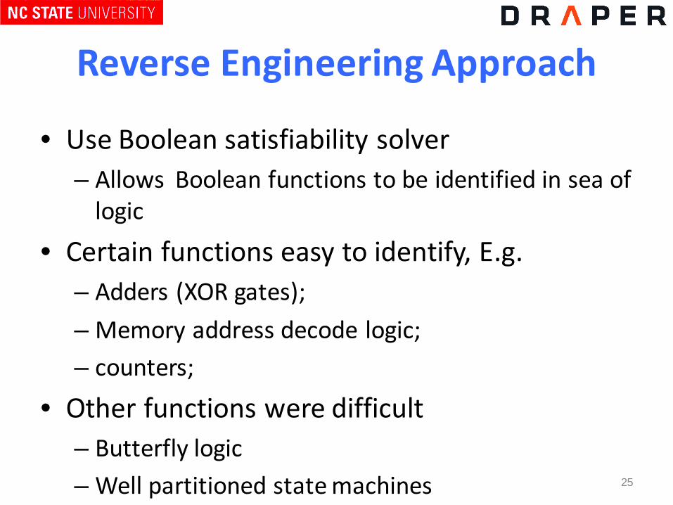
Reverse Engineering Approach
• Use Boolean satisfiability solver– Allows Boolean functions to be identified in sea of
logic
• Certain functions easy to identify, E.g.– Adders (XOR gates); – Memory address decode logic; – counters;
• Other functions were difficult– Butterfly logic– Well partitioned state machines 25
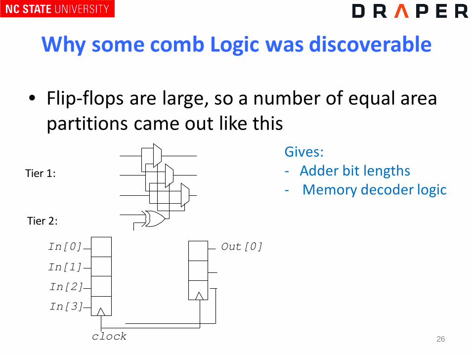
Why some comb Logic was discoverable
• Flip-flops are large, so a number of equal area partitions came out like this
26
In[0]
In[1]
In[2]
In[3]
clock
Out[0]
Tier 1:
Tier 2:
Gives: - Adder bit lengths- Memory decoder logic
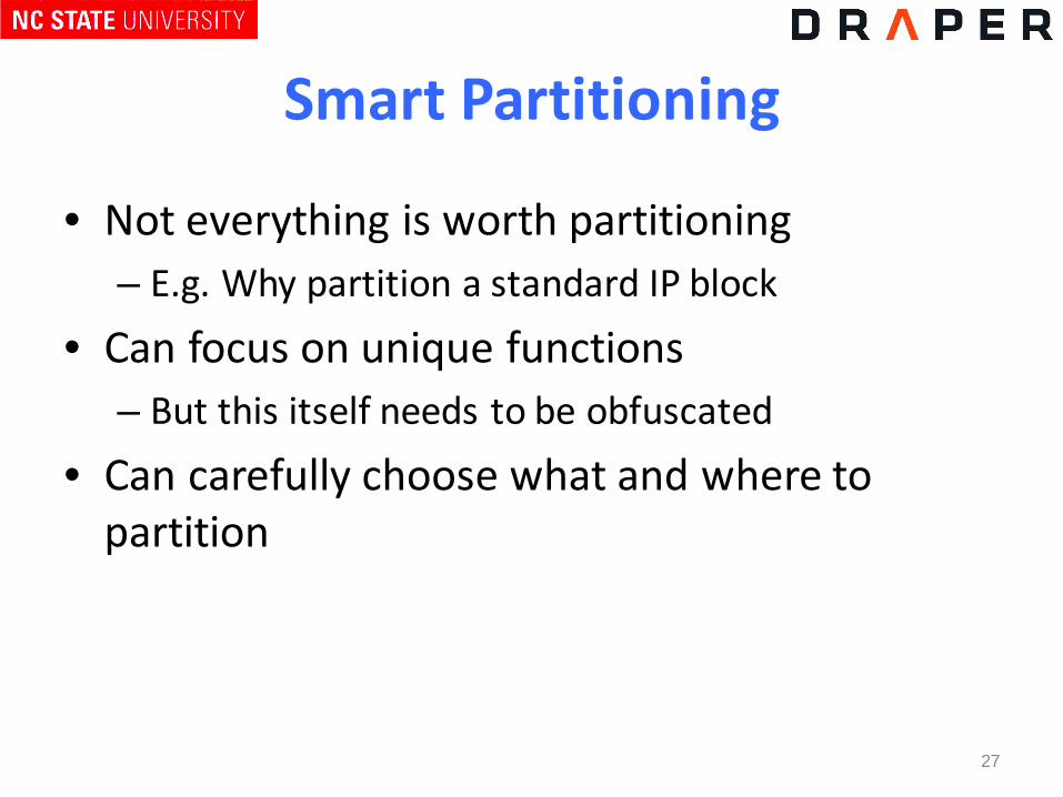
Smart Partitioning
• Not everything is worth partitioning– E.g. Why partition a standard IP block
• Can focus on unique functions– But this itself needs to be obfuscated
• Can carefully choose what and where to partition
27
Smart Partitioning
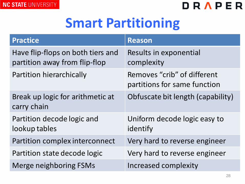
28
Practice ReasonHave flip-flops on both tiers and partition away from flip-flop
Results in exponential complexity
Partition hierarchically Removes “crib” of different partitions for same function
Break up logic for arithmetic at carry chain
Obfuscate bit length (capability)
Partition decode logic and lookup tables
Uniform decode logic easy to identify
Partition complex interconnect Very hard to reverse engineerPartition state decode logic Very hard to reverse engineerMerge neighboring FSMs Increased complexity
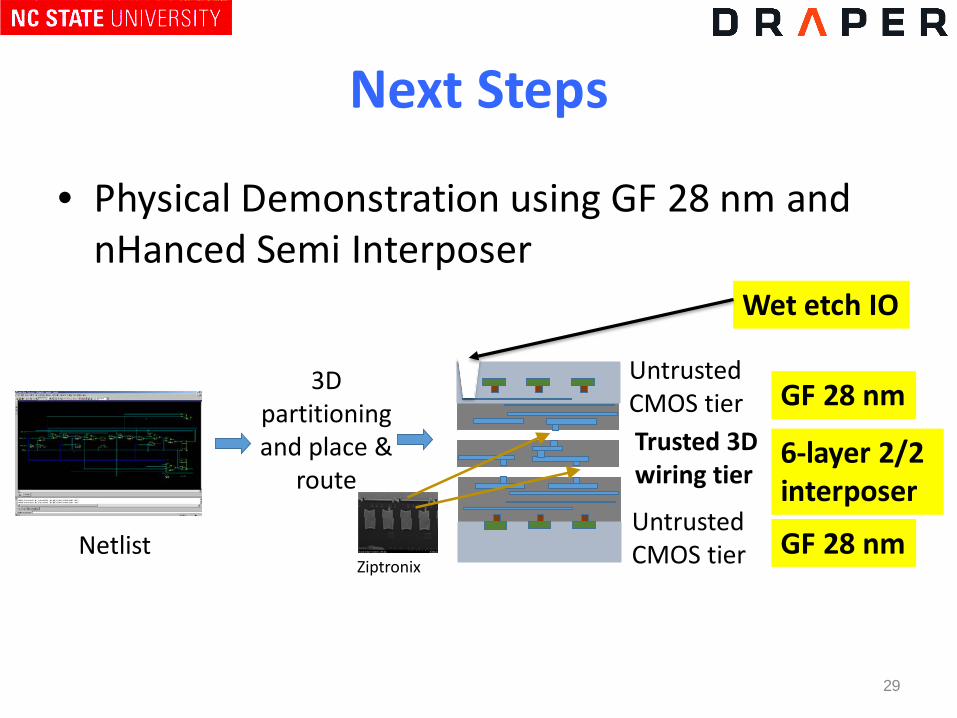
Next Steps
• Physical Demonstration using GF 28 nm and nHanced Semi Interposer
29
Netlist
3D partitioning and place &
route
Untrusted CMOS tier
Untrusted CMOS tier
Trusted 3D wiring tier
Ziptronix
GF 28 nm
GF 28 nm
6-layer 2/2 interposer
Wet etch IO
Next Steps
• Designs to be obfuscated– Arithmetic– Finite State Machines– AES core– SIMD compute core
• December tapeout for September demonstration
30
Conclusions
• 3D partitioning used a trusted routing layer has potential to greatly increase the cost of executing the following threats– Capability discovery with no trusted IC fab– Sophisticated Trojan insertion
• Preliminary experiment confirms netlist complexity– Exponential complexity with non uniform FF or
area assignment
• Building Smart partitioner 31
Acknowledgements
• Funded by Dan Green (DARPA) through ONR
32
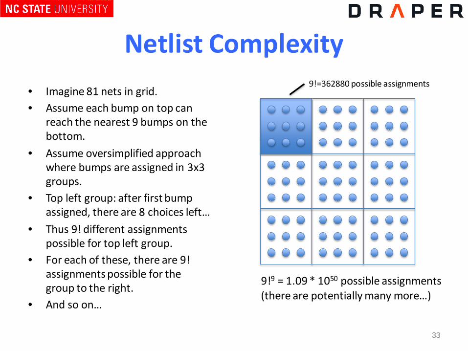
Netlist Complexity• Imagine 81 nets in grid.• Assume each bump on top can
reach the nearest 9 bumps on the bottom.
• Assume oversimplified approach where bumps are assigned in 3x3 groups.
• Top left group: after first bump assigned, there are 8 choices left…
• Thus 9! different assignments possible for top left group.
• For each of these, there are 9! assignments possible for the group to the right.
• And so on…
33
9!=362880 possible assignments
9!9 = 1.09 * 1050 possible assignments(there are potentially many more…)
Next step in Seedling
• Produce new design that1. Assumes a 3D clock router2. Follows “smart partitioning” guidance as much
as practical with current partitioning flow
Hand to red-team for analysis
34
CAD FLOW• Simplified flow:
– synthesis– full 2D PR in area A– partition to TOP and BOTTOM– PR TOP in area A/2
• interposer map created and used to limit f2f bump choices • f2f bumps assigned based on net centroids from 2D design scaled down• placement based on f2f bumps
– PR BOTTOM in area A/2• f2f bumps assigned based on TOP bumps and interposer map• placement based on f2f bumps
– TOP and BOTTOM routed netlists combined for timing analysis– TOP and BOTTOM tweaked as needed
35
Comment #1
• Keeping clock (i.e. flops) within one tier enabled identifying functionality of many logic blocks easy
• Flops take a lot of area so this forces logic into other tier, i.e.
36
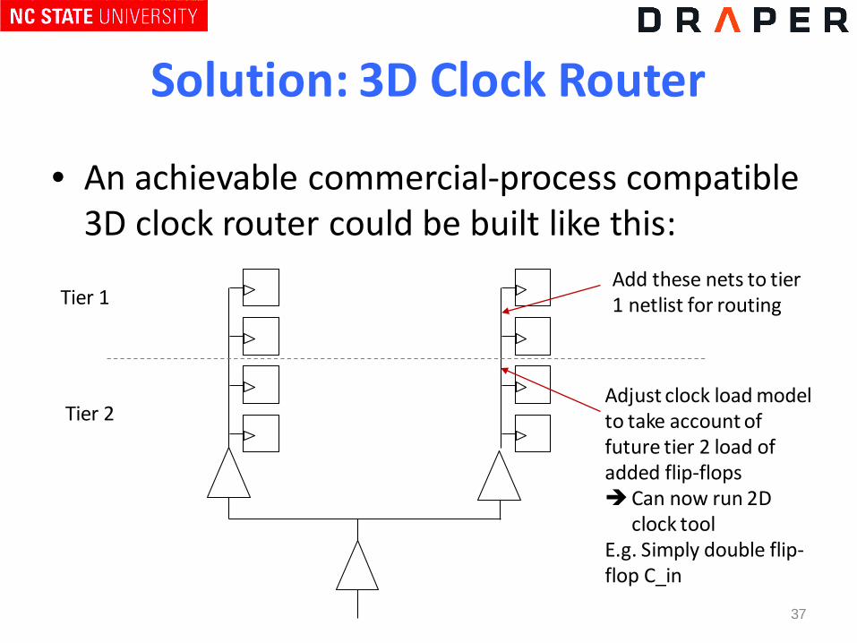
Solution: 3D Clock Router
• An achievable commercial-process compatible 3D clock router could be built like this:
37
Tier 1
Tier 2Adjust clock load modelto take account of future tier 2 load of added flip-flopsCan now run 2D
clock toolE.g. Simply double flip-flop C_in
Add these nets to tier 1 netlist for routing
3D Clock Router
• Other benefits:– Would reduce the number of vertical signal
connections by a factor of two• Only need one per partitioned net, not two
• Metrics improve with fewer partitions needed
38
Comment #2
• Partitioning more effective if more attention given to WHAT and where to partition
• Only partially possible with current Hmetis partitioner
• Could be possible with future “Smart partitioning” tool
39
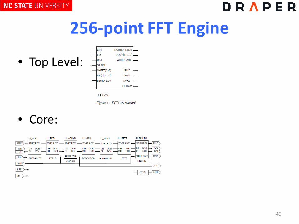
256-point FFT Engine
• Top Level:
• Core:
40
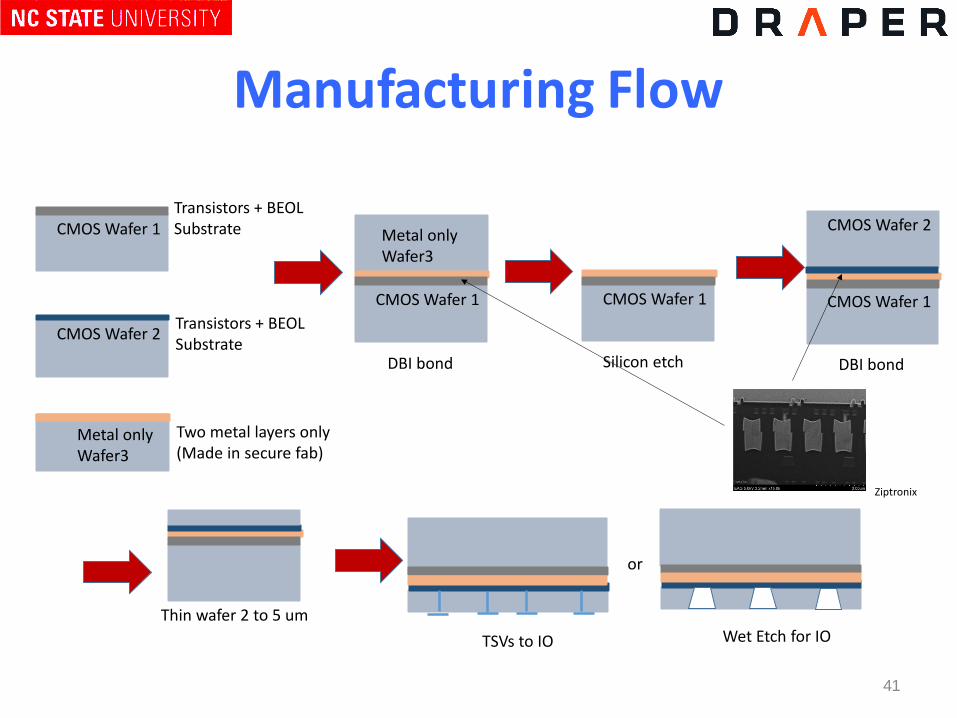
Manufacturing Flow
41
Transistors + BEOLSubstrateCMOS Wafer 1
Transistors + BEOLSubstrateCMOS Wafer 2
Two metal layers only(Made in secure fab)
Metal only Wafer3
Metal only Wafer3
CMOS Wafer 1
DBI bond
CMOS Wafer 1
Silicon etch
CMOS Wafer 1
CMOS Wafer 2
DBI bond
Thin wafer 2 to 5 umWet Etch for IO
or
TSVs to IO
Ziptronix
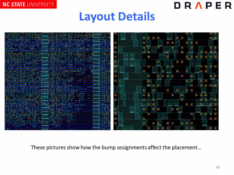
Layout Details
42
These pictures show how the bump assignments affect the placement…
Recommended