U.S. DEPARTMENT OF THE INTERIOR
U.S. GEOLOGICAL SURVEY
The Hawaiian Volcano ObservatoryPolling Telemetry System
For Low Frequency Data Acquisition
by
Gary S. Puniwai1Ken T. Honma1
Allan J. Largo1
Open File Report No. 90-525
This report is preliminary and has not been reviewed for conformity with U.S. Geological Survey editorial standards. Any use of trade, product, or firm names is for descriptive purposes only and does not imply endorsement by the U.S. Government.
1HAWAIIAN VOLCANO OBSERVATORY HAWAII NATIONAL PARK, HI 96718
THE HAWAIIAN VOLCANO OBSERVATORYPOLLING TELEMETRY SYSTEM
FOR LOW FREQUENCY DATA ACQUISITION
CONTENTSPage No
Introduction 3.System Description 4.Control System 7.General Description 8.Apple Interface 10.Radio Interface 16.Radio System 20.Audio Monitor 22.
Remote Field System 24.General Description 25.Electronics Box 27.DTMF Decoder Board 29.Mux & Control Board 35.VCO Board 47.DC Converter Board 51.Motherboard 54.Field Radio System 57.Radio Repeater 60.
Operation 61.References 63.
FIGURES No.1. System Block Diagram 5.2. Control System Diagram 9.3. Apple Interface Schematic 11.4. Apple Interface Timing Diagram 14.5. Apple Interface Layout 15.6. Radio Interface Schematic 18.7. Radio Interface Layout 19.8. Audio Monitor Schematic 23.9. Remote System Pictorial 26.
10. Electronics Box Diagram 28.11. DTMF Decoder Schematic 30.12. DTMF Decoder Layout 34.13. Mux & Control Signal Flow Diagram 36.14. Mux & Control Schematic 38.15. Mux & Control Timing Diagram 40.16. Serial Data Train Diagram 42.17. Mux & Control Layout 46.18. FSK4 VCO Schematic 48.19. FSK4 VCO Programming 49.20. FSK4 VCO Layout 50.21. DC Converter Schematic 52.22. DC Converter Layout 53.23. Motherboard Schematic 55.
continued next page
FIGURES, cont.
24. Motherboard Layout 5625. Radio Box Diagram 58
TABLES
1. Apple Interface Parts List 64,2. Radio Interface Parts List 653. Electronics Box Parts List 664. Electronics Box Pin Designations, I 675. Electronics Box Pin Designations, II 686. DTMF Decoder Parts List 697. Mux & Control Parts List 708. FSK4 VCO Parts List 729. DC Converter Parts List 73
10. Motherboard Parts List 7411. Radio System Parts List and Pin Designation 75
INTRODUCTION
The Hawaiian Volcano Observatory Polling Telemetry System was
designed to replace the "Multichannel Digital Telemetry System"
(Roger, 1976) built by Menlo Park and installed at HVO in the mid
1970's. The old telemetry system was experiencing many problems
due to age and unavailability of more units and parts.
The HVO Polling Telemetry System was designed to meet the
following specifications: 1) must operate on a 12 volt battery, 2)
must have low power consumption, 3) must accept an analog input
range of ±5 volts with 12 bit resolution, 4) must accept at least
8 input channels, and 5) sampling interval must be remotely
controlled. This has been accomplished with the first field units
operating in 1984. By early 1988, the old digital telemetry system
had been completely replaced.
A computer in the observatory controls the data acquisition
or sampling interval from remote stations through 2-way radio
communication. Being an interrogation or polled system, only two
radio frequencies are necessary for the system; one frequency for
simplex (direct) communication and the other frequency for
communicating through a repeater. The design of the system limits
the number of stations to 256, with each station capable of
transmitting data from up to 8 channels. The sampling interval is
set by the computer and ranges from once a minute to once a day.
Data is acquired from sensors only when polled by the computer, so
only low frequency or slowly changing measurements can be usefully
acquired.
SYSTEM DESCRIPTION
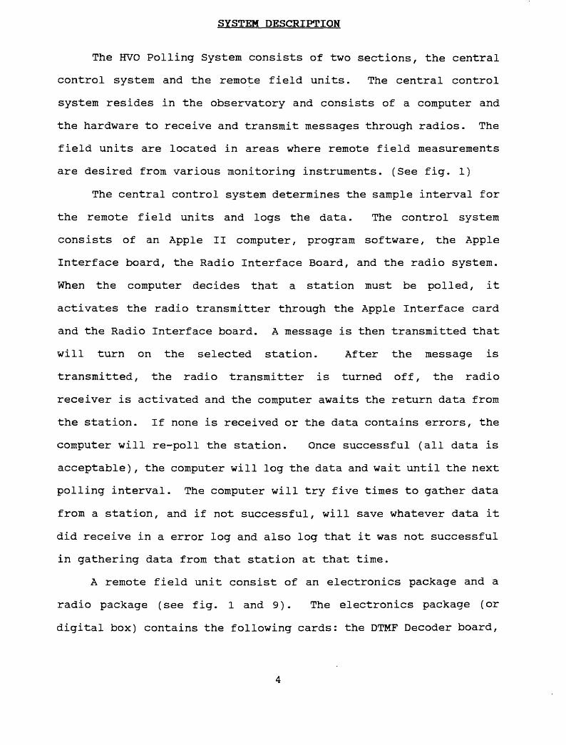
The HVO Polling System consists of two sections, the central
control system and the remote field units. The central control
system resides in the observatory and consists of a computer and
the hardware to receive and transmit messages through radios. The
field units are located in areas where remote field measurements
are desired from various monitoring instruments. (See fig. 1)
The central control system determines the sample interval for
the remote field units and logs the data. The control system
consists of an Apple II computer, program software, the Apple
Interface board, the Radio Interface Board, and the radio system.
When the computer decides that a station must be polled, it
activates the radio transmitter through the Apple Interface card
and the Radio Interface board. A message is then transmitted that
will turn on the selected station. After the message is
transmitted, the radio transmitter is turned off, the radio
receiver is activated and the computer awaits the return data from
the station. If none is received or the data contains errors, the
computer will re-poll the station. Once successful (all data is
acceptable) , the computer will log the data and wait until the next
polling interval. The computer will try five times to gather data
from a station, and if not successful, will save whatever data it
did receive in a error log and also log that it was not successful
in gathering data from that station at that time.
A remote field unit consist of an electronics package and a
radio package (see fig. 1 and 9). The electronics package (or
digital box) contains the following cards: the DTMF Decoder board,
REMOTEFIELDSYSTEM
DTMF
MUX
FSK
DC C.
ELECTRONICS BOX
CENTRAL CONTROL SYSTEM
CENTRAL COMPUTER
SYSTEM BLOCK DIAGRAM
FIG. 1
the MUX & CONTROL board, the DC Converter board, the FSK board, and
the Motherboard. The radio container holds the radio transceiver.
The remote field units are always on standby, awaiting a call from
the controlling computer. Whenever it detects calling, it compares
the message it receives with its own programming. If there is a
match, it will power up, transmit its data, then return to standby.
If there is no match, it will ignore the call and stay on standby.
The radio receiver is always on during standby. When the station
powers up, the transmitter is activated so that the station can
transmit the data to the computer.
The remainder of this report describes each of the compo
nents of the system, the design and operation of the circuit,
with a schematic and parts layout diagram.
This report is meant to provide a system description and a
reference for repair and operation of the equipment designed by
the authors, and as such will not discuss the operation and re
quirements of the Apple Computer and its software. Operation and
questions concerning the computer should refer to USGS open file
report no. 87-633, (English, 1987).
THE CONTROL SYSTEM GENERAL DESCRIPTION
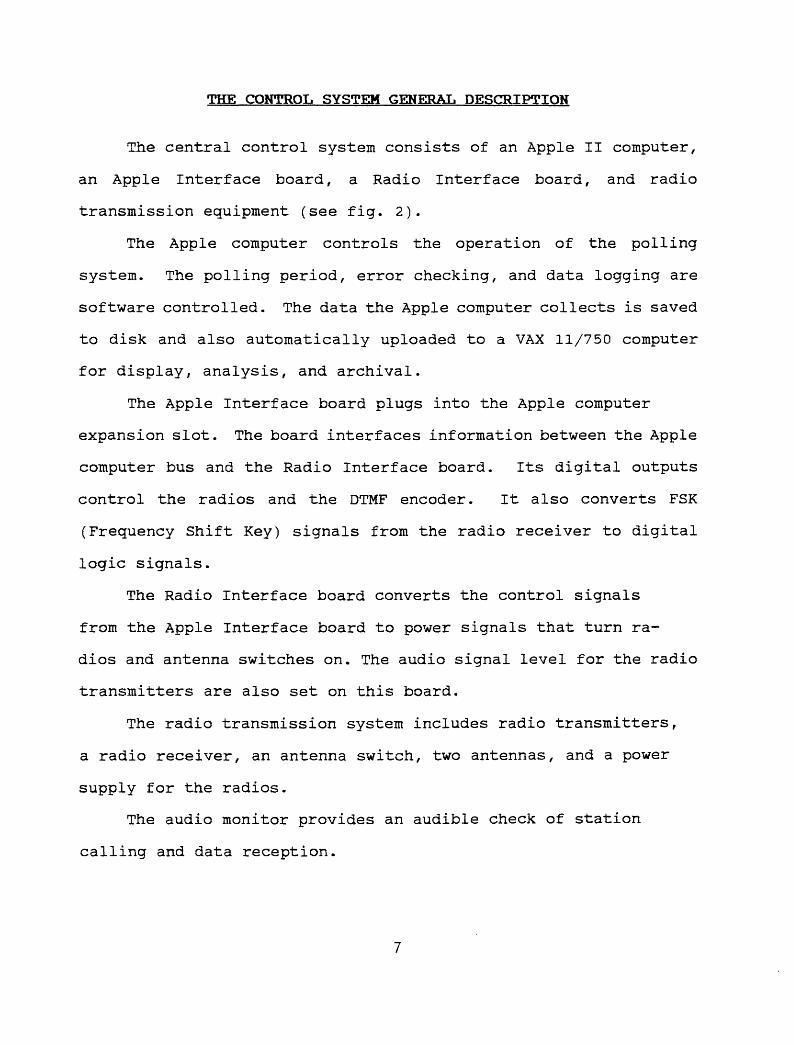
The central control system consists of an Apple II computer,
an Apple Interface board, a Radio Interface board, and radio
transmission equipment (see fig. 2).
The Apple computer controls the operation of the polling
system. The polling period, error checking, and data logging are
software controlled. The data the Apple computer collects is saved
to disk and also automatically uploaded to a VAX 11/750 computer
for display, analysis, and archival.
The Apple Interface board plugs into the Apple computer
expansion slot. The board interfaces information between the Apple
computer bus and the Radio Interface board. Its digital outputs
control the radios and the DTMF encoder. It also converts FSK
(Frequency Shift Key) signals from the radio receiver to digital
logic signals.
The Radio Interface board converts the control signals
from the Apple Interface board to power signals that turn ra
dios and antenna switches on. The audio signal level for the radio
transmitters are also set on this board.
The radio transmission system includes radio transmitters,
a radio receiver, an antenna switch, two antennas, and a power
supply for the radios.
The audio monitor provides an audible check of station
calling and data reception.
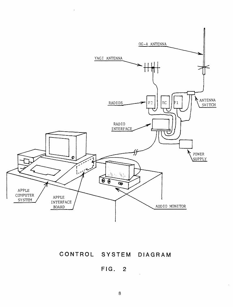
OG-4 ANTENNA
YAGI ANTENNA
APPLE COMPUTER SYSTEM
APPLE INTERFACE BOARD
CONTROL SYSTEM DIAGRAM
FIG. 2
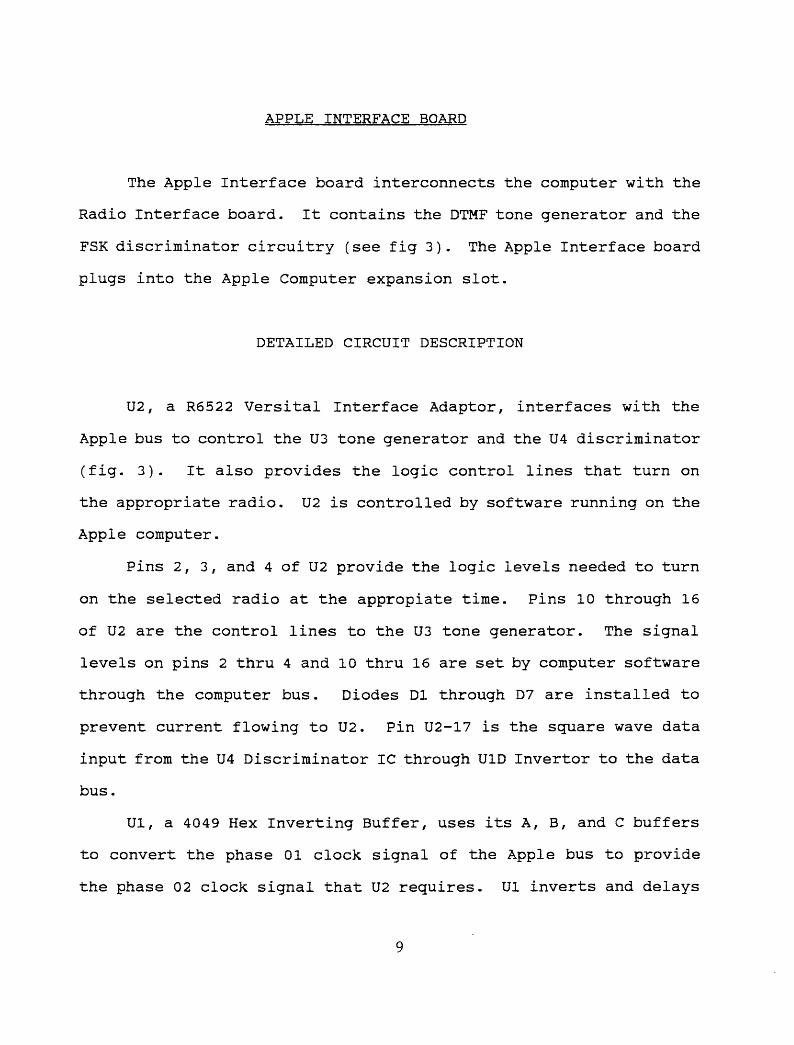
APPLE INTERFACE BOARD
The Apple Interface board interconnects the computer with the
Radio Interface board. It contains the DTMF tone generator and the
FSK discriminator circuitry (see fig 3). The Apple Interface board
plugs into the Apple Computer expansion slot.
DETAILED CIRCUIT DESCRIPTION
U2, a R6522 Versital Interface Adaptor, interfaces with the
Apple bus to control the U3 tone generator and the U4 discriminator
(fig. 3). It also provides the logic control lines that turn on
the appropriate radio. U2 is controlled by software running on the
Apple computer.
Pins 2, 3, and 4 of U2 provide the logic levels needed to turn
on the selected radio at the appropiate time. Pins 10 through 16
of U2 are the control lines to the U3 tone generator. The signal
levels on pins 2 thru 4 and 10 thru 16 are set by computer software
through the computer bus. Diodes Dl through D7 are installed to
prevent current flowing to U2. Pin U2-17 is the square wave data
input from the U4 Discriminator 1C through U1D Invertor to the data
bus.
Ul, a 4049 Hex Inverting Buffer, uses its A, B, and C buffers
to convert the phase 01 clock signal of the Apple bus to provide
the phase 02 clock signal that U2 requires. Ul inverts and delays

CO
MP
UT
BU
SS
01 m
h
+5V
25-
*
* '
C.*
J
-R/U
,1
8-
*' "
^iR
ES
3
1.-
HJ
JA
2 "3
"n
w
~
__
AI
"o"
,,^1
,;«
.2-
AQ
T
*T
O
D7
42
- D
6 4
3-
D3
44 -
co
D4 fi-
D3
46-
D2
47
Dl
48
-D
0 4
9-
i K
M j
«jig
|
+ lg
V(5
0f-
11 \f*
-
JET
20
/24
-* S
H
23
34 35
36
37 38 26 27
28
29 30 31 32
33
1 1 1
?
vU
1
4049
t
C
B
L6
n
5{^
_4
r c
T
, , |j_
l'4
.7K
I !0
Pf
i !
1
02
D0
Dl
D2
pg
D3
D4
U2
D5^^
D6
D7
R6522
P1
D0
Dl
D2
21
3r-
?
2 R
1
^~
IK
< ,
R2
j: 4.7
K
25
1.1
18
hi
Ul
H
Rl
Vd
011
bll
KJI
D2
13
R1
°
~1
2
Mr
Kfl
D3
12
R2
S2559A
13
M?
4
^'
U
R4
0 i
14
Ml
KjiD
S
3 R
4 rn
l
15
Ml
KflD
6 4
«16
N
ID7
Ml
5 C
2 C
4n?
W
K ' c
3 OT
VsU
l "
«15
_^1
1
4
0-
1H
I __
R4
3
( i \w
^
. 3K
Re
F2
Fl
DTM
F
AP
PL
E
INT
ER
EA
I
DR
AU
N
GP
8-2
5-8
8
DE
SIG
NE
D
GP
S. K
H
11
-8
UN
LES
S
NO
TE
D/
1.
RE
SIS
TO
RS
5H
, lx
4U
2.
RE
SIS
TO
R
R7
= 2*
3.
CA
PA
CIT
OR
S
AR
E
CE
RA
MIC
4.
CA
PA
CIT
OR
C
3 IS
P
OLY
CA
RB
ON
AT
E
5.
DIS
CR
IMIN
AT
OR
S
PE
CS
H
I:
2200H
Z
LO:
1200H
Z
CF
: 1
70
0H
Z
RA
TE
: 6
00
BP
S
6.
DIO
DE
S
AR
E
1N
91
4
)3
R
5 7
IBM
Y
l '
J 1
3.5
8M
HZ
IS
C
3 U
4
* 1
1 -n
?2
2u
f X
R2211
^i
Hh
R?
9 C
4 ""
L
3
20K
_ i,
fl.J
uf
14
I
1J
r-^V
V
?-._
.,_
nn
10
T T
2^ J
4 R
IN
TO-*
/
R6H
*t
K
M.
S-
is: i
iv
:s 'T
E T
Vs
Tc 7
1
1 PP
lu
f p=
L
vd
LP 1
1 1_
J(L£
17
8
R
8 ]
«tr
.8(
"--
OT
CM
P l-^
vgpJ
.
Ri0
, R9
In
n nn
, H
^W
-* V
A^ *-j 9
5.
IK
51
0K
««
««
.S
p«?
i f
«.
- -
. 0047u f
-
01
[OCM
:E
SC
HE
MA
TIC
\ R
ll
>
5K
13
32uf
«=
»0.1
uf
, R
12S
uf
*.
5K
^1 60^
I
I^TSS
^
FS
K
FS
K
AP
PLE
IN
TE
RF
AC
EH
VO
IN
TE
RR
OG
AT
ION
S
YS
TE
M<3
the 01 clock signal by 80 nanoseconds to produce a simulated 02
clock signal. Ul-D inverts the output of U4 before sending the
signal on to U2.
U3, a AMI S2559A DTMF Tone generator, produces the tones
necessary to activate the remote field units. U3 is controlled by
U2, which provides the logic level patterns on the row inputs (pins
11 thru 14) and the column inputs (pins 3 thru 5) similar to a
telephone keypad. The output level of U3-16, is 440 to 800 mVrms.
It is sent to the Radio Interface board through the Jl connector.
DTMF (Dual-Tone-Multiple-Frequency) is the system that "touch-
tone" phones use when dialing. When a key on the telephone is
depressed two tones are produced, one signifying the row and one
signifying the column. With each key having two indentifing tones,
the chance for random noise to produce false coding is greatly
reduced.
U4, an Exar XR2211 FSK Demodulator, converts the FSK audio
input into a corresponding square wave signal. The mark/space
frequencies are 1200 and 2200 Hz, with a center frequency of 1700
Hz. The input level to U4 is set by adjusting R12, while Rll is
to fine tune the frequency. U4-7, the discriminator square wave
output, is inverted by Ul-D before entering U2 and the computer
bus.
The FSK input to the Apple Interface board, U4-2, is trans
former coupled by Tl to the radio receiver. This eliminates any
ground loop problems if the radios are located at a distance from
the computer.
ii
The Jl connector connects the signals from this board to the
Radio Interface board.
Figure 4 shows a typical timing sequence of activating radios,
calling a station, and receiving a return signal.
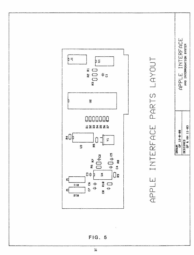
Figure 5 displays the parts layout for the Apple Interface
board.
Table 1 is the Apple Interface Parts List.
12

SIGNAL LOCATION
U2-4
U2-2
U2-3
U3-1S ttff"
U2-I7
U2-10 f|
U2-11 []
U2-12
U2-13 nnU2-14
U2-15 []j]j]
U2-16 (!
0 1
DESCRIPTION
RECEIVER
F1 PWR
F2 PWR
DTMF TONE
mini! SERIAL ir
ROW 1
ROW 2
ROW 3
ROW 4
COLUMN 1
COLUMN 2
COLUMN 3
1
2 3
PWR
IS
JPUT
TIME IN SECONDS
NOTE: 1. TIMING DIAGRAM DEPICTS CALLING STATION #025, TRANSMITTER F1 2. VOLTAGE LEUELS ARE 0 TO 5 VOLTS
APPLE INTERFACE TIMING DIAGRAM
FIG. 4
13
TI O 01
CVJ
1
(
n C7 _L
T
:R
= C6 j_ T
P1
C k
P
*
T i F
C3
LJ U4
J-
?9
U3
R6
P7
K«. r
^D-c
=T
M
T
C4
R8
)^
J
R4
C
LJ-
L_
L
Yl
> >
Dl
iJ_
J-D
2 C
D-
Do
f\ l.
uj
iJ r
D4
{D
D
5 {H
D
DS
{O
D
7 d}-
U2
R2
Rl
R3OD
DHF
-C
l
.11 i >
ui
APPLE INTERFACE PARTS LAYOUT
DRAU
M GP 12
-8-8
8
DESI
GNED
GP
«, KH
11-83
APPLE INTERFACE
HVO
INTERROGATION
SYSTEM
RADIO INTERFACE BOARD
The Radio Interface Board connects the Apple interface
board with the radios. The board is designed to control two radio
transmitters, one radio receiver, and an antenna switch. All
connections concerning power and audio signals to the radios come
from this board.
CIRCUIT DESCRIPTION
The three circuits controlling the radios on this board are
similiar. Because one description is sufficient the F2 radio
circuit will be used. See Fig 6, Radio Interface Schematic. A high
logic level on the F2 Trigger (+5V) from the Apple Interface board
turns on Q4, a MPSA14 NPN Darlington transistor. When the Q4
conducts, it turns on Q3, a 2N4403 PNP general purpose switch,
which then provides power to the radio. The 2N4403 can provide up
to 150 ma at 12V to the radio.
The DTMF signal is sent to the two transmitters through a 5K
pot (R5), which is used to adjust the signal level. The DTMF level
is typically set at 1 volt peak-peak.
The FSK signal from the radio receiver is routed through the
board for easier troubleshooting. The FSK level, also set at 1
volt peak-peak, is set with the receiver output adjustment on the
radio.
To reduce the number of antennas from three to two, an antenna
switch was added to the system. The antenna coaxial switch
15
switches the antenna between the radio receiver and the Fl radio
transmitter. The antenna switch is activated when Fl is powered,
allowing Fl to transmit out of the same antenna used by the radio
receiver.
The current requirements of the coaxial switch could not be
met by a 2N4403, so a 2N5976 is used for Ql. Ql supplies power
for both the antenna switch and the Fl transmitter. When the Fl
trigger is turned on, the Fl radio transmitter is powered up and
the antenna switch switches to connect the transmitter to the
antenna. When the Ql (2N5976) turns off, the Fl transmitter shuts
down and the coaxial switch releases, reconnecting the antenna to
the receiver. The 2N5976 transistor can provide up to 2 amps of
current.
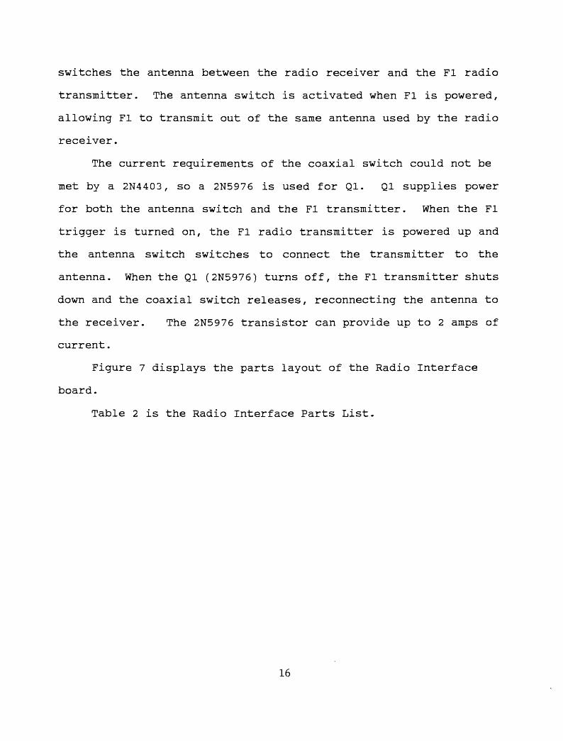
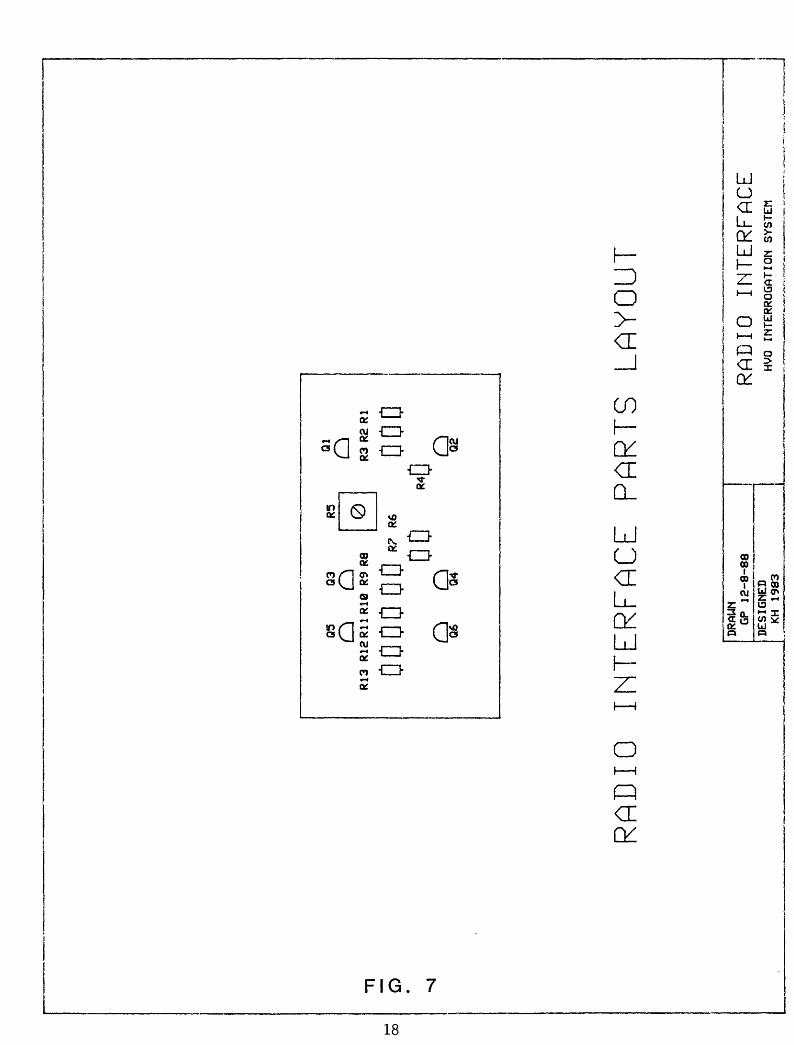
Figure 7 displays the parts layout of the Radio Interface
board.
Table 2 is the Radio Interface Parts List.
16
T1
O
CD
POWER
SUPPLY
FROM
Jl APPLE
INTERFACE
DTM
F
F2
TR
IGG
ER
RC
T
RIG
GE
R
FSK
fil
l
+ 12
V
TO
RA
DIO
S
Fl
RA
DIO
TRANSMITTER
F2 RADIO
TRANSMITTER
51 +V
RADIO
-v RECEIVER
L13
SIG
RADIO INTERFACE SCHEMATIC
| j
: CA
RD EDGE CONNECTOR
t, PIN
NO.
DRAU
MGP
12-8-88
DESIGNED
KH 19
83
RADIO INTERFACE
HVO INTERROGATION SYSTEM
oop -J
R13 D
Q5 o
03
R
3 jij
0R
12R
11R
10
R9
R8
*
ODD
Q 06
QO *
«DD
Q Q4
L-J
*
R3
R2
DDR
4Q
Q
Rl D
RADIO INTERFACE PARTS LAYOUT
DRAW
NGP
12-8-88
DESI
GNED
KH
1983
RADIO INTERFACE
HVO
INTERROGATION
SYSTEM
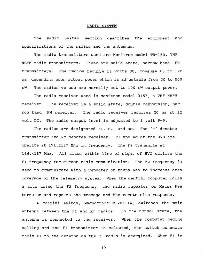
RADIO SYSTEM
The Radio System section describes the equipment and
specifications of the radios and the antennas.
The radio transmitters used are Monitron model TR-150, VHF
NBFM radio transmitters. These are solid state, narrow band, FM
transmitters. The radios require 12 volts DC, consume 60 to 120
ma, depending upon output power which is adjustable from 50 to 500
mW. The radios we use are normally set to 100 mW output power.
The radio receiver used is Monitron model R15F, a VHF NBFM
receiver. The receiver is a solid state, double-conversion, nar
row band, FM receiver. The radio receiver requires 20 ma at 12
volt DC. The audio output level is adjusted to 1 volt P-P.
The radios are designated Fl, F2, and Re. The 'F' denotes
transmitter and Re denotes receiver. Fl and Re at the HVO are
operate at 171.2187 Mhz in frequency. The F2 transmits at
166.4187 Mhz. All sites within line of sight of HVO utilize the
Fl frequency for direct radio communication. The F2 frequency is
used to communicate with a repeater on Mauna Kea to increase area
coverage of the telemetry system. When the central computer calls
a site using the F2 frequency, the radio repeater on Mauna Kea
turns on and repeats the message and the remote site response.
A coaxial switch, Magnacraft W120X-14, switches the main
antenna between the Fl and Re radios. In the normal state, the
antenna is connected to the receiver. When the computer begins
calling and the Fl transmitter is selected, the switch connects
radio Fl to the antenna as the Fl radio is energized. When Fl is
19
shut down, the switch releases and reconnects the antenna to Re.
This switch requires 12 volts and 1.4 watts of power to operate.
Two antennas are used for radio communication. The main
antenna is a Scala OG-4, an omni directional, vertically polar-
zed antenna with 4 db gain. The OG-4 is connected to the coax
ial switch for use with the Fl and Re radios. The OG-4 is used
for all radio reception from field stations. The second antenna
is a Scala CA5-150V, a vertically polarized antenna with 9db gain.
This antenna is only used when the F2 radio transmits, and is aimed
at the radio repeater site on Mauna Kea.
The radios and switch require a 12 volt power supply that can
provide a minimum of 500 ma. With the Fl radio transmitting
and the antenna switch activated, current consumption is measured
at 250 ma.
20
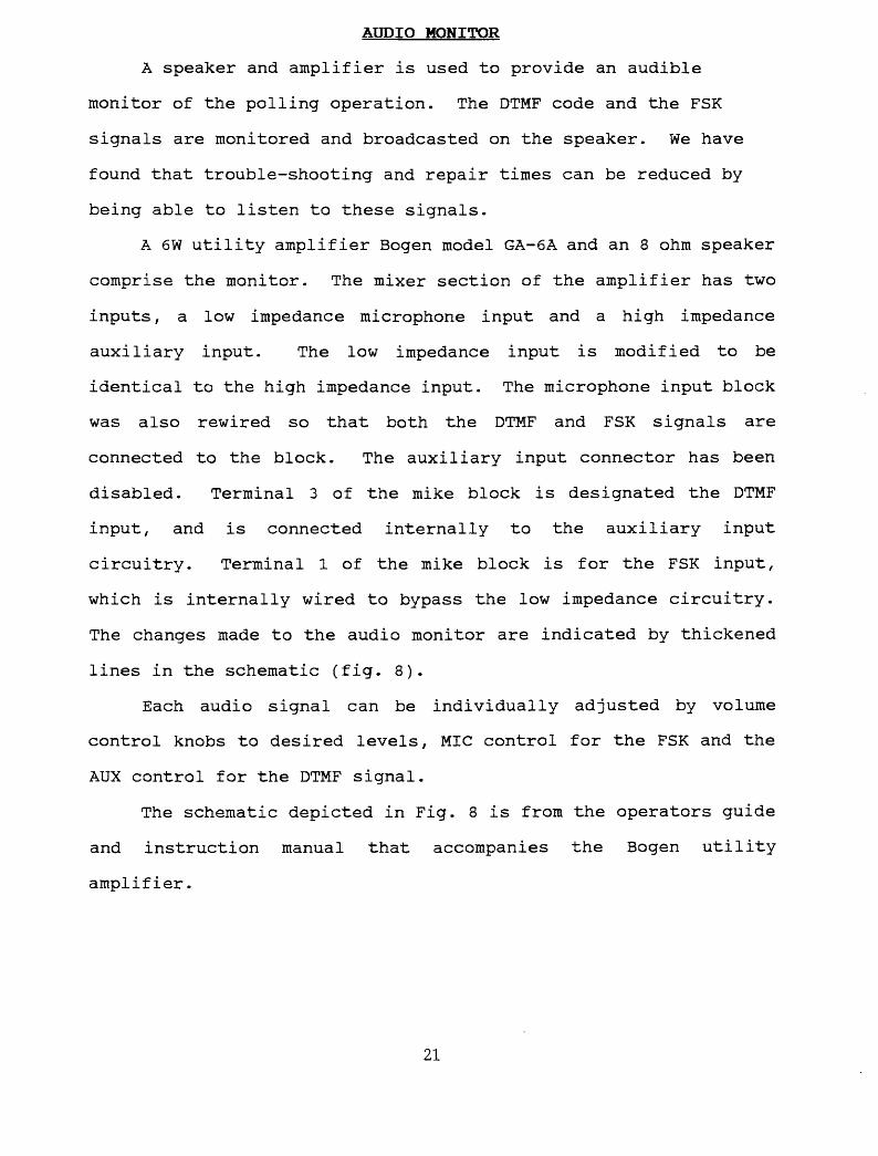
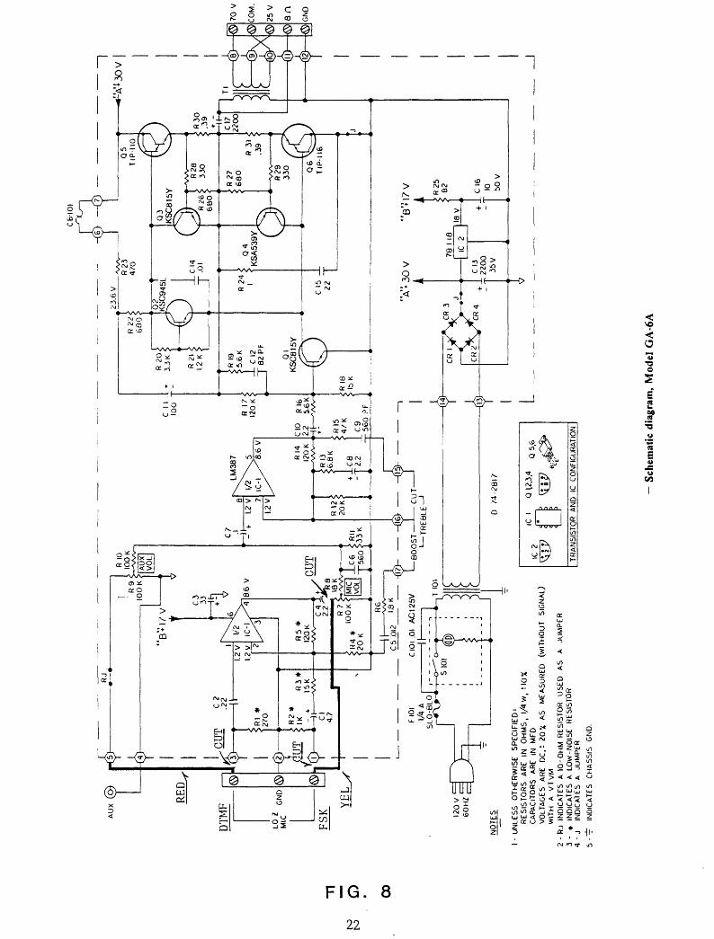
AUDIO MONITOR
A speaker and amplifier is used to provide an audible
monitor of the polling operation. The DTMF code and the FSK
signals are monitored and broadcasted on the speaker. We have
found that trouble-shooting and repair times can be reduced by
being able to listen to these signals.
A 6W utility amplifier Bogen model GA-6A and an 8 ohm speaker
comprise the monitor. The mixer section of the amplifier has two
inputs, a low impedance microphone input and a high impedance
auxiliary input. The low impedance input is modified to be
identical to the high impedance input. The microphone input block
was also rewired so that both the DTMF and FSK signals are
connected to the block. The auxiliary input connector has been
disabled. Terminal 3 of the mike block is designated the DTMF
input, and is connected internally to the auxiliary input
circuitry. Terminal 1 of the mike block is for the FSK input,
which is internally wired to bypass the low impedance circuitry.
The changes made to the audio monitor are indicated by thickened
lines in the schematic (fig. 8).
Each audio signal can be individually adjusted by volume
control knobs to desired levels, MIC control for the FSK and the
AUX control for the DTMF signal.
The schematic depicted in Fig. 8 is from the operators guide
and instruction manual that accompanies the Bogen utility
amplifier.
21
CB
-IOI
T|
0 00
05
TIP
-110
^\
-A"
30V
120V
60
HZ
NO
TES
1-U
NLE
SS
O
THE
RW
ISE
S
PE
CIF
IED
'R
ES
ISTO
RS
A
RE
IN
O
HM
S,
I/4
W,
*IO
%C
AP
AC
ITO
RS
AR
E IN
M
FDV
OLT
AG
ES
AR
E D
C,-
20X
A
S
ME
AS
UR
ED
(W
ITH
OU
T S
IGN
AL)
WIT
H
A V
TV
M2
- R
J IN
DIC
ATE
S
A 1
0-O
HM
RE
SIS
TOR
U
SE
D
AS
A
JU
MP
ER
3 -
*
IND
ICA
TES
A
LOW
-NO
ISE
R
ES
ISTO
R4
- J
IND
ICAT
ES
A JU
MP
ER
5-^
IND
ICA
TES
C
HA
SS
IS
GN
D.
Sche
mat
ic d
iagr
am,
Mod
el G
A-6
A
REMOTE FIOT.n SYSTEM GENERAL DESCRIPTION
The remote field system consists of two packages: the el
ectronics package, the radio package; and external pieces such as
batteries, masts, and antennas. The electronics package consists
of several circuit boards which handle site activation and data
transmission. The radio system includes the radio package,
cables, and antenna with masts. See fig. 9.
23
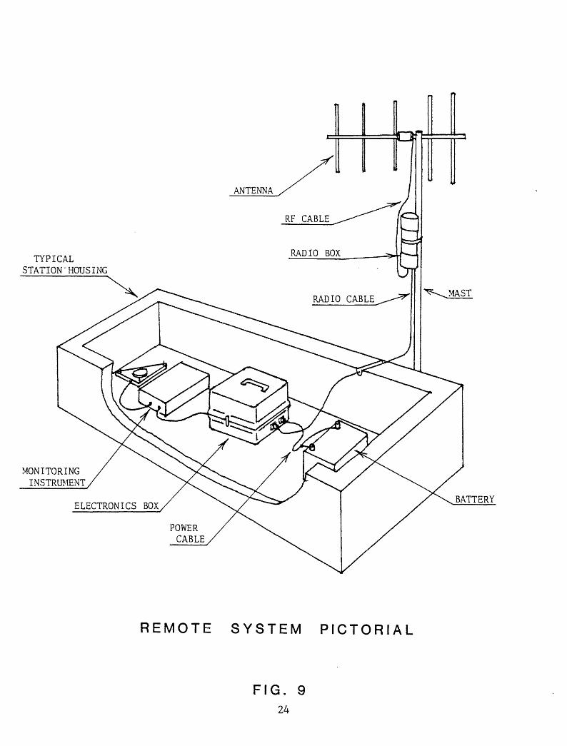
TYPICAL STATION"HOUSING
MONITORING INSTRUMENT
ELECTRONICS BOX
REMOTE SYSTEM PICTORIAL
FIG. 924
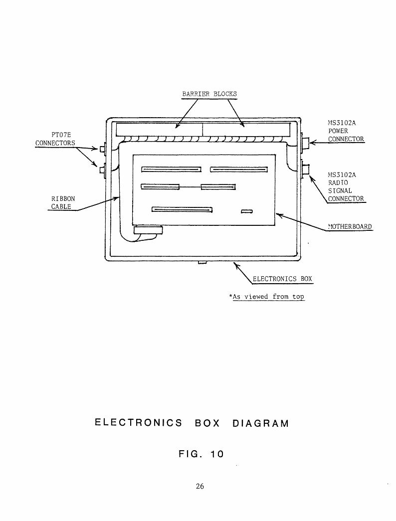
THE ELECTRONICS PACKAGE
The electronics package (or digital box) contains and protects
the following boards: l)the DTMF Decoder board that controls the
powering up a station by comparing its programming with that sent
by the central computer, 2)the Mux & Control board that handles
the power switching, data digitization, and data formatting, 3)
the DC Converter that converts the battery voltage to the voltages
required by the digital box, 4)the FSK4 VCO that converts the data
from the Mux & Control board to one that is acceptable by the
radios, and 5)the Motherboard that holds the above boards and
interconnects them (fig. 10). Each board will be discussed in
detail in following sections.
Connectors are mounted on the electronics box to allow easy
connection of power and signals. An MS3102A-14S-9S bulkhead
connector is used as the power input for the remote field system.
An MS3102A-14S-5S is used for all power and signals to and from
the radio box. A Bendix PT07E-8-4P is used for all instrument
signals entering the electronics box. Two barrier terminal blocks,
Cinch 10-14Q-Y, are mounted inside the electronics box. All
cables, such as power, signal, and ribbon are connected to the
barrier block. A Digikey R505-36-ND ribbon cable with a card end
connector that plugs onto the motherboard transfers all signals and
power between the motherboard and the barrier blocks. These
connectors allow easy replacement of components, and the barrier
blocks allow easy checking of all signals and power systems. See
Tables 4 & 5 for pin designations.
25
PT07E CONNECTORS
RIBBON CABLE
BARRIER BLOCKS
} J J J J J J J J } J J ) } J J ) J J )<r
MS3102APOWERCONNECTOR
MS3102A RADIO SIGNAL .CONNECTOR
MOTHERBOARD
ELECTRONICS BOX
*As viewed from top
ELECTRONICS BOX DIAGRAM
FIG. 10
26
DTMF DECODER BOARD
GENERAL DESCRIPTION
The DTMF (Dual-Tone-Multiple-Frequency) Decoder board mon
itors the radio receiver audio output for the correct code se
quence that will tell it to turn on the station. The board
compares the codes that it detects with its own programming. If
it detects a match, it sends the power up signals to the Mux &
Control board.
The DTMF code format was chosen for its ease in application,
wide product selection, and high resistance to noise interfer
ence. The DTMF (commonly known as Touch Tone) was developed by
telephone companies as a more rapid and accurate means of dialing.
Each key on a push-button telephone, when depressed, causes two
specified tones to be transmitted. A DTMF decoder can easily
identify when valid tones are transmitted, and which key was
activated.
The central control computer first transmits a reset tone,
then the three number code that activates the station to be polled.
The reset tone is transmitted first to clear any number that may
have spuriously activated part of the decoder board.
The DTMF board can decode the numbers 0 thru 9 plus the '#'
and '*' characters. The '#' and '*' characters are reserved for
board resetting. The decoder requires a minimum of 20 millise
conds to identify a character with a minimum of 10 milliseconds
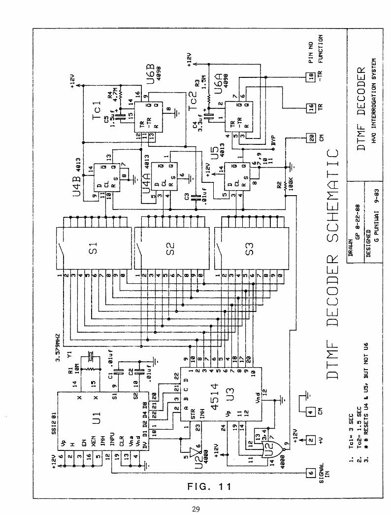
between characters. Dipswitchs SI, S2, and S3 (see fig. 11) are
set sequencially to match the station identification number. There
are two timers on board, the first with a 3 second timeout and the
27
second with a 1.5 second timeout. The first timer starts upon
detection of the first number that is received and will then reset
the card in three seconds. This is to take care of any spurious
noise that may have triggered the station, and long enough to allow
hand DTMF triggering of the card. The second timer, activated
after a valid three number tone sequence is received, sets a low
logic level which causes the digital system to power up. After
allowing 1.5 seconds for components to stabilize, a change to a
high logic level will initiate the digitization and data
transmission.
DETAILED CIRCUIT DESCRIPTION
Ul is a SSI201 DTMF decoder capable of decoding 0 thru 9, A
thru D, and the characters * and #. See Fig. 11. The input signal
to Ul-12 must be between 10 and 3000mv RMS. The output is a four
line hexadecimal code on pins 1, 22, 21, and 20. Ul-18 signals a
valid tone detection by going high.
U3 is a 4514, a 4 to 16 line decoder, which translates the
four line hexadecimal code to one of 16 single output lines. Of
these 16 output lines only 12 are used. Code outputs 1 thru 10 are
sent to the three programming switches SI, S2, and S3. Code
outputs 11 and 12, signifying '*' and '#', are sent to U2-11 and
12 for use in resetting the board. U2 is a 4001 dual NOR gate with
inverter. The inverter of U2, pins 5 and 6, inverts the strobe
line from Ul-18 to U3-23. U3-23 is the inhibit line, and must be
low when U3 is converting. The U2 NOR gate input pins 11 and 12
take the # and * characters from U3 thru the NOR gate to trigger
the reset lines of U4 and U5.
28
SSI201
toTl o S
IGNAL
IN
1.
Tcl= 3
SEC
2.
Tc2= 1.
5 SEC
3.
* # RESETS U4
US/
BUT NOT U6
1 2 3
i <
<
4
<
L
5
i <
i
6
~
7
i 111 <l
_
8
<
9
» <
0 1 2 3 4 5 6 7 8 9 1 2 3 4 5k
6I
7 8 9 0
^*
SI
^^
S2
^^
S3
DE
CO
DE
<
i
i
i
i i
<
i
<
< t> > > i i > t * * i i ,
<
k > <
i * i
U4B
401
3 n
f 14
^r s
10
CL
13R
s a
,lJ
7
-
U4A
401
3Jij
5 Q
CL
° j
~
R
s Q
6"-
J,
Jlfl nil
01u
f .1
2V
i
4 LJ
5 i
LJ o
^ 11
4 40
1:
Te
lC
5 rJIV
^^
1 15
1
14
12
TR
161
" 9
1 !^
D13
^
' "^
^ U
D J
jR
Q 4
09
8
8
C4
Tc2 p
^ t,
3.3
uf
**
, Hn
*0
,,,,
Jl
T
a i
« U
6Aa
_ 4
«»W
^B
0 D
_ ^^
- ri
Q
1 J
R s
Qj "7/9
10
o R
2
100K
--
R S
CH
EM
AT
ICD
RA
UN
GP
8-2
2-8
8
-p
DE
SIG
NE
D
G P
UN
IUA
I 9-8
3
5 Ir
i 7
3 :TR
s «
i
R Q
BYP 20
16
18
P
IN
NO
CM
TR
-TR
FU
NC
TIO
N
IMF
D
EC
OD
ER
HVO
IN
TER
RO
GA
TIO
N
SY
STE
M

U4 and U5 are 4013 flip flops, used to convert voltage lev
els from U3 and the switches into pulses that can trigger the ti
mers of U6. The components of the 4013's are cascaded to allow
triggering only in the programmed sequence. The first decoded
number from U3 passing if it is selected thru SI sets U4B which
sets both U6A, the 3 second timer (Tel), and U4A. U4A, after being
set by U4B and then triggered by the second coded number passing
thru S2, sets USA. U5A, after being set by U4B and then being
triggered by the third station number matching S3, triggers U6A
(Tc2) the 1.5 second timer. This section was designed so that
numbers transmitted only in the correct sequence would be able to
set the flip flops. The flip flops will not set Tc2 unless they
are activated in the correct sequence. The setting of switches SI,
S2, and S3 are covered in the Operation section, page 62.
U6, a 4098, is a dual monostable multivibrator. Section
U6B handles the 3 second timer (Tel) and section U6A handles the
1.5 second timer. (Tc2). The U6B timer is set by U4B when a number
matching SI is detected, whether from noise or from actual computer
activation. After Tel times out in 3 seconds, the Q of U6B will
reset U4 and U5. This timer is set with a long time constant to
allow hand DTMF triggering of the board, which takes longer than
computer calling.
The Q output of section U6A provides the high logic level (TR)
for station powerup and the Q of section U6A provides another high
logic level (TR) to start data digitization. The TR and the TR
from U6A go to the Mux & Control board. The TR starts the power
up section of the Mux board. The 1.5 second period allows the
components of the station time to power up and stabilize, and upon
30
time out allows the station to begin operation. The Mux board
requires both of these signals to operate.
The TR input of U6A, normally set by U5, can also be set
manually. Injecting a 12V signal to the spot labeled BYP, will
cause the station to power up and operate (See fig. 11 and 12).
This is useful for testing purposes without requiring the computer
or DTMF triggering.
The DTMF card is powered up at all times, consuming 25 ma of
current. This is necessary to be able to respond when the com
puter calls the station.
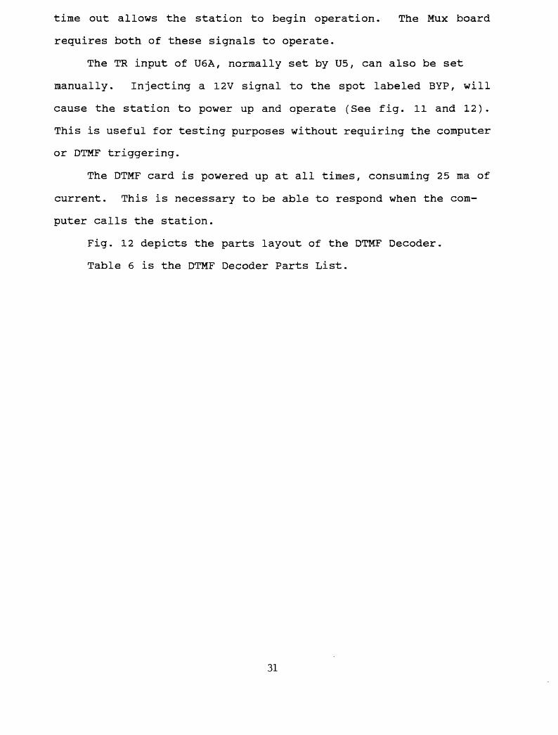
Fig. 12 depicts the parts layout of the DTMF Decoder.
Table 6 is the DTMF Decoder Parts List.
31

TI
G _1 ro
DTMF
DECODER
1
SSI2
01
Cl a TjJ
Ul
C2Rl
4800
U2
U3
4013
SI S2
U4
C3
R2
US D D-
4314
#3
S3
R3
R4
C4
BYP
U6
4098
DTME DECODER PARTS LAYOUT
DRAU
NGP
12-7-88
DESIGNED
GP 9-83
DTMF DECODER
HVO
INTERROGATION
SYSTEM
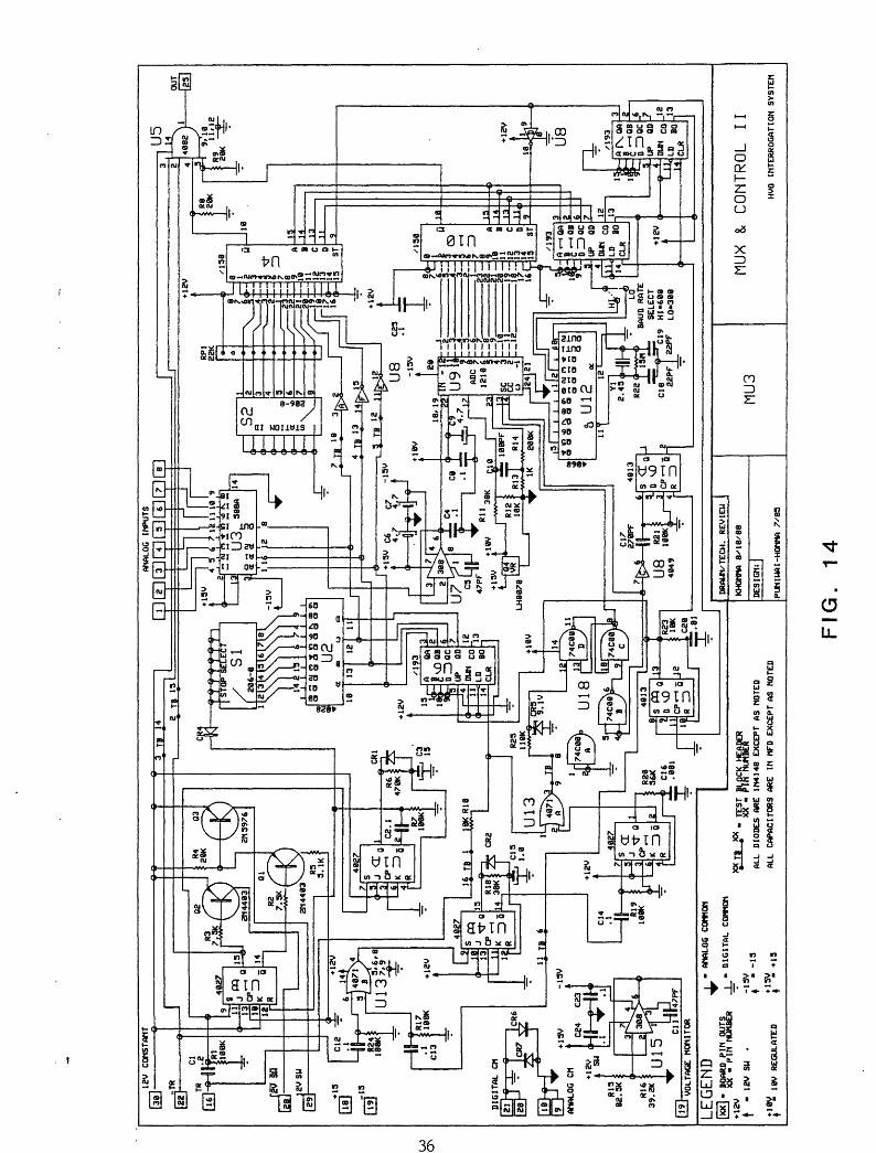
MUX & CONTROL BOARD
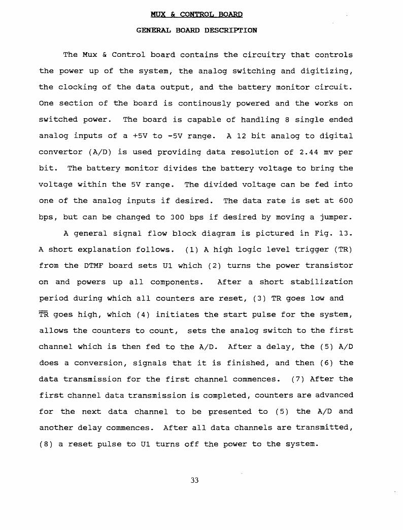
GENERAL BOARD DESCRIPTION
The Mux & Control board contains the circuitry that controls
the power up of the system, the analog switching and digitizing,
the clocking of the data output, and the battery monitor circuit.
One section of the board is continously powered and the works on
switched power. The board is capable of handling 8 single ended
analog inputs of a +5V to -5V range. A 12 bit analog to digital
converter (A/D) is used providing data resolution of 2.44 mv per
bit. The battery monitor divides the battery voltage to bring the
voltage within the 5V range. The divided voltage can be fed into
one of the analog inputs if desired. The data rate is set at 600
bps, but can be changed to 300 bps if desired by moving a jumper.
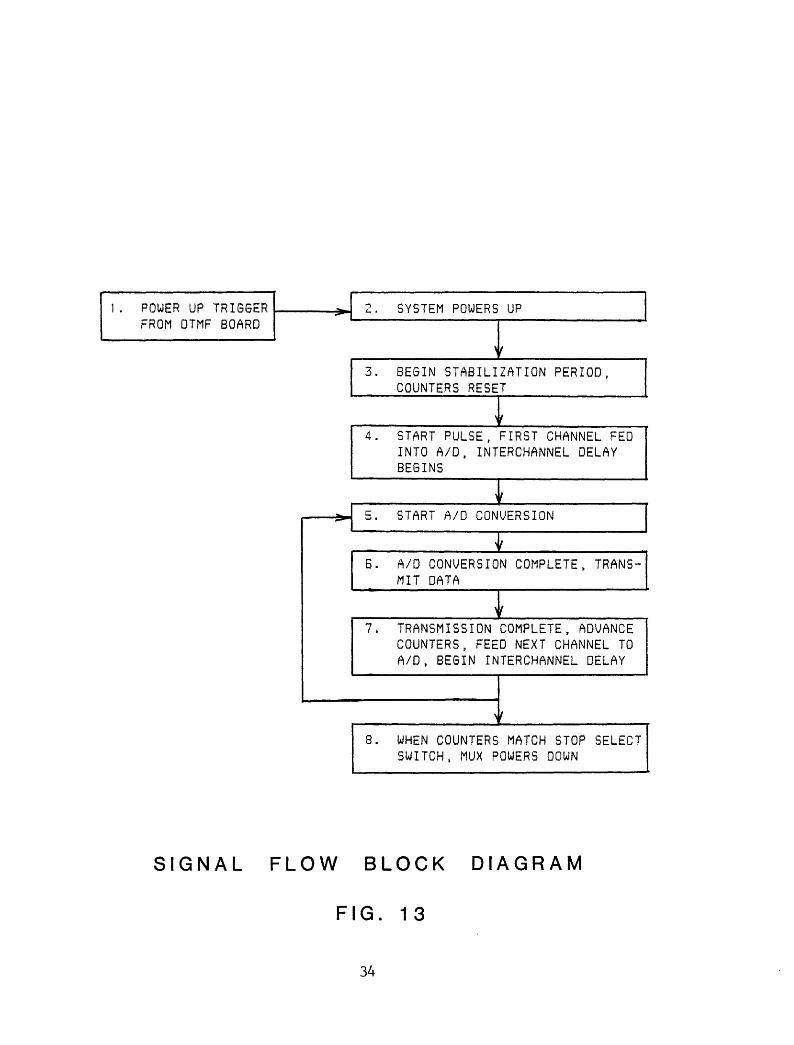
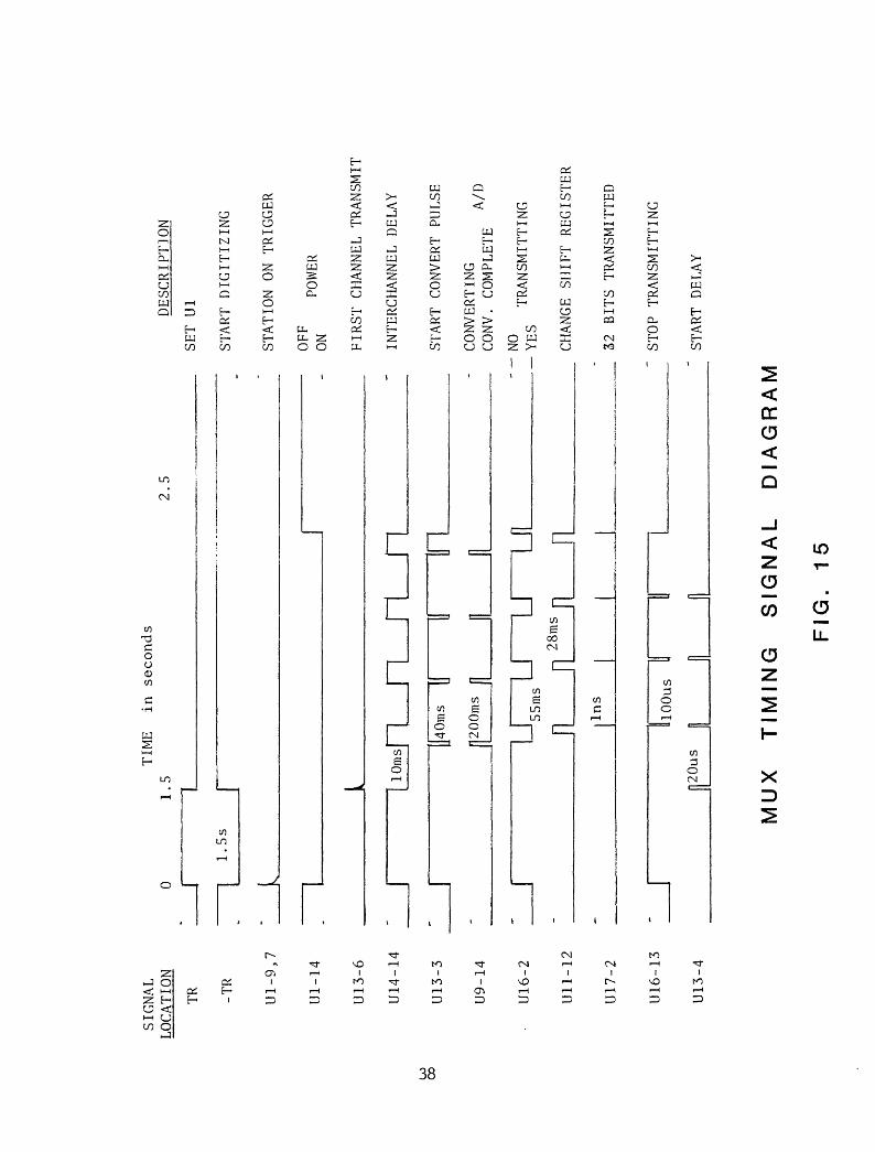
A general signal flow block diagram is pictured in Fig. 13.
A short explanation follows. (1) A high logic level trigger (TR)
from the DTMF board sets Ul which (2) turns the power transistor
on and powers up all components. After a short stabilization
period during which all counters are reset, (3) TR goes low and
TR goes high, which (4) initiates the start pulse for the system,
allows the counters to count, sets the analog switch to the first
channel which is then fed to the A/D. After a delay, the (5) A/D
does a conversion, signals that it is finished, and then (6) the
data transmission for the first channel commences. (7) After the
first channel data transmission is completed, counters are advanced
for the next data channel to be presented to (5) the A/D and
another delay commences. After all data channels are transmitted,
(8) a reset pulse to Ul turns off the power to the system.
33
1 . POWER UP TRIGGER FROM DTMF BOARD
2. SYSTEM POWERS UP
BEGIN STABILIZATION PERIOD, COUNTERS RESET
4. START PULSE, FIRST CHANNEL FED INTO A/D, INTERCHANNEL DELAY BEGINS
5. START A/D CONVERSION
B. A/D CONVERSION COMPLETE, TRANS MIT DATA
7. TRANSMISSION COMPLETE, ADVANCE COUNTERS, FEED NEXT CHANNEL TO A/D, BEGIN INTERCHANNEL DELAY
WHEN COUNTERS MATCH STOP SELECT SWITCH, MUX POWERS DOWN
SIGNAL FLOW BLOCK DIAGRAM
FIG. 13
34
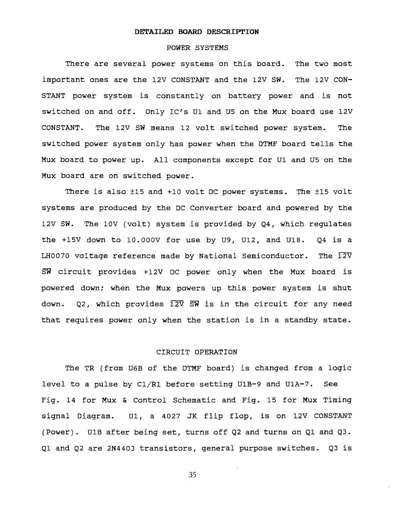
DETAILED BOARD DESCRIPTION
POWER SYSTEMS
There are several power systems on this board. The two most
important ones are the 12V CONSTANT and the 12V SW. The 12V CON
STANT power system is constantly on battery power and is not
switched on and off. Only IC's Ul and U5 on the Mux board use 12V
CONSTANT. The 12V SW means 12 volt switched power system. The
switched power system only has power when the DTMF board tells the
Mux board to power up. All components except for Ul and U5 on the
Mux board are on switched power.
There is also ±15 and +10 volt DC power systems. The ±15 volt
systems are produced by the DC Converter board and powered by the
12V SW. The 10V (volt) system is provided by Q4, which regulates
the +15V down to 10.000V for use by U9, U12, and U18. Q4 is a
LH0070 voltage reference made by National Semiconductor. The 12V
SW circuit provides +12V DC power only when the Mux board is
powered down; when the Mux powers up this power system is shut
down. Q2, which provides 12V SW is in the circuit for any need
that requires power only when the station is in a standby state.
CIRCUIT OPERATION
The TR (from U6B of the DTMF board) is changed from a logic
level to a pulse by C1/R1 before setting U1B-9 and U1A-7. See
Fig. 14 for Mux & Control Schematic and Fig. 15 for Mux Timing
signal Diagram. Ul, a 4027 JK flip flop, is on 12V CONSTANT
(Power). U1B after being set, turns off Q2 and turns on Ql and Q3.
Ql and Q2 are 2N4403 transistors, general purpose switches. Q3 is
35
12V
CONSTANT
-ft
ANALOG INPUTS
3~irr~
AN
ALO
G
CN
CI4
.1
492?
}74caev
JU
-
rg)h
^C
17
2X0P
F40
13
1 VOLTAGE MONITOR
LEGE
ND
^-HWA'Vflffii
+ 12V
|18^ 10
V REGULATED
i ANALOG COMMON
I - DIGITAL COMMON
-13V
4 -
-13
I15* +19
* n
M>
a a
a 11
&
& t_
CD a
* a
a Ul S
at a
i < >
a a
a
2 «
iT
T.4
3<
2L -1
2Z
£
°33
IHt _
R22
<1SN
L-r#
BAUD RATE
____
SELECT
C18 T C19 HI-600
22PF |
22PF
LO-300
+ 12
V
15h- A (\QA
D ZDQC
14BO
13
Tfc-
IL.*
* -
JEST BLOOOJEAgER
ALL DIODES ARE 1N4148 EXCEPT AS NOTED
ALL CAPACITORS ARE IN
MFD EXCEPT AS NOTED
KHONNA 8^18/88
DESI
GN;
|
PUNI
UAI-H
ONN
A 7/
83
MU3
MUX
CONTROL II
OUT
HVO INTERROGATION SYSTEN
FIG.
14
a 2N5976 power transistor, capable of providing 2 amps for the 12V
SW (switched power circuits). When Q3 is turned on, it provides
power to all circuitry in the electronics box (MUX, FSK, & DC
converter boards) that are not constantly powered up. Q3 is also
used to control the radio switch. The TR line is also used to:
1) reset the counter, U6, that selects the analog input to be
digitized, and 2) inhibits U13A, to prevent premature conversion
of data. The TR line is high for 1.5 seconds, at which time it
goes low and allows the U6 counter and the U13A gate to operate
normally. RIO is used to limit current sinking through U6 and U13A
from TR while these IC's are not powered and TR is high.
When TR goes low, the CLR line of U6 is released and the
outputs all go to the low state. U6 is a 74C193, a binary up/
down counter. With all the outputs low, the channel ID bus line
(the U6 outputs QA,QB,QC,QD) feeds a channel 0 ID (binary 000) to
U2, U3, and USA, F, & E. U2, a 4028 BCD to decimal decoder,
decodes the channel ID buss line into one of eight lines. The
circuitry following U2 will be covered in detail later. U3 is a
Harris HI-508A 8 channel CMOS analog multiplexer. With the U3
address lines set at channel 0, analog input 1 is switched in. The
output of U3-8, an analog voltage, is fed to U7 which buffers the
line before reaching U9. U7 and U9 will be discussed in detail
later. USA, F, & E (parts of a 4049 hex inverting buffer) invert
and feed the channel ID information to U4.
TR, also from the DTMF board, provides the first start con
version pulse to U13B and also prevents spurious data from leaving
through U5 before the system is in normal operation. U5 is a
4082 AND gate. Upon the TR transition from low to high, C12 and
37'
u> 00
SIG
NA
L
LOC
ATI
ON
TR
-TR
Ul-
9,7
Ul-
14
U13
-6
U14
-14
U13
-3
U9-
14
U16
-2
Ull
-12
U17
-2
U16
-13
U13
-4
TIME
in se
cond
s
1.5s
1.5
2.5
(J40
ms
[f
200m
s
u 55m
s
u u
i
n n2
8ms n
nIn
s
llO
Ous
20us
DESCRIPTION
SET
Ul
START DIGITIZING
STATION ON TRIGGER
OFF
ONPOWER
FIRST CHANNEL TRANSMIT
INTERCHANNEL DELAY
START CONVERT PU
LSE
CONVERTING
A/D
TRANSMITTING
CONV
. COMPLETE
NO YES
CHANGE SHIFT
REGISTER
32 BITS TRANSMITTED
STOP
TRANSMITTING
START DELAY
MU
X
TIM
ING
S
IGN
AL
D
IAG
RA
M
FIG
. 15
R24 changes the logic level to a pulse going into U13B, pin 6.
U13 is a 4071 quad OR gate. The output of U13B sets U14B, which
has a time constant set at 30ms. The 30ms time constant is de
signated as the Interchannel Delay. U14 is a 4027 dual JK flip
flop. This time constant is needed to allow the analog voltage
switched into U9 (the A/D) from U3 and U7 time to stabilize. Upon
completion of the delay, U14B-14 goes high and C14/R19 changes the
logic level into a pulse which sets U14A. U14A has a time constant
set at 56us, a pulse length determined by U9 requirements. Upon
completion of the 56us delay, the pulse from U14A passes through
U13A and on to U18. R25 and CR5 drop the 12V logic level to 10V,
to match the power levels of U18 and U9. U18 is set up as a flip-
flop to give U9 a SC (start conversion) pulse syncronized with CC
(conversion complete) to meet U9 requirements. U9 is a National
Semiconductor ADC1210, a 12-bit CMOS analog to digital converter.
U9 converts the analog voltage at its input into a 12 bit digital
signal at its output, pins 1 thru 12. When U9 has completed the
digitization, it signals by taking pin 14, the CC (conversion
complete), high. The CC is inverted by U8C, then converted by
C17/R21 into a pulse which sets U16A. U16 is a 4013 dual D flip
flop. With U16A-2 low, counters Ull and U17 commence counting and
clock out 32 pulses. Ull and U17 are 74C193 binary counters. Ull
first provides U4 then U10 sixteen timing pulses each.
U4 and U10 are 74C150, 16 line to 1 line multiplexers. Both
U4 and U10 sample the information presented to their 32 parallel
inputs and transmit the information out in a serial train of 32
bits. The first three bits out of U4 are framing bits, the next
8 are station ID, the next 3 are channel ID, and the last two are
39
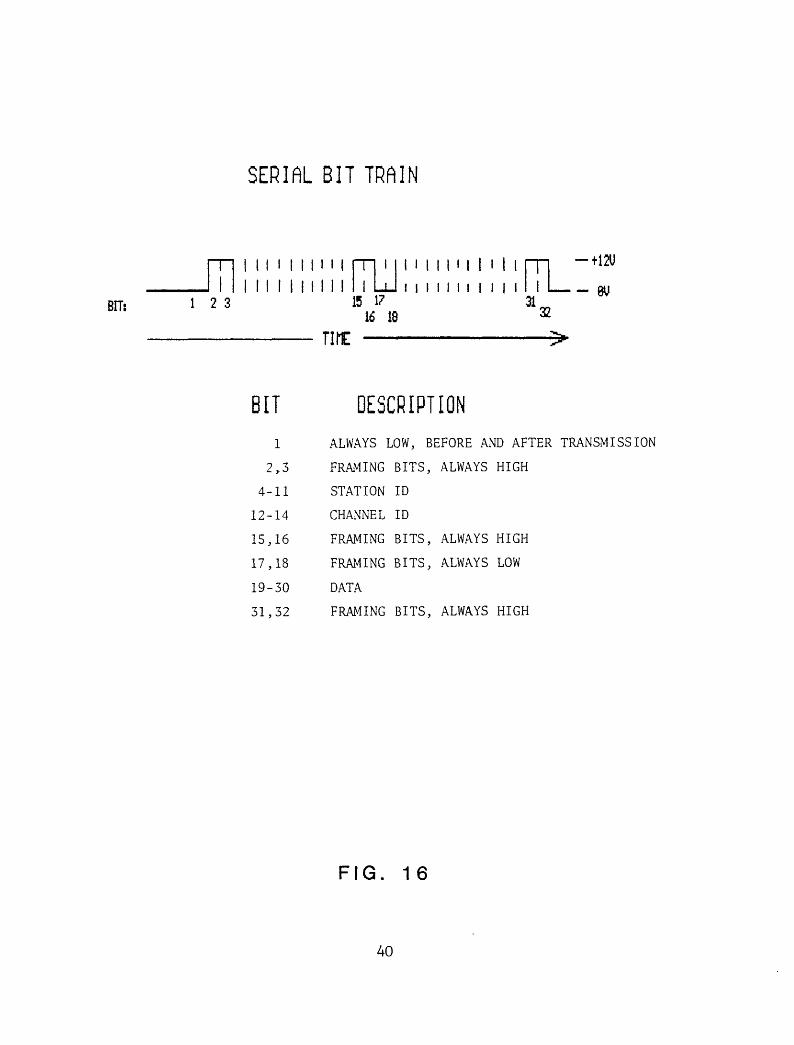
SERIAL BIT TRAIN
BIT: 1
11
2 3
II 1 1 1 1 i 1 1 1
1 1 1 1 1 I 1 1 I I
TTMT
1
I 15
16
1 1 i i i 1 i i 1 ! 1 1 i
JU i i 1 1 1 1 i 1 1 I i 17
18
1 1
31 a
2*.
- 8U
BIT1
2,3
4-11
12-14
15,16
17,18
19-30
31,32
DESCRIPTIONALWAYS LOW, BEFORE AND AFTER TRANSMISSION
FRAMING BITS, ALWAYS HIGH
STATION ID
CHANNEL ID
FRAMING BITS, ALWAYS HIGH
FRAMING BITS, ALWAYS LOW
DATA
FRAMING BITS, ALWAYS HIGH
FIG. 16
40
framing bits (fig. 16). After Ull has counted its first 16 bits,
it advances the U17 counter to one and then counts another 16
bits. U10 now transmits its 16 bits of information. U10 transmits
two framing bits, 12 bits of data, then two framing bits. The
outputs of U4-10 and U10-10 go to U5, a 4082 AND Gate. All U5
inputs must be high before a positive bit can be transmitted.
U17, during the first 16 bit transmission of U11/U4, disables U10
and allows U4 to output its data by having U17-3 low. During the
second 16 bit transmission of U11/U10, U17-3 goes high and disables
U4, allowing U10 to transmit. USD inverts the signal from U17-3,
to provide the correct signal to U10. The clocking of data by Ull
is controlled by the U12-1. U12 is a 4060 14 stage binary counter.
Jumpers labeled HI and LO are to select data transmission rate, HI
(U12-1) is 600 bps and LO (U12-2) is 300 bps- U12-5 also provides
a 76.8 Khz signal to U9. Upon completion of 32 bits, Ull-12 pulses
U17 which increments to 2. U17-2 sets U16B, which resets U16A,
which stops Ull and U17 from counting. U16B also sends a pulse to
U6 and to U13B. The pulse to U6-5 advances the counter by one,
which increments the channel bus to 1 (from 0), which causes U3 to
switch to channel two and the stop select section to channel 1.
The pulse from U16B to U13-5 sets U14B. This starts another
interchannel delay before commencing start conversion for the
second channel. The sequence of pulses will then occur as outlined
previously, for the amount of channels to be transmitted. U16B,
whose time constant is set at 1ms, is also used as a pulse
stretcher from U17-2. Our test equipment could never see the
output pulse of U17, so U16B is used as a guarantee that U6 and U13
will be triggered correctly and consistently.
41
U1A is also set when U1B is set by the TR pulse. U1A is
designed with a 7 second time constant. In the event that the
stations powers up and does not shut down, seven seconds after
power up U1A will force the system to shut down.
U2 and SI comprise the stop select section. U2, a 4028 BCD
to decimal converter, converts the Channel ID bus information to
one of ten outputs. Eight of those outputs are connected to SI,
the stop select switch bank with eight switches. Switch SI is set
for the number of channels to transmit. If, for example, we want
four channels to be transmitted, Sl-4 is set to on. After four
channels have been transmitted and counter U6 is advanced to
channel 5, a high pulse from U2-15 (signifying channel 5 on the
channel bus) passes through Sl-4 through CR4 and resets U1B-12.
This causes the MUX to power down and prevent a fifth channel from
transmitting. If SI is not set, the station will continue to
transmit until U1A forces the system to shut down.
S2 and RP1 comprise the station id section. The S2 switch
settings must match the DTMF Decoder board settings and the soft
ware settings on the central computer, otherwise the computer will
reject the data. The S2 switch must be set in binary fashion, not
decimal like the DTMF board and the computer. RP1 (22K ohm
resistor package) pulls the open switches high so there is no
floating of the inputs to U4.
U7 and U15 are LM308 operational amplifiers. U7 is used to
buffer the analog voltage between U3-8 and U9-18. U15 is used to
buffer and divide the battery voltage (12V SW) so that it can be
accepted by the analog input 1C U3. R15 and R16 form a voltage
divider on the switched power circuit, dividing the battery voltage
42
by 3.1 to be just under the +5V limit. Connecting the Battery
Monitor output to one of the input channels provides a useful
remote system check on battery status.
CR6 and CR7 are installed across the digital and analog common
to prevent voltage buildup in either common circuit.
The points labeled TB on the schematic are located on the
test block. Important signal lines are brought through the test
block for easier troubleshooting. Test block pin numbers are
noted.
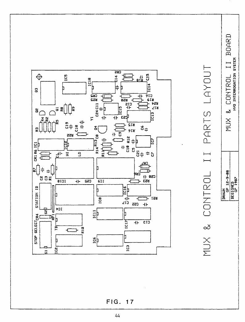
Fig. 17 is the Mux & Control Parts layout.
Table 7 is the Mux & Control Parts List.
43
T|
O
STOP SELECTCR4
STATION ID
r
NUX
CONTROL
II PARTS LAYOUT
DRAUH GP 18-9-88
DESIGNED
GP 1987
MUX
8, CONTROL
II BOARD
HVO INTERROGATION SYSTEM
VCO BOARD
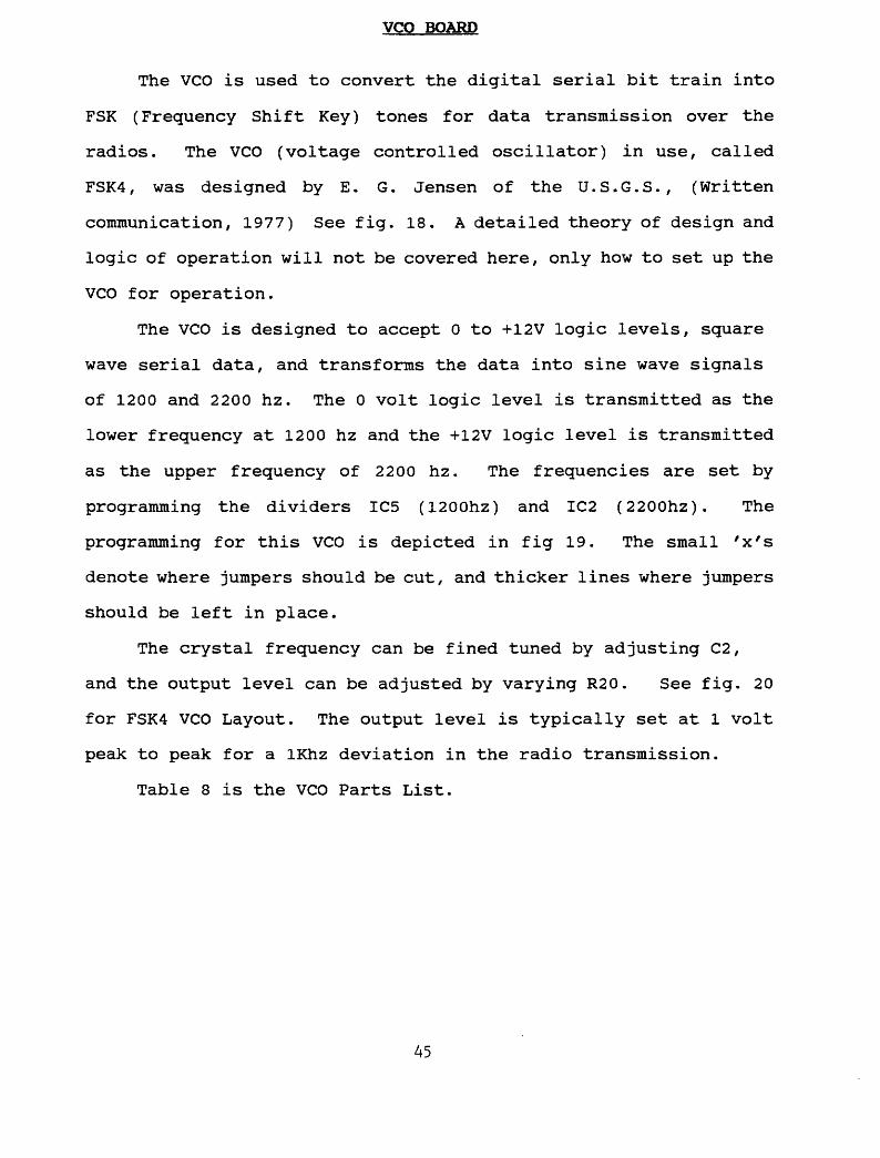
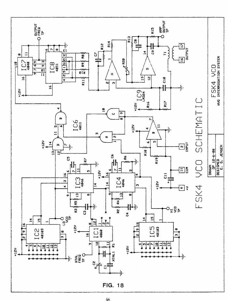
The VCO is used to convert the digital serial bit train into
FSK (Frequency Shift Key) tones for data transmission over the
radios. The VCO (voltage controlled oscillator) in use, called
FSK4, was designed by E. G. Jensen of the U.S.G.S., (Written
communication, 1977) See fig. 18. A detailed theory of design and
logic of operation will not be covered here, only how to set up the
VCO for operation.
The VCO is designed to accept 0 to +12V logic levels, square
wave serial data, and transforms the data into sine wave signals
of 1200 and 2200 hz. The 0 volt logic level is transmitted as the
lower frequency at 1200 hz and the +12V logic level is transmitted
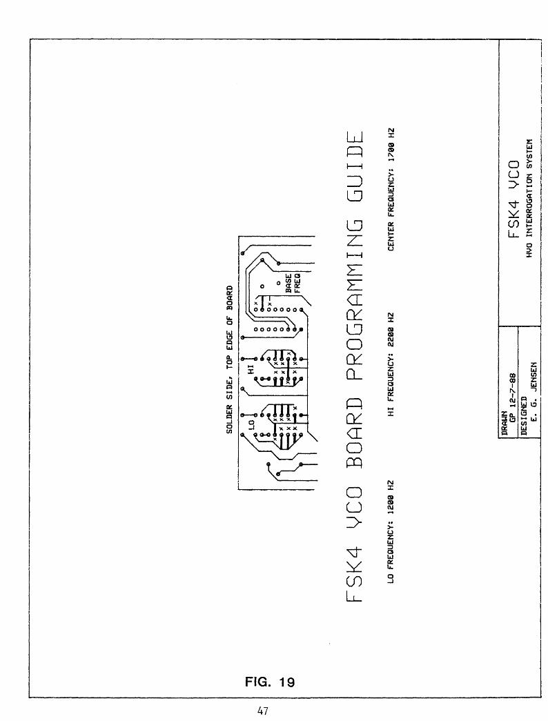
as the upper frequency of 2200 hz. The frequencies are set by
programming the dividers IC5 (1200hz) and IC2 (2200hz). The
programming for this VCO is depicted in fig 19. The small 'x's
denote where jumpers should be cut, and thicker lines where jumpers
should be left in place.
The crystal frequency can be fined tuned by adjusting C2,
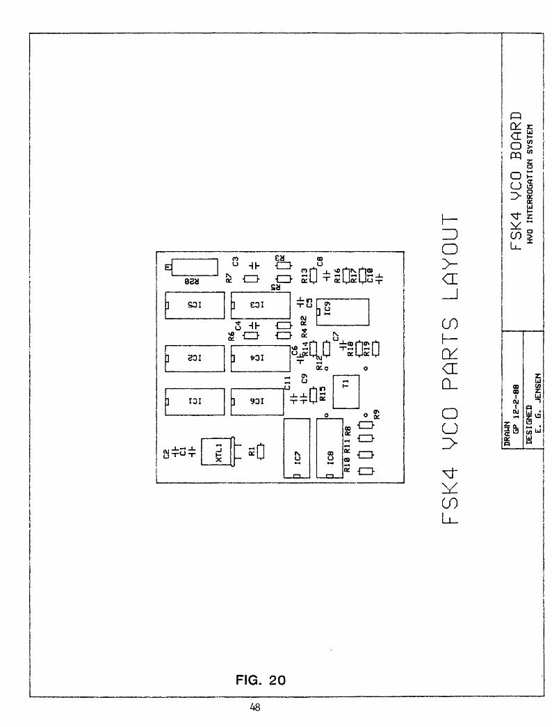
and the output level can be adjusted by varying R20. See fig. 20
for FSK4 VCO Layout. The output level is typically set at 1 volt
peak to peak for a IKhz deviation in the radio transmission.
Table 8 is the VCO Parts List.
45
+ 12
V
p _1
00
12
C5
OUTPUT
O FREQ
TP
"
IC6
4011
3 A
+ 12
Vi i
AMP
OUTPUT
COM
INPUT
OUTPUT
FSK4 YCO SCHEMATIC
DRAW
NGP
12-6-88
DESIGNED
E. G.
JENSEN
FSK4 YCO
HVO
INTERROGATION
SYSTEM
SOLD
ER SI
DE/
TOP
EDGE
OF
BOARD
3 P _A CO
FSK4 YCO BOARD PROGRAMMING GUIDE
LO FREQUENCY: 1200 HZ
HI FREQUENCY: 22
00 HZ
CENTER FR
EQUE
NCY:
1700 HZ
DRAWN
GP 12-7-88
DESI
GNED
E. G.
JENSEN
FSK4 YCO
HVO INTERROGATION SYSTEM
Tj
O ro
o
<!
ue HH Cl
Hh
XT
Ll
T~
T
Rl
CD-
!>
] IC
7
] IC
8
a i u Hh CD
0
Ri=
R18
Rll
R8
DD
DD
Cll
at
o
C9
Tl
o R9
u
R6C4
.C6
DO
CO u
C3
R4R
2
di
R18
R19
=
}
IC9
R13 ? R16
R17 -a C10
Hi
FSK4 YCO PARTS LAYOUT
DRAWN
GP 12-2-88
DESIGNED
E. G. JENSEN
FSK4 VCO BOARD
HVO INTERROGATION SYSTEM
DC CONVERTER BOARD
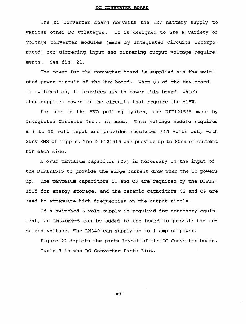
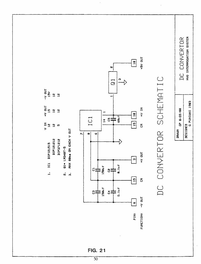
The DC Converter board converts the 12V battery supply to
various other DC volatages. It is designed to use a variety of
voltage converter modules (made by Integrated Circuits Incorpo
rated) for differing input and differing output voltage require
ments. See fig. 21.
The power for the converter board is supplied via the swit
ched power circuit of the Mux board. When Q3 of the Mux board
is switched on, it provides 12V to power this board, which
then supplies power to the circuits that require the ±15V.
For use in the HVO polling system, the DIP121515 made by
Integrated Circuits Inc., is used. This voltage module requires
a 9 to 15 volt input and provides regulated ±15 volts out, with
25mv RMS of ripple. The DIP121515 can provide up to 80ma of current
for each side.
A 68uf tantalum capacitor (C5) is necessary on the input of
the DIP121515 to provide the surge current draw when the 1C powers
up. The tantalum capacitors Cl and C3 are required by the DIP12-
1515 for energy storage, and the ceramic capacitors C2 and C4 are
used to attenuate high frequencies on the output ripple.
If a switched 5 volt supply is required for accessory equip
ment, an LM340KT-5 can be added to the board to provide the re
quired voltage. The LM340 can supply up to 1 amp of power.
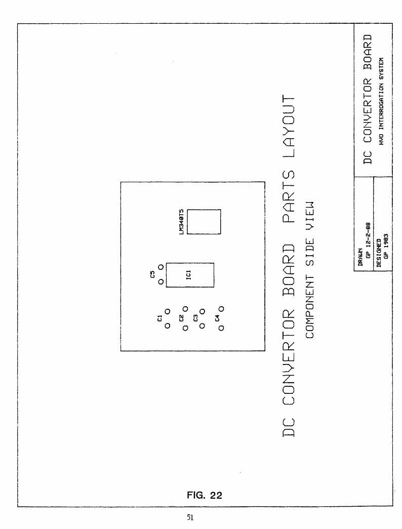
Figure 22 depicts the parts layout of the DC Converter board.
Table 8 is the DC Converter Parts List.
49
TJ
PINJ
FUNC
TION
:
1 1
V IN
+V
O
UT
-V
OU
T1.
IC
1 D
IP12
1515
12
15
15
V
DIP
1212
12
12
12
12
DIP
3712
12
5 12
12
2.
Ql-
L
M34
0T-5
3.
VIM
80
ma
ON
EA
CH
V O
UT
?
C3 II
150uf
6
i
0.<
H II
luf
V O
UT
8 T
P 1
I t
1 L
1C
l M6
-
-
-
-
I50
uf
L»C
-HI
0.1
uf
14
1
Mi
n
1 e
__
,
(J |
. 1
. 68uf
i o
VX
J
^
15
3 15
10
18
CM
+V
OU
T CM
+V
IN
+5
V
OL
DC CONYERTOR SCHEMATIC
DRAW
GP 8/22/88
DESIGNED G
PUNIUAI
1983
DC CONYERTOR
HVO
INTERROGATION
SYSTEM
P ro
ro
Cl
O
O
oC2
oC
3O
O
oC4
o
cs
O
O
ici
LM
34
0T
5
DC CONYERTOR BOARD
PARTS LAYOUT
COMPONENT SIDE YI
EU!
DRAWN
GP IE-2-88
DESIGNED
GP 1983
DC CONVERTOR BOARD
HVO INTERROGATION SYSTEM

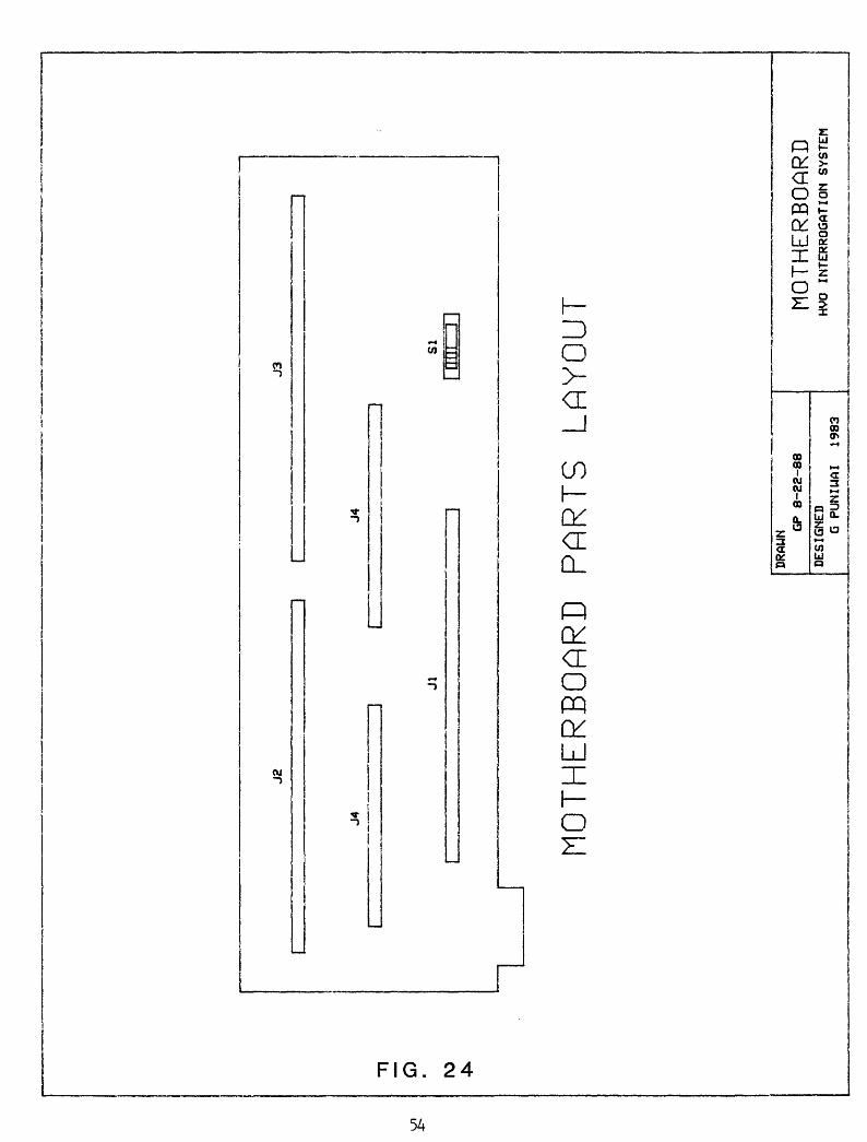
The motherboard lays in the bottom of the electronics box.
The motherboard provides the means of connecting signals and power
to the different boards and to external inputs. On it is mounted
an on off switch, card end connectors for each electronics board,
and a ribbon cable with a card end connector to connect the
motherboard to the barrier boards.
The boards that plug into the motherboard include the DTMF
Decoder, the Mux & control, the DC Converter, and the FSK board.
The DTMF, FSK, and the DC Converter all mount on 22 pin, .156"
spacing card edge connectors. The Mux & Control board mounts on
two 15 pin, .125" spacing card edge connectors. See fig. 23 for
Motherboard Schematic and fig. 24 for Motherboard Layout.
The on-off switch controls all power to the digital box and
radio box from the batteries.
52

MOTHERBOARD
CONN
.BATT
DGCM
DTMF
FSK
SER
12SU
12SU
+5V
+ 15V
-15V
VMON
ANAS
ANA?
ANA6
ANA5
ANA4
ANA3
ANA2
ANA1
CM
ON-OFF
SUITCH
hUX
BOARD
CONN.
BOARD
CONN.
MCO
BOARD
CONN
.1 2 3 4 5 6 7 R 9 10 11 12 13 14 15 16 17 18 19 20
/
BATT
° °
DGCM
SER
12SU
12SU
+ 15V
~15V
VMON
ANA8
ANA?
ANA6
ANAS
ANA4
ANA3
ANA2
ANA1
CM TR TR
30 20 25 28 29 18 TK«
19 8 7 6 5 4 3 2 1 9 16 22
21
DGCM
DTMF
12SU
18IK
4 T* 2 16 18
20
DGCM
FSK
SER
12SU
TR
12 6 21°
l?n
DGCM
7
12SU
45V
«-15V
-15V
15 10 1fl°
3 6°
DC COhVERTOR
BOARD
CONN.
MOTHERBOARD SCHEMATIC
DRAUN
DESIGNED G
PUNIWAI
1983
HVO
INTERROGATION
SYSTEM
nn
Q K)
~L
J2
J3
J4
J4
JlSI
MOTHERBOARD PARTS LAYOUT
DRAU
ING
P 8-2
2-8
8
DE
SIG
NE
DG
PUIS
IUA
I 19
83
MOTHERBOARD
HVO INTERROGATION SYSTEM
FTTTT.n RADIO SYSTEM
RADIO CONTAINER
The radios (or transceiver) are mounted in a environmental
container. The currently favored container is 4" diameter PVC pipe
fitted with end caps. Bulkhead connectors for power/signal and
antennas are mounted on one of the caps. See fig. 25 for Radio
Container Diagram. The two types of radios that are currently used
are Condel mo. TRS-20A and Monitron mo. TR-15.
The PVC or ABS type pipes are cut to 8" with end caps fitted
on both ends. On one of the caps is mounted two connectors, one
for the power and signal wires and the other for the RF output.
The power and signal bulkhead connector is an MS3102A-14S-5S, and
the RF passes though a UG-58A type N panel receptacle. Both caps
are glued to the pipe with a silicone sealant to prevent corrosive
air from entering the enclosure. The sealer can be easily removed
to access the radios. The power and signal wires from the 'MS'
type bulkhead connector are terminated with a MS3106A-14S-5P
straight connector. The MS straight connector plugs onto the
radio, the bulkhead MS connector is used with a cable to connect
with the electronics box. A short jumper from the RF panel
connector is terminated with a type 'N' male to connect to the
radio. The female side of the RF panel connector uses an RF cable
with two 'N' connectors to connect to the antenna. The completed
radio container is usually mounted to a mast with two hose clamps.
See Table 11 for MS pin designations, color codes, and radio box
parts list.
55
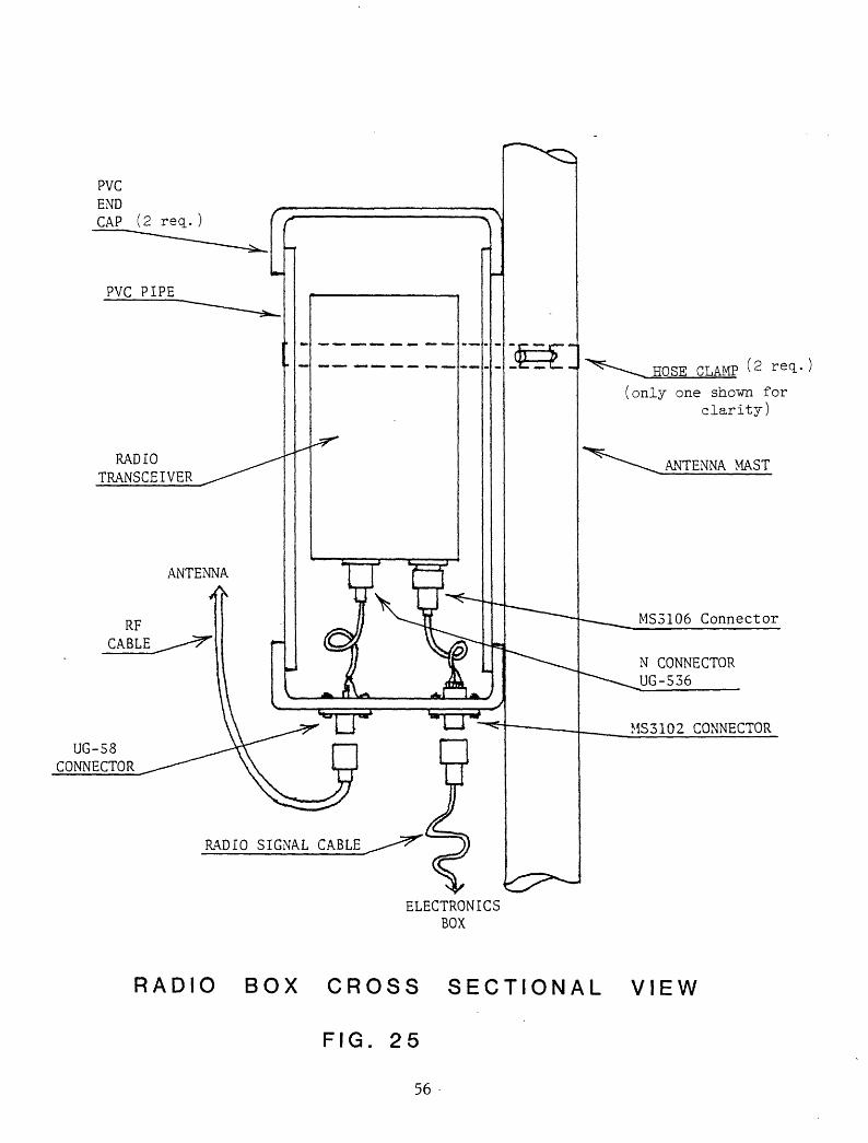
PVC END CAP (2 req.
RADIO SIGNAL CABLE
UG-58 CONNECTOR
ELECTRONICS BOX
HOSE CLAMP 2 re(l'
(only one shown for clarity)
ANTENNA MAST
MS3106 Connector
N CONNECTOR UG-556
MS3102 CONNECTOR
RADIO BOX CROSS SECTIONAL VIEW
FIG. 25
56
RADIOS
Both the Condel and Monitron radios used in the radio box are
transceivers, containing both a radio receiver and a radio
transmitter. There is a switch which transfers power and antenna
connections between the receiver and transmitter.
The only adjustments on the transceiver is a squelch and a
output level. The squelch is adjusted to the most sensitive
position before the squelch is broken, and the output level is
adjusted for 1 volt peak to peak.
Stations that have line of site with the HVO receive and
transmit on the Fl radio frequency, 171.219 Mhz. Stations that
do not have line of site with the HVO operate with the repeater
on Mauna Kea. The stations using the repeater transmit on 166.4187
Mhz and receive on 171.219 Mhz.
ANTENNAS
Most sites use a gain antenna because of the low RF power
levels. A Scala CA5-150V, a vertically polarized yagi antenna with
9 db, is the antenna used for remote stations. Stations within 5
miles of the observatory utilize a simple whip antenna for radio
communication.
57
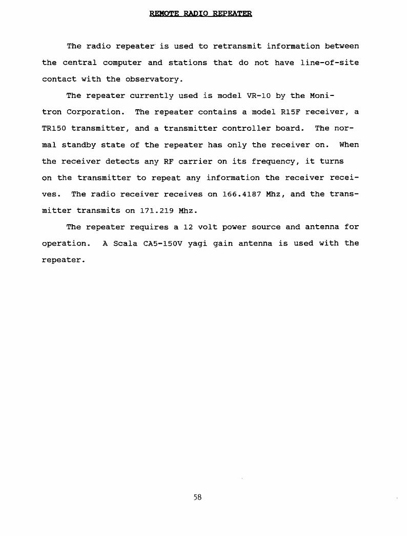
REMOTE RADIO REPEATER
The radio repeater is used to retransmit information between
the central computer and stations that do not have line-of-site
contact with the observatory.
The repeater currently used is model VR-10 by the Moni-
tron Corporation. The repeater contains a model R15F receiver, a
TR150 transmitter, and a transmitter controller board. The nor
mal standby state of the repeater has only the receiver on. When
the receiver detects any RF carrier on its frequency, it turns
on the transmitter to repeat any information the receiver recei
ves. The radio receiver receives on 166.4187 Mhz, and the trans
mitter transmits on 171.219 Mhz.
The repeater requires a 12 volt power source and antenna for
operation. A Scala CA5-150V yagi gain antenna is used with the
repeater.
58

OPERATION
This section provides instructions to operate a field unit
and have it acccessed by the control computer.
The first job to be done in setting up a station is to pro
gram the host computer with the station information. This in
cludes the station name, station id number, transmitter freq-
quency number, polling period, subnet id, number of channels,
Mux serial number, zero volt bit count, battery conversion fac
tor, and battery status flag. Refer to OFR 87-633.
The next job entails programming the digital box and re
quires setting switches on the Mux & Control and DTMF board.
The three dipswitches on the DTMF board will be set first.
The switches must be set in sequential order (first SI, then S2 and
finally S3) to match the station id number that was programmed into
the computer. If, for example, the station id number on the
computer is 025, then set switch #1 on the DTMF board to 0, switch
#2 to 2, and switch #3 to 5. The DTMF board will now send the
appropiate signals to activate the Mux card only after the computer
transmits the DTMF code " 0 2 5".
The next task is to set the Station Id switch (S2) on the Mux
card. This switch is programmed in binary code. The eight
positions on the dipswitch allow 256 units, which limits this
system to 256 stations. So, the decimal number 025 (from the
example) must be converted to a binary number, which is 10011000
in binary base 2. Set dipswitch S2 position 1 (S2-1) to On, S2-2
to off, S3-3 to off, S2-4 to on, S2-5 to on, and S2-6, 7, and 8 to
off. S2-1 is binary 2 7 and S2-8 is binary 2°. The information from
59
S2 is transmitted with each channel of data, which the host
computer will then verify before accepting the data. This check
will also insure that the data that is received is from the same
station that the computer called.
The last switch to set is SI on the Mux card, the Stop Se
lect. Simply count how many channels of information is to be
sent and set that number on the switch to on. The rest of the
switches must be set to off. Example; if four channels of data
are to be sent, set Sl-4 to on and all other switches to off.
The number of channels set should coincide with the computer
program, if it is less than the computer expects it will repeat
edly try to gather data. If it is more than computer is pro
grammed for, the computer will ignore the excess channels.
60

REFERENCES CITED
1. Roger, J. , Johnston, M. J. S. , Mortensen, C., and Myren, G. ,
1977, A Multi-channel Digital Telemetry System for Low
Frequency Geophysical Data: U.S. Geological Survey Open-File
Report 77-490, p. 111.
2. English, T. T. , 1987, HVO Polling Telemetry System for Low
Frequency Data Acquisition: Software Users' Guide: U. S.
Geological Survey Open-File Report 87-633, 51 p.
61

APPLE INTERFACE PARTS LIST
DESG DESCRIPTION
Ul CD4049BE Invertor 1U2 6522 Versastile Interface Adaptor 1U3 S2559A Tone Generator 1U4 XR2211 FSK Demodulator 1
Rl IK, 1/4W, 5% Resistor 1R2, 3 4.7K Resistor 2R4 1.3K Resistor 1R5 10M Resistor 1R6 51K Resistor 1R7 20K Resistor 1R8 100K Resistor 1R9 510K Resistor 1RIO 5.IK Resistor 1Rll, 12 5K, 20 turn, 3/4" rectangular 2
Potentiometer
Cl lOpf Ceramic Capacitor 1C2 0.002[if Ceramic Capacitor 1C3 0.022[if Ceramic Capacitor 1C4, 6, 8 O.lfif Ceramic Capacitor 3C5 0.0047iif Ceramic Capacitor 1C7 0. 5[if Ceramic Capacitor 1
Yl 3.58 Mhz Crystal 1
Tl 42LH016 Mouser Transformer 1
Dl thru D7 1N914 Diode 7
Jl 14 DIP Header w/ribbon cable 114 DIP Socket 2 16 DIP Socket 2 40 DIP Socket 1
TABLE 1
62
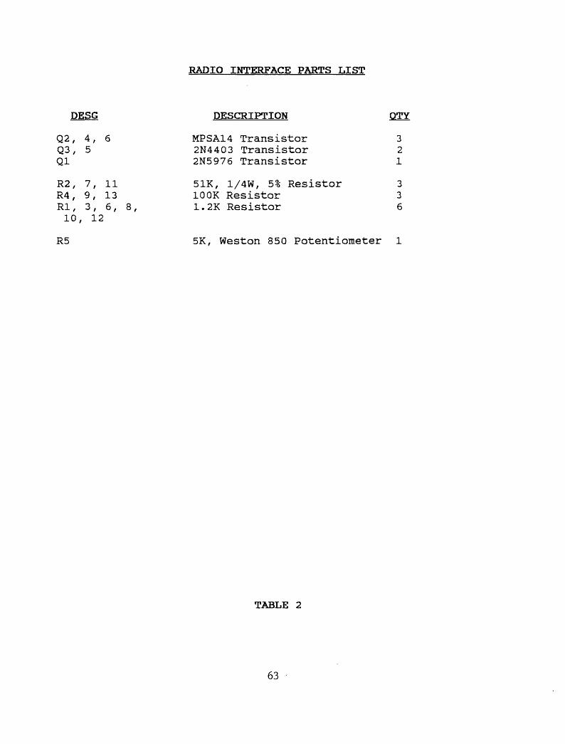
RADIO INTERFACE PARTS LIST
DESG DESCRIPTION QTY
Q2, 4, 6 MPSA14 Transistor 3Q3, 5 2N4403 Transistor 2Ql 2N5976 Transistor 1
R2, 7, 11 51K, 1/4W, 5% Resistor 3R4, 9, 13 100K Resistor 3Rl, 3, 6, 8, 1.2K Resistor 6 10, 12
R5 5K, Weston 850 Potentiometer 1
TABLE 2
63
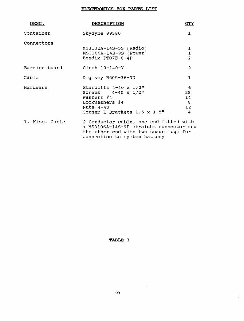
ELECTRONICS BOX PARTS LIST
DESG. DESCRIPTION QTY
Container Skydyne 99380 1
ConnectorsMS3102A-14S-5S (Radio) 1 MS3106A-14S-9S (Power) 1 Bendix PT07E-8-4P 2
Barrier board Cinch 10-140-Y 2
Cable Digikey R505-36-ND 1
Hardware Standoffs 4-40 x 1/2" 6Screws 4-40 x 1/2" 28Washers #4 14Lockwashers #4 8Nuts 4-40 12Corner L Brackets 1.5 x 1.5" 4
1. Misc. Cable 2 Conductor cable, one end fitted witha MS3106A-14S-9P straight connector and the other end with two spade lugs for connection to system battery
TABLE 3
64
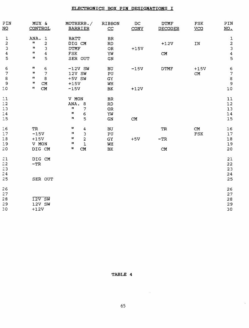
ELECTRONICS BOX PIN DESIGNATIONS I
MUX & CONTROL
MOTHERS./ BARRIER
RIBBON CC
12345
6789
10
1112131415
1617181920
2122
ANA. 1" 211 3« 411 5
" 6it 7
" 8" CM11 CM
TR-15V+15VV MONDIG CM
DIG CM-TR
BATTDIG CMDTMFFSKSER OUT
-12V SW12V SW+5V SW+15V-15V
V MONANA. 8
it 7
" 611 5
« 411 3
" 2ii x11 CM
BRRDORYWGN
BUPUGYWHBK
BRRDORYWGN
BUPUGYWHBK
232425 SER OUT
12V SW 12V SW +12V
DC CONV
+15V
-15V
+12V
DTMF DECODER
+12V
CM
DTMF
FSK VCO
IN
+15V CM
CM
+5V
TR
-TR
CM
CM FSK
PIN NO.
12345
6789
10
1112131415
1617181920
2122232425
2627282930
TABLE 4
65
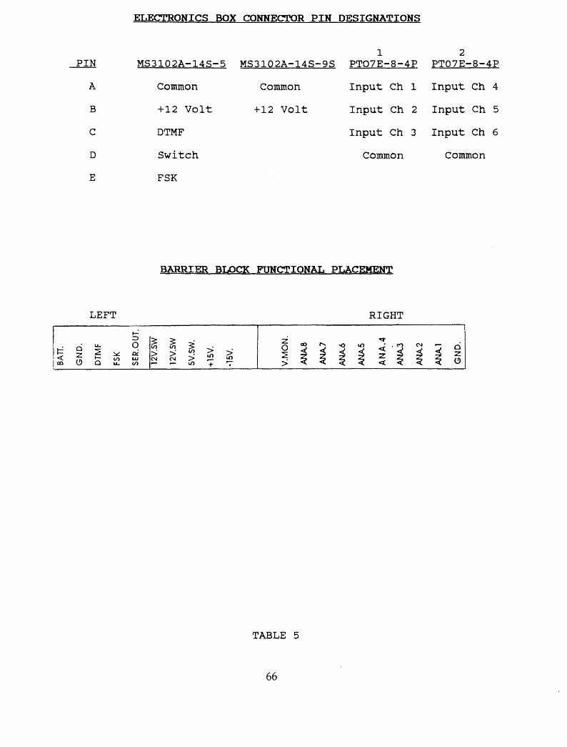
ELECTRONICS BOX CONNECTOR PIN DESIGNATIONS
PIN1 2
MS3102A-14S-5 MS31Q2A-14S-9S PTO7E-8-4P PT07E-8-4P
A
B
C
D
E
Common
+12 Volt
DTMF
Switch
FSK
Common Input
+12 Volt Input
Input
Ch 1
Ch 2
Ch 3
Common
Input Ch 4
Input Ch 5
Input Ch 6
Common
BARRIER BLOCK FUNCTIONAL PLACEMENT
LEFT RIGHT
1= S< zm O
oQ u. co
CO tO2 O
a < '
TABLE 5
66

DTMF DECODER PARTS LIST
TABLE 6
DESG. DESCRIPTION
Ul SSI201 DTMF Decoder 1U2 4000 Invertor 1U3 4514 4 to 16 Line Decoder 1U4,5 4013 D Flip-Flop 2U6 4098 Multivibrator 1
Rl 10M, 1/4W, 5% Resistor 1R2 100K Resistor 1R3 1.5M Resistor 1R4 4.7M Resistor 1
Cl, 2, 3 O.Oluf Ceramic Capacitor 3C4 3.3uf Tantalum Capacitor 1C5 1.5uf Tantalum Capacitor 1
Yl 3.579 Mhz Crystal 1
SI, 2, 3 76SB10 Grayhill Dipswitch 3
14 DIP Socket 316 DIP Socket 122 DIP Socket 124 DIP Socket 1
67
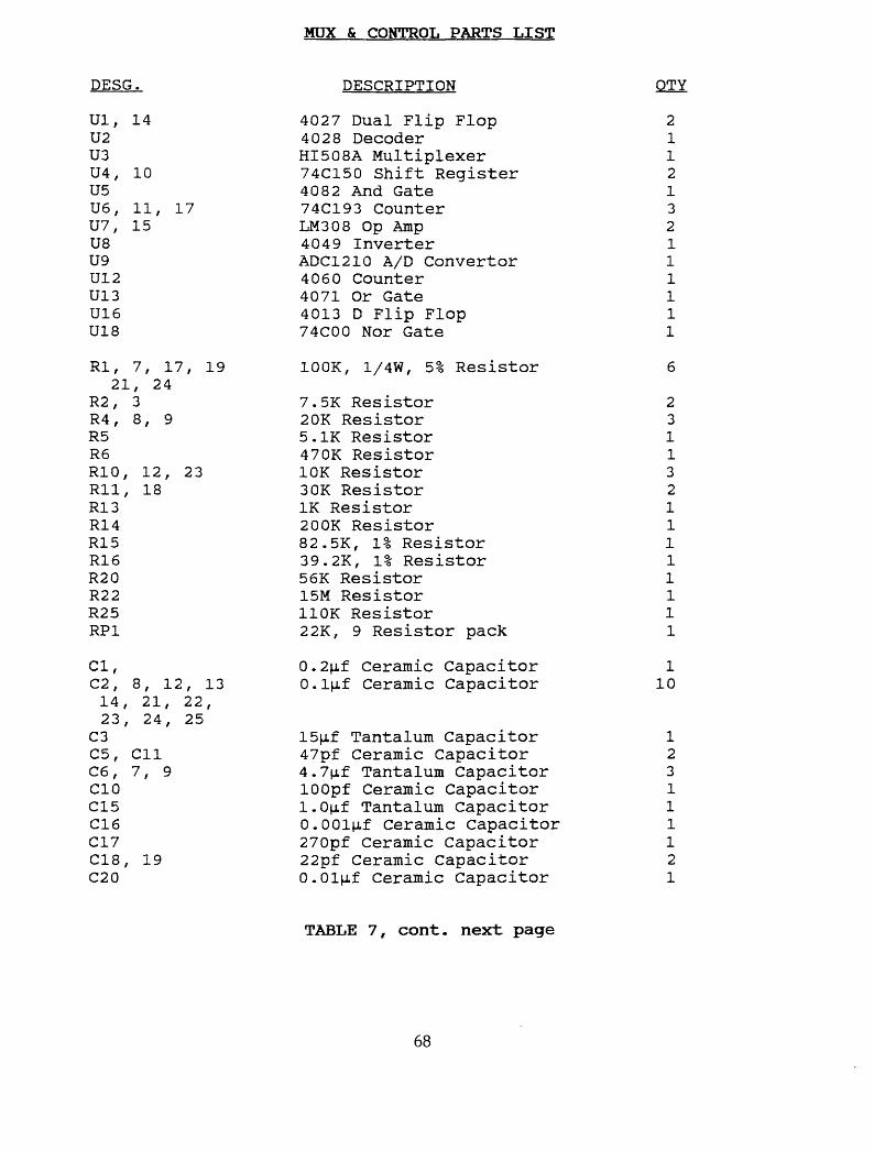
MOX & CONTROL PARTS LIST
DESG. DESCRIPTION QTY
Ul, 14 4027 Dual Flip Flop 2U2 4028 Decoder 1U3 HI508A Multiplexer 1U4, 10 74C150 Shift Register 2U5 4082 And Gate 1U6, 11, 17 74C193 Counter 3137 1 15 LM308 Op Amp 2U8 4049 Inverter 1U9 ADC1210 A/D Converter 1U12 4060 Counter 1U13 4071 Or Gate 1U16 4013 D Flip Flop 1U18 74COO Nor Gate 1
Rl, 7, 17, 19 100K, 1/4W, 5% Resistor 621, 24
R2, 3 7.5K Resistor 2R4, 8, 9 20K Resistor 3R5 5.IK Resistor 1R6 470K Resistor 1RIO, 12, 23 10K Resistor 3Rll, 18 30K Resistor 2R13 IK Resistor 1R14 200K Resistor 1R15 82.5K, 1% Resistor 1R16 39.2K, 1% Resistor 1R20 56K Resistor 1R22 15M Resistor 1R25 110K Resistor 1RP1 22K, 9 Resistor pack 1
Cl, 0.2|if Ceramic Capacitor 1C2, 8, 12, 13 O.lM-f Ceramic Capacitor 1014, 21, 22,23, 24, 25
C3 15M-f Tantalum Capacitor 1C5, Cll 47pf Ceramic Capacitor 2C6, 7, 9 4.7M-f Tantalum Capacitor 3CIO lOOpf Ceramic Capacitor 1C15 1.0|if Tantalum Capacitor 1C16 O.OOljif Ceramic Capacitor 1C17 270pf Ceramic Capacitor 1CIS, 19 22pf Ceramic Capacitor 2C20 O.Ol^if Ceramic Capacitor 1
TABLE 7, cont. next page
68

TABLE 7, cont
MUX & CONTROL PARTS LIST cont.
DESG. DESCRIPTION
CR1, 2, 4, 6, 7 1N4148 Diode 5 CR5 9.1V Zener Diode 1
Ql, Q2 2N4403 Transistor 2Q3 2N5976 Transistor 1Q4 LH0070-1H Voltage Regulator 1
Yl 2.4576 Mhz Crystal 1
SI, S2 206-8 CTS Dipswitch 2
TB1 16 DIP Header 1
8 DIP Socket 214 DIP Socket 416 DIP Socket 924 DIP Socket 3
There is no CR3 and no C4.
69
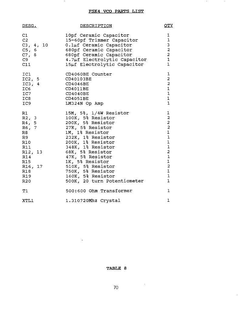
FSK4 VCO PARTS LIST
DESG. DESCRIPTION
Cl lOpf Ceramic Capacitor 1C2 15-60pf Trimmer Capacitor 1C3, 4, 10 O.lp,f Ceramic Capacitor 3C5, 6 680pf Ceramic Capacitor 2C7, 8 680pf Ceramic Capacitor 2C9 4.7p.f Electrolytic Capacitor 1Cll 15nf Electrolytic Capacitor 1
IC1 CD4060BE Counter 1IC2, 5 CD40103BE 2IC3, 4 CD4046BE 2IC6 CD4011BE 1IC7 CD4040BE 1IC8 CD4051BE 1IC9 LM324N Op Amp 1
Rl 15M, 5%, 1/4W Resistor 1R2, 3 100K, 5% Resistor 2R4, 5 200K, 5% Resistor 2R6, 7 27K, 5% Resistor 2R8 1M, 1% Resistor 1R9 232K, 1% Resistor 1RIO 200K, 1% Resistor 1Rll 348K, 1% Resistor 1R12, 13 68K, 5% Resistor 2R14 47K, 5% Resistor 1R15 IK, 5% Resistor 1R16, 17 510K, 5% Resistor 2R18 750K, 5% Resistor 1R19 160K, 5% Resistor 1R20 500K, 20 turn Potentiometer 1
Tl 500:600 Ohm Transformer 1
XTL1 1.310720Mhz Crystal 1
TABLE 8
70
DC CONVERTER PARTS LIST
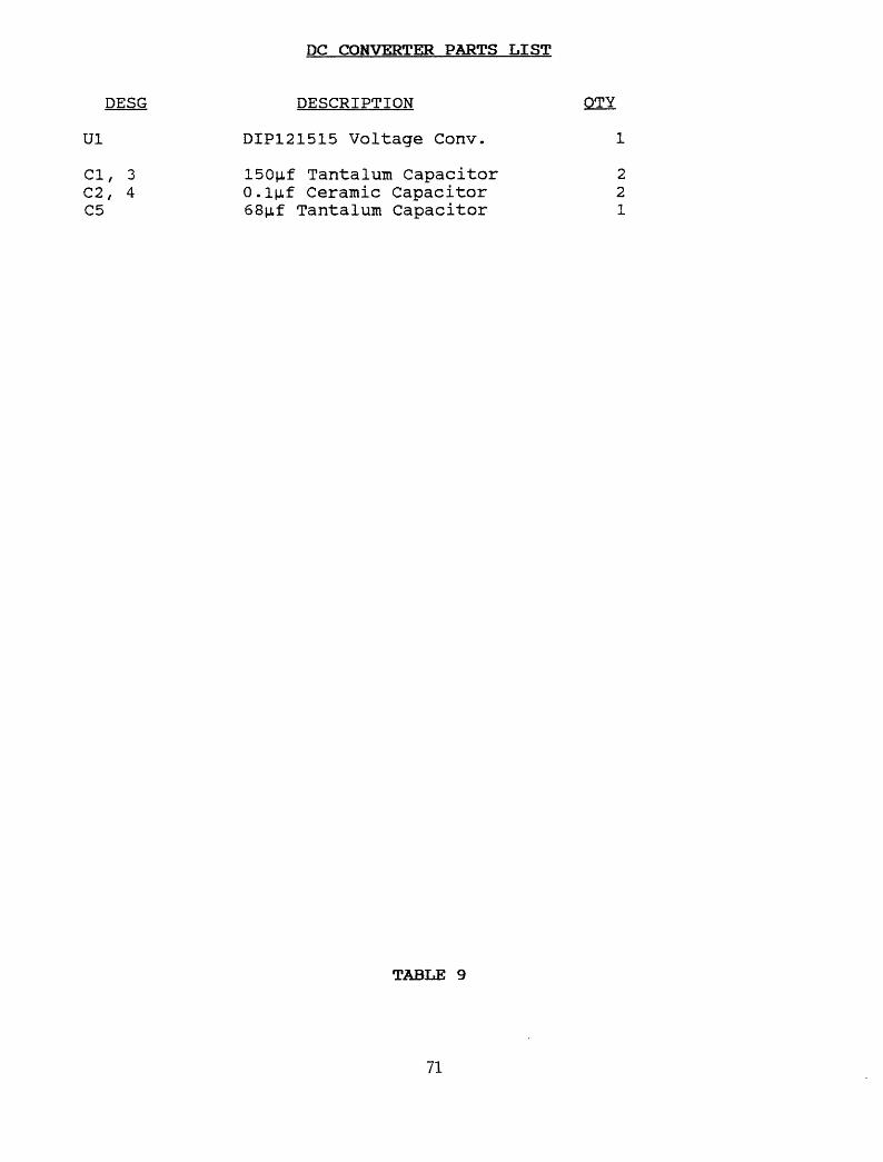
DESG DESCRIPTION OTY
Ul DIP121515 Voltage Conv. 1
Cl, 3 150fj.f Tantalum Capacitor 2C2, 4 O.ljif Ceramic Capacitor 2C5 68p,f Tantalum Capacitor 1
TABLE 9
71
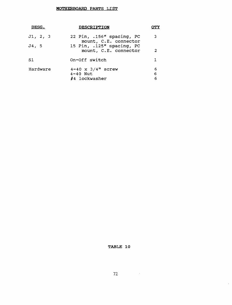
MOTHERBOARD PARTS LIST
DESG. DESCRIPTION
Jl, 2, 3 22 Pin, .156" spacing, PC 3mount , C. E. connector
J4, 5 15 Pin, .125" spacing, PCmount, C.E. connector 2
SI On-Off switch 1
Hardware 4-40 x 3/4" screw 64-40 Nut 6#4 lockwasher 6
TABLE 10
72
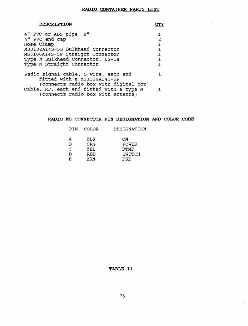
RADIO CONTAINER PARTS LIST
DESCRIPTION
4" PVC or ABS pipe, 8" 14" PVC end cap 2Hose Clamp 1MS3102A14S-5S Bulkhead Connector 1MS3106A14S-5P Straight Connector 1Type N Bulkhead Connector, UG-58 1Type N Straight Connector 1
Radio signal cable, 5 wire, each end 1 fitted with a MS3106A14S-5P (connects radio box with digital box)
Cable, RF, each end fitted with a type N 1 (connects radio box with antenna)
RADIO MS CONNECTOR PIN DESIGNATION AND COLOR CODE
PIN COLOR DESIGNATION
A BLK CMB ORG POWERC YEL DTMFD RED SWITCHE BRN FSK
TABLE 11
73
Recommended