Future Technology Devices International Ltd (FTDI)
Unit 1, 2 Seaward Place, Centurion Business Park, Glasgow, G41 1HH, United Kingdom
Tel.: +44 (0) 141 429 2777 Fax: + 44 (0) 141 429 2758
E-Mail (Support): [email protected]
Web: http://www.vinculum.com
Neither the whole nor any part of the information contained in, or the product described in this manual, may be adapted or reproduced
in any material or electronic form without the prior written consent of the copyright holder. This product and its documentation are supplied on an as-is basis and no warranty as to their suitability for any particular purpose is either made or implied. Future Technology
Devices International Ltd will not accept any claim for damages howsoever arising as a result of use or failure of this product. Your
statutory rights are not affected. This product or any variant of it is not intended for use in any medical appliance, device or system in
which the failure of the product might reasonably be expected to result in personal injury. This document provides preliminary
information that may be subject to change without notice. No freedom to use patents or other intellectual property rights is implied by
the publication of this document. Future Technology Devices International Ltd, Unit 1, 2 Seaward Place, Centurion Business Park,
Glasgow, G41 1HH, United Kingdom. Scotland Registered Number: SC136640
Copyright © 2010 Future Technology Devices International Limited
Future Technology Devices International Ltd.
V2DIP1-48
VNC2-48 Development Module
Datasheet
Document Reference No.: FT_000236
Version 1.01
Issue Date: 2010-05-24

`
Copyright © 2010 Future Technology Devices International Limited 1
Document Reference No.: FT_000236 V2DIP1-48 VNC2-48 Development Module Datasheet Version 1.01
Clearance No.: FTDI# 153
1 Introduction
V2DIP1-48 module is designed to allow rapid development of designs using the VNC2-48Q IC. The V2DIP1-48 is supplied as a PCB designed to fit into a 24 pin 0.6” wide 0.1” pitch DIP socket.The module provides access to the UART, parallel FIFO, and SPI interface pins of the VNC2-48Q device, via onboard header pins. The module has a single USB ports which is accessible via the onboard type A USB
connector.
Figure 1.1- V2DIP1 48
The VNC2 is the second of FTDI’s Vinculum family of Embedded dual USB host controller devices. The VNC2 device provides USB Host interfacing capability for a variety of different USB device classes including support for BOMS (bulk only mass storage), Printer, HID (human interface devices). For mass storage devices such as USB Flash drives, VNC2 also transparently handles the FAT file structure.
Communication with non USB devices such as a low cost microcontroller is accomplished via either UART, SPI or parallel FIFO interfaces. The VNC2 provides a new cost effective solution for providing USB Host
capability into products that previously did not have the hardware resources available.
The VNC2 supports the capability to enable customers to develop custom firmware using the Vinculum II development software tool suite. The development tools support compiler, linker and debugger tools complete within an integrated development environment (IDE).
The Vinculum-II VNC2 family of devices are available in Pb-free (RoHS compliant) 32-lead LQFP, 32-lead QFN, 48-lead LQFP, 48-lead QFN, 64-Lead lQFP and 64-lead QFN packages.

`
Copyright © 2010 Future Technology Devices International Limited 2
Document Reference No.: FT_000236 V2DIP1-48 VNC2-48 Development Module Datasheet Version 1.01
Clearance No.: FTDI# 153
Table of Contents
1 Introduction............................................................................................ 1
2 Features ................................................................................................. 3
3 Pin Out and Signal Description ............................................................ 4
3.1 Module Pin Out .................................................................................................... 4
3.2 Pin Signal Description ........................................................................................ 6
3.3 I/O Configuration Using The Jumper Pin Header ............................................. 8
3.4 Default Interface I/O Pin Configuration .............................................................. 9
3.5 UART Interface ................................................................................................... 10
3.5.1 Signal Description – UART Interface .............................................................................. 10
3.6 Serial Peripheral Interface (SPI) ....................................................................... 11
3.6.1 Signal Description - SPI Slave ........................................................................................ 11
3.6.2 Signal Description - SPI Master ...................................................................................... 11
3.7 Parallel FIFO Interface-Asynchronous Mode .................................................. 12
3.7.1 Signal Description - Parallel FIFO Interface ................................................................. 12
3.7.2 Timing Diagram – Asynchronous FIFO Mode Read and Write Cycle ..................... 13
3.8 Parallel FIFO Interface-Synchronous Mode .................................................... 14
3.8.1 Timing Diagram – Synchronous FIFO Mode Read and Write Cycle ....................... 14
3.9 Debugger Interface ............................................................................................ 16
3.9.1 Signal Description - Debugger Interface ...................................................................... 16
4 Firmware .............................................................................................. 17
4.1 Firmware Support .............................................................................................. 17
4.2 Available Firmware ............................................................................................ 17
4.3 Firmware Upgrades ........................................................................................... 17
5 External circuit Configuration ............................................................ 18
5.1 Adding a second USB Port ............................................................................... 18
6 Mechanical Dimensions ...................................................................... 19
7 Schematic Diagram ............................................................................. 20
8 Contact Information............................................................................. 21
Appendix A – References ............................................................................................ 22
Appendix B – List of Figures and Tables ................................................................... 23
List of Figures............................................................................................................... 23
List of Tables ................................................................................................................ 23
Appendix C – Revision History ................................................................................... 24

`
Copyright © 2010 Future Technology Devices International Limited 3
Document Reference No.: FT_000236 V2DIP1-48 VNC2-48 Development Module Datasheet Version 1.01
Clearance No.: FTDI# 153
2 Features
The V2DIP1 48 incorporates the following features:
Uses FTDI’s VNC2-48Q embedded USB host controller IC device
Single USB ‘A’ type socket to interface with USB peripheral devices
Connnection to a second USB interface port available via module I/O pins if required.
Jumper selectable UART, parallel FIFO or SPI MCU interfaces
UART, parallel FIFO and SPI interfaces can be programmed to a choice of available I/O pins
Single 5V supply input from DIL connectors or 5V supplied via USB VBUS slave interface or debugger module.
All VNC2 signals available on 0.6” wide, 0.1” pitch DIL male connectors.
Auxiliary 3.3 V / 200 mA power output to external logic.
Power and traffic indicator LED’s
V2DIP1-48 is a Pb-free, RoHS complaint development module.
Debugger interface pin available via 6 way male header which interfaces to separate debugger module.
Firmware upgrades via UART or debugger interface.
FOC software development supported through Vinculum software development tool suite IDe consisting integrated compiler, linker, and debugger capabilities.

`
Copyright © 2010 Future Technology Devices International Limited 4
Document Reference No.: FT_000236 V2DIP1-48 VNC2-48 Development Module Datasheet Version 1.01
Clearance No.: FTDI# 153
3 Pin Out and Signal Description
3.1 Module Pin Out
Figure 3.1 - V2DIP1 48 Module Pin Out (Top View)

`
Copyright © 2010 Future Technology Devices International Limited 5
Document Reference No.: FT_000236 V2DIP1-48 VNC2-48 Development Module Datasheet Version 1.01
Clearance No.: FTDI# 153
Figure 3.2 - V2DIP1 48 Module Pin Out (Bottom View)

`
Copyright © 2010 Future Technology Devices International Limited 6
Document Reference No.: FT_000236 V2DIP1-48 VNC2-48 Development Module Datasheet Version 1.01
Clearance No.: FTDI# 153
3.2 Pin Signal Description
Pin No.
(VDIP1)
Name
(VDIP1)
Pin
Name
on PCB
Type Description
J1-1
(1)
5V0 5V0 PWR Input 5.0V module supply pin. This pin can be used to provide the 5.0V
input to the V2DIP1-48 when the V2DIP1-48 is not powered from the
USB connector (VBUS) or the debugger interface. Also connected to
DIL connector pins J1-2, J1-3 and J1-9 and J3-6.
J1-2
(2)
IOBUS5 IO5
Output USB port 1 traffic activity indicator LED. This pin is hard wired to a green LED on boardthe PCB. It is also brought out onto this pin which allows for the possibility of bringing an additional LED traffic indicator out of the V2DIP1 board. For example, if the V2DIP1 USB connector is brought out onto an instrument front panel, an activity LED could be mounted along side it.
J1-3
(3)
IOBUS6 IO6
Output USB port 2 traffic activity indicator LED. This pin is hard wired to a green LED on board the PCB. It is also brought out onto this pin which allows for the possibility of bringing an additional LED traffic indicator out of the V2DIP1 board. For example, if the V2DIP1 USB connector is brought out onto an instrument front panel, an activity LED could be mounted along side it.
J1-4
(4)
USBD1P
U1P
I/O USB host / slave port 1 - USB Data Signal Plus with integrated pull up / pull down resistor. Module has on board 27 Ω USB series resistor. This pin can be brought out along with pin 5 to provide a second USB port, if
required
J1-5
(5)
USBD1M
U1M
I/O USB host / slave port 1 - USB Data Signal Minus with integrated pull up / pull down resistor. Module has on board 27 Ω USB series resistor. This pin can be brought out along with pin 4 to provide a second USB port, if required
J1-6
(6)
IOBUS12 IO12 I/O 5V safe bidirectional data / control bus bit 12
J1-7
(7)
GND GND PWR Module ground supply pin
J1-8
(8)
IOBUS13 IO13 I/O 5V safe bidirectional data / control bus bit 13
J1-9
(9)
IOBUS14 IO14 I/O 5V safe bidirectional data / control bus bit 14
J1-10
(10)
IOBUS15 IO15 I/O 5V safe bidirectional data / control bus bit 15
J1-11
(11)
IOBUS16 IO16
I/O 5V safe bidirectional data / control bus bit 16
J1-12
(12)
IOBUS17 IO17 I/O 5V safe bidirectional data / control bus bit 17
J2-1
(24)
3V3 3V3 PWR 3.3V output from V2DIP1’s on board 3.3V L.D.O.
J2-2
(23)
PROG# PROG# Input This pin is used in combination with the RESET# pin and the UART /
parallel FIFO / SPI interface to program firmware into the VNCL2.
J2-3
(22)
RESET# RST# Input Can be used by an external device to reset the VNCL2. This pin can be
used in combination with PROG# and the UART / parallel FIFO / SPI
interface to program firmware into the VNCL2.
J2-4
(21)
IOBUS25 IO25 I/O 5V safe bidirectional data / control bus bit 25
Table 3.1 - Pin Signal Descriptions

`
Copyright © 2010 Future Technology Devices International Limited 7
Document Reference No.: FT_000236 V2DIP1-48 VNC2-48 Development Module Datasheet Version 1.01
Clearance No.: FTDI# 153
Pin No.
(VDIP1)
Name
(VDIP1)
Pin Name
on PCB
Type Description
J2-5
(20)
IOBUS24 IO24 I/O 5V safe bidirectional data / control bus bit 24
J2-6
(19)
IOBUS23 IO24 I/O 5V safe bidirectional data / control bus bit 23
J2-7
(18)
GND GND PWR Module ground supply pin
J2-8
(17)
IOBUS22 IO22 I/O 5V safe bidirectional data / control bus bit 22
J2-9
(16)
IOBUS21 IO21 I/O 5V safe bidirectional data / control bus bit 21
J2-10
(15)
IOBUS20 IO20 I/O 5V safe bidirectional data / control bus bit 20
J2-11
(14)
IOBUS19 IO19 I/O 5V safe bidirectional data / control bus bit 19
J2-12
(13)
IOBUS18 IO18 I/O 5V safe bidirectional data / control bus bit 18
Table 3.1 - Pin Signal Descriptions
`
Copyright © 2010 Future Technology Devices International Limited 8
Document Reference No.: FT_000236 V2DIP1-48 VNC2-48 Development Module Datasheet Version 1.01
Clearance No.: FTDI# 153
3.3 I/O Configuration Using The Jumper Pin Header
Two three way jumper pin headers are provided to allow for simple configuration of the I/O on data and control bus pins of the 48 pin QFN Vinculum-II. This is done by a combination of pulling up or pulling down the 48 pin QFN Vinculum-II IOBUS25 (pin 46) and IOBUS26 (pin 47). The relevant portion of the
V2DIP1 48 module schematic is shown in Figure 3.3
IOBUS25
IOBUS26
Figure 3.3 - V2DIP1 48 On-Board Jumper Pin Configuration.
IOBUS25
(VNC2-48Q pin 47)
IOBUS26
(VNC2-48Q pin 46)
I/O Mode
Pull-Up Pull-Up Serial UART
Pull-Up Pull-Down SPI
Pull-Down Pull-Up Parallel FIFO
Pull-Down Pull-Down Serial UART
Table 3.2 - V2DIP1 48 Port Selection Jumper Pins
NOTE: This is only applicable when using VNC1L compatible firmware e.g. V2DAP2. Other wise the user can set the pins for their own use.

`
Copyright © 2010 Future Technology Devices International Limited 9
Document Reference No.: FT_000236 V2DIP1-48 VNC2-48 Development Module Datasheet Version 1.01
Clearance No.: FTDI# 153
3.4 Default Interface I/O Pin Configuration
The VNC2-48Q device is delivered without any firmware pre-loaded. As such the IOMUX will provide a default pinout as shown in Table 3.3
Pin
No.
Name
Pin
Name
on
PCB
Type
Data and Control Bus Configuration
Options
UART
Interface
SPI Slave
Interface
SPI
Master
Interface
Parallel
FIFO
Interface
Debugger
Interface
J3-1 IOBUS0 IO0 I/O NA NA NA NA debug_if
J1-2 IOBUS5 IO5 I/O NA spi_s0_mosi NA NA NA
J1-3 IOBUS6 IO6 I/O NA spi_s0_miso NA NA NA
J1-6 IOBUS12
IO12
I/O uart_txd
NA NA NA NA
J1-8 IOBUS13
IO13
I/O uart_rxd NA NA NA NA
J1-9 IOBUS14
IO14
I/O uart_rts# NA NA NA NA
J1-10 IOBUS15
IO15
I/O uart_cts#
NA NA NA NA
J1-11 IOBUS16
IO16
I/O uart_dtr#
NA NA NA NA
J1-12 IOBUS17
IO17
I/O uart_dsr# NA NA NA NA
J2-12 IOBUS18
IO18
I/O uart_dcd# NA NA NA NA
J2-11 IOBUS19
IO19
I/O uart_ri#
NA NA NA NA
J2-10 IOBUS20
IO20
I/O uart_tx_active
NA NA NA NA
Table 3.3 - Default Interface I/O Pin Configuration

`
Copyright © 2010 Future Technology Devices International Limited 10
Document Reference No.: FT_000236 V2DIP1-48 VNC2-48 Development Module Datasheet Version 1.01
Clearance No.: FTDI# 153
3.5 UART Interface
When the data and control buses are configured in UART mode, the interface implements a standard
asynchronous serial UART port with flow control. The UART can support baud rates from 300baud to 3Mbaud. The UART interface is described more fully in a Vinculum-II datasheet please refer to:- FTDI website.
3.5.1 Signal Description – UART Interface
The UART signals can be programmed to a choice of I/O pin available. Table 3.4 explains the available
pins for each of the UART signals.
Available Pins
Name
Type
Description
J1-6, J1-11, J2-5, J2-10 uart_txd Output Transmit asynchronous data output
J1-2, J1-8, J1-12, J2-9 uart_rxd# Input Receive asynchronous data input
J1-3, J1-9, J2-12, J2-8 uart_rts# Output Request To Send Control Output
J1-10, J2-11, J2-6 uart_cts# Input Clear To Send Control Input
J1-6, J1-11, J2-5, J2-10 uart_dtr# Output Data Acknowledge (Data Terminal
Ready Control) Output
J1-2, J1-8, J1-12, J2-9 uart_dsr# Input Data Request (Data Set Ready
Control) Input
J1-3, J1-9, J2-12, J2-8 uart_dcd# Input Data Carrier Detect Control Input
J1-10, J2-11, J2-6 uart_ri# Input Ring Indicator Control Input.
uart_ri# low can be used to resume
the PC USB Host controller from
suspend.
J1-6, J1-11, J2-5, J2-10 uart_tx_active Output Enable Transmit Data for RS485
designs. uart_tx_active may be used
to signal that a transmit operation is
in progress.The uart_tx_active signal
will be set high one bit-time before
data is transmitted and return low
one bit time after the last bit of a
data frame has been transmitted
Table 3.4 - Data and Control Bus Signal Mode Options – UART Interface
`
Copyright © 2010 Future Technology Devices International Limited 11
Document Reference No.: FT_000236 V2DIP1-48 VNC2-48 Development Module Datasheet Version 1.01
Clearance No.: FTDI# 153
3.6 Serial Peripheral Interface (SPI)
The VNC2-48Q has one master module and two slave modules. These modules are described more fully in
a Vinculum-II datasheet please refer to:- FTDI website.
3.6.1 Signal Description - SPI Slave
The SPI Slave signals can be programmed to a choice of available I/O pins. Table 3.5 explains the available pins for each of the SPI Slave signals.
Available Pins
Name Type Description
J1-6, J1-11, J2-5, J2-10 spi_s0_clk
spi_s1_clk
Input Slave clock input
J1-2, J1-8, J1-12, J2-9 spi_s0_mosi
spi_s1_mosi
Input/Output Master Out Slave In
Synchronous data from master to slave
J1-3, J1-9, J2-12, J2-8 spi_s0_miso
spi_s1_miso
Output Master In Slave Out
Synchronous data from slave to master
J1-10, J2-11, J2-6 spi_s0_ss#
spi_s1_ss#
Input Slave chip select
Table 3.5 - Data and Control Bus Signal Mode Options – SPI Slave
3.6.2 Signal Description - SPI Master
The SPI Master signals can be programmed to a choice of available I/O pins Table 3.6 shows the SPI master signals and the available pins that they can be mapped.
Available Pins
Name
Type
Description
J1-6, J1-11, J2-5, J2-10 spi_m_clk Output SPI master clock input
J1-2, J1-8, J1-12, J2-9 spi_m_mosi Output Master Out Slave In
Synchronous data from master to slave
J1-3, J1-9, J2-12, J2-8 spi_m_miso Input Master In Slave Out
Synchronous data from slave to master
J1-10, J2-11, J2-6 spi_m_cs_0# Output Active low slave select 0 from master to
slave 0
J1-6, J1-11, J2-5, J2-10
spi_m_cs_1# Output Active low slave select 1 from master to
slave 1

`
Copyright © 2010 Future Technology Devices International Limited 12
Document Reference No.: FT_000236 V2DIP1-48 VNC2-48 Development Module Datasheet Version 1.01
Clearance No.: FTDI# 153
Table 3.6 - Data and Control Bus Signal Mode Options – SPI Master
3.7 Parallel FIFO Interface-Asynchronous Mode
The Parallel FIFO Asynchronous mode is functionally the same as the Parallel FIFO Interface present in VDIP1 has an eight bit parallel data bus, individual read and write strobes and two hardware flow control
signals.
3.7.1 Signal Description - Parallel FIFO Interface
The Parallel FIFO Interface signals can be programmed to a choice of available I/O pins. Table 3.7
shows the Parallel FIFO Interface signals and the pins that they can be mapped.
Available Pins
Name
Type
Description
J1-6, J1-11, J2-5, J2-10 fifo_data[0]
I/O FIFO data bus Bit 0
J1-2, J1-8, J1-12, J2-9 fifo_data[1]
I/O FIFO data bus Bit 1
J1-3, J1-9, J2-12, J2-8 fifo_data[2] I/O
FIFO data bus Bit 2
J1-10, J2-11, J2-6 fifo_data[3] I/O
FIFO data bus Bit 3
J1-6, J1-11, J2-5, J2-10 fifo_data[4] I/O
FIFO data bus Bit 4
J1-2, J1-8, J1-12, J2-9 fifo_data[5]
I/O FIFO data bus Bit 5
J1-3, J1-9, J2-12, J2-8 fifo_data[6] I/O
FIFO data bus Bit 6
J1-10, J2-11, J2-6 fifo_data[7] I/O
FIFO data bus Bit 7
J1-6, J1-11, J2-5, J2-10
fifo_rxf#
Output
When high, do not read data from
the FIFO. When low, there is data
available in the FIFO which can be
read bystrobing RD# low, then high.
J1-2, J1-8, J1-12, J2-9
fifo_txe#
Output
When high, do not write data into the
FIFO. When low, data can be written
into the FIFO by strobing WR high,
then low.
J1-3, J1-9, J2-12, J2-8
fifo_rd#
Input
Enables the current FIFO data byte
on D0...D7 when low. Fetches the
next FIFO data byte (if available)
from the receive FIFO buffer when
RD# goes from high to low
J1-10, J2-11, J2-6
fifo_wr#
Input
Writes the data byte on the D0...D7
pins into the transmit FIFO buffer
when WR goes from high to low.
Table 3.7 - Data and Control Bus Signal Mode Options – Parallel FIFO Interface
`
Copyright © 2010 Future Technology Devices International Limited 13
Document Reference No.: FT_000236 V2DIP1-48 VNC2-48 Development Module Datasheet Version 1.01
Clearance No.: FTDI# 153
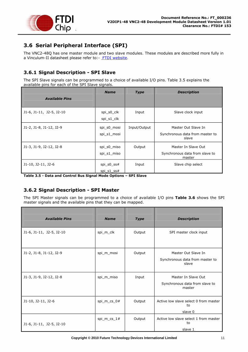
3.7.2 Timing Diagram – Asynchronous FIFO Mode Read and Write Cycle
When in Asynchronous FIFO interface mode, the timing of a read and write operation on the FIFO interface is shown in Figure 3.4 and Table 3.8
Figure 3.4 – Asynchronous FIFO Mode Read and Write Cycle.
Time Description Min Max Unit
t1 RD# inactive to RXF# 1 14 ns t2 RXF# inactive after RD# cycle 100 - ns t3 RD# to Data 1 14 ns t4 RD# active pulse width 30 - ns
t5 RD# active after RXF# 0 - ns
t6 WR# active to TXE# inactive 1 14 ns t7 TXE# inactive after WR# cycle 100 - ns t8 DATA to TXE# active setup time 5 - ns t9 DATA hold time after WR# inactive 5 - ns t10 WR# active pulse width 30 - ns t11 WR# active after TXE# 0 - ns
Table 3.8 - Asynchronous FIFO Mode Read Cycle Timing
In asynchronous mode an external device can control data transfer driving FIFO_WR# and FIFO_RD# inputs. In contrast to synchronous mode, in asynchronous mode the 245 FIFO module generates the output enable EN# signal. EN# signal is effectively the read signal RD#.
Current byte is available to be read when FIFO_RD# goes low. When FIFO_RD# goes high, FIFO_RXF# output will also go high. It will only become low again when there is another byte to read.
When FIFO_WR# goes low FIFO_TXE# flag will always go high. FIFO_TXE# goes low again only when there is still space for data to be written in to the module.

`
Copyright © 2010 Future Technology Devices International Limited 14
Document Reference No.: FT_000236 V2DIP1-48 VNC2-48 Development Module Datasheet Version 1.01
Clearance No.: FTDI# 153
3.8 Parallel FIFO Interface-Synchronous Mode
The Parallel FIFO Synchronous mode has an eight bit data bus, individual read and write strobes, two hardware flow control signals, an output enable and a clock out.
The synchronous FIFO mode uses the parallel FIFO interface signals detailed in Table 3.7 and an additional two signals detailed in Table 3.9.
Available Pins
Name
Type
Description
J2-8, J2-4, J1-7, J1-14, J1-19, J2-18, J2-13
fifo_oe#
Output FIFO Output Enable
J2-7, J1-4, J1-8, J1-16, J1-20, J2-17 fifo_clkout Output
FIFO Output Enable
Table 3.9 - Data and Control Bus Signal Mode Options – Synchronous FIFO mode
3.8.1 Timing Diagram – Synchronous FIFO Mode Read and Write Cycle
When in Synchronous FIFO interface mode, the timing of a read and write operation on the FIFO interface are shown in Figure 3.5 and Table 3.10
Figure 3.5 - Synchronous FIFO Mode Read and Write Cycle

`
Copyright © 2010 Future Technology Devices International Limited 15
Document Reference No.: FT_000236 V2DIP1-48 VNC2-48 Development Module Datasheet Version 1.01
Clearance No.: FTDI# 153
Time Description Min Typical Max Unit
t1 CLKOUT period - 20.83 - ns t2 CLKOUT high period 9.38 10.42 11.46 ns t3 CLKOUT low period 9.38 10.42 11.46 ns t4 CLKOUT to RXF# 1 - 7.83 ns t5 CLKOUT to read DATA valid 1 - 7.83 ns t6 OE# to read DATA valid 1 - 7.83 ns
t7 CLKOUT to OE# 1 - 7.83 ns
t8 RD# setup time 12 - - ns
t9 RD# hold time 0 - - ns
t10 CLKOUT TO TXE# 1 - - ns
t11 Write DATA setup time 12 - - ns t12 Write DATA hold time 0 - - ns
t13 WR# setup time 12 - - ns
t14 WR# hold time 0 - - ns Table 3.10 - Synchronous FIFO Mode Read and Write Cycle Timing
In synchronous mode data can be transmitted to and from the FIFO module on each clock edge. An
external device synchronises to the CLKOUT output and it also has access to the output enable OE# input to control data flow. An external device should drive output enable OE# low before pulling RD# line down.
When bursts of data are to be read from the module RD# should be kept low. RXF# remains low when there is still data to be read. Similarly when bursts of data are to be written to the module WR# should be kept low. TXE# remains low when there is still space available for the data to be written

`
Copyright © 2010 Future Technology Devices International Limited 16
Document Reference No.: FT_000236 V2DIP1-48 VNC2-48 Development Module Datasheet Version 1.01
Clearance No.: FTDI# 153
3.9 Debugger Interface
The purpose of the debugger interface is to provide access to the VNC2 silicon/firmware debugger. The debug interface can be accessed by connecting a debug module to the J3 connector. This debug module will give access to the debugger through a USB connection to a PC via the Integrated Development Environment (IDE). The IDE is a graphical interface to the VNC2 software development tool-chain and
gives the following debug capabilities through the debugger interface: Flash Erase, Write and Program. Application debug - application code can have breakpoints, be single stepped and can be halted. Detailed internal debug - memory and register read/write access.
The Debugger Interface, and how to use it, is further described in the following applications Note
Vinculum-II Debug Interface Description
3.9.1 Signal Description - Debugger Interface
Table 3.11 shows the signals and pins description for the debugger interface pin header J3
Pin No.
Name
Name
On PCB
Type
Description
J3-1 IO0 DBG I/O Debugger Interface
J3-2 - [Key] - Not connected. Used to make sure that the debug module is connected correctly.
J3-3 GND GND PWR Module ground supply pin
J3-4 RESET# RST#
Input Can be used by an external device to reset the VNCL2. This pin is also used in combination with PROG# and the UART interface to program firmware into the VNC2.
J3-5 PROG# PRG# Input
This pin is used in combination with the RESET# pin and the UART interface to program firmware into the VNC2.
J3-6 5V0 VCC
PWR Input 5.0V module supply pin. This pin can be used to provide the 5.0V input to the V2DIP1-48 when the V2DIP1-48 is not powered from the USB connector (VBUS) or the debugger interface. Also connected to DIL connector pins J1-2, J1-3 and J1-9 and J3-6.
Table 3.11 - Signal Name and Description – Debugger Interface
`
Copyright © 2010 Future Technology Devices International Limited 17
Document Reference No.: FT_000236 V2DIP1-48 VNC2-48 Development Module Datasheet Version 1.01
Clearance No.: FTDI# 153
4 Firmware
4.1 Firmware Support V2DIP1-48 can be programmed with the customers own firmware or with pre-compiled firmware profiles to allow a designer to easily change the functionality of the chip.
4.2 Available Firmware
V2DAP firmware is currently available: USB Host for single Flash Disk and general purpose USB peripherals. Selectable UART, FIFO or SPI interface command monitor. please refer to:- FTDI website for
full details.
4.3 Firmware Upgrades
Refer to the debugger interface section which can be used to update the firmware.

`
Copyright © 2010 Future Technology Devices International Limited 18
Document Reference No.: FT_000236 V2DIP1-48 VNC2-48 Development Module Datasheet Version 1.01
Clearance No.: FTDI# 153
5 External circuit Configuration
5.1 Adding a second USB Port
The external circuit configuration for adding second USB host port, with the USB activity LED,
is shown below in Figure 5.1
Figure 5.1 Additional USB Port Configuration
`
Copyright © 2010 Future Technology Devices International Limited 19
Document Reference No.: FT_000236 V2DIP1-48 VNC2-48 Development Module Datasheet Version 1.01
Clearance No.: FTDI# 153
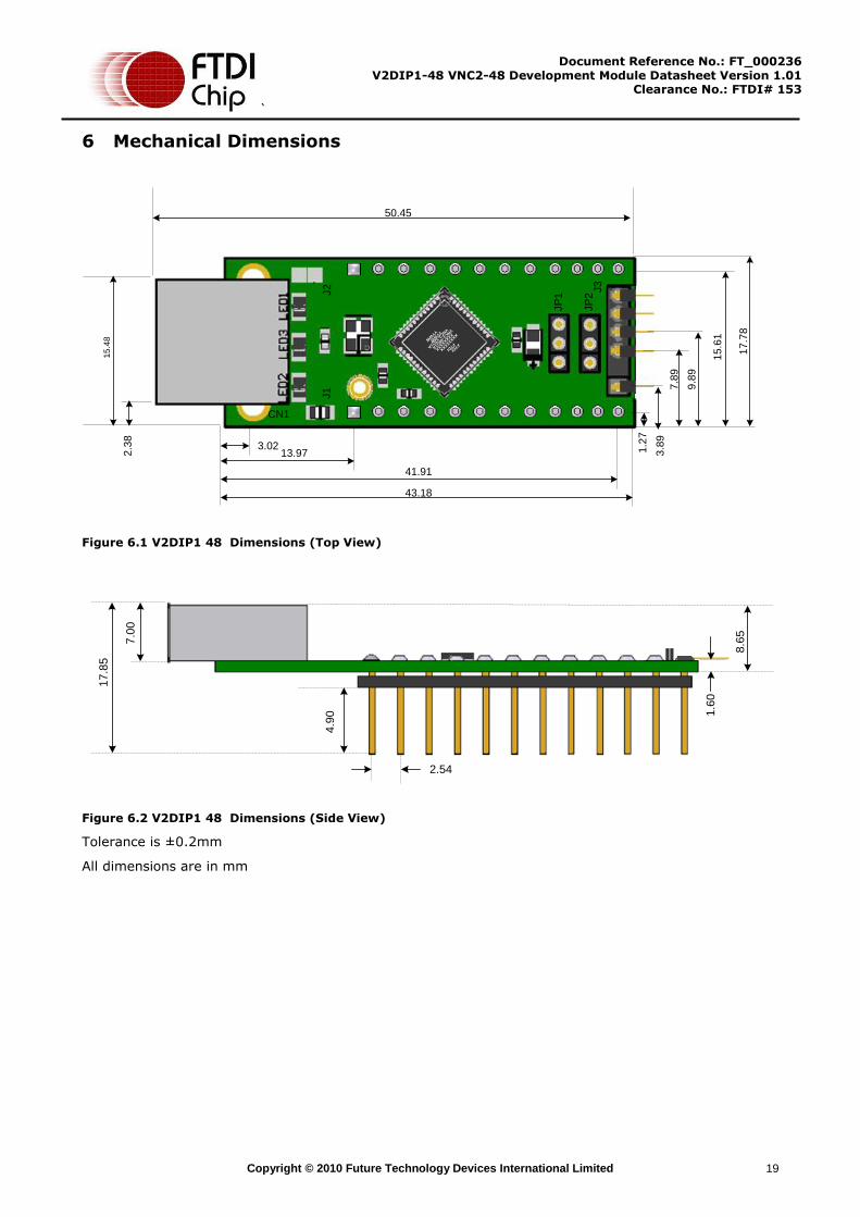
6 Mechanical Dimensions
3.02
3.8
9
1.2
7
2.3
8
FTDI
XX
XX
XX
XX
VN
C2-32Q
1A
YY
WW
J1
J2 J3
CN1
FTDI
XX
XX
XX
XX
VN
C2-48Q
1A
YY
WW
JP
1
JP
2
17
.78
15.6
1
9.8
9
7.8
9
15
.48
43.18
41.91
13.97
50.45
Figure 6.1 V2DIP1 48 Dimensions (Top View)
2.54
7.0
0
17
.85
1.6
0
4.9
0
8.6
5
Figure 6.2 V2DIP1 48 Dimensions (Side View)
Tolerance is ±0.2mm
All dimensions are in mm

`
Copyright © 2010 Future Technology Devices International Limited 20
Document Reference No.: FT_000236 V2DIP1-48 VNC2-48 Development Module Datasheet Version 1.01
Clearance No.: FTDI# 153
7 Schematic Diagram
Figure 7.1 - Schematic Diagram

`
Copyright © 2010 Future Technology Devices International Limited 21
Document Reference No.: FT_000236 V2DIP1-48 VNC2-48 Development Module Datasheet Version 1.01
Clearance No.: FTDI# 153
8 Contact Information
Head Office – Glasgow, UK Future Technology Devices International Limited Unit 1, 2 Seaward Place, Centurion Business Park Glasgow, G41 1HH United Kingdom Tel: +44 (0) 141 429 2777 Fax: +44 (0) 141 429 2758
E-mail (Sales) [email protected] E-mail (Support) [email protected] E-mail (General Enquiries) [email protected] Web Site URL http://www.ftdichip.com Web Shop URL http://www.ftdichip.com
Branch Office – Taipei, Taiwan Future Technology Devices International Limited (Taiwan) 2F, No 516, Sec. 1 NeiHu Road Taipei 114 Taiwan, R.O.C. Tel: +886 (0) 2 8791 3570 Fax: +886 (0) 2 8791 3576 E-mail (Sales) [email protected] E-mail (Support) [email protected] E-mail (General Enquiries) [email protected] Web Site URL http://www.ftdichip.com
Branch Office – Hillsboro, Oregon, USA Future Technology Devices International Limited (USA) 7235 NW Evergreen Parkway, Suite 600 Hillsboro, OR 97123-5803 USA Tel: +1 (503) 547 0988 Fax: +1 (503) 547 0987 E-Mail (Sales) [email protected] E-Mail (Support) [email protected] Web Site URL http://www.ftdichip.com Branch Office – Shanghai, China
Future Technology Devices International Limited (China) Room 408, 317 Xianxia Road, ChangNing District, ShangHai, China Tel: +86 (21) 62351596 Fax: +86(21) 62351595 E-Mail (Sales): [email protected] E-Mail (Support): [email protected] E-Mail (General Enquiries): [email protected] Web Site URL http://www.ftdichip.com
Distributor and Sales Representatives
Please visit the Sales Network page of the FTDI Web site for the contact details of our distributor(s) and sales representative(s) in your country.
`
Copyright © 2010 Future Technology Devices International Limited 22
Document Reference No.: FT_000236 V2DIP1-48 VNC2-48 Development Module Datasheet Version 1.01
Clearance No.: FTDI# 153
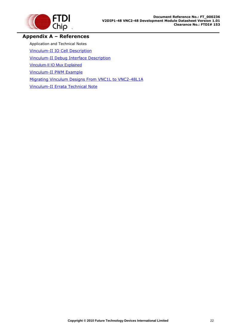
Appendix A – References
Application and Technical Notes
Vinculum-II IO Cell Description
Vinculum-II Debug Interface Description
Vinculum-II IO Mux Explained
Vinculum-II PWM Example
Migrating Vinculum Designs From VNC1L to VNC2-48L1A
Vinculum-II Errata Technical Note

`
Copyright © 2010 Future Technology Devices International Limited 23
Document Reference No.: FT_000236 V2DIP1-48 VNC2-48 Development Module Datasheet Version 1.01
Clearance No.: FTDI# 153
Appendix B – List of Figures and Tables
List of Figures
Figure 1.1- V2DIP1 48 ................................................................................................................... 1
Figure 3.1 - V2DIP1 48 Module Pin Out (Top View) .......................................................................... 4
Figure 3.2 - V2DIP1 48 Module Pin Out (Bottom View) .................................................................... 5
Figure 3.3 - V2DIP1 48 On-Board Jumper Pin Configuration. .............................................................. 8
Figure 3.4 – Asynchronous FIFO Mode Read and Write Cycle. ........................................................... 13
Figure 3.5 - Synchronous FIFO Mode Read and Write Cycle .............................................................. 14
Figure 5.1 Additional USB Port Configuration .................................................................................. 18
Figure 6.1 V2DIP1 48 Dimensions (Top View) ................................................................................ 19
Figure 6.2 V2DIP1 48 Dimensions (Side View) ............................................................................... 19
Figure 7.1 - Schematic Diagram ................................................................................................... 20
List of Tables
Table 3.1 - Pin Signal Descriptions .................................................................................................. 6
Table 3.2 - V2DIP1 48 Port Selection Jumper Pins ............................................................................. 8
Table 3.3 - Default Interface I/O Pin Configuration ........................................................................... 9
Table 3.4 - Data and Control Bus Signal Mode Options – UART Interface ........................................... 10
Table 3.5 - Data and Control Bus Signal Mode Options – SPI Slave ................................................... 11
Table 3.6 - Data and Control Bus Signal Mode Options – SPI Master ................................................. 12
Table 3.7 - Data and Control Bus Signal Mode Options – Parallel FIFO Interface ................................. 12
Table 3.8 - Asynchronous FIFO Mode Read Cycle Timing .................................................................. 13
Table 3.9 - Data and Control Bus Signal Mode Options – Synchronous FIFO mode .............................. 14
Table 3.10 - Synchronous FIFO Mode Read and Write Cycle Timing ................................................... 15
Table 3.11 - Signal Name and Description – Debugger Interface ....................................................... 16

`
Copyright © 2010 Future Technology Devices International Limited 24
Document Reference No.: FT_000236 V2DIP1-48 VNC2-48 Development Module Datasheet Version 1.01
Clearance No.: FTDI# 153
Appendix C – Revision History
Version 1.0 First Release 16th April 2010
Version 1.01 Added module’s images, edited mechanical drawings and 24th May 2010
Figure 5.1
Recommended