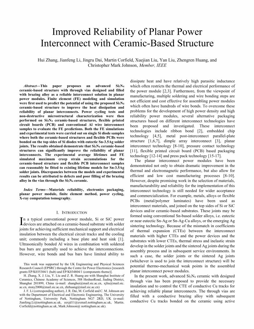
Zhang, Hui and Li, Jianfeng and Dai, Jingru and Corfield, Martin and Liu, Xuejian and Liu, Yan and Huang, Zhengren and Johnson, Christopher Mark (2018) Improved reliability of planar power interconnect with ceramic-based structure. IEEE Journal of Emerging and Selected Topics in Power Electronics, 6 (1). pp. 175-187. ISSN 2168-6785
Access from the University of Nottingham repository: http://eprints.nottingham.ac.uk/46782/1/Improved%20Reliability%20of%20Planar%20Power%20Interconnect%20with%20Ceramic-Based%20Structure.pdf
Copyright and reuse:
The Nottingham ePrints service makes this work by researchers of the University of Nottingham available open access under the following conditions.
This article is made available under the University of Nottingham End User licence and may be reused according to the conditions of the licence. For more details see: http://eprints.nottingham.ac.uk/end_user_agreement.pdf
A note on versions:
The version presented here may differ from the published version or from the version of record. If you wish to cite this item you are advised to consult the publisher’s version. Please see the repository url above for details on accessing the published version and note that access may require a subscription.
For more information, please contact [email protected]
Abstract—This paper proposes an advanced Si3N4
ceramic-based structure with through vias designed and filled
with brazing alloy as a reliable interconnect solution in planar
power modules. Finite element (FE) modeling and simulation
were first used to predict the potential of using the proposed Si3N4
ceramic-based structure to improve the heat dissipation and
reliability of planar interconnects. Power cycling tests and
non-destructive microstructural characterization were then
performed on Si3N4 ceramic-based structures, flexible printed
circuit boards (PCB) and conventional Al wire interconnect
samples to evaluate the FE predictions. Both the FE simulations
and experimental tests were carried out on single Si diode samples
where both the ceramic-based structures and flexible PCBs were
bonded on the top sides of Si diodes with eutectic Sn-3.5Ag solder
joints. The results obtained demonstrate that Si3N4 ceramic-based
structures can significantly improve the reliability of planar
interconnects. The experimental average lifetimes and FE
simulated maximum creep strain accumulations for the
ceramic-based structure and flexible PCB interconnect samples
can reasonably be fitted to existing lifetime models for Sn-3.5Ag
solder joints. Discrepancies between the models and experimental
results can be attributed to defects and poor filling of the brazing
alloy in the vias through the Si3N4 ceramic.
Index Terms—Materials reliability, electronics packaging,
planar power module, finite element method, power cycling,
X-ray computation tomography.
I. INTRODUCTION
n a typical conventional power module, Si or SiC power
devices are attached on a ceramic-based substrate with solder
joints for achieving sufficient mechanical support and electrical
insulation between the electrical circuit tracks and the cooling
unit; commonly including a base plate and heat sink [1].
Ultrasonically bonded Al wires in combination with soldered
bus bars are generally used to achieve the interconnections.
However, wire bonds and bus bars have limited ability to
This work was supported by the UK Engineering and Physical Sciences
Research Council (EPSRC) through the Centre for Power Electronics [research grants EP/K035304/1 (hub) and EP/K034804/1 (components theme)].
H. Zhang, X. J. Liu, Y. Liu and Z. R. Huang are with Shanghai Institute of
Ceramics, Chinese Academy of Sciences, 588 HeshuoRoad, Jiading District, Shanghai 201899, China (e-mail: [email protected], [email protected].
ac.cn, [email protected], [email protected])
J. F. Li (corresponding author), J. R. Dai, M. Corfield and C. M. Johnson are with the Department of Electrical and Electronic Engineering, The University
of Nottingham, University Park, Nottingham NG7 2RD, UK (e-mail:
[email protected], [email protected], Martin. [email protected], Mark.Johnson@ nottingham.ac.uk).
dissipate heat and have relatively high parasitic inductance
which often restricts the thermal and electrical performance of
the power module [2,3]. Furthermore, from the viewpoint of
manufacturing, multiple soldering and wire bonding steps are
not efficient and cost effective for assembling power modules
which often have hundreds of wire bonds. To overcome these
problems for the development of high power density and high
reliability power modules, several alternative packaging
structures based on different interconnect technologies have
been proposed and investigated. These interconnect
technologies include ribbon bond [2], embedded chip
technology [4,5], metal post-interconnect parallel-plate
structure [1,6,7], dimple array interconnect [3], planar
interconnect technology [8-10], pressure contact technology
[11], flexible printed circuit board (PCB) based packaging
technology [12-14] and press pack technology [15-17].
The planar interconnect power modules have been
demonstrated not only to obtain dramatic improvement in the
thermal and electromagnetic performance, but also allow for
efficient and low cost manufacturing processes [8-10].
However, despite promising work in the selection of materials,
manufacturability and reliability for the implementation of this
interconnect technology is still needed for wider acceptance
and commercialization. For example, metals, alloys or flexible
PCBs (metal/polymer laminates) have been used as
interconnect materials, and joined on the top sides of Si or SiC
devices and/or ceramic-based substrates. These joints may be
formed using conventional Sn-based solder alloys, i.e. eutectic
or near eutectic Sn-Ag or Sn-Ag-Cu alloys, or the emerging Ag
sintering technology. Because of the mismatch in coefficients
of thermal expansion (CTEs) between the interconnect
materials with higher CTEs and the power devices and the
substrates with lower CTEs, thermal stress and inelastic strain
develop in the solder joints and the sintered Ag joints during the
assembly process and in subsequent service environments. In
such a case, the solder joints or the sintered Ag joints
(whichever is used to join the interconnect structure) will be
potential thermo-mechanical weak points in the assembled
planar interconnect power modules.
In the present work, advanced Si3N4 ceramic with designed
through vias has been proposed to provide the necessary
insulation and to control the CTE of conductive Cu tracks for
achieving reliable planar interconnects. The through vias are
filled with a conductive brazing alloy with subsequent
conductive Cu tracks bonded on the ceramic using active
Improved Reliability of Planar Power
Interconnect with Ceramic-Based Structure
Hui Zhang, Jianfeng Li, Jingru Dai, Martin Corfield, Xuejian Liu, Yan Liu, Zhengren Huang, and
Christopher Mark Johnson, Member, IEEE
I
brazing technology. The main objective of this paper is to
demonstrate the reliability of such an innovative ceramic-based
interconnect technology through comparison with conventional
Al wire bond technology and flexible PCB interconnect
technology under similar power cycling conditions. A
comparison has been carried out using both finite element (FE)
simulations and experimental tests on single Si diode samples
where both the ceramic-based and flexible PCB interconnects
were bonded on the top sides of Si diodes with eutectic
Sn-3.5Ag solder joints. However, the results obtained can
readily be applied to power modules which contain multiple
power devices constructed with these interconnect
technologies.
II. FINITE ELEMENT MODELING AND SIMULATION
Before preparation of any samples, FE thermal and
thermo-mechanical modeling and simulation have been used to
predict the potential of the proposed Si3N4 ceramic-based
structure to improve the heat dissipation and reliability of
planar interconnects using commercial available finite element
(FE) analysis software Abaqus 6.14-1 and its graphic user
interface CAE.
(a)
(b)
(c)
Fig. 1. Computer aided design graphs of the single Si diode samples with the three types of interconnect technologies (a) Al wire; (b) flexible PCB; and (c)
Si3N4 ceramic-based structure.
A. Description of Samples for Power Cycling Tests
The present work is mainly concerned with ceramic-based
interconnect technology, where conventional Al wire bonding
and emerging flexible PCB interconnect technologies are
employed as benchmarks. Fig. 1 shows computer aided design
images of single Si diode samples which are constructed with
the three interconnect technologies for both the FE simulation
and the power cycling tests. For all samples, the Si diode is
attached on an AlN-based substrate with 100 µm thick
Sn-3.5Ag solder joint. The Si diode is 13.5 mm × 13.5 mm ×
0.5 mm in size, and the AlN-based substrate is 58.2 mm 49.5
mm × 1 mm thick AlN ceramic tile with 0.3 mm thick Cu tracks
actively brazed on both sides.
For each of the Al wire bond interconnect samples, 10 Al
wires (375 µm in diameter) are bonded on the top anode of the
diode at one end, and on the substrate at the other end. In each
of the flexible PCB interconnect samples, a 13.5 mm × 13.5
mm × 0.5 mm Cu post is attached with a 100 µm thick
Sn-3.5Ag solder joint on a Cu island of the substrate. A 30 mm
13.5 mm flexible PCB is soldered on the top sides of both the
Si diode and the Cu post with Sn-3.5Ag solder joints for
achieving the interconnect, where the thickness of the solder
joints is also 100 µm. The flexible PCB consists of 100 µm
thick polyimide laminated with 50 µm thick Cu tracks on both
sides. As shown in Fig. 2(a), the vias (0.5 mm in diameter) in
the flexible PCB are through the bottom Cu tracks and the
polyimide layer, and are filled with Sn-3.5Ag solder alloy.
(a)
(b)
Fig. 2. Cross-sectional schematics of thesingle Si diode samples with planar interconnects: (a) flexible PCB; and (b) ceramic-based structure.
As shown in Fig. 2(b), in each of the ceramic-based
interconnect samples, a Si3N4 ceramic-based structure is
soldered on the top sides of both the Si diode and a Cu post with
100 µm thick Sn-3.5Ag solder joints. The Si3N4 ceramic tile is
selected due to its high strength and thermo-mechanical
reliability. It is 0.3 mm in thickness, and the through vias (0.5
mm in diameter) are filled with a conductive brazing alloy with
subsequent conductive Cu tracks bonded on to it using active
brazing technology. The brazing alloy is Ag-35.25Cu-1.75Ti,
and 0.05, 0.1 and 0.2 mm thick Cu tracks are considered. The
different combinations of Cu tracks and insulation/support
layers considered for the flexible PCB and the Si3N4
ceramic-based ceramic structures are listed in Table I.
TABLE I
CODES AND THE CORRESPONDING COMBINATIONS OF CU TRACKS AND INSULATION/SUPPORT LAYERS IN THE FLEXIBLE PCB AND CERAMIC-BASED STRUCTURE
Code Bottom Cu tracks Insulation/support Top Cu tracks Via filling
Flex PCB 0.05 mm thick Cu 0.1 mm thick polyimide 0.05 mm thick Cu
ACT1 0.1 mm thick Cu 0.3 mm thick Si3N4 with true CTE of 3 ppm/C 0.1 mm thick Cu Perfect
ACT2 0.2 mm thick Cu 0.3 mm thick Si3N4 with true CTE of 3 ppm/C 0.2 mm thick Cu Perfect
ACT3 0.1 mm thick Cu 0.3 mm thick Si3N4 with true CTE of 3 ppm/C 0.1 mm thick Cu Imperfect
ACT4 0.05 mm thick Cu 0.3 mm thick Si3N4 with true CTE of 3 ppm/C 0.2 mm thick Cu Perfect
ACT5 0.1 mm thick Cu 0.3 mm thick Si3N4 with assumed CTE of 6 ppm/C 0.1 mm thick Cu Perfect
ACT6 0.1 mm thick Cu 0.3 mm thick Si3N4 with assumed CTE of 9 ppm/C 0.1 mm thick Cu perfect
It should be noted that AlN ceramic which has a higher
thermal conductivity and is more commonly used as a support
substrate in power electronic packaging is not suitable for
forming through vias designed and filled with brazing alloy.
This is because it has a relatively weak mechanical strength,
and is easily broken during laser drilling/cutting to produce the
through vias. In previous work [18], Si3N4-based substrates
with 4 through vias mechanically filled with Cu cylinders were
used to construct planar half bridge modules. However, the vias
were not directly on the top sides of the power devices, and the
reliability of the constructed modules were not tested.
On the other hand, it is well known that Si3N4 ceramic has
better reliability but poorer thermal performance than AlN
ceramic under similar thermo-mechanical loads. The present
work is concerned with the reliability of top side interconnects
of 0.5 mm thick Si diodes which have been attached on
AlN-based substrates. In the case of conventional Al wire
bonds as top side interconnects, failure is dominated by the
in-elastic strain development in the Al wire bond due to
mismatch of CTEs between Al and Si. If the substrate is
changed to thinner Si3N4 ceramic (i.e. 0.32 mm or 0.64 mm
thick) from thicker AlN ceramic (i.e. 1 mm thick), heating
current pulses with lower amplitude have to be used for
achieving similar temperature profiles during the power cycling
tests, while the in-elastic strain development and hence the
reliability of the Al wire bonds would remain similar.
B. FE Models
For all the single Si diode samples described above, FE
thermal models have been developed to simulate the
temperature fields during 50 power cycles. In each sample, the
top one third thickness of the Si diode was considered as the
active region generating electrical heat, and two different
volumetric heating sources were considered. The latter being
the product of 50 current pulses with an amplitude of 90 A
multiplied by the voltage drop across either a 2.5 kV Si diode
(referred to as lower power diode because of lower forward
voltage drop and power dissipation) or a 4.5 kV Si diode
(referred to as higher power diode because of higher forward
voltage drop and power dissipation) during the power cycling
test. For each of the two heating sources, the on time and off
time during every current pulse was determined by achieving
40 C and 120 C as the low and high limits of the average
temperatures on the hottest 5 mm × 5 mm top surface area on
the sample. A convection heat exchange condition with a heat
exchange coefficient of 575 Wm-2k-1 was applied on the
bottom surface of the AlN-based substrate.
The thermo-mechanical model is mainly concerned with the
stress/strain developments within the solder joints in the
flexible PCB and ceramic-based interconnect samples. During
the simulation, each of the samples was first subjected to a
predefined temperature profile of 192C down to 25 C within
3 min to simulate the reflow process. The initial heating up
stage of the reflow process was found to have negligible effects
on the simulated stress/strain development in solder joints [19]
and was therefore not considered. The eutectic Sn-3.5Ag solder
alloy has a melting point of 221 ºC, and the solidification of the
molten solder generally occurs at a super-cooling temperature
of 192 ºC [20]. The temperature field simulated with the
aforementioned thermal model was then used as inputs to
simulate the further stress/strain developments in the sample
during the 50 current pulses.
(a)
(b)
Fig. 3. A representative meshing system to discretize a ceramic-based
interconnect sample: (a) overview; and (b) locally enlarged view.
Similar meshing systems were employed to discretize all the
samples, and the same meshing system was used for the thermal
model and the thermo-mechanical models where applicable.
Fig. 3 presents a representative meshing system consisting of
481820 DC3D6E linear triangular prism elements and C3D4
linear tetrahedron elements to discretize one ceramic-based
interconnect sample. The smallest and the largest element sizes
in the plane directions of the substrate are respectively 0.25 mm
and 1 mm, and the smallest and the largest element sizes in the
through-thickness direction are respectively 0.025 mm and
0.428 mm. In all the simulation cases, the elements used in the
critical domains all have the same dimensions. For example, the
sizes of the triangular prism elements used to discretize the
critical solder joints whose maximum von Mises stress and
creep strain accumulation will be used to assess the
thermo-mechanical reliability are all 0.25 mm in the plane
directions, and 0.025 m in the through-thickness direction. This
is necessary because longer computing times would be required
if meshing size-independent solutions were implemented for
the present three-dimensional model with a much finer meshing
system. Therefore, relatively coarse meshing systems with the
same size of elements (in the critical domains for all the
simulation cases) have been employed to achieve acceptable
computing times.
The thermal and thermo-mechanical properties of the
polyimide in the flexible PCB and the Si3N4 ceramic and
brazing alloys in the ceramic–based structures are given in
Table II. The brazing alloy between the Cu and AlN ceramic
tile is ignored. The properties of the other materials used for the
simulations were taken from existing literature [21-23], and are
not repeated here. Of them, Chaboche’s plastic model was used
to describe the mechanical properties of both Al and Cu, and
Anand’s creep model was used to describe the mechanical
properties of the Sn-3.5Ag solder joints. Only elastic
deformation was considered for Si and AlN in all the samples.
TABLE II
THERMAL AND THERMO-PHYSICAL PROPERTIES OF PART MATERIALS IN THE
SINGLE SI DIODE SAMPLES
Polyimide Si3N4 Ag35.25Cu1.75Ti
Thermal conductivity (WK-1m-1) 0.12 90 180
Specific heat (Jkg-1C-1) 1150 691 292
Density (kgcm-3) 1.43 3.20 9.80
Young’s modulus (GPa) 3.2 312 83
Poisson ratio 0.34 0.27 0.30
Yield strength (MPa) 271
Tensile/flexual strength (MPa) 700 346
Elongation (%) 20
CTE (ppmC-1) 11.6+0.12T 3.0 18.5
T is temperature in C.
For the Al wire bonds, flexible PCB and ceramic-based
structures ACT1 and ACT2 interconnect samples, both lower
and higher power Si diodes were considered, and the
simulations are referred to as main simulations. For the
ceramic-based structures ACT3, ACT4, ACT5 and ACT6, only
higher power Si diode were taken, and the simulations are
referred to as additional simulations. All the thermal and
thermo-mechanical simulations have been executed on a PC
computer with Intel[R] Core[TM] i7-3820 CPU @ 3.60 GHz
processor and 64 GB RAM. The running times for the thermal
simulations were approximately 2 hours and for the
thermo-mechanical simulations 33 to 48 hours for all cases.
C. FE Simulation Results
During the thermal simulation, the heat is generated within
the active region of the Si diode, and hence this region is at a
higher temperature than the rest of the regions in the sample.
During the early stage of the transient simulation, the low and
high limits of the average temperatures on the hottest 5 mm × 5
mm top surface area of all the samples were somewhat lower
and gradually increased with increasing number of power
cycles (current pulse with an amplitude of 90 A). After about 60
s of the transient simulation, they all reached the specified 40
C and 120 C during every power cycle. Fig. 4 shows one
example of the simulated distribution of the temperatures in a
sample during one such power cycle. Fig. 5 presents the heating
power (heating source during the simulation) and the simulated
evolution of the cyclic average temperatures on the hottest 5
mm × 5 mm top surface area of the flexible PCB interconnect
sample for both lower power Si diode and higher power Si
diode.
Fig. 4. The simulated distribution of temperature in the hottest ACT1
interconnected sample during one power cycle, where the Si diode is a lower
power diode.
Figure 6 compares the on time and off time of the pulse
current during every power cycle for the samples with both
lower power diode and higher power diode to achieve the
specified 40 C and 120 C as the low and high limits of the
average temperatures on the hottest 5 mm × 5 mm top surface
area of the assembled samples. It can be seen that with lower
power Si diode, the flexible PCB interconnect sample has an on
time and off time similar to those of an Al wire interconnect
sample. By contrast, the ceramic-based interconnect samples
can increase the on time by 28% to 38%, and increase the off
time by 28% to 30%. With higher power Si diode, the flexible
PCB interconnect sample can slightly increase both the on time
and off time by 8% compared to the Al wire interconnect
sample. In comparison the ceramic-based interconnect samples
can increase the on time by 34% to 52%, and the off time by
22% to 28% to an Al wire interconnect sample. The present
thermal simulation has fixed the low and high limits of the
temperatures. Therefore if all the samples are subjected to the
same current pulses, i.e. the same heating power, the
ceramic-based interconnect samples would reduce the chip
temperatures when compared with Al wire and flexible PCB
interconnect samples. It should be iterated that in the thermal
simulation the heat is assumed to be removed from the bottom
side of the AlN-based substrate for all the samples. Therefore, it
can be concluded that the ceramic-based interconnects indeed
improve the ability of the samples to dissipate heat.
(a)
(b)
Fig. 5. Thermal simulation results of the flexible PCB interconnect sample
with both lower power and high power Si diodes: (a) heating power; and (b)
evolution of the cyclic average temperatures on the hottest 5 mm × 5 mm top
surface area.
The thermo-mechanical simulation results indicate that in all
the as-reflowed samples, the maximum Mises stress and
maximum creep strain accumulation occur in the solder joints
used to attach the Cu posts on the AlN-based DBC substrates.
This can be ascribed to the mismatch of CTEs between the Cu
post and DBC substrate. During the power cycling, the
maximum stress and creep strain accumulation have been
moved to the solder joint used to bond the flexible PCB or the
Si3N4 ceramic-based structures on the top sides of the diodes in
all the simulation cases, especially near the interface between
the solder and the Si diode. This can be explained by the higher
cyclic temperatures encountered by this solder joint as shown in
Fig. 4, while both the flexible PCB and the Si3N4 ceramic-based
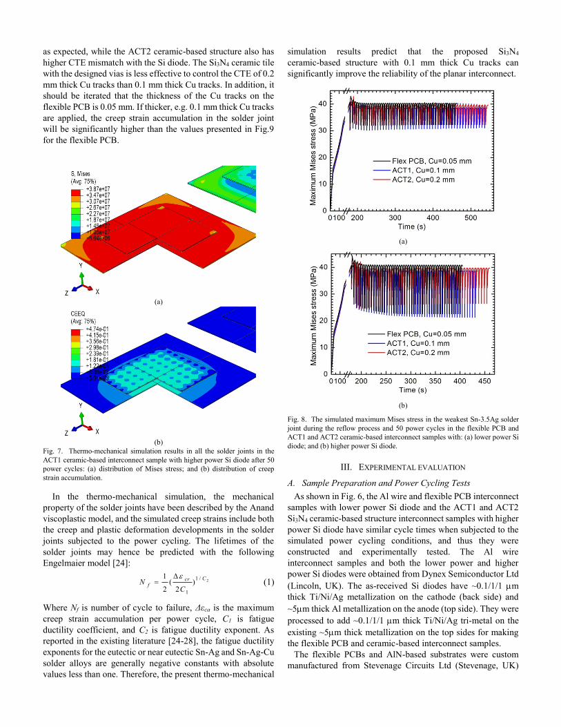
structures still have higher CTEs than the Si diodes. Fig. 7
presents the simulated distributions of Mises stress and creep
strain accumulation in all the solder joints in the ACT1
ceramic-based interconnect sample after 50 power cycles. The
solder joint with the maximum Mises stress and the maximum
creep strain accumulation is hence identified as the weakest
solder joint.
(a)
(b)
Fig. 6. Comparison of on time and off time of pulse current during every power
cycle for the different samples with: (a) lower power Si diode; and (b) higher
power Si diode to achieve the specified temperature profile.
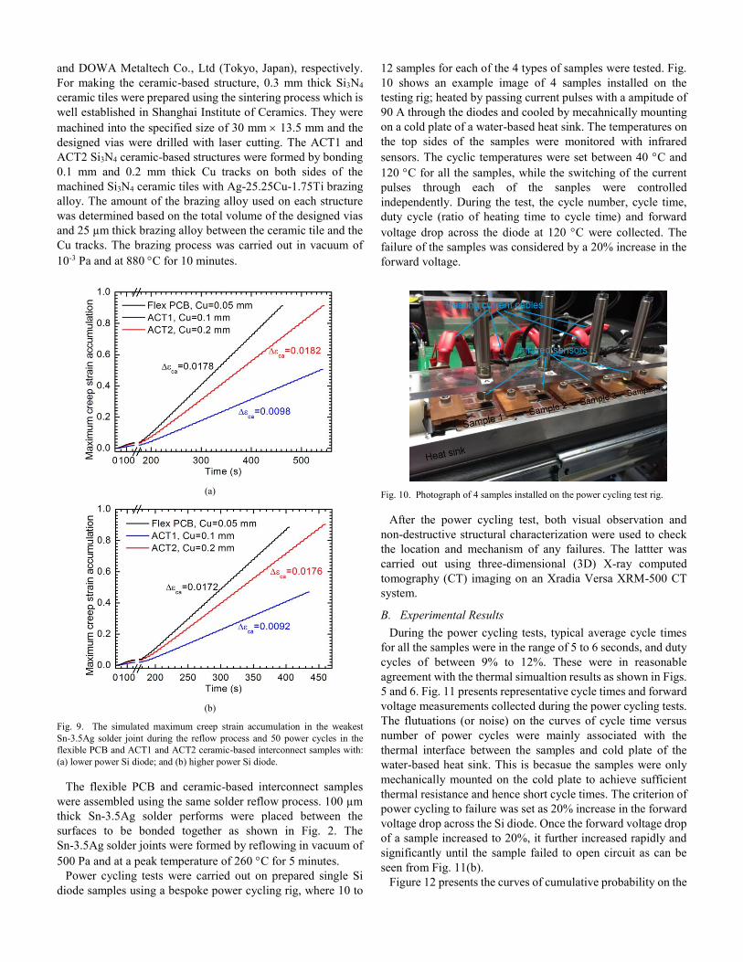
Figures 8 and 9 further compare the evolutions of the
maximum Mises stress and the maximum creep strain
accumulation in the weakest Sn-3.5Ag solder joint in all main
simulations, where Δεca stands for the stable creep strain
accumulation per power cycle. It can be seen that the cyclic
range of the maximum Mises stress in the solder joint is
remarkably affected by the cycle time. The sample with higher
power Si diode and shorter cycle period has larger cyclic range
of the maximum Mises stress than the corresponding sample
with lower power Si diode and longer cycle period. This can
readily be understood because the solder joints experience
relatively low time-dependant creep deformation and relatively
high elastic recovery with shorter cycle time than with longer
cycle time.
By contrast, the maximum creep strain accumulation is more
remarkably affected by the interconnect material and structure.
The maximum creep strain accumulation per power cycle in the
weakest solder joint in the sample with ACT1 ceramic-based
structure is almost 50% lower than that in the samples with
flexible PCB and ACT2 ceramic-based structure. This result
can be attributed to the fact that the creep strain development
within the solder joint is closely associated with the CTE
mismatch between the interconnect structure and the Si diode.
The flexible PCB has higher CTE mismatch with the Si diode
as expected, while the ACT2 ceramic-based structure also has
higher CTE mismatch with the Si diode. The Si3N4 ceramic tile
with the designed vias is less effective to control the CTE of 0.2
mm thick Cu tracks than 0.1 mm thick Cu tracks. In addition, it
should be iterated that the thickness of the Cu tracks on the
flexible PCB is 0.05 mm. If thicker, e.g. 0.1 mm thick Cu tracks
are applied, the creep strain accumulation in the solder joint
will be significantly higher than the values presented in Fig.9
for the flexible PCB.
(a)
(b)
Fig. 7. Thermo-mechanical simulation results in all the solder joints in the
ACT1 ceramic-based interconnect sample with higher power Si diode after 50
power cycles: (a) distribution of Mises stress; and (b) distribution of creep
strain accumulation.
In the thermo-mechanical simulation, the mechanical
property of the solder joints have been described by the Anand
viscoplastic model, and the simulated creep strains include both
the creep and plastic deformation developments in the solder
joints subjected to the power cycling. The lifetimes of the
solder joints may hence be predicted with the following
Engelmaier model [24]:
2/1
1
)2
(2
1 Ccrf
CN
(1)
Where Nf is number of cycle to failure, Δεca is the maximum
creep strain accumulation per power cycle, C1 is fatigue
ductility coefficient, and C2 is fatigue ductility exponent. As
reported in the existing literature [24-28], the fatigue ductility
exponents for the eutectic or near eutectic Sn-Ag and Sn-Ag-Cu
solder alloys are generally negative constants with absolute
values less than one. Therefore, the present thermo-mechanical
simulation results predict that the proposed Si3N4
ceramic-based structure with 0.1 mm thick Cu tracks can
significantly improve the reliability of the planar interconnect.
(a)
(b)
Fig. 8. The simulated maximum Mises stress in the weakest Sn-3.5Ag solder
joint during the reflow process and 50 power cycles in the flexible PCB and
ACT1 and ACT2 ceramic-based interconnect samples with: (a) lower power Si
diode; and (b) higher power Si diode.
III. EXPERIMENTAL EVALUATION
A. Sample Preparation and Power Cycling Tests
As shown in Fig. 6, the Al wire and flexible PCB interconnect
samples with lower power Si diode and the ACT1 and ACT2
Si3N4 ceramic-based structure interconnect samples with higher
power Si diode have similar cycle times when subjected to the
simulated power cycling conditions, and thus they were
constructed and experimentally tested. The Al wire
interconnect samples and both the lower power and higher
power Si diodes were obtained from Dynex Semiconductor Ltd
(Lincoln, UK). The as-received Si diodes have ~0.1/1/1 m
thick Ti/Ni/Ag metallization on the cathode (back side) and
~5m thick Al metallization on the anode (top side). They were
processed to add ~0.1/1/1 m thick Ti/Ni/Ag tri-metal on the
existing ~5m thick metallization on the top sides for making
the flexible PCB and ceramic-based interconnect samples.
The flexible PCBs and AlN-based substrates were custom
manufactured from Stevenage Circuits Ltd (Stevenage, UK)
and DOWA Metaltech Co., Ltd (Tokyo, Japan), respectively.
For making the ceramic-based structure, 0.3 mm thick Si3N4
ceramic tiles were prepared using the sintering process which is
well established in Shanghai Institute of Ceramics. They were
machined into the specified size of 30 mm 13.5 mm and the
designed vias were drilled with laser cutting. The ACT1 and
ACT2 Si3N4 ceramic-based structures were formed by bonding
0.1 mm and 0.2 mm thick Cu tracks on both sides of the
machined Si3N4 ceramic tiles with Ag-25.25Cu-1.75Ti brazing
alloy. The amount of the brazing alloy used on each structure
was determined based on the total volume of the designed vias
and 25 µm thick brazing alloy between the ceramic tile and the
Cu tracks. The brazing process was carried out in vacuum of
10-3 Pa and at 880 C for 10 minutes.
(a)
(b)
Fig. 9. The simulated maximum creep strain accumulation in the weakest
Sn-3.5Ag solder joint during the reflow process and 50 power cycles in the
flexible PCB and ACT1 and ACT2 ceramic-based interconnect samples with:
(a) lower power Si diode; and (b) higher power Si diode.
The flexible PCB and ceramic-based interconnect samples
were assembled using the same solder reflow process. 100 µm
thick Sn-3.5Ag solder performs were placed between the
surfaces to be bonded together as shown in Fig. 2. The
Sn-3.5Ag solder joints were formed by reflowing in vacuum of
500 Pa and at a peak temperature of 260 C for 5 minutes.
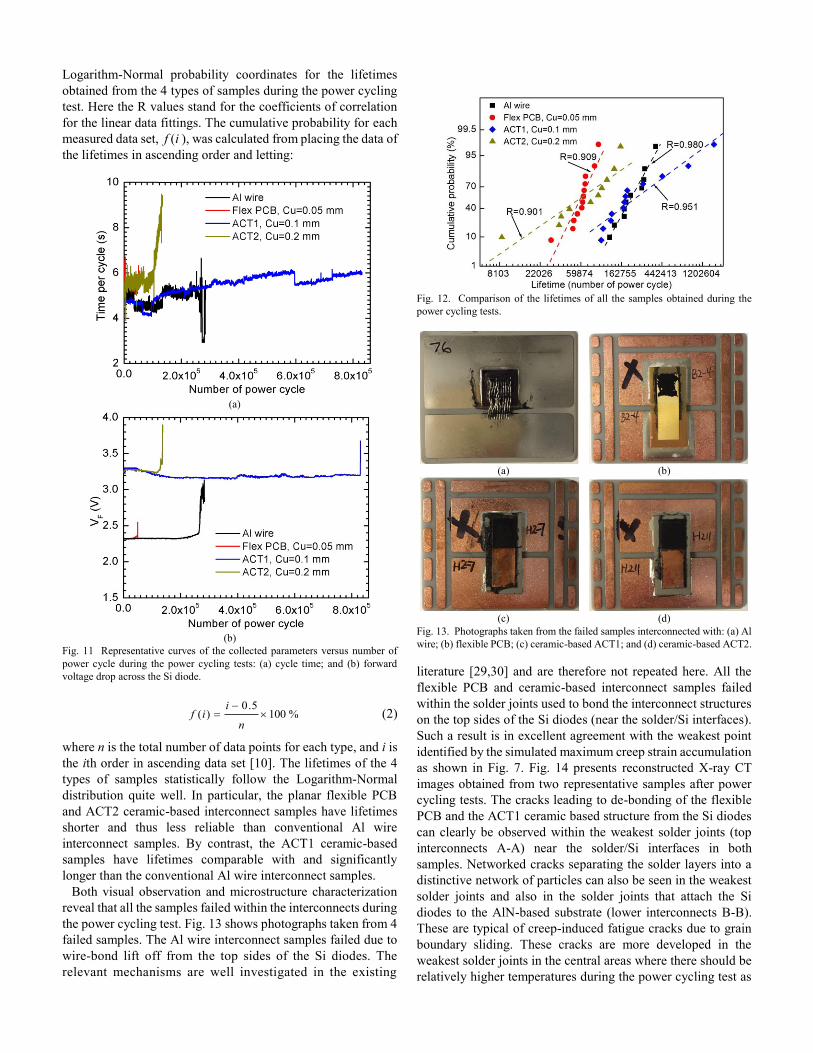
Power cycling tests were carried out on prepared single Si
diode samples using a bespoke power cycling rig, where 10 to
12 samples for each of the 4 types of samples were tested. Fig.
10 shows an example image of 4 samples installed on the
testing rig; heated by passing current pulses with a ampitude of
90 A through the diodes and cooled by mecahnically mounting
on a cold plate of a water-based heat sink. The temperatures on
the top sides of the samples were monitored with infrared
sensors. The cyclic temperatures were set between 40 C and
120 C for all the samples, while the switching of the current
pulses through each of the sanples were controlled
independently. During the test, the cycle number, cycle time,
duty cycle (ratio of heating time to cycle time) and forward
voltage drop across the diode at 120 C were collected. The
failure of the samples was considered by a 20% increase in the
forward voltage.
Fig. 10. Photograph of 4 samples installed on the power cycling test rig.
After the power cycling test, both visual observation and
non-destructive structural characterization were used to check
the location and mechanism of any failures. The lattter was
carried out using three-dimensional (3D) X-ray computed
tomography (CT) imaging on an Xradia Versa XRM-500 CT
system.
B. Experimental Results
During the power cycling tests, typical average cycle times
for all the samples were in the range of 5 to 6 seconds, and duty
cycles of between 9% to 12%. These were in reasonable
agreement with the thermal simualtion results as shown in Figs.
5 and 6. Fig. 11 presents representative cycle times and forward
voltage measurements collected during the power cycling tests.
The flutuations (or noise) on the curves of cycle time versus
number of power cycles were mainly associated with the
thermal interface between the samples and cold plate of the
water-based heat sink. This is becasue the samples were only
mechanically mounted on the cold plate to achieve sufficient
thermal resistance and hence short cycle times. The criterion of
power cycling to failure was set as 20% increase in the forward
voltage drop across the Si diode. Once the forward voltage drop
of a sample increased to 20%, it further increased rapidly and
significantly until the sample failed to open circuit as can be
seen from Fig. 11(b).
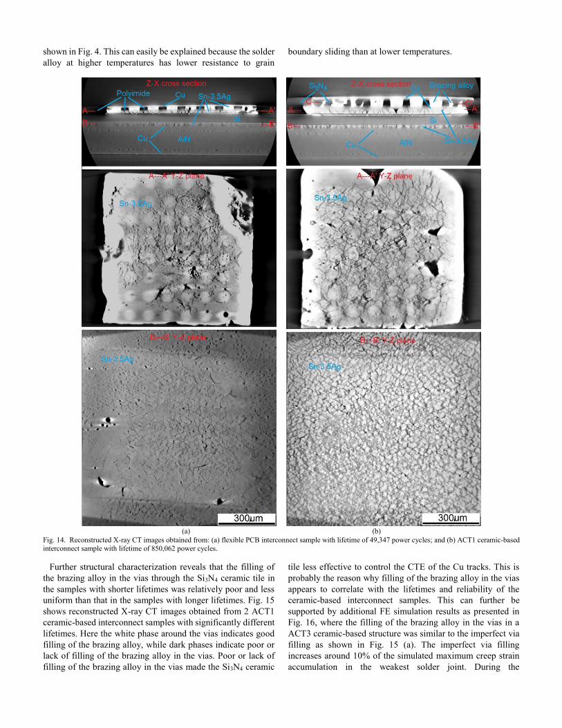
Figure 12 presents the curves of cumulative probability on the
Logarithm-Normal probability coordinates for the lifetimes
obtained from the 4 types of samples during the power cycling
test. Here the R values stand for the coefficients of correlation
for the linear data fittings. The cumulative probability for each
measured data set, f (i ), was calculated from placing the data of
the lifetimes in ascending order and letting:
(a)
(b)
Fig. 11 Representative curves of the collected parameters versus number of
power cycle during the power cycling tests: (a) cycle time; and (b) forward
voltage drop across the Si diode.
%1005.0
)(
n
iif (2)
where n is the total number of data points for each type, and i is
the ith order in ascending data set [10]. The lifetimes of the 4
types of samples statistically follow the Logarithm-Normal
distribution quite well. In particular, the planar flexible PCB
and ACT2 ceramic-based interconnect samples have lifetimes
shorter and thus less reliable than conventional Al wire
interconnect samples. By contrast, the ACT1 ceramic-based
samples have lifetimes comparable with and significantly
longer than the conventional Al wire interconnect samples.
Both visual observation and microstructure characterization
reveal that all the samples failed within the interconnects during
the power cycling test. Fig. 13 shows photographs taken from 4
failed samples. The Al wire interconnect samples failed due to
wire-bond lift off from the top sides of the Si diodes. The
relevant mechanisms are well investigated in the existing
Fig. 12. Comparison of the lifetimes of all the samples obtained during the
power cycling tests.
(a) (b)
(c) (d)
Fig. 13. Photographs taken from the failed samples interconnected with: (a) Al
wire; (b) flexible PCB; (c) ceramic-based ACT1; and (d) ceramic-based ACT2.
literature [29,30] and are therefore not repeated here. All the
flexible PCB and ceramic-based interconnect samples failed
within the solder joints used to bond the interconnect structures
on the top sides of the Si diodes (near the solder/Si interfaces).
Such a result is in excellent agreement with the weakest point
identified by the simulated maximum creep strain accumulation
as shown in Fig. 7. Fig. 14 presents reconstructed X-ray CT
images obtained from two representative samples after power
cycling tests. The cracks leading to de-bonding of the flexible
PCB and the ACT1 ceramic based structure from the Si diodes
can clearly be observed within the weakest solder joints (top
interconnects A-A) near the solder/Si interfaces in both
samples. Networked cracks separating the solder layers into a
distinctive network of particles can also be seen in the weakest
solder joints and also in the solder joints that attach the Si
diodes to the AlN-based substrate (lower interconnects B-B).
These are typical of creep-induced fatigue cracks due to grain
boundary sliding. These cracks are more developed in the
weakest solder joints in the central areas where there should be
relatively higher temperatures during the power cycling test as
shown in Fig. 4. This can easily be explained because the solder
alloy at higher temperatures has lower resistance to grain
boundary sliding than at lower temperatures.
(a) (b)
Fig. 14. Reconstructed X-ray CT images obtained from: (a) flexible PCB interconnect sample with lifetime of 49,347 power cycles; and (b) ACT1 ceramic-based
interconnect sample with lifetime of 850,062 power cycles.
Further structural characterization reveals that the filling of
the brazing alloy in the vias through the Si3N4 ceramic tile in
the samples with shorter lifetimes was relatively poor and less
uniform than that in the samples with longer lifetimes. Fig. 15
shows reconstructed X-ray CT images obtained from 2 ACT1
ceramic-based interconnect samples with significantly different
lifetimes. Here the white phase around the vias indicates good
filling of the brazing alloy, while dark phases indicate poor or
lack of filling of the brazing alloy in the vias. Poor or lack of
filling of the brazing alloy in the vias made the Si3N4 ceramic
tile less effective to control the CTE of the Cu tracks. This is
probably the reason why filling of the brazing alloy in the vias
appears to correlate with the lifetimes and reliability of the
ceramic-based interconnect samples. This can further be
supported by additional FE simulation results as presented in
Fig. 16, where the filling of the brazing alloy in the vias in a
ACT3 ceramic-based structure was similar to the imperfect via
filling as shown in Fig. 15 (a). The imperfect via filling
increases around 10% of the simulated maximum creep strain
accumulation in the weakest solder joint. During the
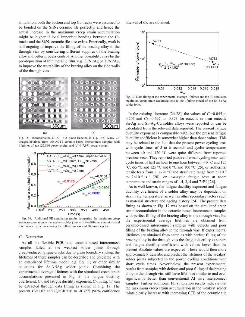
simulation, both the bottom and top Cu tracks were assumed to
be bonded on the Si3N4 ceramic tile perfectly, and hence the
actual increase in the maximum creep strain accumulation
might be higher if local imperfect bonding between the Cu
tracks and the Si3N4 ceramic tile also exists. Practically, work is
still ongoing to improve the filling of the brazing alloy in the
through vias by considering different supplies of the brazing
alloy and better process control. Another possibility may be the
pre-deposition of thin metallic film, e.g. Ti/Ni/Ag or Ti/Ni/Au,
to improve the wettability of the brazing alloy on the side walls
of the through vias.
(a) (b)
Fig. 15. Reconstructed C---C’ Y-Z plane (labeled in Fig. 14b) X-ray CT
images obtained from the ACT1 ceramic-based interconnect samples with
lifetimes of: (a) 125,890 power cycles; and (b) 447,971 power cycles.
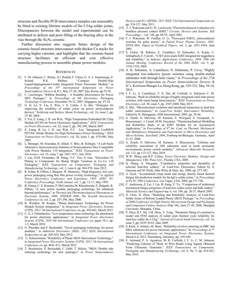
Fig. 16. Additional FE simulation results comparing the maximum creep
strain accumulation in the weakest solder joint with the different ceramic-based
interconnect structures during the reflow process and 50 power cycles.
C. Discussion
As all the flexible PCB, and ceramic-based interconnect
samples failed at the weakest solder joints through
creep-induced fatigue cracks due to grain boundary sliding, the
lifetimes of these samples can be described and predicted with
an established lifetime model. e.g. Eq. (1) or other similar
equations for Sn-3.5Ag solder joints. Combining the
experimental average lifetimes with the simulated creep strain
accumulations presented in Fig. 9, the fatigue ductility
coefficient, C1, and fatigue ductility exponent, C2, in Eq. (1) can
be extracted through data fitting as shown in Fig. 17. The
present C1=1.02 and C2=[-0.516 to -0.327] (90% confidence
interval of C2) are obtained.
Fig. 17. Data fitting of the experimental average lifetimes and the FE simulated
maximum creep strain accumulations to the lifetime model of the Sn-3.5Ag
solder joint.
In the existing literature [24-28], the values of C1=0.045 to
0.205 and C2=-0.697 to -0.323 for eutectic or near eutectic
Sn-Ag and Sn-Ag-Cu solder alloys were reported or can be
calculated from the relevant data reported. The present fatigue
ductility exponent is comparable with, but the present fatigue
ductility coefficient is somewhat higher than those values. This
may be related to the fact that the present power cycling tests
with cycle times of 5 to 6 seconds and cyclic temperatures
between 40 and 120 C were quite different from reported
previous tests. They reported passive thermal cycling tests with
cycle times of half an hour to one hour between -40 °C and 125
°C, -55 °C and 125 °C and 0 °C and 100 °C [25], or isothermal
tensile tests from 11 to 90 °C and strain rate range from 5×10⁻⁵
to 2×10⁻² s−1 [28], or low-cycle fatigue tests at room
temperature and strain ranges of 1.4, 3, 4 and 7.5% [26].
As is well known, the fatigue ductility exponent and fatigue
ductility coefficient of a solder alloy may be dependent on
strain rate, temperature, as well as other secondary factors such
as material structure and ageing history [24]. The present data
fitting as shown in Fig. 17 was based on the simulated creep
strain accumulation in the ceramic-based interconnect samples
with perfect filling of the brazing alloy in the through vias, but
the experimental average lifetimes are obtained from
ceramic-based interconnect samples with defects and poor
filling of the brazing alloy in the through vias. If experimental
lifetimes are obtained from samples with perfect filling of the
brazing alloy in the through vias the fatigue ductility exponent
and fatigue ductility coefficient with values lower than the
present absolute values are expected. These would then more
approximately describe and predict the lifetimes of the weakest
solder joints subjected to the power cycling conditions with
short cycle times. Nevertheless, the present experimental
results from samples with defects and poor filling of the brazing
alloy in the through vias still have lifetimes similar to and even
significantly better than conventional Al wire interconnect
samples. Further additional FE simulation results indicate that
the maximum creep strain accumulation in the weakest solder
joints clearly increase with increasing CTE of the ceramic tile
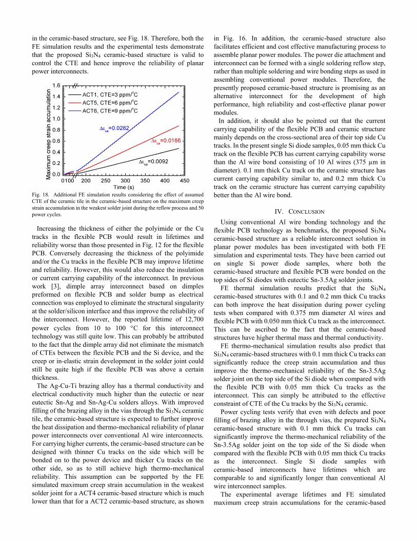
in the ceramic-based structure, see Fig. 18. Therefore, both the
FE simulation results and the experimental tests demonstrate
that the proposed Si3N4 ceramic-based structure is valid to
control the CTE and hence improve the reliability of planar
power interconnects.
Fig. 18. Additional FE simulation results considering the effect of assumed
CTE of the ceramic tile in the ceramic-based structure on the maximum creep
strain accumulation in the weakest solder joint during the reflow process and 50
power cycles.
Increasing the thickness of either the polyimide or the Cu
tracks in the flexible PCB would result in lifetimes and
reliability worse than those presented in Fig. 12 for the flexible
PCB. Conversely decreasing the thickness of the polyimide
and/or the Cu tracks in the flexible PCB may improve lifetime
and reliability. However, this would also reduce the insulation
or current carrying capability of the interconnect. In previous
work [3], dimple array interconnect based on dimples
preformed on flexible PCB and solder bump as electrical
connection was employed to eliminate the structural singularity
at the solder/silicon interface and thus improve the reliability of
the interconnect. However, the reported lifetime of 12,700
power cycles from 10 to 100 C for this interconnect
technology was still quite low. This can probably be attributed
to the fact that the dimple array did not eliminate the mismatch
of CTEs between the flexible PCB and the Si device, and the
creep or in-elastic strain development in the solder joint could
still be quite high if the flexible PCB was above a certain
thickness.
The Ag-Cu-Ti brazing alloy has a thermal conductivity and
electrical conductivity much higher than the eutectic or near
eutectic Sn-Ag and Sn-Ag-Cu solders alloys. With improved
filling of the brazing alloy in the vias through the Si3N4 ceramic
tile, the ceramic-based structure is expected to further improve
the heat dissipation and thermo-mechanical reliability of planar
power interconnects over conventional Al wire interconnects.
For carrying higher currents, the ceramic-based structure can be
designed with thinner Cu tracks on the side which will be
bonded on to the power device and thicker Cu tracks on the
other side, so as to still achieve high thermo-mechanical
reliability. This assumption can be supported by the FE
simulated maximum creep strain accumulation in the weakest
solder joint for a ACT4 ceramic-based structure which is much
lower than that for a ACT2 ceramic-based structure, as shown
in Fig. 16. In addition, the ceramic-based structure also
facilitates efficient and cost effective manufacturing process to
assemble planar power modules. The power die attachment and
interconnect can be formed with a single soldering reflow step,
rather than multiple soldering and wire bonding steps as used in
assembling conventional power modules. Therefore, the
presently proposed ceramic-based structure is promising as an
alternative interconnect for the development of high
performance, high reliability and cost-effective planar power
modules.
In addition, it should also be pointed out that the current
carrying capability of the flexible PCB and ceramic structure
mainly depends on the cross-sectional area of their top side Cu
tracks. In the present single Si diode samples, 0.05 mm thick Cu
track on the flexible PCB has current carrying capability worse
than the Al wire bond consisting of 10 Al wires (375 µm in
diameter). 0.1 mm thick Cu track on the ceramic structure has
current carrying capability similar to, and 0.2 mm thick Cu
track on the ceramic structure has current carrying capability
better than the Al wire bond.
IV. CONCLUSION
Using conventional Al wire bonding technology and the
flexible PCB technology as benchmarks, the proposed Si3N4
ceramic-based structure as a reliable interconnect solution in
planar power modules has been investigated with both FE
simulation and experimental tests. They have been carried out
on single Si power diode samples, where both the
ceramic-based structure and flexible PCB were bonded on the
top sides of Si diodes with eutectic Sn-3.5Ag solder joints.
FE thermal simulation results predict that the Si3N4
ceramic-based structures with 0.1 and 0.2 mm thick Cu tracks
can both improve the heat dissipation during power cycling
tests when compared with 0.375 mm diameter Al wires and
flexible PCB with 0.050 mm thick Cu track as the interconnect.
This can be ascribed to the fact that the ceramic-based
structures have higher thermal mass and thermal conductivity.
FE thermo-mechanical simulation results also predict that
Si3N4 ceramic-based structures with 0.1 mm thick Cu tracks can
significantly reduce the creep strain accumulation and thus
improve the thermo-mechanical reliability of the Sn-3.5Ag
solder joint on the top side of the Si diode when compared with
the flexible PCB with 0.05 mm thick Cu tracks as the
interconnect. This can simply be attributed to the effective
constraint of CTE of the Cu tracks by the Si3N4 ceramic.
Power cycling tests verify that even with defects and poor
filling of brazing alloy in the through vias, the prepared Si3N4
ceramic-based structure with 0.1 mm thick Cu tracks can
significantly improve the thermo-mechanical reliability of the
Sn-3.5Ag solder joint on the top side of the Si diode when
compared with the flexible PCB with 0.05 mm thick Cu tracks
as the interconnect. Single Si diode samples with
ceramic-based interconnects have lifetimes which are
comparable to and significantly longer than conventional Al
wire interconnect samples.
The experimental average lifetimes and FE simulated
maximum creep strain accumulations for the ceramic-based
structure and flexible PCB interconnect samples can reasonably
be fitted to existing lifetime models of Sn-3.5Ag solder joints,
Discrepancies between the model and experimental can be
attributed to defects and poor filling of the brazing alloy in the
vias through the Si3N4 ceramic.
Further discussion also suggests future design of the
ceramic-based structure interconnect with thicker Cu tracks for
carrying higher currents, and highlights that the ceramic-based
structure facilitates an efficient and cost effective
manufacturing process to assemble planar power modules.
REFERENCES
[1] C .M. Johnson, C. Buttay, S.J. Rashid, F. Udrea, G. A .J. Amaratunga, P.
Ireland, R.K. Malhan, “Compact Double-Side
Liquid-Impingement-Cooled Integrated Power Electronic Module,” in Proceedings of the 19th International Symposium on Power
Semiconductor Devices & ICs, May 27-30, 2007 Jeju, Korea, pp.53-56.
[2] C. Luechinger, “Ribbon Bonding – A Scalable Interconnect for Power
QFN Packages,” in Proceedings of 9th Electronics Packaging
Technology Conference, December 10-12, 2007, Singapore, pp. 47-54.
[3] G. Q. Lu, X. Liu, S. Wen, J. N. Calata, J. G. Bai, “Strategies for improving the reliability of solder joints on power semiconductor
devices,” Soldering and Surface Mount Technology, vol. 16, issue 2, pp.
27-40, 2004.. [4] J. Yin, Z. Liang, J. D. van Wyk, “High Temperature Embedded SiC Chip
Module (ECM) for Power Electronics Applications,” IEEE Transactions
on Power Electronics, vol. 22, issue 2, pp. 392-398, March 2007. [5] Z. Liang, B. Lu, J. D. van Wyk, F.C . Lee, “Integrated CoolMOS
FET/SiC-Diode Module for High Performance Power Switching,” IEEE
Transactions on Power Electronics, vol. 20, issue 3, pp. 679-686, May 2005.
[6] L. Menager, M. Soueidan, B. Allard, V. Bley, B. Schlegel, “A Lab-Scale
Alternative Interconnection Solution of Semiconductor Dice Compatible with Power Modules 3-D Integration,” IEEE Transactions on Power
Electronics, vol. 25, issue 7, pp. 1667-1671, July 2010.
[7] J. Lee, D.M. Fernandez, M. Paing, Y.C. Yeo, S. Gao, “Electroless Ni
Plating to Compensate for Bump Height Variation in Cu–Cu 3-D
Packaging,” IEEE Transactions on Components, Packaging and Manufacturing Technology, vol. 2, issue 6, pp. 964-970, June 2012.
[8] R. Fisher, R. Fillion, J. Burgess, W. Hennessy, "High frequency, low cost,
power packaging using thin film power overlay technology," in Applied Power Electronics Conference and Exposition, 1995. APEC '95.
Conference Proceedings, Tenth Annual, vol. 1, pp. 12-17, May 1995.
[9] B. Ozmat, C. S. Korman, P. McConnelee,M. Kheraluwala, E. Delgado, R. Pillion, "A new power module packaging technology for enhanced
thermal performance," in Thermal and Thermomechanical Phenomena in
Electronic Systems, 2000. ITHERM 2000. The Seventh Intersociety Conference on, vol. 2, pp. 287-296, May 2000.
[10] K. Weidner, M. Kaspar, "Planar Interconnect Technology for Power
Module System Integration," in Integrated Power Electronics Systems (CIPS), 2012 7th International Conference on, pp. 459-463, March 2012.
[11] C. G, J. Faltenbacher, "Low temperature sinter technology die attachment
for power electronic applications," in Integrated Power Electronics Systems (CIPS), 2010 6th International Conference on, paper 10.1, pp.
1-5, March 2010.
[12] N. Pluschke and P. Beckedahl, "Novel packaging technology for power modules," in Industrial Electronics (ISIE), 2012 IEEE International
Symposium on, pp. 420-424, May 2012.
[13] U. Scheuermann, "Reliability of Planar SKiN Interconnect Technology," in Integrated Power Electronics Systems (CIPS), 2012 7th International
Conference on, pp. 4641-471, March 2012.
[14] T. Stockmeier, P. Beckedahl, C. Göbl, T. Malzer, "SKiN: Double side sintering technology for new packages," in Power Semiconductor
Devices and ICs (ISPSD), 2011 IEEE 23rd International Symposium on,
pp. 324-327, May 2011. [15] F. J. Wakeman and G. W. Lockwood, "Electromechanical evaluation of a
bondless pressure contact IGBT," Circuits, Devices and Systems, IEE
Proceedings -, vol. 148, pp. 89-93, April 2001. [16] F. J. Wakeman, W. Findlay, G. Li, "Press-pack IGBTs, semiconductor
switches for pulse power," in Pulsed Power Plasma Science, 2001.
PPPS-2001. Digest of Technical Papers, vol. 2, pp. 1051-1054, June 2001.
[17] S. Eicher, M. Rahimo, E. Tsyplakov, D. Schneider, A. Kopta, U.
Schlapbach, E. Carroll., "4.5kV press pack IGBT designed for ruggedness and reliability," in Industry Applications Conference, 2004. 39th IAS
Annual Meeting. Conference Record of the 2004 IEEE, vol. 3, pp.
1534-1539, 2004.
[18] A. K. Solomon, A. Castellazzi, N. Delmonte, P. Cova, “Highly
integrated low-inductive power switches using double-etched
substrates with through-hole viases,” in Proceedings of the 27th
International Symposium on Power Semiconductor Devices &
IC's, Kowloon Shangri-La, Hong Kong, pp. 329-332, May 10-14,
2015. [19] J. F. Li, A. Castellazzi, T. X. Dai, M. Corfield, A. Solomon, C. M.
Johnson, “Built-in reliability design of highly integrated solid-state power
switches with metal bump interconnects,” IEEE Transactions on Power
Electronics, vol. 30, issue 5, pp. 2587-2600, May 2015. [20] Z. Mei, “Microstructual evolution and interfacial interaction in lead-free
solder interconnects,” in Lead-Free Solder Interconnect Reliability,
Edited by D. Shangguan, ASM International, 2005, pp. 29-66. [21] A. Zéanh, O. Dalverny, M. Karama, E. Woirgard, S. Azzopardi, A.
Bouzourene1, J. Casutt, M.M. Guyennet, “Thermomechanical Modelling
and Reliability Study of an IGBT Module for an Aeronautical Application,” in Proceedings of 9th Int. Conf. on Thermal, Mechanical
and Multiphysics Simulation and Experiments in Micro-Electronics and
Micro-Systems, EuroSimE 2008, Freiburg-im-Breisgau, Germany, April 21-23, 2008.
[22] A. Zeanh, O. Dalverny, M. Karama, A. Bouzourene, “Lifetime and
reliability assessment of AlN substrates used in harsh aeronautic environments power switch modules,” Advanced Materials Research,
vol. 112, pp 113-127, May 2010.
[23] W.W. Sheng and R.P. Colino, Power Electronic Modules: Design and Manufacture, CRC Press LLC, Florida, USA, 2005.
[24] Q. Zhang, A. Dasgupta, “Constitutive properties and durability of
selected lead-free solders,” in Leed-Free Electronics, Edited by S. Ganesan and M. Pecht, John Wiley & Sons, Inc, 2006, pp. 237-382.
[25] A. Syed, “Accumulated creep strain and energy density based thermal
fatigue life prediction models for SnAgCu solder joints,” in Proceedings of ECTC 2004 Conference, Las Vegas, USA, 2004, pp.737-746.
[26] C. Andersson, Z. Lai, J. Liu, H. Jiang, Y. Yu, “Comparison of isothermal
mechanical fatigue properties of lead-free solder joints and bulk solders,” Materials Science and Engineering A, vol. 394, pp. 20-27, March 2005.
[27] X. Chen, D. Zhou, “Modeling and Reliability Analysis of Lead-Free
Solder Joints of Bottom Leaded Plastic (BLP) Package,” in Proceedings of 2006 Conference on High Density Microsystem Design and Packaging
and Component Failure Analysis (Hdp '06), June 27-30, 2006, Shanghai University, Shanghai, China.
[28] P. Zhou, B.T. Hu, J.M. Zhou, Y. Yang, “Parameter fitting of constitutive
model and FEM analysis of solder joint thermal cycle reliability for lead-free solder Sn-3.5Ag,” Journal of Central South University, vol. 16,
issue 3, pp. 0339−0343, June 2009.
[29] S. Kraft, A. Schletz, M. Marz, “Reliability of silver sintering on DBC and DBA substrates for power electronic applications,” In: Proceedings of 7th
International Conference on Integrated Power Electronics Systems,
March 6-8, 2012, Nuremberg, Germany, pp. 439-444. [30] E. Arjmand, P. A. Agyakwa, M. R. Corfield, J. F. Li, C. M. Johnson,
“Predicting Lifetime of Thick Al Wire Bonds Using Signals Obtained
From Ultrasonic Generator,” IEEE Transactions on Components, Packaging and Manufacturing Technology, vol. 6, No. 5, pp. 814-821,
May 2016.
Recommended