Embed Size (px)
Citation preview

8086 in minimum mode
Sridari Iyer
St. Francis Inst. of Tech
Borivali (W), Mumbai

Minimum Mode
•Single Processor Mode
•The Processor is in control of all the three buses – address, data and control.

Multiplexed Pins
• Multiplexed pins perform different functions at different time intervals
• These functions will never be required by the μp or its peripherals simultaneously.
• E.g., Address and Data pins are multiplexed.
• The μp first sends out address, and then from that location/ to that location, the μp sends/ receives data.
• Same pins act as address lines in one time state (T1), and data lines in another time state (T3)

Time in μP
• T-state is the smallest unit of time in a μp
•1 clock cycle = 1 T-state
• In 8086, 1 machine cycle = 4 T-states
• 1 machine cycle (or bus cycle) is the time required to
• T1 – send out an address – on address bus
• T2 – send out a signal (read/ write) – on control bus
• T3 – read/ write data on that location – on data bus
• T4 – release all buses
• 1 instruction cycle = nmachine cycles
(depends on the instruction)

What is a “BUS” in real?
• Bus is a way of transport
• Are these pins or electrical wires?

• The 8086 ALU sets the pins A0 – A19 to match the 20-bit address of the location it wants to access
• This value is not stored on these pins for a long time
• This value gets rewritten as D0 – D15 and status lines within the next fraction of a second
• Where is A0 – A19 after that?
• In the address bus!
• How to get pure address from AD0 – AD15? (Demultiplex)
By using a LATCH
to save only the address from these pins,
and remain cut-off when data is on them.
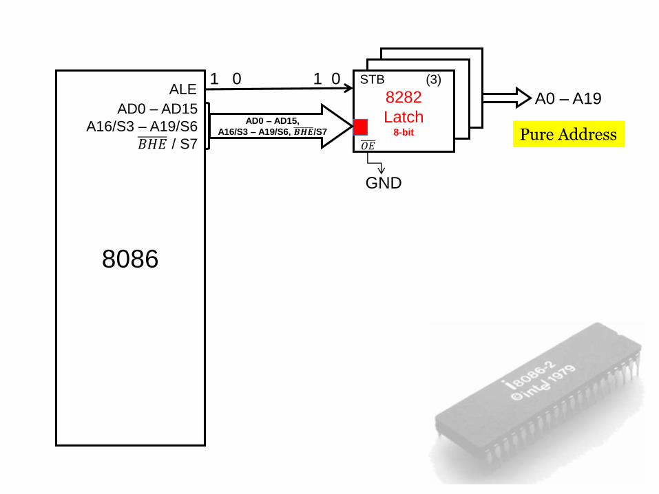
8086
80868086STB (3)
8282
Latch8-bit
ALE
AD0 – AD15
A16/S3 – A19/S6
𝐵𝐻𝐸 / S7
1
GND
A0 – A19
𝑂𝐸
010
AD0 – AD15,
A16/S3 – A19/S6, 𝑩𝑯𝑬/S7 Pure Address

8086
80868086STB (3)
8282
Latch8-bit
ALE
AD0 – AD15
A16/S3 – A19/S6
𝐵𝐻𝐸 / S7
AD0 – AD15,
A16/S3 – A19/S6, 𝑩𝑯𝑬/S7
1
GND
A0 – A19
𝑂𝐸
D0 – D158086(2)
8286
Transreciever8-bit
𝑂𝐸
TDT/ 𝑅
𝐷𝐸𝑁
AD
0 –
AD
15
Pure Data

8086
80868086STB (3)
8282
Latch8-bit
ALE
AD0 – AD15
A16/S3 – A19/S6
𝑩𝑯𝑬 / S7
AD0 – AD15,
A16/S3 – A19/S6, 𝑩𝑯𝑬/S7
1
GND
A0 – A19
𝑂𝐸
D0 – D158086(2)
8286
Transreciever8-bit
𝑂𝐸
TDT/ 𝑹
𝑫𝑬𝑵
AD
0 –
AD
15
74138
3:8
Decoder
C
B
A
Y0
Y1
Y2
Y3
Y4
Y5
Y6
Y7
M/𝑰𝑶
𝑹𝑫
𝑾𝑹
IORIOW
MEMRMEMW
0 0 1 1IOR IOW MR MW
0 1 0 1
1 0 1 0
Control Signals
Address Bus
Data Bus
Control Bus

8086
at
6MHz
80868086STB (3)
8282
Latch8-bit
ALE
AD0 – AD15
A16/S3 – A19/S6
𝑩𝑯𝑬 / S7
AD0 – AD15,
A16/S3 – A19/S6, 𝑩𝑯𝑬 / S
1
GND
A0 – A19
𝑂𝐸
D0 – D15
8086(2)
8286
Transreciever8-bit
𝑂𝐸
TDT/ 𝑹
𝑫𝑬𝑵A
D0
–A
D15
74138
3:8
Decoder
C
B
A
Y0
Y1
Y2
Y3
Y4
Y5
Y6
Y7
M/𝑰𝑶
𝑹𝑫
𝑾𝑹
IORIOW
MEMRMEMW
0 0 1 1IOR IOW MR MW
0 1 0 1
1 0 1 0
Control Signals
8284Clock
18 MHz
CLK
READY
RESET
CLK
RESET
RDY

8086
at
6MHz
80868086STB (3)
8282
Latch8-bit
ALE
AD0 – AD15
A16/S3 – A19/S6
𝑩𝑯𝑬 / S7
AD0 – AD15,
A16/S3 – A19/S6, 𝑩𝑯𝑬/ S7
1
GND
A0 – A19
𝑂𝐸
D0 – D15
8086(2)
8286
Transreciever8-bit
𝑂𝐸
TDT/ 𝑹
𝑫𝑬𝑵A
D0
–A
D15
74138
3:8
Decoder
C
B
A
Y0
Y1
Y2
Y3
Y4
Y5
Y6
Y7
M/𝑰𝑶
𝑹𝑫
𝑾𝑹
IORIOW
MEMRMEMW
0 0 1 1IOR IOW MR MW
0 1 0 1
1 0 1 0
Control Signals
8284Clock
18 MHz
CLK
READY
RESET
CLK
RESET
RDY
MN/𝑴𝑿Vcc
NMI
INTA
INTR
HLDA
HOLD
Interrupts
DMAC
𝑻𝑬𝑺𝑻

8086
at
6MHz
80868086
STB
(3)
8282
Latch8-bit
ALE
AD0 – AD15
A16/S3 – A19/S6
𝑩𝑯𝑬 / S7
AD0 – AD15,
A16/S3 – A19/S6, 𝑩𝑯𝑬 / S7
1
GND
A0 – A19
𝑂𝐸
D0 – D15
8086(2)
8286
Transreciever8-bit
𝑂𝐸
TDT/ 𝑹
𝑫𝑬𝑵
AD
0 –
AD
15
74138
3:8
Decoder
C
B
A
Y0
Y1
Y2
Y3
Y4
Y5
Y6
Y7
M/𝑰𝑶
𝑹𝑫
𝑾𝑹
IORIOW
MEMR
MEMW
0 0 1 1
IOR IOW MR MW
0 1 0 1
1 0 1 0
Control Signals
8284Clock
18 MHz
CLK
READY
RESET
CLK
RESET
RDY
MN/𝑴𝑿Vcc
NMI
INTA
INTR
HLDA
HOLD
Interrupts
DMAC
𝑻𝑬𝑺𝑻
8086 in Minimum Mode!


![[HITB Amsterdam 2010]Breaking Virtualization By Switching To Virtual 8086 Mode Final](https://img.pdfslide.net/doc/110x75/5584c664d8b42aeb138b48a2/hitb-amsterdam-2010breaking-virtualization-by-switching-to-virtual-8086-mode-final.jpg)