Embed Size (px)
Citation preview
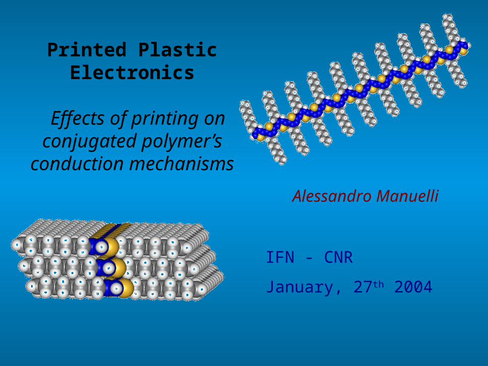
Printed Plastic Electronics
Effects of printing on conjugated polymer’s
conduction mechanisms
IFN - CNR
January, 27th 2004
Alessandro Manuelli
© Manuelli 2005
2/52
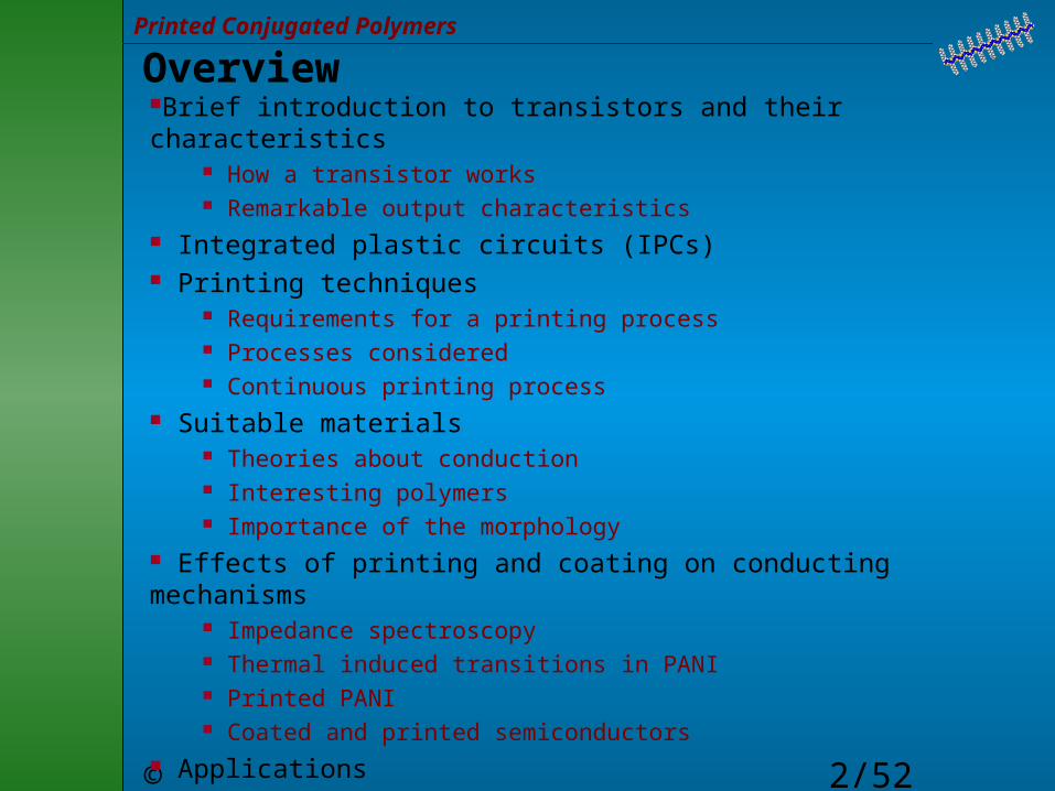
Printed Conjugated Polymers
OverviewBrief introduction to transistors and their characteristics
How a transistor works Remarkable output characteristics
Integrated plastic circuits (IPCs) Printing techniques
Requirements for a printing process Processes considered Continuous printing process
Suitable materials Theories about conduction Interesting polymers Importance of the morphology
Effects of printing and coating on conducting mechanisms Impedance spectroscopy Thermal induced transitions in PANI Printed PANI Coated and printed semiconductors
Applications Outlook
© Manuelli 2005
3/52
Printed Conjugated Polymers
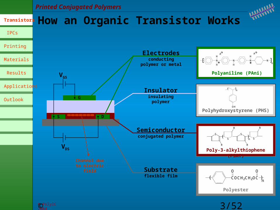
How an Organic Transistor WorksTransistors
IPCs
Printing
Materials
Results
Applications
Outlook
© PolyIC 2004
S D
G
NNN N
H H
H H
[ ]no+o+
o- o-AA
Polyaniline (PAni)
Electrodesconducting polymer
or metal
OH
( )n
Polyhydroxystyrene (PHS)
Insulatorinsulating polymer
n)(
S
R
S
R
S
R
S
R
Poly-3-alkylthiophene (P3AT)
Semiconductorconjugated polymer
COCH2CH2OC
O O
n)(
Polyester
Substrateflexible film
VGS
VDS
Channel due to electric field
© Manuelli 2005
4/52
Printed Conjugated Polymers
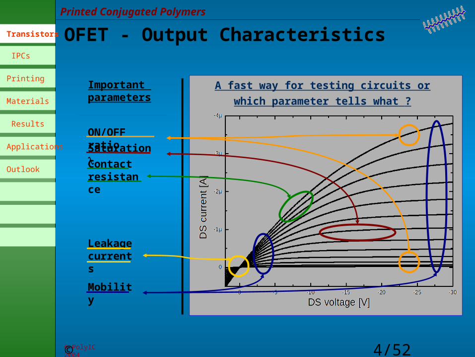
OFET - Output Characteristics
© PolyIC 2004
Saturation
Important parameters
Contact resistance
Mobility
Leakage currents
ON/OFF ratio
A fast way for testing circuits orwhich parameter tells what ?
Transistors
IPCs
Printing
Materials
Results
Applications
Outlook
© Manuelli 2005
5/52
Printed Conjugated Polymers
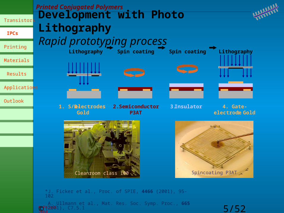
Spin coating
2. SemiconductorP3AT
Spin coating
3. Insulator
Lithography
4. Gate-electrode: Gold
:
Lithography
1. S/D-electrodesGold
Cleanroom class 100 Spincoating P3AT
*J. Ficker et al., Proc. of SPIE, 4466 (2001), 95-102 A. Ullmann et al., Mat. Res. Soc. Symp. Proc., 665 (2001), C7.5.1
Development with Photo Lithography Rapid prototyping process
© PolyIC 2004
Transistors
IPCs
Printing
Materials
Results
Applications
Outlook
© Manuelli 2005
6/52
Printed Conjugated Polymers
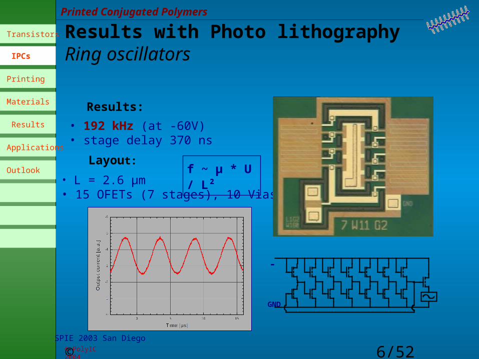
SPIE 2003 San Diego
GND
-
• 192 kHz (at -60V)• stage delay 370 ns
• L = 2.6 µm• 15 OFETs (7 stages), 10 Vias
Layout:
Results:
f ~ µ * U / L²
© PolyIC 2004
Results with Photo lithographyRing oscillators
Transistors
IPCs
Printing
Materials
Results
Applications
Outlook
© Manuelli 2005
7/52
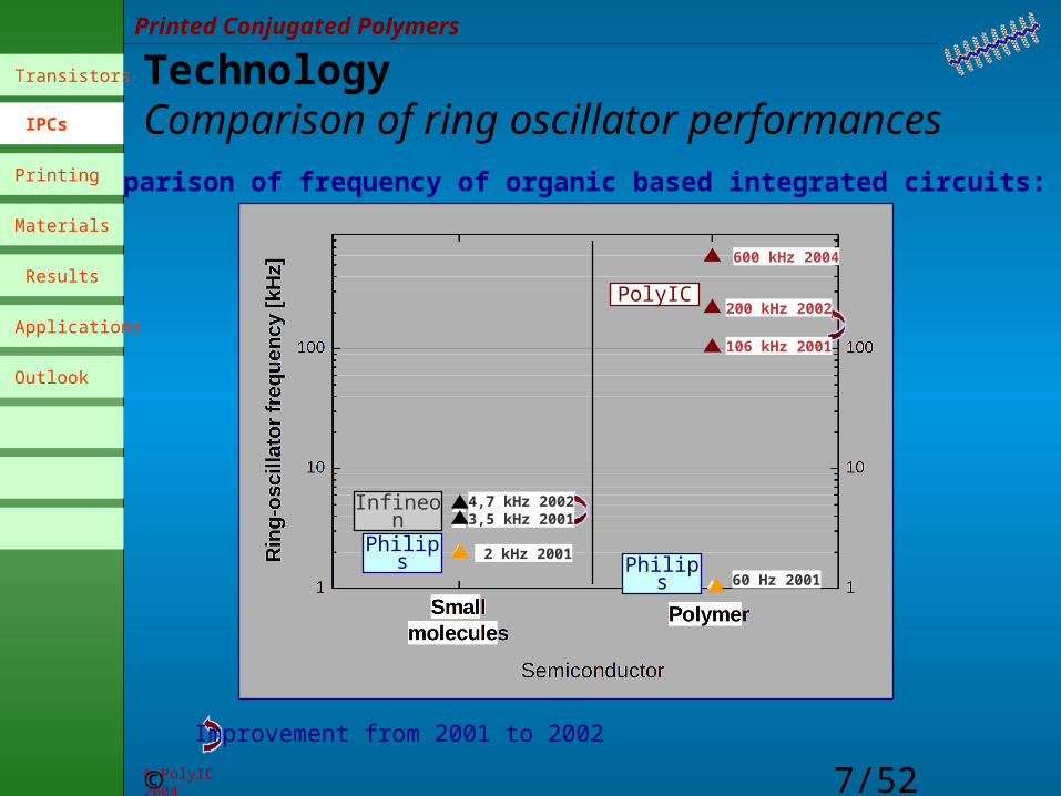
Printed Conjugated Polymers
Comparison of frequency of organic based integrated circuits:
Improvement from 2001 to 2002© PolyIC 2004
TechnologyComparison of ring oscillator performances
Infineon 4,7 kHz 20023,5 kHz 2001
PhilipsPhilips 2 kHz 2001
60 Hz 2001
PolyIC200 kHz 2002
106 kHz 2001
600 kHz 2004
Transistors
IPCs
Printing
Materials
Results
Applications
Outlook
© Manuelli 2005
8/52
Printed Conjugated Polymers
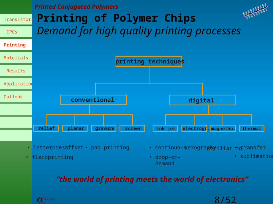
conventional digital
relief planar gravure screen ink jet electrogr. thermalmagnetho.
• letterpress
• flexoprinting
• offset • pad printing • continuous
• drop-on- demand
• xerography similiar to • transfer
• sublimation
printing techniques
“the world of printing meets the world of electronics”
© PolyIC 2004
Printing of Polymer ChipsDemand for high quality printing processes
Transistors
IPCs
Printing
Materials
Results
Applications
Outlook
© Manuelli 2005
9/52
Printed Conjugated Polymers
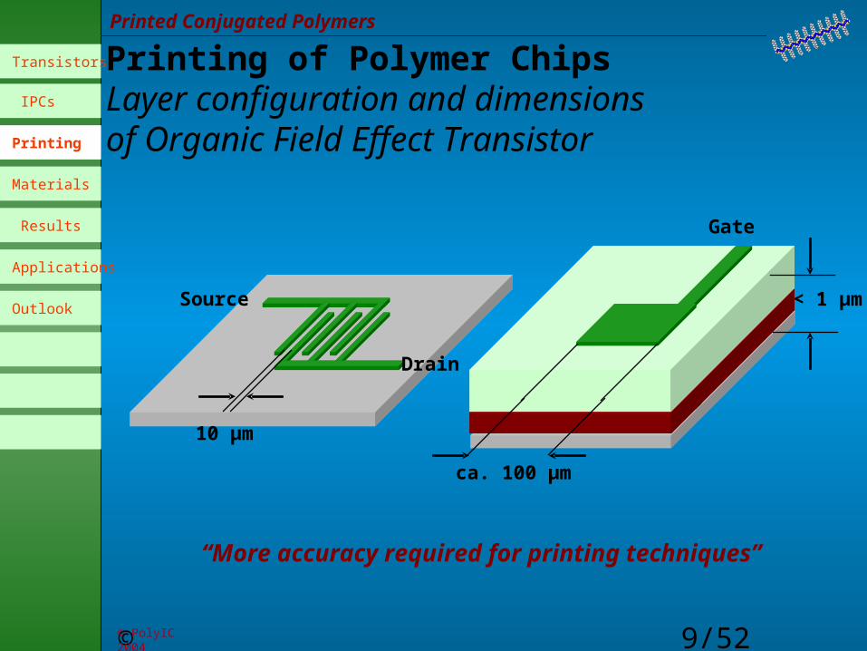
< 1 µm
Printing of Polymer ChipsLayer configuration and dimensionsof Organic Field Effect Transistor
10 µm
Drain
Source
ca. 100 µm
Gate
“More accuracy required for printing techniques”
© PolyIC 2004
Transistors
IPCs
Printing
Materials
Results
Applications
Outlook
© Manuelli 2005
10/52
Printed Conjugated Polymers
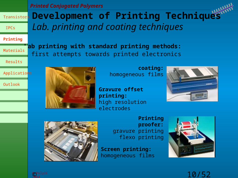
Lab printing with standard printing methods:• first attempts towards printed electronics
Gravure offset printing:high resolution electrodes
Screen printing:homogeneous films
Printing proofer:gravure printing
flexo printing
coating:homogeneous films
© PolyIC 2004
Development of Printing TechniquesLab. printing and coating techniques
Transistors
IPCs
Printing
Materials
Results
Applications
Outlook
© Manuelli 2005
11/52
Printed Conjugated Polymers
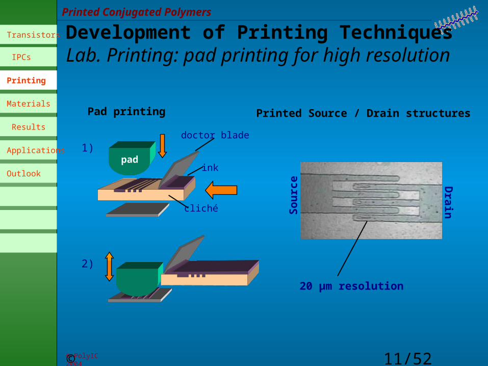
cliché
pad
doctor blade
ink
20 µm resolution
Pad printing Printed Source / Drain structures
1)
2)
Sour
ce Drain
© PolyIC 2004
Development of Printing TechniquesLab. Printing: pad printing for high resolution
Transistors
IPCs
Printing
Materials
Results
Applications
Outlook
© Manuelli 2005
12/52
Printed Conjugated Polymers
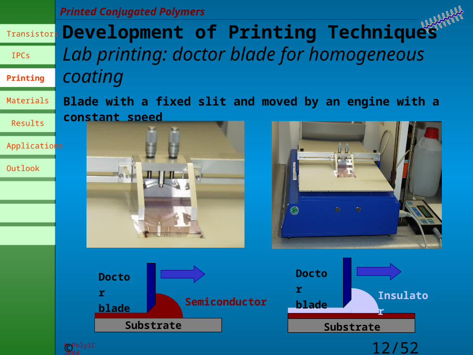
Blade with a fixed slit and moved by an engine with a constant speed
Substrate
Semiconductor
Doctor blade Insulator
Substrate
Doctor blade
Development of Printing Techniques Lab printing: doctor blade for homogeneous coating
© PolyIC 2004
Transistors
IPCs
Printing
Materials
Results
Applications
Outlook
© Manuelli 2005
13/52
Printed Conjugated Polymers
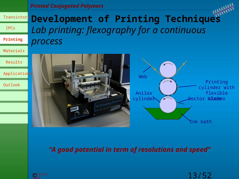
Development of Printing Techniques Lab printing: flexography for a continuous process
“A good potential in term of resolutions and speed”
Ink bath
Anilox cylinder Doctor blade
Printing cylinder with flexible stereo
Web
© PolyIC 2004
Transistors
IPCs
Printing
Materials
Results
Applications
Outlook
© Manuelli 2005
14/52
Printed Conjugated Polymers
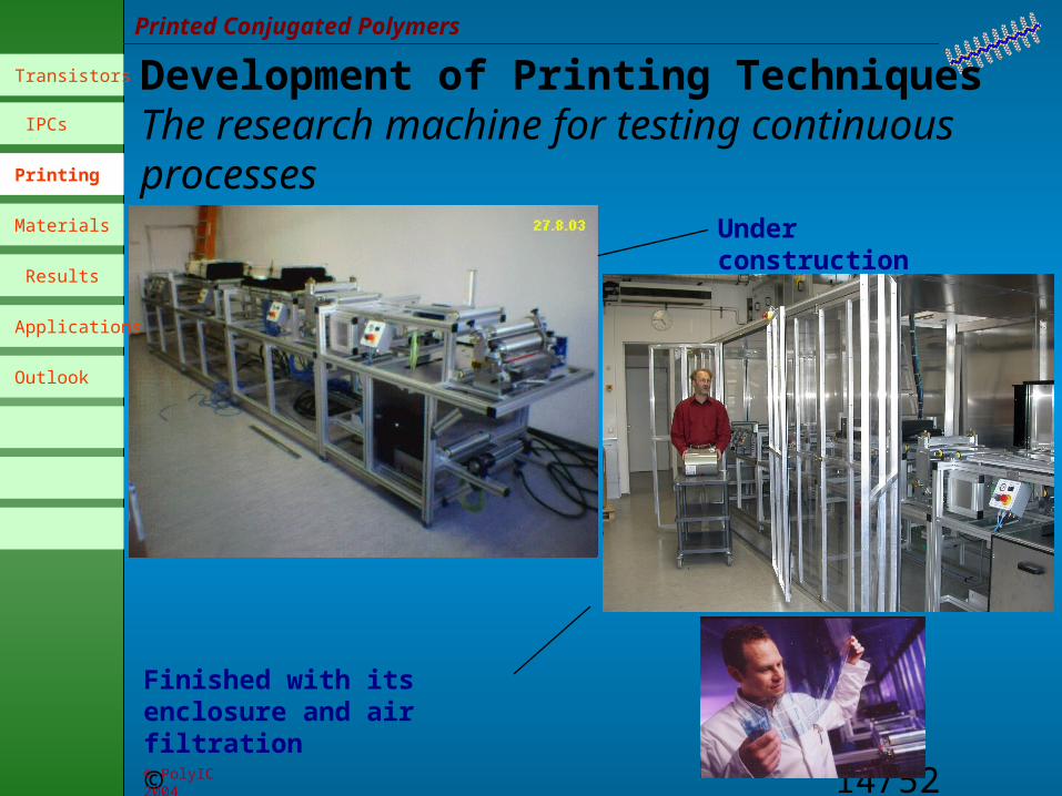
Development of Printing TechniquesThe research machine for testing continuous processes
Under construction
Finished with its enclosure and air filtration
© PolyIC 2004
Transistors
IPCs
Printing
Materials
Results
Applications
Outlook
© Manuelli 2005
15/52
Printed Conjugated Polymers
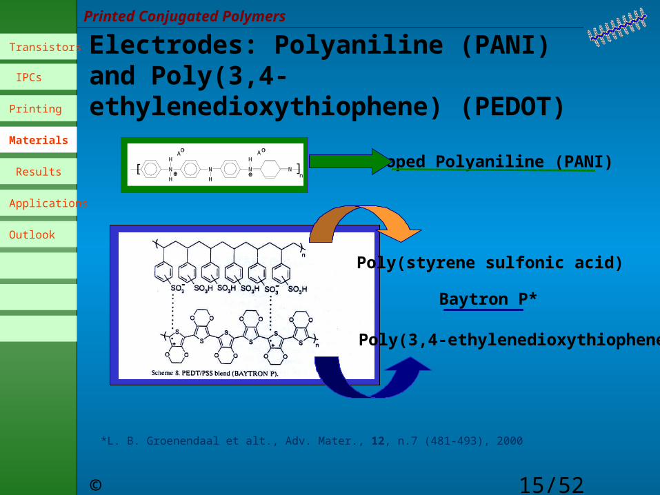
Electrodes: Polyaniline (PANI) and Poly(3,4-ethylenedioxythiophene) (PEDOT)
NNN N
H H
H H
[ ]no+o+
o- o-AA
Doped Polyaniline (PANI)
Poly(styrene sulfonic acid)
Poly(3,4-ethylenedioxythiophene)
Baytron P*
*L. B. Groenendaal et alt., Adv. Mater., 12, n.7 (481-493), 2000
Transistors
IPCs
Printing
Materials
Results
Applications
Outlook
© Manuelli 2005
16/52
Printed Conjugated Polymers
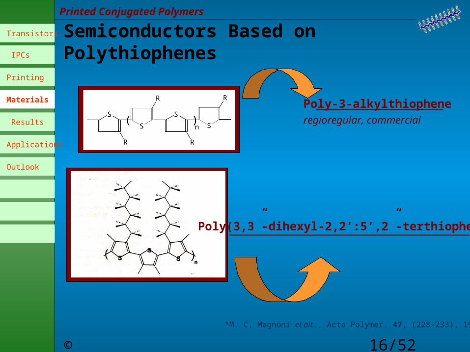
Semiconductors Based on Polythiophenes
n)(
S
R
S
R
S
R
S
R Poly-3-alkylthiophene regioregular, commercial
*M. C. Magnoni et alt., Acta Polymer. 47, (228-233), 1996
Poly(3,3”-dihexyl-2,2’:5’,2”-terthiophene)*
Transistors
IPCs
Printing
Materials
Results
Applications
Outlook
© Manuelli 2005
17/52
Printed Conjugated Polymers
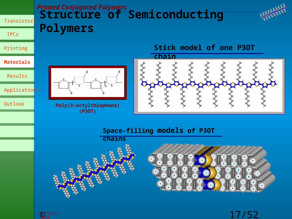
Structure of Semiconducting Polymers
Space-filling models of P3OT chains
Stick model of one P3OT chain
Poly(3-octylthiophene) (P3OT)
n)(
S
R
S
R
S
R
S
R
© PolyIC 2004
Transistors
IPCs
Printing
Materials
Results
Applications
Outlook
© Manuelli 2005
18/52
Printed Conjugated Polymers
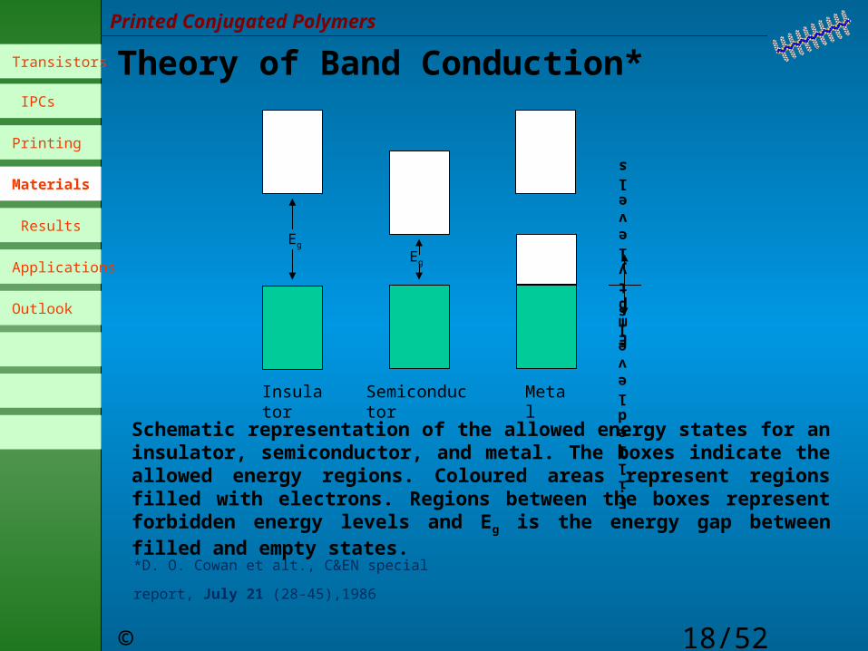
Theory of Band Conduction*
*D. O. Cowan et alt., C&EN special report, July 21
(28-45),1986
Eg
Eg Empty levels
Filled levels
Insulator Semiconductor Metal
Schematic representation of the allowed energy states for an insulator, semiconductor, and metal. The boxes indicate the allowed energy regions. Coloured areas represent regions filled with electrons. Regions between the boxes represent forbidden energy levels and Eg is the energy gap between filled and empty states.
Transistors
IPCs
Printing
Materials
Results
Applications
Outlook
© Manuelli 2005
19/52
Printed Conjugated Polymers
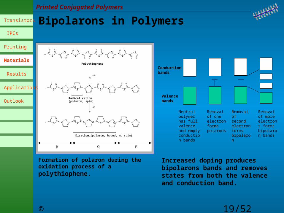
Bipolarons in Polymers
Dication (bipolaron, bound, no spin)
Radical cation(polaron, spin)
SS
SS
SS
SS
-e-
SS
SS
SS
SS
-e-
SS
SS
SS
SS
Polythiophene
QB B
Formation of polaron during the oxidation process of a polythiophene.
Conduction bands
Valence bands
Neutral polymer has full valence and empty conduction bands
Removal of one electron forms polarons
Removal of second electron forms bipolaron
Removal of more electrons forms bipolaron bands
Increased doping produces bipolarons bands and removes states from both the valence and conduction band.
Transistors
IPCs
Printing
Materials
Results
Applications
Outlook
© Manuelli 2006
20/52
Printed Conjugated Polymers
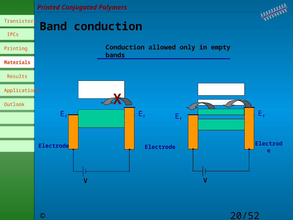
Band conduction
X
Conduction allowed only in empty bands
Ef Ef EfEf
V V
Electrode Electrode Electrode
Transistors
IPCs
Printing
Materials
Results
Applications
Outlook
© Manuelli 2005
21/52
Printed Conjugated Polymers
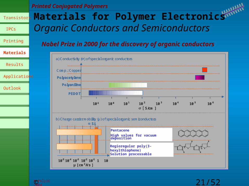
Materials for Polymer ElectronicsOrganic Conductors and Semiconductors
Nobel Prize in 2000 for the discovery of organic conductors
regioregular Poly(3-hexylthiophen)solution processable
Pentacenhigh values for vacuum deposition
10-5 10-4 10-3 10-2 10-1 1 10µ [ cm2/Vs ]
-
Si
S/cm ]10 510 410 310 210 110 010-1 10 6
Comp.: Copper
Polyacetylene
Polyaniline
PEDOT
b) Charge carrier mobility (µ) of special organic semiconductors
a) Conductivity () of special organic conductors
n)(
S
R
S
R
S
R
S
R
PentaceneHigh values for vacuum deposition
Regioregular poly(3-hexylthiophene)Solution processable
© PolyIC 2004
Transistors
IPCs
Printing
Materials
Results
Applications
Outlook
© Manuelli 2005
22/52
Printed Conjugated Polymers
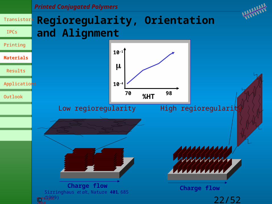
Regioregularity, Orientation and Alignment
Sirringhaus et alt., Nature 401, 685 (1999) Charge flow
SS
SS
SS
SS
Low regioregularity High regioregularity
Charge flow
S S
S S
SS
SS
10-1
10-4
70 98%HT
© PolyIC 2004
Transistors
IPCs
Printing
Materials
Results
Applications
Outlook
© Manuelli 2005
23/52
Printed Conjugated Polymers
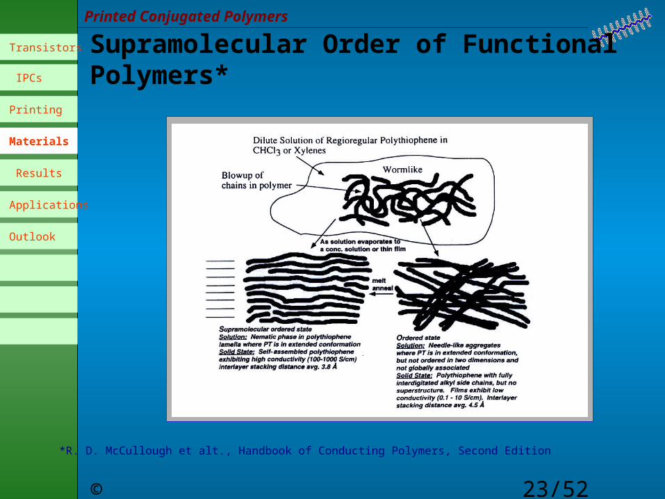
Supramolecular Order of Functional Polymers*
*R. D. McCullough et alt., Handbook of Conducting Polymers, Second Edition
Transistors
IPCs
Printing
Materials
Results
Applications
Outlook
© Manuelli 2005
24/52
Printed Conjugated Polymers
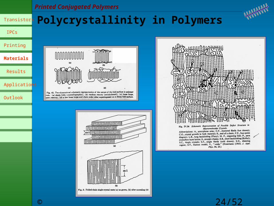
Polycrystallinity in PolymersTransistors
IPCs
Printing
Materials
Results
Applications
Outlook
© Manuelli 2005
25/52
Printed Conjugated Polymers
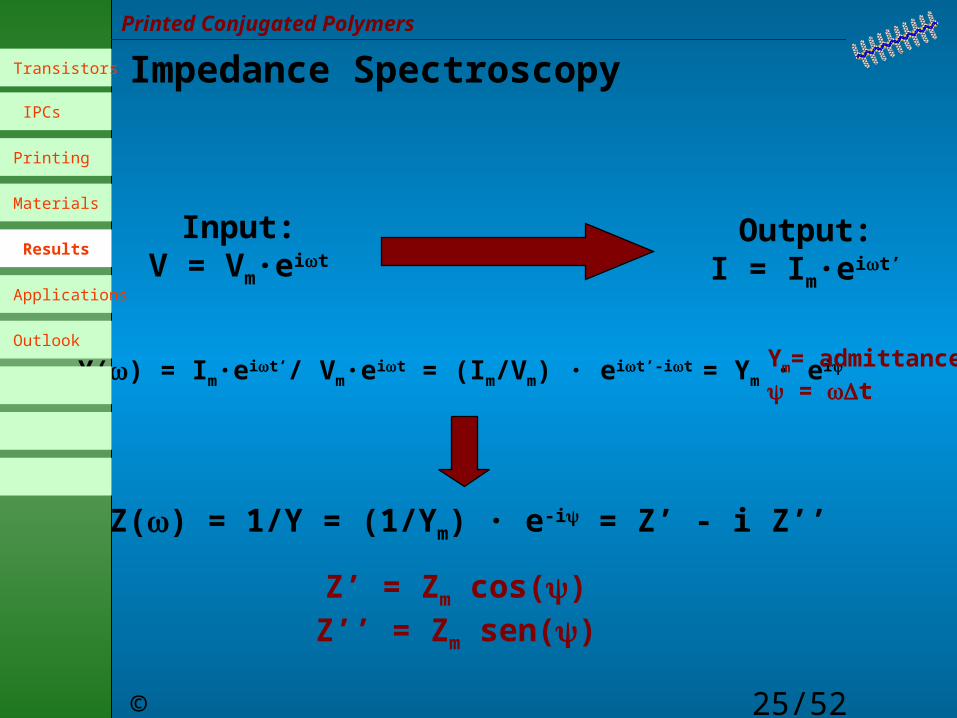
Impedance Spectroscopy
Input:V = Vm·eit
Output:I = Im·eit’
Y() = Im·eit’/ Vm·eit = (Im/Vm) · eit’-it = Ym · ei Ym= admittance = t
Z() = 1/Y = (1/Ym) · e-i = Z’ - i Z’’
Z’ = Zm cos()Z’’ = Zm sen()
Transistors
IPCs
Printing
Materials
Results
Applications
Outlook
© Manuelli 2005
26/52
Printed Conjugated Polymers
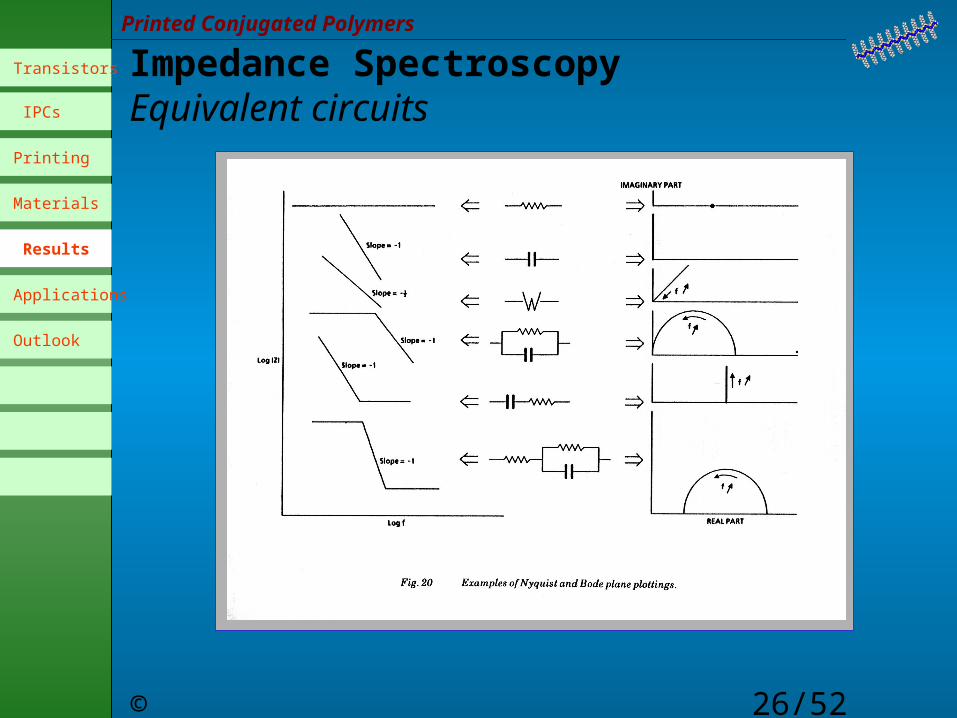
Impedance SpectroscopyEquivalent circuits
Transistors
IPCs
Printing
Materials
Results
Applications
Outlook
© Manuelli 2005
27/52
Printed Conjugated Polymers
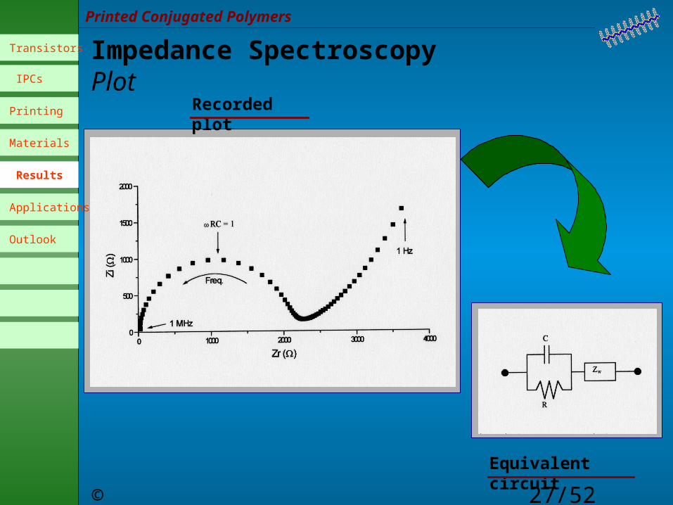
Impedance SpectroscopyPlot
Recorded plot
Equivalent circuit
Transistors
IPCs
Printing
Materials
Results
Applications
Outlook
© Manuelli 2005
28/52
Printed Conjugated Polymers
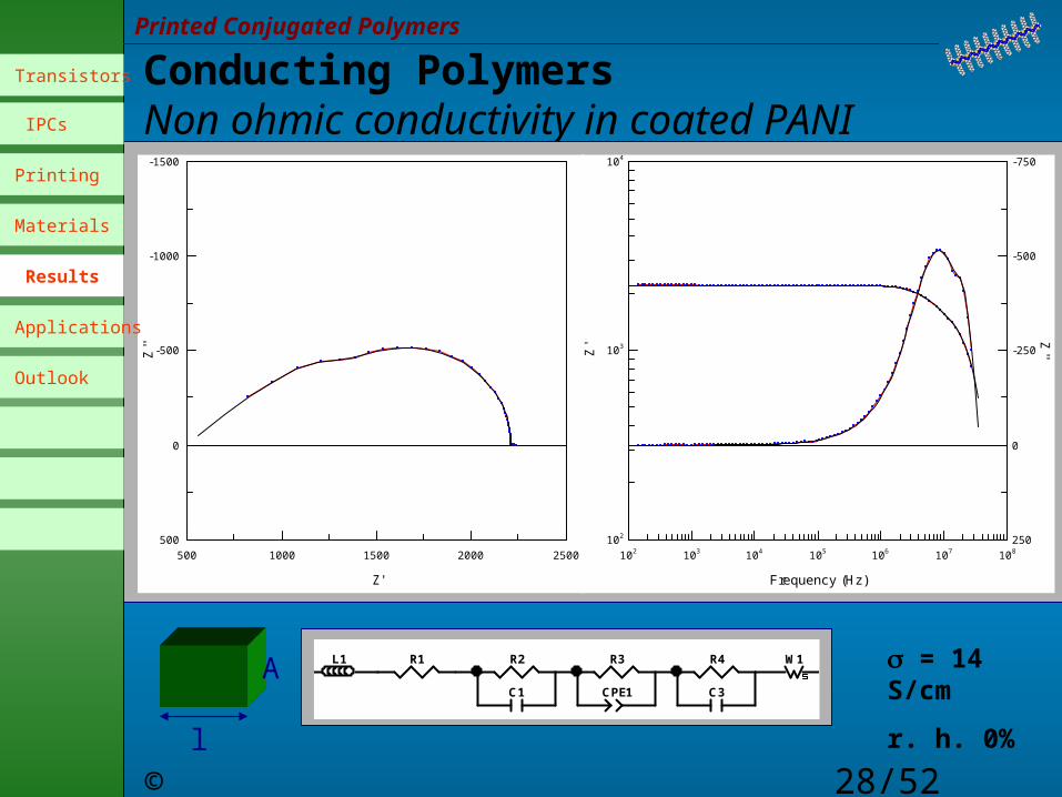
Conducting PolymersNon ohmic conductivity in coated PANI
A
l
L1 R1 R2
C1
R3
CPE1
R4
C3
W1
Element Freedom Value Error Error %L1 Free(±) 6,5029E-6 N/A N/AR1 Free(±) -1571 N/A N/AR2 Free(+) 2923 N/A N/AC1 Free(+) 9,7092E-13 N/A N/AR3 Free(+) 27,63 N/A N/ACPE1-T Free(+) 3,8108E-16 N/A N/ACPE1-P Free(+) 1,726 N/A N/AR4 Free(+) 769,2 N/A N/AC3 Free(+) 3,1075E-11 N/A N/AW1-R Free(+) 64,72 N/A N/AW1-T Free(+) 3,645E-8 N/A N/AW1-P Free(+) 0,69234 N/A N/A
Data File:Circuit Model File: C:\Documents and Settings\Sasso\Documenti\PhD\IS-data-04-07-23\Pani\Amf294\Dry\04-02-23\L-R-P1-PCPE-P2-Ws.mdlMode: Run Fitting / Selected Points (0 - 0)Maximum Iterations: 1000Optimization Iterations: 100Type of Fitting: ComplexType of Weighting: Calc-Modulus
= 14 S/cm
r. h. 0%
500 1000 1500 2000 2500
-1500
-1000
-500
0
500
Z'
Z''
102 103 104 105 106 107 108102
103
104
Frequency (Hz)Z'
-750
-500
-250
0
250
Z''
Transistors
IPCs
Printing
Materials
Results
Applications
Outlook
© Manuelli 2005
29/52
Printed Conjugated Polymers
Conducting Polymers Influence of relative humidity on conductivity
0 1000 2000 3000 4000
-4000
-3000
-2000
-1000
0
Z'
Z''
Time
= 14 S/cm at r. h. 0%
= 17.3 S/cm at r. h. 32%
Conductivity increases
Constant dedoping at r. h. 72%
Conductivity decreases
500 1000 1500 2000 2500
-1500
-1000
-500
0
500
Z'
Z'' Dry
32%
Transistors
IPCs
Printing
Materials
Results
Applications
Outlook
© Manuelli 2005
30/52
Printed Conjugated Polymers
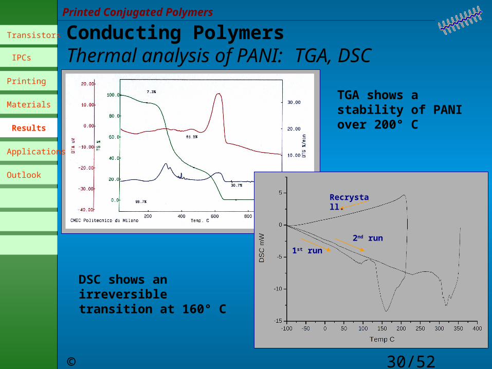
Conducting Polymers Thermal analysis of PANI: TGA, DSC
1st run
Recrystall.
2nd run
TGA shows a stability of PANI over 200° C
DSC shows an irreversible transition at 160° C
Transistors
IPCs
Printing
Materials
Results
Applications
Outlook
© Manuelli 2005
31/52
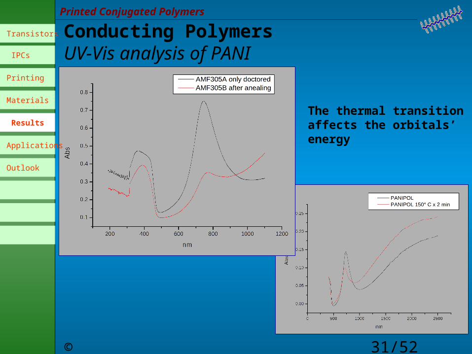
Printed Conjugated Polymers
Conducting Polymers UV-Vis analysis of PANI
The thermal transition affects the orbitals’ energy
Transistors
IPCs
Printing
Materials
Results
Applications
Outlook
© Manuelli 2005
32/52
Printed Conjugated Polymers
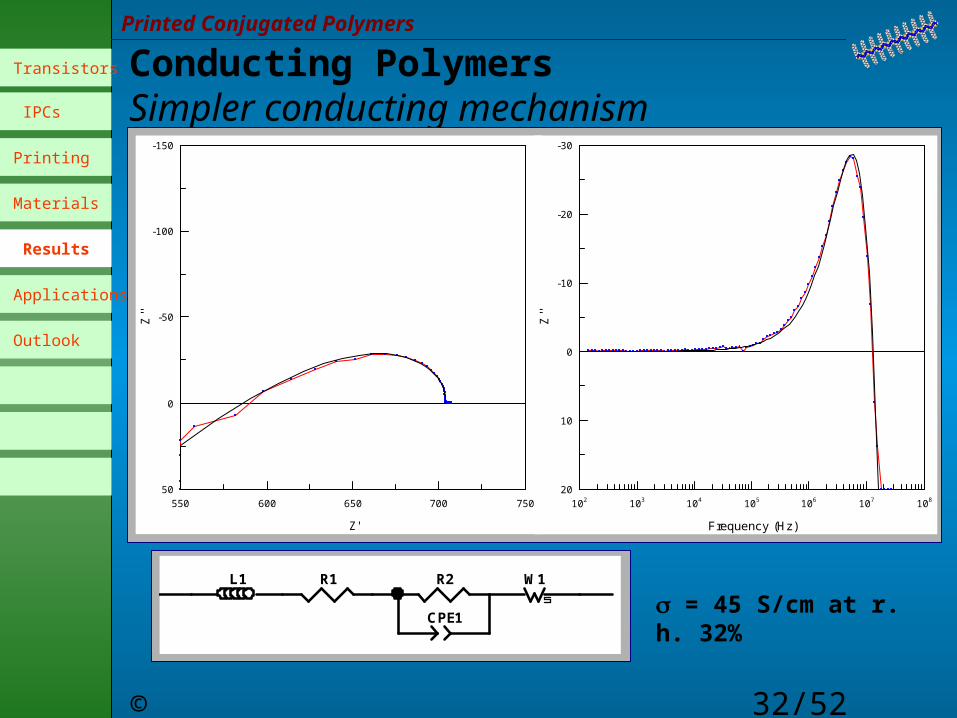
Conducting Polymers Simpler conducting mechanism
L1 R1 R2
CPE1
W1
Element Freedom Value Error Error %L1 Free(±) 2,5636E-6 N/A N/AR1 Free(±) 98,23 N/A N/AR2 Free(+) 479,3 N/A N/ACPE1-T Free(+) 3,2343E-12 N/A N/ACPE1-P Free(+) 1,058 N/A N/AW1-R Free(+) 126,6 N/A N/AW1-T Free(+) 5,0218E-8 N/A N/AW1-P Free(+) 0,48469 N/A N/A
Data File:Circuit Model File: C:\Documents and Settings\Sasso\Documenti\PhD\IS-data-04-07-23\Pani\AMF303\CaCl2\04-05-17\L-R-RCPE-Ws.mdlMode: Run Fitting / Selected Points (0 - 0)Maximum Iterations: 1000Optimization Iterations: 100Type of Fitting: ComplexType of Weighting: Calc-Modulus
550 600 650 700 750
-150
-100
-50
0
50
Z'
Z''
102 103 104 105 106 107 108
-30
-20
-10
0
10
20
Frequency (Hz)Z'
'
= 45 S/cm at r. h. 32%
Transistors
IPCs
Printing
Materials
Results
Applications
Outlook
© Manuelli 2005
33/52
Printed Conjugated Polymers
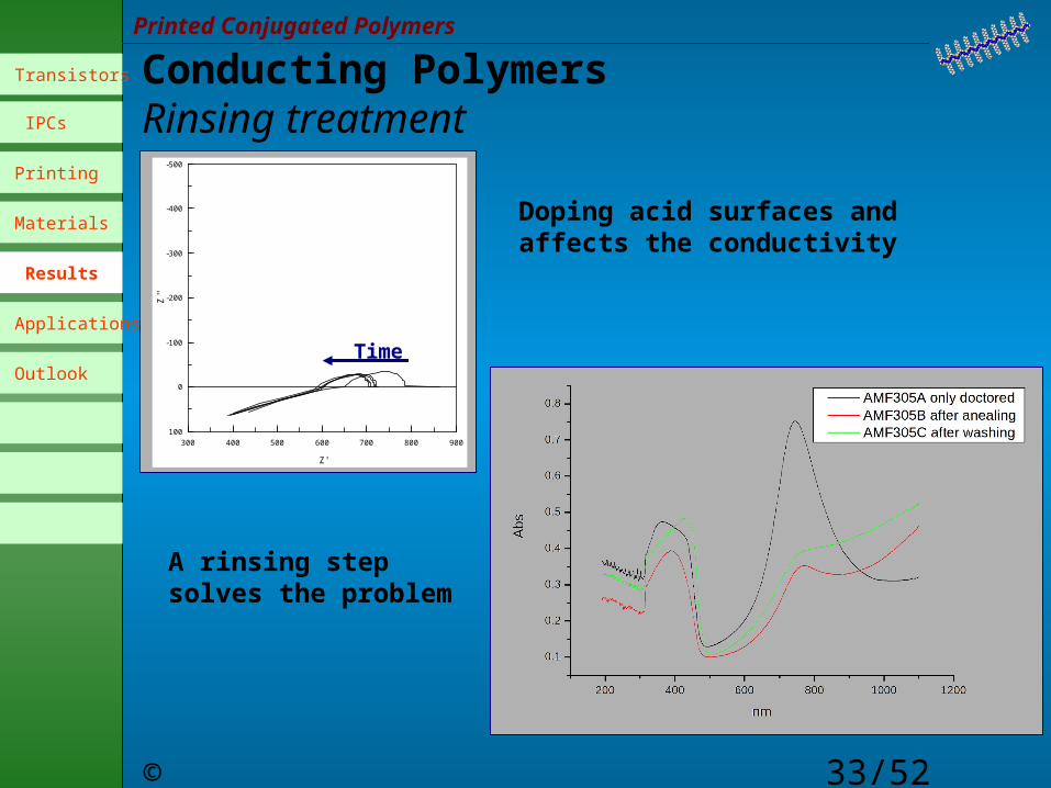
Conducting Polymers Rinsing treatment
300 400 500 600 700 800 900
-500
-400
-300
-200
-100
0
100
Z'
Z''
Time
Doping acid surfaces and affects the conductivity
A rinsing step solves the problem
Transistors
IPCs
Printing
Materials
Results
Applications
Outlook
© Manuelli 2005
34/52
Printed Conjugated Polymers
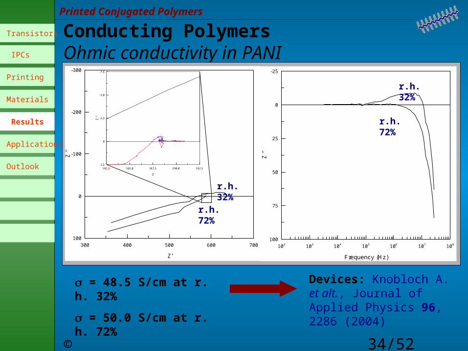
Conducting Polymers Ohmic conductivity in PANI
300 400 500 600 700
-300
-200
-100
0
100
Z'
Z''
r.h. 32%
r.h. 72%
582,5 585,0 587,5 590,0 592,5
-7,5
-5,0
-2,5
0
2,5
Z'
Z''
102 103 104 105 106 107 108
-25
0
25
50
75
100
Frequency (Hz)Z'
'
r.h. 32%
r.h. 72%
= 48.5 S/cm at r. h. 32%
= 50.0 S/cm at r. h. 72%
Devices: Knobloch A. et alt., Journal of Applied Physics 96, 2286 (2004)
Transistors
IPCs
Printing
Materials
Results
Applications
Outlook
© Manuelli 2005
35/52
Printed Conjugated Polymers
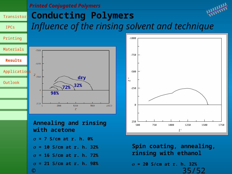
Conducting PolymersInfluence of the rinsing solvent and technique
dry32%72%
98%
500 750 1000 1250 1500 1750
-1000
-750
-500
-250
0
250
Z'Z'
'Annealing and rinsing with acetone = 7 S/cm at r. h. 0%
= 10 S/cm at r. h. 32%
= 16 S/cm at r. h. 72%
= 21 S/cm at r. h. 98%
Spin coating, annealing, rinsing with ethanol
= 20 S/cm at r. h. 32%
Transistors
IPCs
Printing
Materials
Results
Applications
Outlook
© Manuelli 2005
36/52
Printed Conjugated Polymers
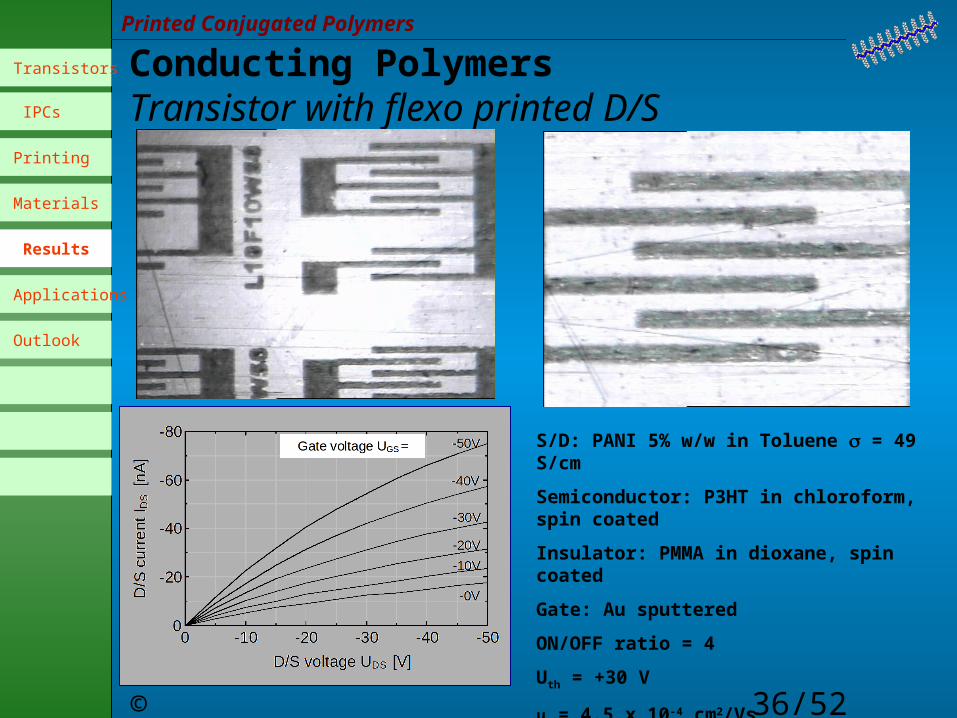
Conducting Polymers Transistor with flexo printed D/S
S/D: PANI 5% w/w in Toluene = 49 S/cm
Semiconductor: P3HT in chloroform, spin coated
Insulator: PMMA in dioxane, spin coated
Gate: Au sputtered
ON/OFF ratio = 4
Uth = +30 V
= 4.5 x 10⁻⁴ cm2/Vs
Transistors
IPCs
Printing
Materials
Results
Applications
Outlook
© Manuelli 2005
37/52
Printed Conjugated Polymers
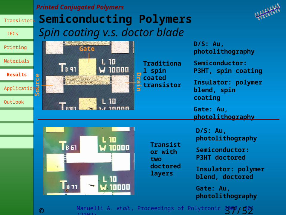
Semiconducting Polymers Spin coating v.s. doctor blade
Transistor with two doctored layers
Traditional spin coated transistor
Sour
ce
Drain
Gate
D/S: Au, photolithography
Semiconductor: P3HT doctored
Insulator: polymer blend, doctored
Gate: Au, photolithography
D/S: Au, photolithography
Semiconductor: P3HT, spin coating
Insulator: polymer blend, spin coating
Gate: Au, photolithography
Manuelli A. et alt., Proceedings of Polytronic 2002, 201 (2002)
Transistors
IPCs
Printing
Materials
Results
Applications
Outlook
© Manuelli 2005
38/52
Printed Conjugated Polymers
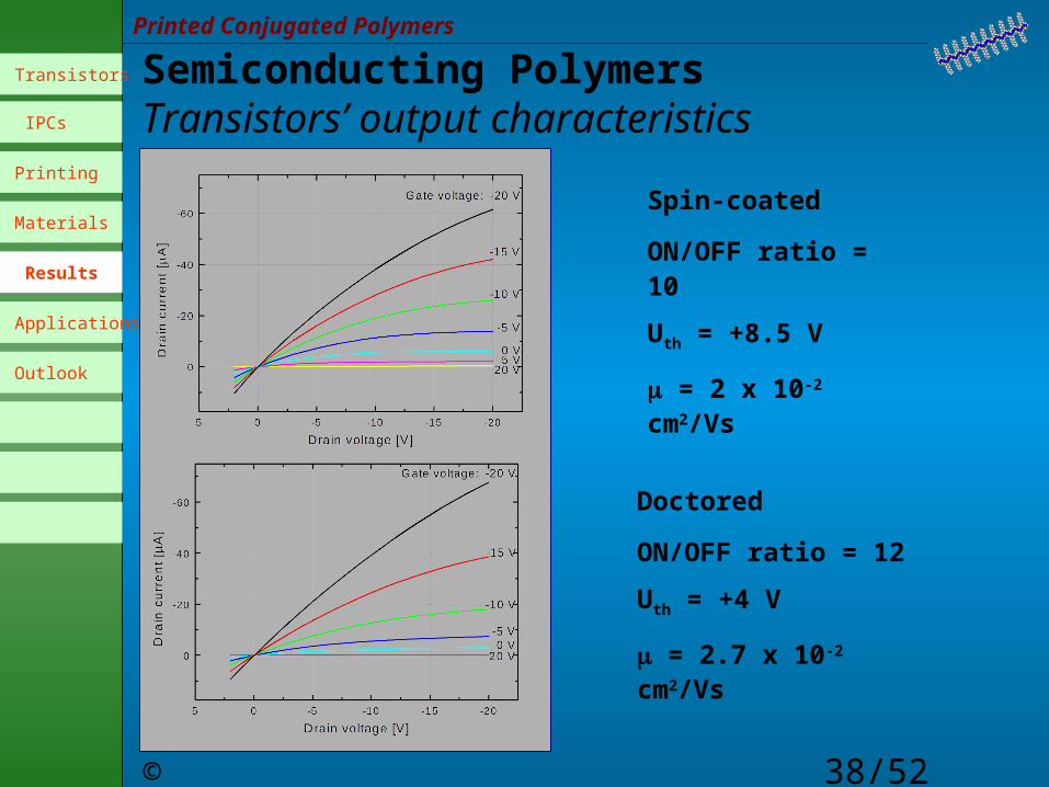
Semiconducting Polymers Transistors’ output characteristics
Doctored
ON/OFF ratio = 12
Uth = +4 V
= 2.7 x 10⁻² cm2/Vs
Spin-coated
ON/OFF ratio = 10
Uth = +8.5 V
= 2 x 10⁻² cm2/Vs
Transistors
IPCs
Printing
Materials
Results
Applications
Outlook
© Manuelli 2005
39/52
Printed Conjugated Polymers
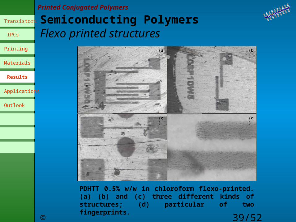
Semiconducting PolymersFlexo printed structures
PDHTT 0.5% w/w in chloroform flexo-printed. (a) (b) and (c) three different kinds of structures; (d) particular of two fingerprints.
(a) (b)
(c) (d)
Transistors
IPCs
Printing
Materials
Results
Applications
Outlook
© Manuelli 2005
40/52
Printed Conjugated Polymers
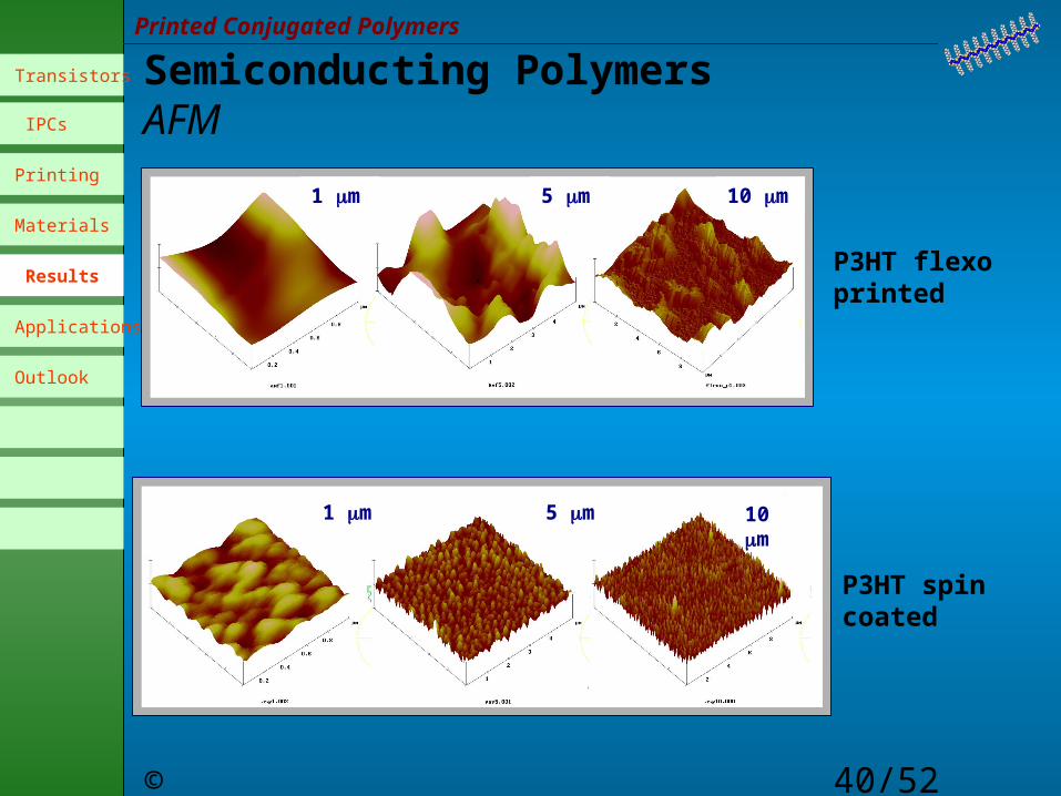
Semiconducting PolymersAFM
1 m 5 m 10 m
1 m 5 m 10 m
P3HT flexo printed
P3HT spin coated
Transistors
IPCs
Printing
Materials
Results
Applications
Outlook
© Manuelli 2005
41/52
Printed Conjugated Polymers
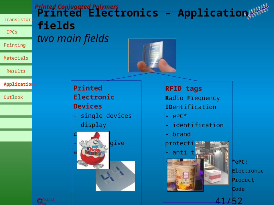
Printed Electronics – Application fieldstwo main fields
RFID tagsRadio Frequency IDentification- ePC*- identification- brand protection- anti theft- logistics
Printed ElectronicDevices- single devices- display circuits- games / give aways
*ePC:Electronic Product Code
© PolyIC 2004
Transistors
IPCs
Printing
Materials
Results
Applications
Outlook
© Manuelli 2005
42/52
Printed Conjugated Polymers
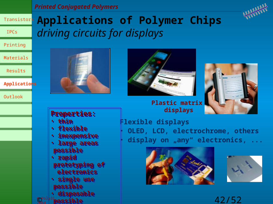
Applications of Polymer Chipsdriving circuits for displays
Plastic matrix displays
Flexible displays• OLED, LCD, electrochrome, others • display on „any“ electronics, ...
Properties:• thin• flexible • inexpensive • large areas possible• rapid prototyping of electronics
• single use possible• disposable possible
© PolyIC 2004
Transistors
IPCs
Printing
Materials
Results
Applications
Outlook
© Manuelli 2005
43/52
Printed Conjugated Polymers
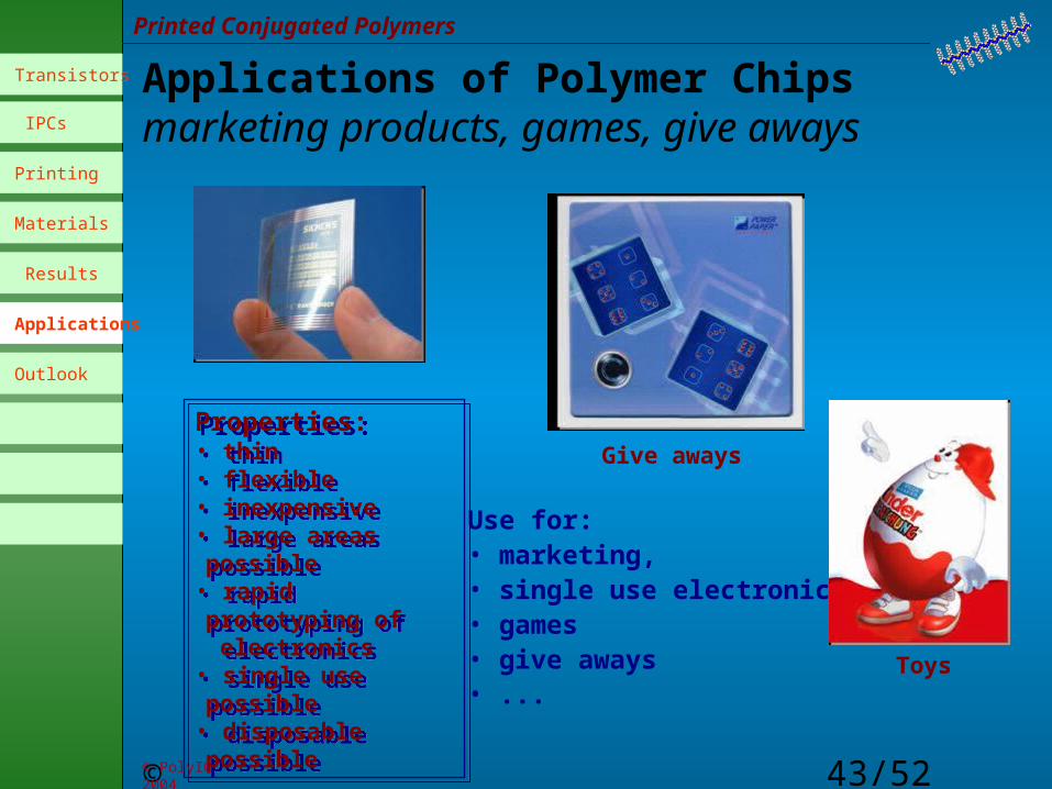
Applications of Polymer Chips marketing products, games, give aways
Toys
Give aways
Use for: • marketing, • single use electronics • games• give aways• ...
Properties:• thin• flexible • inexpensive • large areas possible• rapid prototyping of electronics
• single use possible• disposable possible
© PolyIC 2004
Transistors
IPCs
Printing
Materials
Results
Applications
Outlook
© Manuelli 2005
44/52
Printed Conjugated Polymers
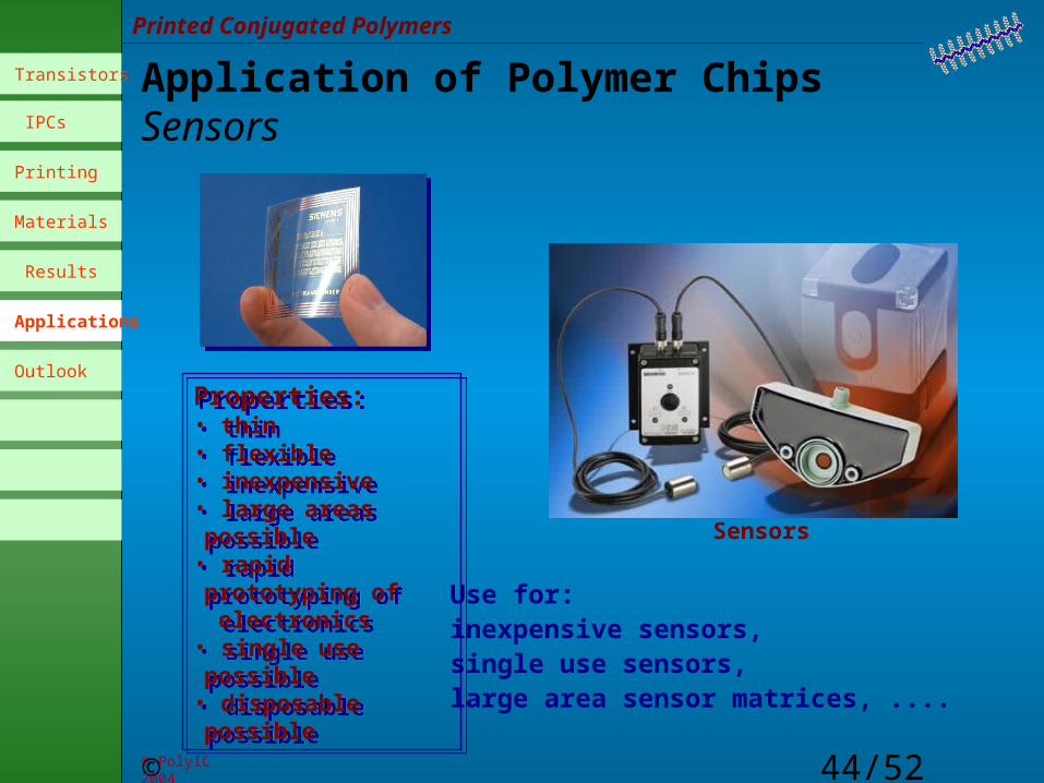
Application of Polymer ChipsSensors
Properties:• thin• flexible • inexpensive • large areas possible• rapid prototyping of electronics
• single use possible• disposable possible
Sensors
Use for: inexpensive sensors, single use sensors,large area sensor matrices, ....
© PolyIC 2004
Transistors
IPCs
Printing
Materials
Results
Applications
Outlook
© Manuelli 2005
45/52
Printed Conjugated Polymers
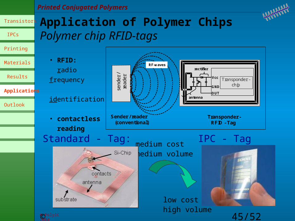
Application of Polymer ChipsPolymer chip RFID-tags
© PolyIC 2004
Sender / reader(conventional)
Transponder -RFID - Tag
send
er /
read
er Vcc
GND
OUT
rectifier
antenna
RF-waves
Transponder -chip
Standard - Tag: medium costmedium volume
IPC - Tag
low costhigh volume
• RFID: radio frequency identification
• contactless reading
Transistors
IPCs
Printing
Materials
Results
Applications
Outlook
© Manuelli 2005
46/52
Printed Conjugated Polymers
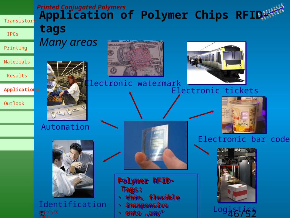
Application of Polymer Chips RFID-tagsMany areas
© PolyIC 2004
Identification
Automation
Electronic watermarkElectronic tickets
Logistics
Electronic bar code
Polymer RFID-Tags:• thin, flexible • inexpensive• onto „any“ product
Transistors
IPCs
Printing
Materials
Results
Applications
Outlook
© Manuelli 2005
47/52
Printed Conjugated Polymers
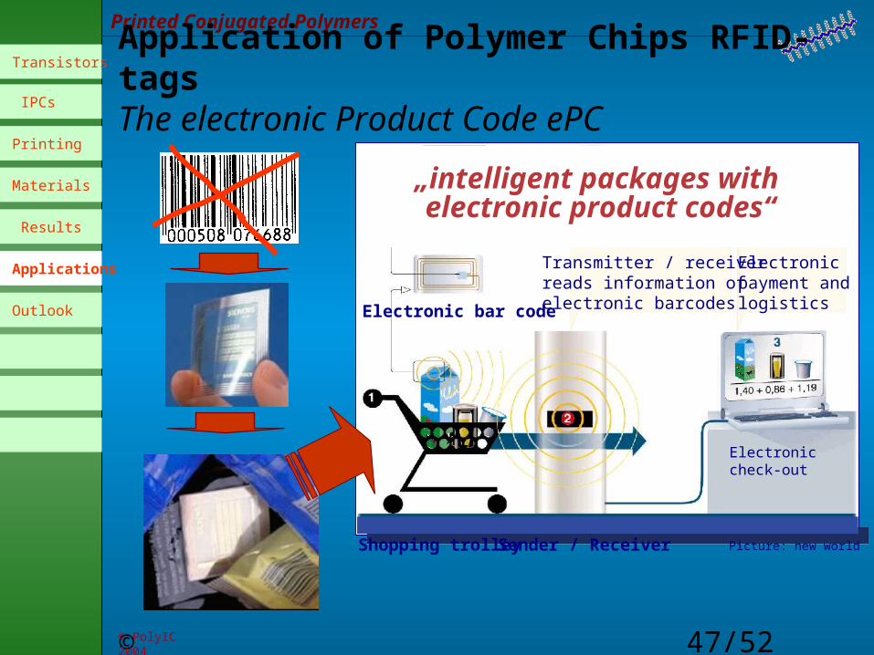
Application of Polymer Chips RFID-tagsThe electronic Product Code ePC
© PolyIC 2004
Electronic check-out
Electronic bar code
plastic transistor
Functional polymers
Transmitter / receiverreads information of electronic barcodes
Electronic payment andlogistics
Shopping trolley Sender / Receiver
„intelligent packages with electronic product codes“
Picture: new world
Transistors
IPCs
Printing
Materials
Results
Applications
Outlook
© Manuelli 2005
48/52
Printed Conjugated Polymers
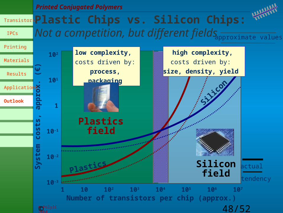
Plastic Chips vs. Silicon Chips: Not a competition, but different fields
Number of transistors per chip (approx.)
Syst
em c
osts
, app
rox.
(€)
Plasticsfield
Siliconfield
1 10 103
10-1
10-2
10-3
102
1
101
102 104 105 106 107
Plastics
Silicon
low complexity, costs driven by:
process, packaging
actual
tendency
high complexity,costs driven by:
size, density, yield
approximate values
© PolyIC 2004
Transistors
IPCs
Printing
Materials
Results
Applications
Outlook
© Manuelli 2005
49/52
Printed Conjugated Polymers
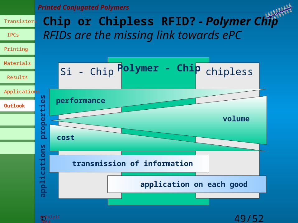
Chip or Chipless RFID? - Polymer ChipRFIDs are the missing link towards ePC
performance
volume
cost
transmission of information
application on each good
Si - Chip Polymer - Chip chipless
prop
ertie
sap
plic
atio
ns
© PolyIC 2004
Transistors
IPCs
Printing
Materials
Results
Applications
Outlook
© Manuelli 2005
50/52
Printed Conjugated Polymers
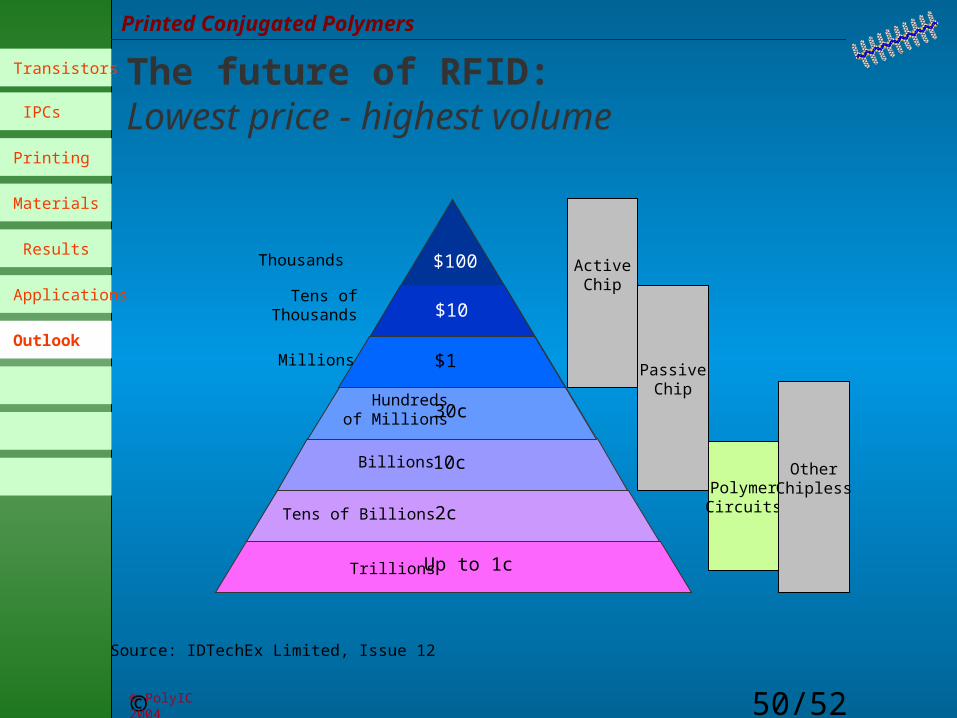
The future of RFID:Lowest price - highest volume
Trillions
Tens of Billions
Billions
Hundredsof Millions
Millions
Tens ofThousands
Thousands
2c
10c
30c
$1
$10
$100
Up to 1c
ActiveChip
PassiveChip
PolymerCircuits
OtherChipless
Source: IDTechEx Limited, Issue 12
© PolyIC 2004
Transistors
IPCs
Printing
Materials
Results
Applications
Outlook
© Manuelli 2005
51/52
Printed Conjugated Polymers
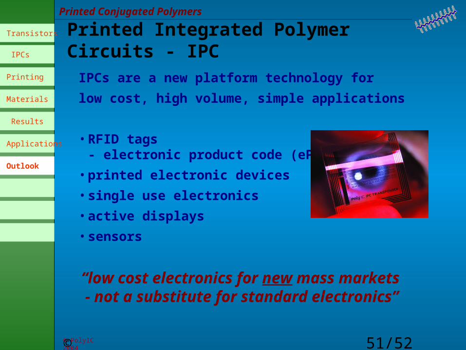
IPCs are a new platform technology forlow cost, high volume, simple applications
• RFID tags- electronic product code (ePC)
• printed electronic devices• single use electronics• active displays • sensors
“low cost electronics for new mass markets - not a substitute for standard electronics”
Printed Integrated Polymer Circuits - IPC
© PolyIC 2004
Transistors
IPCs
Printing
Materials
Results
Applications
Outlook
© Manuelli 2005
52/52
Printed Conjugated Polymers
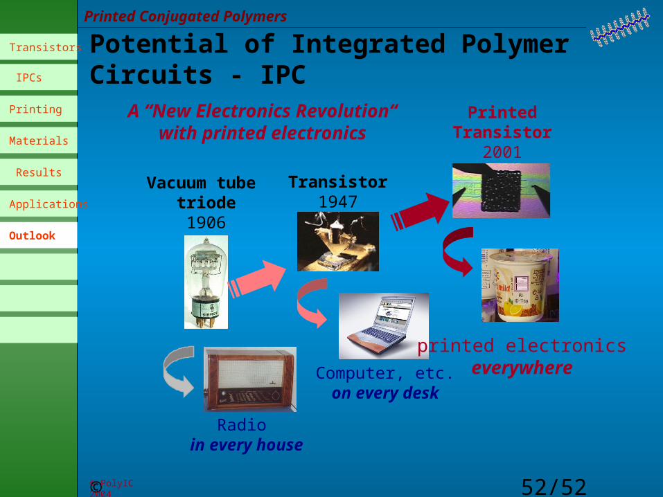
A “New Electronics Revolution“ with printed electronics
Vacuum tube triode1906
Transistor1947
Radio in every house
Computer, etc.on every desk
printed electronicseverywhere
PrintedTransistor
2001
© PolyIC 2004
Transistors
IPCs
Printing
Materials
Results
Applications
Outlook
Potential of Integrated Polymer Circuits - IPC


![Poe 2004 Phylogeny of Anoles[1]](https://img.pdfslide.net/doc/110x75/577cdaad1a28ab9e78a63b09/poe-2004-phylogeny-of-anoles1.jpg)