Embed Size (px)
DESCRIPTION
Solution manual for modern processor design by john paul shen and mikko h. lipasti
Citation preview
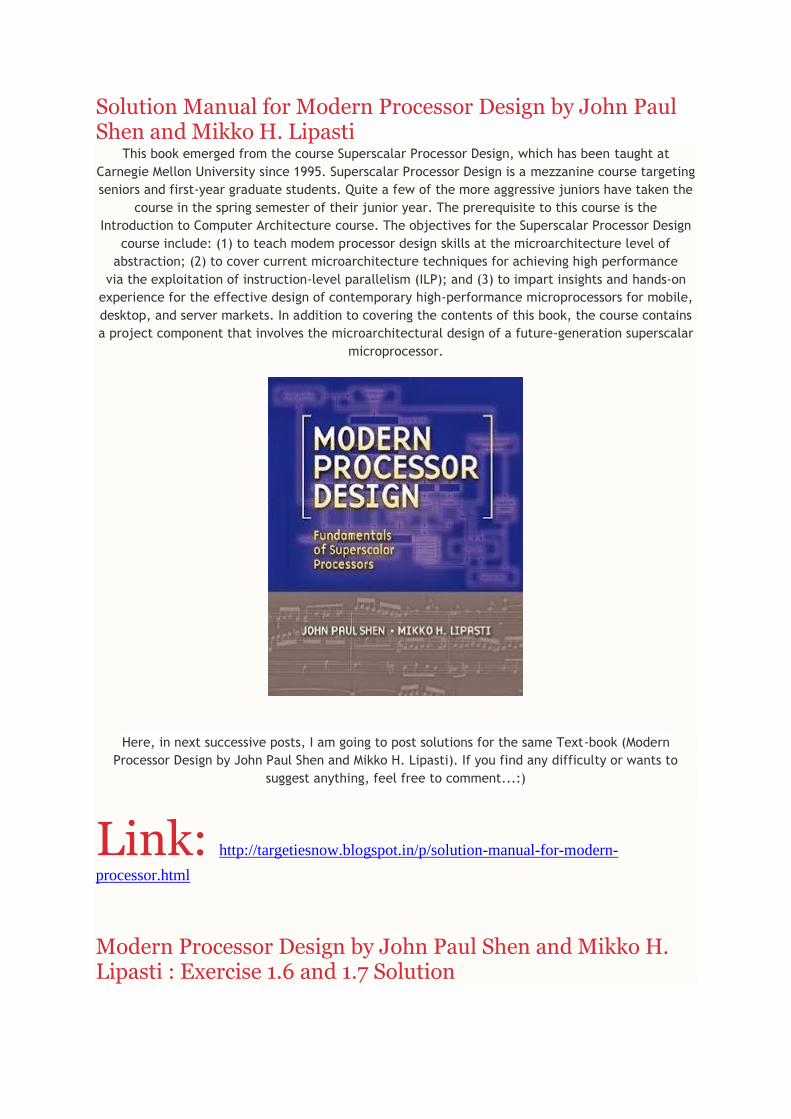
Solution Manual for Modern Processor Design by John Paul Shen and Mikko H. Lipasti
This book emerged from the course Superscalar Processor Design, which has been taught at
Carnegie Mellon University since 1995. Superscalar Processor Design is a mezzanine course targeting
seniors and first-year graduate students. Quite a few of the more aggressive juniors have taken the
course in the spring semester of their junior year. The prerequisite to this course is the
Introduction to Computer Architecture course. The objectives for the Superscalar Processor Design
course include: (1) to teach modem processor design skills at the microarchitecture level of
abstraction; (2) to cover current microarchitecture techniques for achieving high performance
via the exploitation of instruction-level parallelism (ILP); and (3) to impart insights and hands-on
experience for the effective design of contemporary high-performance microprocessors for mobile,
desktop, and server markets. In addition to covering the contents of this book, the course contains
a project component that involves the microarchitectural design of a future-generation superscalar
microprocessor.
Here, in next successive posts, I am going to post solutions for the same Text-book (Modern
Processor Design by John Paul Shen and Mikko H. Lipasti). If you find any difficulty or wants to
suggest anything, feel free to comment...:)
Link: http://targetiesnow.blogspot.in/p/solution-manual-for-modern-
processor.html Modern Processor Design by John Paul Shen and Mikko H. Lipasti : Exercise 1.6 and 1.7 Solution
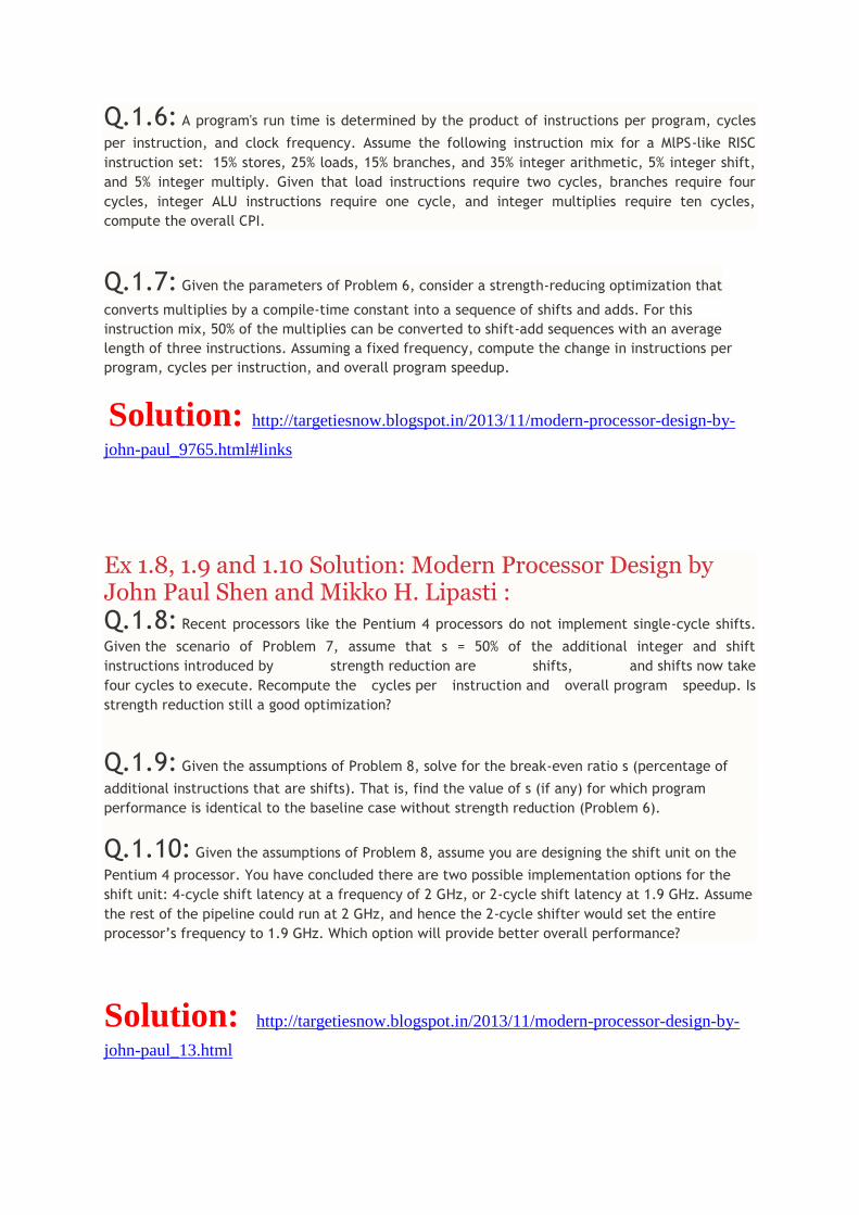
Q.1.6: A program's run time is determined by the product of instructions per program, cycles
per instruction, and clock frequency. Assume the following instruction mix for a MlPS-like RISC
instruction set: 15% stores, 25% loads, 15% branches, and 35% integer arithmetic, 5% integer shift,
and 5% integer multiply. Given that load instructions require two cycles, branches require four
cycles, integer ALU instructions require one cycle, and integer multiplies require ten cycles,
compute the overall CPI.
Q.1.7: Given the parameters of Problem 6, consider a strength-reducing optimization that
converts multiplies by a compile-time constant into a sequence of shifts and adds. For this
instruction mix, 50% of the multiplies can be converted to shift-add sequences with an average
length of three instructions. Assuming a fixed frequency, compute the change in instructions per
program, cycles per instruction, and overall program speedup.
Solution: http://targetiesnow.blogspot.in/2013/11/modern-processor-design-by-
john-paul_9765.html#links
Ex 1.8, 1.9 and 1.10 Solution: Modern Processor Design by John Paul Shen and Mikko H. Lipasti : Q.1.8: Recent processors like the Pentium 4 processors do not implement single-cycle shifts.
Given the scenario of Problem 7, assume that s = 50% of the additional integer and shift
instructions introduced by strength reduction are shifts, and shifts now take
four cycles to execute. Recompute the cycles per instruction and overall program speedup. Is
strength reduction still a good optimization?
Q.1.9: Given the assumptions of Problem 8, solve for the break-even ratio s (percentage of
additional instructions that are shifts). That is, find the value of s (if any) for which program
performance is identical to the baseline case without strength reduction (Problem 6).
Q.1.10: Given the assumptions of Problem 8, assume you are designing the shift unit on the
Pentium 4 processor. You have concluded there are two possible implementation options for the
shift unit: 4-cycle shift latency at a frequency of 2 GHz, or 2-cycle shift latency at 1.9 GHz. Assume
the rest of the pipeline could run at 2 GHz, and hence the 2-cycle shifter would set the entire
processor’s frequency to 1.9 GHz. Which option will provide better overall performance?
Solution: http://targetiesnow.blogspot.in/2013/11/modern-processor-design-by-
john-paul_13.html
Q.2.4: Consider that you would like to add a load-immediate instruction to the TYP instruction
set and pipeline. This instruction extracts a 16-bit immediate value from the instruction word, sign-
extends the immediate value to 32 bits, and stores the result in the destination register specified in
the instruction word. Since the extraction and sign-extension can be
accomplished without the ALU, your colleague suggests that such instructions be able to
write their results into the register in the decode (ID) stage. Using the hazard
detection algorithm described in Figure 2-15, identify what additional hazards such a change might
introduce.
Q.2.5: Ignoring pipeline interlock hardware (discussed in Problem 6), what additional
pipeline resources does the change outline in Problem 4 require? Discuss these resources and
their cost.
Q.2.6: Considering the change outlined in Problem 4, redraw the pipeline interlock
hardware shown in Figure 2-18 to correctly handle the load-immediate instructions.
Solution: http://targetiesnow.blogspot.in/2013/11/ex-24-25-26-solution-modern-
processor.html
Ex 2.8, 2.9 & 2.15 Solution : Modern Processor Design by John Paul Shen and Mikko H. Lipasti :
Q.2.8: Consider adding a store instruction with indexed addressing mode to
the TYP pipeline. This store differs from the existing store with
register+immediate addressing mode by computing its effective address as the sum
of two source registers, that is, stx r3, r4, r5 performs r3<-MEM[r4+r5]. Describe
the additional pipeline resources needed to support such an instruction in the TYP
pipeline. Discuss the advantages and disadvantages of such an instruction.
Q.2.9: Consider adding a load-update instruction with register+immediate and postupdate
addressing mode. In this addressing mode, the effective address for the load is computed as
register+immediate, and the resulting address is written back into the base register. That is, lwu
r3,8(r4) performs r3<-MEM[r4+8]; r4<r4+8. Describe the additional pipeline resources needed to
support such an instruction in the TYP pipeline.
Q.2.15: The IBM study of pipelined processor performance assumed an instruction mix based
on popular C programs in use in the 1980s. Since then, object oriented languages like C++ and Java
have become much more common. One of the effects of these languages is that object inheritance
and polymorphism can be used to replace conditional branches with virtual function calls. Given
the IBM instruction mix and CPI shown in the following table, perform the following transformations
to reflect the use of C++/Java, and recompute the overall CPI and speedup or slowdown due to this
change:
• Replace 50% of taken conditional branches with a load instruction followed by a jump register
instruction
(the load and jump register implement a virtual function call).
• Replace 25% of not-taken branches with a load instruction followed by a jump register
instruction.
Solution: http://targetiesnow.blogspot.in/2013/11/ex-28-29-215-solution-modern-
processor.html
Q.2.16: In a TYP-based pipeline design with a data cache, load
instructions check the tag array for a cache hit in parallel with accessing
the data array to read the corresponding memory location. Pipelining stores
to such a cache is more difficult, since the processor must check the tag
first, before it overwrites the data array. Otherwise, in the case of a cache
miss, the wrong memory location may be overwritten by the store. Design a
solution to this problem that does not require sending the store down the
pipe twice, or stalling the pipe for every store instruction. Referring to
Figure 2-15, are there any new RAW, WAR, and/or WAW memory
hazards?
Q.2.17: The MIPS pipeline shown in Table 2-7 employs a two-phase
clocking scheme that makes efficient use of a shared TLB, since instruction
fetch accesses the TLB in phase one and data fetch accesses in phase
two. However, when resolving a conditional branch, both the branch target
address and the branch fall-through address need to be translated during
phase one in parallel with the branch condition check in phase one of the
ALU stage to enable instruction fetch from either the target or the fall-
through during phase two. This seems to imply a dual-ported TLB. Suggest
an architected solution to this problem that avoids dual-porting the TLB.
Solution: http://targetiesnow.blogspot.in/2013/11/ex-216-217-solution-modern-
processor.html
Q.3.1: Given the following benchmark code, and
assuming a virtually-addressed fully-associative cache
with infinite capacity and 64 byte blocks, compute the
overall miss rate (number of misses divided by number
of references). Assume that all variables except array
locations reside in registers, and that arrays A, B,
and C are placed consecutively in memory. double A[1024], B[1024], C[1024]; for(int i=0;i<1000;i += 2) { A[i] = 35.0 * B[i] + C[i+1]; }
Q.3.3: Given the example code in Problem 1, and
assuming a virtually-addressed two-way set
associative cache of capacity 8KB and 64 byte blocks,
compute the overall miss rate (number of misses divided
by number of references). Assume that all variables
except array locations reside in registers, and that
arrays A, B, and C are placed consecutively in memory.
Solution: http://targetiesnow.blogspot.in/2013/11/ex-31-33-solution-modern-
processor.html
Q.3.4: Consider a cache with 256 bytes. Word size is 4 bytes and block size is 16 bytes. Show
the values in the cache and tag bits after each of the following memory access operations for the
two cache organizations direct mapped and 2-way associative. Also indicate whether the access
was a hit or a miss. Justify. The addresses are in hexadecimal representation. Use LRU (least
recently used) replacement algorithm wherever needed.
1.Read 0010
2.Read 001C
3.Read 0018
4.Write 0010
5.Read 0484
6.Read 051C
7.Read 001C
8.Read 0210
9.Read 051C
Solution: http://targetiesnow.blogspot.in/2013/11/modern-processor-design-by-
john-paul_1.html
Ex. 3.13 Solution : Modern Processor Design by John Paul Shen and Mikko H. Lipasti : Solution Manual Q.3.13: Consider a processor with 32-bit virtual addresses, 4KB pages and 36-bit physical
addresses. Assume memory is byte-addressable (i.e. the 32-bit VA specifies a byte in memory).
L1 instruction cache: 64 Kbytes, 128 byte blocks, 4-way set associative, indexed and tagged with
virtual address.
L1 data cache: 32 Kbytes, 64 byte blocks, 2-way set associative, indexed and tagged with physical
address, write-back.
4-way set associative TLB with 128 entries in all. Assume the TLB keeps a dirty bit, a reference bit,
and 3 permission bits (read, write, execute) for each entry.
Specify the number of offset, index, and tag bits for each of these structures in the table below.
Also, compute the total size in number of bit cells for each of the tag and data arrays.
Solution: http://targetiesnow.blogspot.in/2013/11/ex-313-solution-modern-
processor-design.html
Q.3.16: Assume a two-level cache hierarchy with a private level one
instruction cache (L1I), a private level one data cache (L1D), and a shared
level two data cache (L2). Given local miss rates for the 4% for L1I, 7.5%
for L1D, and 35% for L2, compute the global miss rate for the L2 cache.
Q.3.17: Assuming 1 L1I access per instruction and 0.4 data accesses
per instruction, compute the misses per instruction for the L1I, L1D, and L2 caches of Problem 16.
Q.3.18: Given the miss rates of Problem 16, and assuming that
accesses to the L1I and L1 D caches take one cycle, accesses to the L2 take 12 cycles, accesses to main memory take 75 cycles, and a clock rate of 1GHz, compute the average memory reference latency for this cache
hierarchy.
Q.3.19: Assuming a perfect cache CPI (cycles per instruction) for a
pipelined processor equal to 1.15 CPI, compute the MCPI and overall CPI
for a pipelined processor with the memory hierarchy described in Problem 18 and the miss rates and access rates specified in Problem 16 and Problem 17.
Solution: http://targetiesnow.blogspot.in/2013/11/ex-316-317-318-and-319-
solution-modern.html
Q.3.28: Assume a synchronous front-side processor-
memory bus that operates at 100 Hz and has an 8-byte
data bus. Arbitration for the bus takes one bus cycle
(10 ns), issuing a cache line read command for 64
bytes of data takes one cycle, memory controller
latency (including DRAM access) is 60 ns, after which
data double words are returned in back-to back cycles.
Further assume the bus is blocking or circuit-

switched. Compute the latency to fill a single 64-byte
cache line. Then compute the peak read bandwidth for
this processor-memory bus, assuming the processor
arbitrates for the bus for a new read in the bus cycle
following completion of the last read.
Q.3.31: Consider finite DRAM bandwidth at a memory
controller, as follows. Assume double-data-rate DRAM
operating at 100 MHz in a parallel non-interleaved
organization, with an 8 byte interface to the DRAM
chips. Further assume that each cache line read results
in a DRAM row miss, requiring a precharge and RAS
cycle, followed by row-hit CAS cycles for each of the
double words in the cache line. Assuming memory
controller overhead of one cycle (10 ns) to initiate a
read operation, and one cycle latency to transfer data
from the DRAM data bus to the processor-memory bus,
compute the latency for reading one 64 byte cache
block. Now compute the peak data bandwidth for the
memory interface, ignoring DRAM refresh cycles.
Solution: http://targetiesnow.blogspot.in/2013/11/ex-328-and-331-modern-
processor-design.html
Q.3.28: Assume a synchronous front-side processor-memory bus that
operates at 100 Hz and has an 8-byte data bus. Arbitration for the bus
takes one bus cycle (10 ns), issuing a cache line read command for 64
bytes of data takes one cycle, memory controller latency (including
DRAM access) is 60 ns, after which data double words are returned in back-
to back cycles. Further assume the bus is blocking or circuit-
switched. Compute the latency to fill a single 64-byte cache line. Then
compute the peak read bandwidth for this processor-memory bus, assuming
the processor arbitrates for the bus for a new read in the bus cycle
following completion of the last read.
Q.3.34: Assume a single-platter disk drive with an average seek time
of 4.5 ms, rotation speed of 7200 rpm, data transfer rate of 10 Mbytes/s
per head, and controller overhead and queueing of 1 ms. What is the
average access latency for a 4096-byte read?
Q.3.35: Recompute the average access latency for Problem 34 assuming

a rotation speed of 15 K rpm, two platters, and an average seek time of 4.0
ms.
Solution: http://targetiesnow.blogspot.in/2013/11/ex-328-334-and-335-solution-
modern.html
Ex 4.8 Solution : Modern Processor Design by John Paul Shen and Mikko H. Lipasti : Solution manual Q.4.8: In an in-order pipelined processor, pipeline latches are used to hold result operands
from the time an execution unit computes them until they are written back to the register file
during the writeback stage. In an out-of-order processor, rename registers are used for the same
purpose. Given a four-wide out-of-order processor TYP
pipeline, compute the minimum number of rename registers needed
to prevent rename register starvation from limiting concurrency. What happens to this number if
frequency demands force a designer to add five extra pipeline stages between
dispatch and execute, and five more stages between execute and retire/writeback?
Solution: http://targetiesnow.blogspot.in/2013/11/modern-processor-design-by-
john-paul.html
Ex 5.1 and 5.2 Solution : Modern Processor Design by John Paul Shen and Mikko H. Lipasti : Solution manual Q.5.1: The displayed code that follows steps through the elements of two arrays (A[] and B[])
concurrently, and for each element, it puts the larger of the two values into the corresponding
element of a third array (C[]). The three arrays are of length N.
The instruction set used for Problems 5.1 through 5.6 is as follows:
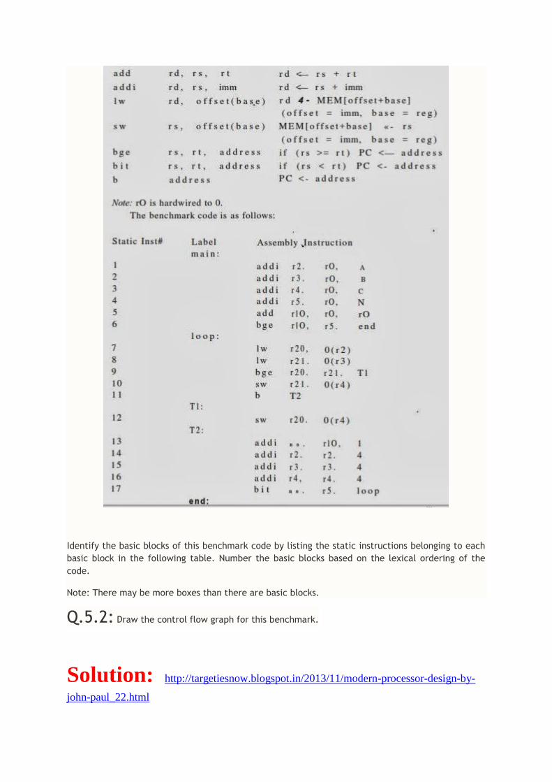
Identify the basic blocks of this benchmark code by listing the static instructions belonging to each
basic block in the following table. Number the basic blocks based on the lexical ordering of the
code.
Note: There may be more boxes than there are basic blocks.
Q.5.2: Draw the control flow graph for this benchmark.
Solution: http://targetiesnow.blogspot.in/2013/11/modern-processor-design-by-
john-paul_22.html

Ex 5.7 through 5.13 Solution : Modern Processor Design by John Paul Shen and Mikko H. Lipasti : Solution manual
Q.5.7 through Problem 5.13: Consider the following code segment within a
loop body for problems 5: if (x is even) then (branch b1) increment a (b1 taken) if (x is a multiple of 10) then (branch b2) increment b (b2 taken)
Assume that the following list of 9 values of x is to be processed by 9 iterations of this loop.
8, 9, 10, 11, 12, 20, 29, 30, 31
Note: assume that predictor entries are updated by each dynamic branch before the next dynamic branch accesses the predictor (i.e., there is no update delay).
Q.5.7: Assume that an one-bit (history bit) state machine (see above) is used as the
prediction algorithm for predicting the execution of the two branches in this loop. Indicate the predicted and actual branch directions of the b1 and b2 branch instructions for each iteration of this loop. Assume initial state of 0, i.e., NT, for the predictor.
Q.5.8: What are the prediction accuracies for b1 and b2?
Q.5.9: What is the overall prediction accuracy?
Q.5.10: Assume a two-level branch prediction scheme is used. In addition to the one-
bit predictor, a one bit global register (g) is used. Register g stores the direction of the last branch
executed (which may not be the same branch as the branch currently being
predicted) and is used to index into two separate one-bit branch history tables (BHTs) as
shown below. Depending on the value of g, one of the two BHTs is selected and used to
do the normal one-bit prediction. Again, fill in the predicted and actual branch directions
of b1 and b2 for nine iterations of the loop. Assume the initial value of g = 0, i.e., NT.
For each prediction, depending on the current value of g, only one of the two BHTs is
accessed and updated. Hence, some of the entries below should be empty.
Note: assume that predictor entries are updated by each dynamic branch before the next
dynamic branch accesses the predictor (i.e. there is no update delay).
Q.5.11: What are the prediction accuracies for b1 and b2?
Q.5.12: What is the overall prediction accuracy?
Q.5.13: What is the prediction accuracy of b2 when g = 0? Explain why.
Solution: http://targetiesnow.blogspot.in/2013/11/ex-57-through-513-solution-
modern.html
Exercise 5.14 Solution : Modern Processor Design by John Paul Shen and Mikko H. Lipasti : Solution manual
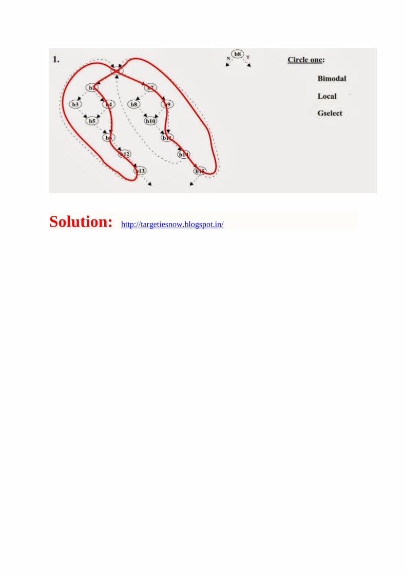
Q.5.14: Below is the control flow graph of a simple program. The CFG is annotated with three
different execution trace paths. For each execution trace circle which branch predictor (bimodal, local, or Gselect) will best predict the branching behavior of the given trace. More than one predictor may perform equally well on a particular trace. However, you are to use each of the three predictors exactly once in choosing the best predictors for the three traces. Circle your choice for each of the three traces and add. (Assume each trace is executed many times and every node in the CFG is a conditional branch. The branch history register for the local, global, and Gselect predictors is limited to 4 bits.)
Solution: http://targetiesnow.blogspot.in/