Embed Size (px)
Citation preview
Diode equivalent circuit load line analysis diode as a switch
Basic electronics engineering
By Tanya makkar Btech cse 1(3 semester)A12405215003
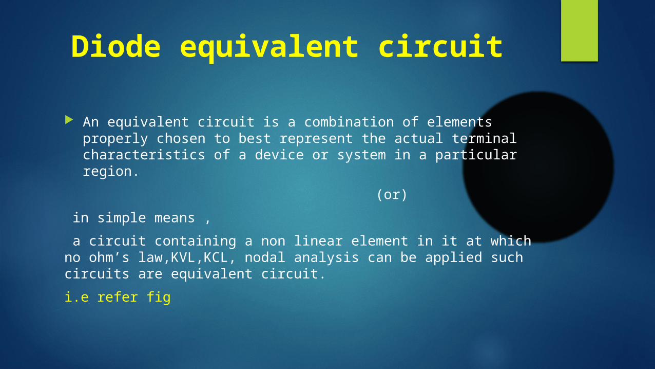
Diode equivalent circuit
An equivalent circuit is a combination of elements properly chosen to best represent the actual terminal characteristics of a device or system in a particular region.
(or) in simple means , a circuit containing a non linear element in it at which no ohm’s law,KVL,KCL, nodal analysis can be applied such circuits are equivalent circuit. i.e refer fig
Diode equivalent circuit
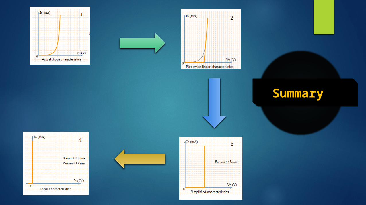
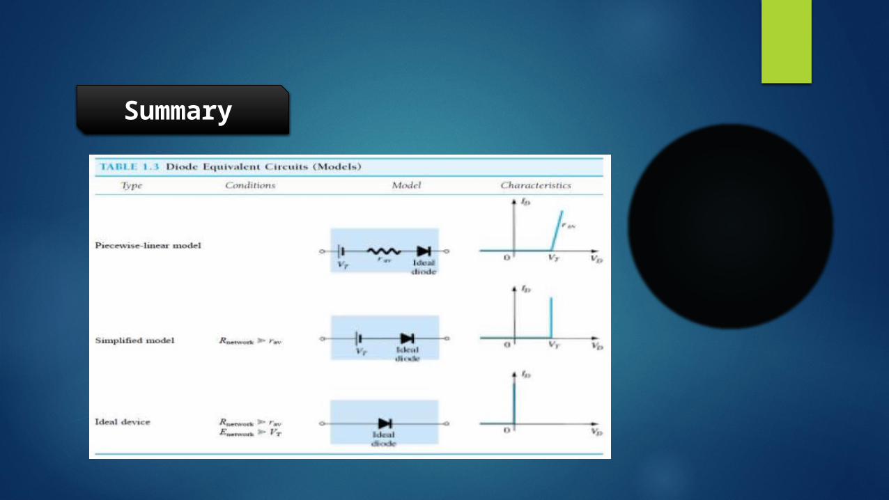
Piecewise linear
equivalent circuitSimplified equivalent circuits
Ideal equivalent circuits
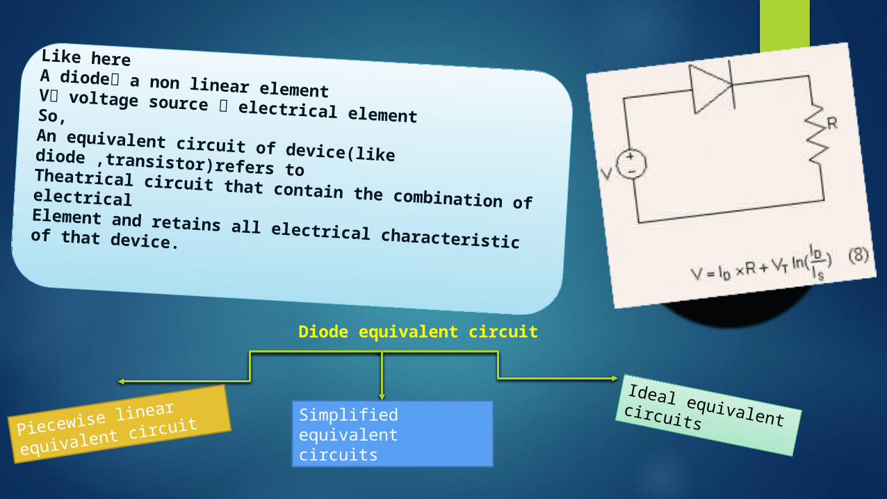
Like hereA diode a non linear element V voltage source electrical elementSo,An equivalent circuit of device(like diode ,transistor)refers toTheatrical circuit that contain the combination of electrical Element and retains all electrical characteristic of that device.
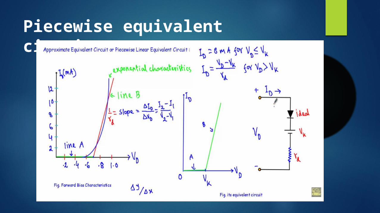
Piecewise equivalent circuits
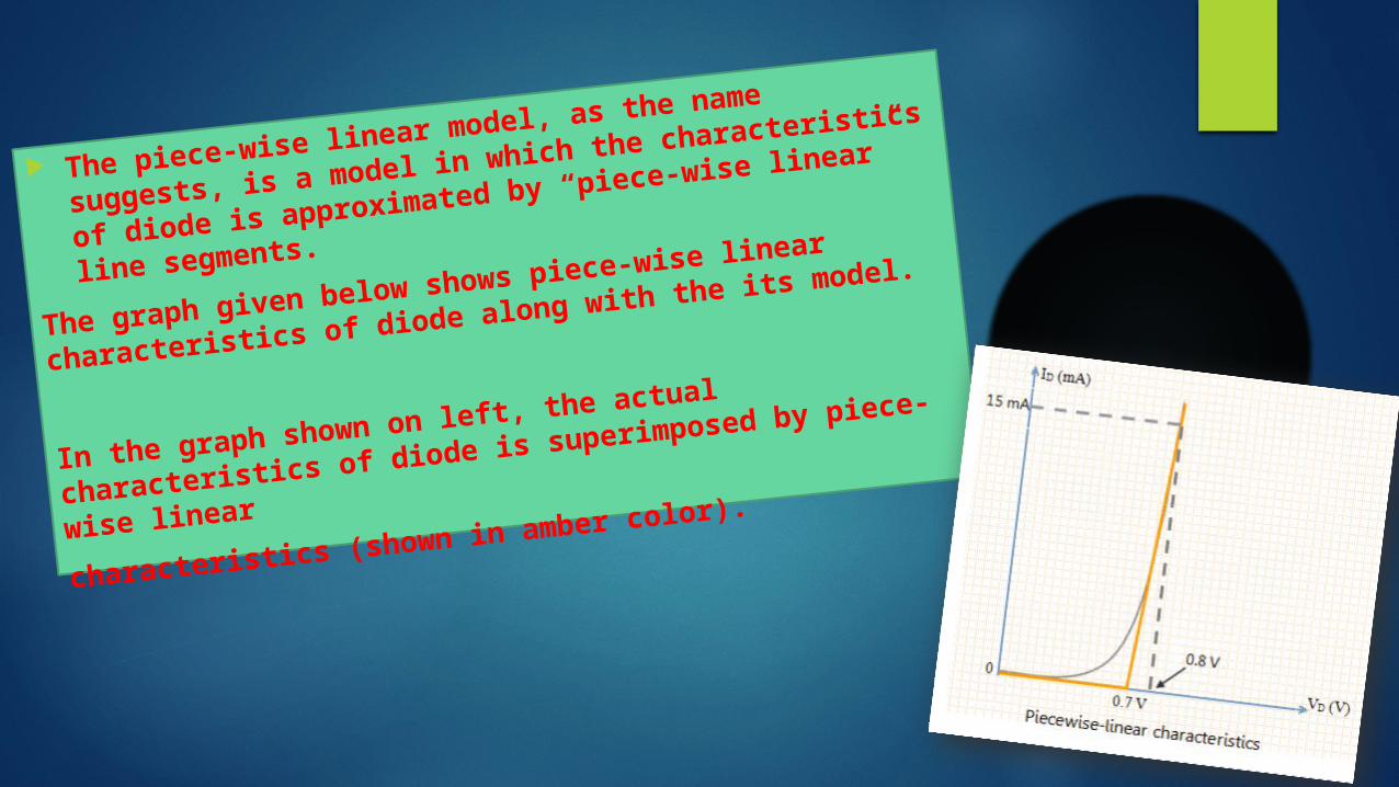
The piece-wise linear model, as the name suggests,
is a model in which the characteristics of diode is
approximated by “piece-wise linear” line segments.
The graph given below shows piece-wise linear
characteristics of diode along with the its model.
In the graph shown on left, the actual characteristics
of diode is superimposed by piece-wise linear
characteristics (shown in amber color).
Piecewise equivalent circuits
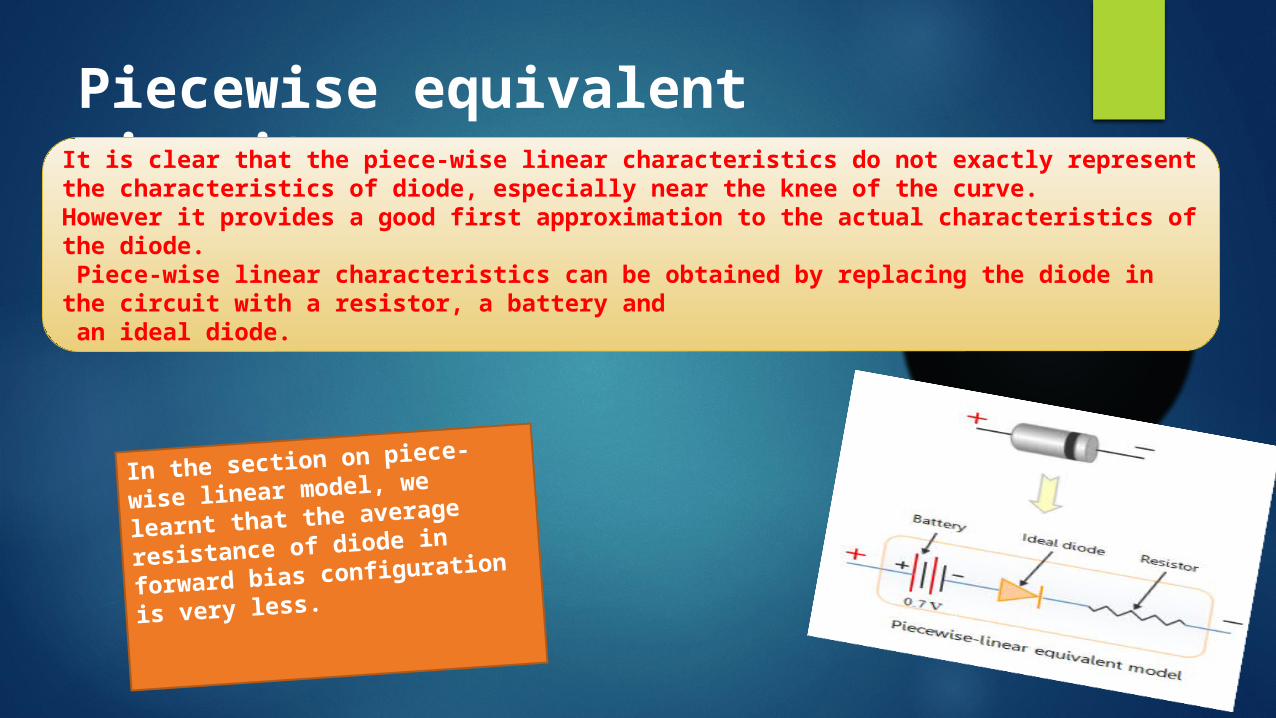
In the section on piece-wise
linear model, we learnt that
the average resistance of
diode in forward bias
configuration is very less.
It is clear that the piece-wise linear characteristics do not exactly represent the characteristics of diode, especially near the knee of the curve. However it provides a good first approximation to the actual characteristics of the diode. Piece-wise linear characteristics can be obtained by replacing the diode in the circuit with a resistor, a battery and an ideal diode.
Simplified equivalent circuit
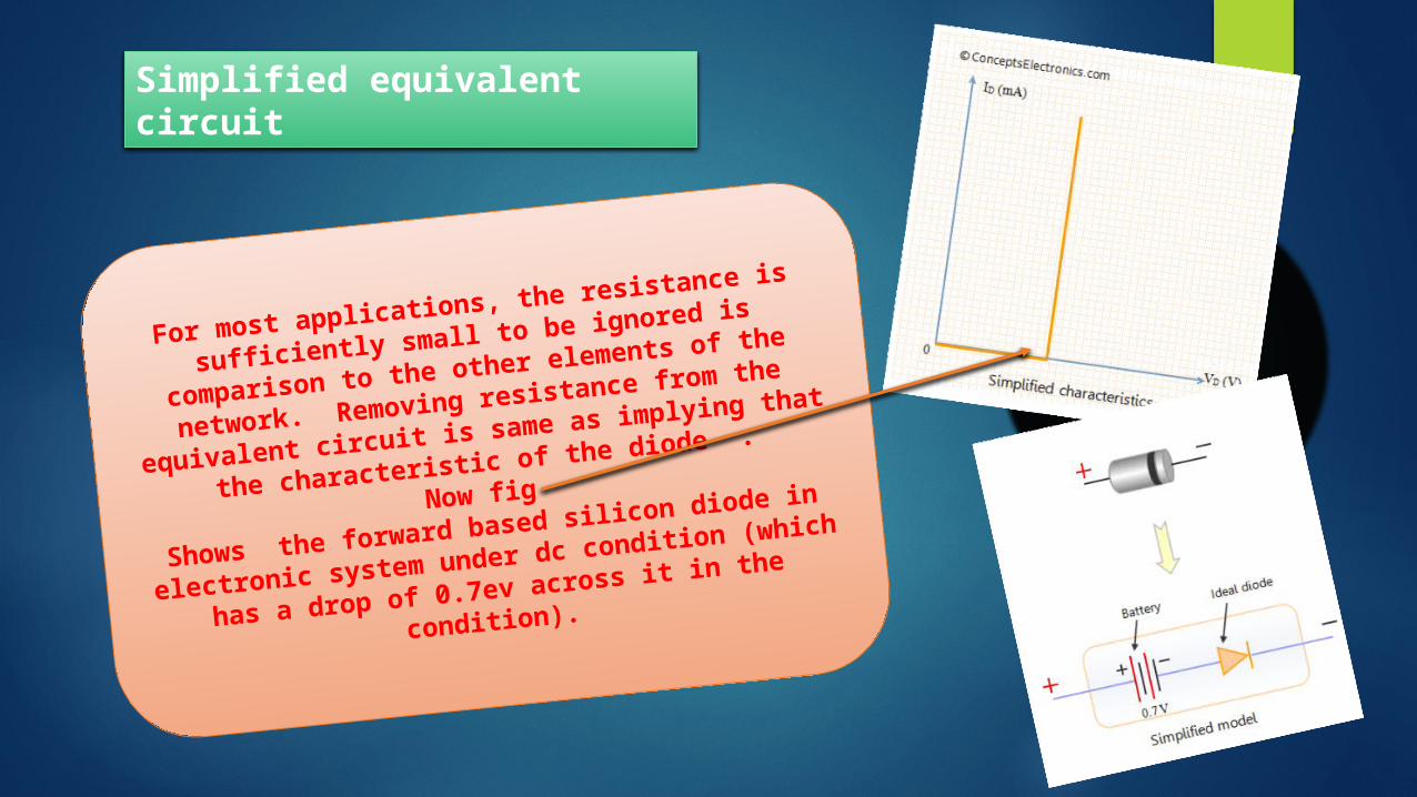
For most applications, the resistance is
sufficiently small to be ignored is comparison
to the other elements of the network.
Removing resistance from the equivalent
circuit is same as implying that the
characteristic of the diode .
Now fig
Shows the forward based silicon diode in
electronic system under dc condition (which
has a drop of 0.7ev across it in the condition).
Ideal equivalent diode
The piece-wise linear model represents the diode model in piece-wise linear manner. The simplified diode model ignores the effect of
diode resistance in comparison with values of other elements of the circuit.
Lets take the process of simplification one step further and establish that the voltage drop across the diode (0.7 V for Si) is negligible as compared to other voltage drops in the
circuit. Hence the diode voltage drop can be ignored for
simplification purpose. The resultant model is an ideal diode model.
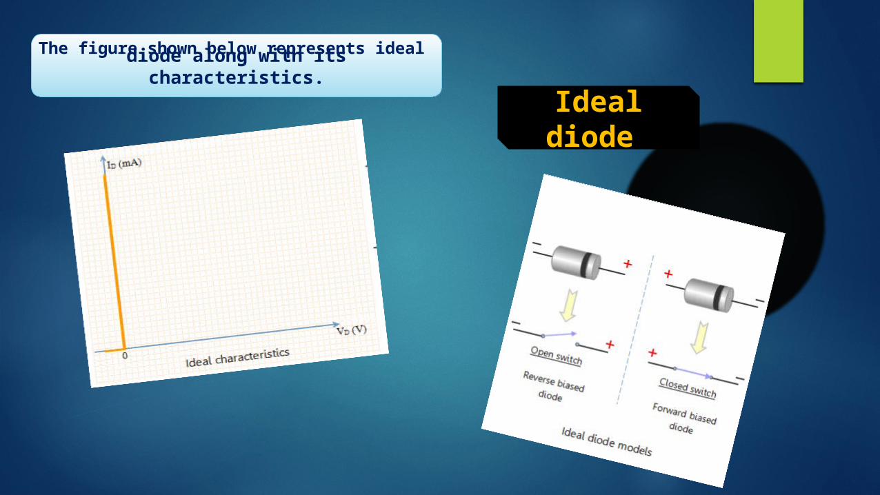
diode along with its characteristics.The figure shown below represents ideal
Ideal diode
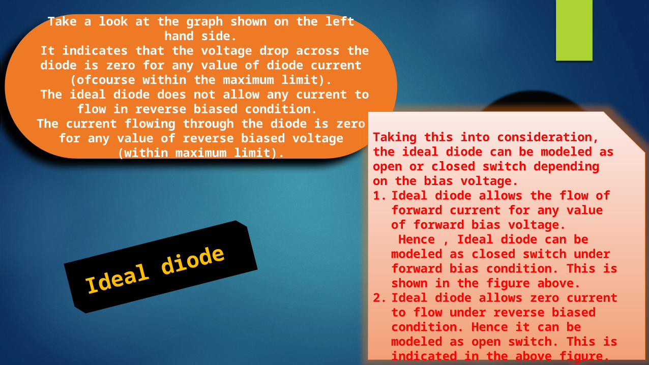
Take a look at the graph shown on the left hand side.
It indicates that the voltage drop across the diode is zero for any value of diode current
(ofcourse within the maximum limit). The ideal diode does not allow any current to
flow in reverse biased condition. The current flowing through the diode is zero for
any value of reverse biased voltage (within maximum limit).
Taking this into consideration, the ideal diode can be modeled as open or closed switch depending on the bias voltage.1. Ideal diode allows the flow of forward
current for any value of forward bias voltage. Hence , Ideal diode can be modeled as closed switch under forward bias condition. This is shown in the figure above.
2. Ideal diode allows zero current to flow under reverse biased condition. Hence it can be modeled as open switch. This is indicated in the above figure.
Ideal diode
Summary
Load line
analysis
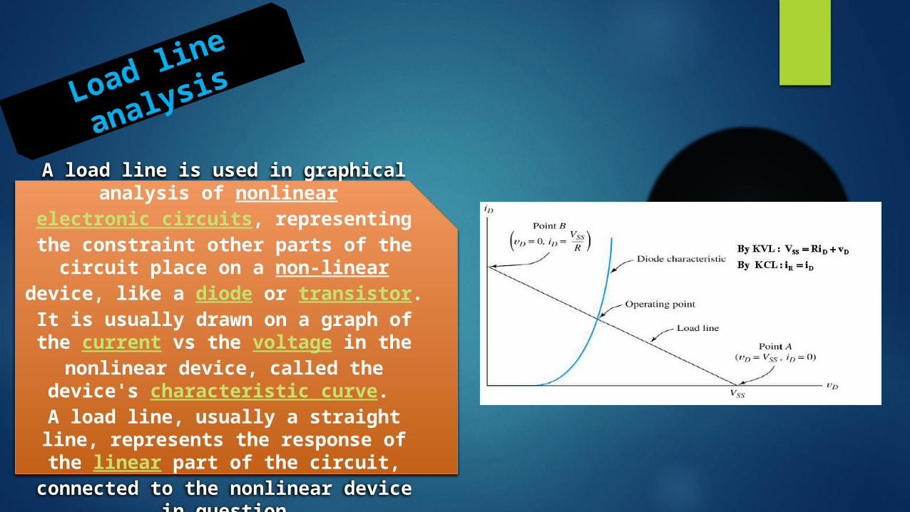
A load line is used in graphical analysis of nonlinear
electronic circuits, representing the constraint other parts of the circuit place on a non-linear device, like a
diode or transistor. It is usually drawn on a graph of the
current vs the voltage in the nonlinear device, called the device's
characteristic curve. A load line, usually a straight line,
represents the response of the linear part of the circuit, connected to the
nonlinear device in question
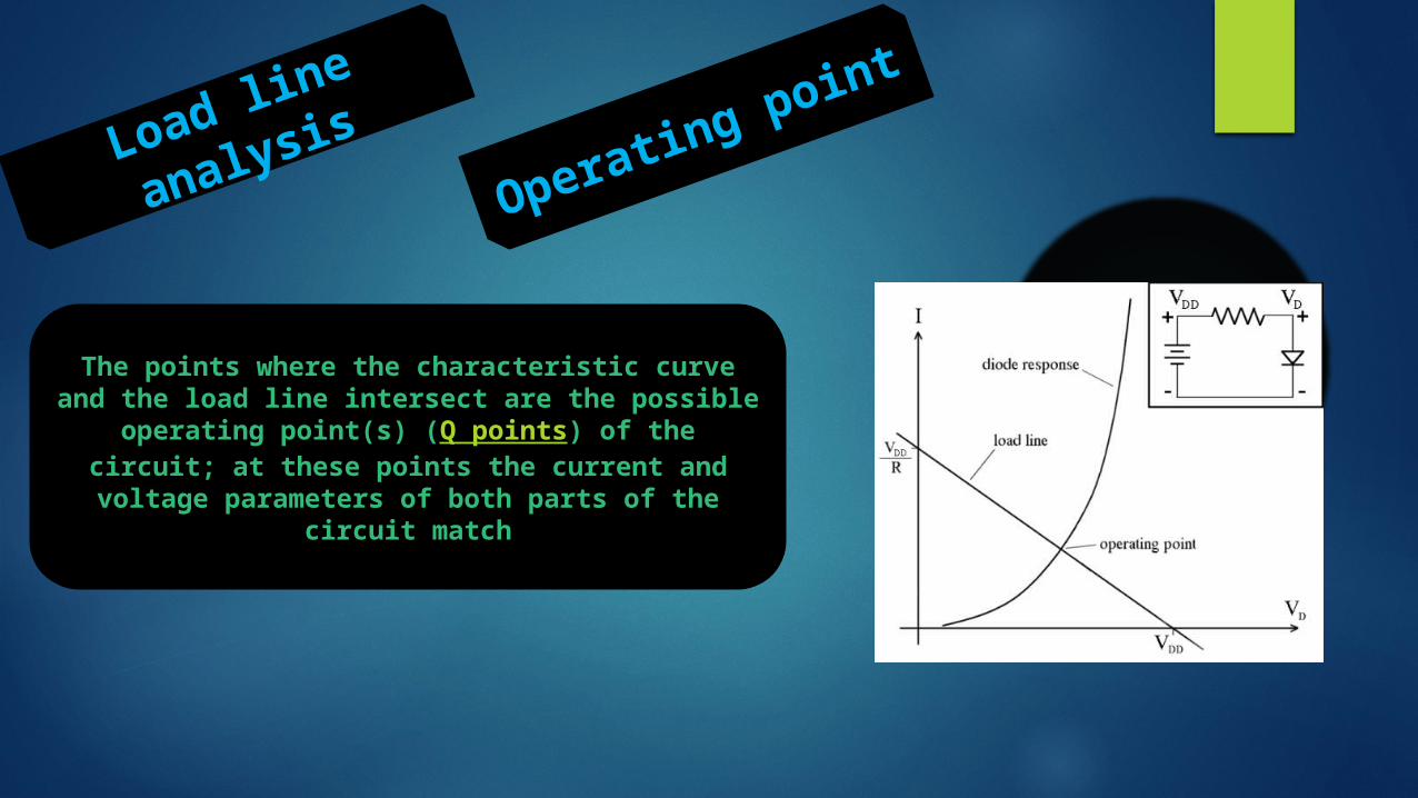
Load line
analysisOperating point
The points where the characteristic curve and the load line intersect are the possible
operating point(s) (Q points) of the circuit; at these points the current and voltage
parameters of both parts of the circuit match
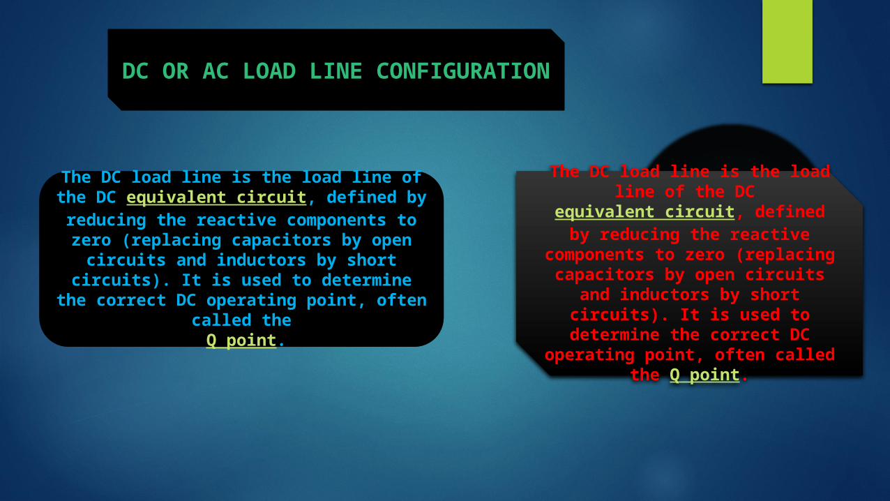
DC OR AC LOAD LINE CONFIGURATION
The DC load line is the load line of the DC equivalent circuit, defined by
reducing the reactive components to zero (replacing capacitors by open
circuits and inductors by short circuits). It is used to determine the
correct DC operating point, often called the Q point.
The DC load line is the load line of the DC equivalent circuit,
defined by reducing the reactive components to zero (replacing capacitors by open circuits and inductors by short
circuits). It is used to determine the correct DC
operating point, often called the Q point.
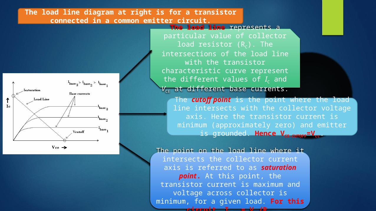
The load line diagram at right is for a transistor connected in a common emitter circuit.
The load line represents a particular value of collector load resistor (RC).
The intersections of the load line with the transistor characteristic curve represent the different values of IC and VCE at different base currents.
The point on the load line where it intersects the collector current axis is
referred to as saturation point. At this point, the transistor current is maximum and voltage across collector is minimum, for a given load. For this circuit, IC-SAT=
VCC/RC.
The cutoff point is the point where the load line intersects with the collector voltage axis. Here the transistor current is minimum (approximately zero)
and emitter is grounded. Hence VCE-CUTOFF=Vcc.
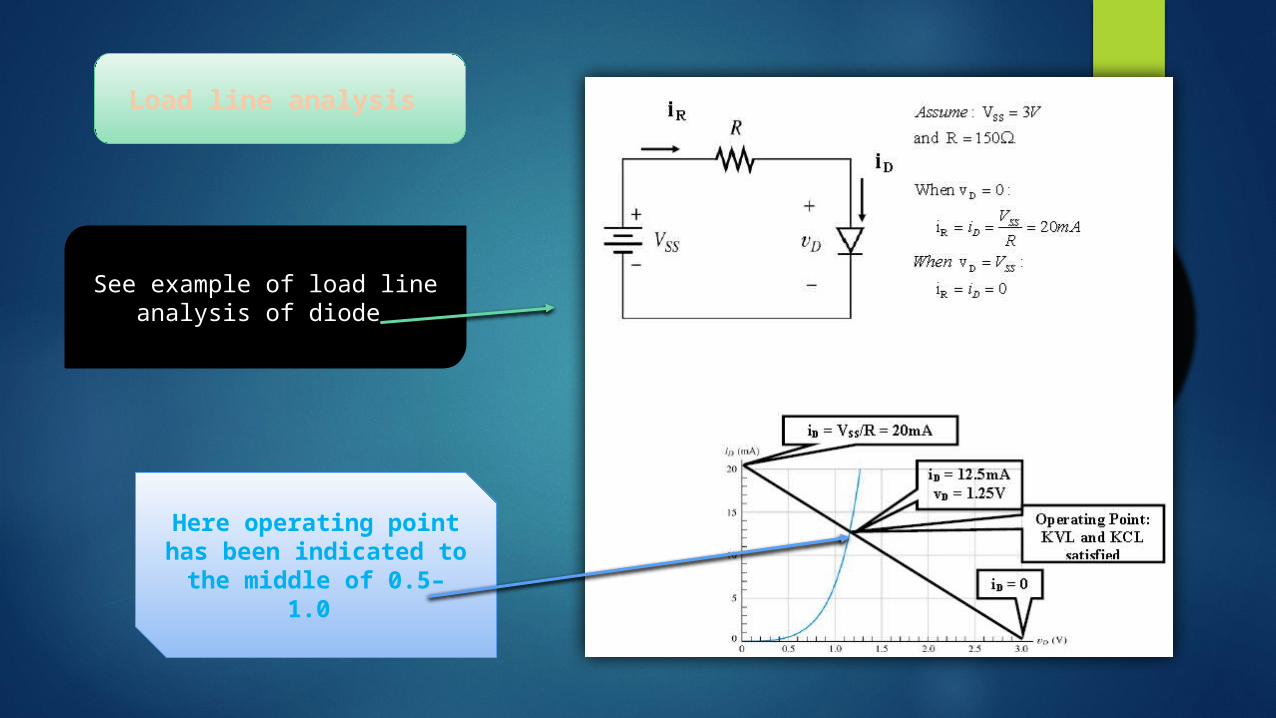
See example of load line analysis of diode
Here operating point has been indicated to the middle of 0.5– 1.0
Load line analysis
Diode as a switch
What is a Switching Diode?Switching diodes are a single p-n diode in a discrete package. A switching diode provides the same functionality as a switch. It has high resistance below the specified applied voltage similar to an open switch, whereas above that voltage it changes in a sudden way to the low resistance of a closed switch. Switching diodes are used in devices such as ring modulation

Applications for Switching Diodes:The switching diode is the most basic function of almost every electronic application. Switching diodes are also used in high-speed rectifying applications, such as in radiofrequency receivers. Applications also include high-speed switching, general-purpose switching and reverse polarity protection in the consumer, automotive, and telecommunication industry.
Types of Switching Diodes There are many different kinds of switching diodes. At Future Electronics we stock many of the most common types categorized by power dissipation, maximum reverse recovery time, maximum reverse voltage, maximum average forward current, packaging type and maximum peak current. The parametric filters on our website can help refine your search results depending on the required specifications. The most common values for power dissipation are 200 mW, 250 mW, 350 mW and 500 mW. We also carry switching diodes with power dissipation as high as 1 kW. Maximum reverse recovery time can have a range from 1 ns to 50 us, with the most common maximum reverse recovery time being 4 ns.
Summary