Embed Size (px)
Citation preview
IOSR Journal of Mechanical and Civil Engineering (IOSR-JMCE)
e-ISSN: 2278-1684,p-ISSN: 2320-334X, Volume 9, Issue 3 (Sep. - Oct. 2013), PP 49-57 www.iosrjournals.org
www.iosrjournals.org 49 | Page
Design & Simulation of RISC Processor using Hyper
Pipelining Technique
SimranRana, Rajesh Mehra Assistant Professor in HIET (ECE) Shahpur, Distt.-Kangra H.P, INDIA
Associate Professor in NITTTR Chd. (ECE) Sec.-26, INDIA
Abstract: This Hyper pipelining technique is different to the pipelining of instruction decoding known from
RISC processors. The point is that we can use hyper pipelining on top of any sequential logic, for example a
RISC processor, independent of its underlying functionality. The RISC processor with pipelined instruction set
decoding can automatically be hyper pipelined to generate CMF individual RISC processors. Hyper pipelining implements additional register and can use register balancing for fine grain timing optimizations. The method
hyper pipelining is also called “C-slow Retiming”. The main benefit is the multiplication of the core's
functionality by only implementing registers. This is a great advantage for ASICs but obviously very attractive
for FPGAs with their already existing registers.
Keywords: RISC Processor, Decomposition of Sequential Circuits, Hyper Pipelining, Retiming, C-Slow
Retiming.
I. Introduction [1]
Now a day’s developments are taking place at a very rapid rate. Market is becoming more and more
customer driven. Customer wants system designed tailor made to suit his needs. This is putting great pressure on
the embedded system designer. After finding appropriate processor its development and debugging tools and the
associated learning curve becomes time consuming. Looking into this factor and looking at the advancements in the field Of VLSI design, the days are no longer that people will start implementing their own processor
supporting desired instructions only along with associated peripherals. Due to the need to meet increasingly
challenging objectives of increasing performance, reducing power consumption and reducing size, synchronous
processor core designs have been increasing significantly in complexity for some time now. This applies to even
those designs originally based on the RISC principle of reducing complexity in order to improve instruction
throughput and the performance of the design. Not only does the methodology of this paper provide a
standardized approach for describing that it generates can be used as a basis for the formal verification of the
design; and thus facilitate solutions to the problems that increasing complexity poses for traditional validation.
II. Role Of VVLSI In Designing The Processor For designing the system various methods are available like traditional method of designing,
microprocessor and
Microcontroller based design etc and now a day’s VLSI design method is mostly preferred because of
its no. of advantages, such as Small size, Low power dissipation,
Operate at high speed, Security up to 20 years, Reprogramming is possible for more than 20,000 times,
Fast concurrent programming, It is having internet reconfigurable logic, Remote load programming is possible,
Time to market is small, Cost to performance ratio is high, Easy up gradations to new specifications. The main
factor for preferring VLSI design is a single chip solution, which is supporting to create our own processor.
VLSI has made possible to have digital hardware implementation, which can be changed as per customer
requirement. Different descriptive languages are available with different types of design entry such as VHDL
[Very high speed integrated circuit Hardware Description Language], Verilog and ABEL
Design & Simulation of RISC Processor using Hyper Pipelining Technique
www.iosrjournals.org 50 | Page
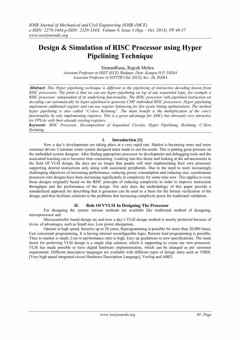
III. System Architecture With Pipeline [2]
Fig 1: Five-Stage pipelined structure of RISC (super pipelining)
The instruction fetch stage is also responsible for reading the instruction memory and sending the current
instruction to the next stage in the pipeline, or a stall if a branch has been detected in order to avoid incorrect
execution. The instruction fetch unit contains the following logic elements that are implemented in VHDL: 8-bit
program counter (PC) register, an adder to increment the PC by four, the instruction memory, a multiplexor, and
an AND gate used to select the value of the next PC. Program counter and instruction memory are the two
important blocks of Instructions Fetch Unit
3.1 Program counters (PC)
It is an 32 bit device that is connected to the data bus and the address bus. It will hold its value unless
told to do something. If the I/P is kept high the device will count, i.e. it will increment by 4.
3.1.1 Instruction memory (IM) The Instruction memory on these machines had a latency of one cycle. During the Instruction Fetch
stage, a 32-bit instruction is fetched from the memory.
The PC predictor sends the Program Counter (PC) to the Instruction memory to read the current
Instruction. At the same time, the PC predictor predicts the address of the next instruction by incrementing the
PC by 4.
3.1.2 Instruction registers (IR)
An instruction register (IR) is the part of control unit that stores the instruction currently being
executed or decoded. In simple processors each instruction to be executed is loaded into the instruction register
which holds it while it is decoded, prepared and ultimately executed, which can take several steps. RISC
processors use a pipeline of instruction registers where each stage of the pipeline does part Of the decoding, preparation or execution and then passes it to the next stage for its step. Modern processors can even do some of
the steps of out of order as decoding on several instructions is done in parallel. Decoding the opcode in the
instruction register includes determining the instruction, where its operands are in memory, retrieving the
operands from memory, allocating processor resources to execute the command. The output of IR is available to
control circuits which generate the timing signals that controls the various processing elements involved in
executing the instruction.
3.2 Instruction Decode Unit
The Instruction Decode stage is the second stage in the pipeline. Branch targets will be calculated here
and the Register File, the dual-port memory containing the register values, resides in this stage. The forwarding
units, solving the data hazards in The pipeline, reside here. Their function is to detect if the register to be fetched
in this stage is written to in a later stage. In that case the data is forward to This stage and the data hazard is solved. This stage is where the control unit determines what values the
control lines must be set to depending on the instruction. In addition, hazard detection is implemented in this
stage, and all necessary values are fetched from the register banks. The Decode Stage is the stage of the CPU's
pipeline where the fetched instruction is decoded, and values are fetched from the register bank. It is responsible
for mapping the different sections of the instruction into their proper representations (based on R or I type
instructions). The Decode stage consists of the Control unit, the Hazard Detection Unit, the Sign Extender, and
the Register bank, and is responsible for connecting all of these components together.
It splits the instruction into its various parts and feeds them to the corresponding components. Registers
Rs and RT are fed to the register bank, the immediate section is fed to the sign extender, and the ALU opcode
and function codes are sent to the control unit. The outputs of these corresponding components are then clocked
and stored for the next stage The Control unit takes the given Opcode, as well as the function code from the instruction, and translates it to the individual instruction control lines needed by the three remaining stages. This
is accomplished via a large case statement.
Design & Simulation of RISC Processor using Hyper Pipelining Technique
www.iosrjournals.org 51 | Page
3.2.1 Control unit
The control unit of the MIPS single-cycle processor examines the instruction opcode bits [31 – 26] and decodes the instruction to generate nine control signals to be used in the additional modules. The RegDst control
signal determines which register is written to the register file. The Jump control signal selects the jump address
to be sent to the PC. The Branch control signal is used to select the branch address to be sent to the PC. The
MemRead control signal is asserted during a load instruction when the data memory is read to load a register
with its memory contents. The MemtoReg control signal determines if the ALU result or the data memory
output is written to the register file. The ALUOp control signals determine the function the ALU performs. (E.g.
and, or, add, sbu, slt) The MemWrite control signal is asserted when during a store instruction when a registers
value is stored in the data memory.
The ALUSrc control signal determines if the ALU second operand comes from the register file or the
sign extend. The RegWrite control signal is asserted when the register file needs to be written.
3.2.2 Register files (RF)
During the decode stage, the two register Rs&Rt are identified within the instruction, and the two
registers are read from the register file. In the MIPS design, the register file had 32 entries. At the same time the
register file was read, instruction issue logic in this stage determined if the pipeline was ready to execute the
instruction in this stage. If not, the issue logic would cause both the Instruction Fetch stage and the Decode stage
to stall. If the instruction decoded was a branch or jump, the target address of the branch or jump was computed
in parallel with reading the register file.
The branch condition is computed after the register file is read, and if the branch is taken or if the
instruction is a jump; the PC predictor in the first stage is assigned the branch target, rather than the incremented
PC that has been computed.
3.3 Execution Unit The third stage in the pipeline is where the arithmetic- and logic-instructions will be executed. All
instructions are executed with 32-bit operands and the result is a 32-bit word. An overflow event handler was
not included in this project. The execution unit of the MIPS processor contains the arithmetic logic unit (ALU)
which performs the operation determined by the ALUop signal. The branch address is calculated by adding the
PC+4 to the sign extended immediate field shifted left 2 bits by a separate adder. The logic elements to be
implemented in VHDL include a
3.3.1 ALU unit
The arithmetic/logic unit (ALU) executes all arithmetic and logical operations. The arithmetic/logic
unit can perform four kinds of arithmetic operations, or mathematical calculations: addition, subtraction,
multiplication, and division. As its name implies, the arithmetic/logic unit also performs logical operations. A logical operation is usually a comparison. The unit can compare numbers, letters, or special characters. The
computer can then take action based on the result of the comparison. This is a very important capability
3.4Memory Access unit
The memory access stage is the fourth stage of pipeline. This is where load and store instructions Will
access data memory. During this stage, single cycle latency instructions simply have their results forwarded to
the next stage. This forwarding ensures that both single and two cycle instructions always write their results in
the same stage of the pipeline, so that just one write port to the register file can be used, and it is always
Available. If the instruction is a load, the data is read from the data memory
3.4.1 Data Memory Unit (DM)
The data memory unit is only accessed by the load and store instructions. The load instruction asserts the MemRead signal and uses the ALU Result value as an address to index the data memory. The read output
data is then subsequently written into the register file. A store instruction asserts the MemWrite signal and
writes the data value previously read from a register into the computedmemory address. The VHDL
implementation of the data memory was described earlier.
3.5 Write back unit
During this stage, both single cycle and two cycle instructions write their results into the register file.
Design & Simulation of RISC Processor using Hyper Pipelining Technique
www.iosrjournals.org 52 | Page
IV. Decomposition Of Sequential Circuit (Reference With Clock) The problem of assigning binary state modes to the states of a sequential machine in order to realize it
by a sequential circuit has been an important object in switching circuit theory. The complexity of the circuit as
well as its structural properties is strongly dependent upon the binary state codes chosen. The Asynchronous
sequential machines, most of the results obtained so far have been concerned with the problem of critical race
free assignments with the minimum number of state variables.
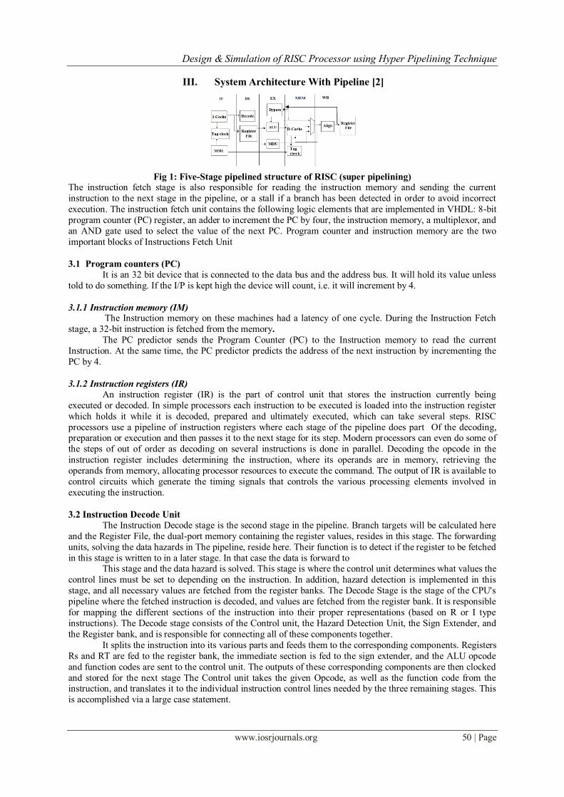
4.1 Hyper pipelining [4]
In this paper, a method is discussed that how the functionality of a core can be multiplied by adding
registers to the core. It does not only provide the less area usage compared to its individual instantiations, but it
can also provide impact on the system performance as a whole. This method is called “hyper pipelining” here
the hyper pipelined complex RISC core (OR1200 from Open Cores) is discussed. Hyper pipelining is a technique where the Core Multiplier multiplies the functionality of cores, bus-systems or complete sub designs.
It implements registers (called pipes) in the design to create CMF independent designs, whereas CMF can be
any number greater than 1. Since only registers are inserted, the resulting area is much less than duplicating the
complete design. The result is a much smaller than ASIC or lesser than FPGA size. The applied method is also
called "C-slow Retiming"
.
Fig 2: Comparison of combined 4 single RISC core with hyper pipelined RISC core with CMF=4(Core
Multiplication Factor) [4]
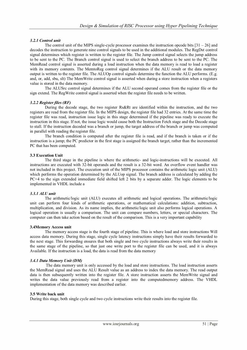
Figure 3 shows the simplified structure of sequential logic. Inputs and sequential elements clocked by clk1 drive
the combinational logic. The combinational logic drives the outputs and the data inputs of the registers. In
Figure4 each sequential element is duplicated with an intermediate register clocked by a second clock clk2. If
clk2 is synchronous to clk1, but not edge-aligned, and if the timing is right (no setup or hold time violation
between clk1 and clk2 registers), the behavior of the sequential logic doesn't change. Registers), the behavior
of the sequential logic doesn't change.
Fig 3: Simplified Sequential logic [5]
Figu4: Sequential logic with inter-logic mediate register clocked by clk2 [5]
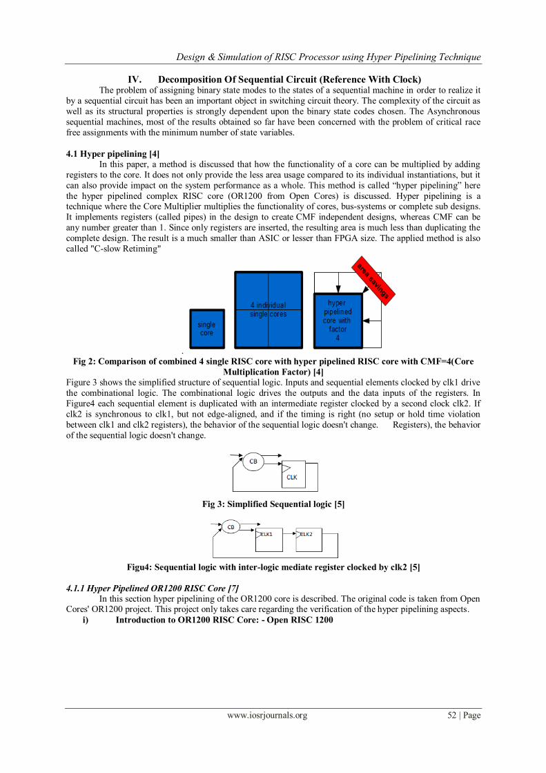
4.1.1 Hyper Pipelined OR1200 RISC Core [7]
In this section hyper pipelining of the OR1200 core is described. The original code is taken from Open Cores' OR1200 project. This project only takes care regarding the verification of the hyper pipelining aspects.
i) Introduction to OR1200 RISC Core: - Open RISC 1200
Design & Simulation of RISC Processor using Hyper Pipelining Technique
www.iosrjournals.org 53 | Page
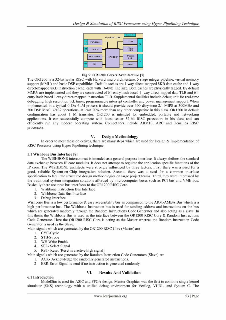
Fig 5: OR1200 Core’s Architecture [7]
The OR1200 is a 32-bit scalar RISC with Harvard micro architecture, 5 stage integer pipeline, virtual memory
support (MMU) and basic DSP capabilities. Default caches are 1-way direct-mapped 8KB data cache and 1-way
direct-mapped 8KB instruction cache, each with 16-byte line size. Both caches are physically tagged. By default
MMUs are implemented and they are constructed of 64-entry hash based 1- way direct-mpped data TLB and 64-
entry hash based 1-way direct-mapped instruction TLB. Supplemental facilities include debug unit for real-time
debugging, high resolution tick timer, programmable interrupt controller and power management support. When implemented in a typical 0.18u 6LM process it should provide over 300 dhrystone 2.1 MIPS at 300MHz and
300 DSP MAC 32x32 operations, at least 20% more than any other competitor in this class. OR1200 in default
configuration has about 1 M transistor. OR1200 is intended for embedded, portable and networking
applications. It can successfully compete with latest scalar 32-bit RISC processors in his class and can
efficiently run any modern operating system. Competitors include ARM10, ARC and Tensilica RISC
processors.
V. Design Methodology In order to meet these objectives, there are many steps which are used for Design & Implementation of
RISC Processor using Hyper Pipelining technique
5.1 Wishbone Bus Interface [8]
The WISHBONE interconnect is intended as a general purpose interface. It always defines the standard
data exchange between IP core modules. It does not attempt to regulate the application specific functions of the
IP core. The WISHBONE architects were strongly influenced by three factors. First, there was a need for a
good, reliable System-on-Chip integration solution. Second, there was a need for a common interface
specification to facilitate structured design methodologies on large project teams. Third, they were impressed by
the traditional system integration solutions afforded by microcomputer buses such as PCI bus and VME bus.
Basically there are three bus interfaces to the OR1200 RISC Core
1. Wishbone Instruction Bus Interface
2. Wishbone Data Bus Interface 3. Debug Interface
Wishbone Bus is a low performance & easy accessibility bus as comparison to the ARM-AMBA Bus which is a
high performance bus. The Wishbone Instruction bus is used for sending address and instructions on the bus
which are generated randomly through the Random Instructions Code Generator and also acting as a slave. In
this thesis the Wishbone Bus is used as the interface between the OR1200 RISC Core & Random Instructions
Code Generator. Here the OR1200 RISC Core is acting as the Master whereas the Random Instruction Code
Generator is used as the Slave.
Main signals which are generated by the OR1200 RISC Core (Master) are
1. CYC-Cycle
2. STB-Strobe
3. WE-Write Enable 4. SEL- Select Signal
5. RST- Reset (Reset is a active high signal).
Main signals which are generated by the Random Instruction Code Generators (Slave) are
1. ACK- Acknowledge the randomly generated instructions.
2 ERR-Error Signal is send if no instruction is generated randomly.
VI. Results And Validation 6.1 Introduction
ModelSim is used for ASIC and FPGA design. Mentor Graphics was the first to combine single kernel simulator (SKS) technology with a unified debug environment for Verilog, VHDL, and System C. The
Design & Simulation of RISC Processor using Hyper Pipelining Technique
www.iosrjournals.org 54 | Page
combination of industry-leading, native SKS performance with the best integrated debug and analysis
environment make ModelSim the simulator of choice for both ASIC and FPGA designs. The best standards and
platform support in the industry make it easy to adopt in the majority of process and tool flows.
6.2 Database for Compilation & Simulation: -
ModelSimcombines simulation performance and capacity with the code coverage and debugging
capabilities required to simulate multiple blocks and systems and attain ASIC gate-level sign-off.
Comprehensive support of Verilog, SystemVerilog for Design, VHDL, and SystemC provide a solid foundation
for single and multi-language design verification environments. ModelSim’s easy to use and unified debug and
simulation environment provide today’s FPGA designers both the advanced capabilities that they are growing to
need and the environment that makes their work productive.
6.2.1Different steps for Compiling a Design
1. Code Your Design
2. Start ModelSim 3. Set the Working Directory
4. Create a Work library
5. Compile a Design
6.2.2 Different steps for Simulating a Design
1. Code the Testbench
2. Compile the Testbench
3. Load the Testbench
4. Display Waveforms
5. Run the Simulation
6. Recompiling and Rerunning a Simulation
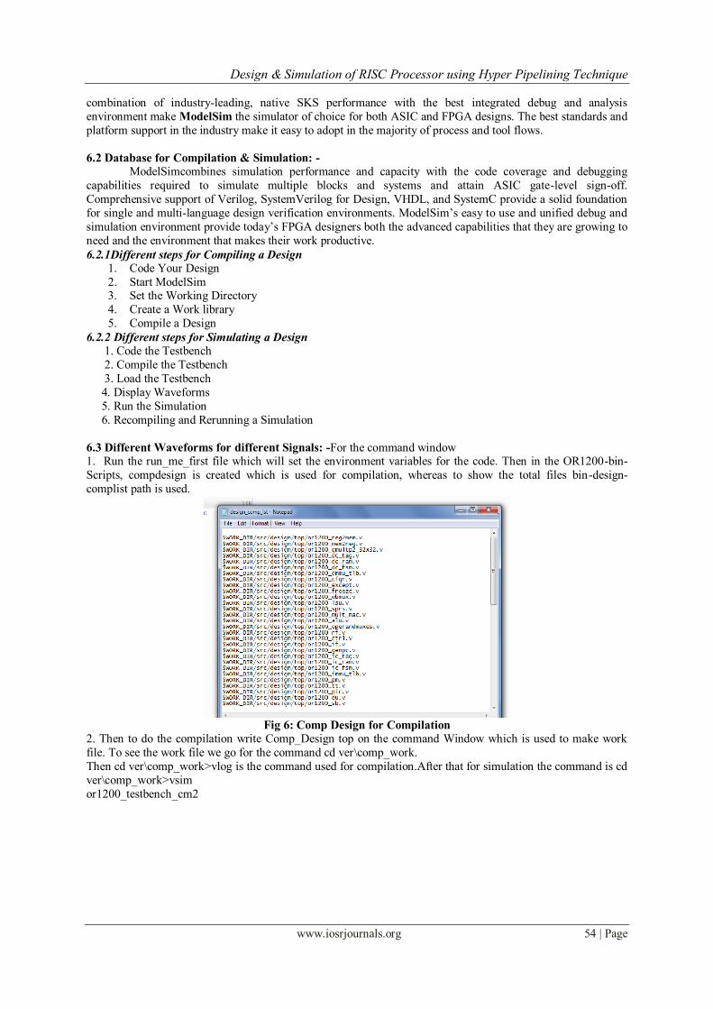
6.3 Different Waveforms for different Signals: -For the command window 1. Run the run_me_first file which will set the environment variables for the code. Then in the OR1200-bin-
Scripts, compdesign is created which is used for compilation, whereas to show the total files bin-design-
complist path is used.
Fig 6: Comp Design for Compilation
2. Then to do the compilation write Comp_Design top on the command Window which is used to make work
file. To see the work file we go for the command cd ver\comp_work.
Then cd ver\comp_work>vlog is the command used for compilation.After that for simulation the command is cd
ver\comp_work>vsim
or1200_testbench_cm2
Design & Simulation of RISC Processor using Hyper Pipelining Technique
www.iosrjournals.org 55 | Page
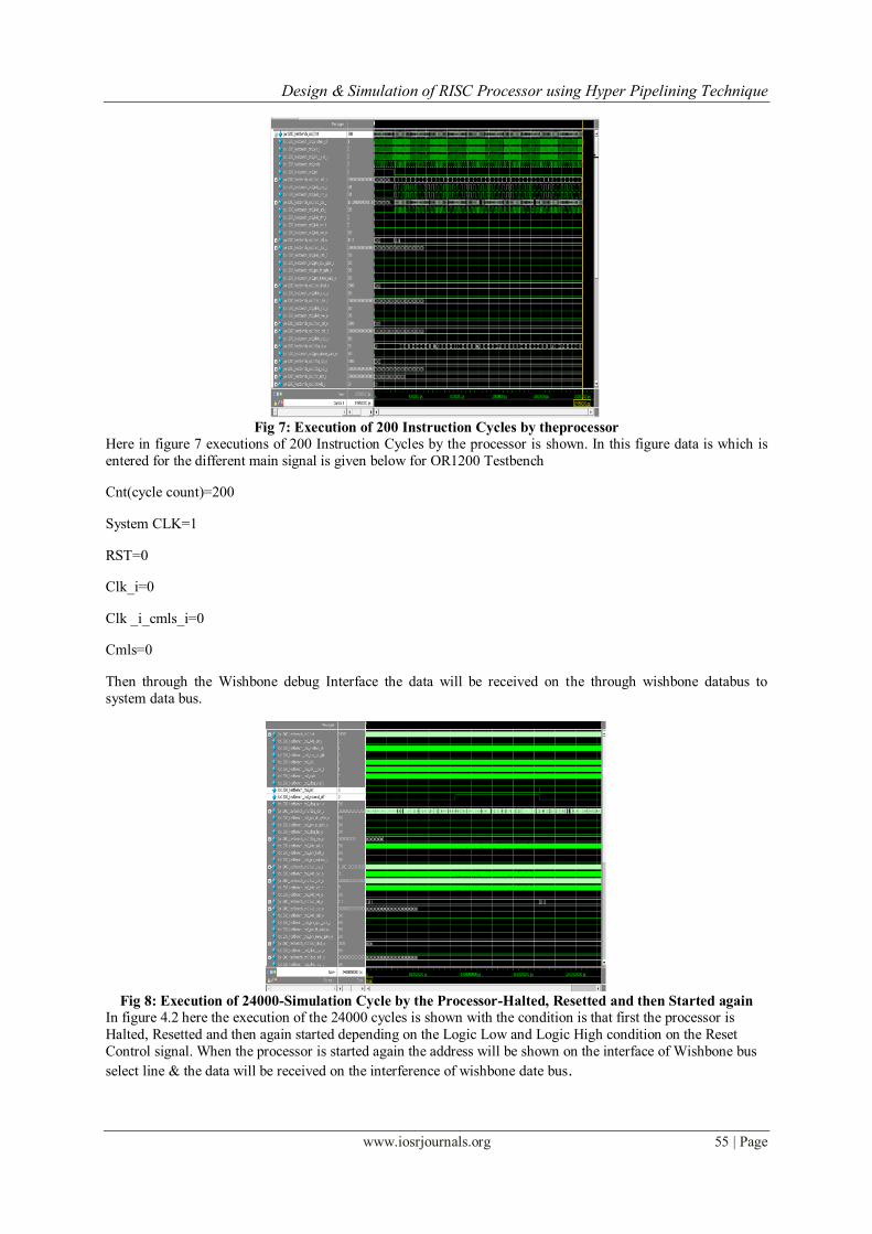
Fig 7: Execution of 200 Instruction Cycles by theprocessor
Here in figure 7 executions of 200 Instruction Cycles by the processor is shown. In this figure data is which is
entered for the different main signal is given below for OR1200 Testbench
Cnt(cycle count)=200
System CLK=1
RST=0
Clk_i=0
Clk _i_cmls_i=0
Cmls=0
Then through the Wishbone debug Interface the data will be received on the through wishbone databus to
system data bus.
Fig 8: Execution of 24000-Simulation Cycle by the Processor-Halted, Resetted and then Started again
In figure 4.2 here the execution of the 24000 cycles is shown with the condition is that first the processor is
Halted, Resetted and then again started depending on the Logic Low and Logic High condition on the Reset
Control signal. When the processor is started again the address will be shown on the interface of Wishbone bus
select line & the data will be received on the interference of wishbone date bus.
Design & Simulation of RISC Processor using Hyper Pipelining Technique
www.iosrjournals.org 56 | Page
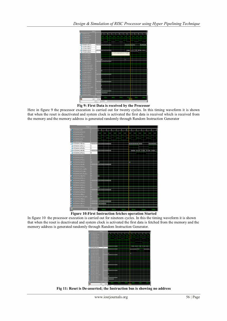
Fig 9: First Data is received by the Processor
Here in figure 9 the processor execution is carried out for twenty cycles. In this timing waveform it is shown
that when the reset is deactivated and system clock is activated the first data is received which is received from
the memory and the memory address is generated randomly through Random Instruction Generator
Figure 10:First Instruction fetches operation Started
In figure 10 the processor execution is carried out for nineteen cycles. In this the timing waveform it is shown
that when the reset is deactivated and system clock is activated the first data is fetched from the memory and the
memory address is generated randomly through Random Instruction Generator.
Fig 11: Reset is De-asserted; the Instruction bus is showing no address
Design & Simulation of RISC Processor using Hyper Pipelining Technique
www.iosrjournals.org 57 | Page
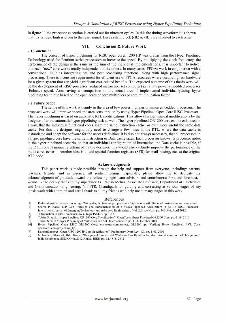
In figure 11 the processor execution is carried out for nineteen cycles. In this the timing waveform it is shown
that firstly logic high is given to the reset signal. Here system clock (clk) & clk_i are inverted to each other.
VII. Conclusion & Future Work 7.1 Conclusion
The concept of hyper pipelining for RISC open cores 1200 HP was drawn from the Hyper Pipelined
Technology used for Pentium series processors to increase the speed. By multiplying the clock frequency, the
performance of the design is the same as the sum of the individual implementations. It is important to notice,
that each "new" core works totally independent of the others. In many cases, FPGAs work in conjunction with a
conventional DSP as integrating pre and post processing functions, along with high performance signal
processing. There is a constant requirement for efficient use of FPGA resources where occupying less hardware
for a given system that can yield significant cost-related benefits. The expected outcome of this thesis work will be the development of RISC processor (reduced instruction set computer) i.e. a low power embedded processor
-Enhance speed, Area saving as comparison to the actual area if implemented individuallyUsing hyper
pipelining technique based on the open cores or core multipliers or core multiplication factor.
7.2 Future Scope The scope of this work is mainly in the area of low power high performance embedded processors. The
proposed work will improve speed and area consumption by using Hyper Pipelined Open Core RISC Processor.
The hyper pipelining is based on automatic RTL modifications. This allows further manual modifications by the
designer after the automatic hyper pipelining task as well. The hyper pipelined OR1200 core can be enhanced in
a way, that the individual functional cores share the same instruction cache or even more useful the same data
cache. For this the designer might only need to change a few lines in the RTL, where the data cache is
instantiated and adopt the software for the access definition. It is also not always necessary, that all processors in
a hyper pipelined core have the same Instruction or Data cache sizes. Each processor knows its processor index
in the hyper pipelined scenario, so that an individual configuration of Instruction and Data cache is possible, if
the RTL code is manually enhanced by the designer, this would also certainly improve the performance of the
multi core scenario. Another idea is to add special function registers (SFR) for mail-boxing, etc. to the original RTL code.
Acknowledgments This paper work is made possible through the help and support from everyone, including: parents,
teachers, friends, and in essence, all sentient beings. Especially, please allow me to dedicate my
acknowledgment of gratitude toward the following significant advisors and contributors: First and foremost, I
would like to deeply thank to my supervisor Er. Rajesh Mehra, Associate Professor, Department of Electronics
and Communication Engineering, NITTTR, Chandigarh for guiding and correcting at various stages of my
thesis work with attention and care.I thank to all my friends who help me at many stages in this work.
References [1] Reduced instruction set computing - Wikipedia, the free encyclopediaen.wikipedia.org/ wiki/Reduced_instruction_set_computing.
[2] Sharda P. Katke, G.P. Jain “Design and Implementation of 5 Stages Pipelined Architecture in 32 Bit RISC Processor”,
International Journal of Emerging Technology and Advanced Engineering , Vol. 2, Issue No.4, pp. 340-346, April 2012.
[3] Introduction to RISC Processors by ni logic Pvt.Ltd, pp. 1-42
[4] Tobias Strauch, “Hyper Pipelined OR1200 Core Specification”, OpenCores Hyper Pipelined OR1200 Core, pp.-1-19, 2010
[5] Tobias Strauch “Hyper Pipelining of Multicores and SoC Interconnects”, pp. 1-16, October 2010
[6] Hyper Pipelined Open RISC OR1200 Core, opencores.com/project, OR1200_hp, (Verilog) Hyper Pipelined AVR Core,
opencores.com/project,avr_hp,
[7] DamjanLampret “Open RISC 1200 IP Core Specification”, Preliminary Draft Rev.-0.7, pp.-1-63, 2001
[8] Mohandeep Sharma1, Dilip Kumar “Design and Synthesis of Wishbone Bus Dataflow Interface Architecture for SoC Integration”,
India Conference (INDICON), 2012 Annual IEEE, pp.-813-818, 2012