Embed Size (px)
Citation preview
Dr A SahuDept of Computer Science &
Engineering IIT Guwahati

• Programmable Interface device (Introduction)
• Requirement for programmable interface device
• Simple example configurable device
• Programmable Interface device 8155– Block diagram
– Address diagram
– Interfacing LED using 8155
• 8155 Timer – Modes of timer
– Square wave generation using 8155 interfaced timer
• Next class (8055 Handshake & Interrupt mode)

• Designed to perform various I/O functions
• Device can be setup to perform specific functions
– By writing instruction to a internal register
• Can be changed during execution of the program
• Devices are flexible, versatile & economical

• Functions are determined by software instructions
• Can be viewed as multiple I/O device
• Perform many functions– Time delay, counting, interrupts
• Consists of many devices on a chip, interconnect through a common Bus
• Software programmable approach of I/O reduce design time

• I/P & O/P Regs: A group of latches to hold data
• Tri-State Buffer
• Capability of Bidirectional data flow
• Handshake & Interrupt signal
• Control Logic
• Chip Select Logic
• Interrupt control logic

• Configurable Device Example
• Latch Direction
A
B
Direction Chip Select

• ProgramMVI A,01 H ; Set Do=1, D1-D7==0OUT FFH ;Write in control registerMVI A,BYTE1 ;Load data byeOUT FEH ; Send Data out
7A
0A
DIRG: Enable
7B
0B
Control Reg
D0D1
D7A7A6A5A4A3A2A1
A0

• 2kbits static RAM 256x8
• 2 programmable 8 bit I/O ports
• 1 programmable 6 bit I/O port
• 1 programmable 14 bit binary counter/timer
• Internal address latch to Demux AD0-AD7, using ALE line
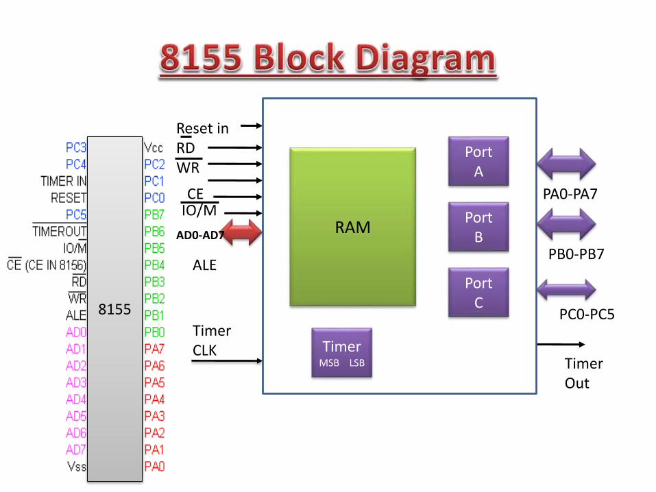
RAM
PortA
PortB
PortC
TimerMSB LSB
PA0-PA7
PB0-PB7
PC0-PC5
Timer Out
Reset inRDWR
ALE
CEIO/M
AD0-AD7
8155
Timer CLK

3 to 8 Decoder
CWR
PortA
PortB
PortC
TimerMSB LSB
Latch
Clock for timer
PA0-PA7
PB0-PB7
PC0-PC5
Timer Out
A0
A1
A2ALE
AD0-AD7A0-A7
D7-D0
012345
CEb
A2 A1 A0 Port (ALE high, AD0=A0)
0 0 0 Command/Status Register
0 0 1 PA
0 1 0 PB
0 1 1 PC
1 0 0 Timer LSB
1 0 1 Timer MSB

3 to 8 Decoder
04A13A12A11
A15A14
A2A1A0
5V
3 to 8 Decoder
RAM
Control
CWR
PortA
PortB
PortC
TimerMSB LSB
Latch
Clock for timer
PA0-PA7
PB0-PB7
PC0-PC5
Timer Out
Reset inRDWR
A0
A1
A2
ALE
CE
IO/M
IO/M
AD0-AD7
A0-A7
D7-D0
20H
21H
22H
23H
24H
25H
CS

3 to 8 Decoder
RAM
Control
CWR
PortA
PortB
PortC
TimerMSB LSB
Latch
Clock for timer
PA0-PA7
PB0-PB7
PC0-PC5
Timer Out
Reset inRDWR
A0
A1
A2
ALE
CEIO/M
IO/M
AD0-AD7
A0-A7
D7-D08155
20H
21H
22H
23H
24H
25H

• D0, D1: mode for PA and PB, 0=IN, 1=OUT
• D2, D3: mode for PC
• D4, D5: interrupt EN for PA and PB, 0=disable 1=enable
• D6, D7: Timer command: – 00: No effect
– 01: Stop if running else no effect
– 10: Stop after terminal count (TC) if running, else no effect
– 11: Start if not running, reload at TC if running.
• Port C bits
(D2, D3)
D7 D6 D5 D4 D3 D2 D1 D0
Timer Command IEB IEA PC PB PA
ALT D3 D2 PC5 PC4 PC3 PC2 PC1 PC0
1 0 0 IN IN IN IN IN IN
2 0 1 OUT OUT OUT OUT OUT OUT
3 1 0 OUT OUT OUT STBA BFA INTRA
4 1 1 STBB BFB INTRB STBA BFA INTRA

8155
PA7PA6PA5PA4
PA3PA2PA1PA0
PB7PB6PB5PB4
PB3PB2PB1PB0
AD7to
AD0
IO/Mb
ALERDb
WRb
RESET OUT
IO/Mb
ALERDb
WRb
RESET OUT
7 SegLED
Driver
7 SegLED
Driver
7 SegLED
Driver
7 SegLED
Driver
3 to 8 Decoder
04A13A12A11
A15A14
A2A1A0
5V

• Port Address– Control Register=20H, Port A= 21H, Port B= 22H
• Control word:
• Program– MVI A,03 ; initialize Port A &B for O/P– OUT 20H– MVI A, BYTE1 ; Display BYTE1 at port A– OUT 21H– MVI A, BYTE2 ; Display BYTE2 at port B– OUT 22H
D7 D6 D5 D4 D3 D2 D1 D0
0 0 0 0 0 0 1 1
Timer NotApplicable
Use for Port C
Port BOutput
Port AOutput

• R S Gaonkar, “Microprocessor Architecture”, Chapter 14


![Ep118 Lec11 Optoelectronics[1]](https://img.pdfslide.net/doc/110x75/563db867550346aa9a93659b/ep118-lec11-optoelectronics1.jpg)