Embed Size (px)
Citation preview
Engr.Tehseen Ahsan
Lecturer, Electrical Engineering Department
EE-307 Electronic Systems Design
HITEC University Taxila Cantt, Pakistan
The Operational Amplifier (Part 1)
12-1 Introduction to Operational Amplifiers The devices, such as diode and the transistor, are separate
devices that are individually packaged and interconnected in a
circuit with other devices to form a complete, functional
unit- Discrete Components.
Linear integrated circuits (ICs), where many transistors, diodes,
resistors and capacitors are fabricated on a single tiny chip of
semiconductor material.
This means that we will be concerned with what the circuit
does from an external view point than from an internal,
component-level viewpoint.
2
12-1 Introduction to Operational Amplifiers Continue…
Early operational Amplifiers ( i.e, used for +,-, ∫ and d/dx).
Early op-amp were constructed with vaccum tubes and
worked with high voltages.
Today’s op-amp are linear ICs that use relatively low dc
supply voltages and are reliable and inexpensive.
3
12-1 Introduction to Operational Amplifiers Continue…
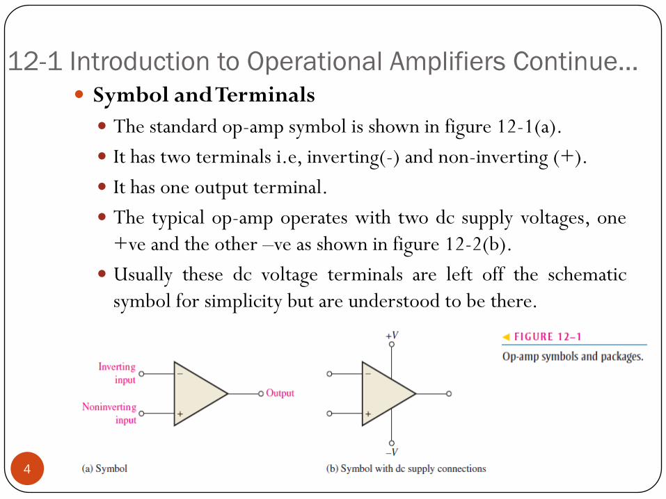
Symbol andTerminals
The standard op-amp symbol is shown in figure 12-1(a).
It has two terminals i.e, inverting(-) and non-inverting (+).
It has one output terminal.
The typical op-amp operates with two dc supply voltages, one
+ve and the other –ve as shown in figure 12-2(b).
Usually these dc voltage terminals are left off the schematic
symbol for simplicity but are understood to be there.
4
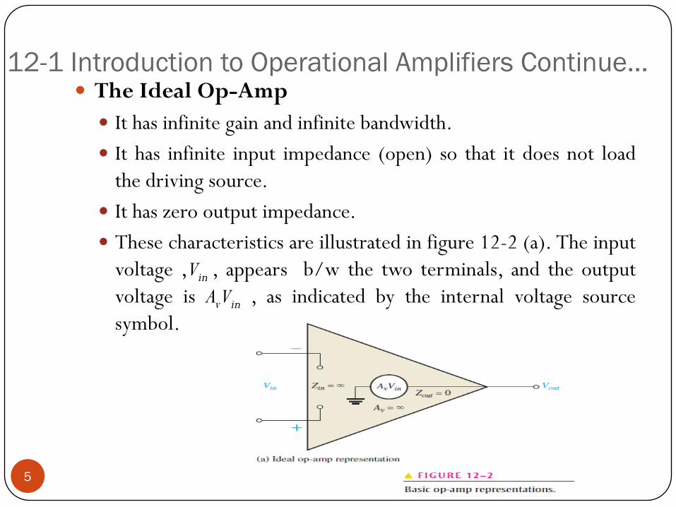
12-1 Introduction to Operational Amplifiers Continue… The Ideal Op-Amp
It has infinite gain and infinite bandwidth.
It has infinite input impedance (open) so that it does not load
the driving source.
It has zero output impedance.
These characteristics are illustrated in figure 12-2 (a). The input
voltage ,Vin , appears b/w the two terminals, and the output
voltage is AvVin , as indicated by the internal voltage source
symbol.
5
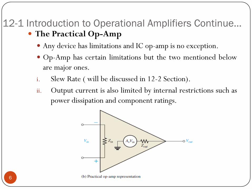
12-1 Introduction to Operational Amplifiers Continue… The Practical Op-Amp
Any device has limitations and IC op-amp is no exception.
Op-Amp has certain limitations but the two mentioned below
are major ones.
i. Slew Rate ( will be discussed in 12-2 Section).
ii. Output current is also limited by internal restrictions such as
power dissipation and component ratings.
6
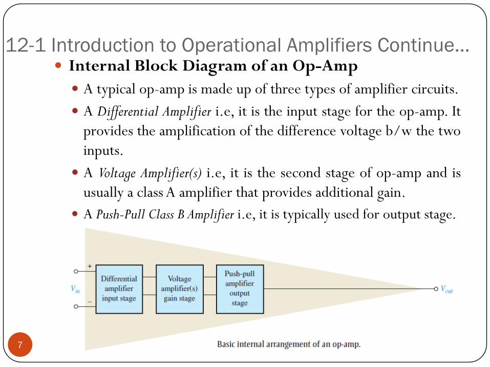
12-1 Introduction to Operational Amplifiers Continue… Internal Block Diagram of an Op-Amp
A typical op-amp is made up of three types of amplifier circuits.
A Differential Amplifier i.e, it is the input stage for the op-amp. It
provides the amplification of the difference voltage b/w the two
inputs.
A Voltage Amplifier(s) i.e, it is the second stage of op-amp and is
usually a class A amplifier that provides additional gain.
A Push-Pull Class B Amplifier i.e, it is typically used for output stage.
7
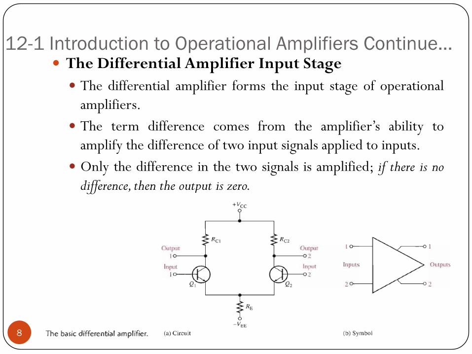
12-1 Introduction to Operational Amplifiers Continue… The Differential Amplifier Input Stage
The differential amplifier forms the input stage of operational
amplifiers.
The term difference comes from the amplifier’s ability to
amplify the difference of two input signals applied to inputs.
Only the difference in the two signals is amplified; if there is no
difference, then the output is zero.
8
12-1 Introduction to Operational Amplifiers Continue… The Differential Amplifier Input Stage Continue…
The transistors (Q1 and Q2) and the collector resistors (RC1 and
RC2) are carefully matched to have identical characteristics
(Refer to figure in previous slide).
Notice that the two transistors share a single RE.
Let us suppose both bases are connected to ground. The emitter
voltage will be -0.7V .
The emitter currents are equal (IE1= IE2).
The collector currents are both equal and are approximately
equal to the emitter currents.
Since collector currents are the same, the collector voltages are
also the same.
There is a zero difference in the input voltages ( both bases are
at 0V).9
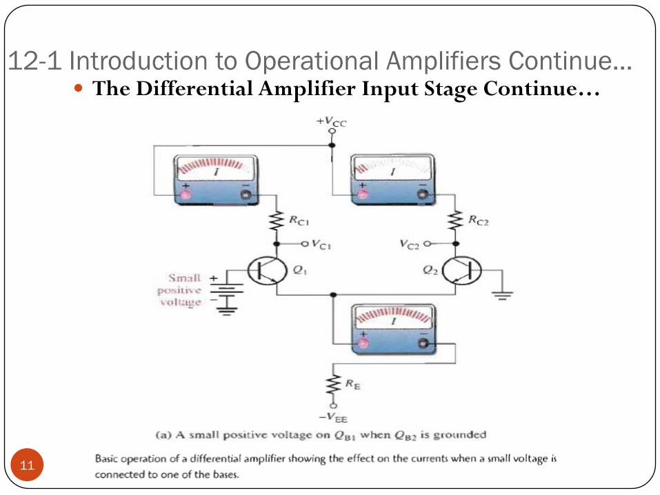
12-1 Introduction to Operational Amplifiers Continue… The Differential Amplifier Input Stage Continue…
If the base of Q1 is disconnected from ground and connected to
a small positive voltage, Q1 will conduct more current because
the positive voltage on its base causes the emitter voltage to
increase slightly.
The emitter current is now divided so that more of it is in Q1and less in Q2.
As a result the collector voltage of Q1 will decrease and the
collector voltage of Q2 will increase, reflecting the difference in
the input voltages (one is 0 V and the other at a small positive
value).
This condition is illustrated in figure next slide.
10
12-1 Introduction to Operational Amplifiers Continue… The Differential Amplifier Input Stage Continue…
11
12-2 OP-AMP Input Modes and Parameters
The differential amplifier exhibits three modes of
operation based on the type of input signals. These
modes are single-ended, differential and common. Since
the differential amplifier is the input stage of the op-
amp, the op-amp exhibits the same modes.
12
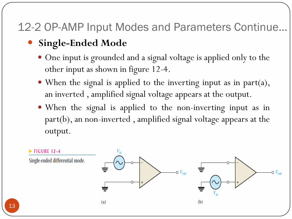
12-2 OP-AMP Input Modes and Parameters Continue…
Single-Ended Mode
One input is grounded and a signal voltage is applied only to the
other input as shown in figure 12-4.
When the signal is applied to the inverting input as in part(a),
an inverted , amplified signal voltage appears at the output.
When the signal is applied to the non-inverting input as in
part(b), an non-inverted , amplified signal voltage appears at the
output.
13
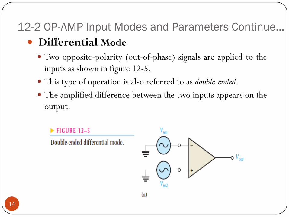
12-2 OP-AMP Input Modes and Parameters Continue…
DifferentialMode Two opposite-polarity (out-of-phase) signals are applied to the
inputs as shown in figure 12-5.
This type of operation is also referred to as double-ended.
The amplified difference between the two inputs appears on the
output.
14
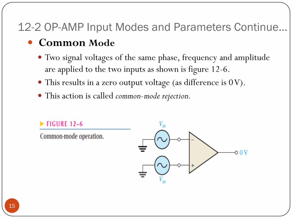
12-2 OP-AMP Input Modes and Parameters Continue…
CommonMode Two signal voltages of the same phase, frequency and amplitude
are applied to the two inputs as shown is figure 12-6.
This results in a zero output voltage (as difference is 0V).
This action is called common-mode rejection.
15
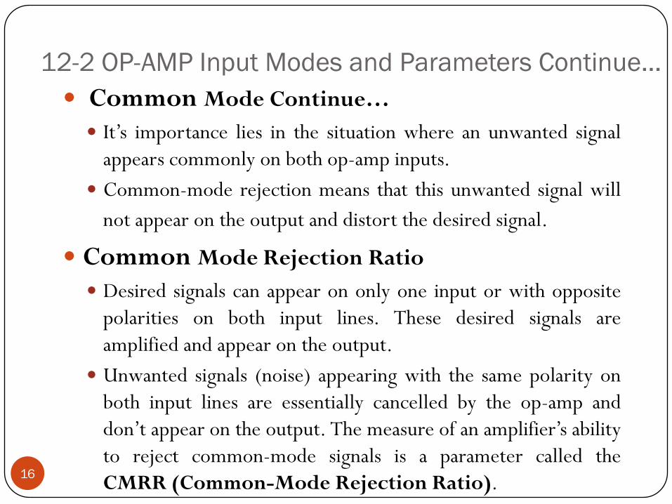
12-2 OP-AMP Input Modes and Parameters Continue…
CommonMode Continue… It’s importance lies in the situation where an unwanted signal
appears commonly on both op-amp inputs.
Common-mode rejection means that this unwanted signal will
not appear on the output and distort the desired signal.
CommonMode Rejection Ratio
Desired signals can appear on only one input or with opposite
polarities on both input lines. These desired signals are
amplified and appear on the output.
Unwanted signals (noise) appearing with the same polarity on
both input lines are essentially cancelled by the op-amp and
don’t appear on the output. The measure of an amplifier’s ability
to reject common-mode signals is a parameter called the
CMRR (Common-Mode Rejection Ratio).16
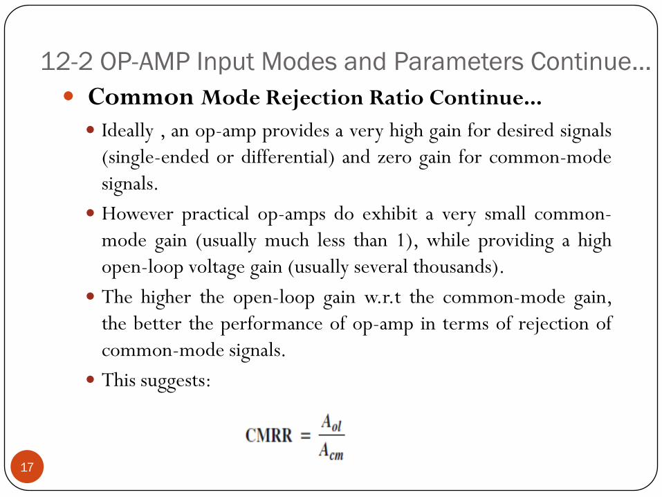
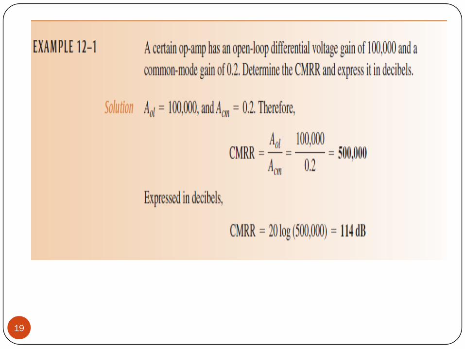
12-2 OP-AMP Input Modes and Parameters Continue…
CommonMode Rejection Ratio Continue... Ideally , an op-amp provides a very high gain for desired signals
(single-ended or differential) and zero gain for common-mode
signals.
However practical op-amps do exhibit a very small common-
mode gain (usually much less than 1), while providing a high
open-loop voltage gain (usually several thousands).
The higher the open-loop gain w.r.t the common-mode gain,
the better the performance of op-amp in terms of rejection of
common-mode signals.
This suggests:
17
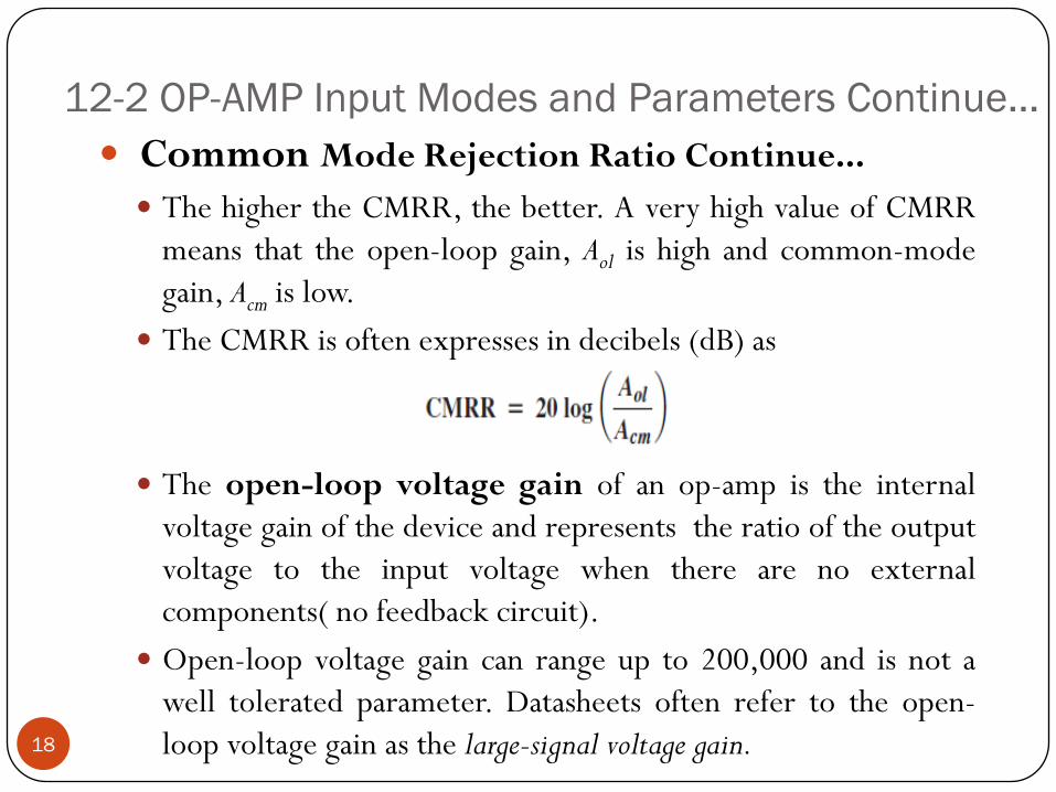
12-2 OP-AMP Input Modes and Parameters Continue…
CommonMode Rejection Ratio Continue... The higher the CMRR, the better. A very high value of CMRR
means that the open-loop gain, Aol is high and common-mode
gain, Acm is low.
The CMRR is often expresses in decibels (dB) as
The open-loop voltage gain of an op-amp is the internal
voltage gain of the device and represents the ratio of the output
voltage to the input voltage when there are no external
components( no feedback circuit).
Open-loop voltage gain can range up to 200,000 and is not a
well tolerated parameter. Datasheets often refer to the open-
loop voltage gain as the large-signal voltage gain.18
19
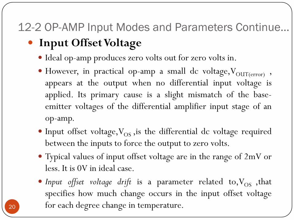
12-2 OP-AMP Input Modes and Parameters Continue…
Input OffsetVoltage Ideal op-amp produces zero volts out for zero volts in.
However, in practical op-amp a small dc voltage,VOUT(error) ,
appears at the output when no differential input voltage is
applied. Its primary cause is a slight mismatch of the base-
emitter voltages of the differential amplifier input stage of an
op-amp.
Input offset voltage,VOS ,is the differential dc voltage required
between the inputs to force the output to zero volts.
Typical values of input offset voltage are in the range of 2mV or
less. It is 0V in ideal case.
Input offset voltage drift is a parameter related to,VOS ,that
specifies how much change occurs in the input offset voltage
for each degree change in temperature.20
12-2 OP-AMP Input Modes and Parameters Continue…
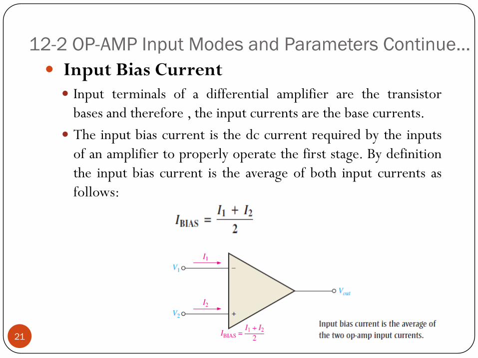
Input Bias Current Input terminals of a differential amplifier are the transistor
bases and therefore , the input currents are the base currents.
The input bias current is the dc current required by the inputs
of an amplifier to properly operate the first stage. By definition
the input bias current is the average of both input currents as
follows:
21
12-2 OP-AMP Input Modes and Parameters Continue…
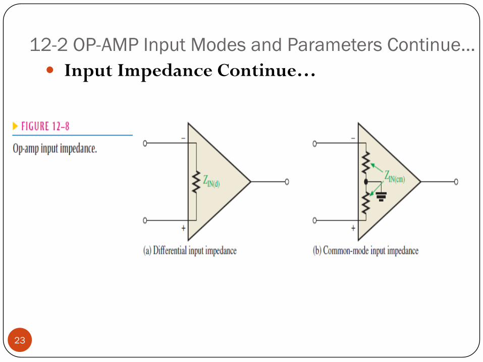
Input Impedance Two basic ways of specifying the input impedance
1. The Differential input impedance is the total resistance between
the inverting and non-inverting terminals as illustrated 12-8
(a) next slide. Differential impedance is measured by
determining the change in bias current for a given change in
differential input voltage.
2. The common-mode input impedance is the resistance between
each input and ground and is measured by determining the
change in bias current for a given change in common-mode
input voltage shown in figure 12-8(b) next slide .
22
12-2 OP-AMP Input Modes and Parameters Continue…
Input Impedance Continue…
23
12-2 OP-AMP Input Modes and Parameters Continue…
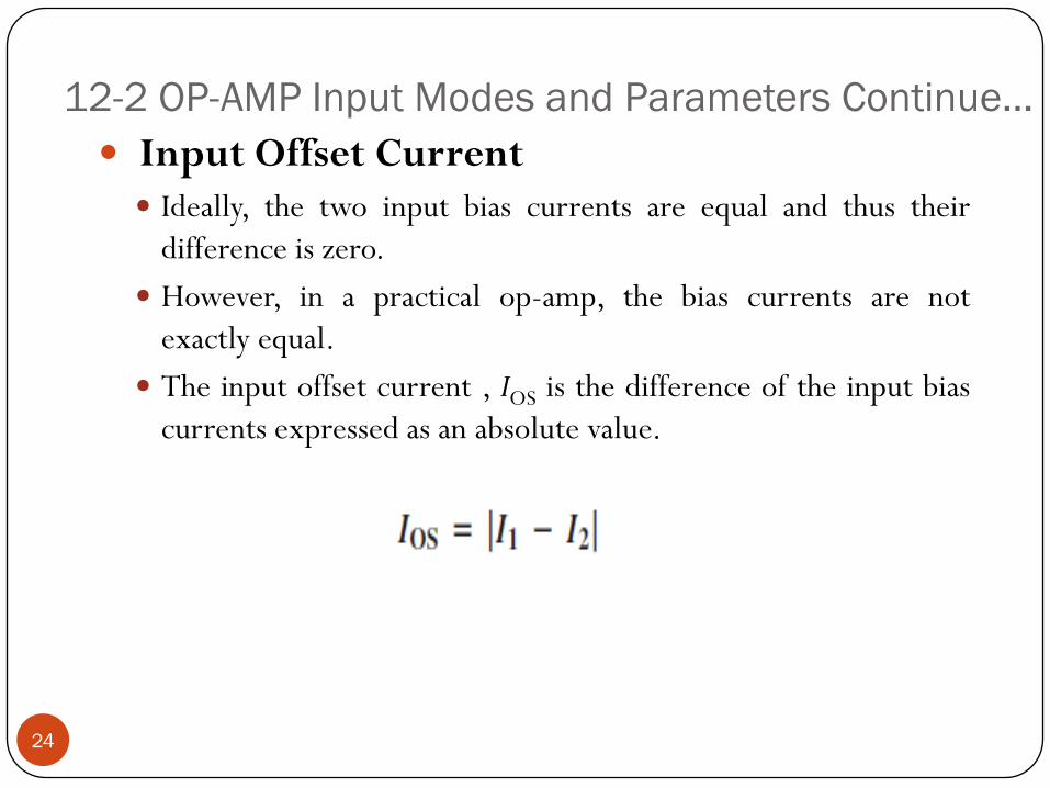
Input Offset Current Ideally, the two input bias currents are equal and thus their
difference is zero.
However, in a practical op-amp, the bias currents are not
exactly equal.
The input offset current , IOS is the difference of the input bias
currents expressed as an absolute value.
24
12-2 OP-AMP Input Modes and Parameters Continue…
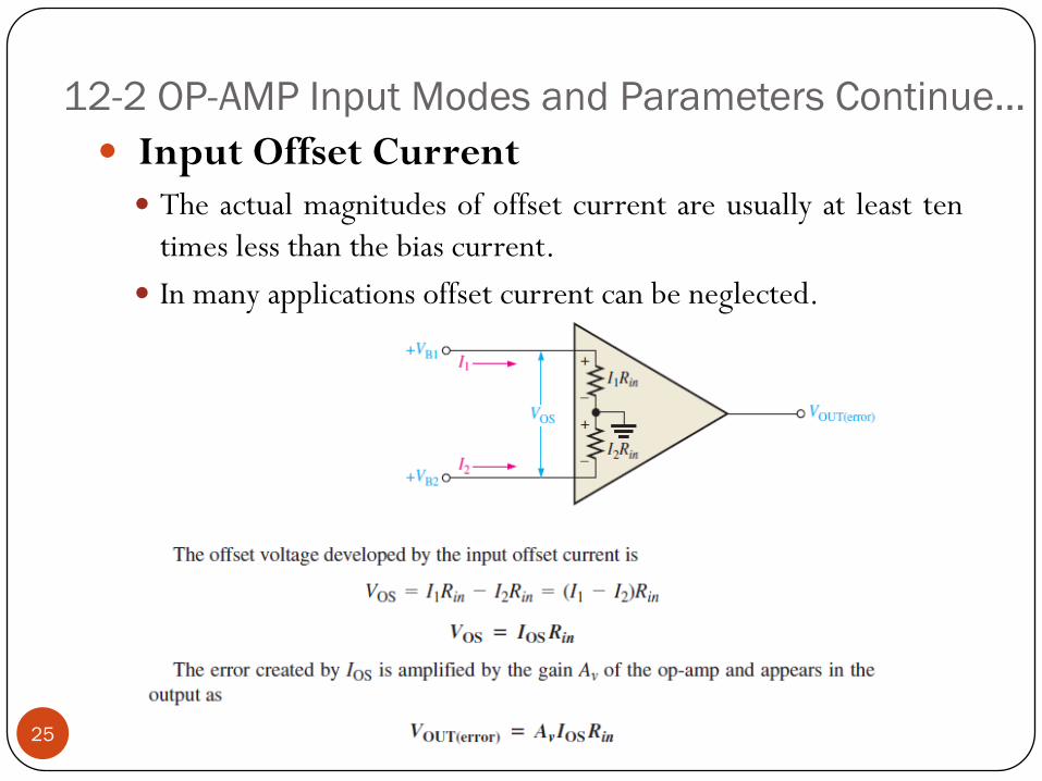
Input Offset Current The actual magnitudes of offset current are usually at least ten
times less than the bias current.
In many applications offset current can be neglected.
25
12-2 OP-AMP Input Modes and Parameters Continue…
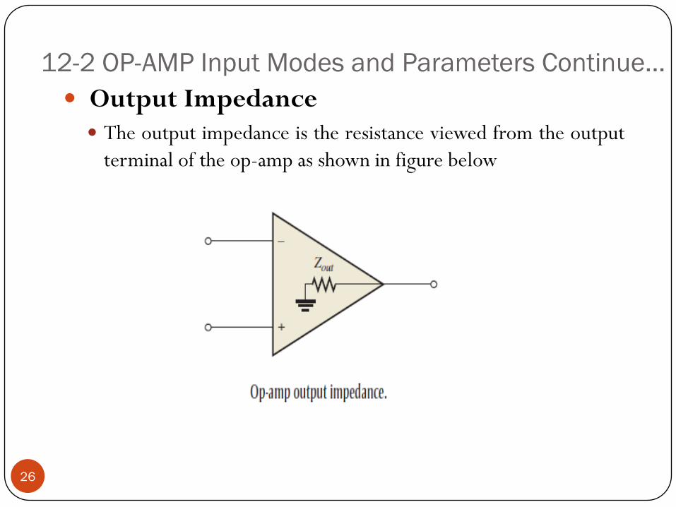
Output Impedance The output impedance is the resistance viewed from the output
terminal of the op-amp as shown in figure below
26
12-2 OP-AMP Input Modes and Parameters Continue…
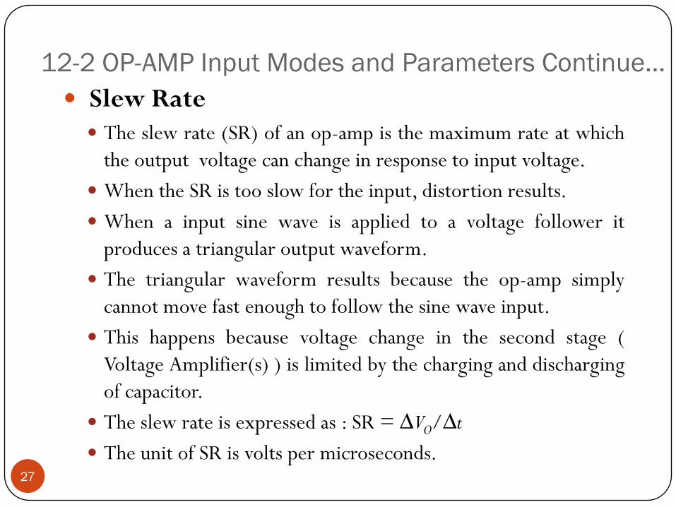
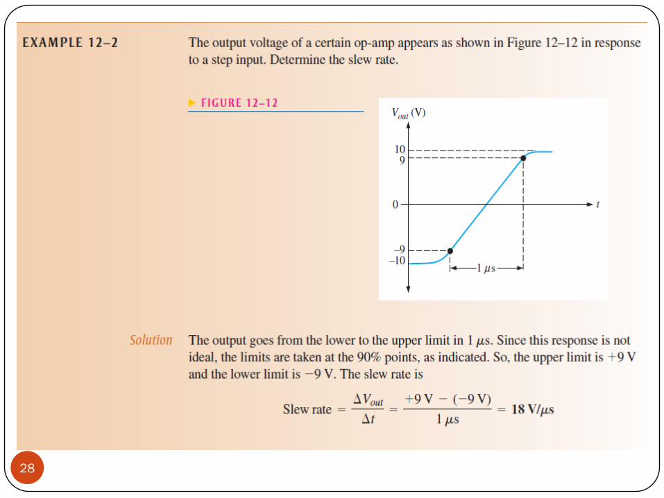
Slew Rate The slew rate (SR) of an op-amp is the maximum rate at which
the output voltage can change in response to input voltage.
When the SR is too slow for the input, distortion results.
When a input sine wave is applied to a voltage follower it
produces a triangular output waveform.
The triangular waveform results because the op-amp simply
cannot move fast enough to follow the sine wave input.
This happens because voltage change in the second stage (
Voltage Amplifier(s) ) is limited by the charging and discharging
of capacitor.
The slew rate is expressed as : SR = ∆VO/∆t
The unit of SR is volts per microseconds.27
28
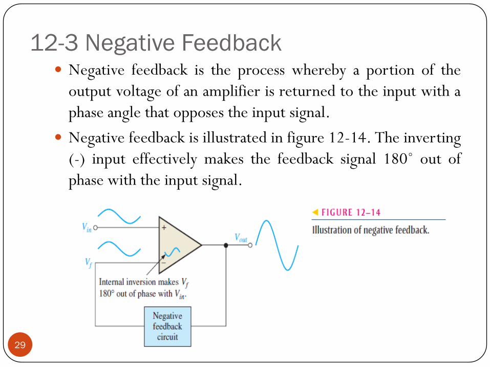
12-3 Negative Feedback Negative feedback is the process whereby a portion of the
output voltage of an amplifier is returned to the input with a
phase angle that opposes the input signal.
Negative feedback is illustrated in figure 12-14. The inverting
(-) input effectively makes the feedback signal 180˚ out of
phase with the input signal.
29
12-3 Negative Feedback Why Use Negative Feedback?
The inherent open-loop voltage gain of a typical op-amp is very
high ( usually greater than 100,000). Therefore , an extremely
small input voltage drives the op-amp into its saturated output
states. In fact , even the input offset voltage of an op-amp can
drive it into saturation. For example, assume VIN= 1 mV and Aol= 100,000.Then, Vout= VIN Aol= 100V
Since the output level of an op-amp can never reach 100 V, it is
driven deep into saturation and the output is limited to its
maximum output levels as illustrated in figure 12-15 next slide
for both a positive and negative input voltage of 1 mV.
30
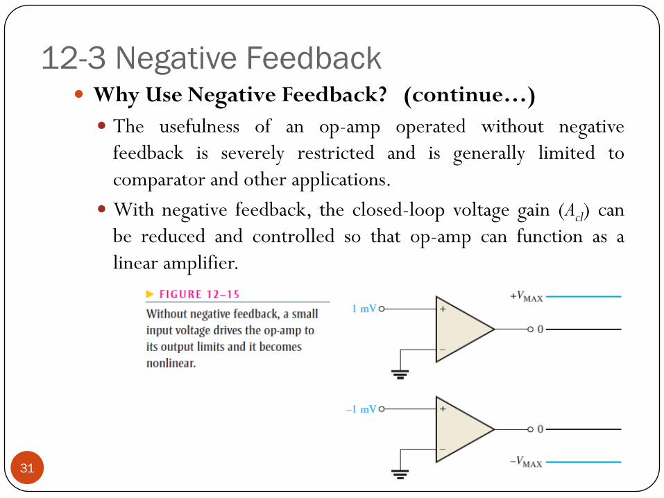
12-3 Negative Feedback Why Use Negative Feedback? (continue…)
The usefulness of an op-amp operated without negative
feedback is severely restricted and is generally limited to
comparator and other applications.
With negative feedback, the closed-loop voltage gain (Acl) can
be reduced and controlled so that op-amp can function as a
linear amplifier.
31
12-4 OP-AMPS With Negative Feedback The extremely high open-loop gain of an op-amp creates an
unstable situation because a small noise voltage on the input
can be amplified to a point where the amplifier is driven out
of its linear region.
Negative feedback takes a portion of the output and applies it
back out of phase with the input, creating an effective
reduction in gain.
This closed-loop gain is usually much less than the open-loop
gain.
32
12-4 OP-AMPS With Negative Feedback Continue… Closed-LoopVoltage Gain, Acl The closed-loop gain is the voltage gain of an op-amp with
external feedback. The amplifier configuration consists of the
op-amp and an external feedback circuit that connects the
output to inverting input.
The closed-loop voltage gain is determined by the external
component values and can be precisely controlled by them.
33
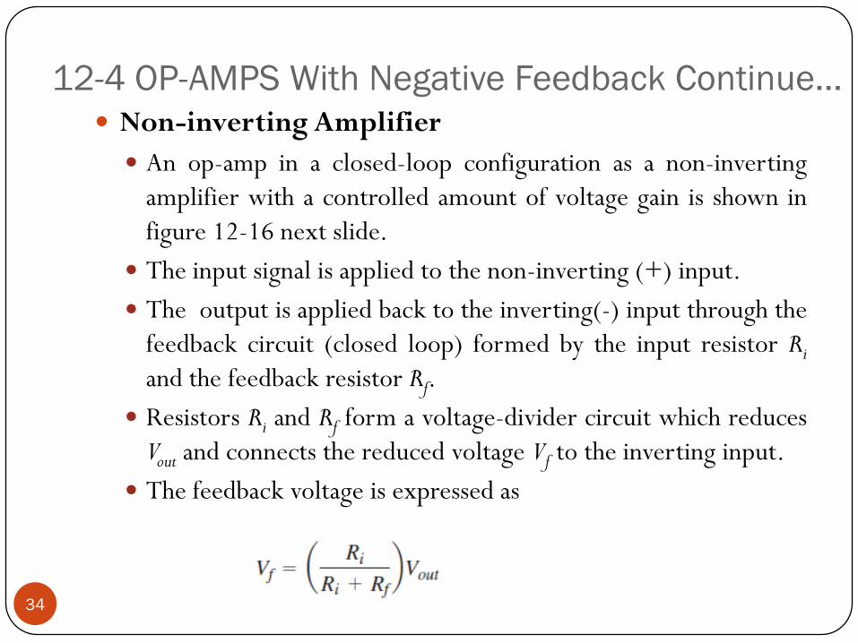
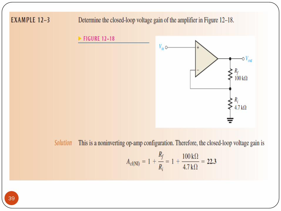
12-4 OP-AMPS With Negative Feedback Continue… Non-inverting Amplifier
An op-amp in a closed-loop configuration as a non-inverting
amplifier with a controlled amount of voltage gain is shown in
figure 12-16 next slide.
The input signal is applied to the non-inverting (+) input.
The output is applied back to the inverting(-) input through the
feedback circuit (closed loop) formed by the input resistor Riand the feedback resistor Rf.
Resistors Ri and Rf form a voltage-divider circuit which reduces
Vout and connects the reduced voltage Vf to the inverting input.
The feedback voltage is expressed as
34
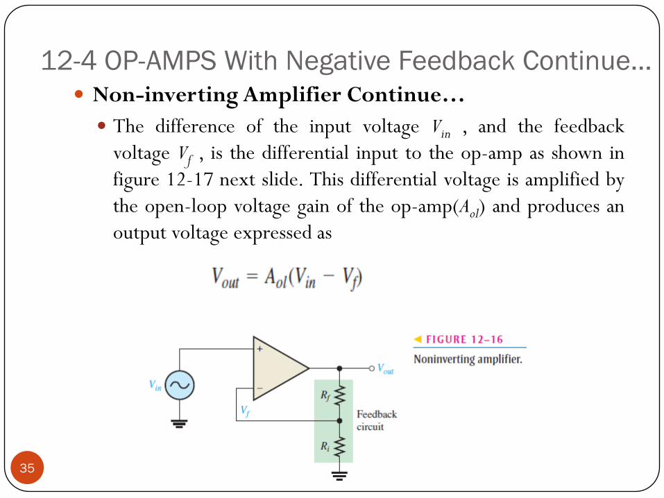
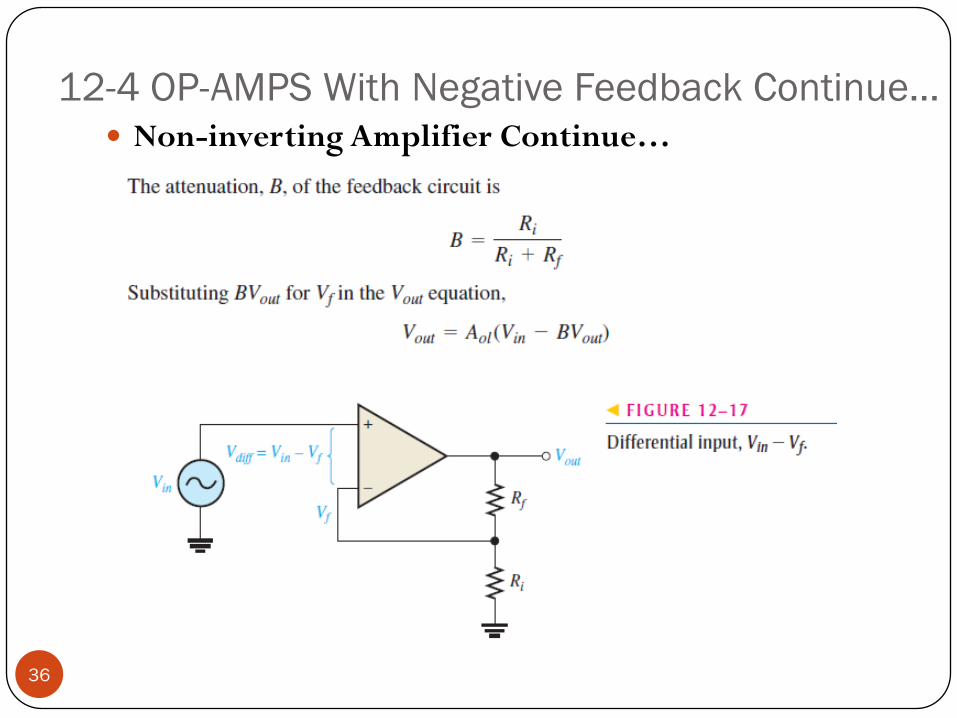
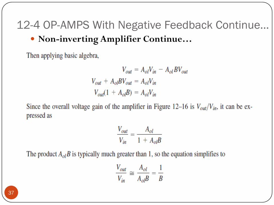
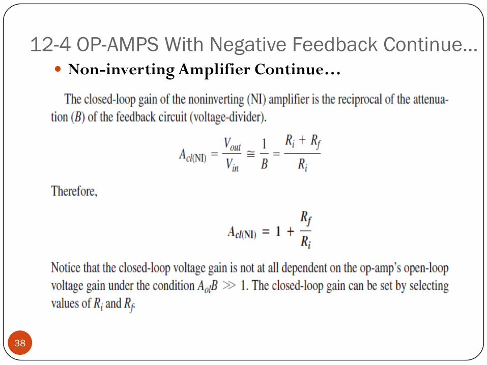
12-4 OP-AMPS With Negative Feedback Continue… Non-inverting Amplifier Continue…
The difference of the input voltage Vin , and the feedback
voltage Vf , is the differential input to the op-amp as shown in
figure 12-17 next slide. This differential voltage is amplified by
the open-loop voltage gain of the op-amp(Aol) and produces an
output voltage expressed as
35
12-4 OP-AMPS With Negative Feedback Continue… Non-inverting Amplifier Continue…
36
12-4 OP-AMPS With Negative Feedback Continue… Non-inverting Amplifier Continue…
37
12-4 OP-AMPS With Negative Feedback Continue… Non-inverting Amplifier Continue…
38
39
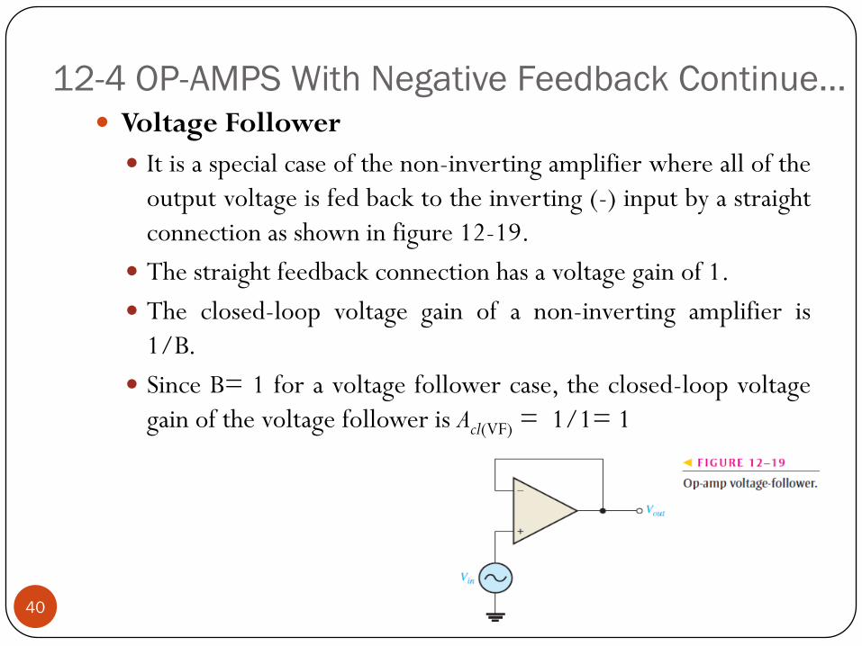
12-4 OP-AMPS With Negative Feedback Continue… Voltage Follower
It is a special case of the non-inverting amplifier where all of the
output voltage is fed back to the inverting (-) input by a straight
connection as shown in figure 12-19.
The straight feedback connection has a voltage gain of 1.
The closed-loop voltage gain of a non-inverting amplifier is
1/B.
Since B= 1 for a voltage follower case, the closed-loop voltage
gain of the voltage follower is Acl(VF) = 1/1= 1
40
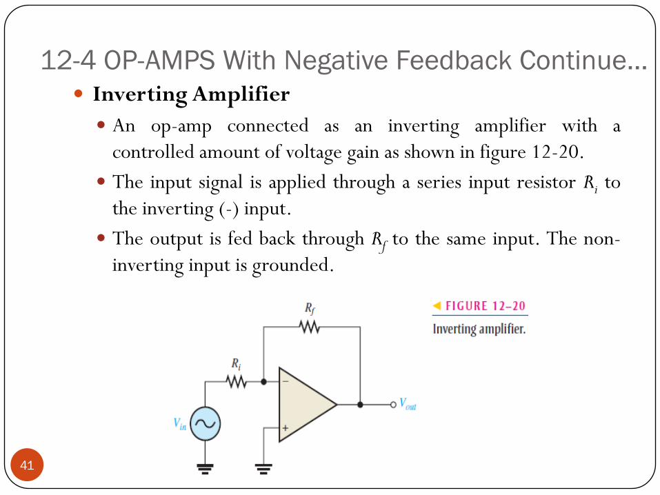
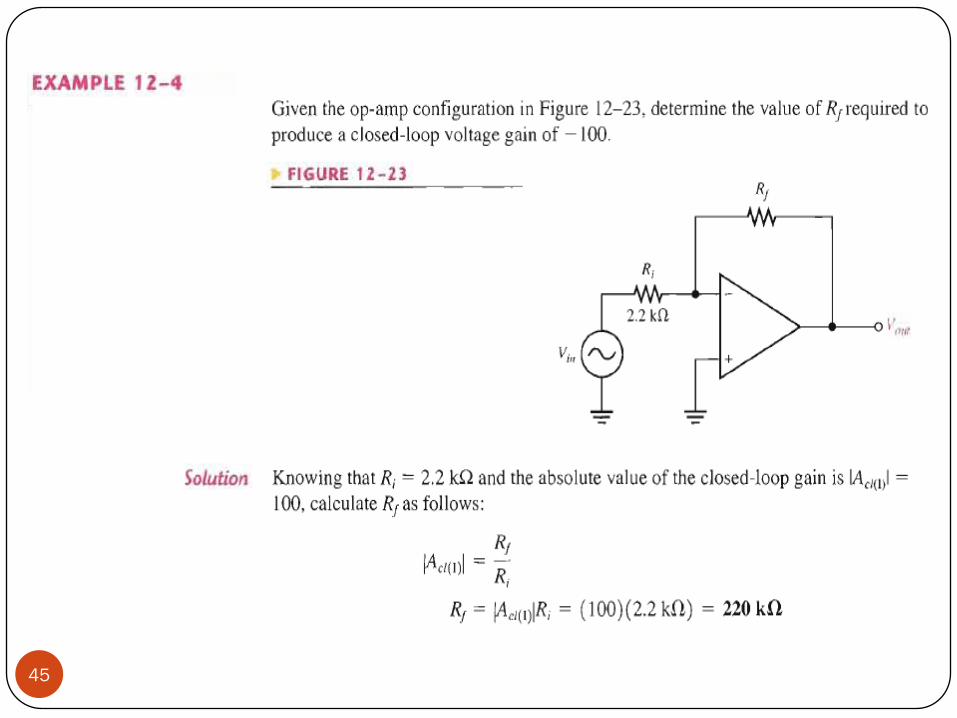
12-4 OP-AMPS With Negative Feedback Continue… Inverting Amplifier
An op-amp connected as an inverting amplifier with a
controlled amount of voltage gain as shown in figure 12-20.
The input signal is applied through a series input resistor Ri to
the inverting (-) input.
The output is fed back through Rf to the same input. The non-
inverting input is grounded.
41
12-4 OP-AMPS With Negative Feedback Continue… Inverting Amplifier Continue…
At this point, the ideal op-amp parameters mentioned earlier
are useful in simplifying the analysis of this circuit.
Particularly the concept of infinite input impedance is of great
value.
An infinite input impedance implies zero current at the
inverting input.
If there is zero current through the input impedance, then there
must be no voltage drop between the inverting and non-
inverting terminals.
This means that the voltage at the inverting (-) input is zero.
This zero voltage at the inverting input terminal is referred to as
virtual ground. This condition is illustrated in figure 12-21(a)
next slide.42
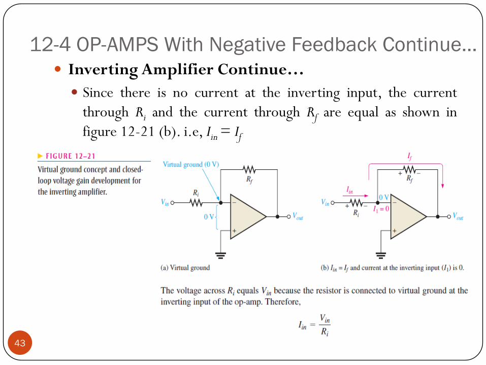
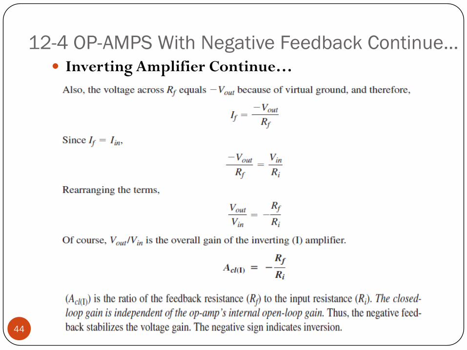
12-4 OP-AMPS With Negative Feedback Continue… Inverting Amplifier Continue…
Since there is no current at the inverting input, the current
through Ri and the current through Rf are equal as shown in
figure 12-21 (b). i.e, Iin= If
43
12-4 OP-AMPS With Negative Feedback Continue… Inverting Amplifier Continue…
44
45