Embed Size (px)
Citation preview

Made by
Chetan Kataria
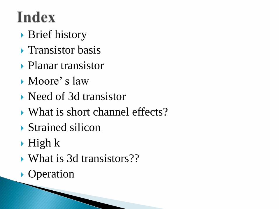
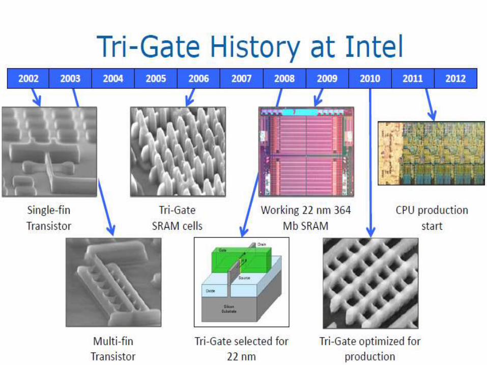
Brief history
Transistor basis
Planar transistor
Moore’ s law
Need of 3d transistor
What is short channel effects?
Strained silicon
High k
What is 3d transistors??
Operation
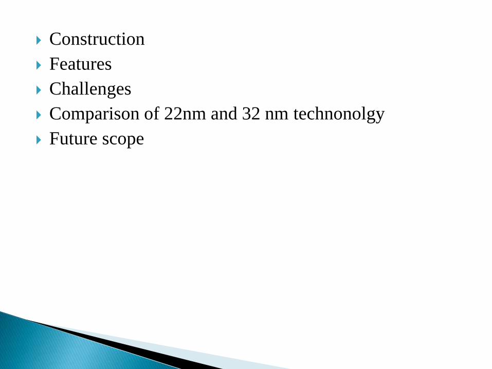
Construction
Features
Challenges
Comparison of 22nm and 32 nm technonolgy
Future scope
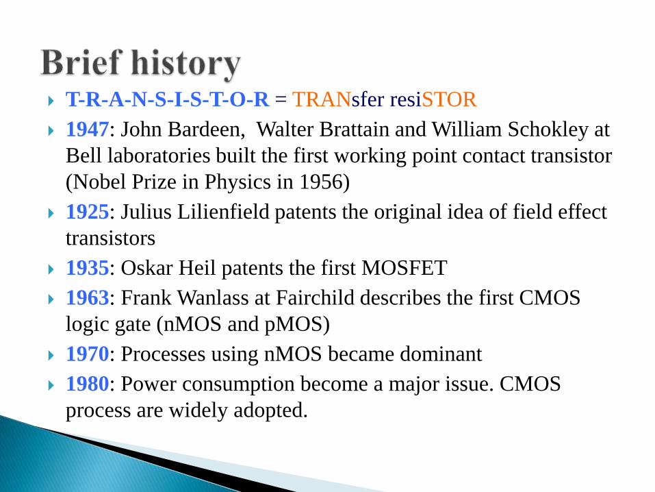
T-R-A-N-S-I-S-T-O-R = TRANsfer resiSTOR
1947: John Bardeen, Walter Brattain and William Schokley at
Bell laboratories built the first working point contact transistor
(Nobel Prize in Physics in 1956)
1925: Julius Lilienfield patents the original idea of field effect
transistors
1935: Oskar Heil patents the first MOSFET
1963: Frank Wanlass at Fairchild describes the first CMOS
logic gate (nMOS and pMOS)
1970: Processes using nMOS became dominant
1980: Power consumption become a major issue. CMOS
process are widely adopted.
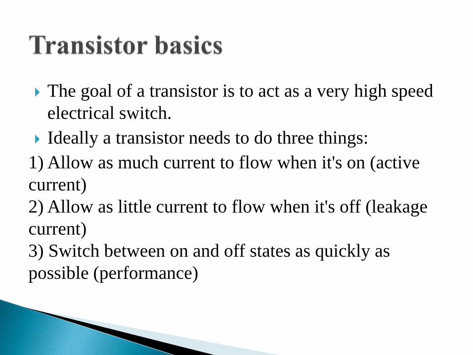
The goal of a transistor is to act as a very high speed
electrical switch.
Ideally a transistor needs to do three things:
1) Allow as much current to flow when it's on (active
current)
2) Allow as little current to flow when it's off (leakage
current)
3) Switch between on and off states as quickly as
possible (performance)

3 d view 2 d view

A transistor constructed by an etching and diffusion
technique in which the junction is never exposed
during processing, characterized by very low leakage
current and relatively high gain.
Working
1. The gate, oxide and bulk silicon act as a parallel
plate capacitor with the oxide layer.
2. If the gate is negatively biased with respect to the
source and substrate, the majority carriers
(electrons) in the bulk n-type silicon are forced away
from the Si/SiO2 interface and a depletion region is
formed.
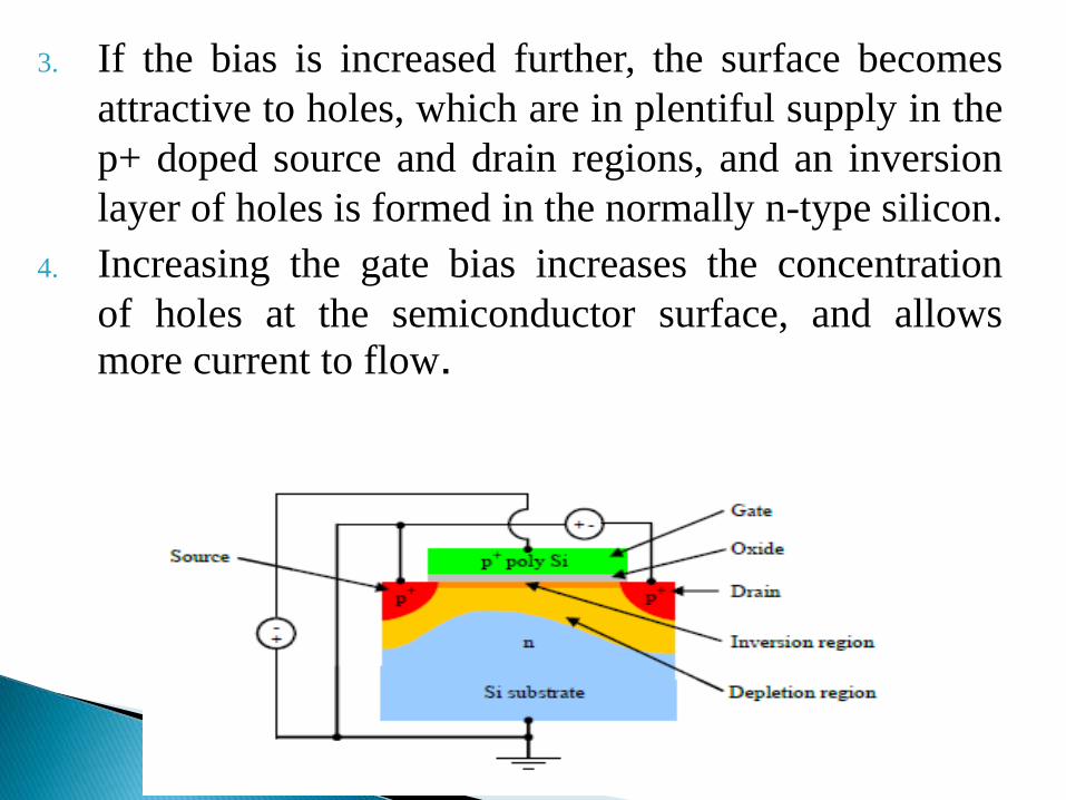
3. If the bias is increased further, the surface becomes
attractive to holes, which are in plentiful supply in the
p+ doped source and drain regions, and an inversion
layer of holes is formed in the normally n-type silicon.
4. Increasing the gate bias increases the concentration
of holes at the semiconductor surface, and allowsmore current to flow.

In 1963 Gordon Moore predicted that the number of
transistors on an integrated circuit doubles
approximately every two years which is achieved by
scaling down the transistor size.
According to Intel, Tri-Gate was implemented
because it would not have been possible to
continue Moore's law at 22nm and below without a
major transistor redesign. With Tri-Gate transistors,
Intel claims to have extended Moore's law at least
another two years.

Smaller is faster
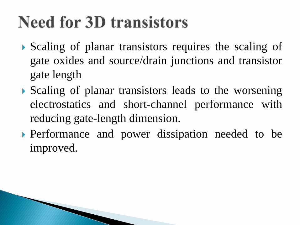
Scaling of planar transistors requires the scaling of
gate oxides and source/drain junctions and transistor
gate length
Scaling of planar transistors leads to the worsening
electrostatics and short-channel performance with
reducing gate-length dimension.
Performance and power dissipation needed to be
improved.
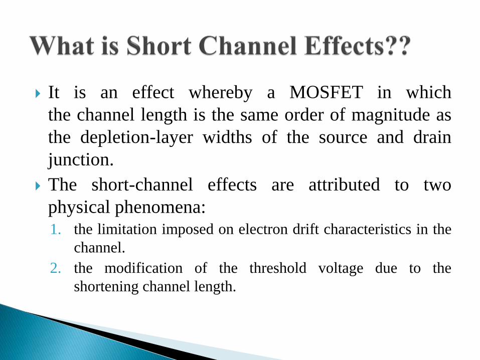
It is an effect whereby a MOSFET in which
the channel length is the same order of magnitude as
the depletion-layer widths of the source and drain
junction.
The short-channel effects are attributed to two
physical phenomena:1. the limitation imposed on electron drift characteristics in the
channel.
2. the modification of the threshold voltage due to the
shortening channel length.
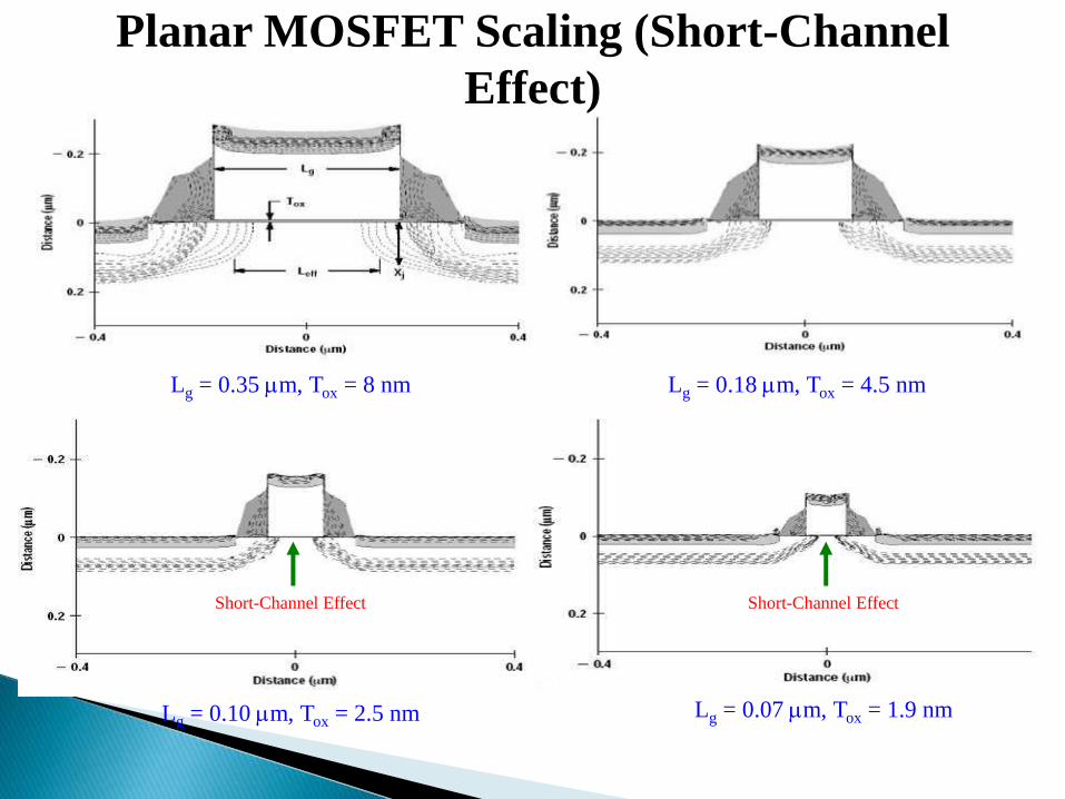
Planar MOSFET Scaling (Short-Channel
Effect)
Lg = 0.35 m, Tox = 8 nm Lg = 0.18 m, Tox = 4.5 nm
Lg = 0.10 m, Tox = 2.5 nm Lg = 0.07 m, Tox = 1.9 nm
Short-Channel EffectShort-Channel Effect

Strain techniques, such as incorporating SiGe, have
boosted the performance in of CMOS silicon
transistors.
Global strain-Stress is introduced across the entire
substrate. This is done by growing a SiGe ‘buffer
layer’ on top of the silicon substrate. The main
advantage of this approach is that it creates biaxial
stress and thus can be used for both pMOS and
nMOS devices.
Local strain-it is based on stress liners refers to a
technique where stress is engineered into the
transistor channel by means of dielectric layers which
are deposited around the gate.
Drawback of technology-
1. Limited 45 nm technology
2. For dense 45 nm transistor layouts, a larger volume
of SiGe is present resulting in higher stress values
and faster saturation levels .

Introducing higher dielectric constant (k > 10) insulators
is therefore indispensable for the 70 nm technology
node and beyond, despite the fact that most of the high-
k materials have much poorer properties than the
conventional silicon oxide
Various technologies are used to deposit high k on
substrate such as
(i) chemical vapor deposition (CVD),
(ii) metal organic CVD (MOCVD),
(iii) atomic layer deposition(ALD),
(iv) Physical vapor deposition,
(v) ion beam assisted deposition,

Drawbacks
The major problem in high-k materials is that they are
yet to meet the electrical characteristics that SiO2 can
offer.

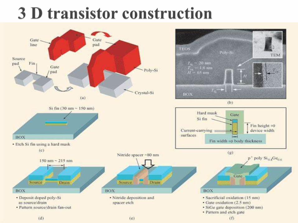
The Tri-Gate technology gets its name from the fact
that transistors using it have conducting channels
that are formed on all three sides—two on each
side, one across the top—of a tall and narrow
silicon fin that rises vertically from the silicon
substrate.
The Gate is the terminal that drives the transistor on
and off, and acts like a capacitance where charge is
stored making the channel conductive.

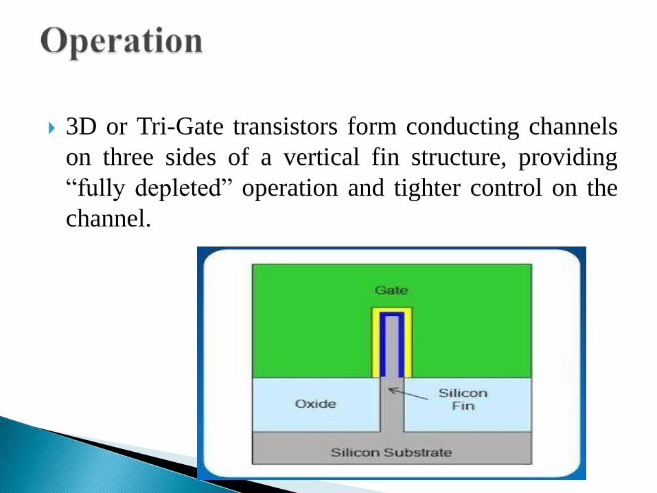
3D or Tri-Gate transistors form conducting channels
on three sides of a vertical fin structure, providing
“fully depleted” operation and tighter control on the
channel.
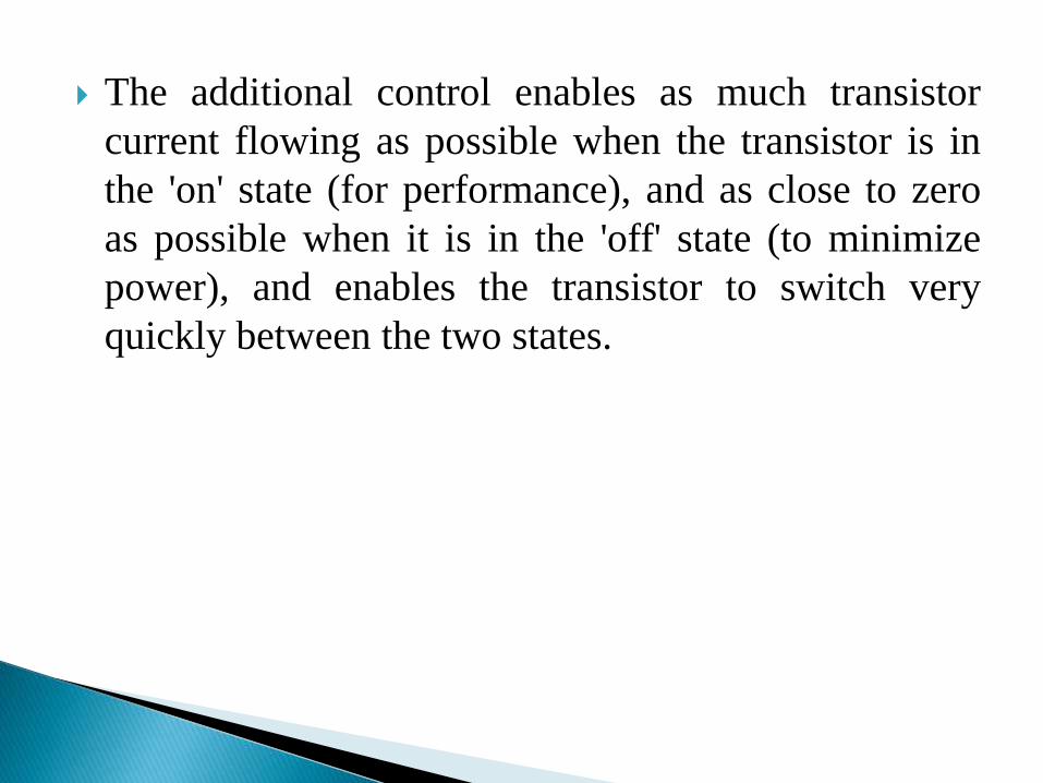
The additional control enables as much transistor
current flowing as possible when the transistor is in
the 'on' state (for performance), and as close to zero
as possible when it is in the 'off' state (to minimize
power), and enables the transistor to switch very
quickly between the two states.
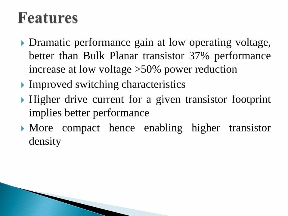
Dramatic performance gain at low operating voltage,
better than Bulk Planar transistor 37% performance
increase at low voltage >50% power reduction
Improved switching characteristics
Higher drive current for a given transistor footprint
implies better performance
More compact hence enabling higher transistor
density

The primary challenges to integrating non planar tri gate
devices into conventional semiconductor manufacturing
processes include:
Fabrication of a thin silicon "fin" tens of nanometers
wide
Fabrication of matched gates on multiple sides of the
fin
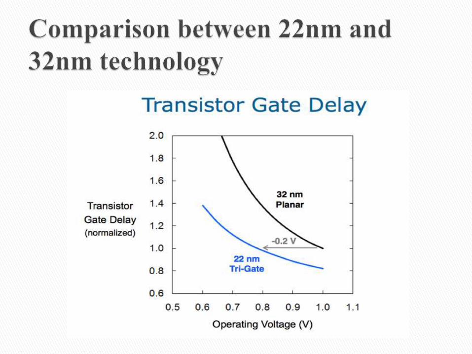

At the same switching speed, Intel's 22nm 3D Tri-
Gate transistors can run at 75 - 80% of the
operating voltage of Intel's 32nm transistors. This
results in lower active power at the same
frequency.
It will only add 2 to 3 percent to the cost of a
finished wafer.

The 3-D Tri-Gate transistor is a variant of the FinFETdeveloped at UC-Berkeley, and is being used in Intel’s 22nm-generation microprocessors.

Ivy Bridge-based Intel®Core™ family processorswill be the first high-volume chips to use 3-DTri-Gate transistors.
This silicon technologybreakthrough will also aidin the delivery of morehighly integrated Intel®Atom™ processor-basedproducts…
28http://newsroom.intel.com/community/intel_newsroom/blog/2011/05/04/intel-reinvents-transistors-using-new-3-d-structure

The new chip technology called tri gate transistors
replaces the 2 dimensional streams of transistors with
3d structure.
The technology will allow to manufacture to create
transistors that are faster, smaller and more powerful
efficient which will be used in next generation laptop
and other gadgets.
Tri gate transistors are important innovation needed to
continue Moore’s law

[1] Isabelle Ferain, Cynthia A. Colinge & Jean-PierreColinge, “Multigate transistors as the future of classicalmetal-oxide semiconductor field effects transistors”.
[2] Aniket A. Breed/ Dr. Marc Cahay, “Design andEvolution of modern SOI fully-depleted MOSFETs”.
[3] Jack Kavalieros, Brian Doyle, “ Tri-Gate TransistorArchitecture with High-k Gate Dielectrics, Metal Gates”.
[4] Viranjay M. Srivastava, Setu P. Singh, ”Analysis andDesign of Tri-Gate MOSFET with High Dielectrics Gate”.
[5] http://en.wikipedia.org/wiki/Multigate_device
[6]http://www.intel.com/content/www/us/en/energy/intel22nm-3-d-tri-gate-transistor-technology.html