Crystalline silicon cantilevers for piezoresistive detection
of biomolecular forces
G. Villanuevaa,b, J.A. Plazaa, J. Montserrata, F. Perez-Muranoa and J. Bausellsa
a Centro Nacional de Microelectrónica (IMB-CSIC), 08193 Bellaterra, Spain
phone: +34–93 594 7700. e-mail: [email protected]
b Microsystems Laboratory, EPFL, Lausanne, CH-1015 Switzerland.
phone: +41–21–6937818 e-mail: [email protected]
Abstract
In order to obtain a sensor with force resolution better than 100 pN for biomolecular
detection, U-shaped piezoresistive cantilevers made of crystalline silicon have been
fabricated. The resistors have been defined by ionic implantation of As+, yielding a shallow
and thin resistor and they have been patterned parallel to the (100) crystallographic direction,
attaining a maximum for the piezoresistive factor. The sensitivity of the devices is
characterized together as the force resolution, being both of them 60 V/pN and 65 pN
respectively, for a cantilever with a length of 250 m, a width of 8 m and a thickness of 340
nm.
Keywords: Piezoresistive cantilever, crystalline silicon, force detection
* Manuscript
1. Introduction
Silicon microcantilevers were originally developed for atomic force microscopy (AFM), but
in the last decade they have been increasingly used for biochemical sensing [1]. In this case,
cantilevers are typically used to detect the binding of biomolecules to their functionalised
surface, by measuring either the deflection in static mode [2] or the change resonant
frequency mass in the dynamic mode [3]. An additional possibility, with potentially a high
sensitivity, is the detection of the intermolecular forces between a functionalised AFM tip and
a surface [4].
The motivation of the present work is to achieve the detection of proteins by a static
measurement of the molecular binding between a cantilever and a substrate in a portable
instrument. Such detection implies the measurement of forces below 100 pN, which requires
submicron thick cantilevers [5]. As the optical detection cannot be used in a portable, robust
device, the deflection was chosen to be measured by means of a piezoresistor integrated in
the cantilever. We have presented elsewhere the fabrication of polycrystalline silicon beams
without [5] and with [6] integrated signal processing circuitry. The reason to use
polycrystalline silicon was the compatibility with the on-chip circuit integration. In order to
improve the performance of the mechanical part of the sensor, we now report the fabrication
of crystalline silicon microcantilevers, with a much higher piezoresistance coefficient than
that of polysilicon [7].
Crystalline silicon piezoresistive microcantilevers have been developed using various
approaches. Tortonese et al. [8] fabricated AFM cantilevers by using silicon-on-insulator
(SOI) wafers and standard boron implantation to define the piezoresistors. The cantilevers
had a thickness of 2 µm (length L=175 µm) and a spring constant k= 4 N/m. Fabricating
piezoresistors in crystalline silicon with a total cantilever thickness of 1 µm or less is
challenging. Ried et al. [9] made 0.34 µm-thick AFM cantilevers by using a 10 keV low
energy B implantation, and using a low temperature oxide for passivation. Harley and Kenny
[10] fabricated very thin (90 nm) cantilevers (L=350 µm) with very low spring constants
(3·10-5 N/m), by using an epitaxial deposition process to grow a boron-doped crystalline
silicon layer for the piezoresistors. They obtained a force sensitivity of 40 nV/pN provided a
supply voltage of 1 V. In all these cases p-type piezoresistors were used, and the resistors and
the cantilevers have the standard (110) orientation (parallel to the main wafer flat) on a
<100> silicon wafer. We have fabricated our cantilevers with n-type doping and with a
different (100) orientation. In section 2 we discuss the cantilever design considerations and
fabrication technology together with the advantages of using n-type piezoresistors, in terms
of pn junction depth and piezoresistive coefficient. In section 3 the characterization results
are presented.
2. Cantilever design and fabrication
In order to achieve high force sensitivity it is necessary to have a cantilever as thin as
possible and with the resistance as far as possible from the neutral axis of the structure. As
discussed above, all Si piezoresistive microcantilevers have been fabricated to date using p-
type B-doped resistors, despite the maximum value of the longitudinal piezoresistive
coefficient (l) for n-type Si is higher (45% larger, along (100) direction) than that of p-type
Si (along (110) direction) [11]. Also, it is difficult to obtain shallow (< 0.5 µm) B-doped pn
junctions by ion implantation. The reason why p-type doping is used is related to the
dependence of l of Si on the crystallographic axes. On a standard <100> silicon wafer, the
piezoresistors and the cantilevers are oriented in the (110) direction. This is the standard
orientation of the primary flat on silicon wafers, and thus the photolithography mask designs
and silicon chips are normally parallel to it. In addition, the <111> planes defined by wet
anisotropic etching are also aligned to the (110) directions on the wafer surface and, in the
(110) direction, l of p-type silicon has a maximum whereas that of n-type silicon has a
minimum [11]. For this reason it is usually advantageous to use p-type doping. To obtain a
shallow pn junction, however, it is beneficial to implant a heavy ion, such as As, due to the
reduced ion penetration range and a diffusion coefficient in Si smaller than boron [12]. This
requires however a change in the orientation of the cantilevers and the piezoresistors. We
have therefore oriented our cantilevers in the (100) direction, and we have used As-implanted
n-type piezoresistors on a p-type substrate. In addition, the Young modulus of Si in (100)
direction is minimum [13], which results in softer cantilevers. This novel definition of the
cantilevers (forming 45º with the flat of a standard <100> wafer) is allowed by the use of a
deep reactive ion etching (DRIE) process (which is unrelated to the Si crystallographic
planes) to perform the bulk machining.
All the cantilevers have been designed with a U-shape to minimize the width of the
piezoresistor areas, as in most of the above referenced devices. In addition, they are designed
as part of resistive Wheatstone bridges or semi-bridges.
The fabrication starts with a SOI wafer with a 340 nm thick top p-type (0.1-10 Ω·cm) silicon
layer (Fig.1.a). The resistors are implanted at 50 keV using As ions and the cantilevers are
defined (Fig.1.b). The resistors and cantilevers are patterned along a (100) axis of the
crystalline silicon. A thin oxide (35 nm) is grown at 900 C in order to isolate the resistor and
at the same time activate the impurities. The contacts are opened and the metal (1 m thick
aluminum) for the paths is sputtered and then patterned by a dry etching (Fig. 1.c). A PECVD
silicon nitride layer (100 nm thick) is patterned on the front side in order to passivate the
metal paths and also the piezoresistor (Fig. 1.d). On the backside, an Al layer is deposited and
structured in order to define a hard mask for the back-side DRIE etching of the whole silicon
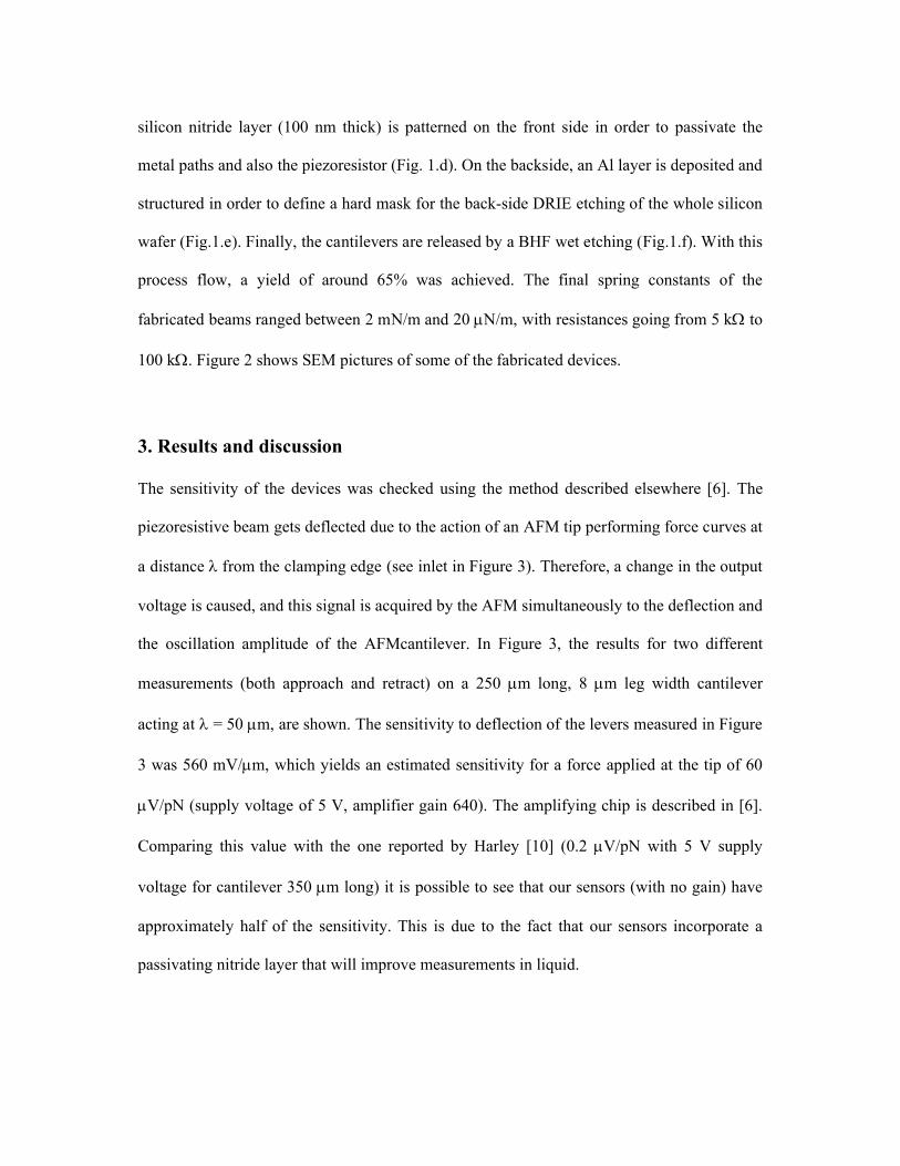
wafer (Fig.1.e). Finally, the cantilevers are released by a BHF wet etching (Fig.1.f). With this
process flow, a yield of around 65% was achieved. The final spring constants of the
fabricated beams ranged between 2 mN/m and 20 N/m, with resistances going from 5 k to
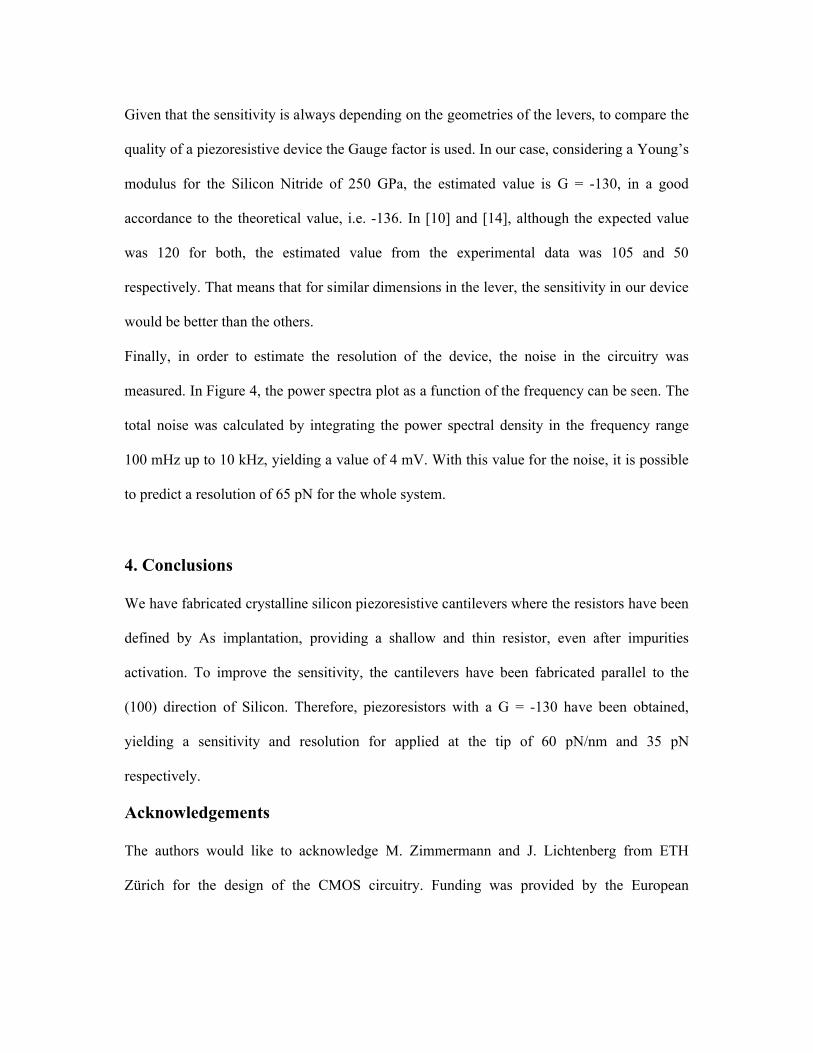
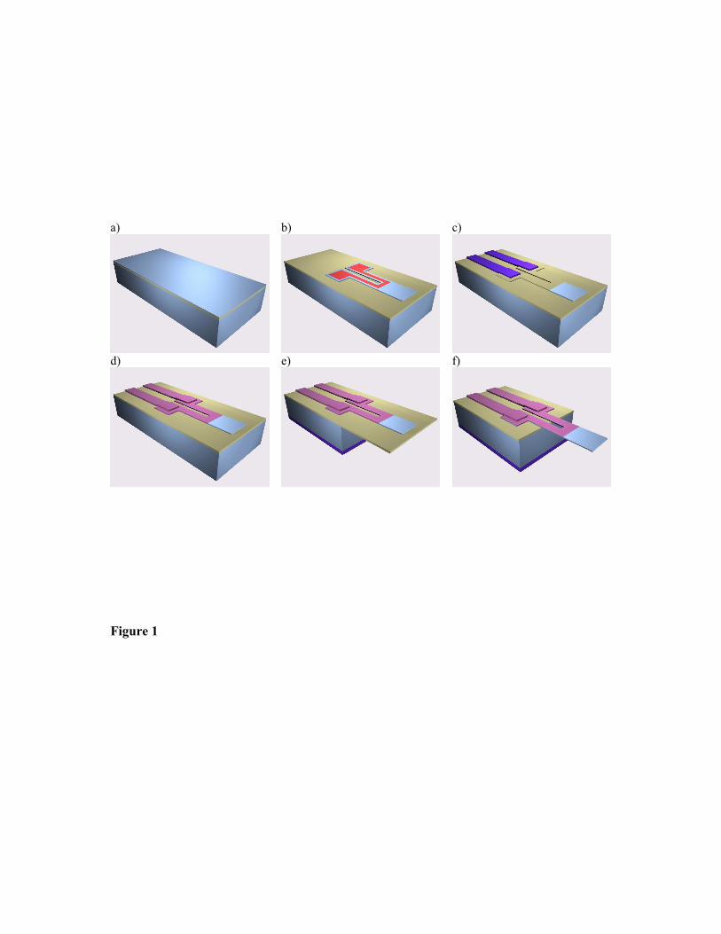
100 k. Figure 2 shows SEM pictures of some of the fabricated devices.
3. Results and discussion
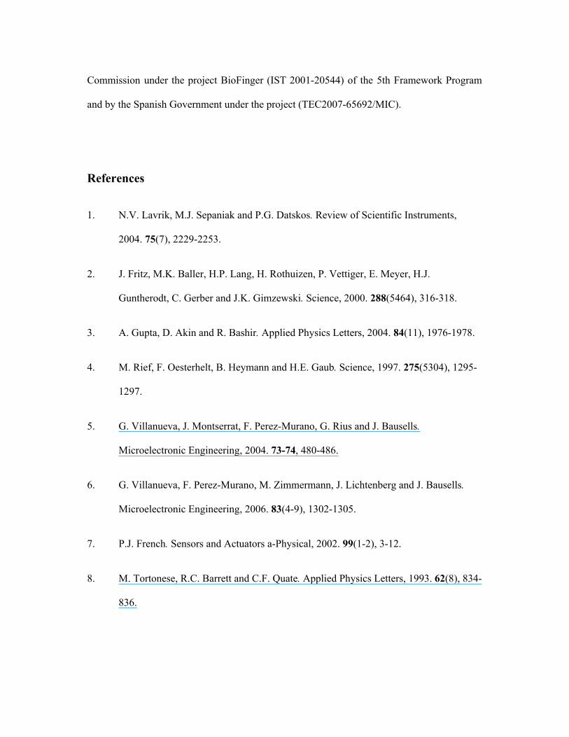
The sensitivity of the devices was checked using the method described elsewhere [6]. The
piezoresistive beam gets deflected due to the action of an AFM tip performing force curves at
a distance from the clamping edge (see inlet in Figure 3). Therefore, a change in the output
voltage is caused, and this signal is acquired by the AFM simultaneously to the deflection and
the oscillation amplitude of the AFMcantilever. In Figure 3, the results for two different
measurements (both approach and retract) on a 250 m long, 8 m leg width cantilever
acting at = 50 m, are shown. The sensitivity to deflection of the levers measured in Figure
3 was 560 mV/m, which yields an estimated sensitivity for a force applied at the tip of 60
V/pN (supply voltage of 5 V, amplifier gain 640). The amplifying chip is described in [6].
Comparing this value with the one reported by Harley [10] (0.2 V/pN with 5 V supply
voltage for cantilever 350 m long) it is possible to see that our sensors (with no gain) have
approximately half of the sensitivity. This is due to the fact that our sensors incorporate a
passivating nitride layer that will improve measurements in liquid.
Given that the sensitivity is always depending on the geometries of the levers, to compare the
quality of a piezoresistive device the Gauge factor is used. In our case, considering a Young’s
modulus for the Silicon Nitride of 250 GPa, the estimated value is G = -130, in a good
accordance to the theoretical value, i.e. -136. In [10] and [14], although the expected value
was 120 for both, the estimated value from the experimental data was 105 and 50
respectively. That means that for similar dimensions in the lever, the sensitivity in our device
would be better than the others.
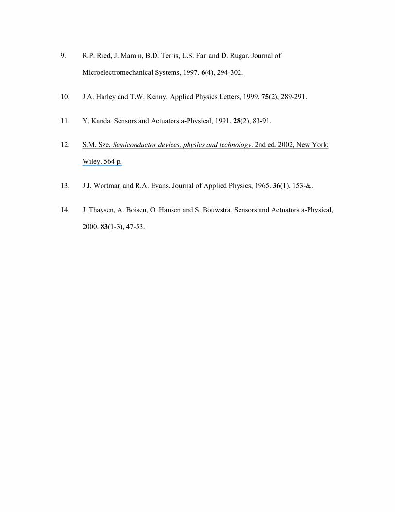
Finally, in order to estimate the resolution of the device, the noise in the circuitry was
measured. In Figure 4, the power spectra plot as a function of the frequency can be seen. The
total noise was calculated by integrating the power spectral density in the frequency range
100 mHz up to 10 kHz, yielding a value of 4 mV. With this value for the noise, it is possible
to predict a resolution of 65 pN for the whole system.
4. Conclusions
We have fabricated crystalline silicon piezoresistive cantilevers where the resistors have been
defined by As implantation, providing a shallow and thin resistor, even after impurities
activation. To improve the sensitivity, the cantilevers have been fabricated parallel to the
(100) direction of Silicon. Therefore, piezoresistors with a G = -130 have been obtained,
yielding a sensitivity and resolution for applied at the tip of 60 pN/nm and 35 pN
respectively.
Acknowledgements
The authors would like to acknowledge M. Zimmermann and J. Lichtenberg from ETH
Zürich for the design of the CMOS circuitry. Funding was provided by the European
Commission under the project BioFinger (IST 2001-20544) of the 5th Framework Program
and by the Spanish Government under the project (TEC2007-65692/MIC).
References
1. N.V. Lavrik, M.J. Sepaniak and P.G. Datskos. Review of Scientific Instruments,
2004. 75(7), 2229-2253.
2. J. Fritz, M.K. Baller, H.P. Lang, H. Rothuizen, P. Vettiger, E. Meyer, H.J.
Guntherodt, C. Gerber and J.K. Gimzewski. Science, 2000. 288(5464), 316-318.
3. A. Gupta, D. Akin and R. Bashir. Applied Physics Letters, 2004. 84(11), 1976-1978.
4. M. Rief, F. Oesterhelt, B. Heymann and H.E. Gaub. Science, 1997. 275(5304), 1295-
1297.
5. G. Villanueva, J. Montserrat, F. Perez-Murano, G. Rius and J. Bausells.
Microelectronic Engineering, 2004. 73-74, 480-486.
6. G. Villanueva, F. Perez-Murano, M. Zimmermann, J. Lichtenberg and J. Bausells.
Microelectronic Engineering, 2006. 83(4-9), 1302-1305.
7. P.J. French. Sensors and Actuators a-Physical, 2002. 99(1-2), 3-12.
8. M. Tortonese, R.C. Barrett and C.F. Quate. Applied Physics Letters, 1993. 62(8), 834-
836.
9. R.P. Ried, J. Mamin, B.D. Terris, L.S. Fan and D. Rugar. Journal of
Microelectromechanical Systems, 1997. 6(4), 294-302.
10. J.A. Harley and T.W. Kenny. Applied Physics Letters, 1999. 75(2), 289-291.
11. Y. Kanda. Sensors and Actuators a-Physical, 1991. 28(2), 83-91.
12. S.M. Sze, Semiconductor devices, physics and technology. 2nd ed. 2002, New York:
Wiley. 564 p.
13. J.J. Wortman and R.A. Evans. Journal of Applied Physics, 1965. 36(1), 153-&.
14. J. Thaysen, A. Boisen, O. Hansen and S. Bouwstra. Sensors and Actuators a-Physical,
2000. 83(1-3), 47-53.
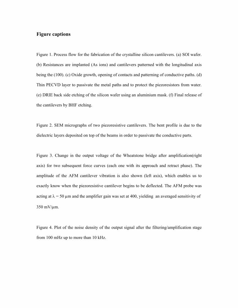
Figure captions
Figure 1. Process flow for the fabrication of the crystalline silicon cantilevers. (a) SOI wafer.
(b) Resistances are implanted (As ions) and cantilevers patterned with the longitudinal axis
being the (100). (c) Oxide growth, opening of contacts and patterning of conductive paths. (d)
Thin PECVD layer to passivate the metal paths and to protect the piezoresistors from water.
(e) DRIE back side etching of the silicon wafer using an aluminium mask. (f) Final release of
the cantilevers by BHF etching.
Figure 2. SEM micrographs of two piezoresistive cantilevers. The bent profile is due to the
dielectric layers deposited on top of the beams in order to passivate the conductive parts.
Figure 3. Change in the output voltage of the Wheatstone bridge after amplification(right
axis) for two subsequent force curves (each one with its approach and retract phase). The
amplitude of the AFM cantilever vibration is also shown (left axis), which enables us to
exactly know when the piezoresistive cantilever begins to be deflected. The AFM probe was
acting at = 50 m and the amplifier gain was set at 400, yielding an averaged sensitivity of
350 mV/m.
Figure 4. Plot of the noise density of the output signal after the filtering/amplification stage
from 100 mHz up to more than 10 kHz.
a) b) c)
d) e) f)
Figure 1
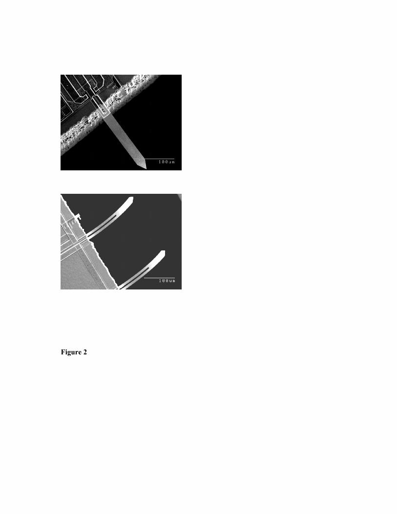
Figure 2
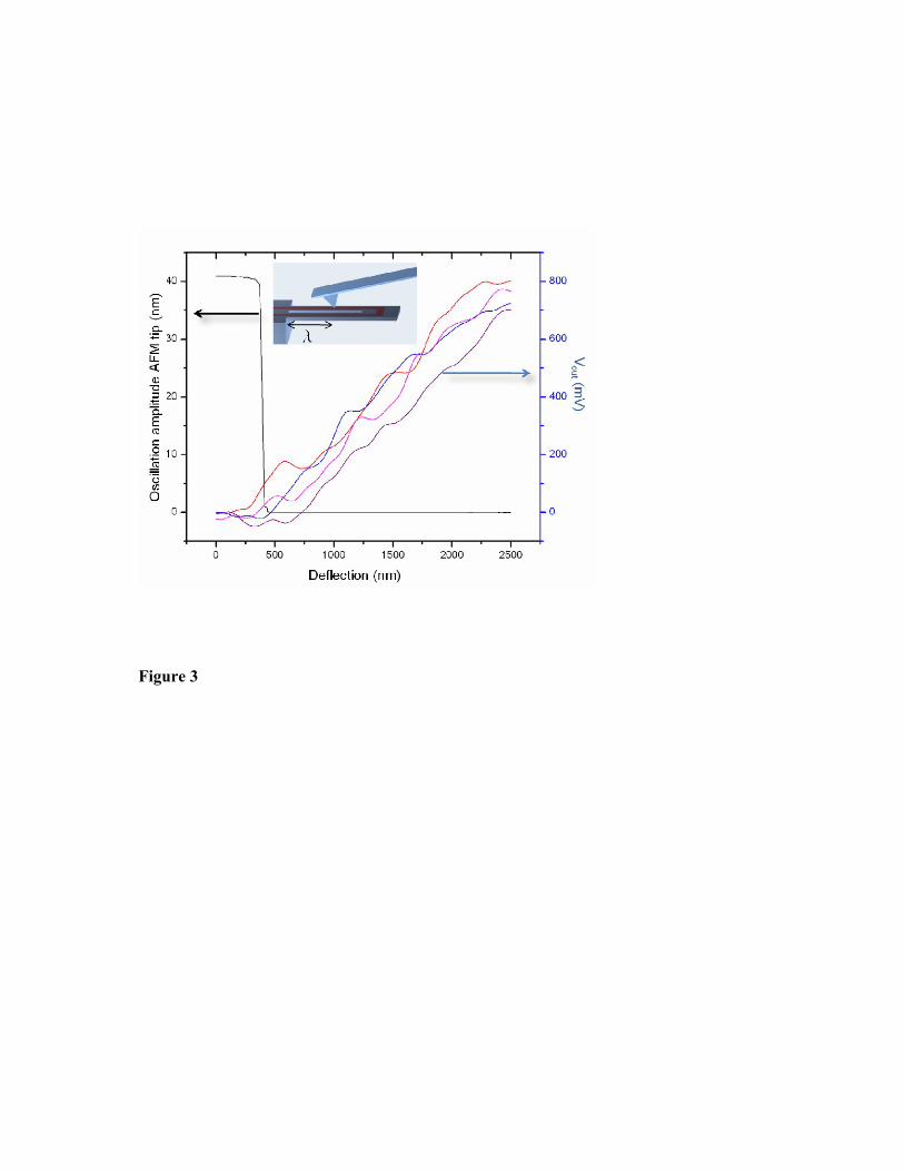
Figure 3
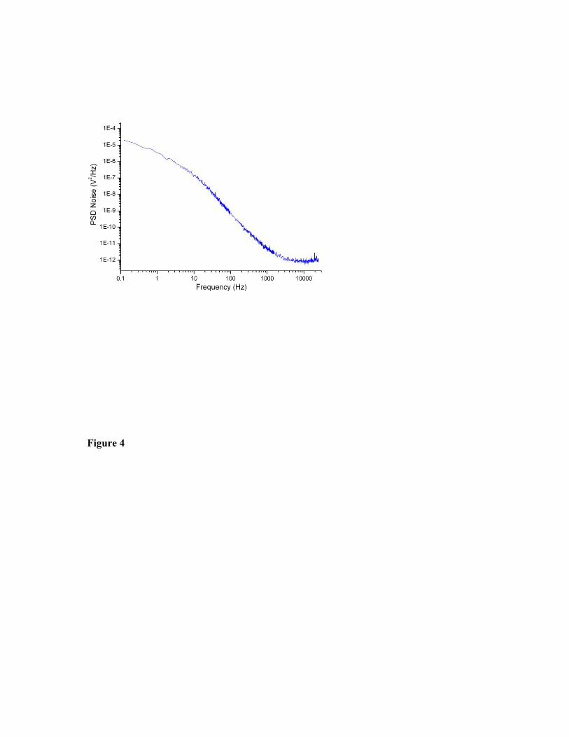
Figure 4
Recommended


