LM392-N
www.ti.com SNOSBT5D –APRIL 1998–REVISED MARCH 2013
lm392-N Low Power Operational Amplifier/Voltage ComparatorCheck for Samples: LM392-N
1FEATURES DESCRIPTIONThe lm392-N series consists of 2 independent
2• Wide Power Supply Voltage Rangebuilding block circuits. One is a high gain, internally
– Single Supply: 3V to 32V frequency compensated operational amplifier, and the– Dual Supply: ±1.5V to ±16V other is a precision voltage comparator. Both the
operational amplifier and the voltage comparator• Low Supply Current Drain—Essentiallyhave been specifically designed to operate from aIndependent of Supply Voltage: 600 μAsingle power supply over a wide range of voltages.
• Low Input Biasing Current: 50 nA Both circuits have input stages which will common-• Low Input Offset Voltage: 2 mV mode input down to ground when operating from a
single power supply. Operation from split power• Low Input Offset Current: 5 nAsupplies is also possible and the low power supply• Input Common-Mode Voltage Range Includes current is independent of the magnitude of the supply
Ground voltage.• Differential Input Voltage Range Equal to the
Application areas include transducer amplifier withPower Supply Voltagepulse shaper, DC gain block with level detector, VCO,
• ADDITIONAL OP AMP FEATURES as well as all conventional operational amplifier orvoltage comparator circuits. Both circuits can be– Internally Frequency Compensated foroperated directly from the standard 5 VDC powerUnity Gainsupply voltage used in digital systems, and the output– Large DC Voltage Gain: 100 dBof the comparator will interface directly with either
– Wide Bandwidth (Unity Gain): 1 MHz TTL or CMOS logic. In addition, the low power drainmakes the lm392-N extremely useful in the design of– Large Output Voltage Swing: 0V to V+ −portable equipment.1.5V
• ADDITIONAL COMPARATOR FEATURES– Low Output Saturation Voltage: 250 mV at 4
mA– Output Voltage Compatible with all Types
of Logic Systems
ADVANTAGES• Eliminates Need for Dual Power Supplies• An Internally Compensated Op Amp and a
Precision Comparator in the Same Package• Allows Sensing at or Near Ground• Power Drain Suitable for Battery Operation• Pin-Out is the Same as Both the LM358 Dual
Op Amp and the LM393 Dual Comparator
1
Please be aware that an important notice concerning availability, standard warranty, and use in critical applications ofTexas Instruments semiconductor products and disclaimers thereto appears at the end of this data sheet.
2All trademarks are the property of their respective owners.
PRODUCTION DATA information is current as of publication date. Copyright © 1998–2013, Texas Instruments IncorporatedProducts conform to specifications per the terms of the TexasInstruments standard warranty. Production processing does notnecessarily include testing of all parameters.
LM392-N
SNOSBT5D –APRIL 1998–REVISED MARCH 2013 www.ti.com
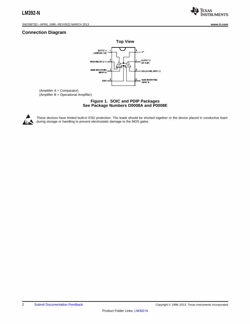
Connection Diagram
Top View
(Amplifier A = Comparator)(Amplifier B = Operational Amplifier)
Figure 1. SOIC and PDIP PackagesSee Package Numbers D0008A and P0008E
These devices have limited built-in ESD protection. The leads should be shorted together or the device placed in conductive foamduring storage or handling to prevent electrostatic damage to the MOS gates.
2 Submit Documentation Feedback Copyright © 1998–2013, Texas Instruments Incorporated
Product Folder Links: LM392-N
LM392-N
www.ti.com SNOSBT5D –APRIL 1998–REVISED MARCH 2013
Absolute Maximum Ratings (1) (2)
lm392-N
Supply Voltage, V+ 32V or ±16V
Differential Input Voltage 32V
Input Voltage −0.3V to +32V
Power Dissipation (3)
Molded DIP (LM392N) 820 mW
Small Outline Package (LM392M) 530 mW
Output Short-Circuit to Ground (4) Continuous
Input Current (VIN < −0.3 VDC) (5) 50 mA
Operating Temperature Range 0°C to +70°C
Storage Temperature Range −65°C to +150°C
Lead Temperature (Soldering, 10 seconds) 260°C
ESD rating to be determined.
Soldering Information
Dual-in-Line Package
Soldering (10 seconds) 260°C
Small Outline Package
Vapor Phase (60 seconds) 215°C
Infrared (15 seconds) 220°C
(1) “Absolute Maximum Ratings” indicate limits beyond which damage to the device may occur. Operating Ratings indicate conditions forwhich the device is functional, but do not ensure specific performance limits.
(2) If Military/Aerospace specified devices are required, please contact the Texas Instruments Sales Office/Distributors for availability andspecifications.
(3) For operating at temperatures above 25°C, the lm392-N must be derated based on a 125°C maximum junction temperature and athermal resistance of 122°C/W which applies for the device soldered in a printed circuit board, operating in still air ambient. Thedissipation is the total of both amplifiers—use external resistors, where possible, to allow the amplifier to saturate or to reduce the powerwhich is dissipated in the integrated circuit.
(4) Short circuits from the output to V+ can cause excessive heating and eventual destruction. When considering short circuits to ground,the maximum output current is approximately 40 mA for the op amp and 30 mA for the comparator independent of the magnitude of V+.At values of supply voltage in excess of 15V, continuous short circuits can exceed the power dissipation ratings and cause eventualdestruction.
(5) This input current will only exist when the voltage at any of the input leads is driven negative. It is due to the collector-base junction ofthe input PNP transistors becoming forward biased and thereby acting as input diode clamps. In addition to this diode action, there isalso lateral NPN parasitic transistor action on the IC chip. This transistor action can cause the output voltages of the amplifiers to go tothe V+ voltage level (or to ground for a large overdrive) for the time duration that an input is driven negative. This is not destructive andnormal output states will re-establish when the input voltage, which was negative, again returns to a value greater than −0.3V (at 25°C).
Electrical Characteristics(V+ = 5 VDC; specifications apply to both amplifiers unless otherwise stated) (1)
lm392-NParameter Conditions Units
Min Typ Max
Input Offset Voltage TA = 25°C, (2) ±2 ±5 mV
Input Bias Current IN(+) or IN(−), TA =25°C, (3) , VCM = 0V 50 250 nA
Input Offset Current IN(+) − IN(−), TA = 25°C ±5 ±50 nA
Input Common-Mode Voltage Range V+ = 30 VDC, TA = 25°C, (4) 0 V+−1.5 V
Supply Current RL = ∞ , V+= 30 V 1 2 mA
Supply Current RL = ∞ , V+= 5 V 0.5 1 mA
(1) These specifications apply for V+ = 5V, unless otherwise stated. For the lm392-N, temperature specifications are limited to 0°C ≤ TA ≤+70°C.
(2) At output switch point, VO ≃ 1.4V, RS = 0Ω with V+ from 5V to 30V; and over the full input common-mode range (0V to V+ − 1.5V).(3) The direction of the input current is out of the IC due to the PNP input stage. This current is essentially constant, independent of the
state of the output so no loading change exists on the input lines.(4) The input common-mode voltage or either input signal voltage should not be allowed to go negative by more than 0.3V. The upper end
of the common-mode voltage range is V+ − 1.5V, but either or both inputs can go to 32V without damage.
Copyright © 1998–2013, Texas Instruments Incorporated Submit Documentation Feedback 3
Product Folder Links: LM392-N
LM392-N
SNOSBT5D –APRIL 1998–REVISED MARCH 2013 www.ti.com
Electrical Characteristics (continued)(V+ = 5 VDC; specifications apply to both amplifiers unless otherwise stated) (1)
lm392-NParameter Conditions Units
Min Typ Max
Amplifier-to-Amplifier Coupling f = 1 kHz to 20 kHz, TA = 25°C, Input Referred, (5) −100 dB
Input Offset Voltage (2) ±7 mV
Input Bias Current IN(+) or IN(−) 400 nA
Input Offset Current IN(+) − IN(−) 150 nA
Input Common-Mode Voltage Range V+ = 30 VDC, (4) 0 V+−2 V
Differential Input Voltage Keep All VIN's≥ 0 VDC (or V−, if used ) (6) 32 V
OP AMP ONLY
Large Signal Voltage Gain V+ = 15 VDC, Vo swing = 1 VDC to 11 VDC, RL = 2 25 100 V/mVkΩ, TA = 25°C
Output Voltage Swing RL = 2 kΩ, TA = 25°C 0 V+−1.5 V
Common-Mode Rejection Ratio DC, TA = 25°C, VCM= 0, VDC to V+−1.5 VDC 65 70 dB
Power Supply Rejection Ratio DC, TA = 25°C 65 100 dB
Output Current Source VIN(+) = 1 VDC, VIN(−) = 0 VDC, 20 40 mAV+ = 15 VDC, Vo = 2 VDC, TA = 25°C
Output Current Sink VIN(−) = 1 VDC, VIN(+) = 0 VDC, 10 20 mAV+ = 15 VDC, Vo =2VDC, TA = 25°C
VIN(−) = 1 VDC, VIN(+) = 0 VDC, 12 50 µAV+ = 15 VDC, Vo =200 mV, TA = 25°C
Input Offset Voltage Drift RS = 0Ω 7 μV/°C
Input Offset Current Drift RS = 0Ω 10 pADC/°C
COMPARATOR ONLY
Voltage Gain RL ≥ 15 kΩ, V+ = 15 VDC, TA = 25°C 50 200 V/mV
Large Signal Response Time (7) VIN = TTL Logic Swing, VREF = 1.4 VDC 300 nsVRL = 5 VDC, RL = 5.1 kΩ, TA = 25°C
Response Time VRL = 5 VDC, RL = 5.1 kΩ, TA = 25°C 1.3 µs
Output Sink Current VIN(−) =1 VDC, VIN(+) = 0 VDC, 6 16 mAVO ≥1.5 VDC, TA = 25°C
Saturation Voltage VIN(−) ≥ 1 VDC, VIN(+) = 0, 250 400 mVISINK ≤ 4 mA, TA = 25°C
VIN(−) ≥ 1 VDC, VIN(+) = 0, 700 mVISINK ≤ 4 mA
Output Leakage Current VIN(−) = 0, VIN(+) ≥ 1 VDC, 0.1 nAVo = 5 VDC, TA = 25°C
VIN(−) = 0, VIN(+) ≥ 1 VDC, 1.0 μAVo = 30 VDC
(5) Due to proximity of external components, insure that coupling is not originating via the stray capacitance between these external parts.This typically can be detected as this type of capacitive coupling increases at higher frequencies.
(6) Positive excursions of input voltage may exceed the power supply level. As long as the other input voltage remains within the common-mode range, the comparator will provide a proper output state. The input voltage to the op amp should not exceed the power supplylevel. The input voltage state must not be less than −0.3V (or 0.3V below the magnitude of the negative power supply, if used) on eitheramplifier.
(7) The response time specified is for a 100 mV input step with 5 mV overdrive. For larger overdrive signals 300 ns can be obtained.
4 Submit Documentation Feedback Copyright © 1998–2013, Texas Instruments Incorporated
Product Folder Links: LM392-N
LM392-N
www.ti.com SNOSBT5D –APRIL 1998–REVISED MARCH 2013
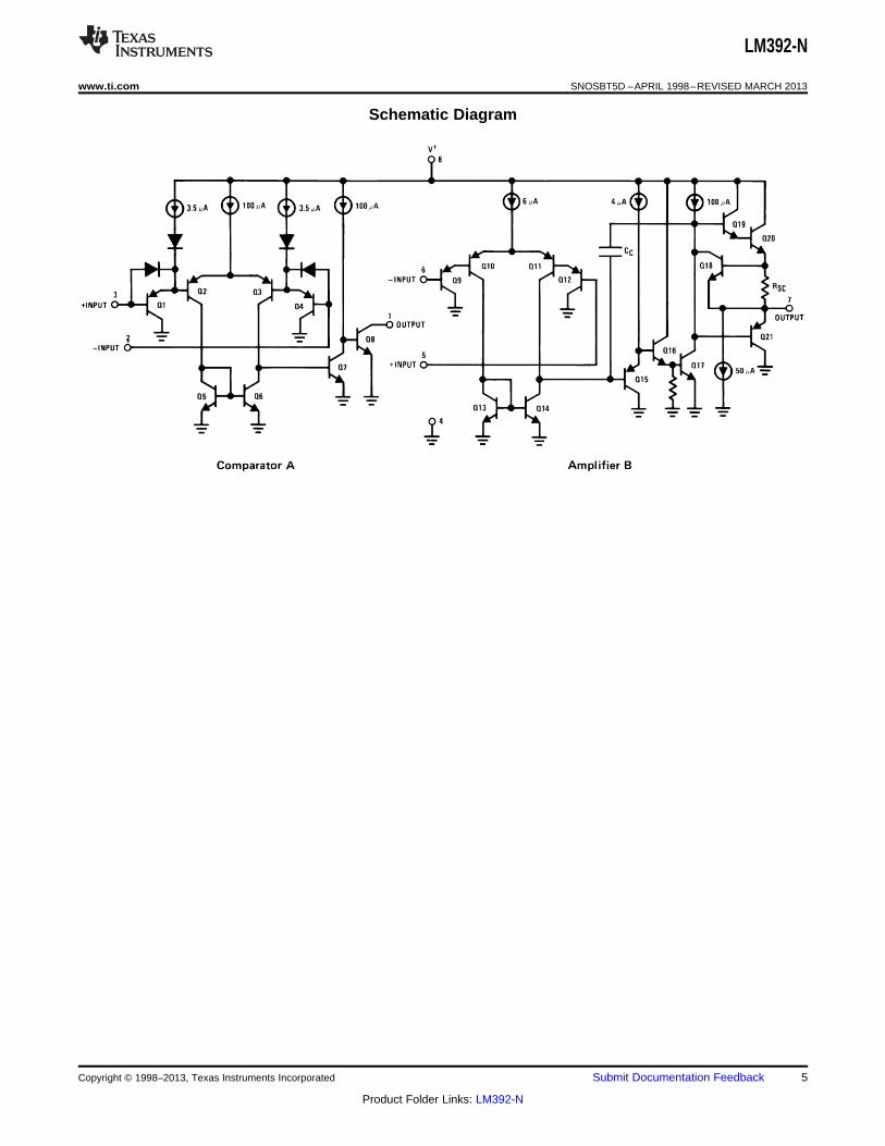
Schematic Diagram
Copyright © 1998–2013, Texas Instruments Incorporated Submit Documentation Feedback 5
Product Folder Links: LM392-N
LM392-N
SNOSBT5D –APRIL 1998–REVISED MARCH 2013 www.ti.com
APPLICATION HINTS
Please refer to the application hints section of the LM193 and the LM158 datasheets.
6 Submit Documentation Feedback Copyright © 1998–2013, Texas Instruments Incorporated
Product Folder Links: LM392-N
LM392-N
www.ti.com SNOSBT5D –APRIL 1998–REVISED MARCH 2013
REVISION HISTORY
Changes from Revision C (March 2013) to Revision D Page
• Changed layout of National Data Sheet to TI format ............................................................................................................ 6
Copyright © 1998–2013, Texas Instruments Incorporated Submit Documentation Feedback 7
Product Folder Links: LM392-N
PACKAGE OPTION ADDENDUM
www.ti.com 30-Sep-2021
Addendum-Page 1
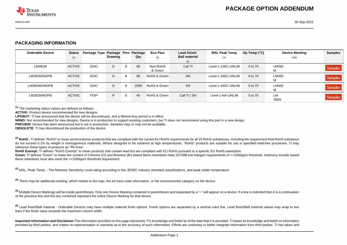
PACKAGING INFORMATION
Orderable Device Status(1)
Package Type PackageDrawing
Pins PackageQty
Eco Plan(2)
Lead finish/Ball material
(6)
MSL Peak Temp(3)
Op Temp (°C) Device Marking(4/5)
Samples
LM392M ACTIVE SOIC D 8 95 Non-RoHS& Green
Call TI Level-1-235C-UNLIM 0 to 70 LM392M
LM392M/NOPB ACTIVE SOIC D 8 95 RoHS & Green SN Level-1-260C-UNLIM 0 to 70 LM392M
LM392MX/NOPB ACTIVE SOIC D 8 2500 RoHS & Green SN Level-1-260C-UNLIM 0 to 70 LM392M
LM392N/NOPB ACTIVE PDIP P 8 40 RoHS & Green Call TI | SN Level-1-NA-UNLIM 0 to 70 LM392N
(1) The marketing status values are defined as follows:ACTIVE: Product device recommended for new designs.LIFEBUY: TI has announced that the device will be discontinued, and a lifetime-buy period is in effect.NRND: Not recommended for new designs. Device is in production to support existing customers, but TI does not recommend using this part in a new design.PREVIEW: Device has been announced but is not in production. Samples may or may not be available.OBSOLETE: TI has discontinued the production of the device.
(2) RoHS: TI defines "RoHS" to mean semiconductor products that are compliant with the current EU RoHS requirements for all 10 RoHS substances, including the requirement that RoHS substancedo not exceed 0.1% by weight in homogeneous materials. Where designed to be soldered at high temperatures, "RoHS" products are suitable for use in specified lead-free processes. TI mayreference these types of products as "Pb-Free".RoHS Exempt: TI defines "RoHS Exempt" to mean products that contain lead but are compliant with EU RoHS pursuant to a specific EU RoHS exemption.Green: TI defines "Green" to mean the content of Chlorine (Cl) and Bromine (Br) based flame retardants meet JS709B low halogen requirements of <=1000ppm threshold. Antimony trioxide basedflame retardants must also meet the <=1000ppm threshold requirement.
(3) MSL, Peak Temp. - The Moisture Sensitivity Level rating according to the JEDEC industry standard classifications, and peak solder temperature.
(4) There may be additional marking, which relates to the logo, the lot trace code information, or the environmental category on the device.
(5) Multiple Device Markings will be inside parentheses. Only one Device Marking contained in parentheses and separated by a "~" will appear on a device. If a line is indented then it is a continuationof the previous line and the two combined represent the entire Device Marking for that device.
(6) Lead finish/Ball material - Orderable Devices may have multiple material finish options. Finish options are separated by a vertical ruled line. Lead finish/Ball material values may wrap to twolines if the finish value exceeds the maximum column width.
Important Information and Disclaimer:The information provided on this page represents TI's knowledge and belief as of the date that it is provided. TI bases its knowledge and belief on informationprovided by third parties, and makes no representation or warranty as to the accuracy of such information. Efforts are underway to better integrate information from third parties. TI has taken and
PACKAGE OPTION ADDENDUM
www.ti.com 30-Sep-2021
Addendum-Page 2
continues to take reasonable steps to provide representative and accurate information but may not have conducted destructive testing or chemical analysis on incoming materials and chemicals.TI and TI suppliers consider certain information to be proprietary, and thus CAS numbers and other limited information may not be available for release.
In no event shall TI's liability arising out of such information exceed the total purchase price of the TI part(s) at issue in this document sold by TI to Customer on an annual basis.
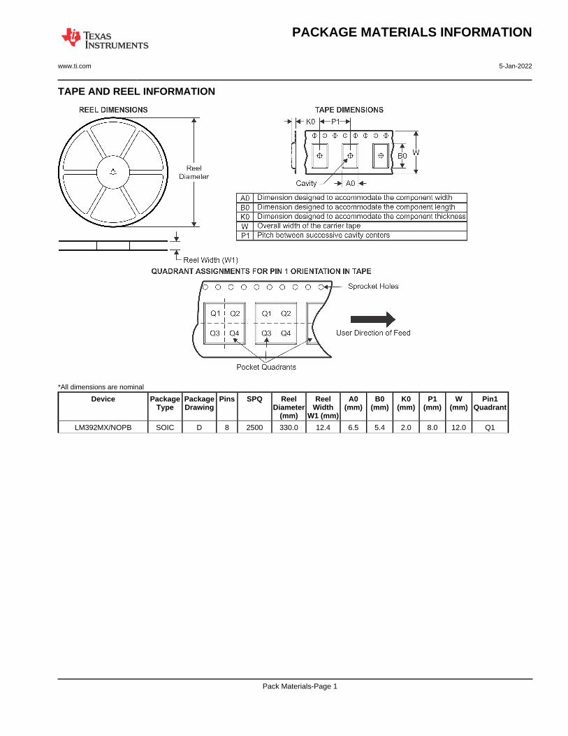
TAPE AND REEL INFORMATION
*All dimensions are nominal
Device PackageType
PackageDrawing
Pins SPQ ReelDiameter
(mm)
ReelWidth
W1 (mm)
A0(mm)
B0(mm)
K0(mm)
P1(mm)
W(mm)
Pin1Quadrant
LM392MX/NOPB SOIC D 8 2500 330.0 12.4 6.5 5.4 2.0 8.0 12.0 Q1
PACKAGE MATERIALS INFORMATION
www.ti.com 5-Jan-2022
Pack Materials-Page 1
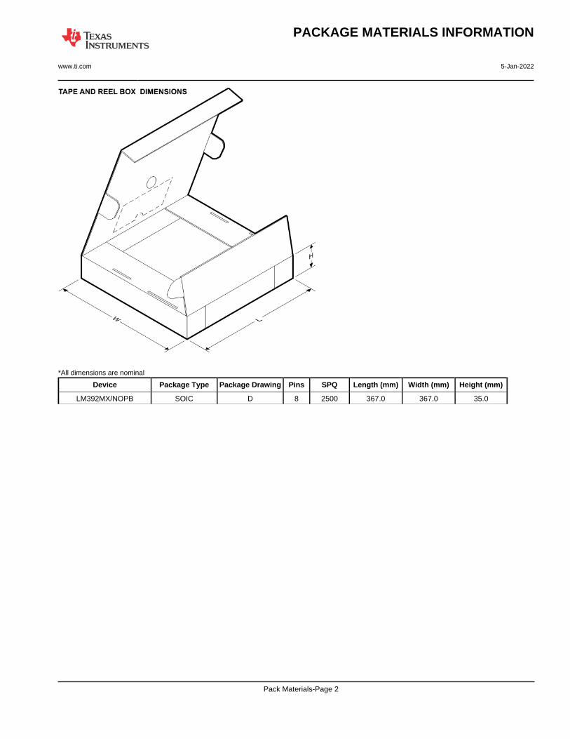
*All dimensions are nominal
Device Package Type Package Drawing Pins SPQ Length (mm) Width (mm) Height (mm)
LM392MX/NOPB SOIC D 8 2500 367.0 367.0 35.0
PACKAGE MATERIALS INFORMATION
www.ti.com 5-Jan-2022
Pack Materials-Page 2
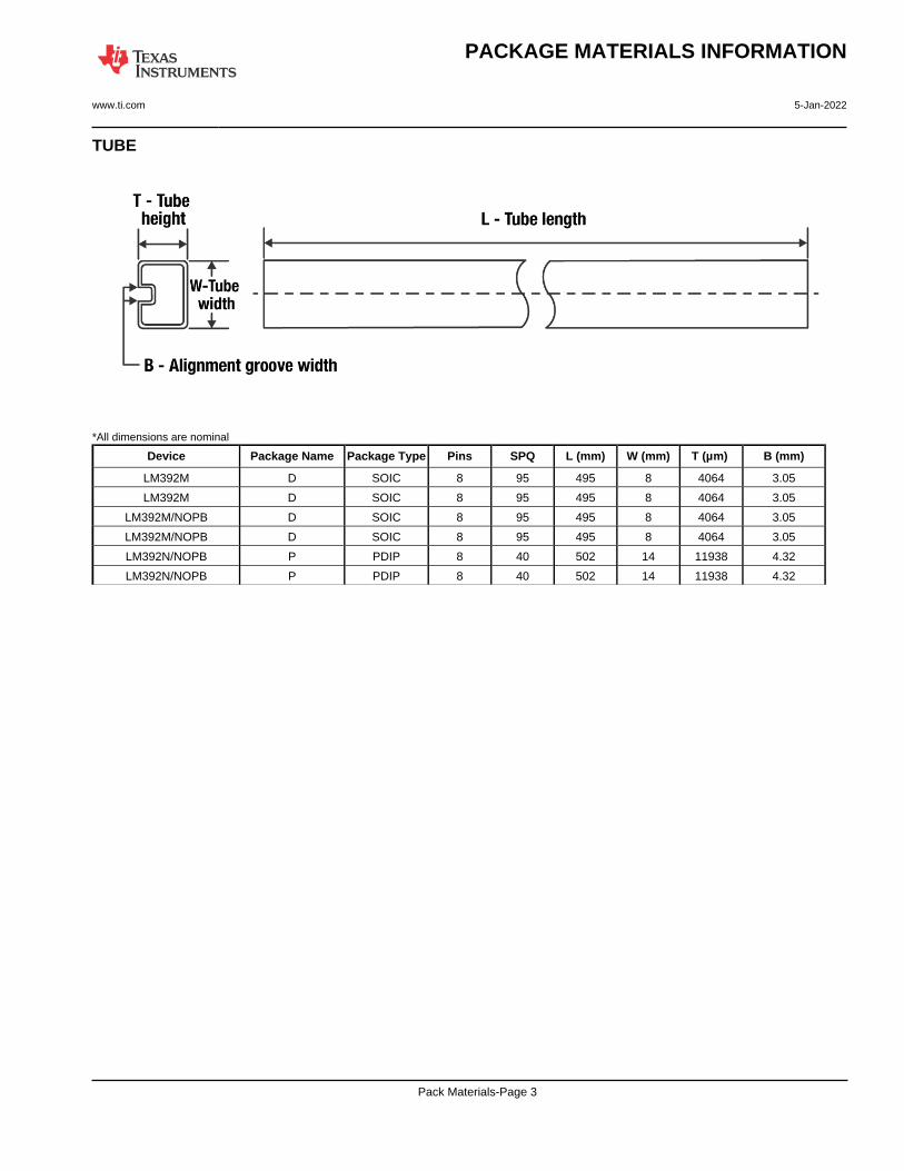
TUBE
*All dimensions are nominal
Device Package Name Package Type Pins SPQ L (mm) W (mm) T (µm) B (mm)
LM392M D SOIC 8 95 495 8 4064 3.05
LM392M D SOIC 8 95 495 8 4064 3.05
LM392M/NOPB D SOIC 8 95 495 8 4064 3.05
LM392M/NOPB D SOIC 8 95 495 8 4064 3.05
LM392N/NOPB P PDIP 8 40 502 14 11938 4.32
LM392N/NOPB P PDIP 8 40 502 14 11938 4.32
PACKAGE MATERIALS INFORMATION
www.ti.com 5-Jan-2022
Pack Materials-Page 3
www.ti.com
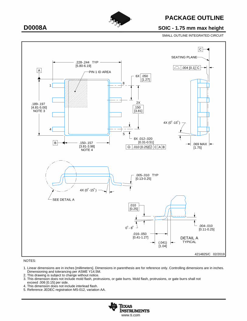
PACKAGE OUTLINE
C
.228-.244 TYP[5.80-6.19]
.069 MAX[1.75]
6X .050[1.27]
8X .012-.020 [0.31-0.51]
2X.150[3.81]
.005-.010 TYP[0.13-0.25]
0 - 8 .004-.010[0.11-0.25]
.010[0.25]
.016-.050[0.41-1.27]
4X (0 -15 )
A
.189-.197[4.81-5.00]
NOTE 3
B .150-.157[3.81-3.98]
NOTE 4
4X (0 -15 )
(.041)[1.04]
SOIC - 1.75 mm max heightD0008ASMALL OUTLINE INTEGRATED CIRCUIT
4214825/C 02/2019
NOTES: 1. Linear dimensions are in inches [millimeters]. Dimensions in parenthesis are for reference only. Controlling dimensions are in inches. Dimensioning and tolerancing per ASME Y14.5M. 2. This drawing is subject to change without notice. 3. This dimension does not include mold flash, protrusions, or gate burrs. Mold flash, protrusions, or gate burrs shall not exceed .006 [0.15] per side. 4. This dimension does not include interlead flash.5. Reference JEDEC registration MS-012, variation AA.
18
.010 [0.25] C A B
54
PIN 1 ID AREA
SEATING PLANE
.004 [0.1] C
SEE DETAIL A
DETAIL ATYPICAL
SCALE 2.800
www.ti.com
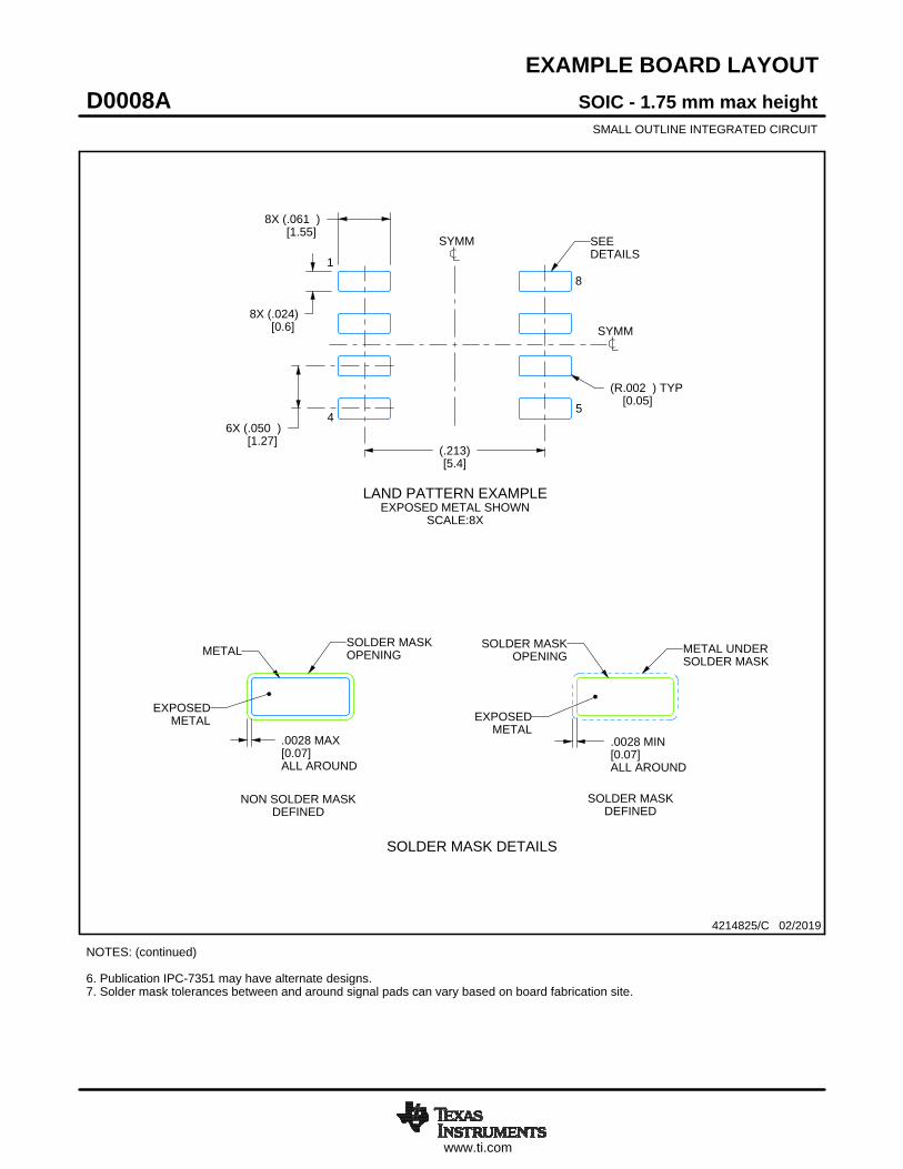
EXAMPLE BOARD LAYOUT
.0028 MAX[0.07]ALL AROUND
.0028 MIN[0.07]ALL AROUND
(.213)[5.4]
6X (.050 )[1.27]
8X (.061 )[1.55]
8X (.024)[0.6]
(R.002 ) TYP[0.05]
SOIC - 1.75 mm max heightD0008ASMALL OUTLINE INTEGRATED CIRCUIT
4214825/C 02/2019
NOTES: (continued) 6. Publication IPC-7351 may have alternate designs. 7. Solder mask tolerances between and around signal pads can vary based on board fabrication site.
METALSOLDER MASKOPENING
NON SOLDER MASKDEFINED
SOLDER MASK DETAILS
EXPOSEDMETAL
OPENINGSOLDER MASK METAL UNDER
SOLDER MASK
SOLDER MASKDEFINED
EXPOSEDMETAL
LAND PATTERN EXAMPLEEXPOSED METAL SHOWN
SCALE:8X
SYMM
1
45
8
SEEDETAILS
SYMM
www.ti.com
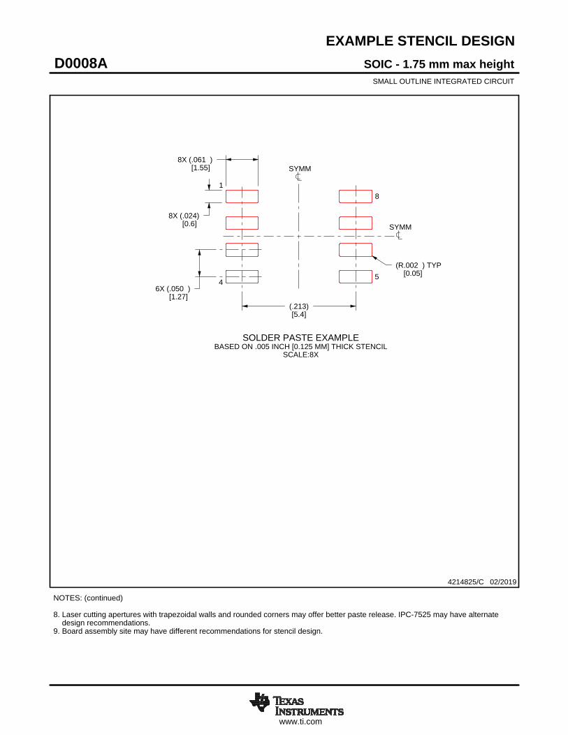
EXAMPLE STENCIL DESIGN
8X (.061 )[1.55]
8X (.024)[0.6]
6X (.050 )[1.27]
(.213)[5.4]
(R.002 ) TYP[0.05]
SOIC - 1.75 mm max heightD0008ASMALL OUTLINE INTEGRATED CIRCUIT
4214825/C 02/2019
NOTES: (continued) 8. Laser cutting apertures with trapezoidal walls and rounded corners may offer better paste release. IPC-7525 may have alternate design recommendations. 9. Board assembly site may have different recommendations for stencil design.
SOLDER PASTE EXAMPLEBASED ON .005 INCH [0.125 MM] THICK STENCIL
SCALE:8X
SYMM
SYMM
1
45
8
IMPORTANT NOTICE AND DISCLAIMERTI PROVIDES TECHNICAL AND RELIABILITY DATA (INCLUDING DATA SHEETS), DESIGN RESOURCES (INCLUDING REFERENCE DESIGNS), APPLICATION OR OTHER DESIGN ADVICE, WEB TOOLS, SAFETY INFORMATION, AND OTHER RESOURCES “AS IS” AND WITH ALL FAULTS, AND DISCLAIMS ALL WARRANTIES, EXPRESS AND IMPLIED, INCLUDING WITHOUT LIMITATION ANY IMPLIED WARRANTIES OF MERCHANTABILITY, FITNESS FOR A PARTICULAR PURPOSE OR NON-INFRINGEMENT OF THIRD PARTY INTELLECTUAL PROPERTY RIGHTS.These resources are intended for skilled developers designing with TI products. You are solely responsible for (1) selecting the appropriate TI products for your application, (2) designing, validating and testing your application, and (3) ensuring your application meets applicable standards, and any other safety, security, regulatory or other requirements.These resources are subject to change without notice. TI grants you permission to use these resources only for development of an application that uses the TI products described in the resource. Other reproduction and display of these resources is prohibited. No license is granted to any other TI intellectual property right or to any third party intellectual property right. TI disclaims responsibility for, and you will fully indemnify TI and its representatives against, any claims, damages, costs, losses, and liabilities arising out of your use of these resources.TI’s products are provided subject to TI’s Terms of Sale or other applicable terms available either on ti.com or provided in conjunction with such TI products. TI’s provision of these resources does not expand or otherwise alter TI’s applicable warranties or warranty disclaimers for TI products.TI objects to and rejects any additional or different terms you may have proposed. IMPORTANT NOTICE
Mailing Address: Texas Instruments, Post Office Box 655303, Dallas, Texas 75265Copyright © 2022, Texas Instruments Incorporated
Recommended