TRANSISTOR BIASING
The steady state operation of a transistor depends a great deal on its base current, collector voltage, and collector current values and therefore, if the transistor is to operate correctly as a linear amplifier, it must be properly biased around its operating point.
Establishing the correct operating point requires the selection of bias resistors and load resistors to provide the appropriate input current and collector voltage conditions. The correct biasing point for a bipolar transistor, either NPN or PNP, generally lies somewhere between the two extremes of operation with respect to it being either “fully-ON” or “fully-OFF” along its DC load line. This central operating point is called the “Quiescent Operating Point”, or Q-point for short.
When a bipolar transistor is biased so that the Q-point is near the middle of its operating range, that is approximately halfway between cut-off and saturation, it is said to be operating as a Class-A amplifier. This mode of operation allows the output voltage to increase and decrease around the amplifiers Q-point without distortion as the input signal swings through one complete cycle. In other words, the output is available for the full 360o of the input cycle.
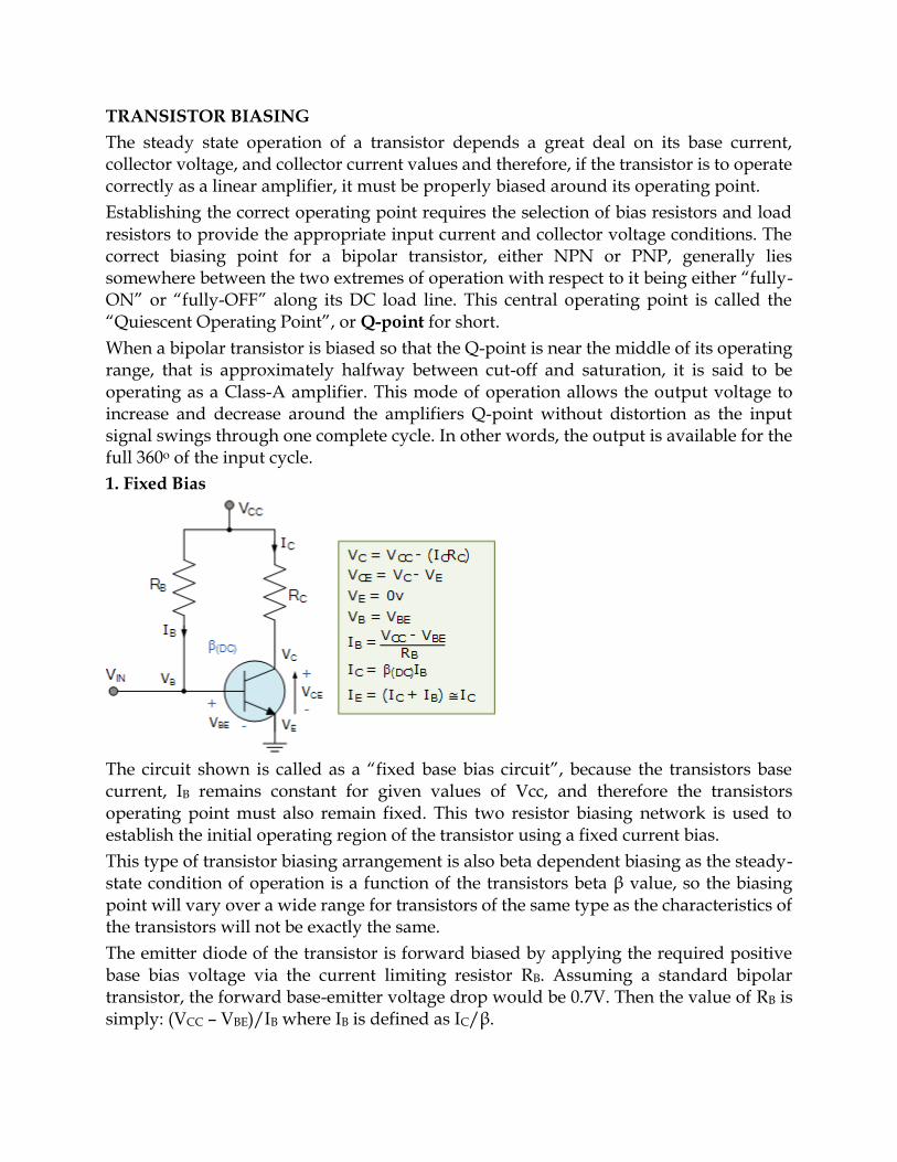
1. Fixed Bias
The circuit shown is called as a “fixed base bias circuit”, because the transistors base current, IB remains constant for given values of Vcc, and therefore the transistors operating point must also remain fixed. This two resistor biasing network is used to establish the initial operating region of the transistor using a fixed current bias.
This type of transistor biasing arrangement is also beta dependent biasing as the steady-state condition of operation is a function of the transistors beta β value, so the biasing point will vary over a wide range for transistors of the same type as the characteristics of the transistors will not be exactly the same.
The emitter diode of the transistor is forward biased by applying the required positive base bias voltage via the current limiting resistor RB. Assuming a standard bipolar transistor, the forward base-emitter voltage drop would be 0.7V. Then the value of RB is simply: (VCC – VBE)/IB where IB is defined as IC/β.
With this single resistor type of biasing arrangement the biasing voltages and currents do not remain stable during transistor operation and can vary enormously. Also the operating temperature of the transistor can adversely affect the operating point.
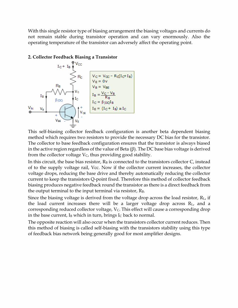
2. Collector Feedback Biasing a Transistor
This self-biasing collector feedback configuration is another beta dependent biasing method which requires two resistors to provide the necessary DC bias for the transistor. The collector to base feedback configuration ensures that the transistor is always biased in the active region regardless of the value of Beta (β). The DC base bias voltage is derived from the collector voltage VC, thus providing good stability.
In this circuit, the base bias resistor, RB is connected to the transistors collector C, instead of to the supply voltage rail, Vcc. Now if the collector current increases, the collector voltage drops, reducing the base drive and thereby automatically reducing the collector current to keep the transistors Q-point fixed. Therefore this method of collector feedback biasing produces negative feedback round the transistor as there is a direct feedback from the output terminal to the input terminal via resistor, RB.
Since the biasing voltage is derived from the voltage drop across the load resistor, RL, if the load current increases there will be a larger voltage drop across RL, and a corresponding reduced collector voltage, VC. This effect will cause a corresponding drop in the base current, IB which in turn, brings IC back to normal.
The opposite reaction will also occur when the transistors collector current reduces. Then this method of biasing is called self-biasing with the transistors stability using this type of feedback bias network being generally good for most amplifier designs.
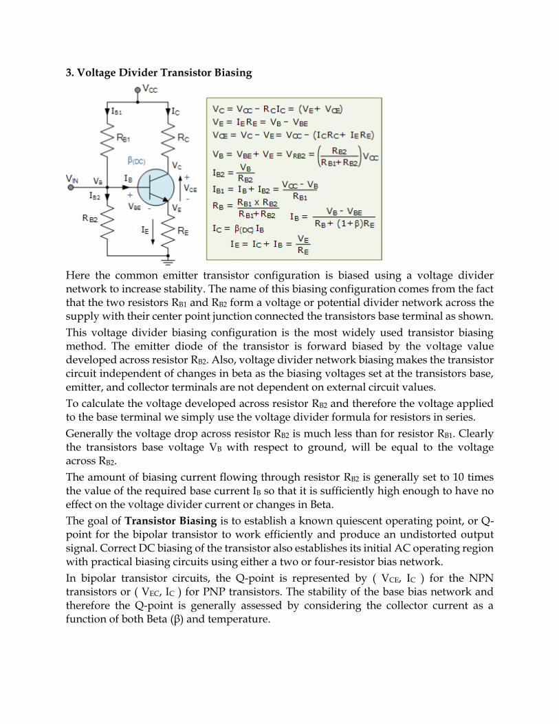
3. Voltage Divider Transistor Biasing
Here the common emitter transistor configuration is biased using a voltage divider network to increase stability. The name of this biasing configuration comes from the fact that the two resistors RB1 and RB2 form a voltage or potential divider network across the supply with their center point junction connected the transistors base terminal as shown.
This voltage divider biasing configuration is the most widely used transistor biasing method. The emitter diode of the transistor is forward biased by the voltage value developed across resistor RB2. Also, voltage divider network biasing makes the transistor circuit independent of changes in beta as the biasing voltages set at the transistors base, emitter, and collector terminals are not dependent on external circuit values.
To calculate the voltage developed across resistor RB2 and therefore the voltage applied to the base terminal we simply use the voltage divider formula for resistors in series.
Generally the voltage drop across resistor RB2 is much less than for resistor RB1. Clearly the transistors base voltage VB with respect to ground, will be equal to the voltage across RB2.
The amount of biasing current flowing through resistor RB2 is generally set to 10 times the value of the required base current IB so that it is sufficiently high enough to have no effect on the voltage divider current or changes in Beta.
The goal of Transistor Biasing is to establish a known quiescent operating point, or Q-point for the bipolar transistor to work efficiently and produce an undistorted output signal. Correct DC biasing of the transistor also establishes its initial AC operating region with practical biasing circuits using either a two or four-resistor bias network.
In bipolar transistor circuits, the Q-point is represented by ( VCE, IC ) for the NPN transistors or ( VEC, IC ) for PNP transistors. The stability of the base bias network and therefore the Q-point is generally assessed by considering the collector current as a function of both Beta (β) and temperature.
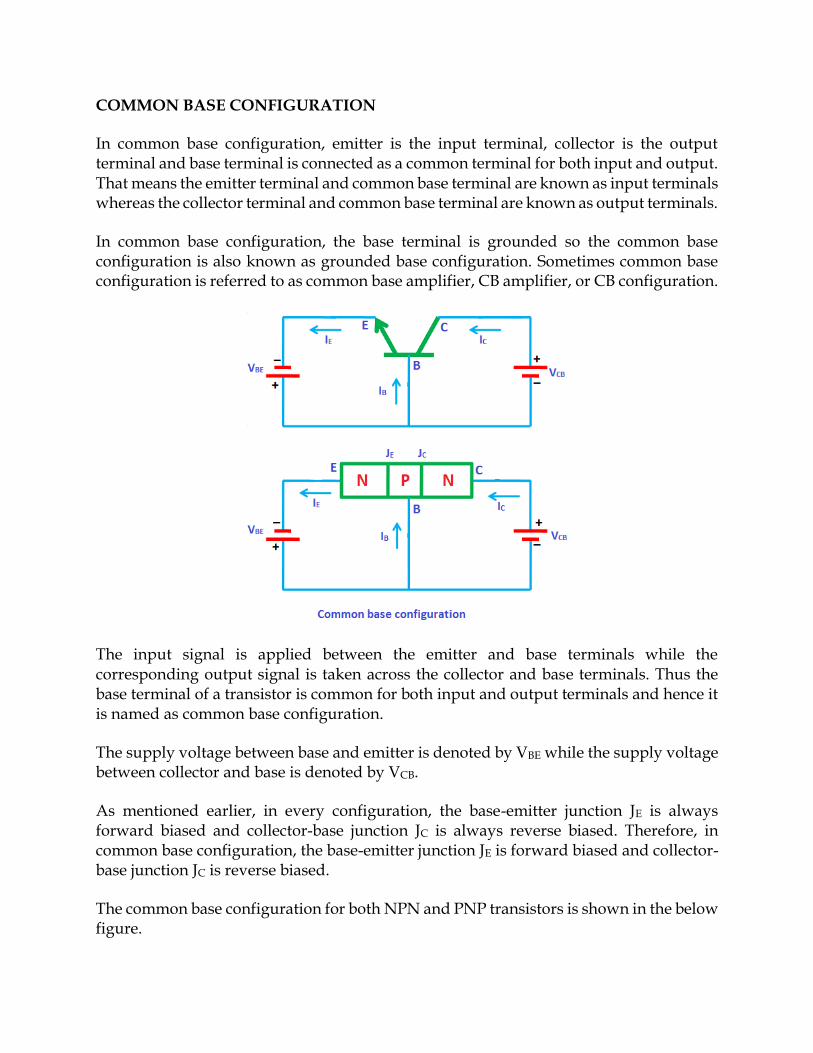
COMMON BASE CONFIGURATION
In common base configuration, emitter is the input terminal, collector is the output terminal and base terminal is connected as a common terminal for both input and output. That means the emitter terminal and common base terminal are known as input terminals whereas the collector terminal and common base terminal are known as output terminals.
In common base configuration, the base terminal is grounded so the common base configuration is also known as grounded base configuration. Sometimes common base configuration is referred to as common base amplifier, CB amplifier, or CB configuration.
The input signal is applied between the emitter and base terminals while the corresponding output signal is taken across the collector and base terminals. Thus the base terminal of a transistor is common for both input and output terminals and hence it is named as common base configuration.
The supply voltage between base and emitter is denoted by VBE while the supply voltage between collector and base is denoted by VCB.
As mentioned earlier, in every configuration, the base-emitter junction JE is always forward biased and collector-base junction JC is always reverse biased. Therefore, in common base configuration, the base-emitter junction JE is forward biased and collector-base junction JC is reverse biased.
The common base configuration for both NPN and PNP transistors is shown in the below figure.
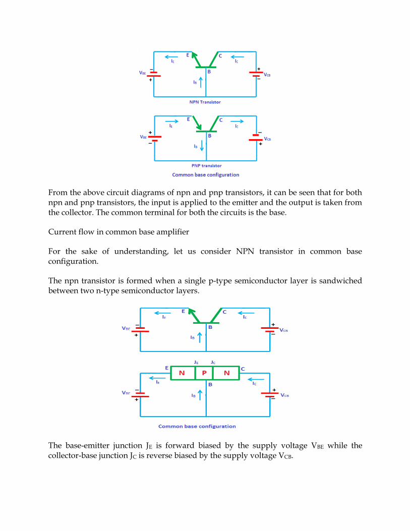
From the above circuit diagrams of npn and pnp transistors, it can be seen that for both npn and pnp transistors, the input is applied to the emitter and the output is taken from the collector. The common terminal for both the circuits is the base.
Current flow in common base amplifier
For the sake of understanding, let us consider NPN transistor in common base configuration.
The npn transistor is formed when a single p-type semiconductor layer is sandwiched between two n-type semiconductor layers.
The base-emitter junction JE is forward biased by the supply voltage VBE while the collector-base junction JC is reverse biased by the supply voltage VCB.
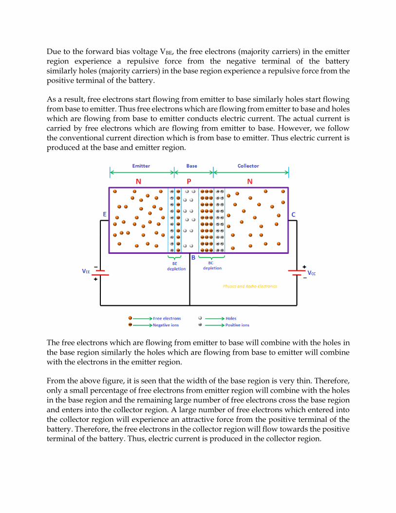
Due to the forward bias voltage VBE, the free electrons (majority carriers) in the emitter region experience a repulsive force from the negative terminal of the battery similarly holes (majority carriers) in the base region experience a repulsive force from the positive terminal of the battery.
As a result, free electrons start flowing from emitter to base similarly holes start flowing from base to emitter. Thus free electrons which are flowing from emitter to base and holes which are flowing from base to emitter conducts electric current. The actual current is carried by free electrons which are flowing from emitter to base. However, we follow the conventional current direction which is from base to emitter. Thus electric current is produced at the base and emitter region.
The free electrons which are flowing from emitter to base will combine with the holes in the base region similarly the holes which are flowing from base to emitter will combine with the electrons in the emitter region.
From the above figure, it is seen that the width of the base region is very thin. Therefore, only a small percentage of free electrons from emitter region will combine with the holes in the base region and the remaining large number of free electrons cross the base region and enters into the collector region. A large number of free electrons which entered into the collector region will experience an attractive force from the positive terminal of the battery. Therefore, the free electrons in the collector region will flow towards the positive terminal of the battery. Thus, electric current is produced in the collector region.
The electric current produced at the collector region is primarily due to the free electrons from the emitter region similarly the electric current produced at the base region is also primarily due to the free electrons from emitter region. Therefore, the emitter current is greater than the base current and collector current. The emitter current is the sum of base current and collector current.
IE = IB + IC
We know that emitter current is the input current and collector current is the output current.
The output collector current is less than the input emitter current, so the current gain of this amplifier is actually less than 1. In other words, the common base amplifier attenuates the electric current rather than amplifying it.
The base-emitter junction JE at input side acts as a forward biased diode. So the common base amplifier has a low input impedance (low opposition to incoming current). On the other hand, the collector-base junction JC at output side acts somewhat like a reverse biased diode. So the common base amplifier has high output impedance.
Therefore, the common base amplifier provides a low input impedance and high output impedance.
Transistors with low input impedance and high output impedance provide a high voltage gain.
Even though the voltage gain is high, the current gain is very low and the overall power gain of the common base amplifier is low as compared to the other transistor amplifier configurations.
The common base transistor amplifiers are primarily used in the applications where low input impedance is required.
The common base amplifier is mainly used as a voltage amplifier or current buffer.
This type of transistor arrangement is not very common and is not as widely used as the other two transistor configurations.
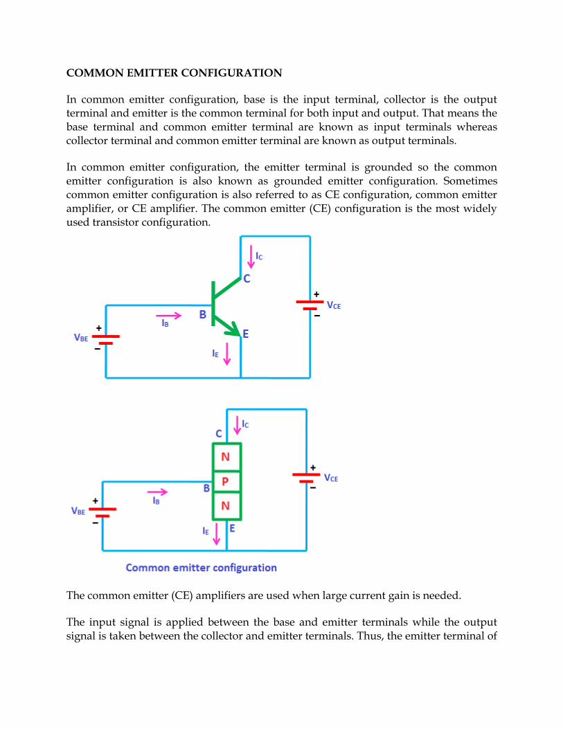
COMMON EMITTER CONFIGURATION
In common emitter configuration, base is the input terminal, collector is the output terminal and emitter is the common terminal for both input and output. That means the base terminal and common emitter terminal are known as input terminals whereas collector terminal and common emitter terminal are known as output terminals.
In common emitter configuration, the emitter terminal is grounded so the common emitter configuration is also known as grounded emitter configuration. Sometimes common emitter configuration is also referred to as CE configuration, common emitter amplifier, or CE amplifier. The common emitter (CE) configuration is the most widely used transistor configuration.
The common emitter (CE) amplifiers are used when large current gain is needed.
The input signal is applied between the base and emitter terminals while the output signal is taken between the collector and emitter terminals. Thus, the emitter terminal of
a transistor is common for both input and output and hence it is named as common emitter configuration.
The supply voltage between base and emitter is denoted by VBE while the supply voltage between collector and emitter is denoted by VCE.
In common emitter (CE) configuration, input current or base current is denoted by IB and output current or collector current is denoted by IC.
The common emitter amplifier has medium input and output impedance levels. So the current gain and voltage gain of the common emitter amplifier is medium. However, the power gain is high.
To fully describe the behavior of a transistor with CE configuration, we need two set of characteristics – input characteristics and output characteristics.
Input characteristics
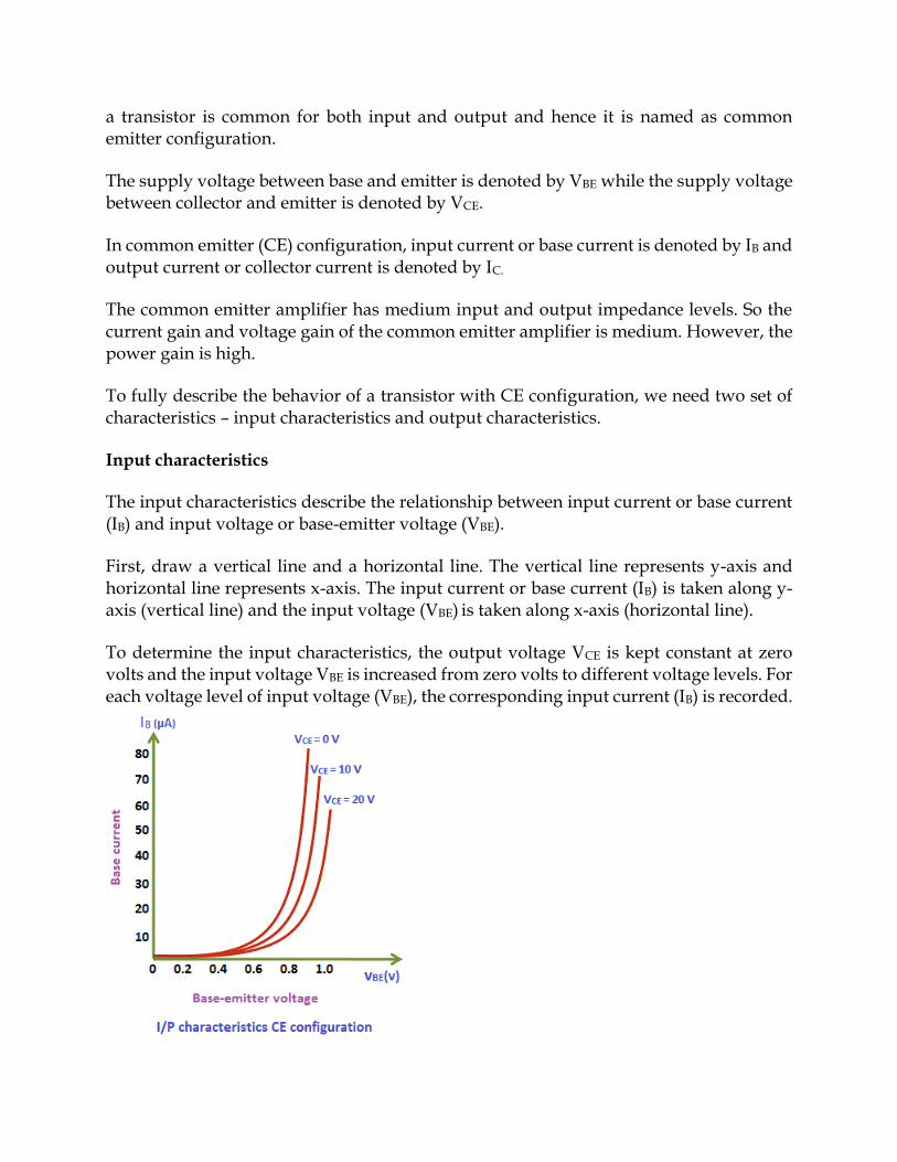
The input characteristics describe the relationship between input current or base current (IB) and input voltage or base-emitter voltage (VBE).
First, draw a vertical line and a horizontal line. The vertical line represents y-axis and horizontal line represents x-axis. The input current or base current (IB) is taken along y-axis (vertical line) and the input voltage (VBE) is taken along x-axis (horizontal line).
To determine the input characteristics, the output voltage VCE is kept constant at zero volts and the input voltage VBE is increased from zero volts to different voltage levels. For each voltage level of input voltage (VBE), the corresponding input current (IB) is recorded.
A curve is then drawn between input current IB and input voltage VBE at constant output voltage VCE (0 volts).
Next, the output voltage (VCE) is increased from zero volts to certain voltage level (10 volts) and the output voltage (VCE) is kept constant at 10 volts. While increasing the output voltage (VCE), the input voltage (VBE) is kept constant at zero volts. After we kept the output voltage (VCE) constant at 10 volts, the input voltage VBE is increased from zero volts to different voltage levels. For each voltage level of input voltage (VBE), the corresponding input current (IB) is recorded.
A curve is then drawn between input current IB and input voltage VBE at constant output voltage VCE (10 volts).
This process is repeated for higher fixed values of output voltage (VCE).
When output voltage (VCE) is at zero volts and emitter-base junction is forward biased by input voltage (VBE), the emitter-base junction acts like a normal p-n junction diode. So the input characteristics of the CE configuration is same as the characteristics of a normal pn junction diode.
The cut in voltage of a silicon transistor is 0.7 volts and germanium transistor is 0.3 volts. In our case, it is a silicon transistor. So from the above graph, we can see that after 0.7 volts, a small increase in input voltage (VBE) will rapidly increases the input current (IB).
In common emitter (CE) configuration, the input current (IB) is very small as compared to the input current (IE) in common base (CB) configuration. The input current in CE configuration is measured in microamperes (μA) whereas the input current in CB configuration is measured in milliamperes (mA).
In common emitter (CE) configuration, the input current (IB) is produced in the base region which is lightly doped and has small width. So the base region produces only a small input current (IB). On the other hand, in common base (CB) configuration, the input current (IE) is produced in the emitter region which is heavily doped and has large width. So the emitter region produces a large input current (IE). Therefore, the input current (IB) produced in the common emitter (CE) configuration is small as compared to the common base (CB) configuration.
Due to forward bias, the emitter-base junction acts as a forward biased diode and due to reverse bias, the collector-base junction acts as a reverse biased diode.
Therefore, the width of the depletion region at the emitter-base junction is very small whereas the width of the depletion region at the collector-base junction is very large.
If the output voltage VCE applied to the collector-base junction is further increased, the depletion region width further increases. The base region is lightly doped as compared to the collector region. So the depletion region penetrates more into the base region and less into the collector region. As a result, the width of the base region decreases which in turn reduces the input current (IB) produced in the base region.
From the above characteristics, we can see that for higher fixed values of output voltage VCE, the curve shifts to the right side. This is because for higher fixed values of output voltage, the cut in voltage is increased above 0.7 volts. Therefore, to overcome this cut in voltage, more input voltage VBE is needed than previous case.
Output characteristics
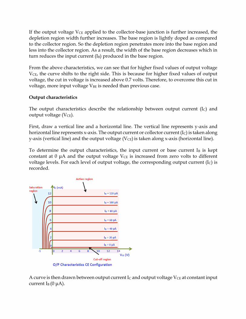
The output characteristics describe the relationship between output current (IC) and output voltage (VCE).
First, draw a vertical line and a horizontal line. The vertical line represents y-axis and horizontal line represents x-axis. The output current or collector current (IC) is taken along y-axis (vertical line) and the output voltage (VCE) is taken along x-axis (horizontal line).
To determine the output characteristics, the input current or base current IB is kept constant at 0 μA and the output voltage VCE is increased from zero volts to different voltage levels. For each level of output voltage, the corresponding output current (IC) is recorded.
A curve is then drawn between output current IC and output voltage VCE at constant input current IB (0 μA).
When the base current or input current IB = 0 μA, the transistor operates in the cut-off region. In this region, both junctions are reverse biased.
Next, the input current (IB) is increased from 0 μA to 20 μA by adjusting the input voltage (VBE). The input current (IB) is kept constant at 20 μA.
While increasing the input current (IB), the output voltage (VCE) is kept constant at 0 volts.
After we kept the input current (IB) constant at 20 μA, the output voltage (VCE) is increased from zero volts to different voltage levels. For each voltage level of output voltage (VCE), the corresponding output current (IC) is recorded.
A curve is then drawn between output current IC and output voltage VCE at constant input current IB (20 μA). This region is known as the active region of a transistor. In this region, emitter-base junction is forward biased and the collector-base junction is reverse biased.
This steps are repeated for higher fixed values of input current IB (I.e. 40 μA, 60 μA, 80 μA and so on).
When output voltage VCE is reduced to a small value (0.2 V), the collector-base junction becomes forward biased. This is because the output voltage VCE has less effect on collector-base junction than input voltage VBE.
As we know that the emitter-base junction is already forward biased. Therefore, when both the junctions are forward biased, the transistor operates in the saturation region. In this region, a small increase in output voltage VCE will rapidly increases the output current IC.
Transistor parameters
Dynamic input resistance (ri)
Dynamic input resistance is defined as the ratio of change in input voltage or base voltage (VBE) to the corresponding change in input current or base current (IB), with the output voltage or collector voltage (VCE) kept at constant.
In CE configuration, the input resistance is very low.
Dynamic output resistance (ro) Dynamic output resistance is defined as the ratio of change in output voltage or collector voltage (VCE) to the corresponding change in output current or collector
current (IC), with the input current or base current (IB) kept at constant.
In CE configuration, the output resistance is high.
Current gain (α)
The current gain of a transistor in CE configuration is defined as the ratio of output current or collector current (IC) to the input current or base current (IB).
The current gain of a transistor in CE configuration is high. Therefore, the transistor in CE configuration is used for amplifying the current.
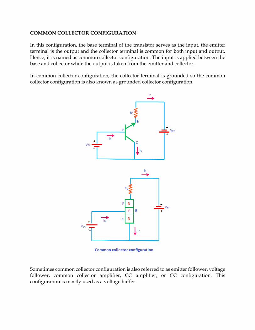
COMMON COLLECTOR CONFIGURATION
In this configuration, the base terminal of the transistor serves as the input, the emitter terminal is the output and the collector terminal is common for both input and output. Hence, it is named as common collector configuration. The input is applied between the base and collector while the output is taken from the emitter and collector.
In common collector configuration, the collector terminal is grounded so the common collector configuration is also known as grounded collector configuration.
Sometimes common collector configuration is also referred to as emitter follower, voltage follower, common collector amplifier, CC amplifier, or CC configuration. This configuration is mostly used as a voltage buffer.
The input supply voltage between base and collector is denoted by VBC while the output voltage between emitter and collector is denoted by VEC.
In this configuration, input current or base current is denoted by IB and output current or emitter current is denoted by IE.The common collector amplifier has high input impedance and low output impedance. It has low voltage gain and high current gain.
The power gain of the common collector amplifier is medium. To fully describe the behavior of a transistor with CC configuration, we need two set of characteristics - input characteristics and output characteristics.
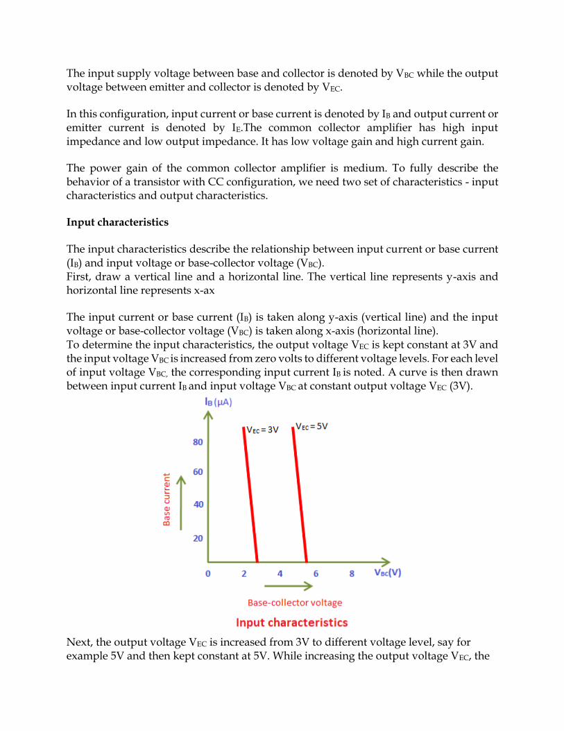
Input characteristics The input characteristics describe the relationship between input current or base current (IB) and input voltage or base-collector voltage (VBC). First, draw a vertical line and a horizontal line. The vertical line represents y-axis and horizontal line represents x-ax
The input current or base current (IB) is taken along y-axis (vertical line) and the input voltage or base-collector voltage (VBC) is taken along x-axis (horizontal line). To determine the input characteristics, the output voltage VEC is kept constant at 3V and the input voltage VBC is increased from zero volts to different voltage levels. For each level of input voltage VBC, the corresponding input current IB is noted. A curve is then drawn between input current IB and input voltage VBC at constant output voltage VEC (3V).
Next, the output voltage VEC is increased from 3V to different voltage level, say for example 5V and then kept constant at 5V. While increasing the output voltage VEC, the
input voltage VBC is kept constant at zero volts.
After we kept the output voltage VEC constant at 5V, the input voltage VBC is increased from zero volts to different voltage levels. For each level of input voltage VBC, the corresponding input current IB is noted. A curve is then drawn between input current IB
and input voltage VBC at constant output voltage VEC (5V).
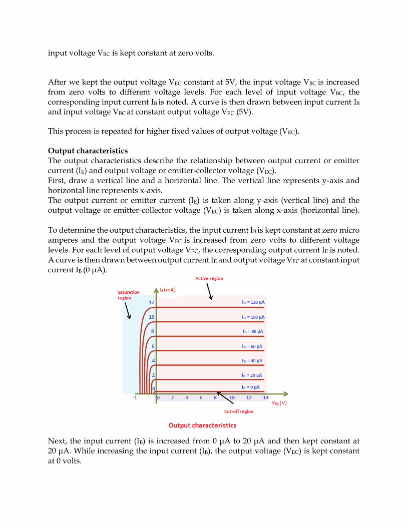
This process is repeated for higher fixed values of output voltage (VEC). Output characteristics The output characteristics describe the relationship between output current or emitter current (IE) and output voltage or emitter-collector voltage (VEC). First, draw a vertical line and a horizontal line. The vertical line represents y-axis and horizontal line represents x-axis. The output current or emitter current (IE) is taken along y-axis (vertical line) and the output voltage or emitter-collector voltage (VEC) is taken along x-axis (horizontal line). To determine the output characteristics, the input current IB is kept constant at zero micro amperes and the output voltage VEC is increased from zero volts to different voltage levels. For each level of output voltage VEC, the corresponding output current IE is noted. A curve is then drawn between output current IE and output voltage VEC at constant input current IB (0 μA).
Next, the input current (IB) is increased from 0 μA to 20 μA and then kept constant at 20 μA. While increasing the input current (IB), the output voltage (VEC) is kept constant at 0 volts.
After we kept the input current (IB) constant at 20 μA, the output voltage (VEC) is increased from zero volts to different voltage levels. For each level of output voltage (VEC), the corresponding output current (IE) is recorded. A curve is then drawn between output current IE and output voltage VEC at constant input current IB (20μA). This region is known as the active region of a transistor. This process is repeated for higher fixed values of input current IB (I.e. 40 μA, 60 μA, 80 μA and so on). In common collector configuration, if the input current or base current is zero then the output current or emitter current is also zero. As a result, no current flows through the transistor. So the transistor will be in the cutoff region. If the base current is slightly increased then the output current or emitter current also increases. So the transistor falls into the active region. If the base current is heavily increased then the current flowing through the transistor also heavily increases. As a result, the transistor falls into the saturation region. Transistor parameters Dynamic input resistance (ri) Dynamic input resistance is defined as the ratio of change in input voltage or base voltage (VBC) to the corresponding change in input current or base current (IB), with the output voltage or emitter voltage (VEC) kept at constant.
The input resistance of common collector amplifier is high. Dynamic output resistance (ro) Dynamic output resistance is defined as the ratio of change in output voltage or emitter voltage (VEC) to the corresponding change in output current or emitter current (IE), with the input current or base current (IB) kept at constant. The output resistance of common collector amplifier is low.
Current amplification factor (γ) The current amplification factor is defined as the ratio of change in output current or emitter current IE to the change in input current or base current IB. It is expressed by γ.
The current gain of a common collector amplifier is high.
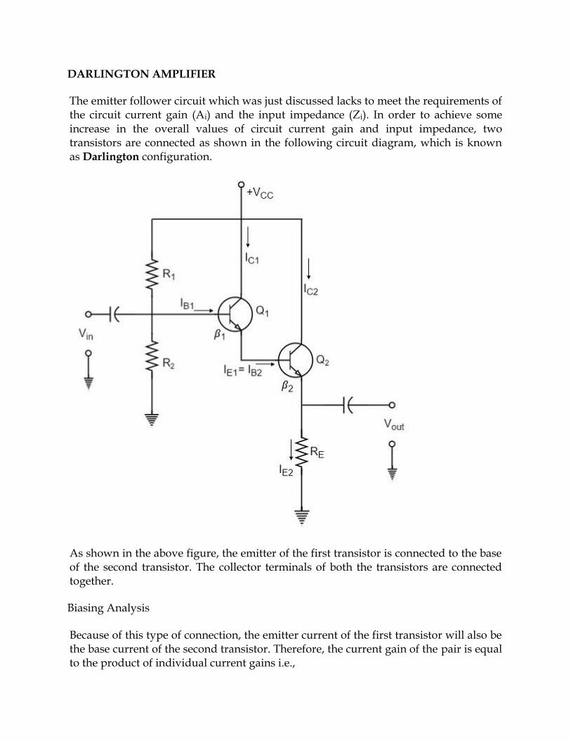
DARLINGTON AMPLIFIER
The emitter follower circuit which was just discussed lacks to meet the requirements of the circuit current gain (Ai) and the input impedance (Zi). In order to achieve some increase in the overall values of circuit current gain and input impedance, two transistors are connected as shown in the following circuit diagram, which is known as Darlington configuration.
As shown in the above figure, the emitter of the first transistor is connected to the base of the second transistor. The collector terminals of both the transistors are connected together.
Biasing Analysis
Because of this type of connection, the emitter current of the first transistor will also be the base current of the second transistor. Therefore, the current gain of the pair is equal to the product of individual current gains i.e.,
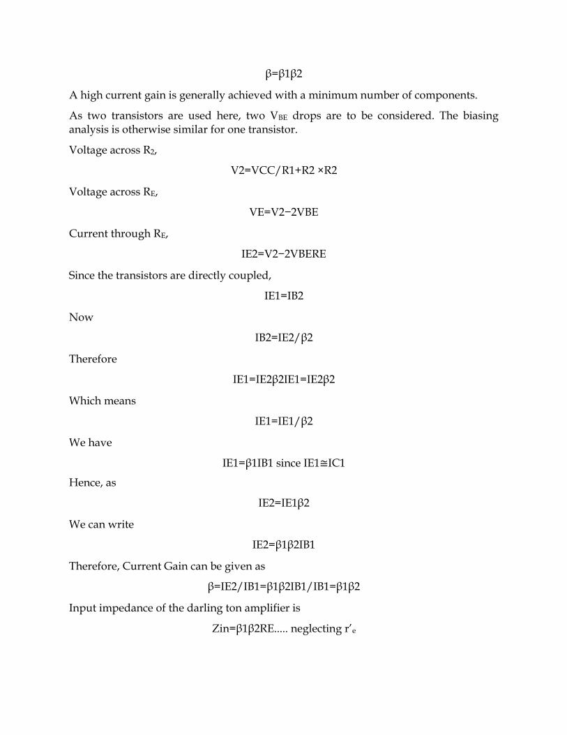
β=β1β2
A high current gain is generally achieved with a minimum number of components.
As two transistors are used here, two VBE drops are to be considered. The biasing analysis is otherwise similar for one transistor.
Voltage across R2,
V2=VCC/R1+R2 ×R2
Voltage across RE,
VE=V2−2VBE
Current through RE,
IE2=V2−2VBERE
Since the transistors are directly coupled,
IE1=IB2
Now
IB2=IE2/β2
Therefore
IE1=IE2β2IE1=IE2β2
Which means
IE1=IE1/β2
We have
IE1=β1IB1 since IE1≅IC1
Hence, as
IE2=IE1β2
We can write
IE2=β1β2IB1
Therefore, Current Gain can be given as
β=IE2/IB1=β1β2IB1/IB1=β1β2
Input impedance of the darling ton amplifier is
Zin=β1β2RE..... neglecting r’e
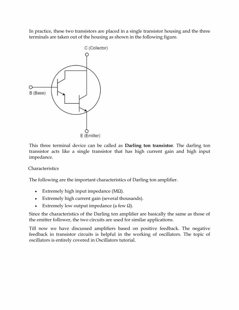
In practice, these two transistors are placed in a single transistor housing and the three terminals are taken out of the housing as shown in the following figure.
This three terminal device can be called as Darling ton transistor. The darling ton transistor acts like a single transistor that has high current gain and high input impedance.
Characteristics
The following are the important characteristics of Darling ton amplifier.
Extremely high input impedance (MΩ).
Extremely high current gain (several thousands).
Extremely low output impedance (a few Ω).
Since the characteristics of the Darling ton amplifier are basically the same as those of the emitter follower, the two circuits are used for similar applications.
Till now we have discussed amplifiers based on positive feedback. The negative feedback in transistor circuits is helpful in the working of oscillators. The topic of oscillators is entirely covered in Oscillators tutorial.
CLASS A POWER AMPLIFIER.
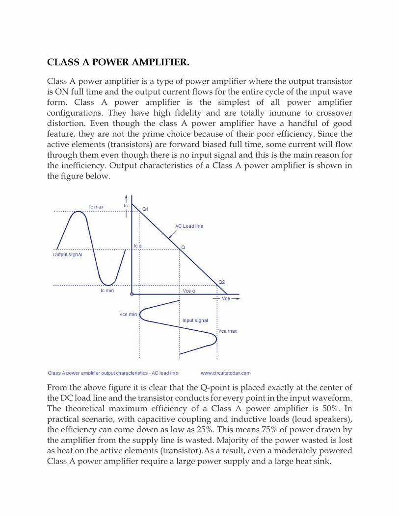
Class A power amplifier is a type of power amplifier where the output transistor is ON full time and the output current flows for the entire cycle of the input wave form. Class A power amplifier is the simplest of all power amplifier configurations. They have high fidelity and are totally immune to crossover distortion. Even though the class A power amplifier have a handful of good feature, they are not the prime choice because of their poor efficiency. Since the active elements (transistors) are forward biased full time, some current will flow through them even though there is no input signal and this is the main reason for the inefficiency. Output characteristics of a Class A power amplifier is shown in the figure below.
From the above figure it is clear that the Q-point is placed exactly at the center of the DC load line and the transistor conducts for every point in the input waveform. The theoretical maximum efficiency of a Class A power amplifier is 50%. In practical scenario, with capacitive coupling and inductive loads (loud speakers), the efficiency can come down as low as 25%. This means 75% of power drawn by the amplifier from the supply line is wasted. Majority of the power wasted is lost as heat on the active elements (transistor).As a result, even a moderately powered Class A power amplifier require a large power supply and a large heat sink.
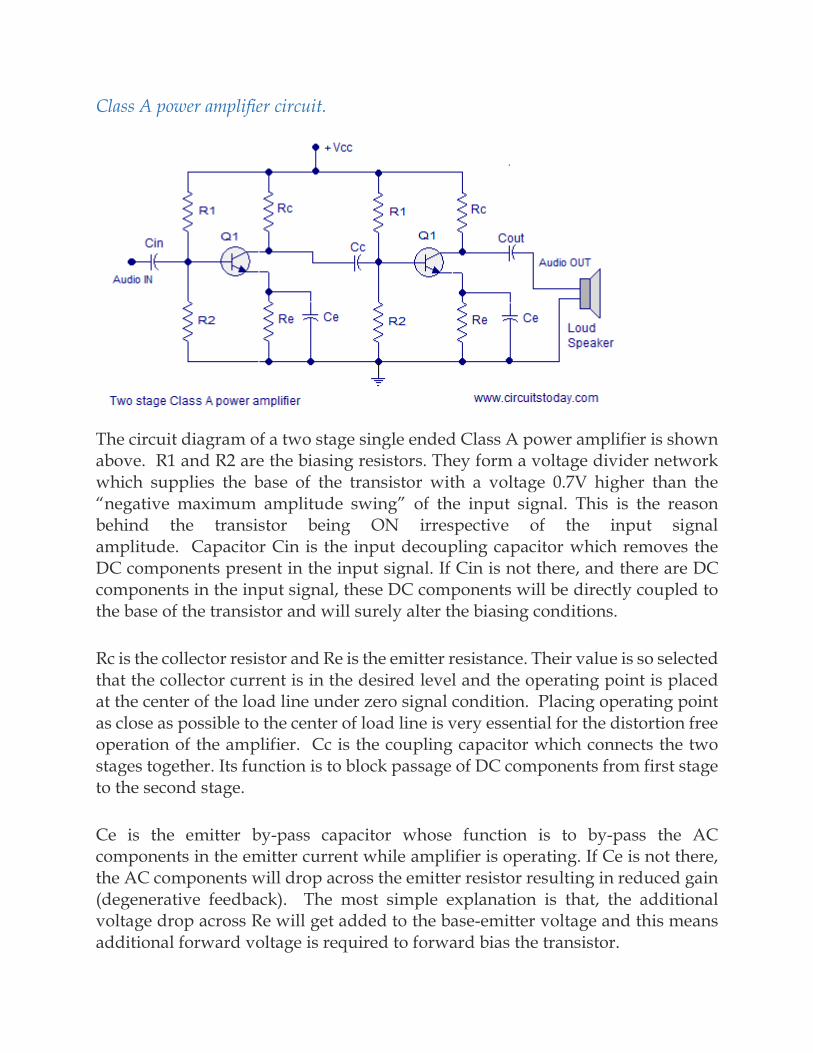
Class A power amplifier circuit.
The circuit diagram of a two stage single ended Class A power amplifier is shown above. R1 and R2 are the biasing resistors. They form a voltage divider network which supplies the base of the transistor with a voltage 0.7V higher than the “negative maximum amplitude swing” of the input signal. This is the reason behind the transistor being ON irrespective of the input signal amplitude. Capacitor Cin is the input decoupling capacitor which removes the DC components present in the input signal. If Cin is not there, and there are DC components in the input signal, these DC components will be directly coupled to the base of the transistor and will surely alter the biasing conditions.
Rc is the collector resistor and Re is the emitter resistance. Their value is so selected that the collector current is in the desired level and the operating point is placed at the center of the load line under zero signal condition. Placing operating point as close as possible to the center of load line is very essential for the distortion free operation of the amplifier. Cc is the coupling capacitor which connects the two stages together. Its function is to block passage of DC components from first stage to the second stage.
Ce is the emitter by-pass capacitor whose function is to by-pass the AC components in the emitter current while amplifier is operating. If Ce is not there, the AC components will drop across the emitter resistor resulting in reduced gain (degenerative feedback). The most simple explanation is that, the additional voltage drop across Re will get added to the base-emitter voltage and this means additional forward voltage is required to forward bias the transistor.
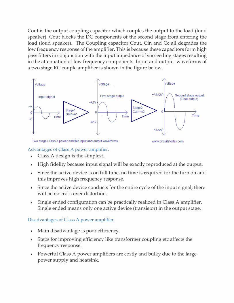
Cout is the output coupling capacitor which couples the output to the load (loud speaker). Cout blocks the DC components of the second stage from entering the load (loud speaker). The Coupling capacitor Cout, Cin and Cc all degrades the low frequency response of the amplifier. This is because these capacitors form high pass filters in conjunction with the input impedance of succeeding stages resulting in the attenuation of low frequency components. Input and output waveforms of a two stage RC couple amplifier is shown in the figure below.
Advantages of Class A power amplifier.
Class A design is the simplest.
High fidelity because input signal will be exactly reproduced at the output.
Since the active device is on full time, no time is required for the turn on and this improves high frequency response.
Since the active device conducts for the entire cycle of the input signal, there will be no cross over distortion.
Single ended configuration can be practically realized in Class A amplifier. Single ended means only one active device (transistor) in the output stage.
Disadvantages of Class A power amplifier.
Main disadvantage is poor efficiency.
Steps for improving efficiency like transformer coupling etc affects the frequency response.
Powerful Class A power amplifiers are costly and bulky due to the large power supply and heatsink.
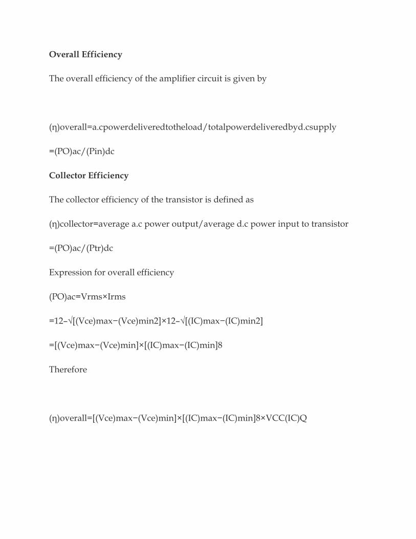
Overall Efficiency
The overall efficiency of the amplifier circuit is given by
(η)overall=a.cpowerdeliveredtotheload/totalpowerdeliveredbyd.csupply
=(PO)ac/(Pin)dc
Collector Efficiency
The collector efficiency of the transistor is defined as
(η)collector=average a.c power output/average d.c power input to transistor
=(PO)ac/(Ptr)dc
Expression for overall efficiency
(PO)ac=Vrms×Irms
=12–√[(Vce)max−(Vce)min2]×12–√[(IC)max−(IC)min2]
=[(Vce)max−(Vce)min]×[(IC)max−(IC)min]8
Therefore
(η)overall=[(Vce)max−(Vce)min]×[(IC)max−(IC)min]8×VCC(IC)Q
CLASS B POWER AMPLIFIER
To improve the full power efficiency of the previous Class A amplifier by reducing the wasted power in the form of heat, it is possible to design the power amplifier circuit with two transistors in its output stage producing what is commonly termed as a Class B Amplifier also known as a push-pull
amplifier configuration.
Push-pull amplifiers use two “complementary” or matching transistors, one being an NPN-type and the other being a PNP-type with both power transistors receiving the same input signal together that is equal in magnitude, but in opposite phase to each other. This results in one transistor only amplifying one half or 180o of the input waveform cycle while the other transistor amplifies the other half or remaining 180o of the input waveform cycle with the resulting “two-halves” being put back together again at the output terminal.
Then the conduction angle for this type of amplifier circuit is only 180o or 50% of the input signal. This pushing and pulling effect of the alternating half cycles by the transistors gives this type of circuit its amusing “push-pull” name, but are more generally known as the Class B Amplifier as shown below.
Class B Push-pull Transformer Amplifier Circuit
The circuit above shows a standard Class B Amplifier circuit that uses a balanced center-tapped input transformer, which splits the incoming waveform signal into two equal halves and which are 180o out of phase with each other. Another center-tapped transformer on the output is used to recombined the two signals providing the increased power to the load. The transistors used for this type of transformer push-pull amplifier circuit are both NPN transistors with their emitter terminals connected together.
Here, the load current is shared between the two power transistor devices as it decreases in one device and increases in the other throughout the signal cycle reducing the output voltage and current to zero. The result is that both halves of the output waveform now swings from zero to twice the quiescent current thereby reducing dissipation. This has the effect of almost doubling the efficiency of the amplifier to around 70%.
Assuming that no input signal is present, then each transistor carries the normal quiescent collector current, the value of which is determined by the base bias which is at the cut-off point. If the transformer is accurately center tapped, then the two collector currents will flow in opposite directions (ideal condition) and there will be no magnetization of the transformer core, thus minimizing the possibility of distortion.
When an input signal is present across the secondary of the driver transformer T1, the transistor base inputs are in “anti-phase” to each other as shown, thus if TR1 base goes positive driving the transistor into heavy conduction, its collector current will increase but at the same time the base current of TR2 will go negative further into cut-off and the collector current of this transistor decreases by an equal amount and vice versa. Hence negative halves are amplified by one transistor and positive halves by the other transistor giving this push-pull effect.
Unlike the DC condition, these alternating currents are ADDITIVE resulting in the two output half-cycles being combined to reform the sine-wave in the output transformers primary winding which then appears across the load.
Class B Amplifier operation has zero DC bias as the transistors are biased at the cut-off, so each transistor only conducts when the input signal is greater than the Base-emitter voltage. Therefore, at zero input there is zero output and no power is being consumed. This then means that the actual Q-point of a Class B amplifier is on the Vce part of the load line as shown below.
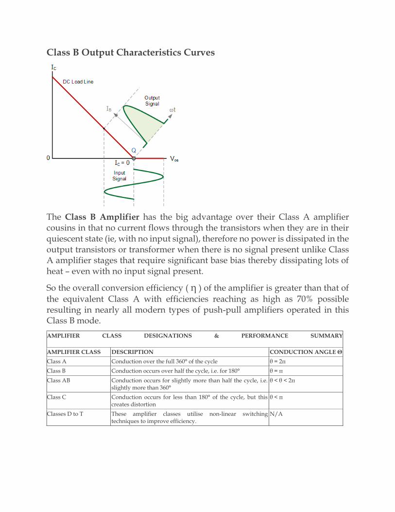
Class B Output Characteristics Curves
The Class B Amplifier has the big advantage over their Class A amplifier cousins in that no current flows through the transistors when they are in their quiescent state (ie, with no input signal), therefore no power is dissipated in the output transistors or transformer when there is no signal present unlike Class A amplifier stages that require significant base bias thereby dissipating lots of heat – even with no input signal present.
So the overall conversion efficiency ( η ) of the amplifier is greater than that of
the equivalent Class A with efficiencies reaching as high as 70% possible resulting in nearly all modern types of push-pull amplifiers operated in this Class B mode.
AMPLIFIER CLASS DESIGNATIONS & PERFORMANCE SUMMARY
AMPLIFIER CLASS DESCRIPTION CONDUCTION ANGLE Θ
Class A Conduction over the full 360° of the cycle θ = 2π
Class B Conduction occurs over half the cycle, i.e. for 180° θ = π
Class AB Conduction occurs for slightly more than half the cycle, i.e. slightly more than 360°
θ < θ < 2π
Class C Conduction occurs for less than 180° of the cycle, but this creates distortion
θ < π
Classes D to T These amplifier classes utilise non-linear switching techniques to improve efficiency.
N/A
Recommended


![Exchange biasing and electric polarization with YMnO[sub 3]](https://img.pdfslide.net/doc/110x75/6351c6da56dfd81308033baf/exchange-biasing-and-electric-polarization-with-ymnosub-3.jpg)


