Embed Size (px)
Citation preview

Characterization of Nanoparticles
Prepared by: Amany F. El-Hallaq
Safia F. Salama
Dr. Issa El-Nahal:Supervisor
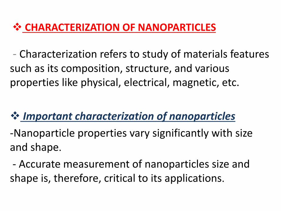
CHARACTERIZATION OF NANOPARTICLES
- Characterization refers to study of materials features such as its composition, structure, and various properties like physical, electrical, magnetic, etc.
Important characterization of nanoparticles
-Nanoparticle properties vary significantly with size .and shape
- Accurate measurement of nanoparticles size and .shape is, therefore, critical to its applications
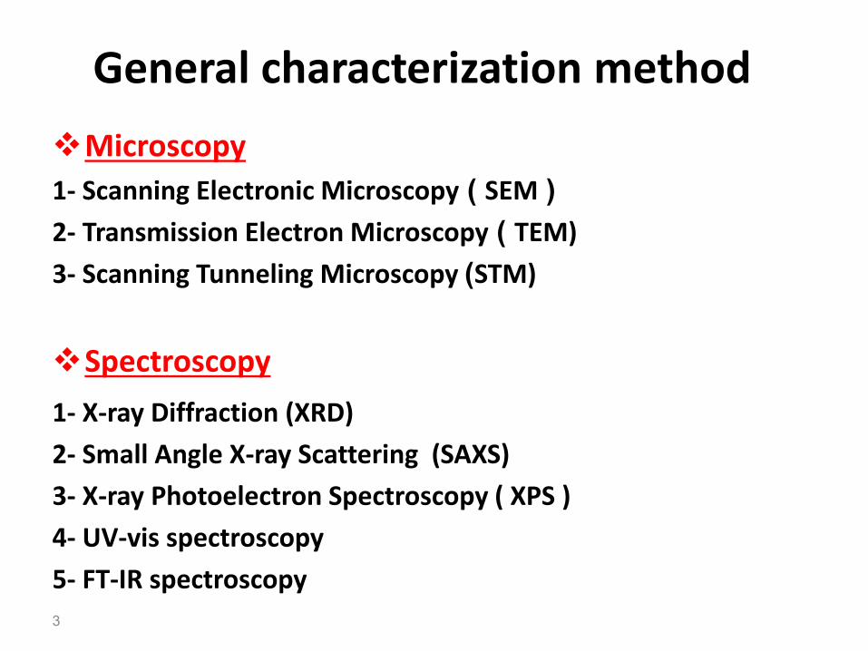
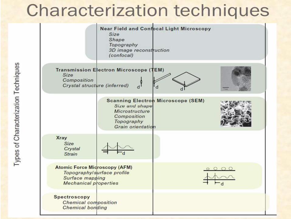
General characterization method
Microscopy
(SEM )1- Scanning Electronic Microscopy
TEM) )2- Transmission Electron Microscopy
STM))3- Scanning Tunneling Microscopy
Spectroscopy
1- X-ray Diffraction (XRD)
2- Small Angle X-ray Scattering (SAXS)
3- X-ray Photoelectron Spectroscopy ( XPS )
4- UV-vis spectroscopy
5- FT-IR spectroscopy
3
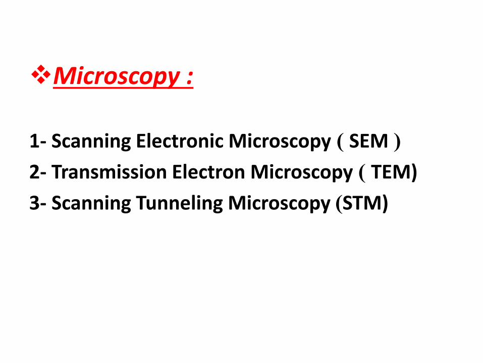
Microscopy :
(SEM)1- Scanning Electronic Microscopy
TEM))2- Transmission Electron Microscopy
STM))3- Scanning Tunneling Microscopy
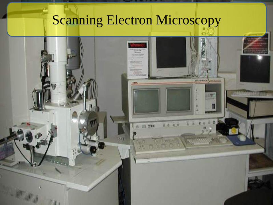
Scanning Electron Microscopy
5
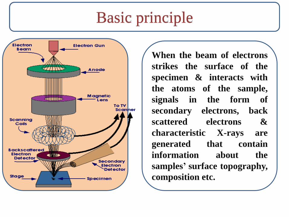
When the beam of electrons
strikes the surface of the
specimen & interacts with
the atoms of the sample,
signals in the form of
secondary electrons, back
scattered electrons &
characteristic X-rays are
generated that contain
information about the
samples’ surface topography,
composition etc.
Basic principle
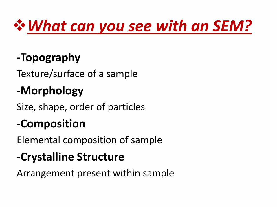
-Topography
Texture/surface of a sample
-Morphology
Size, shape, order of particles
-Composition
Elemental composition of sample
-Crystalline Structure
Arrangement present within sample
What can you see with an SEM?
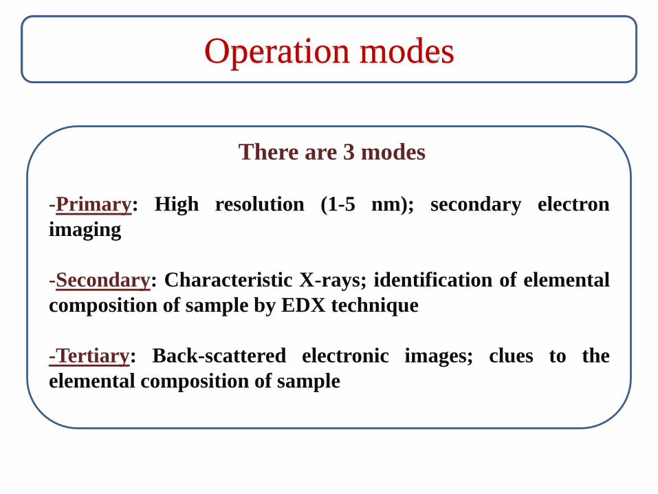
There are 3 modes
-Primary: High resolution (1-5 nm); secondary electron
imaging
-Secondary: Characteristic X-rays; identification of elemental
composition of sample by EDX technique
-Tertiary: Back-scattered electronic images; clues to the
elemental composition of sample
Operation modes
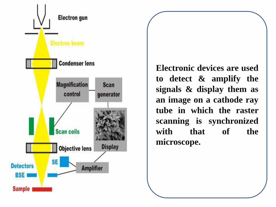
Electronic devices are used
to detect & amplify the
signals & display them as
an image on a cathode ray
tube in which the raster
scanning is synchronized
with that of the
microscope.
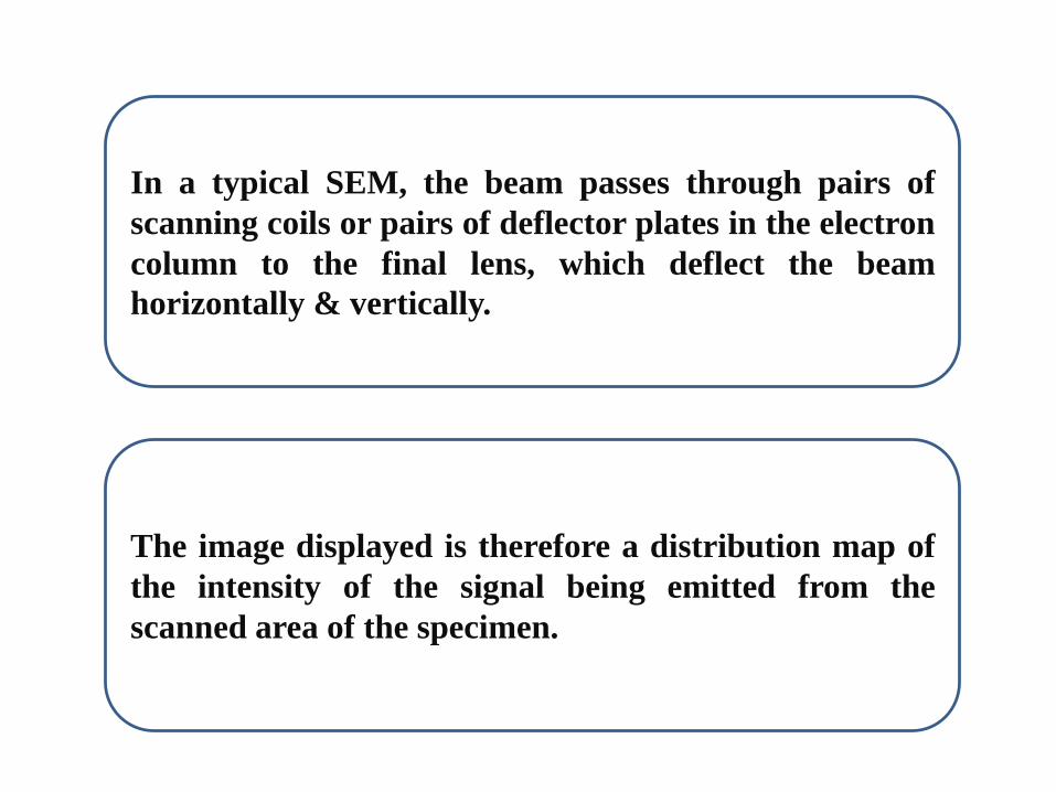
In a typical SEM, the beam passes through pairs of
scanning coils or pairs of deflector plates in the electron
column to the final lens, which deflect the beam
horizontally & vertically.
The image displayed is therefore a distribution map of
the intensity of the signal being emitted from the
scanned area of the specimen.
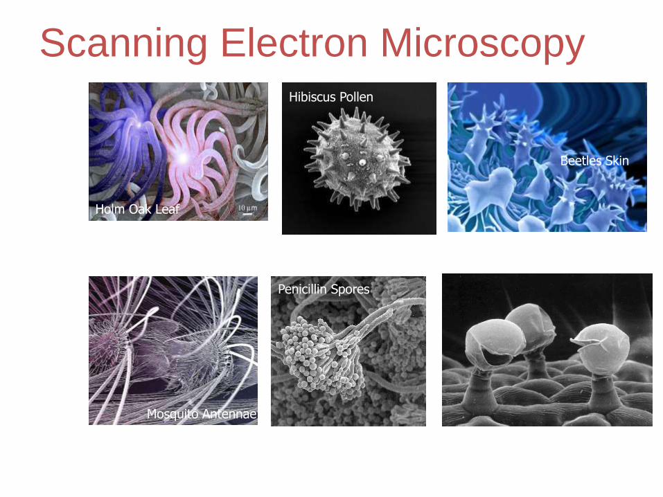
Scanning Electron Microscopy
Mosquito Antennae
Holm Oak Leaf
Penicillin Spores
Hibiscus Pollen
Beetles Skin
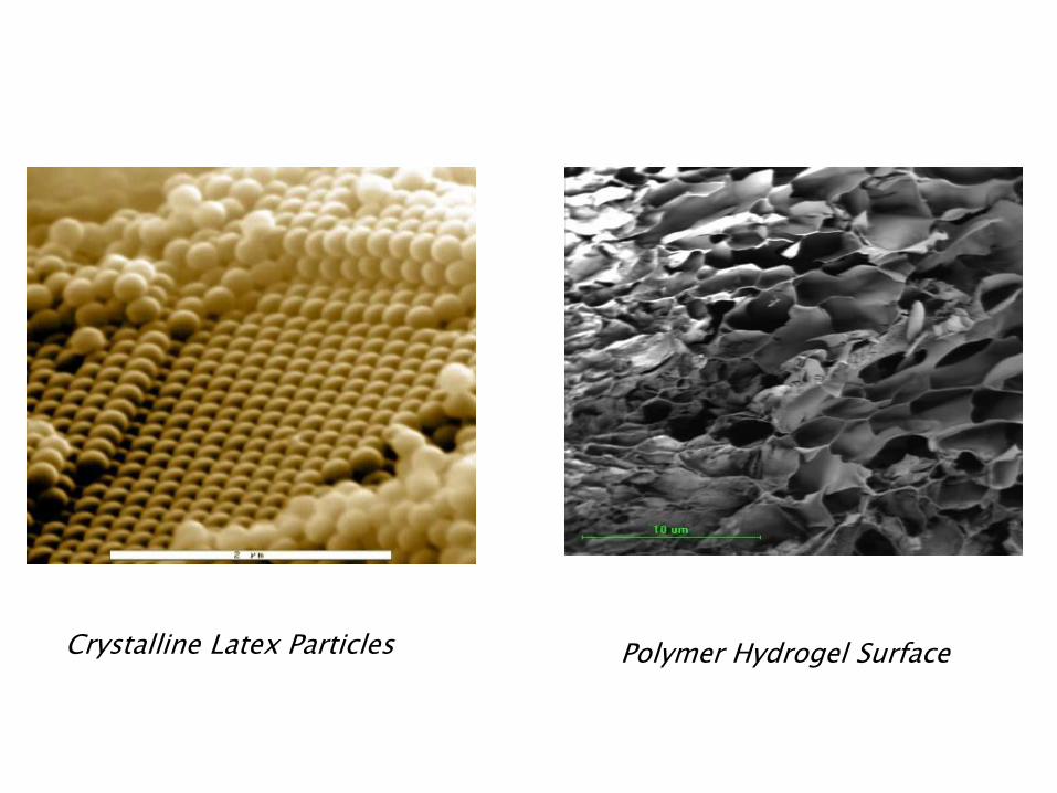
Crystalline Latex Particles Polymer Hydrogel Surface
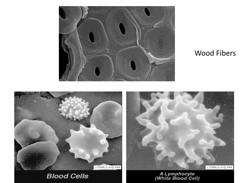
Wood Fibers
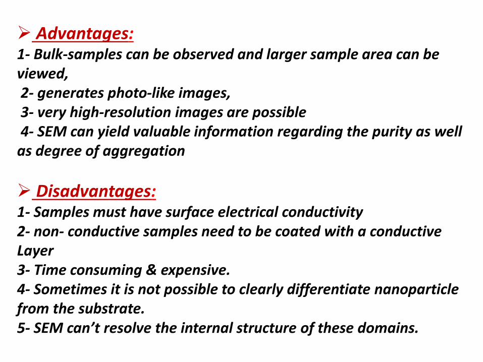
Advantages: 1- Bulk-samples can be observed and larger sample area can be viewed,2- generates photo-like images,3- very high-resolution images are possible4- SEM can yield valuable information regarding the purity as well as degree of aggregation
Disadvantages: 1- Samples must have surface electrical conductivity2- non- conductive samples need to be coated with a conductive Layer 3- Time consuming & expensive.4- Sometimes it is not possible to clearly differentiate nanoparticlefrom the substrate.5- SEM can’t resolve the internal structure of these domains.
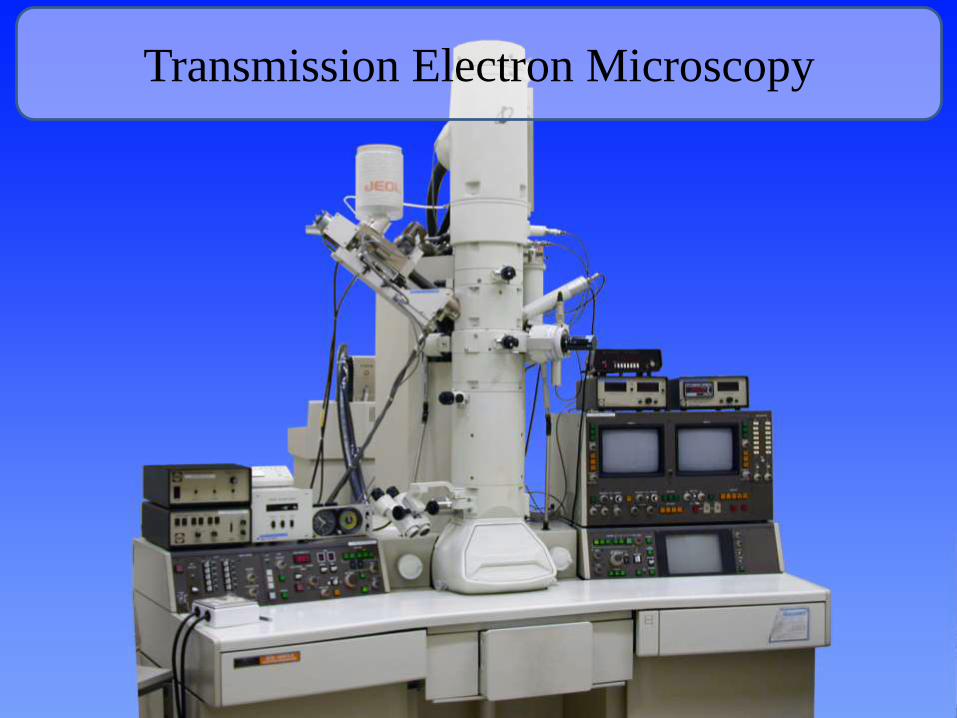
Transmission Electron Microscopy
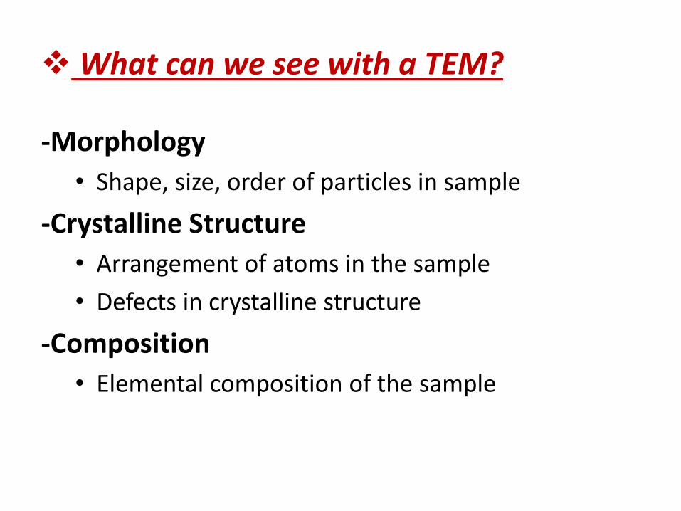
-Morphology
• Shape, size, order of particles in sample
-Crystalline Structure
• Arrangement of atoms in the sample
• Defects in crystalline structure
-Composition
• Elemental composition of the sample
What can we see with a TEM?
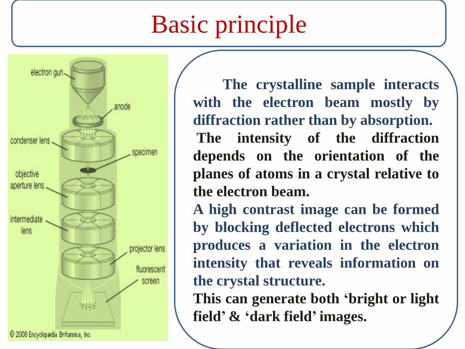
The crystalline sample interacts
with the electron beam mostly by
diffraction rather than by absorption.
The intensity of the diffraction
depends on the orientation of the
planes of atoms in a crystal relative to
the electron beam.
A high contrast image can be formed
by blocking deflected electrons which
produces a variation in the electron
intensity that reveals information on
the crystal structure.
This can generate both ‘bright or light
field’& ‘dark field’ images.
Basic principle
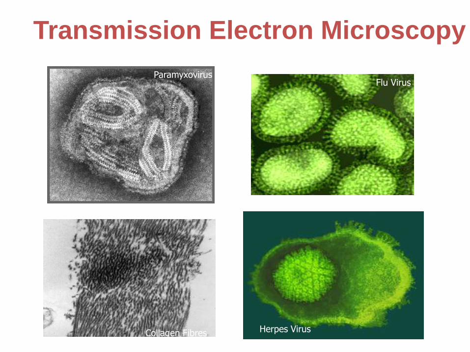
Transmission Electron Microscopy
Collagen Fibres Herpes Virus
Paramyxovirus Flu Virus
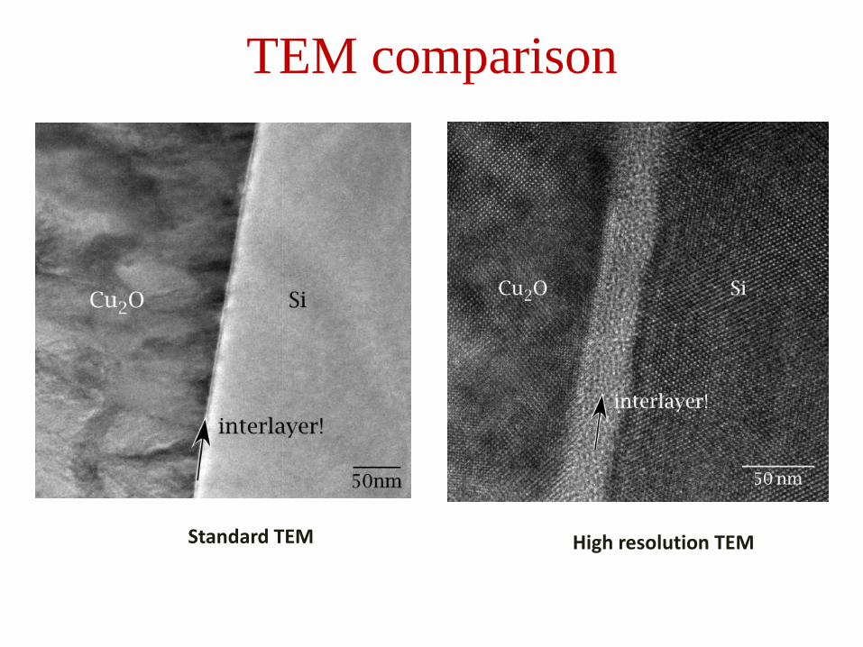
TEM comparison
Standard TEM High resolution TEMStandard TEM High resolution TEM
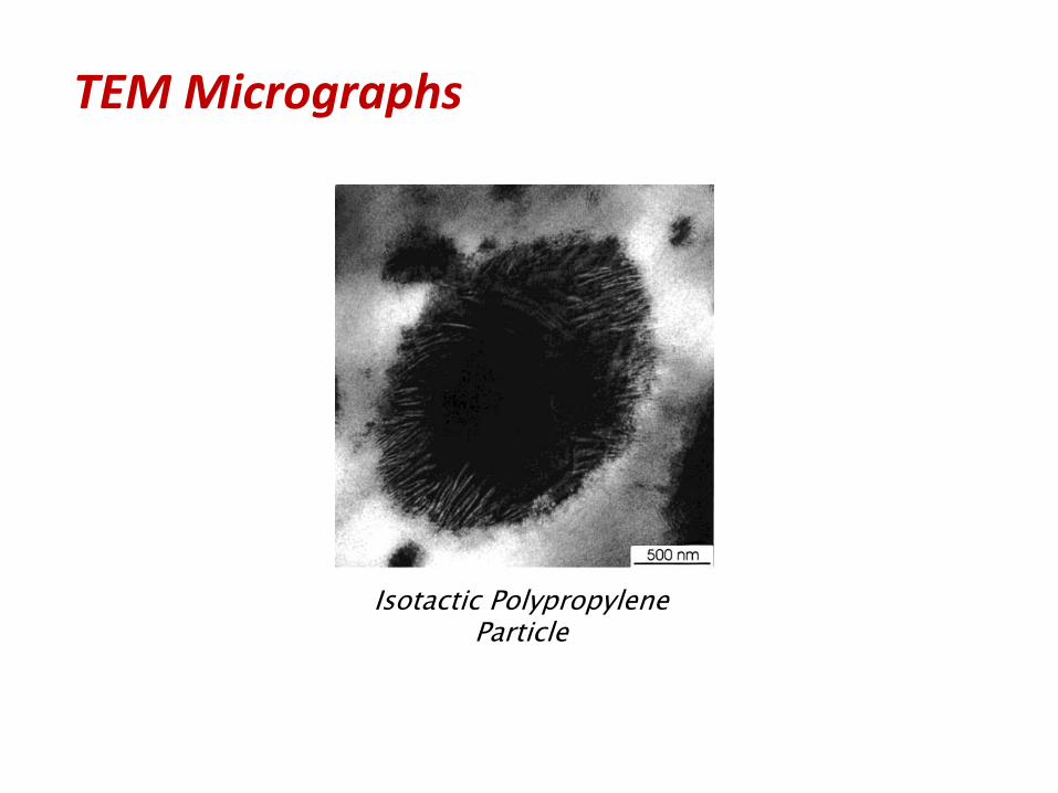
Isotactic Polypropylene Particle
TEM Micrographs
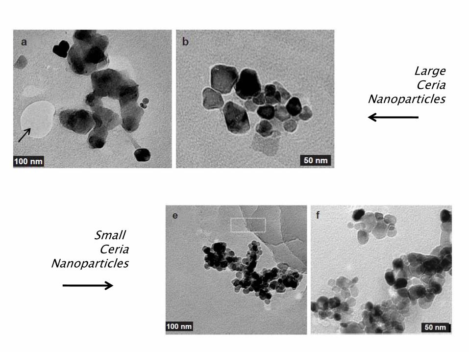
LargeCeria
Nanoparticles
Small Ceria
Nanoparticles
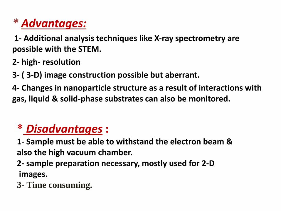
* Advantages:1- Additional analysis techniques like X-ray spectrometry are
possible with the STEM.
2- high- resolution
3- ( 3-D) image construction possible but aberrant.
4- Changes in nanoparticle structure as a result of interactions with gas, liquid & solid-phase substrates can also be monitored.
* Disadvantages :1- Sample must be able to withstand the electron beam & also the high vacuum chamber.2- sample preparation necessary, mostly used for 2-D images.3- Time consuming.
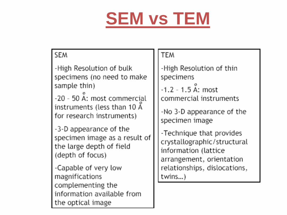
SEM vs TEM
Synthesis and optical characterization of copper oxide nanoparticles:
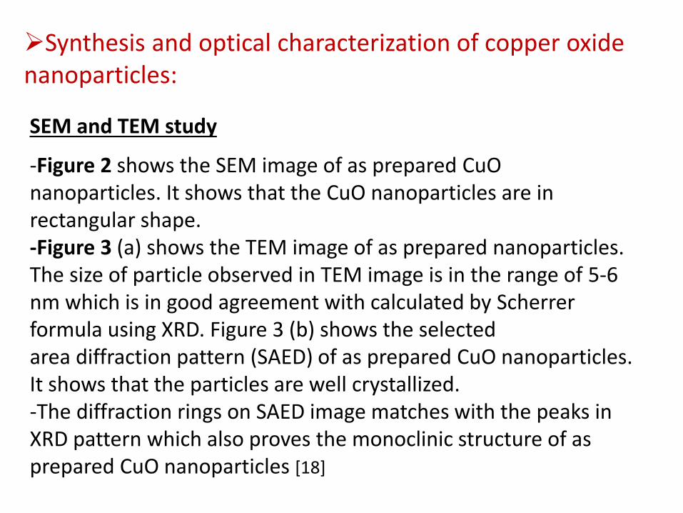
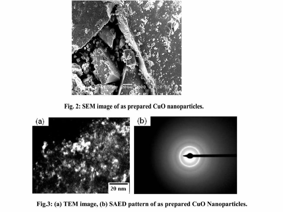
SEM and TEM study
-Figure 2 shows the SEM image of as prepared CuOnanoparticles. It shows that the CuO nanoparticles are in rectangular shape.-Figure 3 (a) shows the TEM image of as prepared nanoparticles. The size of particle observed in TEM image is in the range of 5-6 nm which is in good agreement with calculated by Scherrerformula using XRD. Figure 3 (b) shows the selected area diffraction pattern (SAED) of as prepared CuO nanoparticles. It shows that the particles are well crystallized. -The diffraction rings on SAED image matches with the peaks in XRD pattern which also proves the monoclinic structure of as prepared CuO nanoparticles [18]
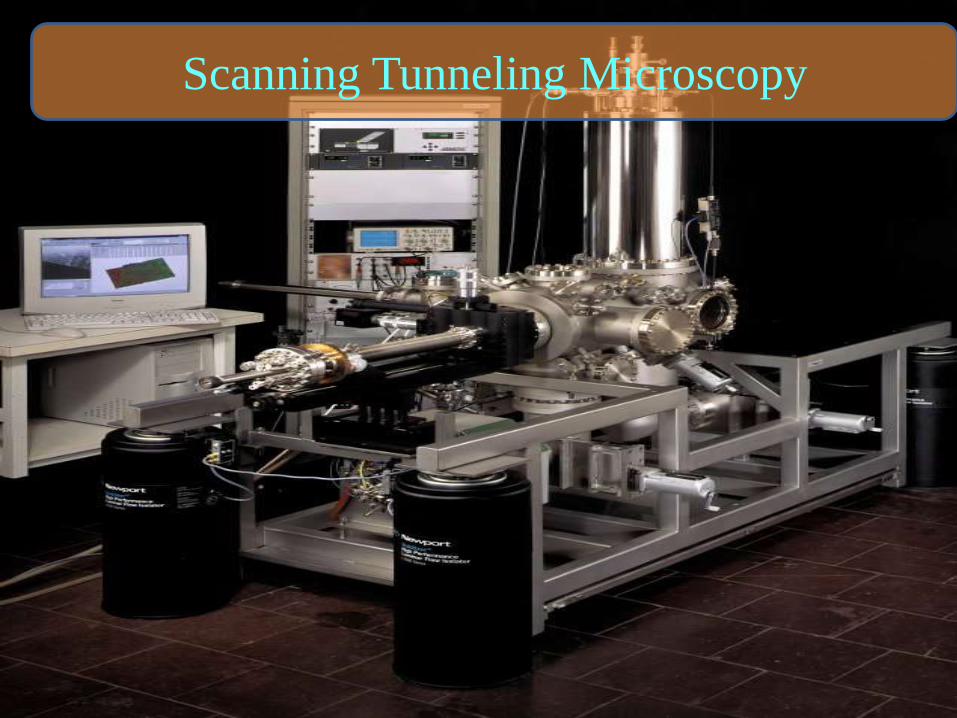
Scanning Tunneling Microscopy
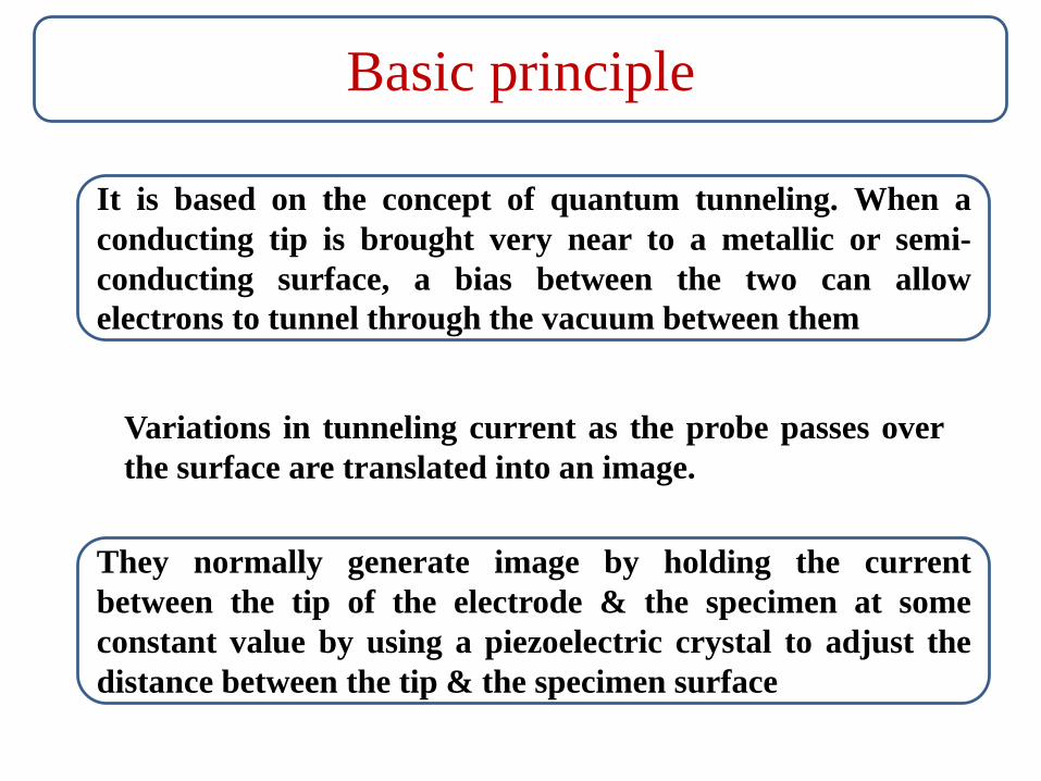
Basic principle
It is based on the concept of quantum tunneling. When a
conducting tip is brought very near to a metallic or semi-
conducting surface, a bias between the two can allow
electrons to tunnel through the vacuum between them.
Variations in tunneling current as the probe passes over
the surface are translated into an image.
They normally generate image by holding the current
between the tip of the electrode & the specimen at some
constant value by using a piezoelectric crystal to adjust the
distance between the tip & the specimen surface.
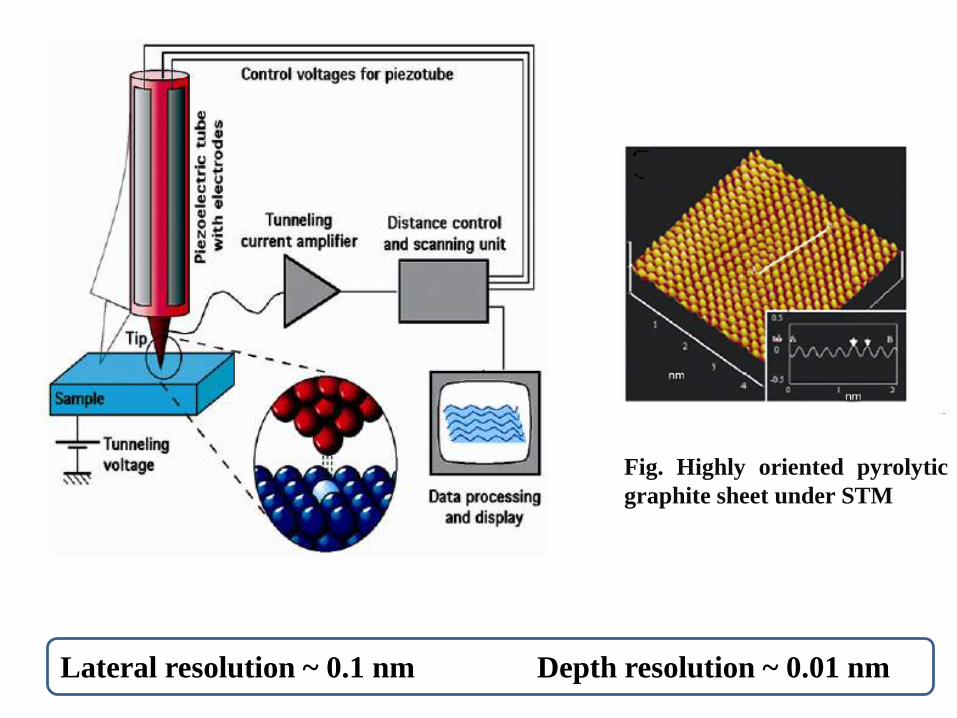
Lateral resolution ~ 0.1 nm Depth resolution ~ 0.01 nm
Fig. Highly oriented pyrolytic
graphite sheet under STM
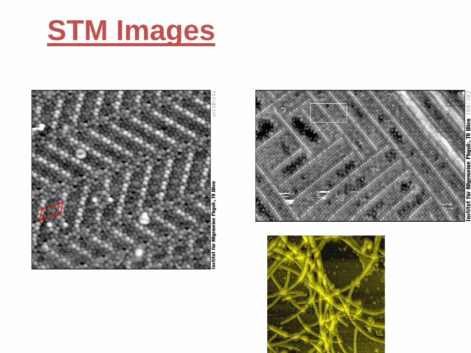
STM Images
Advantages: 1- Very high image resolution (capable of „seeing‟ and manipulating atoms).
2- STM can be used not only in ultra high vacuum but also in air & various other liquid or gas, at ambient & wide range of temperature.
Disadvantages :1- Again
2- radius of curvature of tip3- extremely sensitive to ambient vibrations4- STM can be a challenging technique, as it requires extremely clean surfaces & sharp tips.
Spectroscopy
1- X-ray Diffraction (XRD) 2- Small Angle X-ray Scattering (SAXS)3- X-ray Photoelectron Spectroscopy ( XPS )4- UV-vis spectroscopy 5- FT-IR spectroscopy
Optical Spectroscopy
Optical spectroscopy uses the interaction of light with matter as a function of wavelength or energy in order to obtain information about the material.
Typical penetration depth is of the order of 50 nm. Optical spectroscopy is attractive for materials characterization because it is fast, nondestructive and of high resolution.
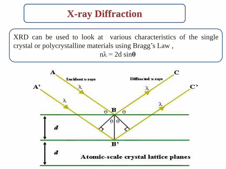
X-ray Diffraction
XRD can be used to look at various characteristics of the single
crystal or polycrystalline materials using Bragg’s Law ,
nλ = 2d sinθ
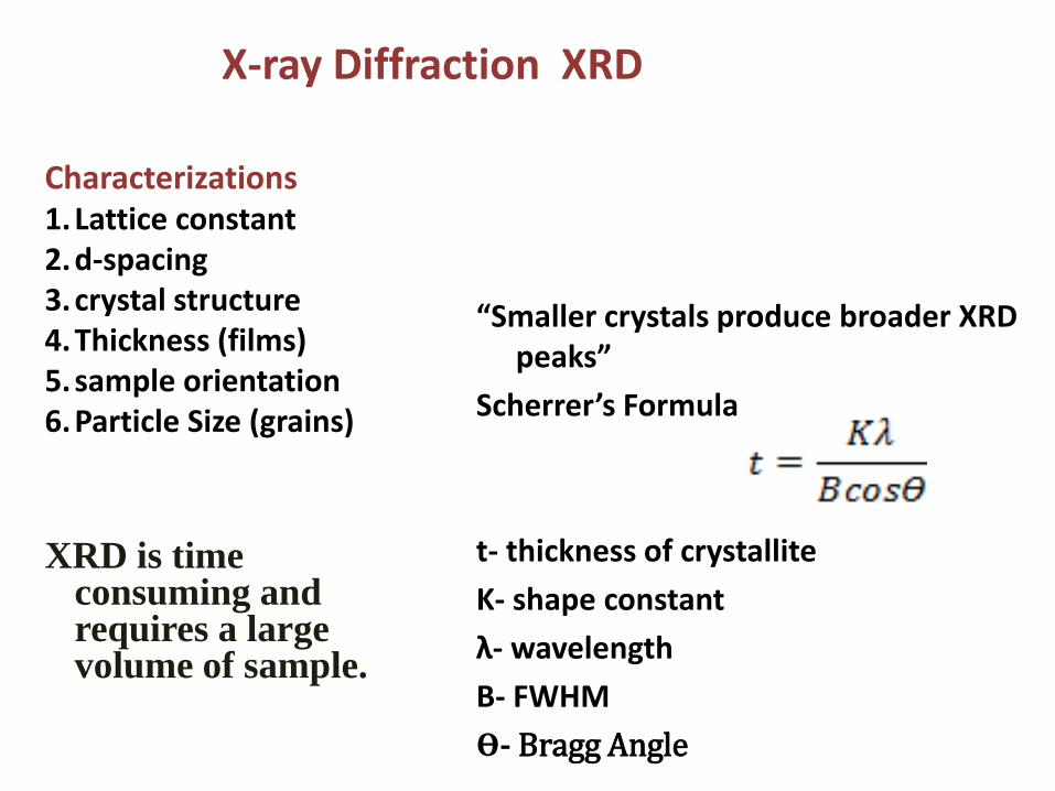
X-ray Diffraction XRD
“Smaller crystals produce broader XRD peaks”
Scherrer’s Formula
t- thickness of crystallite
K- shape constant
λ- wavelength
B- FWHM
ϴ- Bragg Angle
Characterizations1.Lattice constant2.d-spacing3.crystal structure4.Thickness (films)5.sample orientation6.Particle Size (grains)
XRD is time consuming and requires a large volume of sample.
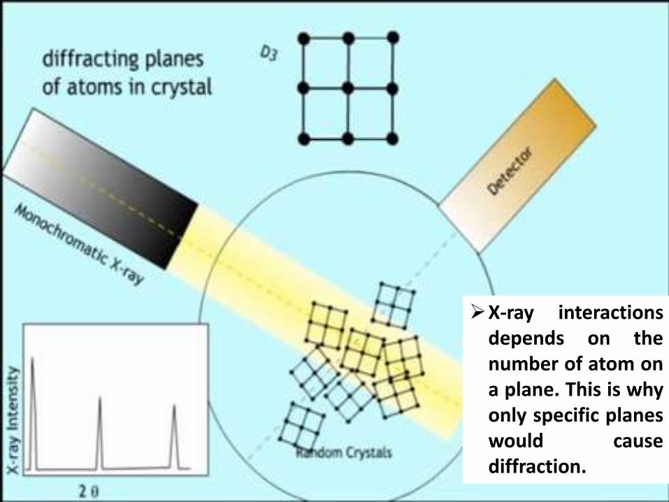
X-ray interactionsdepends on thenumber of atom ona plane. This is whyonly specific planeswould causediffraction.
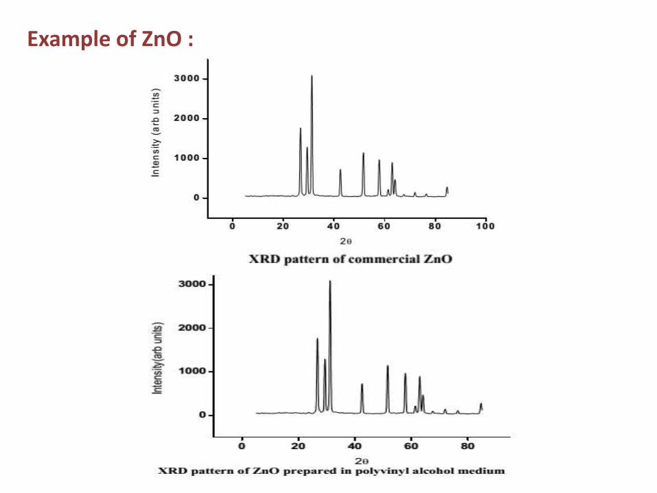
Example of ZnO :
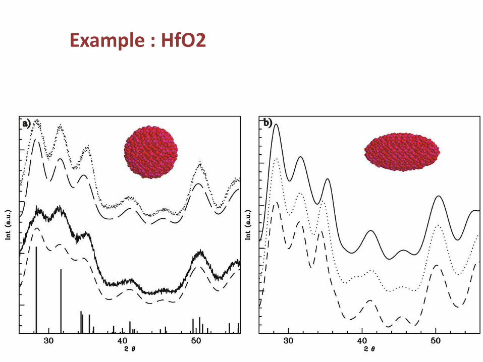
Example : HfO2
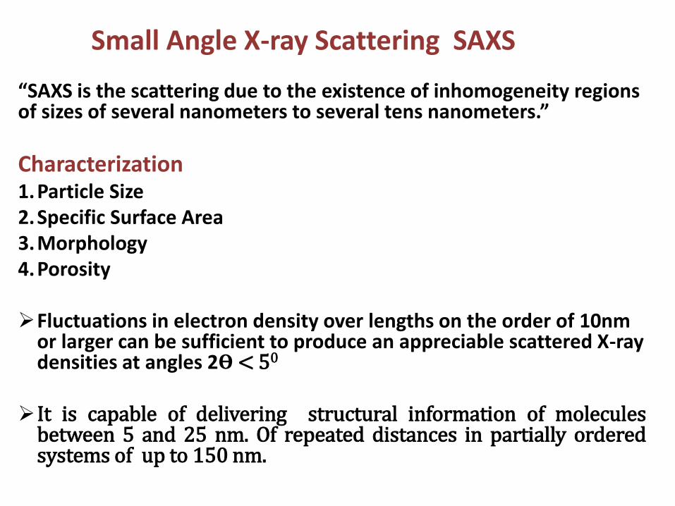
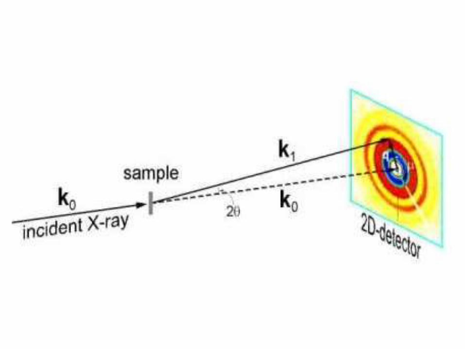
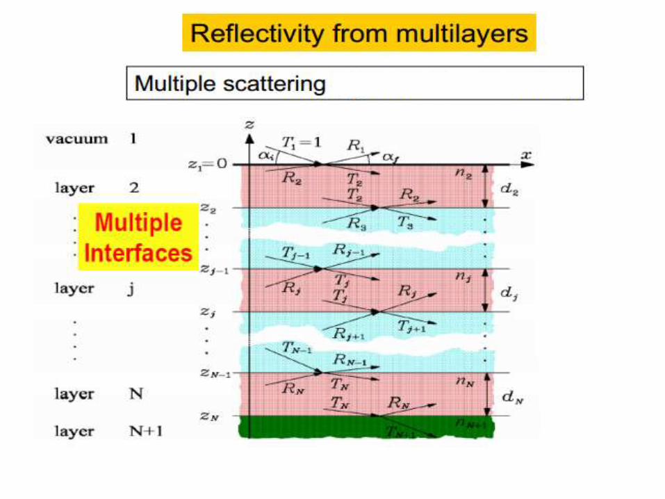
Small Angle X-ray Scattering SAXS
“SAXS is the scattering due to the existence of inhomogeneity regions of sizes of several nanometers to several tens nanometers.”
Characterization1.Particle Size2.Specific Surface Area3.Morphology4.Porosity
Fluctuations in electron density over lengths on the order of 10nm or larger can be sufficient to produce an appreciable scattered X-ray densities at angles 2ϴ< 50
It is capable of delivering structural information of moleculesbetween 5 and 25 nm. Of repeated distances in partially orderedsystems of up to 150 nm.
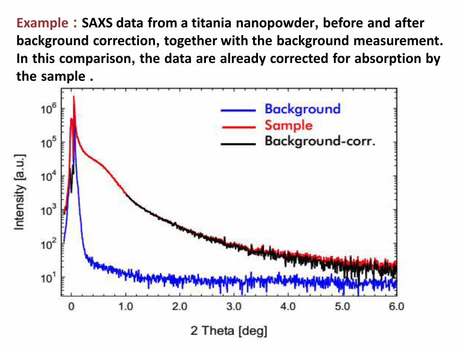
Example : SAXS data from a titania nanopowder, before and afterbackground correction, together with the background measurement. In this comparison, the data are already corrected for absorption bythe sample .
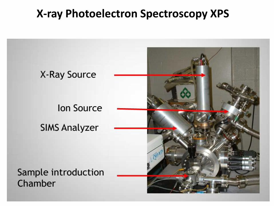
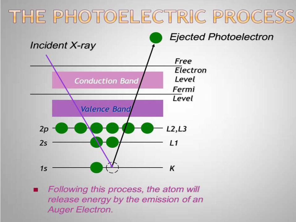
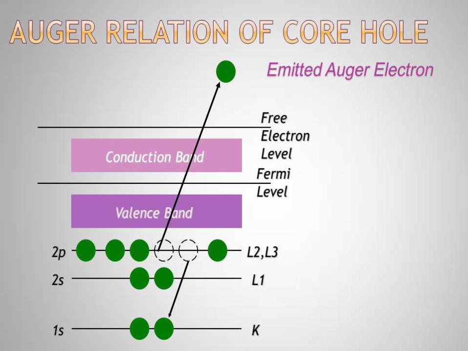
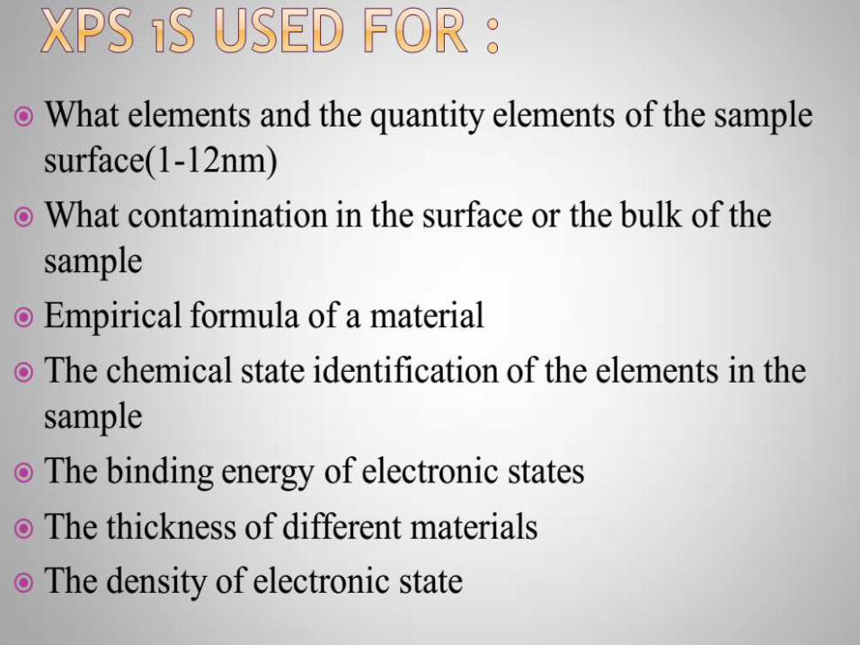
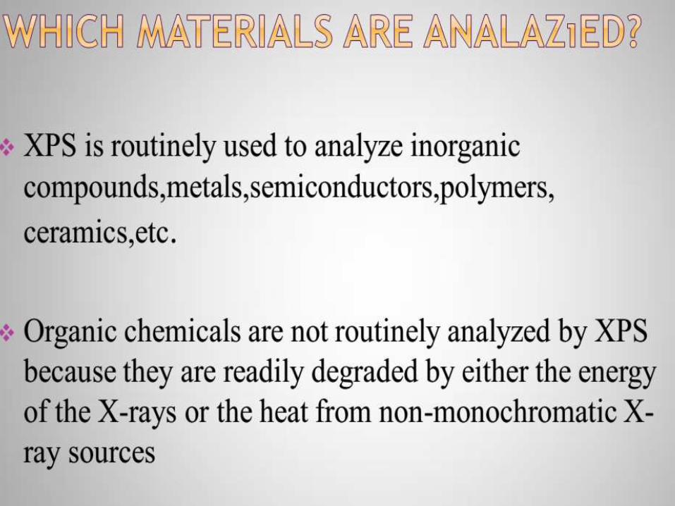
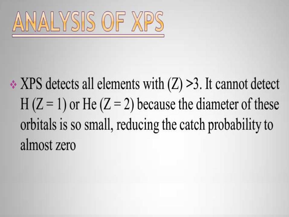
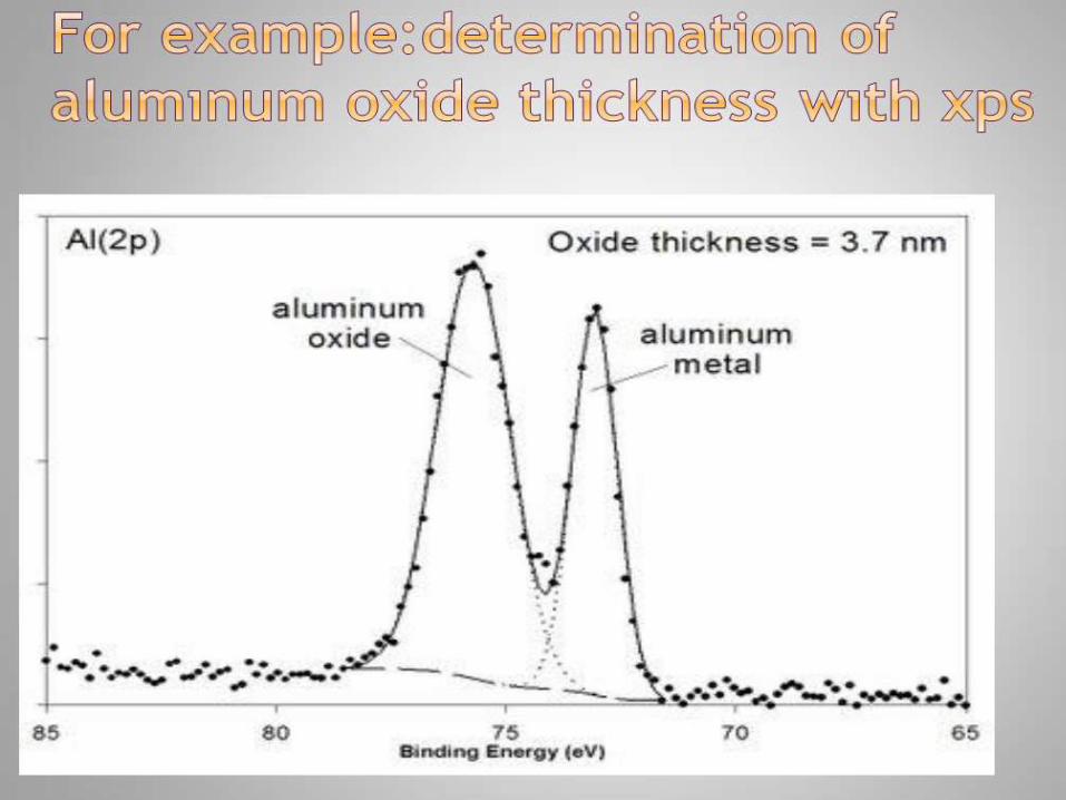
X-ray Photoelectron Spectroscopy XPS
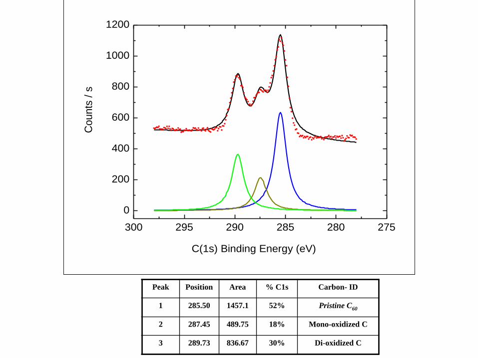
300 295 290 285 280 275
0
200
400
600
800
1000
1200
Co
unts
/ s
C(1s) Binding Energy (eV)
Peak Position Area % C1s Carbon- ID
1 285.50 1457.1 52% Pristine C60
2 287.45 489.75 18% Mono-oxidized C
3 289.73 836.67 30% Di-oxidized C
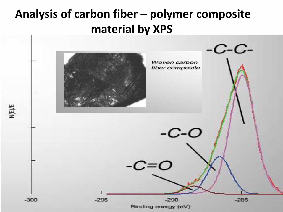
Analysis of carbon fiber – polymer compositematerial by XPS
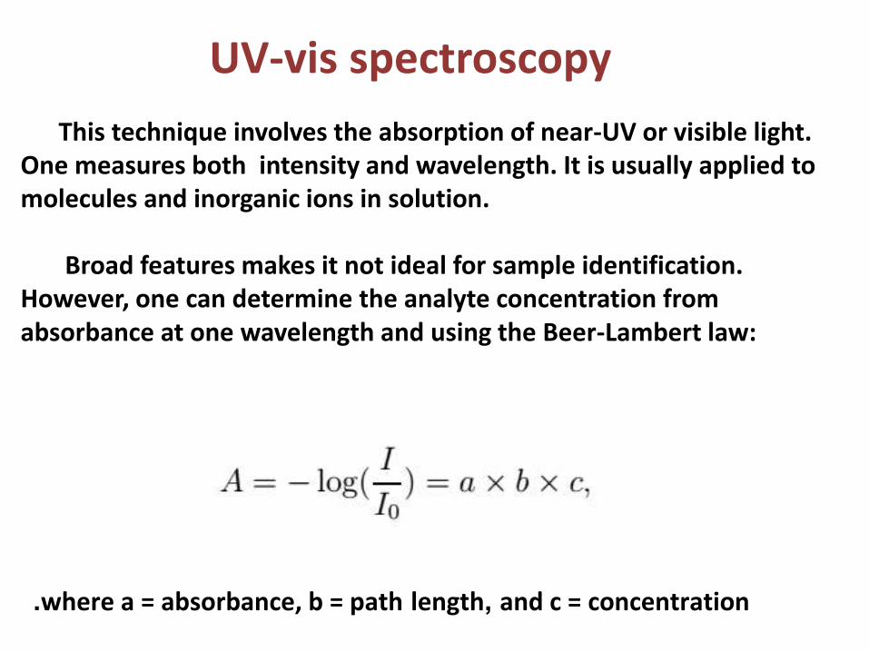
This technique involves the absorption of near-UV or visible light. One measures both intensity and wavelength. It is usually applied to molecules and inorganic ions in solution.
Broad features makes it not ideal for sample identification. However, one can determine the analyte concentration from absorbance at one wavelength and using the Beer-Lambert law:
where a = absorbance, b = path length, and c = concentration .
UV-vis spectroscopy
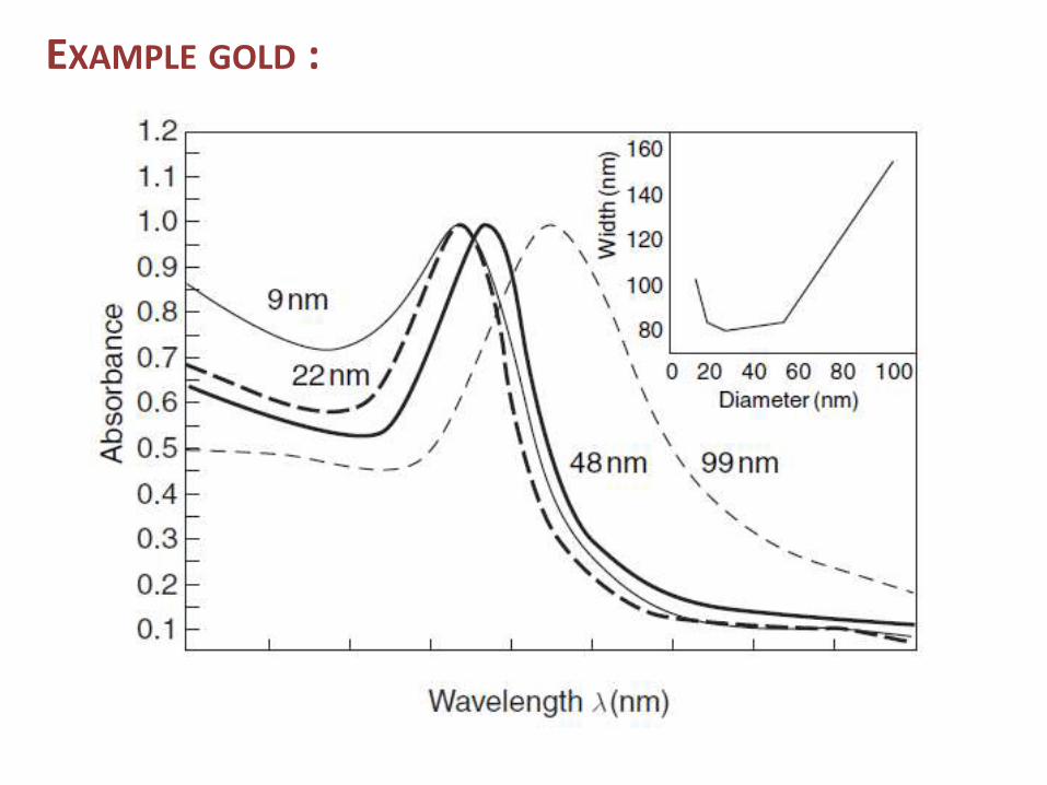
EXAMPLE GOLD :
52
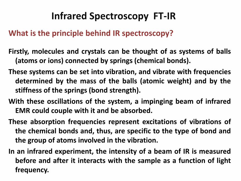
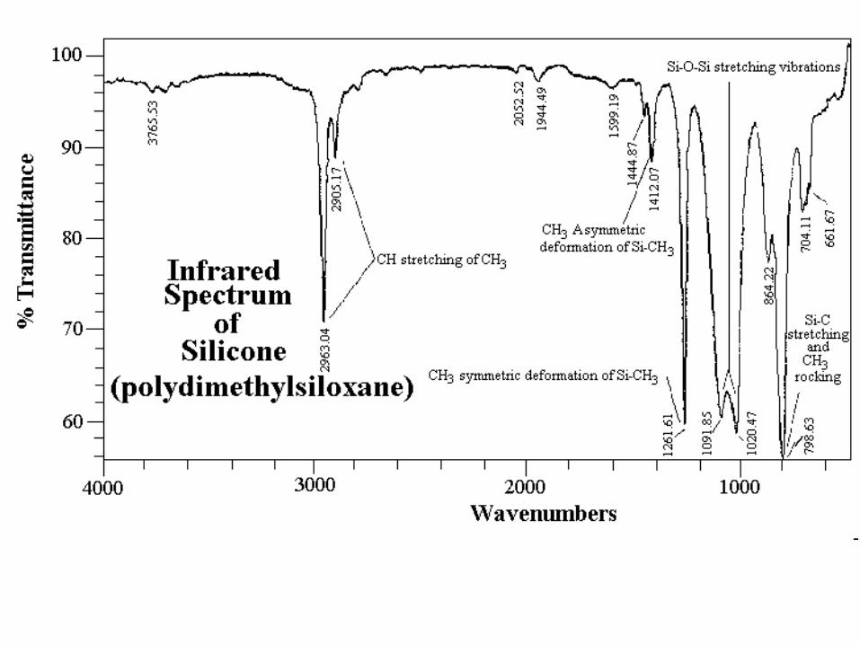
Infrared Spectroscopy FT-IR
What is the principle behind IR spectroscopy?
Firstly, molecules and crystals can be thought of as systems of balls(atoms or ions) connected by springs (chemical bonds).
These systems can be set into vibration, and vibrate with frequenciesdetermined by the mass of the balls (atomic weight) and by thestiffness of the springs (bond strength).
With these oscillations of the system, a impinging beam of infraredEMR could couple with it and be absorbed.
These absorption frequencies represent excitations of vibrations ofthe chemical bonds and, thus, are specific to the type of bond andthe group of atoms involved in the vibration.
In an infrared experiment, the intensity of a beam of IR is measuredbefore and after it interacts with the sample as a function of lightfrequency.
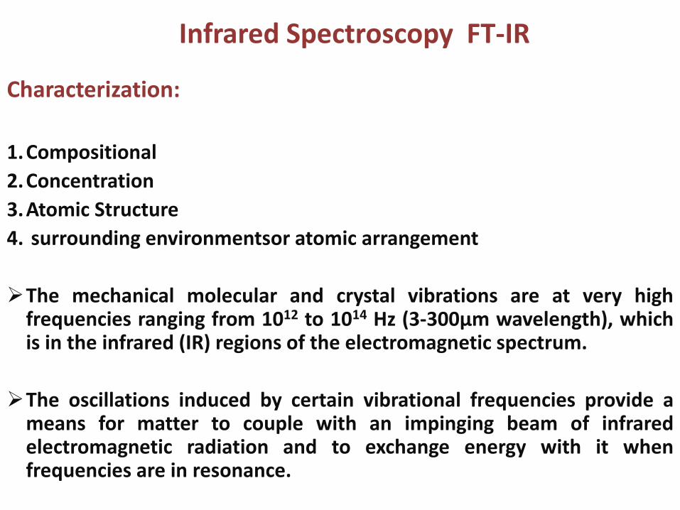
Characterization:
1.Compositional
2.Concentration
3.Atomic Structure
4. surrounding environmentsor atomic arrangement
The mechanical molecular and crystal vibrations are at very highfrequencies ranging from 1012 to 1014 Hz (3-300μm wavelength), whichis in the infrared (IR) regions of the electromagnetic spectrum.
The oscillations induced by certain vibrational frequencies provide ameans for matter to couple with an impinging beam of infraredelectromagnetic radiation and to exchange energy with it whenfrequencies are in resonance.
Infrared Spectroscopy FT-IR