Embed Size (px)
Citation preview
InAs Nanowires
substrate preparation &
growth dynamics
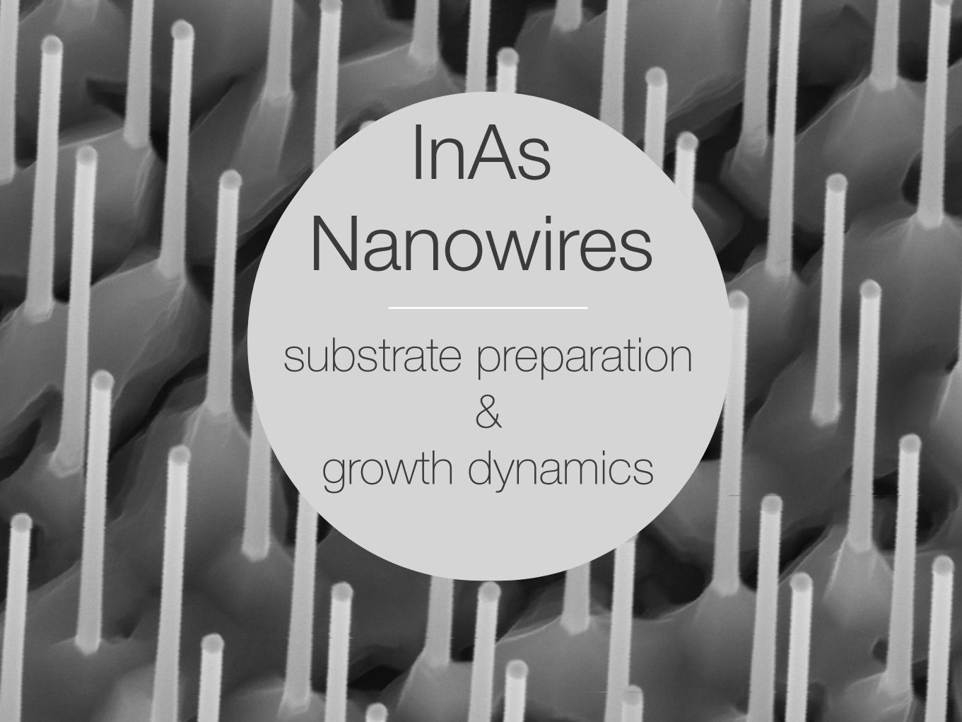
nano-fabrication
structural - characterisations
thermodynamics & kinetics
ME+
coffee+
sleep deprivationnanowire
growth growthkinetics
Outline
• Introduction
• Substrates
• Growth Dynamics*
3
* in progress
Nanowires
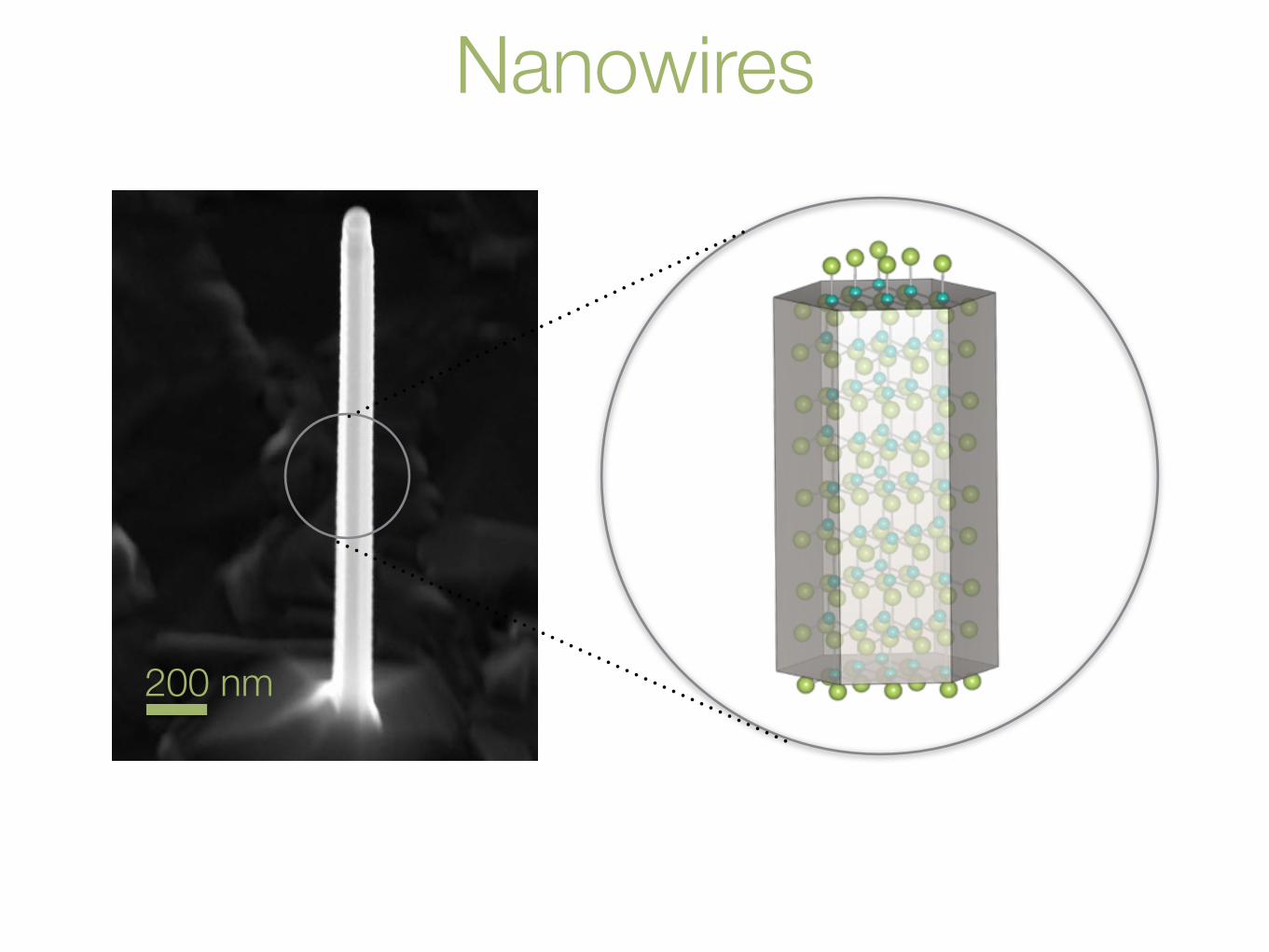
Nanowires
200 nm
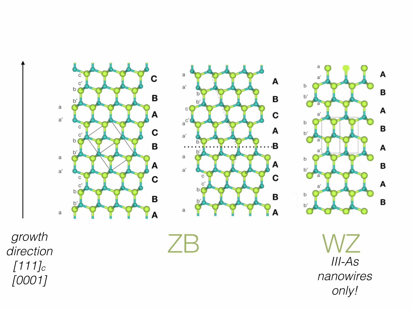
WZZBIII-As
nanowires only!
growth direction
[111]c [0001]
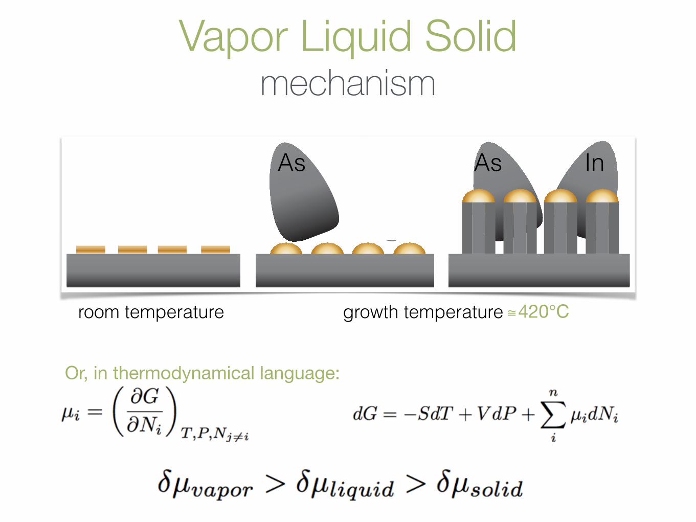
Vapor Liquid Solidmechanism
As As In
room temperature growth temperature≅420℃
Or, in thermodynamical language:
molecular beam epitaxy (MBE)
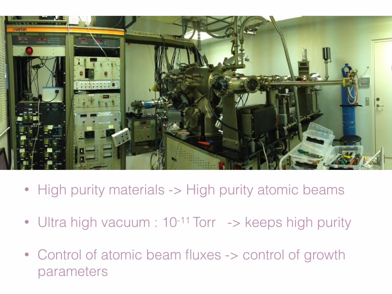
• High purity materials -> High purity atomic beams
• Ultra high vacuum : 10-11 Torr -> keeps high purity
• Control of atomic beam fluxes -> control of growth parameters
Substrates
• Fabrication process overview
• Position control & size control
• Substrates for NW network
• Novel InAs -SiO2
10
20 μm
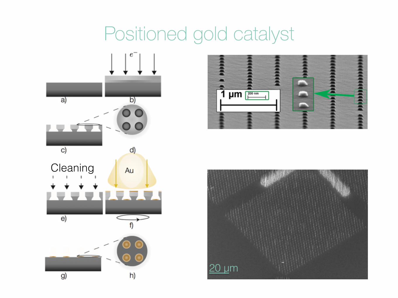
Positioned gold catalyst
Cleaning
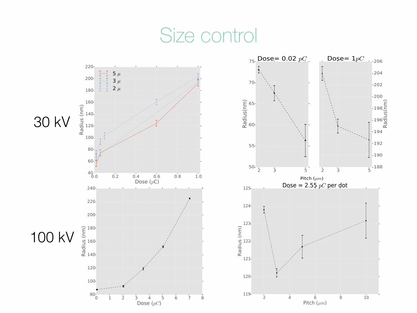
Size control
30 kV
100 kV
• Catalyst volume -> NW diameter & growth rate • NW diameter -> NW properties! • Catalyst position -> creation of NW networks
why care about volume and position control ?
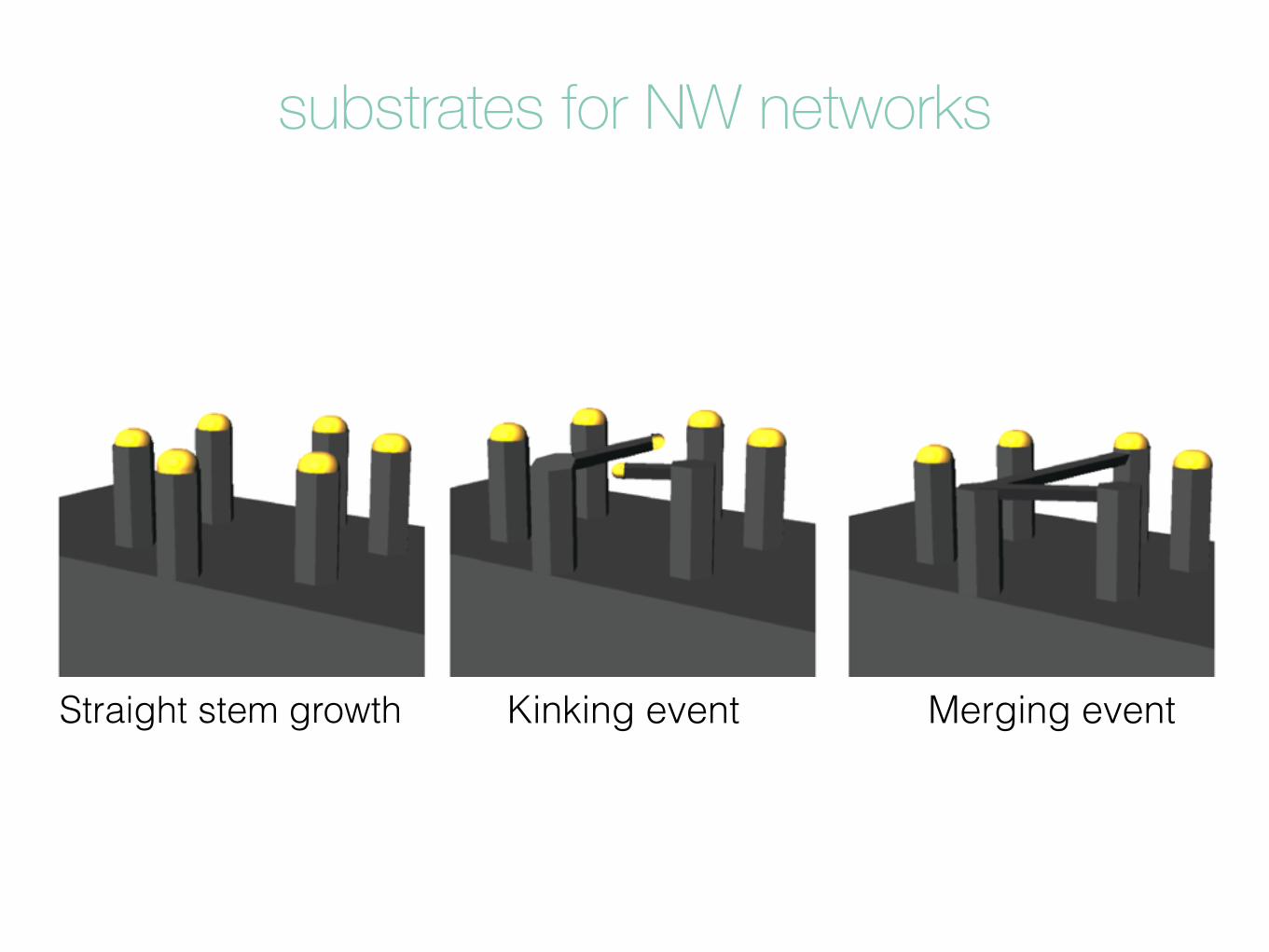
Kinking eventStraight stem growth Merging event
substrates for NW networks
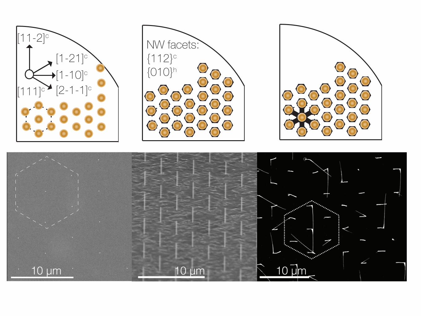
[11-2]c
[1-10]c[1-21]c
[2-1-1]c
NW facets:{112}c
{010}h
[111]c
10 μm 10 μm 10 μm
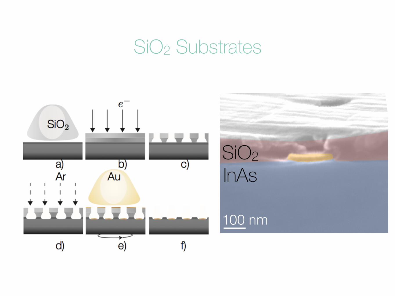
SiO2 Substrates
• Novel SiO2 and InAs
100 nm
SiO2InAs
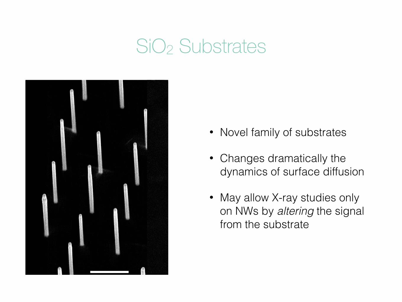
• Novel family of substrates
• Changes dramatically the dynamics of surface diffusion
• May allow X-ray studies only on NWs by altering the signal from the substrate
SiO2 Substrates
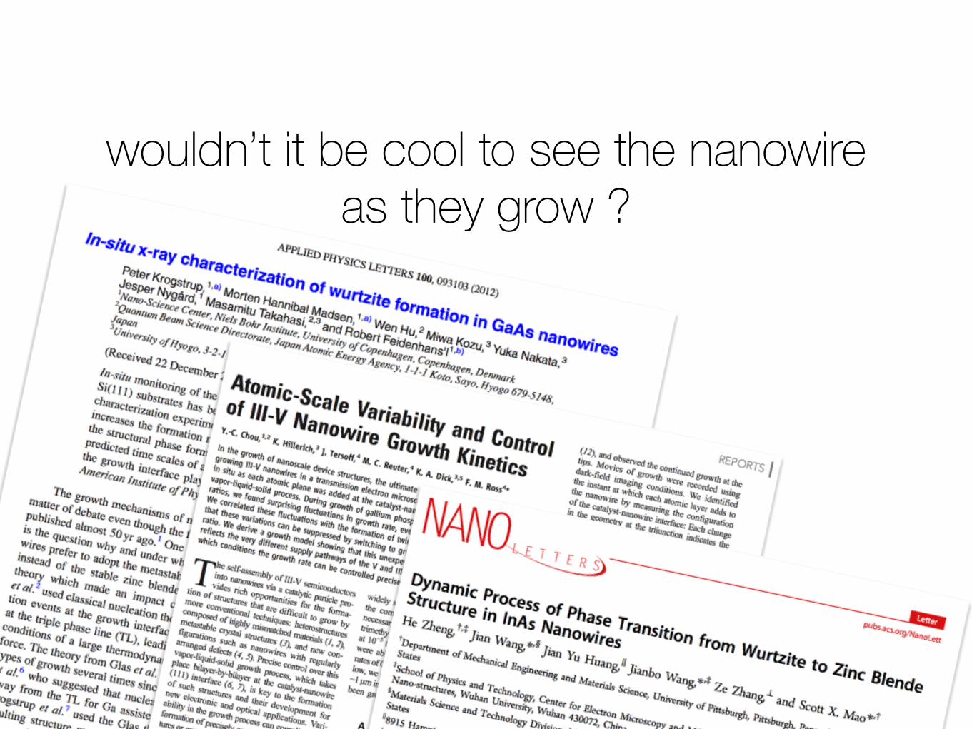
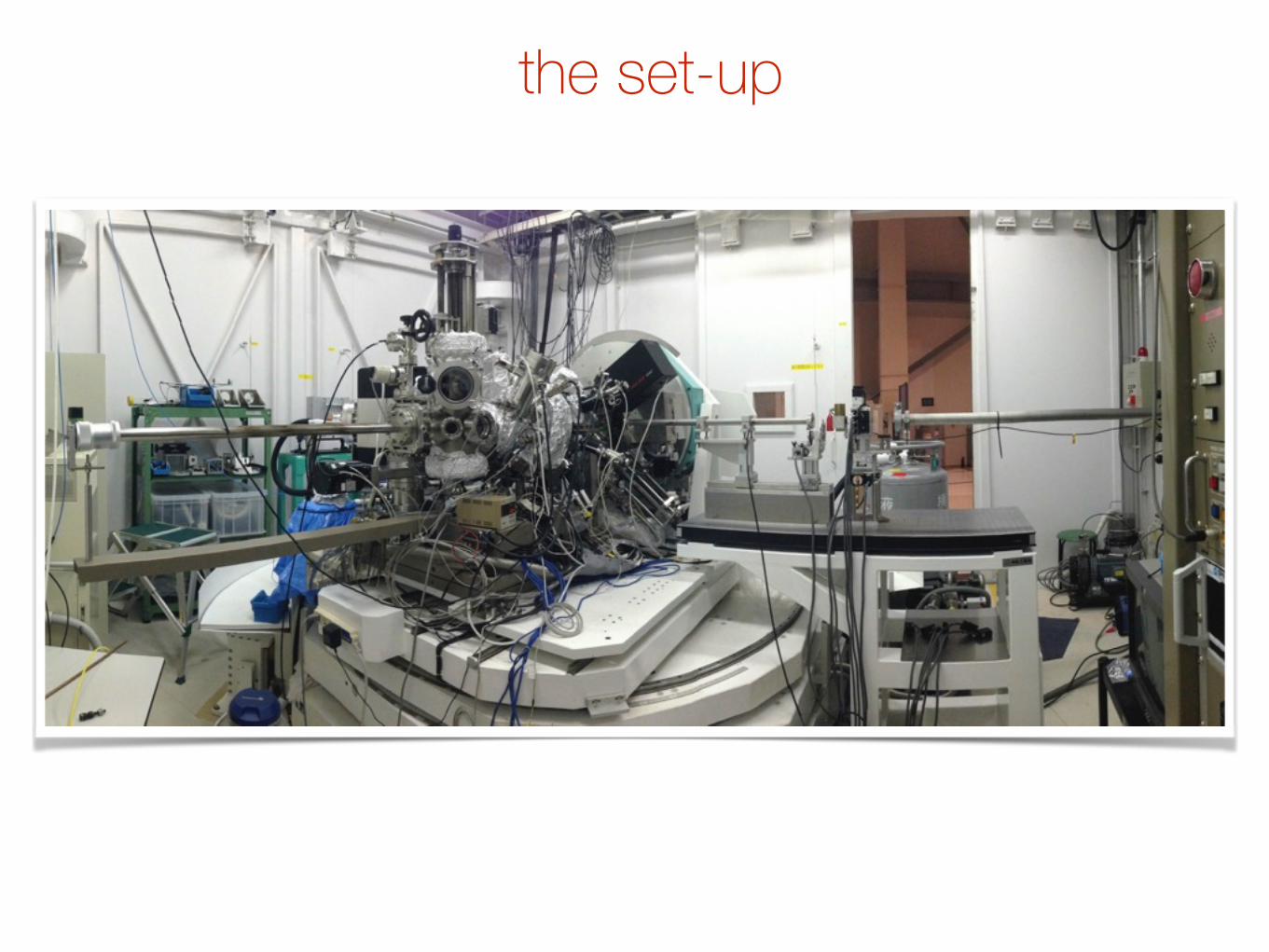
wouldn’t it be cool to see the nanowire as they grow ?
in-stu X-ray diffraction
BL11XU @
SPring8
*Preliminary results
the set-up
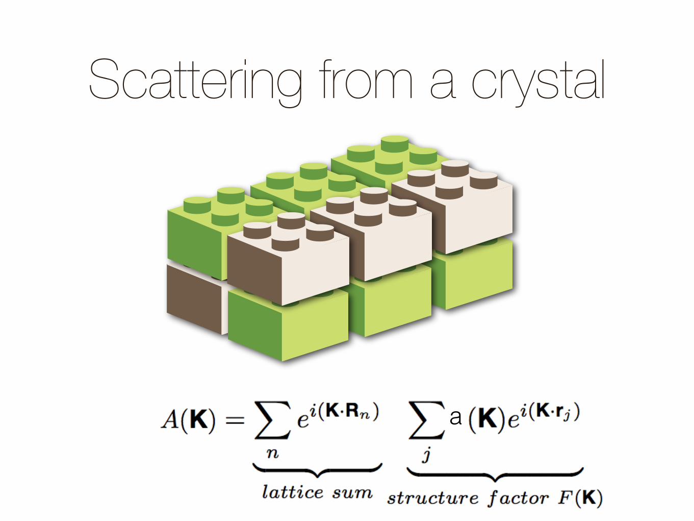
Scattering from a crystal
a
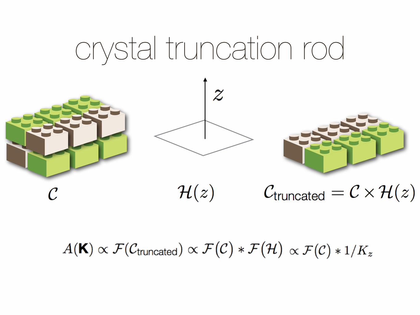
crystal truncation rod
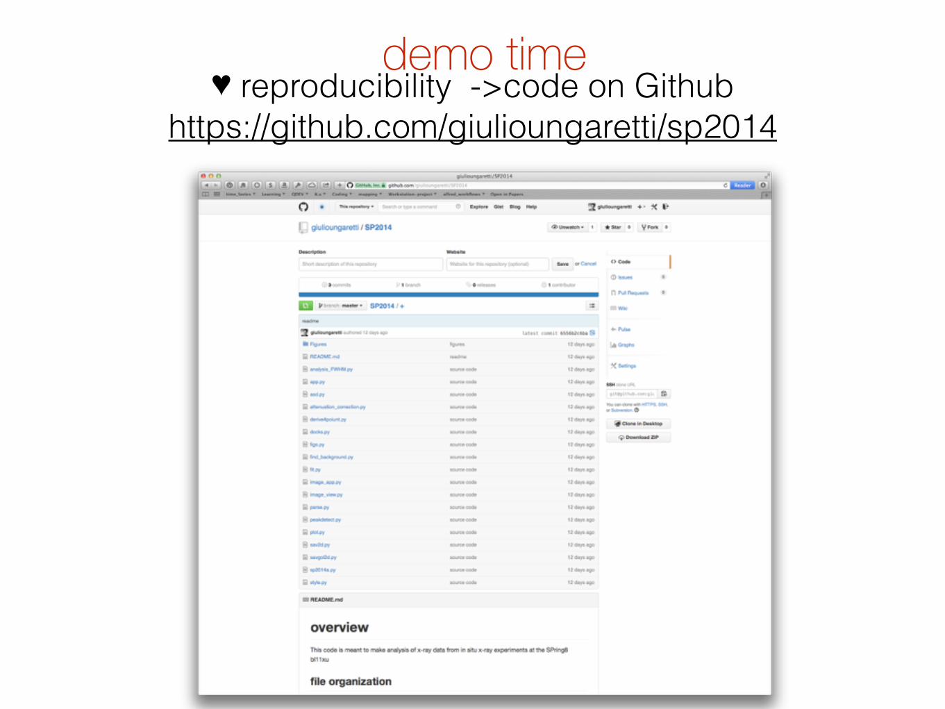
demo time♥ reproducibility ->code on Github
https://github.com/giulioungaretti/sp2014
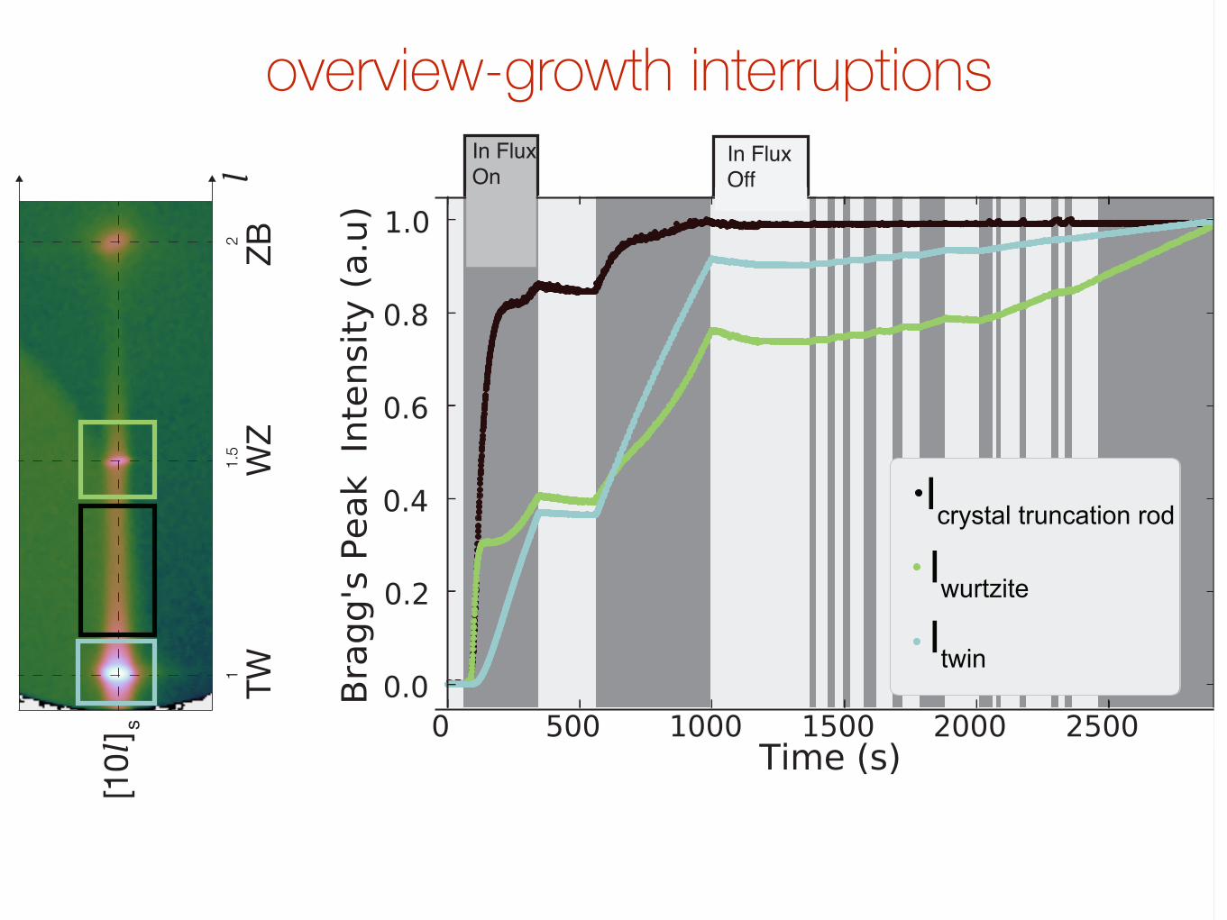
Icrystal truncation rod
Iwurtzite
Itwin
In Flux
On
In Flux
Off
[10l
] s
11.5
2l
TWWZ
ZB
overview-growth interruptions
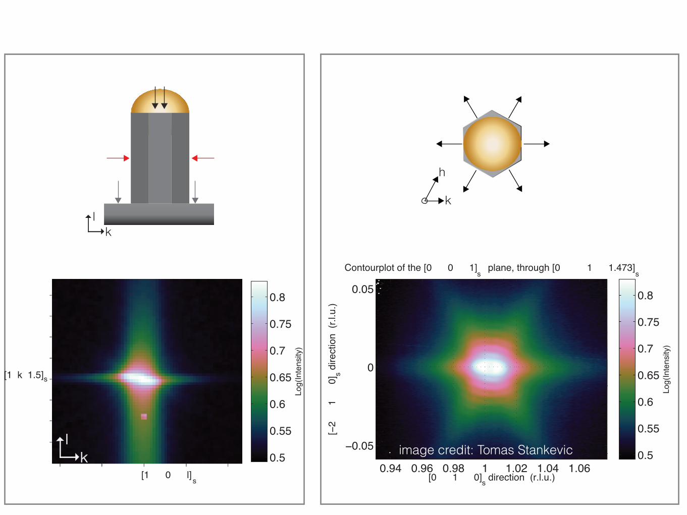
[0 1 0]s direction (r.l.u.)
[−2
1
0]s d
irect
ion
(r.l.
u.)
Contourplot of the [0 0 1] plane, through [0 1 1.473]
0.94 0.96 0.98 1 1.02 1.04 1.06
−0.05
0
0.05
Log(
Inte
nsity
)
0.5
0.55
0.6
0.65
0.7
0.75
0.8
s s
[1 0 l]s
Log(
Inte
nsity
)
0.5
0.55
0.6
0.65
0.7
0.75
0.8
[1 k 1.5]s
lk
lk
k
h
image credit: Tomas Stankevic
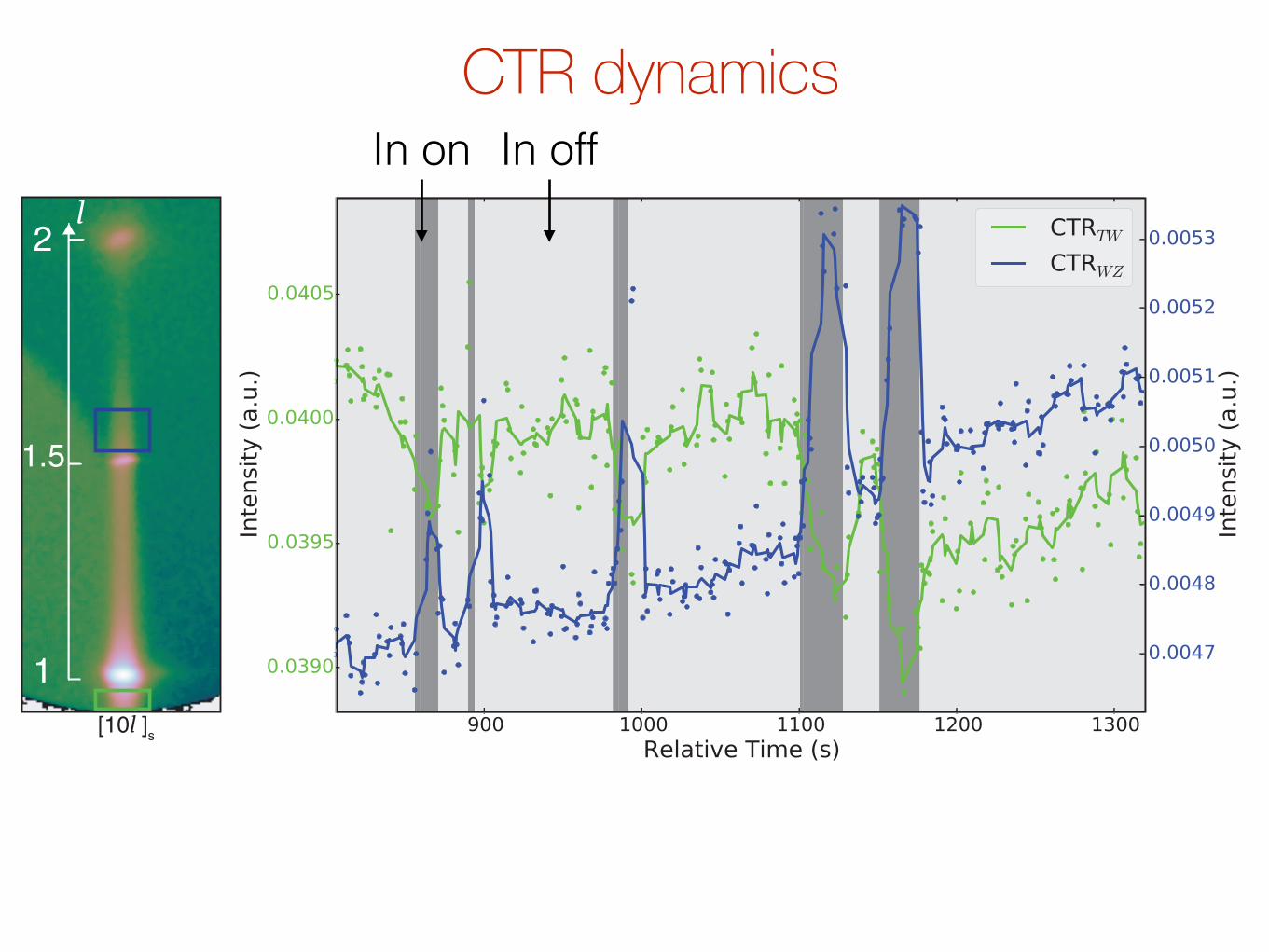
2
1.5
1
l
[10l ]s
CTR dynamicsIn on In off
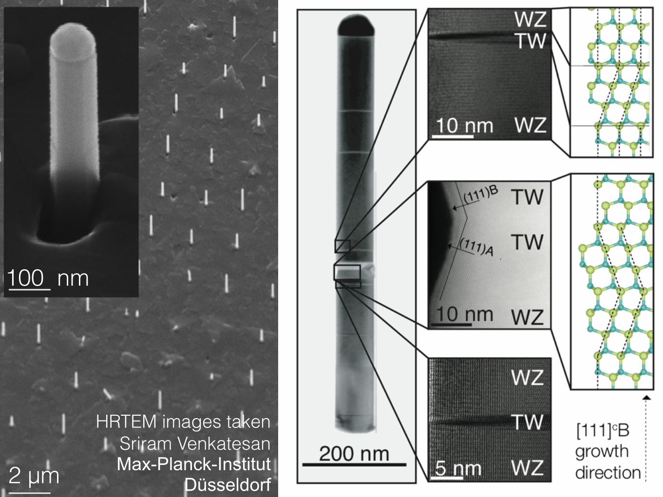
HRTEM images taken Sriram Venkatesan Max-Planck-Institut
Düsseldorf
100 nm
2 μm
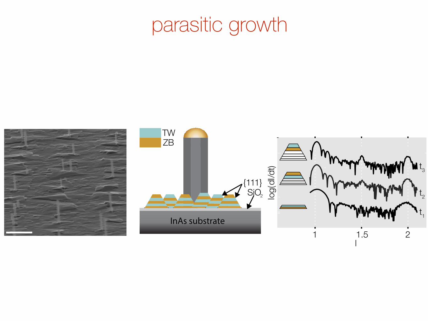
ZB
TW
1 1.5 2
l
log(dI/dt)
{111}
SiO2
InAs substratet1
t2
t3
parasitic growth
Conclusion and acknowledgements • Substrates can be fabricated with high control over
both size and position
• Promising results in fabrication on NW network
• Insights on growth dynamics
♥Jesper and Peter ♥all QDever’s and in particular yesterday’s night crew ♥DNRF-DANSCATT - Japan Trips funding ♥DNRF & Microsoft station Q - General lab funding and espresso