Embed Size (px)
Citation preview
2009/07/17 copy right by Dr. Len Mei 2017 1
Dr. Len Mei
Discussion on Advanced
Semiconductor
Photolithographic
Technologies
Moore’s Law and
Photolithography
Moore’s Law is mostly enabled by photolithographic
technology
To print smaller feature size, light of smaller
wavelength is needed to minimize light interference
and diffraction.
2 2009/07/17
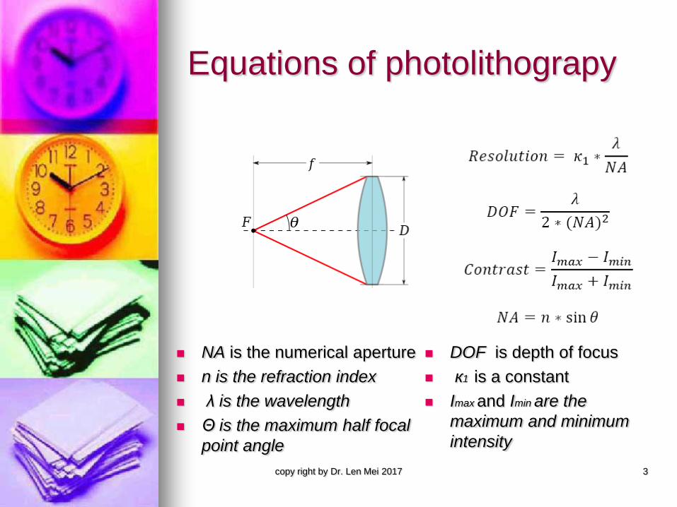
Equations of photolithograpy
copy right by Dr. Len Mei 2017 3
NA is the numerical aperture
n is the refraction index
λ is the wavelength
Θ is the maximum half focal
point angle
DOF is depth of focus
к1 is a constant
Imax and Imin are the
maximum and minimum
intensity
Wavelength vs. technology
copy right by Dr. Len Mei 200907 4 2009/07/17
ArF 193 nm
4:1 KrF 248 nm
5:1 G-line 436 nm
5:1 I-line 365 nm
Vis
ible
light
Deep U
V
EUV 13.5 nm E
UV
1:1 G-line 436 nm
157 nm EUV was abondaned.
Technology development at
user side (wafer fab)
copy right by Dr. Len Mei 2017 5
Other photolithographic technologies to
compensate longer wavelength
All other techniques to enhance resolution
are generally known as Resolution
Enhancement Technique (RET)
RET above 60 nm
Optical proximity correction (OPC)
Off axis illumination (OAI)
Phase shift mask (PSM)
Hard mask (HM)
6 2009/07/17
Photolithographic technologies to
compensate longer wavelength
Below 60 nm, additional technologies are
required:
Double patterning (DP)
Multiple patterning (MP)
Restricted design rules (RDR)
Gridded design rules (GDR)
Source mask optimization (SMO)
Inverse lithography technology (ILT)
Negative tone development (NTD)
7 2009/07/17
Optical Proximity Correction
OPC is an enhancement technique to
compensate for image errors due
to diffraction or process effects.
OPC technique is to correct the shape of
pattern on the mask by moving edges or
adding extra polygons to the pattern, so
that the printed pattern will have the
desired shape.
8 2009/07/17
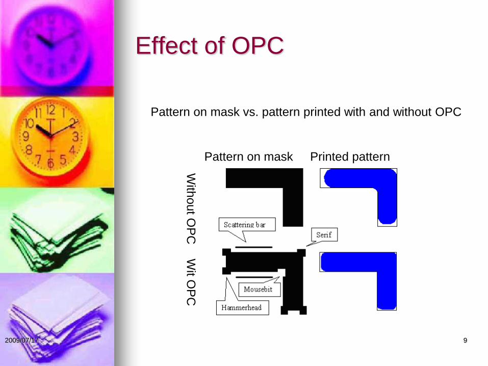
Effect of OPC
9 2009/07/17
Pattern on mask Printed pattern
With
out O
PC
W
it OP
C
Pattern on mask vs. pattern printed with and without OPC
Rule based and model based
OPC
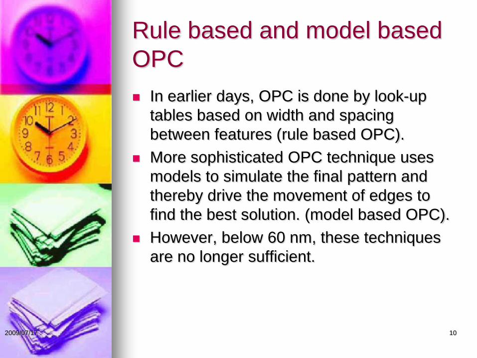
In earlier days, OPC is done by look-up
tables based on width and spacing
between features (rule based OPC).
More sophisticated OPC technique uses
models to simulate the final pattern and
thereby drive the movement of edges to
find the best solution. (model based OPC).
However, below 60 nm, these techniques
are no longer sufficient.
10 2009/07/17
Computational OPC
At smaller geometry, the pattern distortion may
depend on not only the pattern itself, but also the
environment the pattern is in.
For example, the pattern in densely populated area
may exhibit different pattern behavior than sparsely
populated area.
The computational OPC simulates the actual
lithographic process to obtain the final developed
polygons on wafer, then feedback the simulation
results to apply OPC on the mask.
With computational OPC, full chip lithography
simulation is possible.
11 2009/07/17
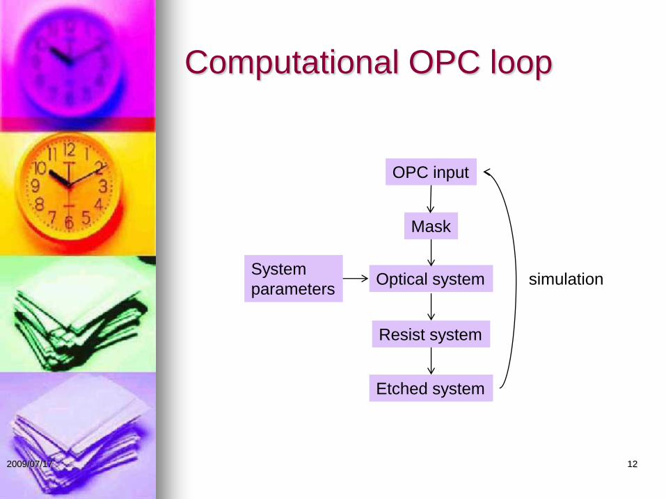
Computational OPC loop
12 2009/07/17
Optical system
Resist system
Mask
System
parameters
OPC input
Etched system
simulation
Source Mask Optimization
SMO is a new computational OPC. It is a full chip
mask synthesis solution.
It is to optimize mask patterns in conjunction with
illumination patterns by using algorithmic routines
and linear optimization capabilities to generate a
custom illumination source and a reticle.
It takes into account of the parameters of
lithography scanners needed to ensure
manufacturability.
SMO greatly extended the capability of immersion
scanner beyond 22 nm.
13 2009/07/17
Inverse Lithography
Technology
Inverse Lithography Technology is to design the
mask by starting from perfect pattern on wafer and
work backwards to incorporating all the system
introduced variations to be eliminated at the mask.
It requires extensive computation and full
characterization of the photolithographic process,
scanner, photoresist and mask.
copy right by Dr. Len Mei 2017 14
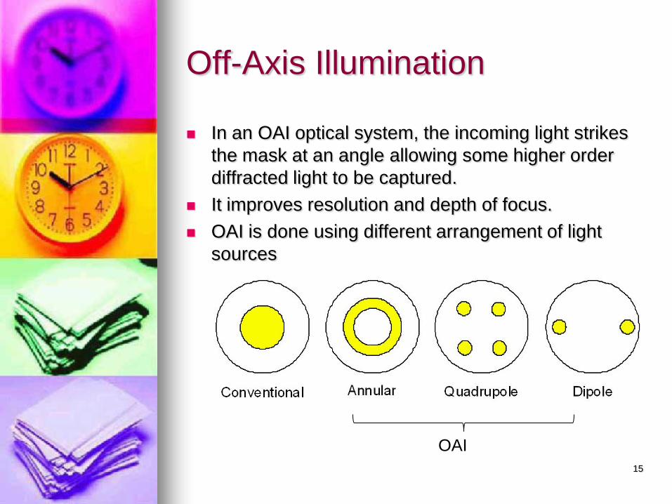
Off-Axis Illumination
In an OAI optical system, the incoming light strikes
the mask at an angle allowing some higher order
diffracted light to be captured.
It improves resolution and depth of focus.
OAI is done using different arrangement of light
sources
15
OAI
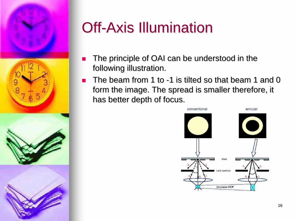
Off-Axis Illumination
The principle of OAI can be understood in the
following illustration.
The beam from 1 to -1 is tilted so that beam 1 and 0
form the image. The spread is smaller therefore, it
has better depth of focus.
16
Phase Shift Mask
PSM’s use the interference generated by light wave
phase differences through different mask thickness
to improve resolution.
There are two types of PSM:
Alternating
Attenuated
In alternating phase-shift masks, certain transmitting
regions are made thinner or thicker so that te light
traveling through adjacent paths shift phase by 180
degree, thus having the effect of improving
the contrast and the resolution. Plot of scattered
light (normalized to incident light) as a function of
the phase of a phase edge.
17
Phase Shift Mask
In an attenuated phase-shift masks, The light-
blocking parts of the mask are modified to allow a
small amount of light to be transmitted through. That
light is not strong enough to print a pattern on the
wafer, but it can interfere with the light coming from
the transparent parts of the mask.
18 2009/07/17
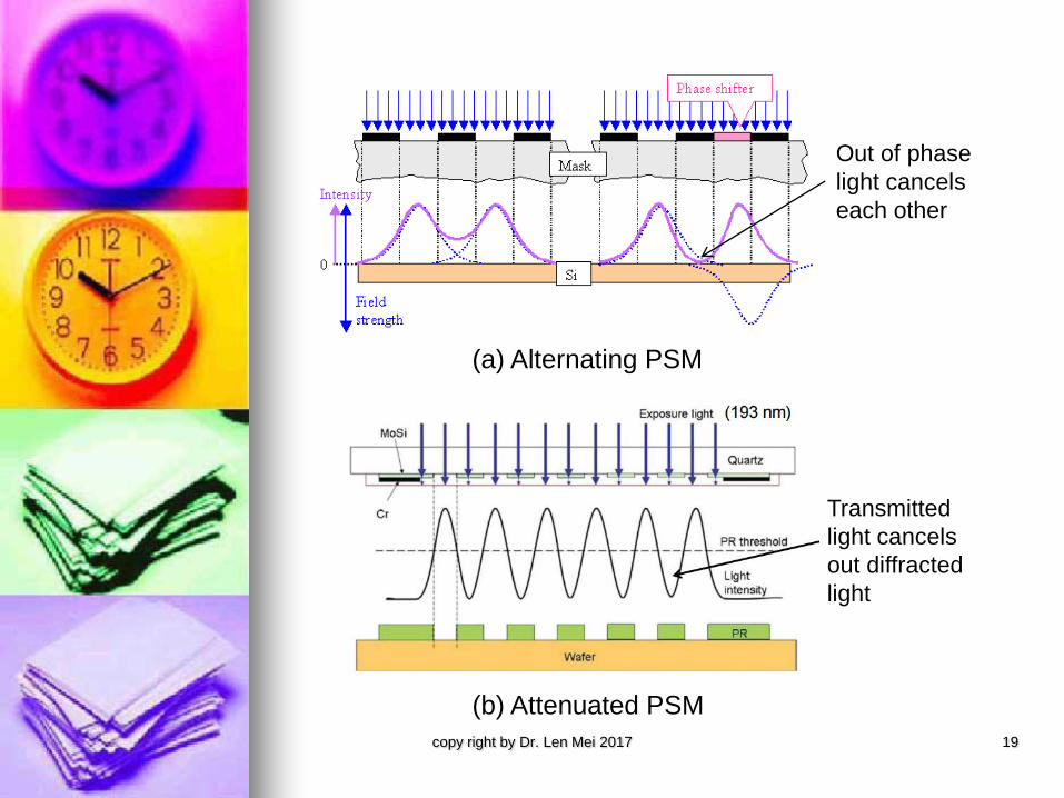
copy right by Dr. Len Mei 2017 19
Transmitted
light cancels
out diffracted
light
Out of phase
light cancels
each other
(a) Alternating PSM
(b) Attenuated PSM
Double Patterning and Multi-
Patterning
DP and MP are lithographic techniques to improve
the resolution by more than one exposure (pitch
splitting technique) or to use the etched feature to
form sidewalls (spacer technique).
Pitch splitting technique involves the division of a
pattern into two or three parts, each of them
processed separately, in the litho-etch-litho-etch
sequence, also known as LELE.
20 2009/07/17
Double Patterning and Multi-
Patterning
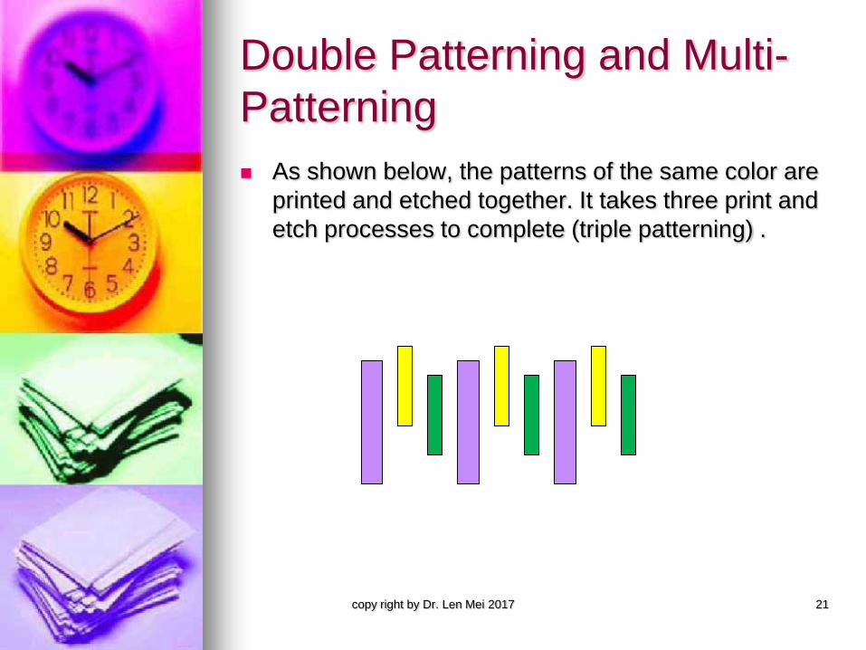
As shown below, the patterns of the same color are
printed and etched together. It takes three print and
etch processes to complete (triple patterning) .
copy right by Dr. Len Mei 2017 21
Double Patterning and Multi-
Patterning
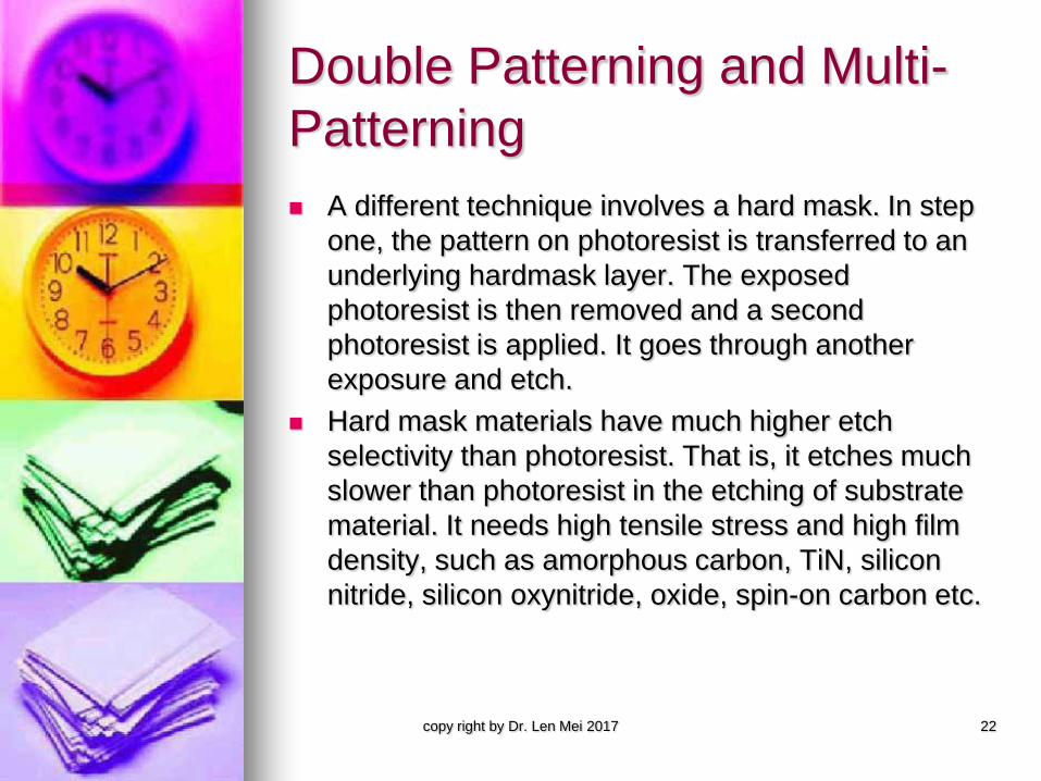
A different technique involves a hard mask. In step
one, the pattern on photoresist is transferred to an
underlying hardmask layer. The exposed
photoresist is then removed and a second
photoresist is applied. It goes through another
exposure and etch.
Hard mask materials have much higher etch
selectivity than photoresist. That is, it etches much
slower than photoresist in the etching of substrate
material. It needs high tensile stress and high film
density, such as amorphous carbon, TiN, silicon
nitride, silicon oxynitride, oxide, spin-on carbon etc.
copy right by Dr. Len Mei 2017 22
Double Patterning and Multi-
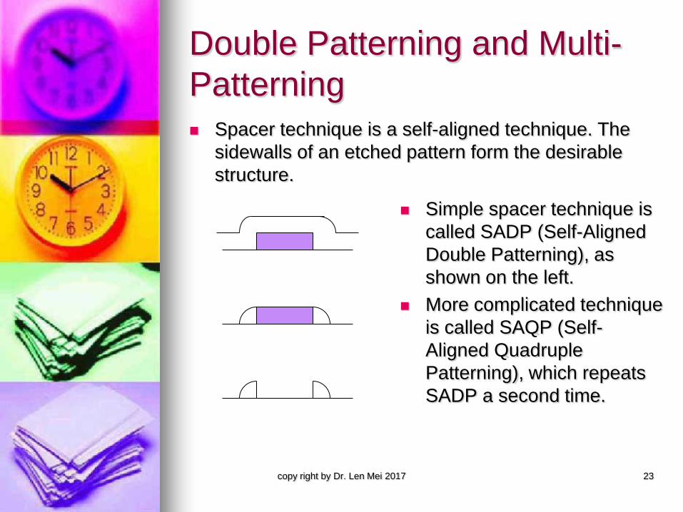
Patterning Spacer technique is a self-aligned technique. The
sidewalls of an etched pattern form the desirable
structure.
copy right by Dr. Len Mei 2017 23
Simple spacer technique is
called SADP (Self-Aligned
Double Patterning), as
shown on the left.
More complicated technique
is called SAQP (Self-
Aligned Quadruple
Patterning), which repeats
SADP a second time.
Double Patterning and Multi-
Patterning
As one can imagine, the use of DP and MP involves
not only the process change but also extensive
work in design.
The steps involved are:
design of DP or MP compliant layout;
design verification;
decomposition of the layout into double or triple layers
OPC steps for each layer
OPC verification for each layer
mask data preparation
mask manufacture
finally processing in the fab, each of these process
step needs to be developed and controlled just like
any other process step.
copy right by Dr. Len Mei 2017 24
Double Patterning and Multi-
Patterning
It introduced many unfavorable factors into the
process.
Cost in more processing steps, more masks, in design,
layout, verification and mask design
Alignment
Process variability.
Cycle time
Testing and debugging
Process tolerance
Additional difficulties are found in design and mask
synthesis (decomposition, RET, OPC and
verification) for compliant layouts.
copy right by Dr. Len Mei 2017 25
Restricted Design Rules
Today, design rules are the only rules designers
need to follow for the physical design and layout.
However, increasing variability in the performance
of the device requires more rules to be imposed.
For example:
Lithographic rounding of the active and the contact in
a source or drain connection can reduce the
alignment marginality
In a gate, horizontal bends in the poly nearby can
induce a variation in the L-effective.
A curvature in the horizontal-to-vertical transition in
the active layer can cause variation in the W-effective.
copy right by Dr. Len Mei 2017 26
Restricted Design Rules
RDR imposes additional restrictions to the existing
design rules.
RDR is based on the concept that a regular array is
significantly easier to manufacture than a random
array of cells.
RDR is a new way of thinking of the design-for-
manufacturability (DFM).
So far, it is aimed at layout rather than design. It
makes changes in physical design like place-and-
route.
But long term wise, new EDA tools, process
equipment or design methodologies will emerge.
copy right by Dr. Len Mei 2017 27
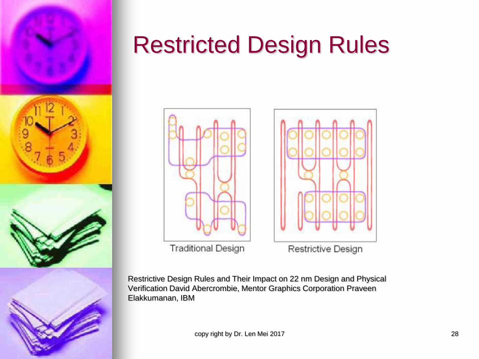
Restricted Design Rules
Restrictive Design Rules and Their Impact on 22 nm Design and Physical
Verification David Abercrombie, Mentor Graphics Corporation Praveen
Elakkumanan, IBM
copy right by Dr. Len Mei 2017 28
Gridded Design Rules
GDR is a special set of the Restricted Design Rules.
As the name implies, the layout is divided into grids,
such as Layout Base Unit (LBU) Grid, Placement
Grid.
The layout objects are line (poly, metal), point
(contact, via), block (diffusion, implant).
All objects need to have vertices on the LBU grids
and anchors (center line of line object, center of
point object, edges of block object) on the
Placement grids.
Following GDR, the layout will be much more
regular and comply to higher DFM.
copy right by Dr. Len Mei 2017 29
Negative Tone Development
In a NTD, the negative tone resist (NTR) is used,
where the exposed resist is polymerized and
becomes insoluble to the developer.
Masks used for negative photoresists contain the
inverse or photographic "negative" of the pattern.
In the early days of the industry, NTR was widely
used. It gradually phased out because of its poor
resolution at smaller feature sizes due to the
exposed and unexposed areas permeated by the
solvent causing pattern distortions.
However, the effect of NTD and PTD (Positive Tune
Development) are not complimentary. This opens
up a window for optimizing the resist system.
copy right by Dr. Len Mei 2017 30
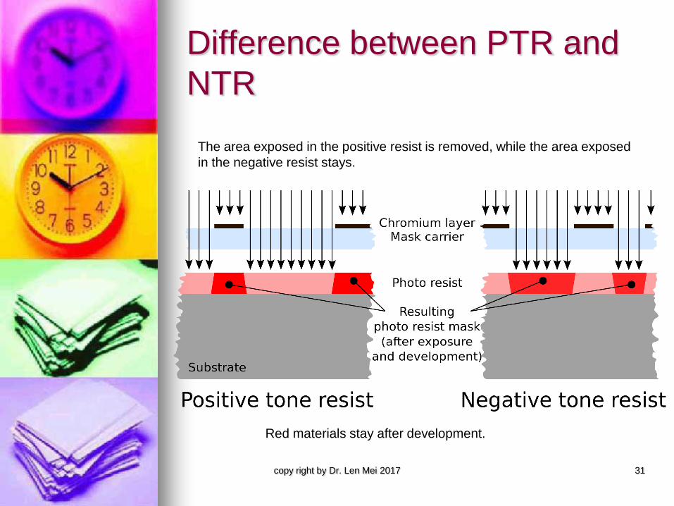
Difference between PTR and
NTR
copy right by Dr. Len Mei 2017 31
The area exposed in the positive resist is removed, while the area exposed
in the negative resist stays.
Red materials stay after development.
Negative Tone Development
With the advance in negative tone development
technology, the industry has found renewed interest
in the NTD.
NTR can print isolated and densely packed lines at
the same line width, while PTR has up to 10% of
nominal line width due to the imaging property of lens.
NTR also provides advantages to the isofocus bias –
the variation in CD due to exposure and focus
combination.
NTR provides low swelling and smooth- dissolving
behavior during development, therefore, better line
edge roughness (LER).
Due to the above advantages, NTR is superior in
double patterning process.
copy right by Dr. Len Mei 2017 32
Negative Tone Development
NTR processing such as the pre-applied bake (PAB)
temperature, post-exposure bake (PEB) temperature,
development procedure, and rinse procedure are very
effective for improving the lithographic performance.
NTR enables the printing of dark field features on
wafer using bright field masks with a better
manufacturing capability for back-end-of-line
processing.
However, NTR is not cure for all. For example, for
contact layer, NTR has smaller depth of focus.
The ability to choose the right tone may play an
important role in optimizing the process.
copy right by Dr. Len Mei 2017 33
Technology development at
equipment vendor side
copy right by Dr. Len Mei 2017 34
Evolution of Photolithography
tools
Effort to improve resolution.
Change of wavelength is no trivial task…
Change in optics
Change in photoresist system
Change in mask system
35 2009/07/17
Theoretically,
To improve resolution, we need to
Reduce wavelength (248 nm , 193 nm, 13.5 nm)
Increase refraction index (air to water)
Increase focal point angle (OAI)
To improve depth of focus, we need to
Increase refraction index
Increase focal point angle
To improve contrast, we need to
Widen minimum to maximum intensity
At the same time, we have to achieve
Overlay requirement: 20% of half pitch
CD uniformity: 7% of half pitch
copy right by Dr. Len Mei 2017 36
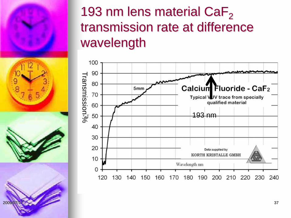
193 nm lens material CaF2
transmission rate at difference
wavelength
37 2009/07/17 T
ransm
issio
n %
193 nm
Next generation scanners:
EUV Extreme ultraviolet lithography (EUV) is the next
generation lithography technology.
Current schedule for high volume production use by
2020.
EUV at the 5 nm node will require a
higher numerical aperture and multiple patterning.
EUV exposure takes longer time due to source
power limitations.
38 2009/07/17
Energy required to generate
light
As of 2016, a 125W source enables a wafer
throughput of 85 WPH at an exposure dose of 20
mJ/cm2 (as compared to the immersion tool at 275
WPH with a 125W source).
If 40 mJ/cm2 is needed, it would require 250W
source to maintain 85 WPH.
The current EUV light source is a laser-pulsed Sn
plasma.
The light generating efficiency is low, because:
Sn+ ions in the plasma are unstable. They also absorb
the light they emit, and are easily neutralized by
electrons in the plasma to produce light at unusable
wavelengths.
copy right by Dr. Len Mei 2017 39
EUV light source
In addition, the plasma-based EUV sources are not
coherent. Further energy is lost by converting it into
partially coherent by filtering.
Therefore, EUV light source needs to be at least
10kW vs. 193 nm light source of 100 W, a 100 fold
increase. This dramatically increases the utility bill
to operate EUV scanner.
The collector in the light source is exposed to the
plasma, which deposits Sn on the collector surface
and degrades the reflectivity. It has to be clean
regularly.
Sn contamination affects not only the light output
but also cost of ownership because of costly and
time-consuming cleaning or replacing.
copy right by Dr. Len Mei 2017 40
EUV optical system and mask
EUV is strongly absorbed by any media, so the EUV
optical system from light source to wafer must be in
vacuum.
EUV optical system has to use mirror instead of
lens with multilayer reflective coatings.
The mask also must be reflective, essentially a
patterned mirror.
The incidence EUV has only 70% of reflectivity.
Much of the light is lost in reflectivity through several
mirrors and mask.
It is estimated that only 1/26th of the photons arrived
at the wafer.
copy right by Dr. Len Mei 2017 41
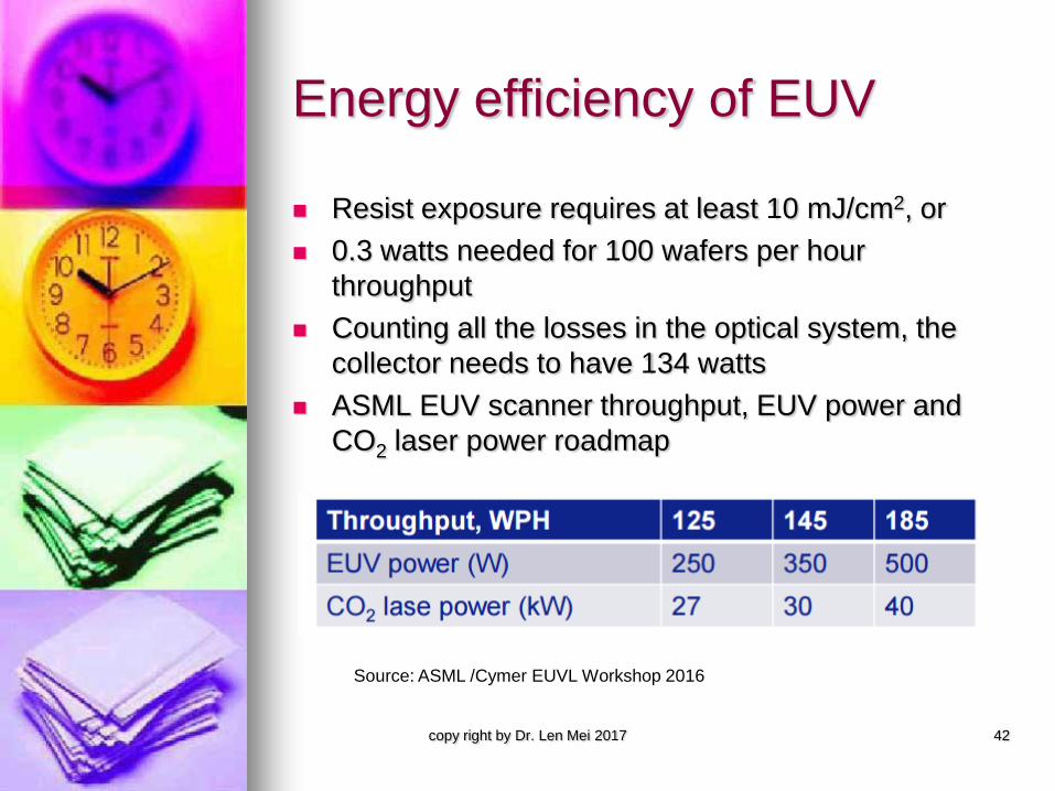
Energy efficiency of EUV
Resist exposure requires at least 10 mJ/cm2, or
0.3 watts needed for 100 wafers per hour
throughput
Counting all the losses in the optical system, the
collector needs to have 134 watts
ASML EUV scanner throughput, EUV power and
CO2 laser power roadmap
copy right by Dr. Len Mei 2017 42
Source: ASML /Cymer EUVL Workshop 2016
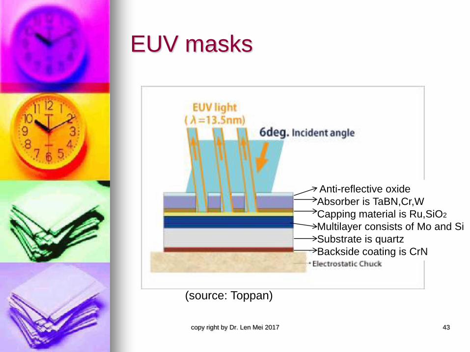
EUV masks
copy right by Dr. Len Mei 2017 43
(source: Toppan)
Anti-reflective oxide
Absorber is TaBN,Cr,W
Capping material is Ru,SiO2
Multilayer consists of Mo and Si
Substrate is quartz
Backside coating is CrN
EUV masks
By nature, EUV mask must absorb the light on the
dark pattern so that the light will not be sent to
wafer. Depending on the area where light is not to
be reflected, it can absorb a large percentage of the
light, so gets hot, may cause distortion.
The multilayer consists of 40-50 layers of alternating
4.1 nm of silicon and 2.8 nm of molybdenum then a
capping layer of ruthenium on top to prevent
oxidization.
The EUV absorber on the dark patterns is a
tantalum boron nitride film topped with an anti-
reflective oxide.
With such a complicated structure, it is prone to
defects.
copy right by Dr. Len Mei 2017 44
EUV masks
The biggest defect comes with the blanks. To
overcome the problem, mask makers locate the
defects on the blank, and during the e-beam
patterning of the mask, it avoids the defect using
pattern shifting techniques.
The writing of whole mask using single ebeam can
take 50 to 100 hours, so the multi-ebeam writing
tool is developed.
The mask is also susceptible to the constant
exposure of EUV light.
copy right by Dr. Len Mei 2017 45
EUV masks
EUV mask ecosystem, including blanks, pellicles
and inspection, are also radically different.
Particle contamination would be significant since
current pellicles are not stable above the targeted
power for manufacturing at 200 W.
Without pellicles, particle adders would reduce
yield.
The current lack of any suitable pellicle material,
aggravated by the use of hydrogen plasma cleaning
in the EUV scanner presents an obstacle to volume
production.
46 2009/07/17
EUV masks
As usual, pellicle imposes a big challenge to the
EUV mask, since any material absorbs EUV light. It
not only reduces the light intensity to reach the
wafer but also heats up to quite high temperature
>600oC.
ASML, the sole supplier of EUV pellicles in the
industry right now, is developing a 50 nm thick
polysilicon-based EUV pellicle, which is retractable
for inspection.
copy right by Dr. Len Mei 2017 47
Resist system
Photon energy hν for
248 nm, KrF laser is 5 ev
193 nm, ArF laser is 6.4 ev
13.5 nm, CO2 laser generated Sn+ plasma is 91 ev
Such high energy photons generate secondary
electrons, known as resist flare, which degrades the
image quality.
Other issues such as resist collapse at fine
geometry and stochastic effects (including photon
shot noise), also prevent EUV from exceeding the
resolution limits of immersion lithography in high
volume manufacturing.
copy right by Dr. Len Mei 200907 48 2009/07/17
Resist system
To boost the EUV throughput without increasing the
light source power is to improve the resist
sensitivity, however, it is done at the expense of
LWR and resolution.
DUV resist receives 100 mJ/cm2. EUV resist
operates below 30 mJ/cm2.
When the photon dose goes lower, the line-width
roughness quickly deteriorates.
Double patterning is expected for EUV for random
logic patterns at the 7 nm node.
The 5 nm node would need to use multiple
patterning.
copy right by Dr. Len Mei 2017 49
Other challenges of EUV
With radically different source and optics, EUV
scanners have special overlay concerns.
Since Electrostatic chuck is used, flatness on the
backside of mask can be transferred into the front
side after chucking.
Defects larger than 1 μm can exert different
pressure on the mask and they can also migrate to
the backside of mask.
Distortion can cause registration error.
Vacuum in the optical assembly leads to heating of
the wafer without much dissipation. A sacrificial first
wafer was found to be necessary to stabilize the
chuck temperature. Thus, an extra wafer per lot is
required for overlay stabilization in EUV lithography.
copy right by Dr. Len Mei 2017 50
Other challenges
The use of reflection causes wafer exposure
position to be extremely sensitive to the reticle
flatness and the reticle clamp.
The off-axis illumination of the reticle is also the
cause of non-telecentricity in wafer defocus, which
consumes most of the overlay budget of the EUV
scanner.
copy right by Dr. Len Mei 2017 51
EUV cost of ownership
Even though EUV scanner is extremely expensive
to buy (>$90 m per unit), to operate and to maintain,
plus the cost of expensive mask and resist system,
but there is little choice when working on technology
nodes <7 nm.
On the other hand, one EUV step can replace
several DUV steps.
copy right by Dr. Len Mei 2017 52
Perspectives
Despite all the challenges, the industry manages to
bring EUV photolithographic technology into
production.
The leading companies, such as Intel, TSMC,
Samsung all plan to introduce EUV technology into
their production starting 2017.
This will help to move the mass production
technology node into 7 nm in 2018 and 5 nm in
2020.
copy right by Dr. Len Mei 2017 53