Embed Size (px)
DESCRIPTION
PCB stands for Printed Circuit Boards. HPCB PCB manufacturer specializes in prototype to medium production volumes. With our speedy and strong engineering support, we can provide simple solutions to complex design issues. Just simply send a Gerber file to us; we come back with the PCB of your choice with the stated time frame.
Citation preview
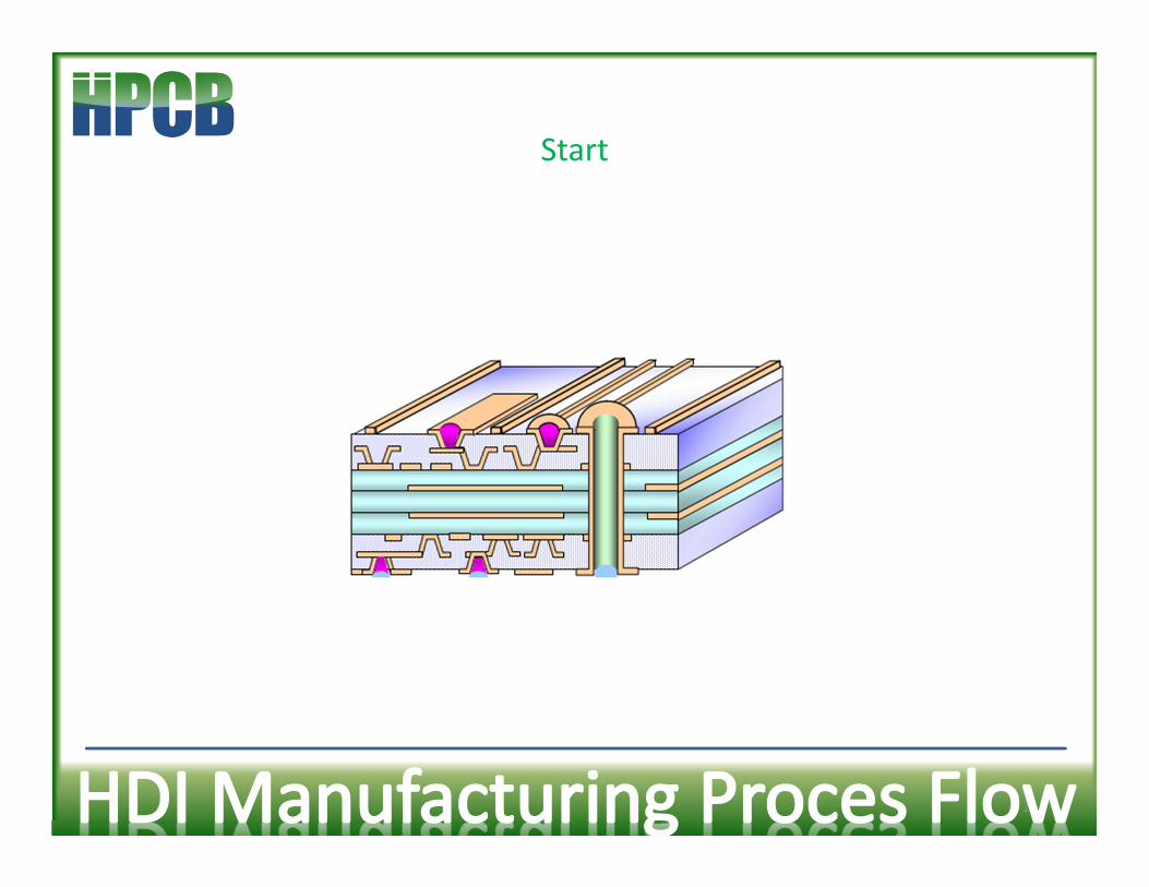
Start
1

2
Pre-engineering
Pattern imaging
Etching
Laminating
Drilling
Cu plating
Hole plugging
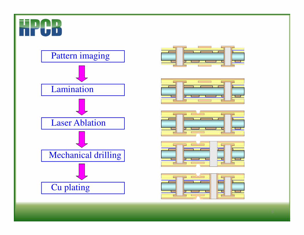
Pattern imaging
Lamination
Laser Ablation
Mechanical drilling
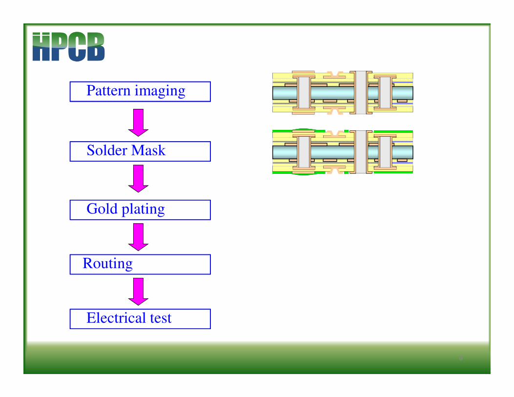
Pattern imaging
Cu plating
Solder Mask
Surface Finished
Routing
Visual inspection
Electric test
Shipping

Pre-engineering
Pattern imaging
Etching
Laminating
Drilling
3

4
Desmear
Cu plating
Hole plugging
Cu plating
Belt Sanding
Lamination
Laser Ablation
Mechanical drilling
Cu plating
Pattern imaging
5
6
Solder Mask
Gold plating
Routing
Electrical test
Pattern imaging

7
Hole counter
Shipping
Visual inspection

8
* Raw material (Thin Core,Copper,Prepreg…...)
Raw Material Raw Material Raw Material Raw Material : : : : FRFRFRFR----4 (4 (4 (4 (Difuntional,TetrafuntionalDifuntional,TetrafuntionalDifuntional,TetrafuntionalDifuntional,Tetrafuntional))))Supplier Supplier Supplier Supplier : EMC ,Nan: EMC ,Nan: EMC ,Nan: EMC ,Nan----YaYaYaYaSheet sizeSheet sizeSheet sizeSheet size : 36: 36: 36: 36”*48*48*48*48” , 40, 40, 40, 40”*48*48*48*48” ,42,42,42,42”*48*48*48*48Core ThicknessCore ThicknessCore ThicknessCore Thickness : 0.003: 0.003: 0.003: 0.003”,0.004,0.004,0.004,0.004”,0.005,0.005,0.005,0.005”,0.006,0.006,0.006,0.006”
0.0080.0080.0080.008”,0.010,0.010,0.010,0.010”,0.012,0.012,0.012,0.012”,0.015,0.015,0.015,0.015”
0.0210.0210.0210.021”,0.031,0.031,0.031,0.031”,0.039,0.039,0.039,0.039”,0.047,0.047,0.047,0.047”
Copper Foil Copper Foil Copper Foil Copper Foil : 1/3 : 1/3 : 1/3 : 1/3 oz,1oz,1oz,1oz,1/2 /2 /2 /2 oz,1.0oz,1.0oz,1.0oz,1.0 oz,2oz,2oz,2oz,2 ozozozozPrepregPrepregPrepregPrepreg type type type type : 1080,2113,2116,1506,7628,7630: 1080,2113,2116,1506,7628,7630: 1080,2113,2116,1506,7628,7630: 1080,2113,2116,1506,7628,7630
9
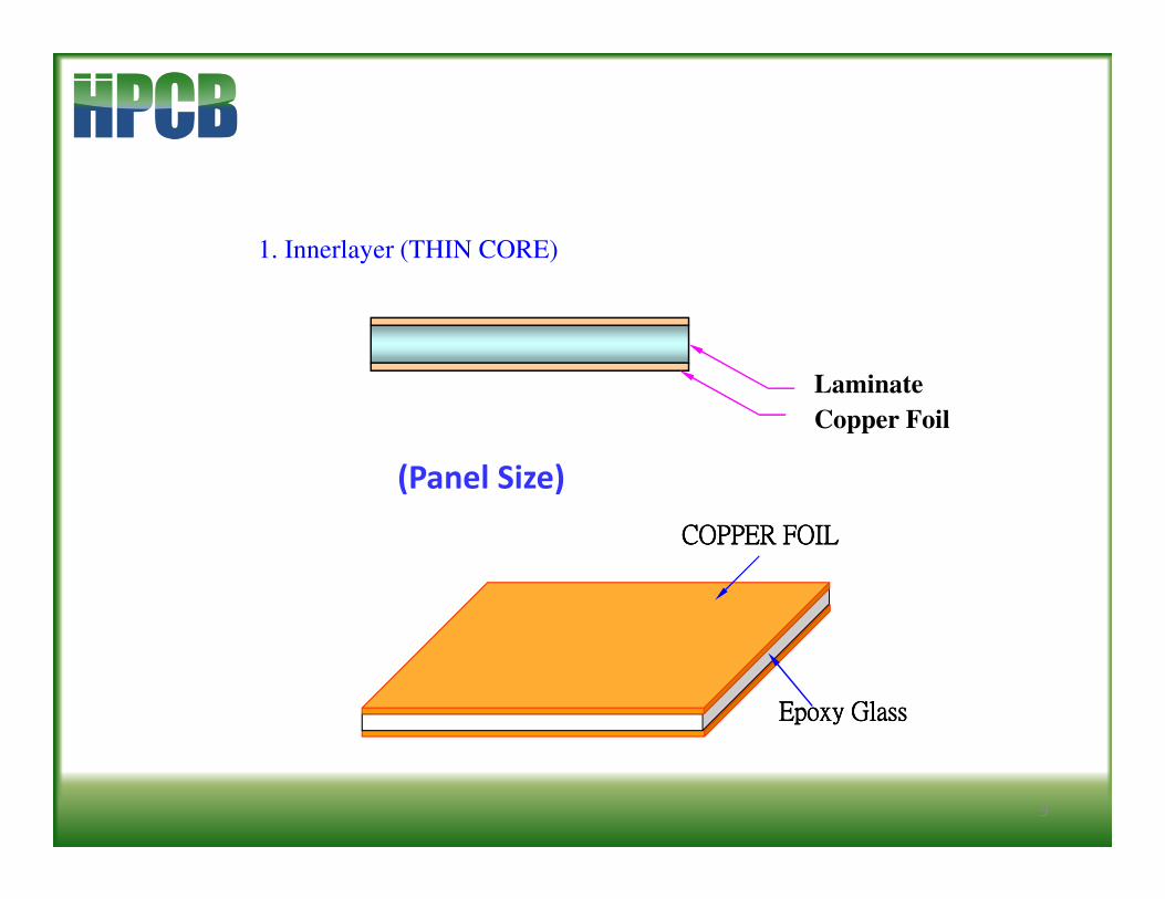
1. Innerlayer (THIN CORE)
Laminate
Copper Foil
(Panel Size)
COPPER FOILCOPPER FOILCOPPER FOILCOPPER FOIL
Epoxy GlassEpoxy GlassEpoxy GlassEpoxy Glass
10
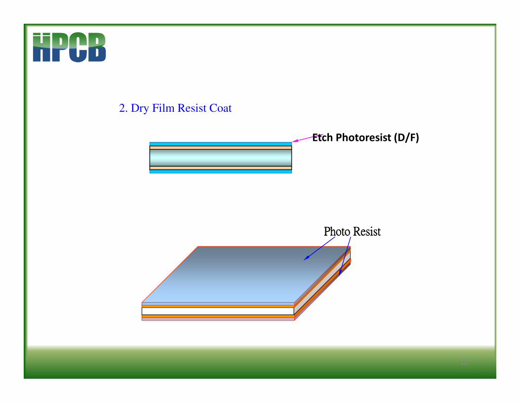
Photo ResistPhoto ResistPhoto ResistPhoto Resist
2. Dry Film Resist Coat
Etch Photoresist (D/F)
11
Photo ResistPhoto ResistPhoto ResistPhoto Resist
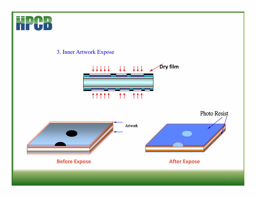
3. Inner Artwork Expose
Dry film
ArtworkArtworkArtworkArtwork
After ExposeBefore Expose
12
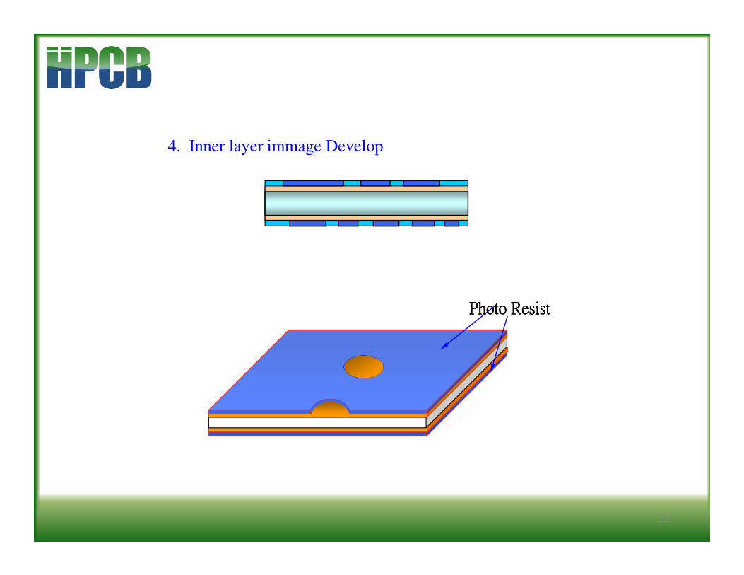
4. Inner layer immage Develop
Photo ResistPhoto ResistPhoto ResistPhoto Resist
13
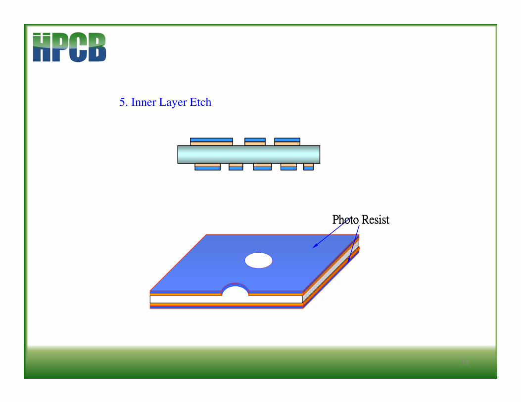
5. Inner Layer Etch
Photo ResistPhoto ResistPhoto ResistPhoto Resist

14
6. Inner Layer Strip Resist

15
7. Oxide Coating

16
8. Lay-up Building
LAYER 2
LAYER 3
LAYER 4
LAYER 5
LAYER 1
LAYER 6
Layer 1
Layer 2
Layer 3
Layer 4
Copper Foil
Copper Foil
Inner Layer
Prepreg
Prepreg

17
9. Lamination

18
.
.
.
COPPER FOIL 0.5 OZ
Thin Core ,FR-4prepreg
COMP
S0LD.
prepreg
Thin Core ,FR-4prepreg
COPPER FOIL 0.5 OZSuperimposed with the steel
10101010----12121212層疊合層疊合層疊合層疊合
The hot plate press machine
COPPER FOIL 0.5 OZ
Thin Core ,FR-4prepreg
COMP
S0LD.
prepreg
Thin Core ,FR-4prepreg
COPPER FOIL 0.5 OZ
The hot plate press machine
Superimposed with the steel
• Superimposed with the steel
Typical of the multilayer structure of stacked plates and laminated
Superimposed with the steel

19
board
Alu
base
10. NC Drilling

20
11. Desmear & Copper Deposition

21
12. Hole Plugging
13. Belt Sanding

22
14. Copper Reduction → Option
15. Belt Sanding → Option
23
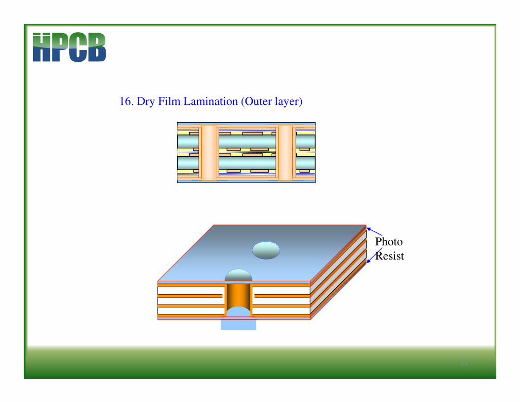
16. Dry Film Lamination (Outer layer)
Photo
Resist

24
17. Outerlayer Expose
UV
25
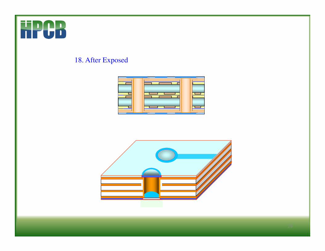
18. After Exposed

26
19. Outerlayer Develop
27
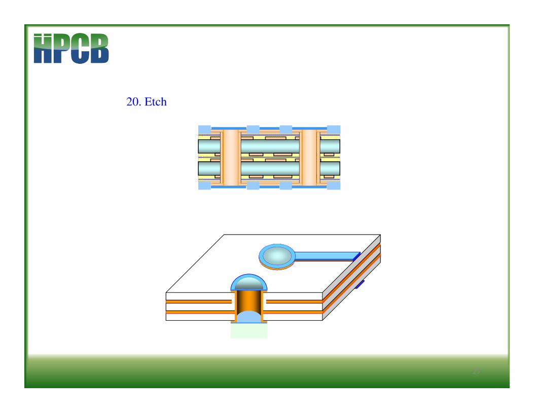
20. Etch
28
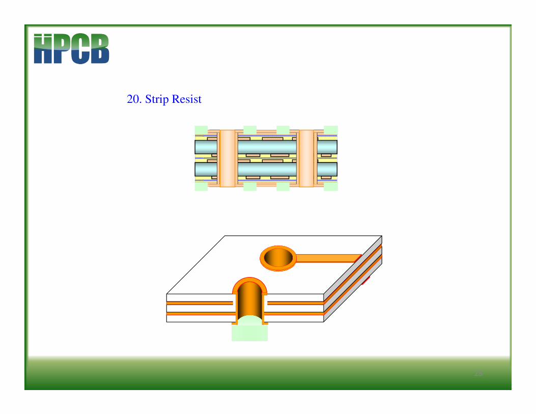
20. Strip Resist

29
21. Build-up Layer Lamination
RCCRCCRCCRCC((((RRRResin esin esin esin CCCCoated oated oated oated CCCCopper opper opper opper foil)foil)foil)foil)
30
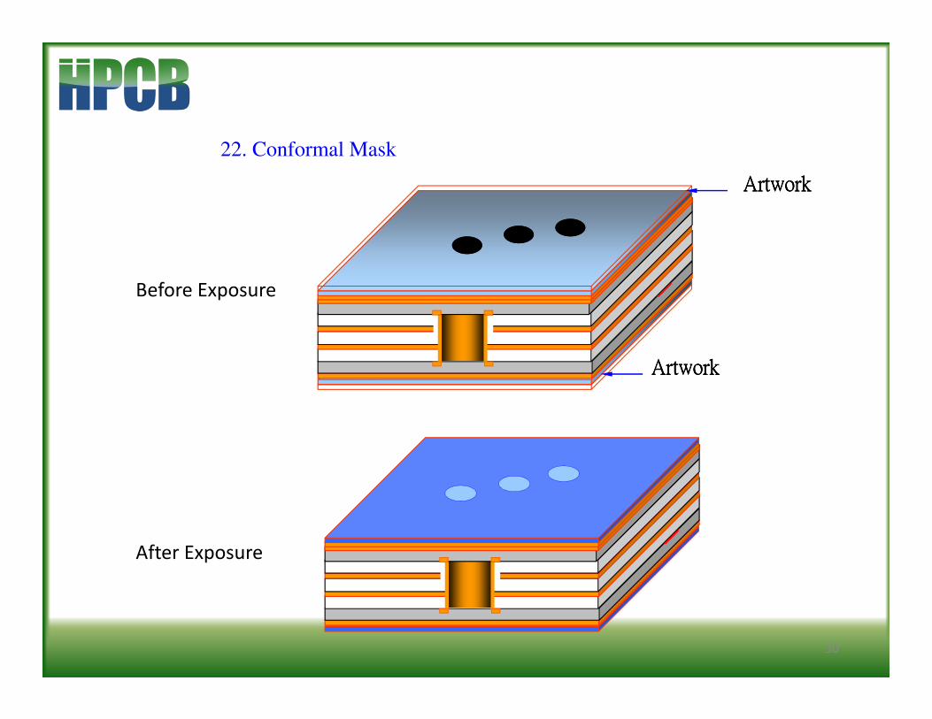
ArtworkArtworkArtworkArtwork
ArtworkArtworkArtworkArtwork
22. Conformal Mask
Before Exposure
After Exposure
31
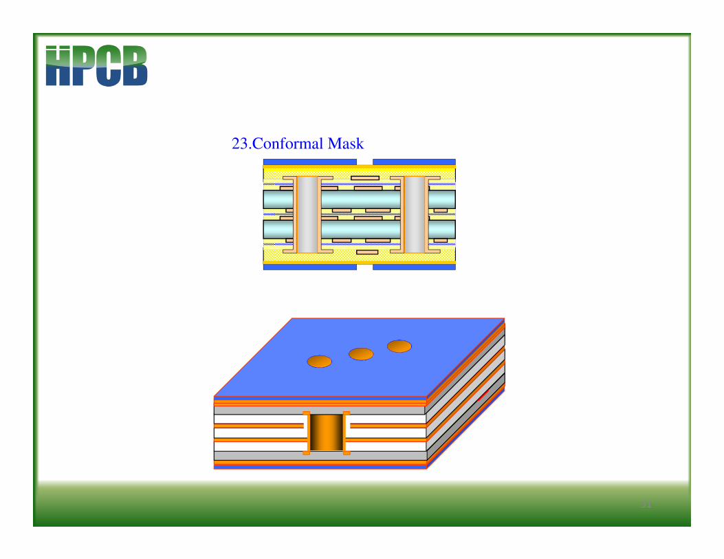
23.Conformal Mask
32
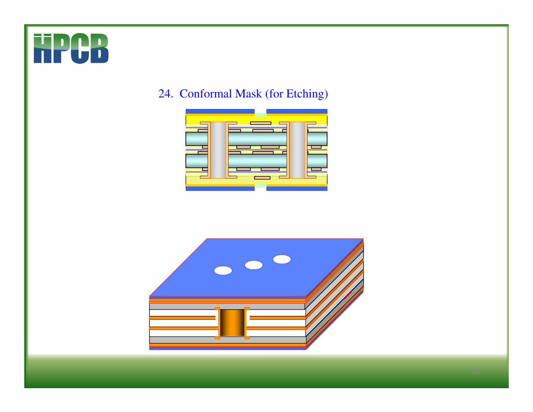
24. Conformal Mask (for Etching)
33
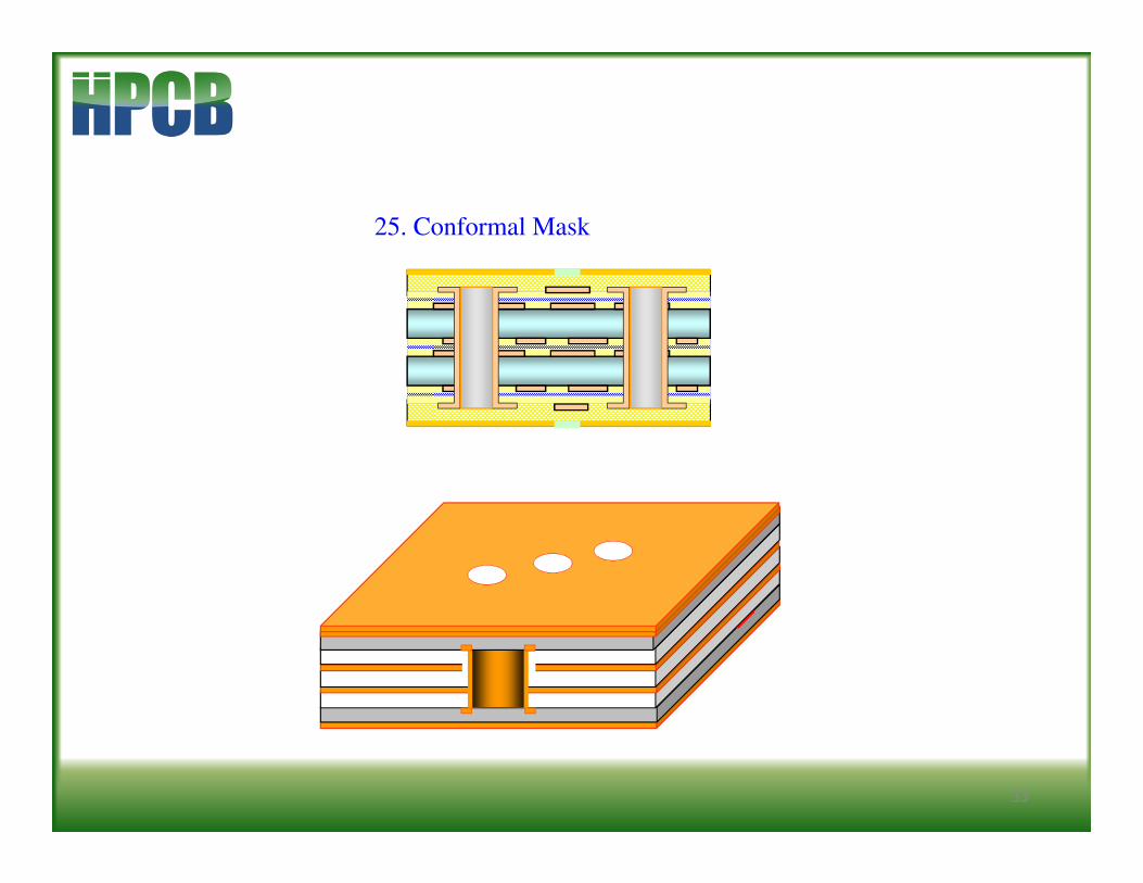
25. Conformal Mask
34
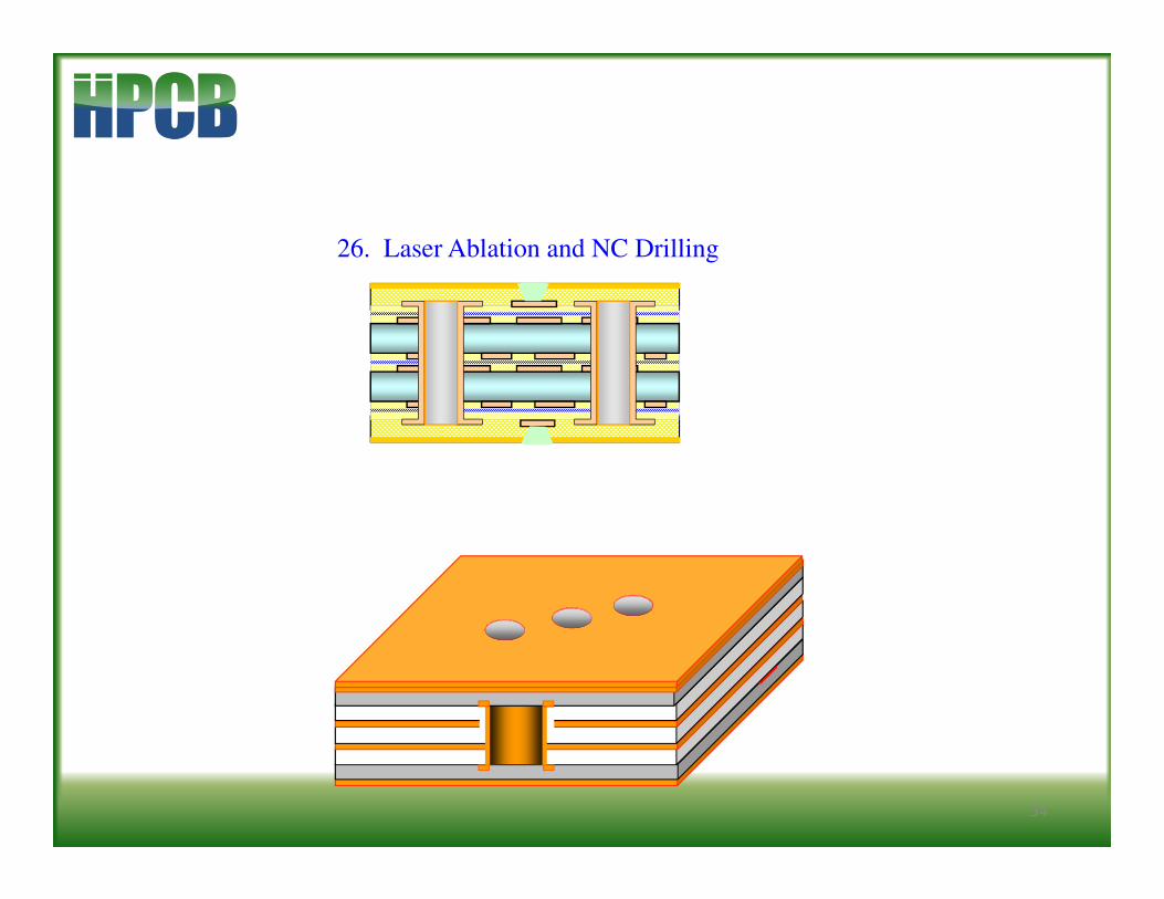
26. Laser Ablation and NC Drilling

35
Mechanical Drill(P.T.H.)
Laser Microvia(Blind Via)
27. Mechanical Drill

36
28. Desmear & Copper Deposition

37
29. Outerlayer Pattern imaging)
Dry Film Lamination)
38
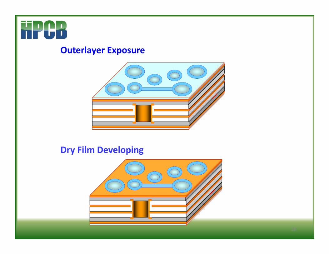
Outerlayer Exposure
Dry Film Developing
39
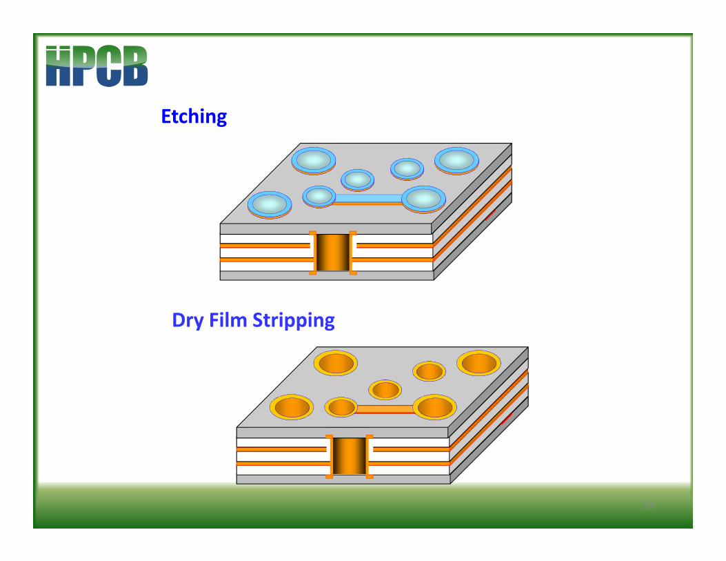
Etching
Dry Film Stripping
40
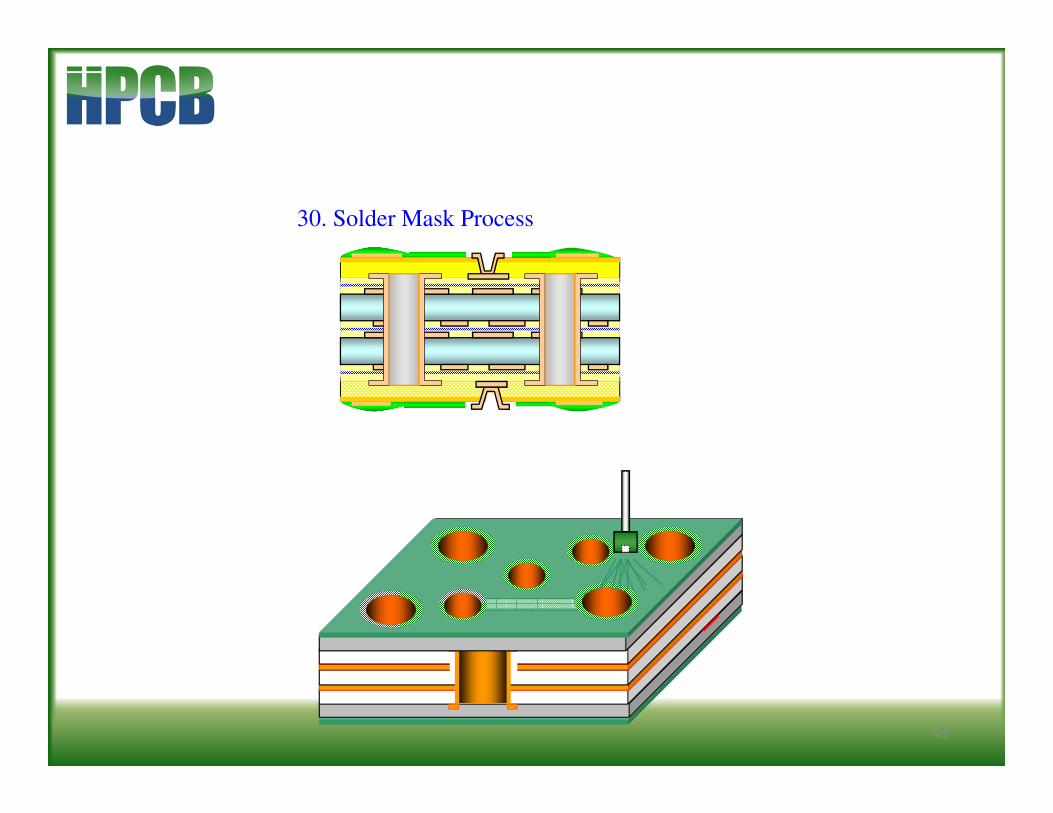
30. Solder Mask Process
41
HPCB94V-0
R305
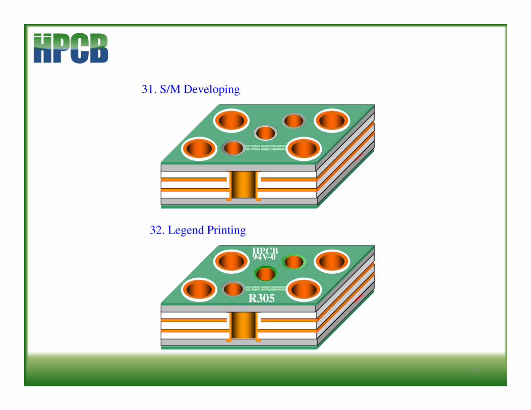
31. S/M Developing
32. Legend Printing

42
33. Electroless Ni/Au , HAL_lead free and Etc.
R305
HPCB94V-0
43
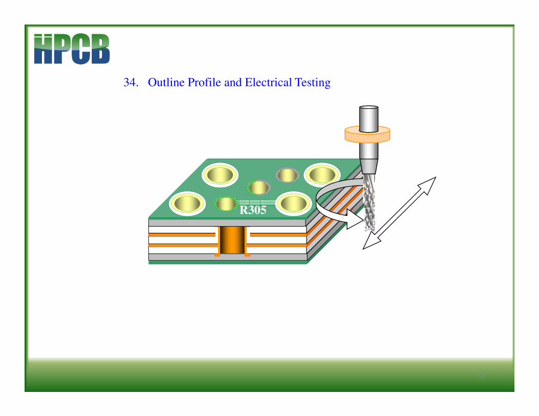
R305
34. Outline Profile and Electrical Testing
• HPCB• 94V-0

44
R305
R305
36. Final Inspection
37. O.S.P. (Entek plus Cu_106A….) →Option
• HPCB• 94V-0
• HPCB• 94V-0

45
LASER BLIND & BURIED VIA LAY-UP
A = THROUGH VIA HOLE
B = BURIED VIA HOLE
C = One Level Laser Blind Via
LASER BLIND & BURIED VIA LAY-UP
BURIED VIA AND LASER BLIND VIA OPTION
D
C
C
D = Two Level Laser Via
CD
C
BBBB----STAGESTAGESTAGESTAGE
FR-4 Core
RCC
FR-4 Core
BBBB----STAGESTAGESTAGESTAGE
RCC
A BB A

46
BURIED VIA LAY-UP
A = THROUGH VIA HOLE
B = BURIED VIA HOLE
C = BLIND VIA HOLE
D = BLIND HOLE MLB VIA
BLIND VIA LAY-UP
BLIND VIA SEQUENTIAL LAY-UP
A
B
B
A
R
E
S
I
N
B-STAGE
BLIND AND BURIED VIA OPTION
D
A
C
C
E

47
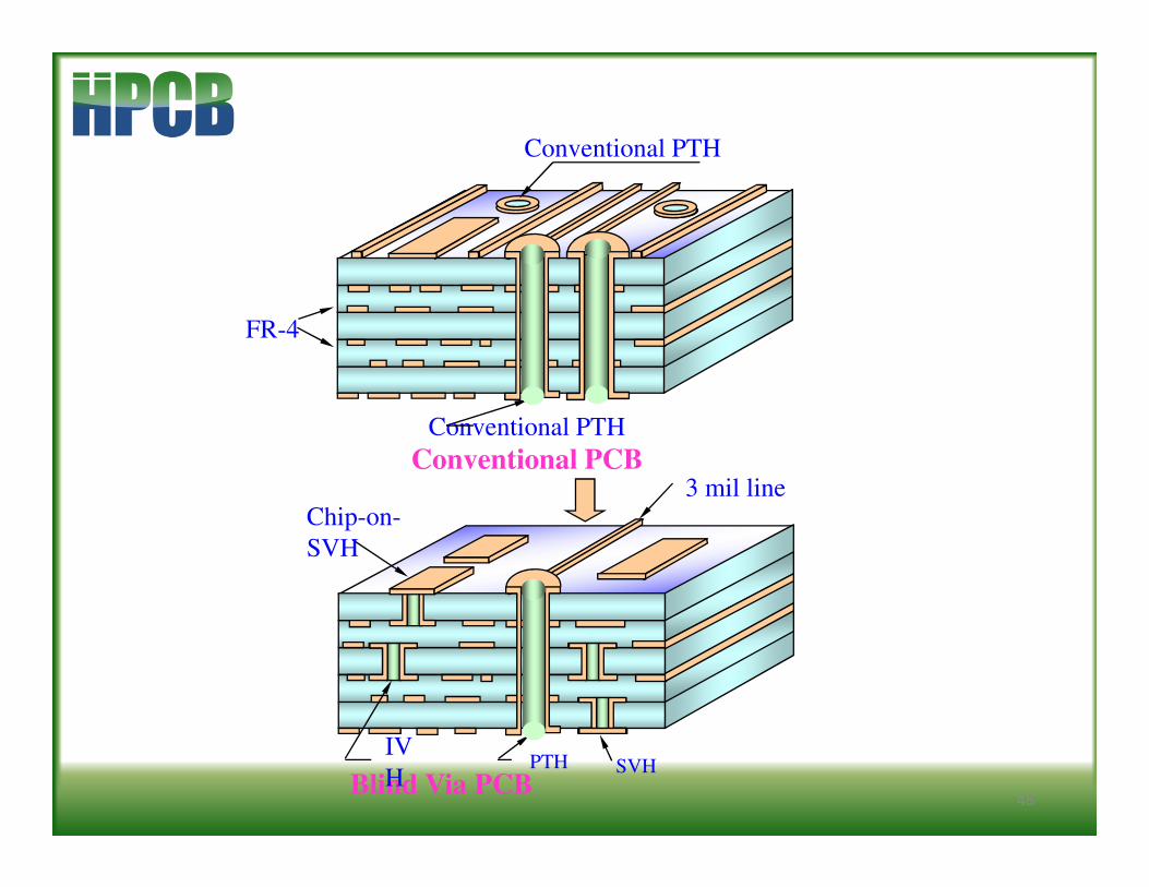
Conventional PCB
FR-4
Build-up
Layer
Build-up
Layer
Photo-viaPhoto-Imageable Dielectric (PID)
FR-4
Conventional PTH
Conventional PTH
48
Conventional PCB
Blind Via PCBPTH
3 mil line
SVHIV
H
Chip-on-
SVH
FR-4
Conventional PTH
Conventional PTH
End
49


![Temperature Effects in Automotive-Grade High Speed ... · the PCB manufacturer, the PCB substrate has an εrof approximately 3.6 and a loss tangentof 0.0117 [6]. In this paper we](https://img.pdfslide.net/doc/110x75/5e82b1b4f3308f35272e3bd8/temperature-effects-in-automotive-grade-high-speed-the-pcb-manufacturer-the.jpg)