Embed Size (px)
Citation preview

RFRF generation chain generation chain

RF chain schematic

RF exciter module

Functions of the Distribution board
Distributes the RF signal to 31 numbers of individual CSM PAs.
Routes the RF signal received from the Encoder board to the dedicated PA module for phase control.
Routes the VINT DC to the PAs for MOSFET H-bridge control.
Routes the status of the PA modules to control system through 4253 card #1 by polling method.
The daughter board mounted on the distribution board decodes the 4th state command signals received from the Encoder board and distributes the it to the individual CSM PAs after providing necessary optical isolation.

Remote distribution card
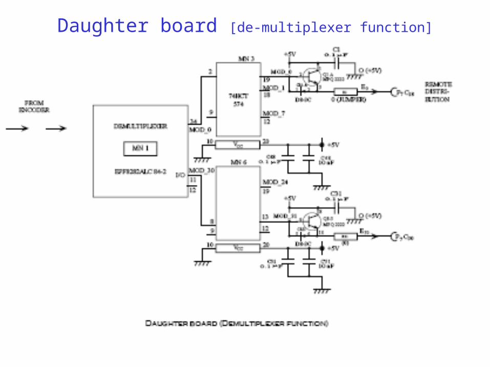
Daughter board [de-multiplexer function]

Daughter board [coupling function]
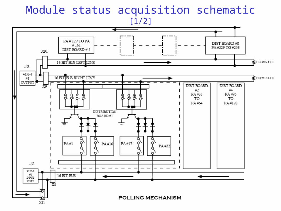
Module status acquisition schematic [1/2]
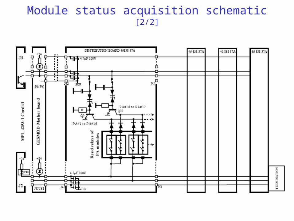
Module status acquisition schematic [2/2]

Switching control for dedicated modules
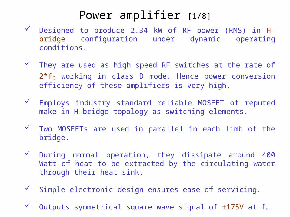
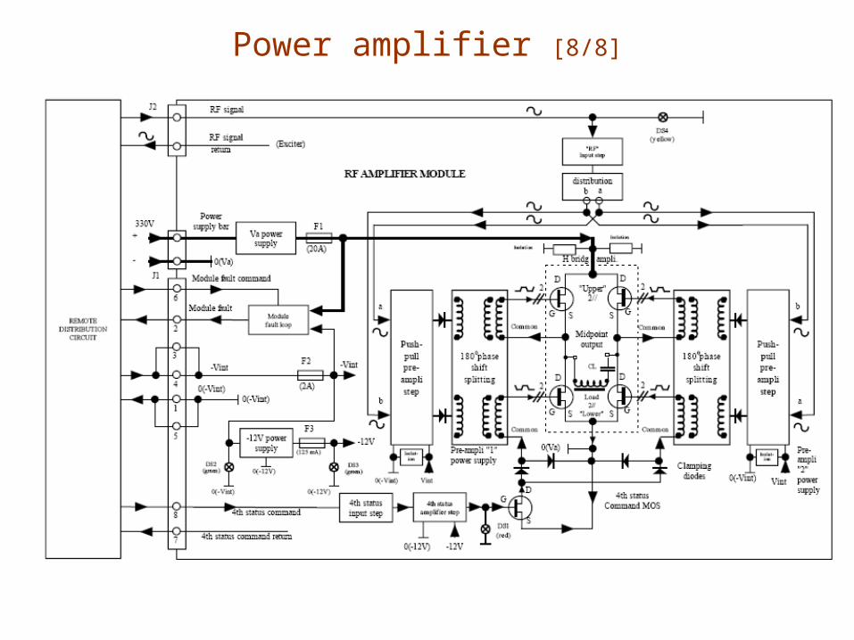
Power amplifier [1/8] Designed to produce 2.34 kW of RF power (RMS) in H-bridge
configuration under dynamic operating conditions.
They are used as high speed RF switches at the rate of 2*fc working in class D mode. Hence power conversion efficiency of these amplifiers is very high.
Employs industry standard reliable MOSFET of reputed make in H-bridge topology as switching elements.
Two MOSFETs are used in parallel in each limb of the bridge.
During normal operation, they dissipate around 400 Watt of heat to be extracted by the circulating water through their heat sink.
Simple electronic design ensures ease of servicing.
Outputs symmetrical square wave signal of ±175V at fc.
Provided with ultra fast fuse to isolate the H-bridge in case of failure of MOSFET to prevent over loading of drain power supply (+330V).
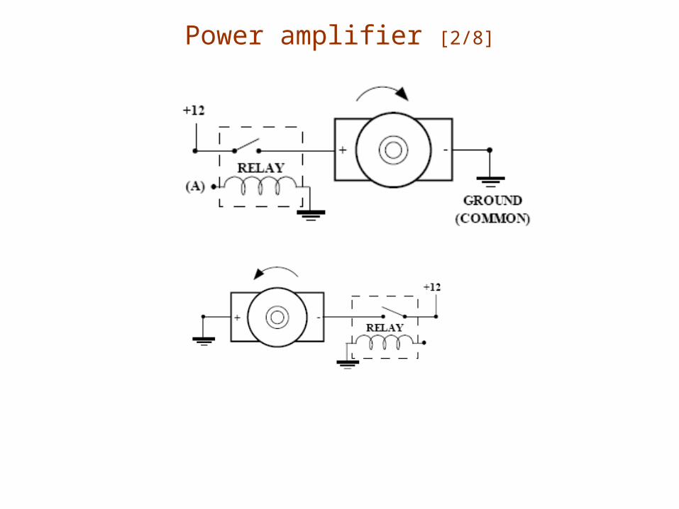
Power amplifier [2/8]
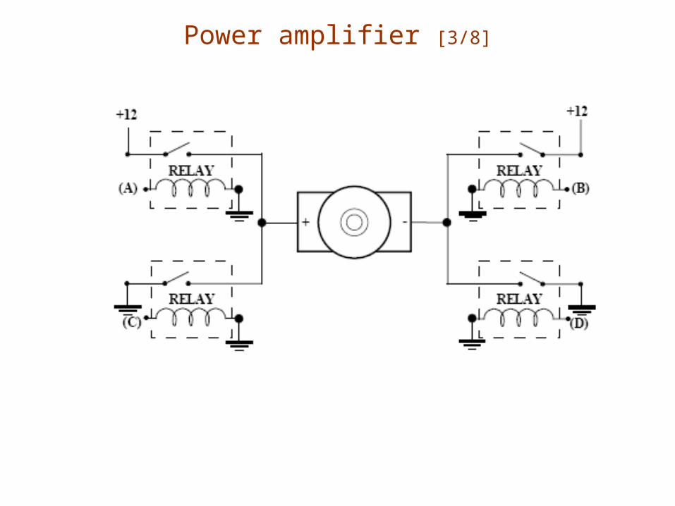
Power amplifier [3/8]

Power amplifier [4/8]
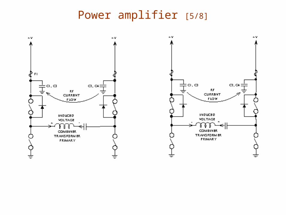
Power amplifier [5/8]

Power amplifier [6/8]
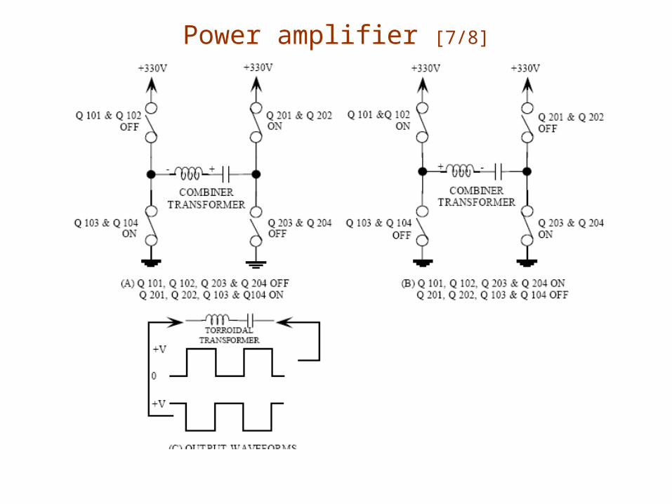
Power amplifier [7/8]
Power amplifier [8/8]

Dedicated module Number
Module position
Proportionate output
1 32 5.1 0.3
2 160 4.7 0.3
3 64 3.8 0.3
4 192 3.1 0.3
5 96 2.3 0.3
6 224 1.6 0.3
7 128 1.0 0.3
8 256 (not used)
0
Dedicated module distribution
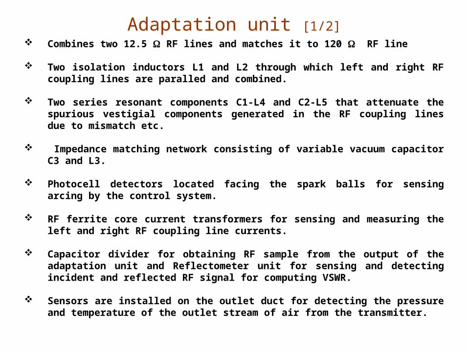
Adaptation unit [1/2] Combines two 12.5 RF lines and matches it to 120 RF line
Two isolation inductors L1 and L2 through which left and right RF coupling lines are paralled and combined.
Two series resonant components C1-L4 and C2-L5 that attenuate the spurious vestigial components generated in the RF coupling lines due to mismatch etc.
Impedance matching network consisting of variable vacuum capacitor C3 and L3.
Photocell detectors located facing the spark balls for sensing arcing by the control system.
RF ferrite core current transformers for sensing and measuring the left and right RF coupling line currents.
Capacitor divider for obtaining RF sample from the output of the adaptation unit and Reflectometer unit for sensing and detecting incident and reflected RF signal for computing VSWR.
Sensors are installed on the outlet duct for detecting the pressure and temperature of the outlet stream of air from the transmitter.

Adaptation unit [2/2]

RF Filter unit [1/2]
A matching circuit made up of L1 coil and C1 capacitor (partial) assembly.
A low pass filter network consisting of C1 capacitor (partial), L2, C2 and C3.
Spark gap placed across each capacitor assembly.
Arrangement for grounding the filter output
Photocell detectors looking into the spark gap for detecting arcing. This information is communicated to control system (Gesmod) for blocking the transmitter in the event of flash or arcing.

RF Filter unit [2/2]
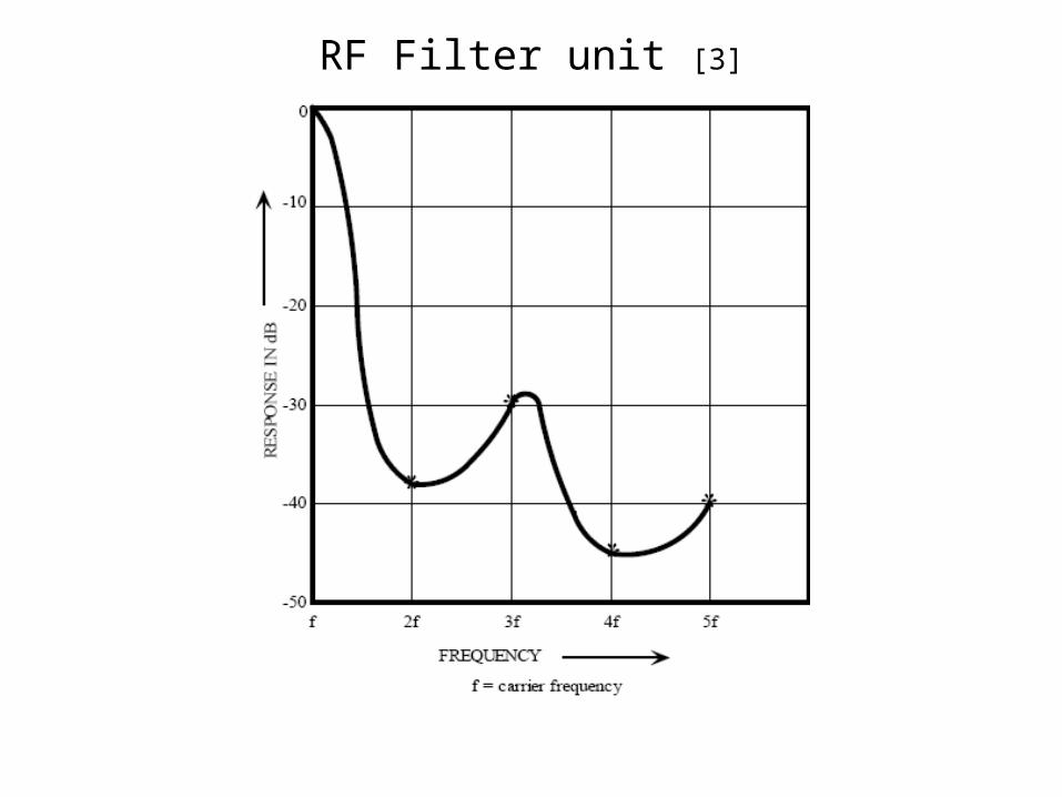
RF Filter unit [3]