Embed Size (px)
Citation preview

R Manohar Anaparthi Int. Journal of Engineering Research and Applications www.ijera.com
ISSN : 2248-9622, Vol. 4, Issue 12( Part 4), December 2014, pp.124-131
www.ijera.com 124 | P a g e
Pwm Control Strategy for Controlling Of Parallel Rectifiers In
Single Phase To Three Phase Drive System
Ramakrishna Manohar Anaparthi, S Rajasekhar Akula Sree Ramulu Institute of Engg & Technology Prathipadu, Tadepalligudem
ABSTRACT: This paper explains that how to develop and design, control of single phase to three phase drive system. The
proposed topology of drive system consisting of two parallel connected rectifiers, inverter and induction motor,
connected through inductor and capacitor, where used to produce balanced output to the motor drive. The main
objective of this proposed method is to reduce the circulating currents and harmonic distortions at the converter
input side, here the control strategy of drive system is PWM (pulse width modulations techniques) control
strategy, the proposed topology also provides fault compensation in the case of short circuit faults and failure of
switches for uninterrupted Power supplies. We also develop and simulate the MATLAB models for proposed
drive system, by using MATLAB/ Simulink the output results simulate and observed.
I. INTRODUCTION: Power electronics drives widely used in all most
all industries to drive different types of motors
specially induction motors. Power electronics
converters have been used to improve the power
Capability, reliability, efficiency, and Redundancy.
Electric utilities do not install three-phase power
as a matter of course because it cost significantly
more than single-phase installation. Hence we need to
conversion from single-phase to three-phase. Usually
the operation of converters in parallel requires a
transformer for isolation. However, weight, size, and
cost associated with the transformer may make such a
solution undesirable [1]. When an isolation
transformer is not used, the reduction of circulating
currents among different converter stages is an
important objective in the system design
Fig. 1. Conventional single-phase to three-phase drive
system
A single-phase to three-phase drive system
composed of two parallel single-phase rectifiers and a
three-phase inverter is proposed. The proposed
system is conceived to operate where the single-phase
utility grid is the unique option available. Compared
to the conventional topology, the proposed system
permits: to reduce the rectifier switch currents; the
total harmonic distortion (THD) of the grid current
with same switching frequency or the switching
frequency with same THD of the grid current; and to
increase the fault tolerance characteristics. In
addition, the losses of the proposed system may be
lower than that of the conventional counterpart. The
aforementioned benefits justify the initial investment
of the proposed system, due to the increase of number
of switches.
Fig 2 Modified (proposed) single-phase to 3-phase
drive topology
II. SYSTEM MODEL: The system is composed of grid, input inductors
(𝐿𝑎 ,𝐿′𝑎 ,𝐿𝑏 , and𝐿′𝑏 .), rectifiers (A and B), capacitor
bank at the dc link, inverter, and induction machine.
Rectifiers A and B are constituted of switches
𝑞𝑎1 , 𝑞 𝑎1 , 𝑞𝑎2and𝑞 𝑎2and𝑞𝑏1 , 𝑞 𝑏1,𝑞𝑏2
and𝑞 𝑏2respectively. The inverter is constituted of
switches𝑞 𝑠1 , 𝑞𝑠2,𝑞 𝑠2,𝑞𝑠3 and𝑞 𝑠3 . The conduction state
of the switches is represented by variable𝑠𝑞𝑎1 , 𝑠𝑞𝑠3,
where 𝑠𝑞= 1 indicates a closed switch while 𝑠𝑞= 0 an
open one.
From Fig. 2, the following equations can be derived
for the front-end rectifier
RESEARCH ARTICLE OPEN ACCESS

R Manohar Anaparthi Int. Journal of Engineering Research and Applications www.ijera.com
ISSN : 2248-9622, Vol. 4, Issue 12( Part 4), December 2014, pp.124-131
www.ijera.com 125 | P a g e
𝑣𝑎10 − 𝑣𝑎20 = 𝑒𝑔 − 𝑟𝑎 + 𝑙𝑎𝑝 𝑖𝑎 − (𝑟′𝑎 + 𝑙′ 𝑎𝑝)𝑖′𝑎 (1)
𝑣𝑏10 − 𝑣𝑏20 = 𝑒𝑔 − 𝑟𝑏 + 𝑙𝑏𝑝 𝑖𝑏 − (𝑟′𝑏 + 𝑙′ 𝑏𝑝)𝑖′𝑏 (2)
𝑣𝑎10 − 𝑣𝑏10 = 𝑟𝑏 + 𝑙𝑏𝑝 𝑖𝑏 − (𝑟𝑎 + 𝑙𝑎𝑝)𝑖𝑎 (3)
𝑣𝑎20 − 𝑣𝑏20 = 𝑟′𝑎 + 𝑙′𝑎𝑝 𝑖′𝑎 − 𝑟′𝑏 + 𝑙′ 𝑏𝑝 𝑖 ′ 𝑏 (4)
𝑖𝑔=𝑖𝑎 + 𝑖𝑏 = 𝑖′𝑎 + 𝑖′𝑏 (5)
Where p = d/dt and symbols like r and l represent
the resistances and inductances of the input inductors
La, L'a,𝑖𝑏 , and 𝐿′𝑏The circulating current io can be
defined from 𝑖𝑎and 𝑖′𝑎or 𝑖𝑏and i.e.
𝑖0=𝑖𝑎 − 𝑖′𝑎 = −𝑖𝑏 + 𝑖′𝑏 (6)
Introducing 𝑖𝑜and adding (3) and (4), Relations (1)—
(4) become
𝑣𝑎 = 𝑒𝑔 − 𝑟𝑎 + 𝑟′𝑎 + (𝑙𝑎 + 𝑙′𝑎 )𝑝 𝑖𝑎 + (𝑟′𝑎 + 𝑝)𝑖𝑜 (7)
𝑣𝑏 = 𝑒𝑔 − 𝑟𝑏 + 𝑟′𝑏 + (𝑙𝑏 + 𝑙′𝑏 )𝑝 𝑖𝑏 − 𝑟′𝑏 + 𝑙′
𝑏𝑝 𝑖𝑜 (8)
𝑣𝑜 = − 𝑟′𝑎 + 𝑟′
𝑏 + 𝑙′𝑎 + 𝑙′
𝑏 𝑝 𝑖𝑜 − 𝑟𝑎 − 𝑟′𝑎 +
𝑙𝑎−𝑙′𝑎𝑝𝑖𝑎+𝑟𝑏−𝑟′𝑏+𝑙𝑏−𝑙′𝑏𝑝𝑖𝑏 (9)
Where
𝑣𝑎 = 𝑣𝑎10 − 𝑣𝑎20 (10)
𝑣𝑏 = 𝑣𝑏10 − 𝑣𝑏20 (11)
𝑣𝑜 = 𝑣𝑎10 + 𝑣𝑎20 − 𝑣𝑏10 − 𝑣𝑏20 (12)
Relations (7)—(9) and (5) constitute the front-end
rectifier dynamic model. Therefore, 𝑣𝑎 (rectifier A), 𝑣𝑏
(rectifier B), and 𝑣𝑜 (rectifiers A and B) are used to
regulate currents𝑖𝑎 ,𝑖𝑏 , and𝑖𝑜 , respectively. Reference
currents 𝑖𝑎∗ and 𝑖𝑏
∗ are chosen equal to 𝑖𝑔∗ /2 and the
reference circulating current 𝑖𝑜∗is chosen equal to 0.In
order to both facilitate the control and share equally
current, voltage, and power between the rectifiers, the
four inductors should be equal, i.e., 𝑟′𝑔=𝑟𝑎 = 𝑟′𝑎 =
𝑟𝑏 = 𝑟′𝑏 and 𝑙′𝑔 = 𝑙𝑎= 𝑙′𝑎 =𝑙𝑏=𝑙′𝑏 . In this case, the
model (7)—(9) can be simplified to the model given by
𝑣𝑎 +𝑣0
2= 𝑒𝑔 − 2(𝑟′𝑔 + 𝑙′𝑔𝑝)𝑖𝑎 (13)
𝑣𝑏 −𝑣0
2= 𝑒𝑔 − 2(𝑟′𝑔 + 𝑙′𝑔𝑝)𝑖𝑏 (14)
𝑣𝑜 = −2(𝑟′𝑔 + 𝑙′𝑔𝑝)𝑖𝑜 (15)
Additionally, the equations for 𝑖𝑔 , 𝑖′𝑎 , 𝑖′𝑏 can be
written as
𝑣𝑎𝑏 =𝑣𝑎 +𝑣𝑏
2= 𝑒𝑔 − (𝑟′𝑔 + 𝑙′𝑔𝑝)𝑖𝑔 (16)
𝑣𝑎 −𝑣𝑜
2= 𝑒𝑔 − 2(𝑟′𝑔 + 𝑙′𝑔𝑝)𝑖′𝑎 (17)
𝑣𝑏 +𝑣𝑜
2= 𝑒𝑔 − 2(𝑟′𝑔 + 𝑙′𝑔𝑝)𝑖′𝑏 (18)
In this ideal case (four identical inductors), the
circulating current can be reduced to zero imposing
𝑣𝑜 = 𝑣𝑎10 + 𝑣𝑎20 − 𝑣𝑏10 − 𝑣𝑏20 = 0 (19)
When 𝑖𝑜 = 0(𝑖𝑎 = 𝑖′𝑎 , 𝑖𝑏 = 𝑖′𝑏 ) the system model
(7)-(9) is reduced to
𝑣𝑎 = 𝑒𝑔 − 2(𝑟′𝑔 + 𝑙′𝑔𝑝)𝑖𝑎 (20)
𝑣𝑏 = 𝑒𝑔 − 2(𝑟′𝑔 + 𝑙′𝑔𝑝)𝑖𝑏 . (21)
Then, the model of the proposed system
becomes similar to that of a system composed of two
conventional independent rectifiers.
IV. PWM STRATERGY: Considering that 𝑣𝑎
∗, 𝑣𝑏∗, and 𝑣𝑜
∗ denote the
reference voltages determined by the current
controllers. i.e.
𝑣𝑎∗ = 𝑣𝑎10
∗ − 𝑣𝑎20∗ , (22)
𝑣𝑏∗ = 𝑣𝑏10
∗ − 𝑣𝑏20∗ , (23)
𝑣𝑜∗ = 𝑣𝑎10
∗ + 𝑣𝑎20∗ − 𝑣𝑏10
∗ − 𝑣𝑏20∗ , (24)
The gating signals are directly calculated from the
reference pole voltages 𝑣𝑎10∗ , 𝑣𝑎20
∗ , 𝑣𝑏10∗ , 𝑣𝑏20
∗
Introducing an auxiliary variable 𝑣𝑥∗ = 𝑣𝑎20
∗ and
solving this system of equations,
𝑣𝑎10∗ = 𝑣𝑎
∗ + 𝑣𝑥∗ (25)
𝑣𝑎20∗ = 𝑣𝑥
∗ (26)
𝑣𝑏10∗ =
𝑣𝑎∗
2+
𝑣𝑏∗
2−
𝑣𝑜∗
2+ 𝑣𝑥
∗ (27)
𝑣𝑏20∗ =
𝑣𝑎∗
2−
𝑣𝑏∗
2−
𝑣𝑜∗
2+ 𝑣𝑥
∗ (28)
From these equations, it can be seen that,
besides𝑣𝑎∗,𝑣𝑏
∗ and 𝑣𝑜∗, the pole voltages depend on also
of 𝑣𝑥∗. The limit values of the variable 𝑣𝑥
∗can be
calculated by taking into account the maximum 𝑣𝑐∗/2
and minimum −𝑣𝑐∗/2 value of the pole voltages

R Manohar Anaparthi Int. Journal of Engineering Research and Applications www.ijera.com
ISSN : 2248-9622, Vol. 4, Issue 12( Part 4), December 2014, pp.124-131
www.ijera.com 126 | P a g e
𝑣𝑥 𝑚𝑎𝑥∗ = (𝑣𝑐
∗/2) – 𝑣𝑚𝑎𝑥∗ (29)
𝑣𝑥𝑚𝑖𝑛∗ = (-𝑣𝑐
∗/2) – 𝑣𝑚𝑖𝑛∗ (30)
Introducing a parameter μ (0 ≤ μ ≤ 1), the variable 𝑣𝑥∗
can be written as,
𝑣𝑥∗ = μ𝑣𝑥𝑚𝑎𝑥
∗ + (1- μ) 𝑣𝑥𝑚𝑖𝑛∗ (31)
Once 𝑣𝑥∗ is chosen, pole voltages𝑣𝑎10
∗ ,𝑣𝑎20∗ , 𝑣𝑏10
∗
and 𝑣𝑏20∗ are defined from (4) to (7).The parameter μ
changes the place of the voltage pulses related to 𝑣𝑎
and 𝑣𝑏 . And also μ influences the harmonic distortion
of the voltages generated by the rectifier.
SYSTEM CONTROL:
The gating signals are obtained by comparing pole
voltages with one (vt1), two (vt1 and vt2) or more
high-frequency triangular carrier signals [17]–[20]. In
the case of double-carrier approach, the phase shift of
the two triangular carrier signals (vt1 and vt2) is 1800.
The parameter μ changes the place of
the voltage pulses related to 𝑣𝑎and𝑣𝑏 . When 𝑣𝑥∗ =
𝑣𝑥𝑚𝑖𝑛∗ (μ = 0) or 𝑣𝑥
∗ = 𝑣𝑥𝑚𝑎𝑥∗ (μ = 1) are selected, the
pulses are placed in the starting or in the ending of
half period (Ts) of the triangular carrier signal.
Fig. 3. Control block diagram.
The control block diagram of Fig3,
highlighting the control of the rectifier. To
control the dc-link voltage and to guarantee the
grid power factor close to one. Additionally, the
circulating current 𝑖𝑜 in the rectifier of the
proposed system needs to be controlled. In this
way, the dc-link voltage 𝑣𝑐 is adjusted to its
reference value 𝑣𝑐∗ using the controller𝑅𝑐 , which
is a standard PI type controller. This controller
provides the amplitude of the reference grid
current Ig*. To control power factor and
harmonics in the grid side, the instantaneous
reference current Ig* must be synchronized with
voltage𝑒𝑔 , as given in the voltage-oriented
control (VOC) for three-phase system. This is
obtained via blocks 𝐺𝑒-𝑖𝑔 , based on a PLL
scheme. The reference currents 𝑖𝑎∗and𝑖𝑏
∗ are
obtained by making 𝑖𝑎∗ = 𝑖𝑏
∗ = 𝐼𝑔∗/2, which means
that each rectifier receives half of the grid
current. The control of the rectifier currents is
implemented using the controllers indicated by
blocks 𝑅𝑎and𝑅𝑏 . These current controllers
define the input reference voltages 𝑣𝑎∗and𝑣𝑏
∗.The
homopolar current is measured (𝑖𝑜 ) and
compared to its reference (𝑖𝑜∗ = 0). The error is
the input of PI controller Ro that determines the
voltage𝑣𝑜∗. The motor there-phase voltages are
supplied from the inverter (VSI). Block VSI-Ctr
indicates the inverter and its control. The control
system is composed of the PWM command and
a torque/flux control strategy (e.g., field-oriented
control or volts/hertz control).
COMPARISION OF THD’S:
Topology (PWM) THDp/THDc
Proposed (S-Ca μ = 0.5) 0.035
Proposed (D-Ca μ = 0.5) 0.041
Proposed (D-Ca μ = 0) 0.012
The dc-link capacitor current behavior is
examined in this section. The proposed converter
using double-carrier with μ = 0 provides the best
reduction of the high frequency harmonics. The
highest reduction of THD is obtained for the
converter using double-carrier with μ = 0 and the
THD obtained for μ = 1 is equal to that for μ = 0. By
observing the above table we can say that the
proposed method has lesser THD, when compared to
conventional one .And also from the above table it is
said that the THD of proposed one is lesser at double
carrier μ=0,when compared to single carrier μ=0.5
and double carrier μ=0.5. VI. COMPENSATION OF FAULT:

R Manohar Anaparthi Int. Journal of Engineering Research and Applications www.ijera.com
ISSN : 2248-9622, Vol. 4, Issue 12( Part 4), December 2014, pp.124-131
www.ijera.com 127 | P a g e
Fig. 4. Proposed configuration highlighting
devices of fault tolerant system
The fault compensation is achieved by
reconfiguring the power converter topology with the
help of isolating devices (fast active fuses—Fj , j = 1,
. . . , 7) and connecting devices (back-to-back
connected SCRs—t1 , t2 , t3 ), as observed in Fig. 4
and discussed in [21]–[24]. These devices are used to
redefine the post-fault converter topology, which
allows continuous operation of the drive after
isolation of the faulty power switches in the
converter. Fig. 5 presents the block diagram of the
fault diagnosis system. In this figure, the block fault
identification system (FIS) detects and locates the
faulty switches, defining the leg to be isolated. This
control system is based on the analysis of the pole
voltage error.
Fig.5. Block diagram of the fault diagnosis system
The proposed system can provide compensation
for open-circuit and short-circuit failures occurring in
the rectifier or inverter converter devices
The fault detection and identification is carried out in
four steps:
1) Measurement of pole voltages (vj 0);
2) Computation of the voltage error εj 0 by
comparison of reference voltages and
measurements affected in Step 1,
3) Determination as to whether these errors
correspond or not to a faulty condition; this can
be implemented by the hysteresis detector
shown in Fig. 5,
4) Identification of the faulty switches by using
ε₃j 0
This way, four possibilities of configurations have
been considered in terms of faults:
1) Pre-fault (―healthy‖) operation [see Fig. 6(a)];
2) Post-fault operation with fault at the rectifier B
[see Fig. 6(b)];
3) Post-fault operation with fault at the rectifier A
[see Fig. 6(c)];
4) Post-fault operation with fault at the inverter
[see Fig. 6(d)].
5) When the fault occurrence is detected and
identified by the control system, the proposed
system is reconfigured and becomes similar to
that in Fig. 1.
Fig. 6. Possibilities of configurations in terms of fault
occurrence. (a) Pre-fault system. (b) Post-fault system
with fault at the rectifier B. (c) Post-fault system with
fault at the rectifier A. (d) Post-fault system with fault
at the inverter.
VII. EFFICIENCY TABLE:
By observing the above table we can conclude that
the efficiency of proposed system has better at D-Ca
μ = 0 as compared with the conventional system at
the same operating conditions. The initial investment
of The proposed system is higher than that of the
standard one, since the number of switches and de-
vices such as fuses and triacs is highest. But,
considering the scenario when faults may occur, the
drive operation needs to be stopped for a
nonprogrammer maintenance schedule. The cost of
this schedule can be high and this justifies the high
initial investment inherent of fault-tolerant motor
drive systems. On the other hand, the initial
investment can be justified if the THD of the
conventional system is a critical factor.
VIII. SIMULATION RESULTS: The proposed drive system is implemented by
using MAT LAB SIMULINK TOOLS by connecting
of blocks from mat lab library
𝛈𝒑
𝛈𝒄
− 𝟏
Frequency/Inductor S-Ca μ =
0.5
D-Ca μ
= 0.5
D-Ca μ
= 0
5 kHz/ (L’g = Lg) -0.75% -0.29% 1.61%

R Manohar Anaparthi Int. Journal of Engineering Research and Applications www.ijera.com
ISSN : 2248-9622, Vol. 4, Issue 12( Part 4), December 2014, pp.124-131
www.ijera.com 128 | P a g e
Fig.7: Mat lab model of proposed drive system
The steady-state experimental results are shown.
The waveforms in this figure are:8(a) voltage and
current of the grid,8(b) dc-link voltage,8(c) currents
of rectifier A and circulating current, 8.(d) currents of
rectifiers A and B, and8.(e) load line voltage. Note
that, with the proposed configuration, all control
demanded for single-phase to three-phase converter
has been established. The control guarantees
sinusoidal grid current with power factor close to
one [see Fig.8.(a)], dc-link and machine voltages
under control [see Fig.8.(b) and8. (e)]. Furthermore,
the proposed configuration provides current reduction in
the rectifier side (half of the current of the standard
topology) [see Fig. 8.(d)], which can provide loss
reduction. Also, the control guarantees the circulating
current close to zero [see Fig. 8. (c)].The same set of
experimental results was obtained for transient in
the machine voltages, as observed in Fig. 9.(a) A
volts/hertz control was applied for the three-phase
machine, from V/Hz = 83.3 V/40 Hz to V/Hz = 125
V/60 Hz [see Fig. 9.(e)], which implies in increased
of power furnished by
8. 𝑎 . Grid voltage 𝑣𝑔 , gird current 𝑖𝑔
8. (b) dc-link voltage 𝑣𝑐
8.(c) Currents of rectifier A (𝑖𝑎 , 𝑖′𝑎 ) and circulating
current (𝑖0).
8. (d) Currents of rectifiers A (𝑖𝑎 ) and B (𝑖𝑏)
8. (e) load line voltage
The below waveforms are Experimental results for a
volts/hertz transient applied to the three phase
motor. 9.(a) Grid voltage eg and gird current
ig,9.(b)Capacitor
R Manohar Anaparthi Int. Journal of Engineering Research and Applications www.ijera.com
ISSN : 2248-9622, Vol. 4, Issue 12( Part 4), December 2014, pp.124-131
www.ijera.com 129 | P a g e
voltage(vc),9.(c) Currents of rectifier A and
circulating current(io),9.(d)Currents of rectifiers
A(ia) and B(ib),9.(e)Line voltage of the load.
9. 𝑎 . Grid voltage 𝑣𝑔 , gird current 𝑖𝑔
9. (b) dc-link voltage 𝑣𝑐
9. (c) Currents of rectifier A (𝑖𝑎 , 𝑖′𝑎 ) and circulating
current (𝑖0).
9.(d) Currents of rectifiers A (𝑖𝑎 ) and B (𝑖𝑏)
9. (e) load line voltage
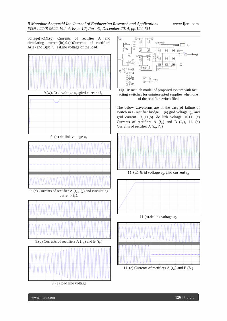
Fig 10: mat lab model of proposed system with fast
acting switches for uninterrupted supplies when one
of the rectifier switch filed
The below waveforms are in the case of failure of
switch in B rectifier bridge 11(a).grid voltage 𝑣𝑔 , and
grid current 𝑖𝑔 ,11(b). dc link voltage, 𝑣𝑐11. (c)
Currents of rectifiers A (𝑖𝑎 ) and B (𝑖𝑏 ), 11. (d)
Currents of rectifier A (𝑖𝑎 , 𝑖′𝑎 )
11. 𝑎 . Grid voltage 𝑣𝑔 , gird current 𝑖𝑔
11.(b).dc link voltage 𝑣𝑐
11. (c) Currents of rectifiers A (𝑖𝑎 ) and B (𝑖𝑏)

R Manohar Anaparthi Int. Journal of Engineering Research and Applications www.ijera.com
ISSN : 2248-9622, Vol. 4, Issue 12( Part 4), December 2014, pp.124-131
www.ijera.com 130 | P a g e
11. (d) Currents of rectifier A (𝑖𝑎 , 𝑖′𝑎 )
Simulation result highlighting the interleaved
operation
Conclusion: A single phase to three phase drive system
combines two parallel rectifiers without the use of
transformers. The system model and the control
strategy, including the PWM technique, have been
developed. The complete comparison between the
proposed and standard configurations has been
carried out. Compared to the conventional topology,
the proposed system permits to reduce the rectifier
switch currents, the THD of the grid current and to
increase the fault tolerance characteristics. The
simulation results have shown that the system is con-
trolled properly, even with transient and occurrence
of faults.
Reference: [1] J.-K. Park, J.-M. Kwon, E.-H. Kim, and B.H.
Kwon, ―High-performance transformer less
online UPS,‖ IEEE Trans. Ind. Electron.,
vol. 55, no. 8, 2943–2953, Aug. 2008.
[2] Z. Ye, D. Boroyevich, J.-Y. Choi, and F. C.
Lee, ―Control of circulating current in two
parallel three-phase boost rectifiers,‖ IEEE
Trans. Power Electron., vol. 17, no. 5, pp.
609–615, Sep. 2002.
[3] S. K. Mazumder, ―Continuous and discrete
variable-structure controls for parallel three
phase boost rectifier,‖ IEEE Trans. Ind.
Electron., vol. 52, no. 2, pp. 340–354, Apr.
2005
[4] X. Sun, L.-K. Wong, Y.-S. Lee, and D. Xu,
―Design and analysis of an optimal controller
for parallel multi inverter systems,‖
IEEE Trans. Circuits Syst. II, vol. 53, no. 1,
pp. 56– 61, Jan. 2006.
[5] Z. Ye, P. Jain, and P. Sen, ―Circulating
current minimization in high-frequency AC
power distribution architecture with
multiple inverter modules operated in
parallel,‖ IEEE Trans. Ind. Electron., vol. 54,
no. 5, 2673–2687, Oct. 2007
[6] P.-T. Cheng, C.-C. Hou, and J.-S. Li, ―Design
of an auxiliary converter for the diode
rectifier and the analysis of the circulating
current,‖ IEEE Trans. Power Electron., vol.
23, no. 4, pp. 1658–1667, Jul. 2008.
[7] H. Cai, R. Zhao, and H. Yang, ―Study on
ideal operation status of parallel inverters,‖
IEEE Trans. Power Electron., vol. 23, no. 6,
pp. 2964–2969, Nov. 2008.
[8] P. Enjeti and A. Rahman, ―A new single
phase to three phase converter with active
input current shaping for low cost AC motor
drives,‖ IEEE Trans. Ind. Appl., vol. 29, no.
2, pp. 806813, Jul./Aug. 1993.
[9] J. Itoh and K. Fujita, ―Novel unity power
factor circuits using zero-vector control for
single phase input systems,‖ IEEE Trans.
Power Electron., vol. 15, no. 1, pp. 36–43,
Jan. 2000.
[10] B. K. Lee, B. Fahimi, and M. Ehsani,
―Overview of reduced parts converter
topologies for AC motor drives,‖ in Proc.
IEEE PESC, 2001, pp. 2019– 2024
[11] C. B. Jacobina, M. B. de R. Correa, A. M. N.
Lima, and E. R. C. da Silva, ―AC motor drive
systems with a reduced switch count
converter,‖ IEEE Trans. Ind. Appl., vol. 39,
no. 5, pp. 1333–1342, Sep./Oct. 2003.
[12] R. Q. Machado, S. Buso, and J. A. Pomilio,
―A line-interactive single-phase to three-
phase converter system,‖ IEEE Trans. Power
Electron., vol. 21, no. 6, pp. 1628–1636, May
2006.
[13] O. Ojo, W. Zhiqiao, G. Dong, and S. Asuri,
―High-performance speed-sensor less control
of an induction motor drive using a
minimalist single-phase PWM converter,‖
IEEE Trans. Ind. Appl., vol. 41, no. 4, pp.
996– 1004, Jul./Aug. 2005.
[14] J. R. Rodr´ıguez, J. W. Dixon, J. R. Espinoza,
J. Pontt, and P. Lezana, ―PWM regenerative
rectifiers: State of the art,‖ IEEE Trans. Ind.
Electron., vol. 52, no. 1, pp. 5–22, Feb. 2005.
[15] M. N. Uddin, T. S. Radwan, and M. A.
Rahman, ―Fuzzy-logic-controller-based

R Manohar Anaparthi Int. Journal of Engineering Research and Applications www.ijera.com
ISSN : 2248-9622, Vol. 4, Issue 12( Part 4), December 2014, pp.124-131
www.ijera.com 131 | P a g e
costeffective four-switch three-phase inverter-
fed IPM synchronous motor drive system,‖
IEEE Trans. Ind. Appl., vol. 42, no. 1,21–30,
Jan./Feb. 2006
[16] D.-C. Lee and Y.-S. Kim, ―Control of single
phase-to-three-phase AC/DC/AC PWM
converters for induction motor drives,‖ IEEE
Trans. Ind. Electron., vol. 54, no. 2, pp.
797804, Apr. 2007.
[17] J. Holtz, ―Pulse width modulation for
electronic power conversion,‖ Proc. IEEE,
vol. 82, no. 8, pp. 1194–1214, Aug. 1994
[18] A. M. Trzynadlowski, R. L. Kirlin, and S. F.
Legowski, ―Space vector PWM technique
with minimum switching losses and a variable
pulse rate,‖ IEEE Trans. Ind. Electron., vol.
44, no. 2, pp. 173–181, Apr. 1997
[19] O. Ojo and P. M. Kshirsagar, ―Concise
modulation strategies for four-leg voltage
source inverters,‖ IEEE Trans. Power
Electron., vol. 19, no. 1, 46–53, Jan. 2004.
[20] C. B. Jacobina, A. M. N. Lima, E. R. C. da
Silva, R. N. C. Alves, and P. F. Seixas,
―Digital scalar pulse-width modulation: a
simple approach to introduce non-sinusoidal
modulating waveforms,‖ IEEE Trans. Power
Electron., vol. 16, no. 3, pp. 351359, May
2001.
[21] R. L. A. Ribeiro, C. B. Jacobina, E. R. C. da
Silva, and A. M. N. Lima, ―Fault detection of
open-switch damage in voltage-fed PWM
motor drive systems,‖ IEEE Trans. Power
Electron., vol. 18, no. 2, pp. 587–593, Apr.
2003.
[22] B. A. Welchko, T. A. Lipo, T. M. Jahns, and
S. E. Schulz, ―Fault tolerant three-phase AC
motor drive topologies: A comparison of
features, cost, and limitations,‖ IEEE Trans.
Power Electron., vol. 19, no. 4, pp. 1108–
1116, Jul. 2004.
[23] S. Kwak and H. Toliyat, ―An approach to
fault-tolerant three-phase matrix converter
drives,‖ IEEE Trans. Energy Converters., vol.
22, no. 4, pp. 855– 863, Dec. 2003.
[24] D. Campos-Delgado, D. Espinoza-Trejo, and
E Palacios, ―Fault-tolerant control in variable
speed drives: A survey,‖ IET Electr. Power
Appl., vol. 2, no. 2, pp. 121–134, Mar. 2008.