Embed Size (px)
Citation preview
DISCLAIMER : System Plus Consulting provides cost studies based on its knowledge of the manufacturing and selling prices of electronic components and systems. The given values are realistic estimates which do not bind System Plus Consulting nor the manufacturers quoted in the report. System Plus Consulting is in no case responsible for the consequences related to the use which is made of the contents of this report. The quoted trademarks are property of their owners.
© 2013 by SYSTEM PLUS CONSULTING, all rights reserved. 1
Electronic Costing & Technology Experts
www.systemplus.fr21 rue la Nouë Bras de Fer44200 Nantes – France Phone : +33 (0) 240 180 916 email : [email protected]
June 2013 – Version 1 – Written by Sylvain Hallereau
SORAA MR16-50-B01-12-830-25 - LED
Return to TOC
© 2013 by SYSTEM PLUS CONSULTING, all rights reserved. 2
Glossary1. Overview / Introduction 4
– Executive Summary
– Reverse Costing Methodology
2. Companies Profile 8– SORAA Profile
3. Lightchip Package and Tri-LED Characteristics 10– Lightchip Characteristics
4. Physical Analysis 14– Physical Analysis Methodology
– SORAA MR16 Lamp
– Lightchip Package Views & Dimensions
– Lightchip Package and the Flex
– Lightchip Package Opening
– Lightchip Package Cross-Section
– Phosphor
– Tri-LED Assembly
– Lightchip Package Characteristics
– Tri-LED Views & Dimensions
– Cathode
– Tri-LED Singulation
– Anode
– Epitaxy
– Tri-LED Thickness
– Tri-LED Characteristics
5. Manufacturing Process Flow 42– Global Overview
– Tri-LED Fabrication Unit
– Tri-LED Process Flow
– Lightchip Fabrication Unit
– Lightchip Process Flow
6. Cost Analysis 53– Synthesis of the cost analysis
– Main steps of economic analysis
– Yields Hypotheses
– GaN Substrate
– Epitaxy Step
– Tri-LED Front-End Cost
– Tri-LED Wafer Cost
– Tri-LED Cost per process steps
– Tri-LED Equipment Cost per Family
– Tri-LED Material Cost per Family
– Back-End : Probe and cleaving Cost
– Lightchip Packaging Cost
– Lightchip Wafer Cost
– Final Assembly Cost
– Component Cost & Price
Future 74
Contact 75
SORAA MR16-50-B01-12-830-25 - LED
Return to TOC
© 2013 by SYSTEM PLUS CONSULTING, all rights reserved. 3
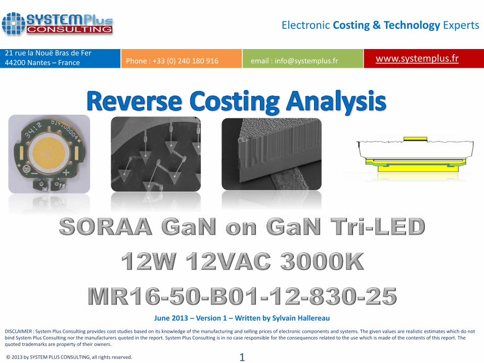
• This full Reverse Costing study has been conducted in order to give insight on technology data,manufacturing cost of the Light chip and the 36 Tri-LED in the MR16-50-B01-12-830-25 MR16 lampfrom SORAA. The tri-LED component is a LED in GaN on GaN . The Lightchip is a silicon based waferlevel packaging.
• The MR16-50-B01-12-830-25 lamp contains 36 Tri-LED dies. Each LED is triangular and measures0.07sq mm.
• We estimated that SORAA design and manufacture the GaN on GaN LED and the silicon based waferlevel package in their factories in California.
Tri-LED – Triangular LED (SORAA designation)
Lightchip – name of the silicon based wafer level packaging (SORAA designation)
SORAA MR16-50-B01-12-830-25 - LED
Return to TOC
© 2013 by SYSTEM PLUS CONSULTING, all rights reserved. 4
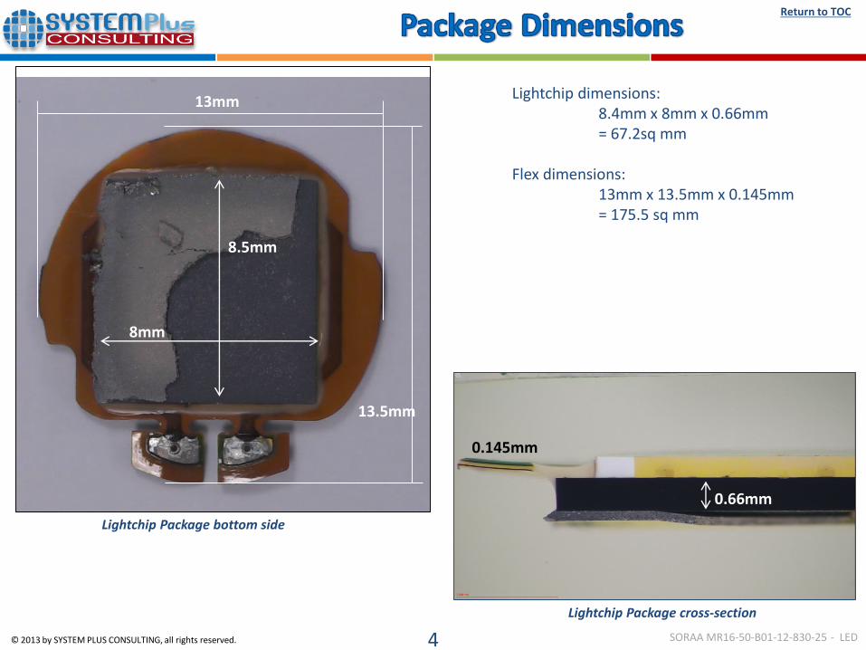
Lightchip Package cross-section
Lightchip Package bottom side
Lightchip dimensions:8.4mm x 8mm x 0.66mm= 67.2sq mm
Flex dimensions:13mm x 13.5mm x 0.145mm= 175.5 sq mm
13mm
13.5mm
8.5mm
8mm
0.66mm
0.145mm
SORAA MR16-50-B01-12-830-25 - LED
Return to TOC
© 2013 by SYSTEM PLUS CONSULTING, all rights reserved. 5
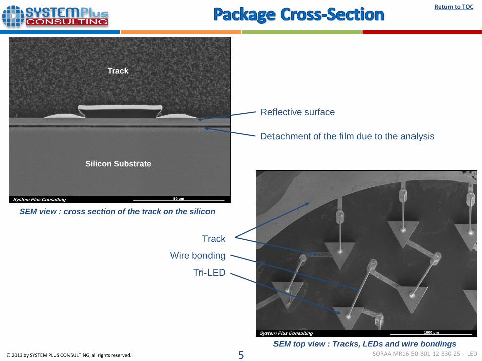
Track
Wire bonding
Tri-LED
Silicon Substrate
Detachment of the film due to the analysis
SEM view : cross section of the track on the silicon
Track
SEM top view : Tracks, LEDs and wire bondings
Reflective surface
SORAA MR16-50-B01-12-830-25 - LED
Return to TOC
© 2013 by SYSTEM PLUS CONSULTING, all rights reserved. 6
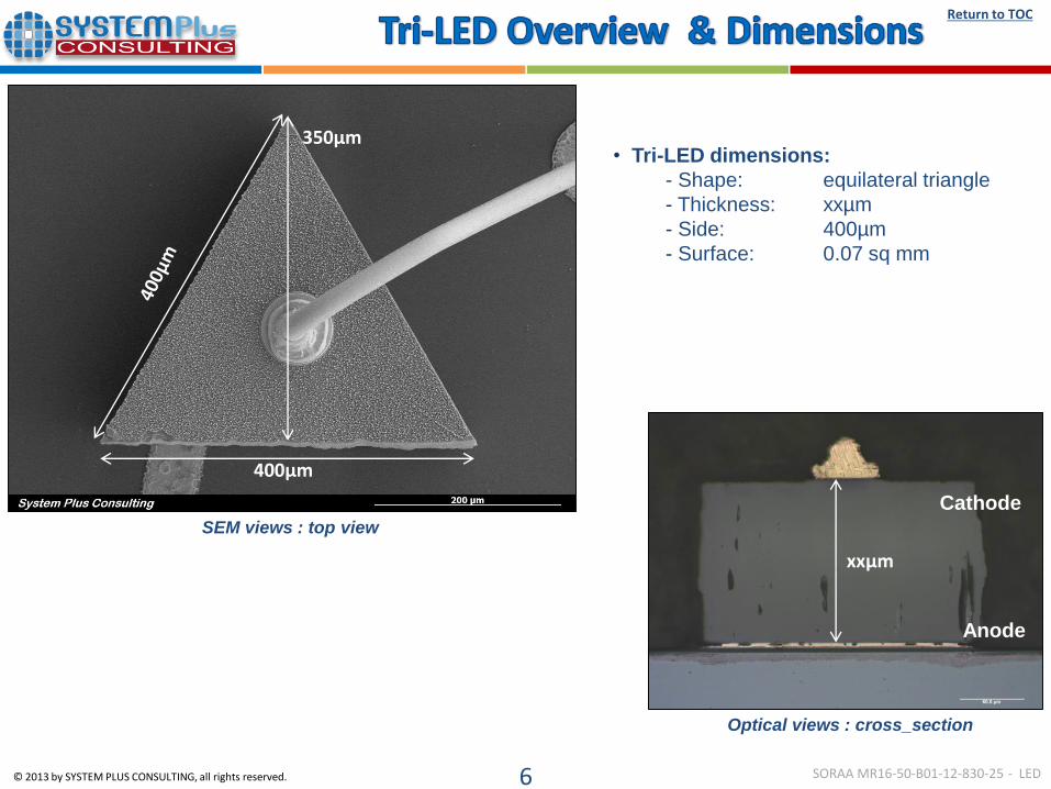
Optical views : cross_section
Cross-
Section
SEM views : top view
Cathode
Anode
• Tri-LED dimensions:
- Shape: equilateral triangle
- Thickness: xxµm
- Side: 400µm
- Surface: 0.07 sq mm
400µm
xxµm
350µm
SORAA MR16-50-B01-12-830-25 - LED
Return to TOC
© 2013 by SYSTEM PLUS CONSULTING, all rights reserved. 7
Optical view : cross-section die, edge of the
transistor.
Silicone
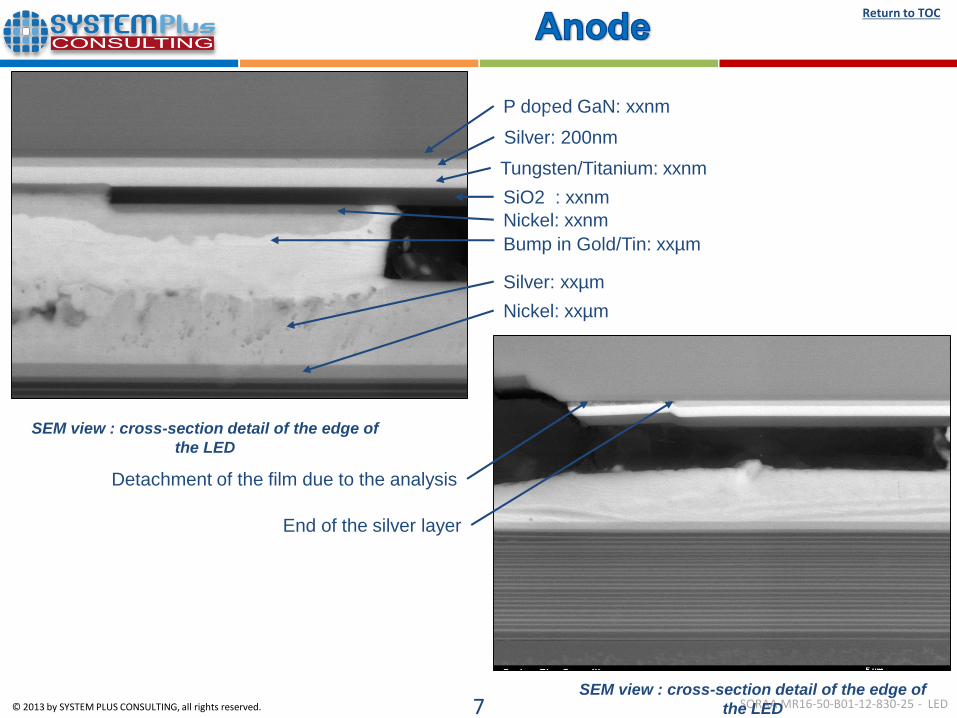
P doped GaN: xxnm
P layer
End of the silver layer
SEM view : cross-section detail of the edge of
the LED
1µm
Drift layer
SEM view : cross-section detail of the edge of
the LED
Silver: 200nm
Tungsten/Titanium: xxnm
SiO2 : xxnm
Nickel: xxnm
Bump in Gold/Tin: xxµm
Silver: xxµm
Nickel: xxµm
Detachment of the film due to the analysis
SORAA MR16-50-B01-12-830-25 - LED
Return to TOC
© 2013 by SYSTEM PLUS CONSULTING, all rights reserved. 8
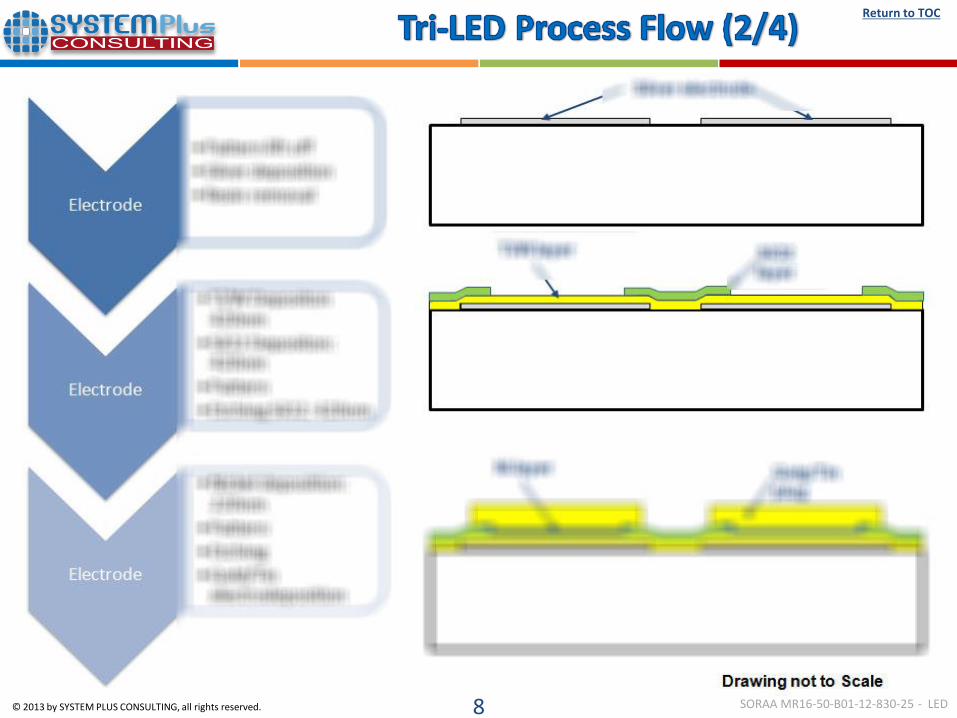
SORAA MR16-50-B01-12-830-25 - LED
Return to TOC
© 2013 by SYSTEM PLUS CONSULTING, all rights reserved. 9
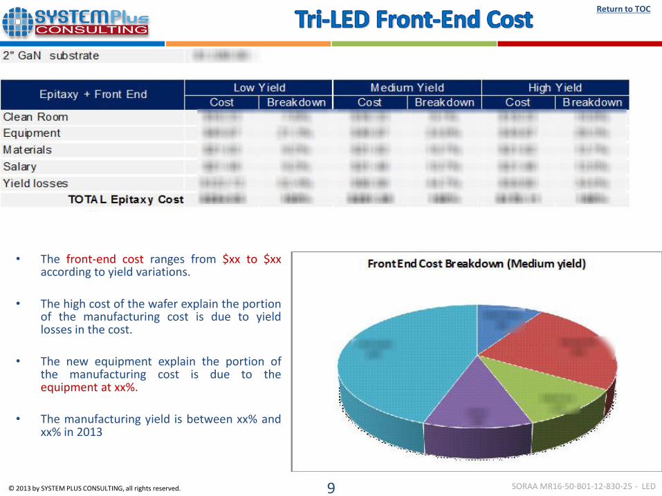
• The front-end cost ranges from $xx to $xxaccording to yield variations.
• The high cost of the wafer explain the portionof the manufacturing cost is due to yieldlosses in the cost.
• The new equipment explain the portion ofthe manufacturing cost is due to theequipment at xx%.
• The manufacturing yield is between xx% andxx% in 2013
SORAA MR16-50-B01-12-830-25 - LED
Return to TOC
© 2013 by SYSTEM PLUS CONSULTING, all rights reserved. 10

SORAA MR16-50-B01-12-830-25 - LED
Return to TOC
© 2013 by SYSTEM PLUS CONSULTING, all rights reserved. 11
• This reverse costing analysis represents the best cost/price evaluation given the
publically available data, completed with industry expert estimates.
• These results are open for discussion. We can re-evaluate this circuit with your
information. Please contact us:
Partner:
Le Quartz
75 cours Emile Zola
69100 Lyon-Villeurbanne
+33 (0)4 72 83 01 80
www.yole.fr