Embed Size (px)
Citation preview

Final Project Design of
EE577A VLSI System Design
Either static or dynamic logic-based implementation is acceptable;
All inputs, outputs and intermediate stage of the multiplier are registered with positive-edge triggered master-slave D-flip-flops;
No setup time and hold time violations; VDD=1.8V, 0.18μm technology; Transition times of primary inputs and clock
signal are 10ps; Clock signal has 50% duty ratio and infinite
driving ability
• Support multiple simple RISC instructions, such as Add, Multiply, Store and Load;
• 5-stage pipelined structure of CPU comprised of Decoding Logic, Register File, Execution Units, Memory and other peripheral circuitries;
• 8-bytes Register File supporting simultaneous read and write;
• 8-bit Adder;• two-stage pipelined 8-by-8 array multiplier;• SRAM-based 256-bit cache memory
supporting load word and store word
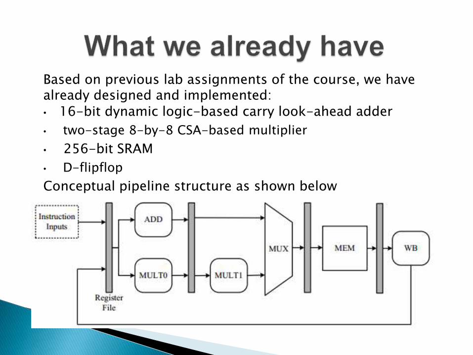
Based on previous lab assignments of the course, we have already designed and implemented:• 16-bit dynamic logic-based carry look-ahead adder
• two-stage 8-by-8 CSA-based multiplier
• 256-bit SRAM
• D-flipflop
Conceptual pipeline structure as shown below
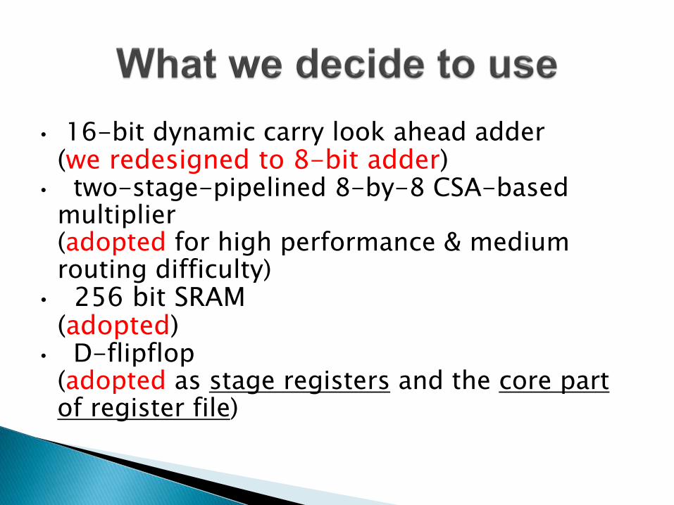
• 16-bit dynamic carry look ahead adder (we redesigned to 8-bit adder)
• two-stage-pipelined 8-by-8 CSA-based multiplier (adopted for high performance & medium routing difficulty)
• 256 bit SRAM (adopted)
• D-flipflop(adopted as stage registers and the core part of register file)
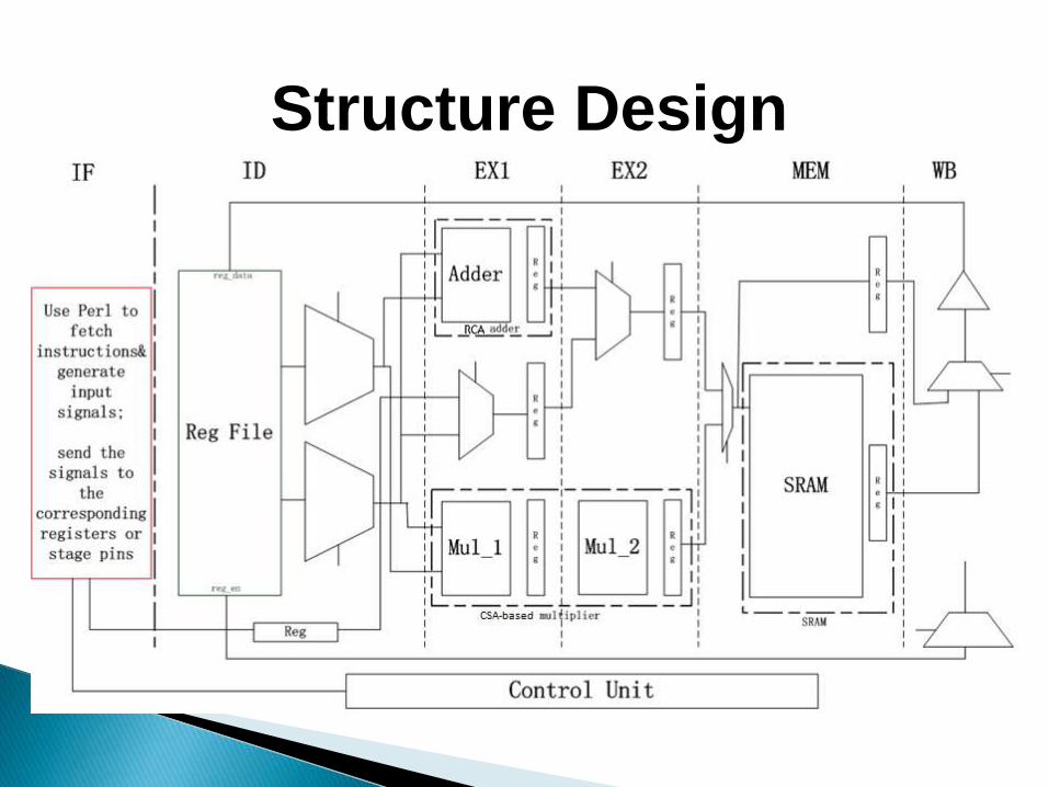
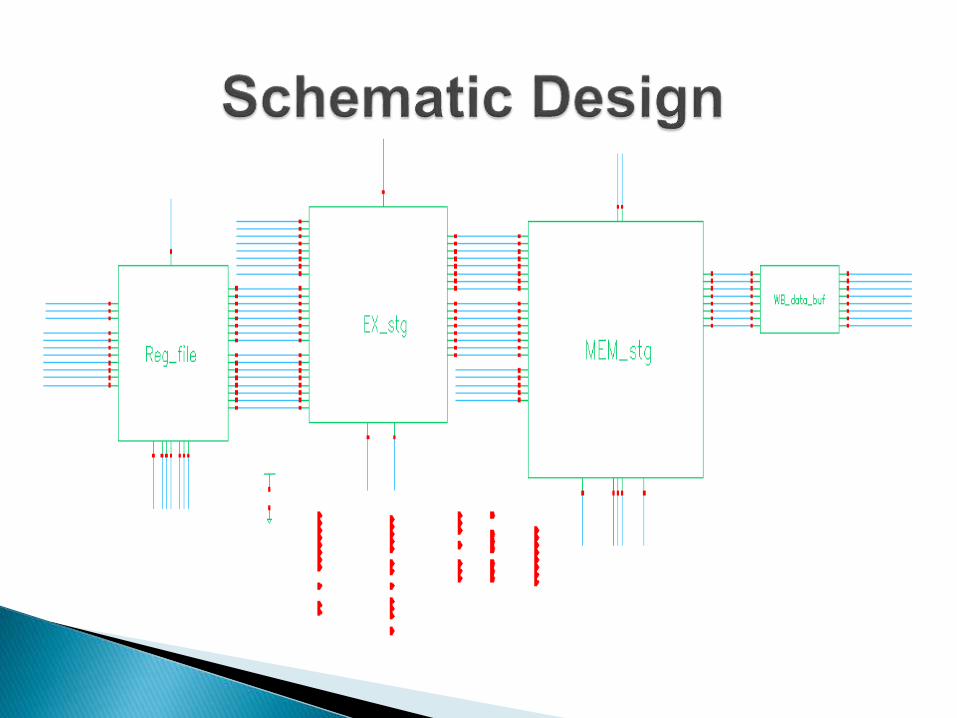
Structure Design

• Based on proper timing performance analysis, we add additional buffer to the clock signal of certain pipeline stages for time borrowing;
• Based on spice simulation results, it is desirable to perform time borrowing between ID stage and EX1 stage;
• We may use negative-edge-triggered DFF for Register File to save time in WB stage. However, it will not have significant benefit due to hold time violation;
Watch out for the input signals in MEM stage: some signals like pre-charge, read_en, write_en, etc., are not in full pulse form
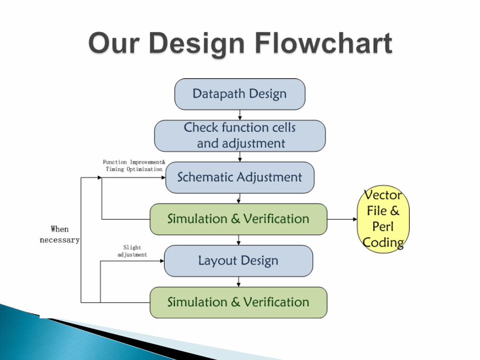
We have used perl programming to generate several proper vector files for extensive simulations
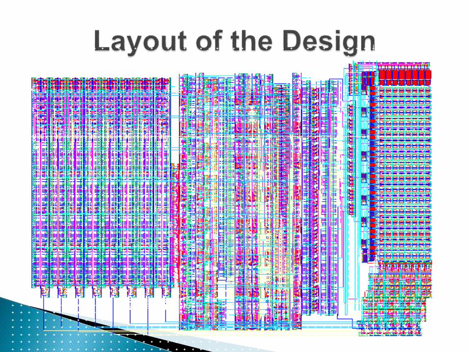
• Functional Clock Cycle: 3ns
• Layout Area: 240umx180um
To achieve better performance, we may want to make the delay of each stage more balanced with each other (further time borrowing can achieve this goal to some extent; however, glitches would increase power consumption); or further pipelining◦ Especially, we need to shorten the delay of the first stage of
the multiplier;
We may use gated-clock DFF array instead of the current mux-based DFF design (this will significant reduce the overall power consumption);
Also, better floorplan may reduce the delay in WB stage;
…

Thanks to our respected instructor Yanzhi Wang,
dearest TAs Di Zhu and Yu Cao
and Mentors Wentao Liu and Lin Zhou
Group Members: Xue Jiang, Chennan Li, Bojun Wang