Embed Size (px)
Citation preview

MODULE
SYSTEM
LOGIC GATE
CIRCUIT
D Q
CMOS Inverter
ASIC
Full-Custom
Semi-C
ustomPr
ogra
mm
able
FPGA
PLD
Cell-Based
Gate Arrays
General P
urpose
DRAM & SRAM
Microprocessor
ASSP
Controller Chip
Modem Chip
X
Combinational SequentialREG
MEM
OR
Y
DE
CO
DE
R
MUX
Simple
BasicFA
AB
Ci
S
Co
Complex
Static Dynamic
ParallelConnection
SeriesConnection
p n n+ +
MOSFETBipolar Diode
n pn+ n+p
DEVICE
WORLD O
F DIGITAL IC
Copy Right
August 2002Maitham Shams
Dept of Electronics
Carleton UniversityOttawa, CANADA
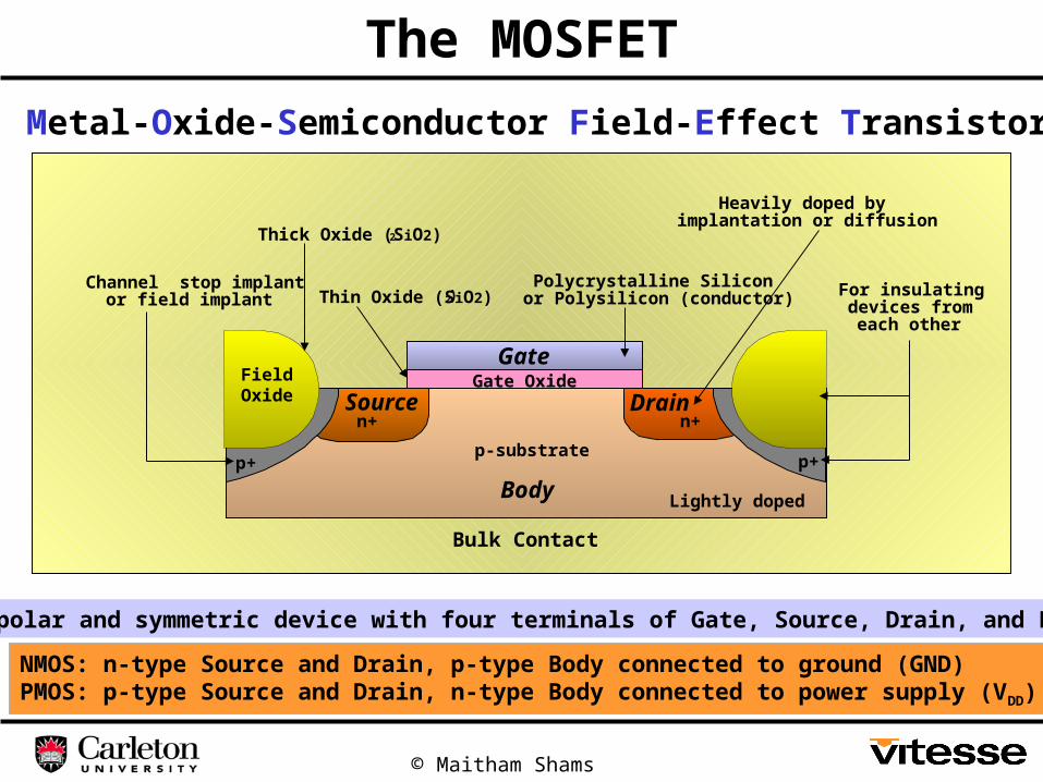
The MOSFET
© Maitham Shams 2002
n+ n+
Gate OxideSource Drain
Body
p-substrate
Gate
2Thin Oxide (SiO2))Polycrystalline Silicon
or Polysilicon (conductor)
Lightly doped
Bulk Contact
FieldOxide
p+ p+
Channel stop implantor field implant
2Thick Oxide (SiO2)
Heavily doped byimplantation or diffusion
For insulatingdevices fromeach other
Metal-Oxide-Semiconductor Field-Effect Transistor
Unipolar and symmetric device with four terminals of Gate, Source, Drain, and Body
NMOS: n-type Source and Drain, p-type Body connected to ground (GND)PMOS: p-type Source and Drain, n-type Body connected to power supply (VDD)
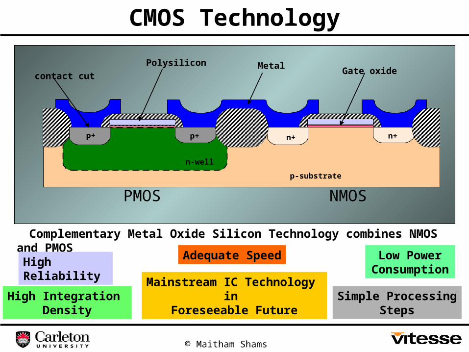
CMOS Technology
© Maitham Shams 2002
PMOS NMOS
p+ n+ n+
p-substrate
p+
contact cut
Polysilicon
n-well
MetalGate oxide
Complementary Metal Oxide Silicon Technology combines NMOS and PMOS
Mainstream IC Technology in
Foreseeable FutureHigh Integration
DensitySimple Processing
Steps
Low Power Consumption
Adequate SpeedHigh Reliability

MOSFET Types and Symbols
© Maitham Shams 2002
D
G
S
D
G
S
D
G
S
D
G
S
B
Analog Digital With non standard substrate connection
Enhancement PMOS Depletion PMOS
I DS
VGS +VTp
0
IDS
VGS -V Tp
0
D
G
S
D
G
S
D
G
S
B
D
G
S
Analog Digital With non standard substrate connection
Enhancement NMOS Depletion NMOS
I DS
VGS +VTn0
0
I DS
VGS -VTn
Enhancement mode transistors are normally OFF (non-conducting with zero bias)Depletion mode transistors are normally ON (conduct with zero bias)
Most CMOS ICs use Enhancement type MOS

© Maitham Shams 2002
AccumulationGate
Body
VGS +
-
n+ n+
Source Drain
p-type substrate
+_ +
_
+_ +
_
+_
+_
(B)
(S) (G) (D)
TGS VV 0
Depletion
Cut-off (no current)
TGS VV 0DSV
MOS Theory of Operation
G
Depletion layer
n+ n+
p-type substrate
_DS
B
__ _ __
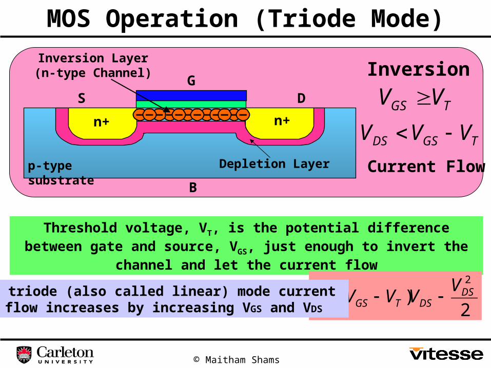
MOS Operation (Triode Mode)
© Maitham Shams 2002
Threshold voltage, VT, is the potential difference between gate and source, VGS, just enough to invert the channel and let the current flow
Inversion Layer(n-type Channel)
G
Depletion Layer
n+ n+
p-type substrate
DS_
B
___ _ __ _ _ __ _
Inversion
TGS VV
TGSDS VVV
2)(
2DS
DSTGS
VVVVI
Current Flow
In triode (also called linear) mode current flow increases by increasing VGS and VDS
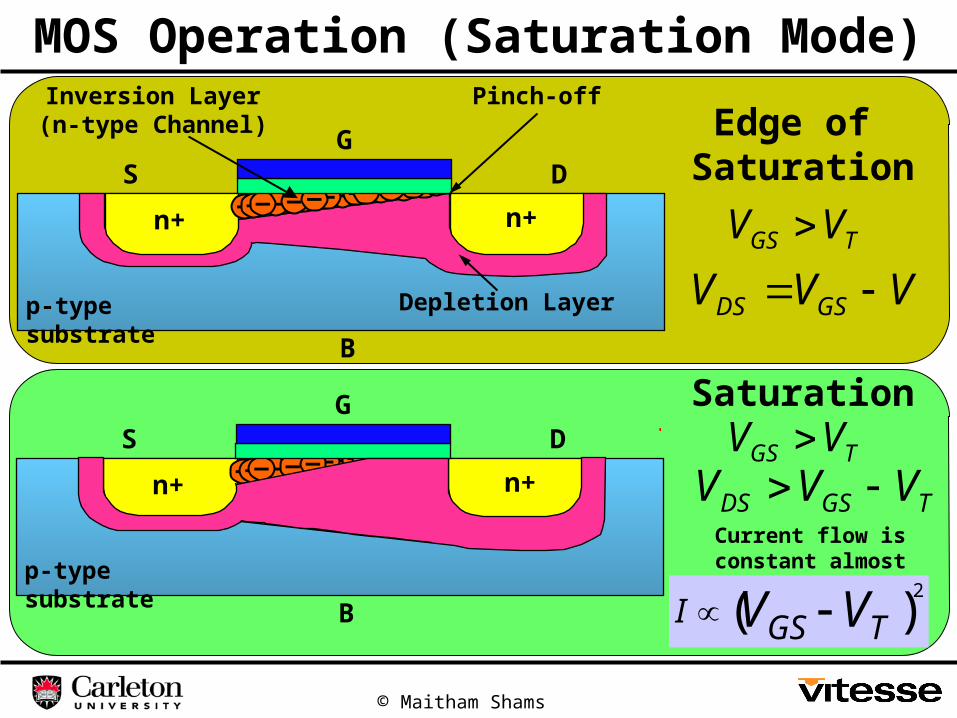
MOS Operation (Saturation Mode)
© Maitham Shams 2002
Current flow is constant almost independent of VDS
Inversion Layer(n-type Channel)
Pinch-off
G
Depletion Layer
n+ n+
p-type substrate
DS_
B
___ _____ _ _ _ _ __ __ _
G
n+ n+
p-type substrate
DS_
B
___ _____ _ _ _ _ __ __ _
Edge of Saturation
TGS VV
VVV GSDS
TGS VV TGSDS VVV
Saturation
)(2
TGSI VV
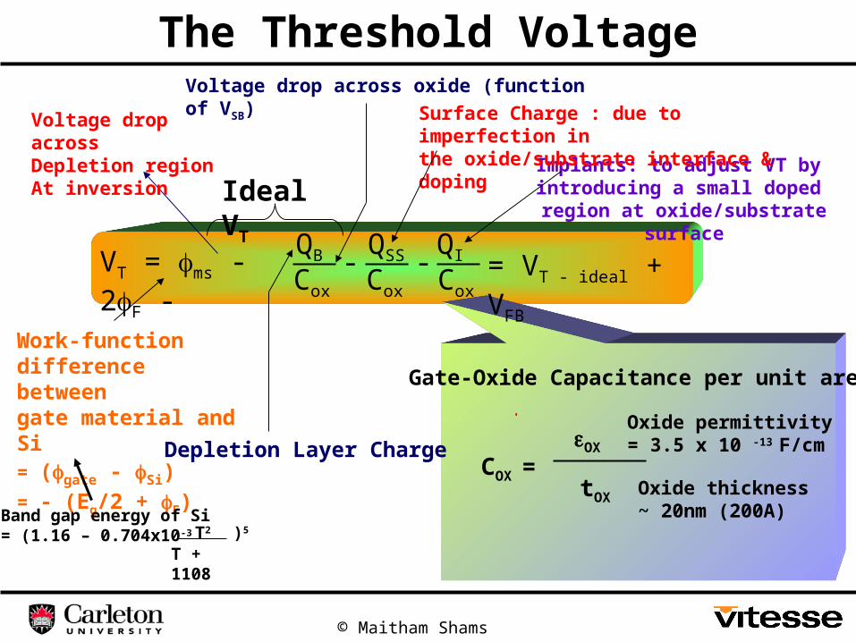
The Threshold Voltage
© Maitham Shams 2002
VT = ms - 2F -QB
Cox
-QSS
Cox
-QI
Cox= VT - ideal + VFB
Work-functiondifference betweengate material and Si = (gate - Si)
= - (Eg/2 + F)
Ideal VT
Voltage drop acrossDepletion regionAt inversion
Voltage drop across oxide (function of VSB)
Implants: to adjust VT by introducing a small doped
region at oxide/substrate surface
Surface Charge : due to imperfection in the oxide/substrate interface & doping
Depletion Layer Charge
Band gap energy of Si= (1.16 – 0.704x10⁻³ T2
T + 1108)5
Gate-Oxide Capacitance per unit area
COX =OX
tOX
Oxide permittivity = 3.5 x 10 -13 F/cm
Oxide thickness ~ 20nm (200A)
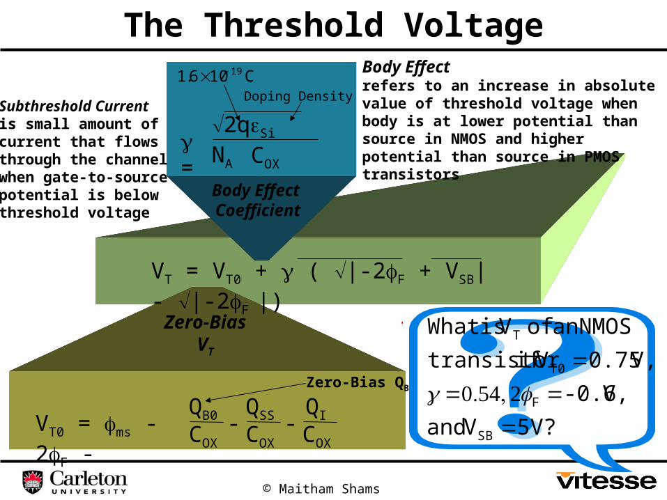
The Threshold Voltage
© Maitham Shams 2002
VT = VT0 + ( |-2F + VSB| - |-2F |)
VT0 = ms - 2F -QB0
COX-
QSS
COX-
QI
COX
Zero-Bias QB
Zero-Bias VT
= 2qSi NA
COX
Body Effect Coefficient
Body Effectrefers to an increase in absolute value of threshold voltage when body is at lower potential than source in NMOS and higher potential than source in PMOS transistors
C 106.1 19Doping Density
5V?V and
V, -0.6
V, 0.75V if transistor
NMOS an of V isWhat
SB
F
T0
T
Subthreshold Currentis small amount of current that flows through the channelwhen gate-to-sourcepotential is belowthreshold voltage

MOS I – V Relations
© Maitham Shams 2002
ID as a function of VDSID as a function of VGS
ID (mA)
VDS (V)
Triode
Saturation
GSV = 5V
VGS = 4V
VGS = 3V
VGS = 2V
VGS = 1V
1
2
0 54321
VDS = VGS - VT
ID
VGS
(V)VT
0.0 1.0 2.0
0.010
Subthreshold Current
0.020 VDS = 5V
Channel Length Modulation Refers to the fact that due to the enlargement of depletion layer on the drain side and, hence, reduction of channel length, ID slightly increases as VDS increases in saturation

Simple MOSFET Model
© Maitham Shams 2002
G
S
ID
D
VDS > VGS – VT Saturation
Square Law:
ID = ( VGS - VT)2(1 + VDS)k’n
L
W
VDS < VGS – VT Linear
ID = {( VGS - VT)VDS - k’n
L
W
2
VDS2
}
W
Drain
Sourc
e
L
Gat
e
Designers usually change size (usually width) of transistor to get the right amount of current
Saturation (ON) and cut-off (OFF) are the more important modes in operation of digital circuits
oxnn CK '
Process transconductance parameter
n Is electron mobility, about 3times larger than hole mobility
MOS technologies are known by their Feature Length (minimum allowable L)
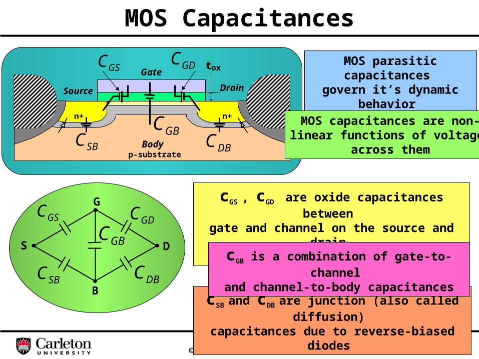
MOS Capacitances
© Maitham Shams 2002
cGS , cGD are oxide capacitances between gate and channel on the source and drain
sides, respectively
cSB and cDB are junction (also called diffusion) capacitances due to reverse-biased diodes
G
S
B
D
GSC GDC
SBC DBC
GBC
n+ n+
Source Drain
p-substrate
Gatetox
BodySBC DBCGBC
GDCGSC MOS parasitic capacitances govern it’s dynamic
behavior
MOS capacitances are non-linear functions of voltages
across them
cGB is a combination of gate-to-channel and channel-to-body capacitances
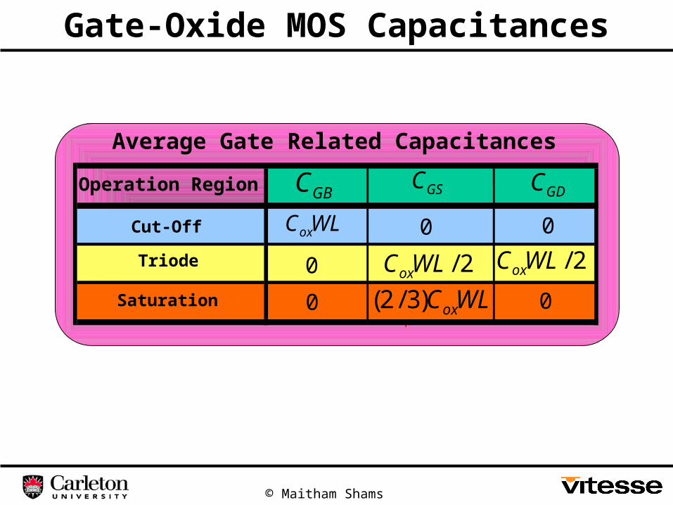
Gate-Oxide MOS Capacitances
© Maitham Shams 2002
Average Gate Related Capacitances
Operation Region
Cut-Off
Triode
Saturation
GSC GDCGBC
0
0
0
0
0
WLCox
2/WLCox 2/WLCoxWLCox)3/2(

Junction Capacitance
© Maitham Shams 2002
linear junction
abrupt junctionCj (fF)
VD (V)
0.00.0
0.5
1.0
2.0
Average value of Cj between VH and VL
Ceq = Qj / VD = Keq Cj
Keq = - 0
m
(VH – VL)(1-m)
x [(0 – VH )1-m – (0 – VL )1-m]
Cj = Cj0
(1 – VD / 0)m
Junction capacitance at zero bias given per unit area
Grading coefficient 0.5 for abrupt junction 0.3 for linear junction
Junction behaves like a capacitance becomes its charge depends on the voltage across it

Non-ideal Behaviour of MOSFET
© Maitham Shams 2002
- Power Law for Sub-micron MOS in Saturation ID = W(VGS – VT), 1.25
Short Channel Effects: Velocity Saturation
and Mobility Degradation
Threshold variations
Parasitic Resistances
Subthreshold current
Latch up

The Threshold Voltage
© Maitham Shams 2002
Example:
VT0 = 0.75 V, = 0.542 F = -0.6V, VSB = 5VVT = 1.6V > 2VT0


![2005 - PLD - Tips Para Uso Eficiente de PLD[1]](https://img.pdfslide.net/doc/110x75/557201054979599169a0911d/2005-pld-tips-para-uso-eficiente-de-pld1.jpg)