Embed Size (px)
Citation preview
* 1985-1986 JSIS Newsletter Index
The 1985-1985 JSIS Newsletter Index is a quick reference guide to the EIEJ and JSIA newsletters. It is structured as follows:
• Titles are organized by both keyword and company.
Pages 2 to 3 are a company list, e.g., LSI Logic.
Pages 4 to 9 are a subject list, e.g., ficonomy.
• The newsletter type, month, and year follow each title listing in the index. Refer to the EIEJ or JSIA tab, month, and year to locate a specific newsletter.
This index is updated quarterly.
JSIS Newsletters 1987 Dataquest Incorporated March
1985-1986 JSIS Newsletter Index 4 Corrpany Date
Newsletter
ADVANCED MICRO DEVICES
Advanced Micro Device's Aimual Shareholders ' Meeting Sony Joins Hands with AMD
EXAR INTEGRATED SYSTEMS
Exar Holds F i r s t Annuad Shareholders ' Meeting
FAIRCHLD SEMICONDUCTOR
The Superal l iance: Fuji tsu Buys 80 Percent of Pair chi ld
FUJTSU LTD.
The Superal l iance: Fuji tsu Buys 80 Percent of Fai rchi ld
HEWLETT-PACKARD CO.
Toshiba Builds R&D Bridge
HITACH LTD.
Hitc«:hi Unveils Plan to Ease Trade F r i c t i o n
LSI LOaC CORP.
How t o Succeed in ASICs: Industry Leaders Share Their Thoughts Venturing in to Japan: How LSI Logic Opened I t s Doors in Tokyo
MITSUBISHI a£CTRIC CORP.
The New Mitsubishi Saijo Factory—A Fully Autonated Fac i l i t y
MONOUTHC MEMORES INC
How t o Succeed in ASICs: Industry Leaders Share Their Thoughts
MOTOROLA INC.
JSIA Sept- 86 JSIA Feb. 86
JSIA Sept. 86
JSIA Oct. 86
JSIA Oct. 86
JSIA Oct. 85
JSIA July 85
JSIA Feb. 86 JSIA May 85
JSIA Oct. 85
JSIA Feb. 86
How to Succeed in ASICs: Industry Leaders Stiare Their Thoughts JSIA Feb. 85
1987 Dataquest Incorporated March JSIS Newsletters
1985-1986 JSIS Newsletter Index
Company Newsletter Date
NATIONAL SEMICONDUCTOR CORP.
National Ca^ iva t e s I t s Reps jSiA Oct. 86 Entering the Japanese Market: NMB Semiconductor and National Sign JSIA Sept. 86
Foimdry
NMB SQVBCONDUCTOR
Entering the Japanese Market: NMB Semiconductor and National Sign JSIA Sept. 86 Foundry
OKI B-ECTRIC INDUSTRY CO. LTD.
How t o Succeed in ASICs: Industry Leaders Share Their Thoughts JSIA Feb. 86
SONY CORP.
Sony Joins Hands with AMD jSIA Feb. 86
TEXAS INSTRUMENTS
HOW t o Succeed in ASICs: Industry Leaders Share Their Thoughts JSIA Feb. 86
TOSHBA ELECTRIC CO.
Toshiba Builds R&D Bridge JSIA Oct. 85
VLSI TECHNOLOGY INC.
How t o Succeed in ASICs: Industry Leaders Shaure Their Thoughts JSIA Feb. 86
JSIS Newslet ters 1987 Dataquest Incorporated March
1985-1986 JSIS Newsletter Index
Subject Date
ALUANCES
Newsletter
Sony Joins Hands with AMD Japanese and European Semiconductor Agreements
ASICS
How to Succeed in ASICs: Industry Leaders Share Their Thoughts
ASSOaATIONS
Ninth Annual SIA Forecast Dinner: Forecasting the Recovery
AUTOMOTIVE
Japan Forms New Autcanotive Materials Research Project
CARTAL EXPENDITURES
1986 Capital Spending: Stormy Weather in Japan Sends Clouds Over Industry
Japanese Market Update—Current Outlook
CAPTIVE
Japanese Captive Semiconductor Sales: An Overview
COI^FERBJCES
Dataquest's 2nd Annual Conference: Future VLSI and Amplications 1985 Japanese Electronics Show Worldwide Technicaa Meetings Dataquest's Japanese Conference Debut—Far East Industry Japanese End Market Analysis Japanese Semiconductor Market Update Japanese Market Update—Current Outlook
CONSUMER
Table 6, Estimated Non-Japanese VTR Production Table 5, Top Five Japanese Manufacturers of VTRs in 1985 Table 4, Semiconductor Contents in VTR
JSIA Feb. 86 JSIA Jan. 86
JSIA Feb. 86
JSIA Sept. 85
JSIA Mar. 86
JSIA June 86
JSIA June 85
JSIA Jime 86
JSIA May 86 JSIA Dec. 85 EIEJ Sept. 85 JSIA May 85 JSIA Oct. 85 JSIA Sept. 85 JSIA June 85
JSIA June 86 JSIA June 86 JSIA June 86
1987 Dataquest Incorporated March JSIS Newsletters
1985-1986 JSIS Newsletter Index
Subject Newdetter Date
CONSUNPTIGN DATA
1986 Japanese Capital Spending Revised Downward: The Gloom Deepens JSIA Dec. 85 TaiJle 2, Estimated Japanese Semiconductor consumption JSIA June 86 Ciy End-Use Category
Semiconductor Amplications: Second Quarter Update JSIA June 86 Japanese Semiconductor Market Quarterly Update: Right on Course JSIA May 86 Vtorld Consumption Update: Semiconductor Consumption Relaounds JSIA Mar 86 in 1986
Semiconductor Consumption in Japan Explodes in 1984 JSiA Mar. 85 New Trends in Semiconductor Distributicm JSIA Mar* 85
DISTRIBUTION
New Trends in Semiconductor Distribution JSIA Mar. 85
DYNAMIC RAM
256K DRAM Dumping Margins Announced jSIA Mar. 86
ECONOMY
Japanese Semiconductor Market Quarterly Update: High Yen Masks JSIA Oct. 86 a Depressed Market
Japanese Semiconductor Market Quarterly Update: High Yen wreaking JSIA Aug. 86 Havoc on Japanese Consumption
The Double wnamray: Yen Appreciation and U.S. Dumping Margins JSIA May 86 Japanese Semiconductor Market Quarterly Update: Right on Course JSIA May 86 The U.S. Economy: Boom or Bust? JSIA NOV.
Japan Plans New Market-Opening Measures EIEJ Sept. Semiconductor Gardening: Japan's Response to the Current Downturn JSIA July*
EDP
85 85 85
IC Cards: The Next PC Boom? j s i ^ Q^t. 86 The Smart IC Card—Market Overview jSi;^ Sept. 86
EMERQNG TECHNOLGQES
Symposium Highlights Latest GaAs IC Developments JSiA Nov. 86
B'ROM
EPROM Dumping Margins Announced JSIA Mar. 86
JSIS Newsletters 1987 Dataquest Incorporated March 5
1985-1986 JSIS Newsletter Index
Subject Newsletter Date
GAAS
The ECL-GaAs Race i n Japan: MITI's Pro jec t Spins off New Device JSIA Feb. 86 GaAs ASIC and Foundry Act iv i t i e s Spur Systems Development JSIA Jan. 86 Seventh Aimual GaAs Symposium, November 12-14, 1985 JSIA Nov. 85
GATE ARRAYS
Venturing into Japan: How LSI Logic Opened its Doors in Tokyo JSIA May 85
GOVERNMEITr
Japan Plans New Market-Opening Measures EIEJ Sept. 85
II^USTRY
Turning the Tide: U.S. Semiconductor Activities in Asia JSIA Sept. 85
II^USTRY TRENDS
Korean Semiconductor Cooperative Research Project JSIA Nov. 86 Japanese Microdevice Industry Update—CMOS Technology is JSIA June 86 Driving Force
Japanese Semiconductor Technology Trends—Fourth Quarter 1985 JSIA Feb. 86 Japanese Technology: The Future Wave JSIA Jan. 86 1985 Japanese Electronics Show JSIA Dec. 85 Japanese Semiconductor Technology Trends—Third Quarter 1985 JSIA Nov. 85 Ninth Annuaa SIA Forecast Dinner: Forecasting tJie Recovery JSIA Sept. 85 Japanese Semiconductor Market Update JSIA Sept. 85 Japanese Semiconductor Technology Trends—Secraid Quarter 1985 JSIA Aug. 85 Japanese Semiconductor Technology Trends—First Quarter 1985 JSIA June 85 Dataquest's Japanese Conference Detjut—Far East Industry JSIA May 85 Japanese Semiconductor Technology Review—Fourth Quarter 1984 JSIA Jan. 85
INFORMATION SOURCES
Successful Intelligence Gathering: Dataquest's Recipe JSIA Mar. 85
ISSCC
The ECL-GaAs Race in Japan: MITI's Project Spins off New Device JSIA Feb. 86 Japcm Takes Center Stage at ISSCC 1985 JSIA Mar. 85
KOREA
Korean Taxation EIEJ Apr. 86
& 1987 Dataquest Incorporated March JSIS Newsletters
1985-1986 JSIS Newsletter Index
Subject Newsletter Date
MANUFACTUrai^«3
Semiconductor Ifenufacturing Equijanent: Can the United States Remain Competitive?
MAfJKET SHARE
Table 3, Estimated Share of Japanese Semiconductor Market by
End-Use Category
Vtorld Consumption Update: Semiconductor Consumption E^aounds in 1986
Preliminary 1985 Japanese Company Market Snare Estimates The Japanese Market: Sales by All Manufacturers in 1985 Japanese Market Update—Current Outlook Japanese Semiconductor Activity in the United States—1984 Update Preliminary 1984 Market Share Estimates
MARKETS BY END USER
Japanese Semiconductor Application Trends Second Quarter 1986 Japanese Semiconductor Application Trends First Quarter 1986
MERGERS & ACQUISITIONS
The Superalliance; Fujitsu Buys 80 Percent of Fairchild
MICROPROCESSOR
Japanese Microdevice Industry Update—CMOS Technology Is Driving Force
MIUTARY/H RBL
EIEJ May 85
JSIA
JSIA
JSIA JSIA JSIA JSIA JSIA
June
Mar.
Dec. June June Feb. Jan.
86
86
85 85 85 85 85
JSIA NOV. 86 JSIA Sept. 86
JSIA Oct. 86
JSIA June 86
Japan ' s Expanding Space Programs Demand Hi-Rel iCs
MITI
JSIA Nov. 86
MITI Offers Proposal t o Avoid Dumping Penal t ies
OPTOELECTRONICS
Japan ' s E>ush in to Optocomputing: Makers Form Opto C3onsortium
OTHER MBVIORY MARKETS
Signi f icant Product Announcements—GaAs ICs Gallium Arsenide ICs—Fact or Fancy?
JSIA May 86
JSIA May 86
JSIA Oct. 86 JSIA Sept. 86
JS IS N e w s l e t t e r s 1987 D a t a q u e s t I n c o r p o r a t e d March
1985-1986 JSIS Newsletter Index
JSIA JSIA JSIA JSIA JSIA JSIA JSIA JSIA JSIA
May Feb. Jan. Jan. Nov. Oct. Aug. June Mar.
86 86 86 86 85 85 85 85 85
Subject Newsletter Date
PRODUCTION DATA
Table 1, Estimated Japanese Electronic Equipment Production JSIA June 86 Japanese Industrial Electronics Production to Reach yil.3 Trillion JSIA Dec 85
in 1989 1984 Construction Boom Creates Over-Capacity JSIA Oct. 85 Japanese Electronic Equipment Production to Reach 118 Trillion JSIA Oct. 85 in 1990
R8iD PROJECTS
Japan's Push into Optocomputingj Makers Form Opto Consortium Japanese Semiconductor Technology K"ends—Fourth Quarter 1985 Joint RStD Projects Japan's Shift to Iimovation: A Bocan in Basic Research Labs Japanese Semiconductor Technology Trends—Tliird Quarter 1985 Toshiba Builds R&D Bridge Japanese Semiconductor Technology Trends—Second Quarter 1985 Japanese Semiconductor Technology Trends—First Quarter 1985 Japan Takes Center Stage at ISSCC 1985 Japanese Semiconductor Technology Review—Fourth Quarter 1984 JSIA Jan. 85 ROW
Doing High-Technology Business in Korea JSIA July 86 Dataquest's Japanese Conference Debut—Far Eaist Industry JSIA May 85
SHARES OF REGONAL MARKETS
Dataquest Announces Final 1985 Japanese Semiconductor Market Share JSIA Sept. 86 Figure
SHIPMENT DATA
Japanese Industrial Electronics Production Forecast At 12.5 JSIA Dec 86 Trillion Yen
Japanese Semiconductor Activity in the United St:ates—1984 Update JSIA Feb. 85
STANDARD CELL
Megacell Fever: Japanese Developing Autcsnated Standard JSIA Mar. 86 Cell Systems
START-UPS
The Third Wave: The Surge in Semiconductor Start-Ups Continues JSIA Oct. 85 The Semiconductor Start-Up Boom Continues JSIA May 85
9 1987 Dataquest Incorporated March JSIS Newsletters
1985-1986 JSIS Newsletter Index
Subject Date
SUPffJCOMPUTBR
i^wsletta*
The ECL-GaAs Race in Japan: MITI's Project Spins off New Device Table 4 , 1985 Japanese Supercomputer A c t i v i t i e s
TECHNICAL EXCHANGES & SECOND SOURCE
JSIA Feb. 86 JSIA Feb. 86
Entering The Japanese Market: NMB Seniconductor and National Sign JSIA Sept . 86 Foundry
U.SIJAPAN
U.S.-Japan Semiconductor Trade Update: Second Quarter 1986 Fallout from the U.S.-Japan Chip Agreement: Japan's Shift to Innovative Products
Improving International Ccanpetitiveness: A Dataquest View U.S.-Japan Semiconductor Trade Update: First Quarter 1986 New Semiconductor Accord: Yeutter's Present to Manufacturers The Double Whammy: Yen Appreciation and U.S. Dumping Margins MITI Offers Proposal to Avoid Dumping Penalties EPROM Dumping Margins Announced 256K DRAM Dumping Margins Armounced
Preliminary 1985 U.S.-Japan Semiconductor Trade Estimates Ninth Annual SIA Forecast Dirmer; Forecasting the Recovery Turning the Tide: U.S. Semiconductor Activities in Asia U.S. and Japanese Semiconductor Industry Interrelationships Hitachi Unveils Plan to Ease Tracte Friction U.S.-Japan Semiconductor Trade Update—First Quarter 1985 Venturing into Japan: How LSI Logic Opened Its Doors in Tokyo U.S.-Japan Trade: East Leads West Semiconductor Consumption in Japan Ejcplodes in 1984 Japanese Semiconductor Activity in the U.S.—1984 Update
JSIA JSIA
JSIA JSIA JSIA JSIA JSIA JSIA JSIA JSIA JSIA JSIA JSIA JSIA JSIA JSIA JSIA JSIA JSIA
Nov. Oct.
Aug. Jione June May May Mar. Mar. Jan. Sept. Sept. July July July May Apr. Mar. Feb.
86 86
86 86 86 86 86 86 ^ 86 85 85 85 85 85 85 85 85 85
JSIS Newsletters 1987 Dataquest Incorporated March
1985-1986 JSIS Newsletter Index
(Page intentionally left blank)
10 1987 Dataquest Incorporated March JSIS Newsletters
THE U.S. ECONOMY: BOOM OR BUST?
In a recent visit to DATAQUEST, Joseph W. Duncan, Corporate Economist and Chief Statistician of the Dun & Bradstreet Corporation, shared some of his views on the future of the U.S. economy. Due to the universal nature of the subject matter and the impressive credentials of Mr. Duncan, we believe that his views would be of interest to our clients. Mr. Duncan worked eight years as the chief statistician for the Office of Information and Regulatory Affairs of the U.S. Office of Management and Budget. Previously, he was a research and management specialist at Battelle Memorial Institute where he spent 13 years. Mr. Duncan's education includes receiving a B.S.M.E. degree from Case Institute of Technology, an M.B.A. degree from Harvard Graduate School of Business Administration, and a Ph.D. degree in Economics from Ohio State University. He also attended the London School of Economics.
KEY ECONOMIC ISSUES
With respect to the health of the U.S. economy, Mr. Duncan identified three key questions:
• Will there be a recession in the near future?
• Will activity continue in capital markets?
• Will Congress act to reduce the budget deficit?
Recession
In order to address the likelihood of a recession, one must address the health of principal components of the economy. These vital components are consumer spending—which makes up approximately two-thirds of the GNP—housing starts, business starts/failures, unemployment, capital spending, and inflation.
Consumer spending is expected to remain strong. Contrary to widely held beliefs, Mr. Duncan believes that consumers are not over-extended because monthly payments remain a small percentage of disposable income. The housing market appears to be garnering pent-up demand, as mortgage rates have remained at the pivotal 12 percent for some time now. Rates are expected to drift down below 12 percent, however, which should trigger a very strong housing market.
1985 Dataquest Incorporated Nov. 22-Reproduction Prohibited
JiA cofit«fTt pt thii tupofX ni^&^t\is OUT Interprdlaitir^ Arvd Ai>i(Jv!ii& ni iit\orma\jan ^nerjujy avoitpbh^ in iTia puDlK or i[>loft3^ t>y m&ponBttile intfiubOuAlD in ihs . u b ^ ] conifNinifiB. tiiit ut runt f^wntnta^ ftt iti accuracy V cmnpHJitt^iuia n dDasnd cnr<tsin niaietLal pmvlded to \a In onfiderip? I> (HJI dionta InbivltHtEI cwnfiania^ reporred oi\ ana analyza) biy {>ATAOUEST. r^ay I}e cIlQf la o< Itiladnt^or olhtN DATAQUEi^T 4eiVicH. Tlui InTonnatbon.la not rumIallDd k)conr^«tk>rt wllb 1 Sfllfl Of ofle? to sell M[;yf i,hB or ir (?nrTr*c(ktn i*ilh rhp ftjHfllUKjnr ?|1 An nPIiy la buy «ttff?tiofl ThL* iim fli»d Its fwfiinl .ftdror ihejr ofNcora. ?toci<hQldfi(a, « menbaffl flf. tba; FamJIiea RIB/, ttam ttme ro bnie. htri/p a kmn f BfiDrf ocHluan in The ukKuniLAa mflnUDiiad and may B t or bijy Aucb aecLiriiips.
Azabu Heights, Suite 711, 1-5-10 Roppongi, Minato-ku. Tokyo 106, Japan 1290 Ridder Park Drive / San Jose. CA 95131 / (408) 971-9000 / Telex 171973
Business starts are at an all-time high. This bears no correlation to interest rates; rather, it is attributed to a more entrepreneurial spirit and willingness to take risks. While business starts are up, so too are business failures. There are several reasons for this: small businesses pay very high interest rates and are at high risk for failure. Also, liberalized personal bankruptcy laws have made it more acceptable to file bankruptcy claims.
Employment has grown continuously during the last five years. Import activity, which would seem to adversely affect the health of the economy, does, in fact, add jobs in the United States. Thus, import activity together with strengthened demand from overseas markets for U.S. exports, should be bolstered.
Capital Market Activity
Capital spending has been depressed due to uncertainty of its treatment under proposed tax reforms. Yet, Mr. Duncan believes that tax reform will not occur until 1987. Spending is expected to pick up in 1986, along with corporate profits. Corporate cash flow will be up 5 percent in 1985, while profits will be down 5 percent. Inflation will increase as well, but is not expected to exceed a 5 percent annual rate.
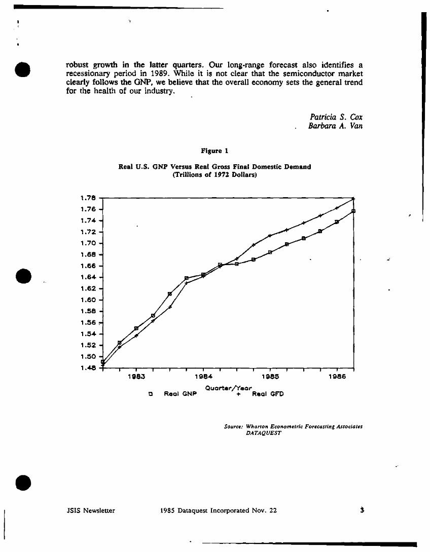
We believe that there are two sides to the U.S. economy: production, expressed as gross national product (GNP) and consumption, which we refer to as gross final domestic demand (GFDD). To get a good view of the economy, one should look at both. GFDD measures the strength of demand in the economy by factoring net exports and inventory change out of GNP: GFDD = GNP - change in inventory + imports - exports. As shown in Figure 1, the GFDD points to a healthy market with 3.3 percent growth between the fourth quarter of 1984 and the third quarter of 1985. Forecasts of real GNP identify growth of 2.7 percent for 1985, 3.5 percent for 1986, and 4.5 percent for 1987. Growth in GFDD is forecast to remain higher than GNP growth through the end of 1985.
Congressional Action
It is highly probable that the U.S. economy will not experience another recession until 1989. If Congress acts to pass a budget balancing bill, the economy should experience moderate growth for several years. However, if the deficit is not reduced, interest rates could start spiraling as early as spring of 1986, and a recession would soon foLiow. We believe Congress will act to balance the budget.
SUMJMARY
Mr. Duncan identifies a healthy U.S. market. DATAQUEST concurs with his assessment and agrees that 1986 will be a healthy year. Our forecast for semiconductor growth assumes light growth in the first quarter of 1986 with more
1985 Dataquest Incorporated Nov. 22 JSIS Newsletter
robust growth in the latter quarters. Our long-range forecast also identifies a recessionary period in 1989. While it is not clear that the semiconductor market clearly follows the GNP, we believe that the overall economy sets the general trend for the health of our industry.
Patricia S. Cox Barbara A. Van
Figure 1
Real U.S. GNP Versus Real Gross Final Domestic Demand (Trillions of 1972 Dollars)
1984 1 I
1985 1 r
1986
Quarter/Year Reel GNP + Real GFD
Source: Wharton Econometric Forecasting Associates DATAQUEST
JSIS Newsletter 1985 Dataquest Incorporated Nov. 22
SEVENTH ANNUAL GaAs SMPOSIUM NOVEMBER 12-14, 1985
Interest in gallium arsenide (GaAs) ICs has grown rapidly in recent years. Attendance at the IEEE-sponsored GaAs IC symposium has grown more than 30 percent annually since 1982, reaching 850 at this year's meeting in Monterey, California. Abstract submittals increased 24 percent over 1984, indicating substantial growth in development activity.
HIGHLIGHTS
General
Forty-nine papers, approximately evenly split among analog ICs, digital ICs, and technology topics
Authors from 26 companies, 5 universities, and 2 other organizations
Three panel discussions covering millimeter-wave ICs, LSI issues, foundry operations, and standardization
Key Papers
A GaAs, 1 2 - b i t , 1-GHz d i g i t a l - t o - a n a l o g c o n v e r t e r (DAC)— Hewle t t -Packard Labs
A 115-GHz, m o n o l i t h i c , GaAs, FET o s c i l l a t o r — T e x a s Ins t rumen t s
A 2 . 6 n s , t ^ a , IK x 4 SRAM us ing enhancement /dep le t ion MESFETs (two p a p e r s ) — H i t a c h i
An ECL-compatible, IK SRAM (with s m a l l e s t c e l l r e p o r t e d t o da t e )—Texas In s t rumen t s
© 1985 Dataques t I nco rpo ra t ed Nov. 19 ed . -Reproduc t ion P r o h i b i t e d
I f l * £i"i!Ill^^.^ftl iriflt I*HK1 HjP'lfM^i« win IT Vrprwinit-^ i i - i i t * -* '
prn^jIiiffrTPIui i'i:flr]|iii*(ir;(,^| mp r i -rni* Vi^-»r^»* tn' i^^*"-^!
« ' In r-r v-JiitTFaTrTTi r r j r taH*^ 1 (• i. ^ tr- ' iH*s ' ' • * •' »'>J .i
I- t n a « i i i < n^iin> tin I A U I > £ M "ur vn.ti^^ : ^'ni- H \:\t •••-\.\nt\* m*^^u't^'' >*•• i
' iHI-||i^ r . ::-'p;iiim* Tnjr . • • - • . r,,,, ^lllrw . . - . . / f- L -nyf t fP ieM H JLTT.tLi}-.ijiliplI*'"niTin• t |
tf\t t S ft fMSnrt jNi^ *> fsH • Li'i'i*J '4M n tVi'iftLf i ti i* * • IH Jl UH* fli'LJ1J*» Ibl^M K*: i lnltEJ UH IPP L LiCint .! Hi;f1
-It^~t<-f^t•i}^^^'^-••W•'^'^^-J^^' " ' f W t * t 1 H*V MiFrlli^finj ^iiC "1*J Vflh iititj^f ^ j ^ ^ Tt^n'ttmf
Dataquest Incorporated, A Subsidiary of A 0. Nielsen Company / 1290 Ridder Park Drive / San Jose, CA 95131 / (408) 971-9000 / Telex 171973
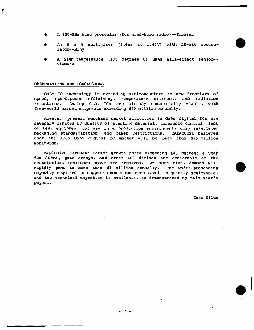
• A 400-MHz band prescaler (for hand-tield radio)—Toshiba
Ii An 8 X 8 multiplier (5.6ns at 1.45V) witti 20-bit accumulator—Sony
• A tiigh-temperature (180 degrees C) GaAs hall-effect sensor— Siemens
OBSERVATIONS AND CONCLUSIONS
GaAs IC technology is extending semiconductors to new frontiers of speed, speed/power efficiency, temperature extremes, and radiation resistance. Analog GaAs ICs are already commercially viable, with free-world market shipments exceeding $50 million annually.
flowever, present merchant market activities in GaAs digital ICs are severely limited by quality of starting material, threshold control, lack of test equipment for use in a production environment, chip interface/ packaging standardization, and other restrictions. DATAQUEST believes that the 1985 GaAs digital IC market will be less than $15 million worldwide.
Explosive merchant market growth rates exceeding 10 0 percent a year for SRAMs, gate arrays, and other LSI devices are achievable as the restrictions mentioned above are resolved. At such time, demand will rapidly grow to more than $1 billion annually. The wafer-processing capacity required to support such a business level is quickly achievable, and the technical expertise is available, as demonstrated by this year's papers.
Gene Miles
- 2 -
SMICONDUCTOR MANUFACTURING EQUIPMENT: CAN THE UNITED STATES REMAIN COMPETITIVE?
INTRODUCTION
The U.S. Department of Commerce (DOC) published a report in March 1985 entitled "A Competitive Assessment of the U.S. Semiconductor Manufacturing Equipment Industry." The report, issued under the auspices of the DOC's International Trade Administration, was authored by the Science and Electronics Office of Microelectronics and Instrumentation and the Assistant Secretary for Trade Development.
The report is an attempt by the Office of Microelectronics and Instrumentation (OMI) to assess the competitiveness of the U.S. semiconductor manufacturing equipment industry. Sources used for the report include officials from the National Bureau of Standards and the Census Bureau, U.S. and European manufacturers, several agencies and associations, publicly available information, and market research companies (including DATAQUEST).
HIGHLIGHTS OF THE REPORT
The report presents historical and forecast market demand by geographic region for wafer processing, assembly, and test equipment. It examines competitive strengths and weaknesses by manufacturing region (United States, Japan, and Europe). The sales figures shown for the major U.S., Japanese, and European semiconductor equipment firms show Japanese manufacturers gaining worldwide market share.
Also examined are the close relationships that exist between major Japanese semiconductor equipment manufacturers and the major Japanese semiconductor suppliers. These relationships can result in preferential treatment for the equipment manufacturers.
© 1985 Dataquest Incorporated May 8 ed.-Reproduction Prohibited
T h
p r o
cont
video o u s m c
s repor
^nhflen
leo'e
ceDy
senI
)urc
h i
U U f
• CMS
V . . P -
n i e r p t e l d t i o
Individual c
, M , , e . T h i .
a-vi a -.
^moarMc
„ m a n „
i > s i s u t : n '
s r t ' p o ' l e d o
IS parent a
c r - a t o - g e ' ' n , , , i i y , v ^ n , i , i . n.
n ana analy?en tiy DATAQUEST
nd/or men oMice's s lotkholder
I f i n n . . > ;;
m a y b e c h e -
o rmempe,
* i , ^ . c i ! ^ , ' ; . < : ; M V ' - i - . . . . - „ . • . - . 7 - . -
s ot this and or other DAI AGUES T servn t
of ihi-1 tai ' i i ' ies .t ia. ii',-.. i.i-r.c v, [ n c <•.
, f - - -
s This 1
• ' • • ' " "
- ^-.-^ 1
0 i-H!. ' "
r - > - , . < .
> • rvu'if»»*hfl'"T*'J *» 1 •' *i-L.ufik • <j" i ^r
. —ii Hj i i i . .4mj bd .1 i i ' . : , • • : « • J fJlH
* »->niI:t%* *r* . i i I 1»: r l •tlirii 1 ,•• AKtiiirli] *
ILIllp!r^tt
. - (n tPHi .Nr
H* ^ Dll
|l III)trk'iHHr;..IjI^14|r
iip^ i.'-t-r-\ IK i'i .-I
T i l t ' l « I j m I i I »
rfl*1«'IJ-
IIPIli.I.Li.
Dataquest Incorporated, A Subsidiary of A C. Nielsen Company / 1290 Bidder Park Drive / San Jose, CA 95131 / (408) 971-9000 / Telex 171973
other topics discussed include R&D and sources of funding, government policies and incentives to industry, government procurement, and tariffs and other trade barriers.
The report concludes by calling for the U.S. government to take the following five measures to aid U.S. competitiveness in the semiconductor manufacturing equipment industry:
Encourage increased investment in R&D
Expand the pool of technical expertise available to the industry
Improve industry/government cooperation
Increase export opportunities for the semiconductor equipment industry
Create an official data base for the semiconductor equipment industry
DATAQUEST CONCLUSIONS
We believe that this report is extremely significant to both the semiconductor equipment industry and the semiconductor component industry. We anticipate that it will spur the government to take steps to increase available information on the industry, specifically, by assigning SIC codes to semiconductor equipment and by developing 5-digit export and import code classifications for this industry.
The report may be ordered from:
Superintendent of Documents U.S. Government Printing Office Washington, D.C. 20402 Phone (202) 275-2051
The cost of the report is $425; it may be ordered by phone and charged on Visa or MasterCard. The report number is 1985-461-105/20066.
Patricia S. Cox
- 2 -
Dataquest JAPANESE RESEARCH NEWSLETTER
EIEJ Code: Newsletters
NTT PURSUES PATENT SALES AND JOINT R&D
SUMMARY
At a recent presentation at Stanford University's U.S.-Asia Forum, Hideaki Toda, Director General of the New York office of Nippon Telegraph and Telephone (NTT), discussed forthcoming changes in NTT policies that DATAQUEST believes will have a major impact on the semiconductor industry. The discussion focused on three key issues;
• NTT privatization (entry into the commercial market)
• Patent sales and joint R&D
• Business opportunities in the value-added network (VAN) market
NTT PRIVATIZATION
Currently, the Japanese Diet is considering the NTT Company Limited Bill that would allow NTT to compete in the Japanese telecommunications market as a privately owned company. NTT is now a government-controlled monopoly. Known as "privatization," the bill would make the following changes in NTT management:
Government stock ownership limited to one-third
Limited government regulation
No government control over NTT budget
No restrictions on investunents
No government financial assistance; free access to the capital market
1984 Dataquest Incorporated Nov. 1 ed.-Reproduction Prohibited
The content of this report represents our interpretaion and analysis of information generaIIy avaiIable to the public or released by responsible individuals in the subject companies, but is not guaranteed as to accuracy or completeness It does not contain material provided to us in confidence by our clients individual companies reported on and analyzed bv DATAQUEST, may be clients of this and/or other DATAQUEST services This information is not furnished in connection with a sale or offer to sell securities or in connection with the solicitalIon of an otter to buy securiiies Tnis rirm ana its parent and/or ihsir officers, stockholders, or members of their families may from time to time, have a long or short position in the securities mentioned and may sell or buy such securities
Azabu Heights, Suite 711, 1-5-10 RoppongI, MInato-ku, Tokyo 106, Japan 1290 Bidder Park Drive / San Jose, CA 95131 / (408) 971-9000 / Telex 171973
l^ ^
• strikes allowed under certain restrictions
• Government review of NTT operations within five years to ensure compliance with legislative goals
Mr. Toda noted that NTT privatization differs from AT&T divestiture because NTT will remain intact and will not be broken up into separate operating companies. Nevertheless, NTT expects to encounter strong competition from the newly formed Second NTT Planning Company (see our EIEJ newsletter dated May 30 1984, "A Second NTT Takes Shape") and from members of the "NTT Family," such as NEC, Fujitsu, and Hitachi. Mr. Toda also believes that foreign companies will play increasingly important roles as suppliers and competitors in this market. Under Hisashi Shinto, president of NTT, the company increased procurement of foreign-produced equipment to $140 million in 1983.
PATENT SALES AND JOINT R&D
A major policy change is NTT's decision to sell its patents and to conduct joint R&D with non-Japanese companies. NTT recently established a subsidiary called NTech, which sent letters to U.S. companies offering to sell NTT patents. There was little response, however, despite NTT's high level of expertise in Japanese semiconductor technology. DATAQUEST believes that this is an excellent opportunity for semiconductor companies interested in securing NTT technology. For advanced technologies, such as megabit DRAMs, GaAs digital ICs, and semiconductor lasers, NTT will conduct joint R&D through its Track III procurement procedure (see our JSIA newsletter dated February 22, 1984, "NTT Discloses its Adoption Standards to Foreign Semiconductor Suppliers"). NTT also will provide publicly available technical documents and encourage technical exchanges with researchers at its four laboratories.
BUSINESS OPPORTUNITIES IN THE VAN MARKET
The Telecommunications Bill, which would deregulate the Japanese telecoimnunications market, is expected to pass in the Diet next year. The legislation would abolish the primary telephone concept and deregulate value-added network (VAN) services, thus opening the market to domestic and foreign competition. Under the bill, three types of carriers would be recognized by the Ministry of Posts and Telecommunications, as shown in Table 1.
Non-Japanese companies such as AT&T, IBM, and GTE-Telenet have entered the market as resellers to provide VAN services and are working with their Japanese partners (see our JSIA newsletter dated October 19, 1984, "The Next Generation: Japan's Information Network System (INS)"). DATAQUEST believes that this area will open numerous opportunities for semiconductor makers selling telecommunications, ICs, logic and memory devices, and optoelectronics.
- 2 -
FOR MORE INFORMATION
For more information about NTT procurement procedures, joint R&D opportunities, or patent sales, please contact the following offices:
• Head Office
- Nippon Telegraph & Telephone 1-6, Uchisaiwaicho 1-chome, Chiyoda-ku Tokyo 100 Japan Tel: (03) 509-5111
• Overseas Offices
NTT New York Office Pan American Building, Suite 2905 200 Park Avenue, New York, NY 10166 U.S.A. Tel: (212) 867-1511
NTT Silicon Valley Office 4962 El Camino Real, Suite 230 Los Altos, CA 94022 U.S.A. Tel: (415) 940-1414
NTT London Office 2nd Floor, Adelaide House, London Bridge London, EC4R 9BU, United Kingdom Tel: 623-8340
,- NTT Office de Geneve 30 Chemin du Pommier, 1218 Grand-Saconnex Geneva, Switzerland Tel: 98-3840
Sheridan Tatsuno
- 3 -
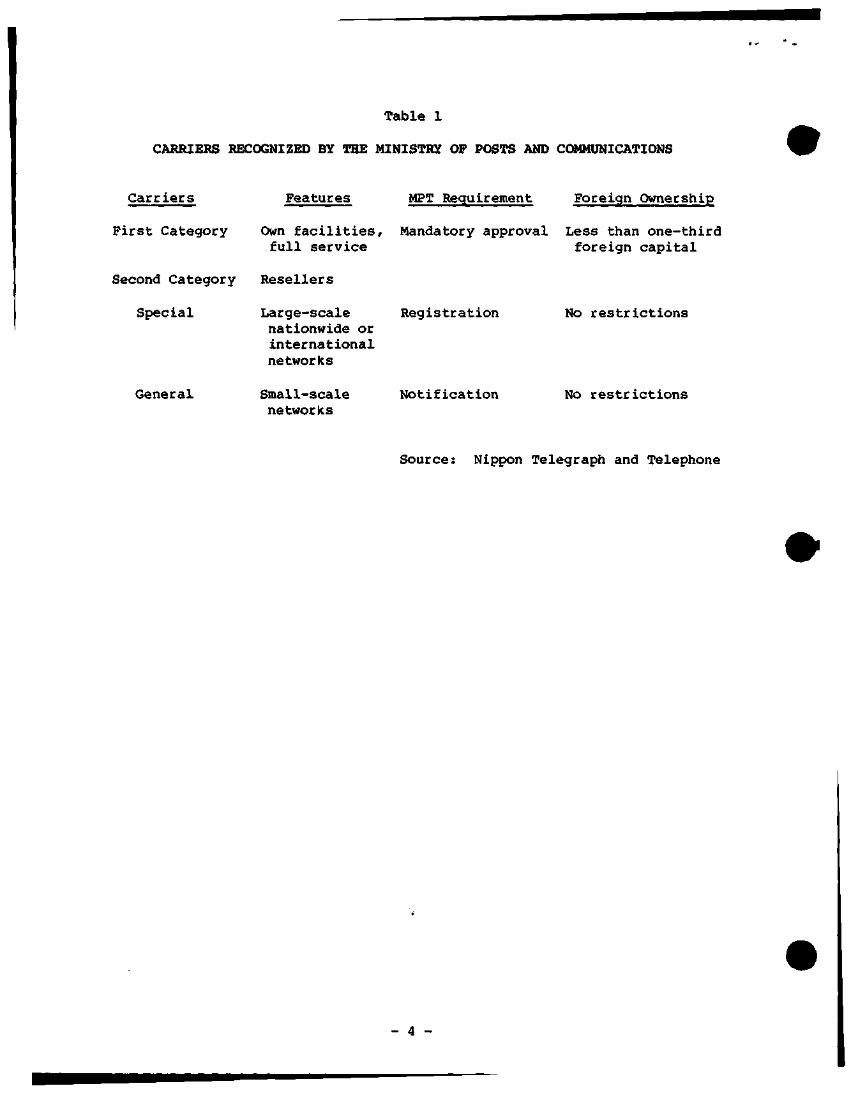
Table 1
CARRIERS RECOGNIZED BY OTE MINISTRY OP POSTS AND COMMUNICATIONS
Carriers
First Category
Second Category
Special
General
Features MPT Requirement Foreign Ownership
Own facilities. Mandatory approval Less than one-third full service foreign capital
Resellers
Large-scale Registration nationwide or international networks
No restrictions
Small-scale networks
Notification No restrictions
Source: Nippon Telegraph and Telephone
- 4 -
EIEJ Code: Newsletters
HITACHI ANNOUNCES CAD SYSTEM FOR THREE-DIMENSIONAL ANALYSIS
REVOLUTIONARY DEVELOPMENT
The era of three-dimensional computer-aided design (CAD) has arrived. On October 19, Hitachi became the first Japanese semiconductor maker to announce CAD equipment and software for developing next-generation VLSI devices such as 1Mb to 64Mb DRAMs and high-function MPUs. Announced by Hitachi's Central Research Laboratory, the CADDETH software program is capable of displaying 3-dimensional color images of the electrical and physical properties of VLSI circuits. The software can be run on Hitachi's supercomputer, the Hitac S-810/20, which has a peak operating speed of 360 megaflops (million floating-point operations per second). Running the program on existing computers takes at least a day, or one hundred times as long.
Unlike current CAD systems, which are only able to display two-dimensional images of devices with geometries of over 1 micron, the Hitachi system can visually display the following conditions:
Electrical characteristics of CMOS and bipolar circuits
Effects of external heat buildup
CMOS latch-up analysis
PN junction destruction phenomena
High-speed reliability tests
High- and low-temperature conditions
According to Dempa Shimbun, Japan's daily electronics journal, other Japanese semiconductor makers are racing to develop comparable systems, but they are encountering the problems of long processing times and displaying the analysis results in an easy-to-understand format.
© 1984 Dataquest Incorporated Oct. 29 ed.-Reproduction Prohibited
Tne conte
P-^' dOHl
ni of th is report represenis our
3 us 1 . conl . r lpnrebv our ' ; l ie ' ' l ^
^l icirat.nn r.t an oHer to buy sei.
nierpreiat i
Intl.v.nual
unties. Thi
Dn and arialysi
-or^paniP-i-ep
( i r m a n d . l s p
ol intormanon genera
o - ' e a o n a - a a n a i v z e o b .
,en iand io , mei ro l l i cer
ya .a . i aB ie .o
DATAQUESl
, M o c k M l d e ,
he pu
mayo
o. m
I.COI
eLi ien
emoer
e leasedb
s o l l h i s a
o i i n e i . - a
respon
nd'of oin m.-iesm
ible indiviauals m ihe subject companies bui 15 n
er D A T A Q U E S T services This iritortnation 15 nol (
ay Irom lirne lo l ime nave a long or sr'Ort posinui
ot guaranteed as toaccu
rnishedir i c o n n e c t i o n s
, n , „ . , ^ c . . , i i e . r r ; . . . | , 0
a c y o
ih a 5
L^dar
completeness
ale or otter lo sel
J ^3> tev 0 ' b-v
t does no
sec^ri l ie
su rh ^i^r
contain
or in con
ir.ties
Tiaterial
nection
Dataquest Incorporated, A Subsidiary of A.C. Nielsen Company / 1290 Bidder Park Drive / San Jose, CA 95131 / (408) 971-9000 / Telex 171973
VERTICAL INTEGRATION REVISITED
DATAQUEST observes that Hitachi is making a strong push into semiconductor equipment. We have determined that during 1983, Hitachi applied for 58 patents for semiconductor manufacturing equipment, second only to Fujitsu, which had 75. (See the JSIA newsletter "Japanese Semiconductor Technology Review, Second Quarter 1984," dated August 17, 1984, for the complete story on Japanese semiconductor equipment patents.)
Furthermore, on June 1, the company established a new company, Hitachi VLSI Engineering, at its Central Research Laboratory in Kokubunji to develop next-generation semiconductor technology. In June, Hitachi announced a transmission electron microscope capable of ultrahigh resolution photography up to 0.72 angstroms. The microscope will be used for developing superlattice-structure semiconductors, amorphous metal, fine ceramics, and other new materials.
In June, Hitachi also announced plans to invest ¥110 billion ($460 million) in its semiconductor divisions in fiscal 1984, 75 percent ($83 million) of which will be spent on semiconductor manufacturing equipment, including clean rooms. Hitachi plans to produce 60 percent of all the semiconductor equipment used in-house, or about ¥50 billion ($206 million), up from 40 percent in fiscal 1983. A new building is being constructed at its Naka plant to produce semiconductor manufacturing equipment.
CONCLUSIONS
DATAQUEST believes that Hitachi's recent announcement is significant because of its potential impact on the development of next-generation semiconductor technology. Not only can the new software be used for developing megabit DRAMs and high-function MPUs, but also superlattice devices, three-dimensional ICs, optoelectronic ICs, and possibly GaAs heterojunction devices in the future. Since Hitachi is a participant in MITI's New Semiconductor Functions Project, we believe that it will use three-dimensional display CAD software for developing three-dimensional ICs. Hitachi's CADDETH software also underscores the growing role of supercomputers in next-generation semiconductor research.
Sheridan Tatsuno
- 2 -
Dataquest JAPANESE RESEARCH NEWSLETTER
EIEJ Code: Newsletters
MITI'S TAKE-LEAD STRATEGY SHIFTS INTO HIGH GEAR
SUMMARY
Despite denials to the contrary, Japanese industrial policies are alive and well. In an effort to regain its former influence over the electronics industry, the Ministry of International Trade and Industry (MITI) has issued a series of industrial policies designed to promote public and private research in high-technology industries. As shown in Figure 1, DATAQUEST believes that these policies are part of MITI's overall strategy to give Japanese industry a competitive advantage over the West and rapidly emerging South Korea, while at the same time trying to reduce trade conflicts. This year, MITI has announced policies that we believe will have a major impact on the semiconductor industry. These policies cover the following areas:
• High-Technology Policies
Overall MITI policy direction
MITI fiscal 1985 budget proposal
• Financial Incentives
Tax breaks for high-technology industries
Venture Business Promotion Law
- Japan Development Bank loans
Export-Import Bank of Japan loans
New media loan program
• Government R&D Activities
Sale Of MITI patents
100-Mbyte DRAM project proposed
© 1984 Dataquest Incorporated Oct. 26 ed.-Reproduction Prohibited
The content of this report represents our interpretaion and analysis ot information generally available to the public or released by responsible individuals in the subject companies, but is not guaranteed as to accuracy or completeness. It does not contain material provided to us in confiIJence by our clients Individual companies reported on and analyzed by DATAQUEST, may be clients of this and/or other DATAQUEST services This information is not furnished in connection with a sale or offer to sell secuntios or in connection with the solic'tation of an offer to buy securities This firm and its oarent and/or tneir onrcers, STocKnoiaers, or memoers of their families may, from time to time, have a long or short position in the securities mentioned and may sell or buy such secunties
Azabu Heights, Suite 711, 1-5-10 Roppongi, Minato-ku, Tokyo 106, Japan 1290 RIdder Park Drive / San Jose, CA 95131 / (408) 971-9000 / Telex 171973
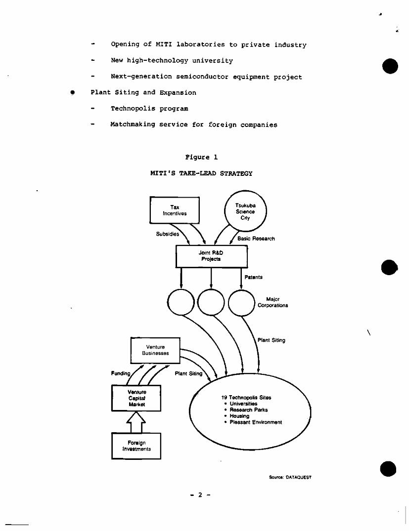
Opening of MITI laboratories to private industry
New high-technology university
Next-generation semiconductor equipment project
Plant Siting and Expansion
Technopolis program
Matchmaking service for foreign companies
Figure 1
MITI'S TAKE-LEAD STRATEGY
Tax Incentives
Subsidies^^
1
\ / Joint R&D Projects
•
Tsuituba \ Science J
City /
/ Basic Research
Patents
\ Major / Corporations
Funding
Foreign Investments
Source: DATAQUEST
- 2 -
HIGH-TECHNOLOGY POLICIES
Overall MITI Policy Direction
"High technology" is the buzzword at MITI this year. Based on private industry surveys, MITI has identified three industries for accelerated development: microelectronics, new materials, and biotechnology. In a recent interview with the Japan Economic Journal, new MITI vice minister Keisuke Konaga emphasized Japan's need for innovative research; "Up to now, Japan's technological development has relied heavily on using foreign technology. Such a pattern will not be allowed to continue. We will have to make original developments on our own. We will push technological advances with creative and problem-solving type people. This will involve a greater risk, a longer development period, and far more financial resources than in the past. While the main propellant of technological development is the private sector, the government needs to cooperate under an appropriate scheme of burden-shar ing."
DATAQUEST observes that Japan's top semiconductor makers are already focusing on the development of original 32-bit MPUs, advanced VLSI, gate arrays, standard cell libraries, CAD software, GaAs digital ICs and microwave devices, optoelectronics, three-dimensional ICs, and bioelectronics. MITI is supporting these private efforts with its R&D projects, 7.1 percent Japan Development Bank loans for high-risk research, and investment tax breaks from the treasury's Fiscal Investment and Loan Program (FILP).
In fiscal 1985, MITI plans to introduce a new law to establish joint R&D projects. Tentatively called the Law for Preparing the Foundation for Technology Development, the law will replace the old "Kijoho" law (Specific Machinery and Information Industries Promotion Law), which was passed in 1978 to allow MITI to set national R&D goals and funding policies. DATAQUEST observes that this new law will surpass the 1978 law by promoting new materials, fine ceramics, and biotechnology.
MITI Fiscal 1985 Budget Proposal
For fiscal 1985 (April 1985 through May 1986), MITI has requested a budget of $3.43 billion (¥824 billion), up 2.8 percent from fiscal 1984. Projected outlays include $250 million (¥60.2 billion), an increase of 0.8 percent over fiscal 1984, for its Agency for Industrial Science and Technology (AIST), which is responsible for R&D at MITI laboratories in the Tsukuba Science City. This is the first AIST increase in three years; the AIST budget declined from $263 million (¥63.5 billion) in fiscal 1982 to $258 million (¥62.1 billion) in fiscal 1983 and
- 3 -
$249 million (V59.7 billion) in fiscal 1984. In fiscal 1984, MITI's budget accounted for 1.5 percent of Japanese government spending. Major semiconductor and computer projects include:
• $26 million for the Next-Generation Industries project, which is developing three-dimensional ICs, superlattice devices, hardened ICs, and blochips
• $22 million for the Fifth-Generation Computer project
• $10 million for the Optoelectronics project
• $10 million for the Supercomputer project
• $24 million for software development
• $0.1 million for computer security
In addition, MITI plans to spend $125 million (V60 billion) during the next 6 to 10 years on three large-scale projects that will begin in fiscal 1985. These projects include $125 million (¥30 billion) for a superprecision energy beam processing technology for semiconductor manufacturing (1985 through 1993), $83 million (¥20 billion) for an interoperable software data base system for different computer systems, and $54 million (¥13 billion) for the "Aqua-Renaissance 90" water recycling system.
In August 1984, AIST recommended that Japan increase its R&D budget to develop next-generation technologies. Specifically, an AIST committee proposed the following goals:
• Increasing government R&D funding from 2,44 percent of the GNP in fiscal 1982 to 3 percent in fiscal 1985
• Increasing the government's share of R&D funding from 30 percent to 40 percent
The committee noted that Japan is behind the United States in the energy, space, and medical fields, and that the strategy for the 1990s should be to boost R&D in basic areas such as electronics, new materials, and biotechnology.
- 4 -
FINANCIAL INCENTIVES
Tax Breaks for High-Technology Industries
On August 10, MITI announced a new tax incentive plan that calls for expanding present tax programs to encourage research in emerging new technologies. If passed, the plan will cost about $125 million (V30 billion) in tax reductions and will include the following provisions:
• Raising the current 20 percent tax credit for R&D spending to 30 percent
• Raising the R&D tax credit ceiling from 10 percent of corporate taxes paid to 20 percent
• Calculating the change in R&D expenditures on the basis of a three-year moving average (similar to that used in the United States) instead of the "past peak" base currently used
• Applying the new depreciation allowance to 50 percent of new R&D equipment and 30 percent of manufacturing facilities
• Creating a special account to finance up to 30 percent of R&D spending by small and medium-size companies
• Exempting from taxes 20 percent of the capital gains accruing from venture capital investments
• Offering tax credits of up to 7 percent (10 percent for small and medium-size firms) of the cost of R&D equipment and facilities
However, this plan is opposed by the Ministry of Finance (MOP), which has proposed increasing the five-year amortization for semiconductor equipment to seven years and eliminating altogether the special tax status in order to increase revenues. The Japan Electronics Industry Association has lobbied vigorously against MOF's proposal, arguing that the seven-year amortization period is too long in the rapidly moving semiconductor industry. Currently, Japan's deficit runs about 25 percent of its $220 billion annual budget. To overcome MOF's objections, MITI is proposing a three-stage effort to help semiconductor producers:
• Exempting R&D projects from MOF's 6.9 percent spending cap
•I Improving tax incentives for new "venture businesses"
• Establishing a "high-technology bank," financed partly by the sale of Nippon Telegraph and Telephone next April
- 5 -
DATAQUEST observes that, as in the United States, Japanese semiconductor makers have been calling for an extension of R&D tax credits. The proposed 30 percent R&D tax credit, if approved, would give Japanese companies a 5 percent advantage over U.S. firms, which are pushing for continuation of the present 25 percent R&D tax credit.
Venture Business Promotion Law
In an effort to replicate Silicon Valley's start-up activity, MITI's Small and Medium Enterprise has proposed new legislation, the Small Businesses' New Technology Promotion Law, to promote high-technology "venture businesses." Under the proposed bill, MITI would grant a buildup Of invest:ment loss reserves and preferential tax treatment to venture businesses designated by prefectural governors as "high-tech oriented ventures." In addition, the Small Business Credit Insurance Law would be revised to allow venture businesses to obtain unsecured loans. Currently, MITI officials are considering four criteria to qualify firms for these tax incentives:
• Research in electronics, electromechanics (mechatronics), new materials, biotechnology, or computer software
• R&D spending over 3 percent of total sales
• Founded or moved into high-technology field within the last 10 years
• Plan to be listed on over-the-counter (OTC) stock exchange in the future
Presently, MITI estimates that 3,000 to 5,000 companies would qualify under these criteria.
The proposed bill includes two provisions to promote the venture capital market. First, the law would grant venture capital firms a buildup of tax-free investment loss reserves. Second, MITI is urging the Fair Trade Commission to remove its ban on the assignment of venture capital executives to start-up companies for the purpose of strengthening the management of these start-ups.
The details of the Venture Business Promotion Law, as it is properly called, still have to be hammered out. MITI plans to introduce it to the next Diet session for approval.
Japan Development Bank Loans
In July, MITI and the Japan Development Bank (JDB) announced a low-interest financing program for high-technology research projects. Under the program, which will begin in April 1985, the JDB will offer government-funded venture capital at an interest rate of 4.3 percent. The repayment period will be 10 years and the financing will cover
- 6 -
between 50 and 70 percent of total project costs. Unlike the JDB's standard rate of 8.4 percent for less risky, established technologies, the new program is aimed at high-technology projects in the early R&D istages. Based on a preliminary survey, MITI and the JOB found 10 possible projects for funding, including projects for developing gallium phosphorus single crystals ($2 million in funding) and new heat stress-resistant ceramics. For more information on JDB loans, see our EIEJ newsletter "Japan Development Bank Loans Available to Foreign Companies," dated February 1, 1984.
Since fiscal 1984, the Japan Development Bank has also offered loans for Other high-technology areas, including:
Value-added networks (VAN) and cable TV
Flexible manufacturing systems leased by the Nippon Robot Leasing Company
Foreign capital investment in high-technology companies
Plant siting in 14 designated Technopoli
Importation of computers, peripherals, medical equipment, and machine tools
Export-Import Bank of Japan Loans
To help Japanese companies open R&D facilities abroad, MITI has decided to establish a special finance program to be operated by the Export-Import Bank of Japan. The program will finance up to 70 percent of facilities costs at an interest rate of 6 to 6.5 percent, lower than loans for ordinary investments, which have interest rates of between 7.6 and 7.9 percent. MITI hopes this program will accelerate technological development by encouraging companies to employ non-Japanese staff.
Recently, Japanese companies have been opening R&D centers in the United States, as shown in Table 1, to take advantage of local talent. A MITI survey indicates that 20 of the 130 large firms interviewed have similar plans.
- 7 -
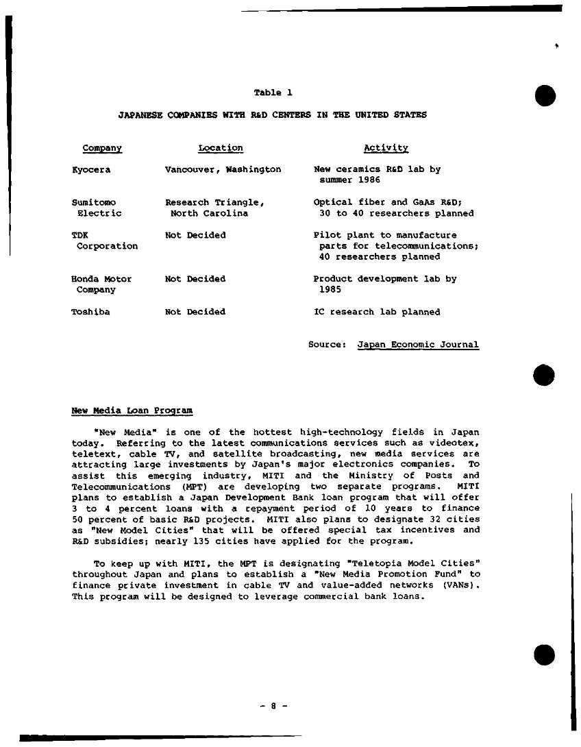
Table 1
JAPANESE COMPANIES WITH R&D CENTERS IN THE UNITED STATES
Company
Kyocera
Location
Vancouver, Washington
Activity
New ceramics R&D lab by summer 1986
Sumitomo Electric
TDK Corporation
Honda Motor Company
Toshiba
Research Triangle, North Carolina
Not Decided
Not Decided
Not Decided
Optical fiber and GaAs R&D; 30 to 40 researchers planned
Pilot plant to manufacture parts for telecommunications; 40 researchers planned
Product development lab by 1985
IC research lab planned
Source: Japan Economic Journal
New Media Loan Program
"New Media" is one of the hottest high-technology fields in Japan today. Referring to the latest communications services such as videotex, teletext, cable TV, and satellite broadcasting, new media services are attracting large investments by Japan's major electronics companies. To assist this emerging industry, MITI and the Ministry of Posts and Telecommunications (MPT) are developing two separate programs. MITI plans to establish a Japan Development Bank loan program that will offer 3 to 4 percent loans with a repayment period of 10 years to finance 50 percent of basic R&D projects. MITI also plans to designate 32 cities as "New Model Cities" that will be offered special tax incentives and R&D subsidies; nearly 135 cities have applied for the program.
To keep up with MITI, the MPT is designating "Teletopia Model Cities" throughout Japan and plans to establish a "New Media Promotion Fund" to finance private investment in cable TV and value-added networks (VANs). This program will be designed to leverage commercial bank loans.
- 8 -
GOVEBMMENT R&D ACTIVITIES
Sale of MITI Patents Proposed
Due to budget limits, MITI announced in July that it plans to sell patent rights to private industry in order to produce new revenues. Since Its founding in 1949, MITI has been granted more than 11,000 patents. Profits will be used to fund operating expenses, which are down 10 percent from fiscal 1983, and investment in MITI laboratories, which is down 5 percent. The proposal is being reviewed by the Ministry of Finance, but prospects look good because of growing calls for selling government patents to reduce the budget deficit. In mid-October, the Japan Industrial Technology Promotion Association sent a mission to the United States and Canada to sell 30 MITI-owned patents in new ceramics, electronics, mechatronics, and biotechnology. The mission will visit Montreal, San Antonio, Chicago, and various research institutes. To date, only 590 of the 11,000 patents have been licensed to private firms. MITI has not announced whether it will license its patents for advanced semiconductor technologies, such as GaAs, Josephson junctions, three-dimensional ICs, and optoelectronics.
100-Megabit DRAM Project Proposed
In March 1984, a group of Japanese semiconductor makers and university researchers headed by Professor Shoji Tanaka of Tokyo University proposed a $210 million, five-year project to develop a 100-megabit dynamic RAM using 0.25-micron geometries. Although no decision has been made yet, MITI officials are discussing the proposal. DATAQUEST believes that MITI officials are seeking a program to compete with Nippon Telegraph and Telephone (NTT), which is developing 4Mb and 16Mb DRAMS for its Information Network System (INS), a nationwide telecoimnunications network of fiber optics and satellites. Professor Tanaka was coordinator of the well-known VLSI Project (1976-1980), which developed the 64K DRAM as well as process equipment that is beginning to enter the U.S. market.
Opening of MITI Laboratories
In early August, MITI launched a new joint research system designed to promote joint government-industry research. Beginning in fiscal 1985, MITI's nine research facilities at the Tsukuba Science City, which is located 30 miles northeast of Tokyo, will accept researchers from Japanese companies and allow them to bring in private equipment as well as to take advantage of MITI's highly sophisticated equipment. This is a major policy shift, since private researchers were prohibited from entering MITI labs in the past. Immediately scheduled for joint R&D ventures are radiation application technologies using electron accumulation equipment at MITI's Electrotechnical Laboratory and new materials development at the National Chemical Laboratory for Industry. The new R&D system is designed to reduce the financial and technological
- 9 -
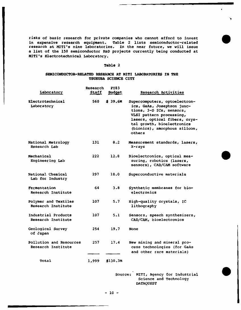
risks of basic research for private companies who cannot afford to invest in expensive research equipment. Table 2 lists semiconductor-related research at MITI's nine laboratories. In the near future, we will issue a list of the 150 semiconductor R&D projects currently being conducted at MITI's Electrotechnical Laboratory.
Table 2
SEMICONDUCTOR-RELATED RESEARCH AT MITI LABORATORIES IN THE TSOKUBA SCIENCE CITY
Laboratory Research FYS3 Staff Budget Research Activities
Electrotechnical Laboratory
560 $ 39,6M Supercomputers, optoelectronics, GaAs, Josephson junctions, 3-D ICs, sensors, VLSI pattern processing, lasers, optical fibers, crystal growth, bioelectronics (bionics), amorphous silicon. Others
National Metrology Research Lab
131 8.2 Measurement standards, lasers. X-rays
Mechanical Engineering Lab
222 12.8 Bioelectronics, optical measuring, robotics (lasers, sensors), CAD/CAM software
National Chemical Lab for Industry
297 18.0 Superconductive materials
Fermentation Research Institute
64 3.8 Synthetic membranes for bioelectronics
Polymer and Textiles Research Institute
107 5.7 High-quality crystals, IC lithography
Industrial Products Research Institute
107 5.1 Sensors, speech synthesizers, CAD/CAM, bioelectronics
Geological Survey of Japan
254 19.7 None
P o l l u t i o n and Resources Research I n s t i t u t e
257 17.4 New mining and mineral process technologies (for GaAs and Other rare materials)
Total 1,999 $130.3M
Source: MITI, Agency for Industrial Science and Technology DATAQUEST
- 10 -
New High-Technology Oniverslty
In July 1984, MITI announced that it will support development of a new private university in the Tsukuba Science City to train high-technology engineers and researchers. Keiichi Oshima, professor at Tokyo University, and Jiro Ushio, president of Ushio Inc., presented the plan to MITI vice minister Keiichi Konaga, citing a recent study by the National Institute for Research Advancement showing that Japanese engineering departments are not graduating enough students in semiconductors, biotechnology, and other high-technology fields. Tentatively called the Institute of High Technology, the new university will aim at supplying more trained researchers to private industry. Although the Ministry of Education is encouraging joint research between universities and private industry, Japanese universities are still weak in training competent researchers.
Mext-Generation Semiconductor EguJEanent Project
In July, MITI announced that it will spend $125 million (¥30 billion) over the next eight years to develop new process technologies for semiconductors, precision machine tools, and new compound materials. This project will focus on semiconductor equipment required for the next-generation semiconductor devices being developed by other MITI projects, such as three-dimensional ICs, gallium arsenide (GaAs) digital ICs, and bioelectronic ICs. DATAQUEST observes that MITI is emphasizing new semiconductor process equipment that is not available in the West. The New Semiconductor Functions Element Project, for example, has brought in Canon, Mitsui, and Seiko Instrument to develop semiconductor test equipment for three-dimensional ICs, superlattice devices, and hardened ICs. This new project is part of Japanese industry's overall thrust into semiconductor equipment. DATAQUEST observes that 714 of the 1,911 semiconductor-related patents granted were for process equipment.
PLANT SITING AND EXPANSION
Technopolis Program
MITI's key strategy for the 1980s and 1990s is its Technopolis Concept, an ambitious plan to create 19 high-technology cities patterned after Silicon Valley. The new cities will have populations of 200,000 and will feature research parks combining universities, corporate laboratories, and venture businesses. In February 1984, MITI formally designated nine cities for R&D funding, 7.3 percent Japan Development Bank loans, and tax subsidies. These cities are Nagaoka, Toyama, Hamamatsu, Hiroshima, Kumamoto, Ube, Oita, Kaghoshima, and Miyazaki, as shown in Figure 2. Recently, MITI also designated Okayama, Utsunomiya, and Kurume-Tosu, and plans to establish "Techno-Marts" on an experimental basis in Hamamatsu and Kumamoto to promote trade in technical information and patents. MITI estimates that each of the Technopoli will spend about
- 11 -
$2 b i l l i o n to $2.5 b i l l i on on new infras t ructure (roads, housing, research parks, u n i v e r s i t i e s ) , making the Technopolis Concept a $40 b i l l i o n to $50 b i l l i on investment. The c i t i e s have already formed jo in t R&D programs and technology centers to upgrade the i r research c a p a b i l i t i e s . DATAQUEST researchers have v i s i t ed the top 11 Technopoli, which wi l l be described in a book to be published next spr ing .
Figure 2
JAPAN'S 19 TECHNOPOLIS SITES
Trrfe •' -W^^ '•• /"i'-^ " L.Ti^ >-r,-J:.., r ,., /t^^miitr"'*-^"-
Wfi^.-^ ^'^ ^ 4- y^ .*r /--vikMVsiu^
1fcZ!^!Z.^T«4i MtM
ii VvG"'—"
f
T«chnopola Tenninology
• Mother city: txistoif dlkf of • 200,000 or mott popubtion to provide dfjr convcoitncet to udmopolitaas
• TtchnopoUszofic: u n in which a Itchnopotb wiUbcbuili
• Ttchnopolit center: the tcchnopolb' mein pbu where its headquarieia. cenfeicnce hilU. tndc fair ludiiunt ind other civic ^ildinrs chif ter
• Conpkxcf: Hpanie diitricu fat the technopolis io«c to hou« limiUr tjrpet of buddings (e.g. an indunrul complex •ccommodatini ficloriei, wvehouKS and other buiinen faciUtics)
Source: Ministry of International Trade and Industry
" 12 -
# Matchmaking Service for Foreign Companies
To promote plant siting and investment by foreign companies and to reduce trade friction, MITI established the Foreign Investment Servicing Office in May 1984. Working through the overseas offices of the Japan External Trade Organization (JETRO) and the Japanese Chamber of Commerce, MITI will help foceign companies find Japanese partners or subcontractors and will provide consulting services to firms planning to do business in Japan or with Japanese partners.
In response to American demands for access to MITI's Industrial Structure Council policy-making meetings, MITI began advisory meetings with the American Chamber of Commerce in Japan (ACCJ) in September. The talks will focus on MITI trade policies and U.S. complaints and requests, especially in high-technology areas such as semiconductor trade, VANs, and software protection. The ACCJ is led by Robert Sharp, vice president and deputy manager of the Tokyo branch of Manufacturers Hanover Trust Co; has 22 active committees; and consists of 540 American firms and 1,300 individual members.
Sheridan Tatsuno
- 13 -
Dataquest JAPANESE RESEARCH NEWSLETTER
EIEJ Codei Newsletters
PRESTOWITZ OUTLINES U.S.-JAPAN HIGH-TECHNOLOGY ISSUES
SUMMARY
Clyde Prestowitz, cochairman of the U.S.-Japan High-Technology Trade Commission and assistant secretary of international economic policy in the Department of Commerce, recently discussed key high-technology issues with industry leaders and scholars at Stanford University's U.S.-Japan Asia Forum. A top negotiator for the Reagan administration, Mr. Prestowitz described his efforts to open the Japanese market to non-Japanese investment, research, and manufacturing companies. His discussion focused on these key issues:
.•i Unequal access to research facilities
* Patent processing
9 NTT procurement
• Software protection
o Telecommunications legislation
ACCESS TO RESEARCH FACILITIES
Unlike the United States, Mr. Prestowitz believes that Japan is relatively closed to non-Japanese researchers and scientists. Currently, there are 200 Japanese researchers at the U.S. National Institute of Health, 10 at the Lawrence Livermore Laboratories, and hundreds of graduate students and professors studying and teaching in U.S. universities. Moreover, Japanese researchers make maximum use of the National Technical Information Service (NTIS), providing it with significant revenues. On the other hand, non-Japanese professors are not given tenure in Japanese universities, and there are few non-Japanese researchers in Japanese government research projects. Equal access is still a long way off, but Mr. Prestowitz noted that it is gradually changing. Recently, Nippon Telegraph and Telephone (NTT) and the National Bureau of Standards (NBS) agreed to exchange researchers.
© 1984 Dataquest Incorporated Aug. 9 ed.-Reproduction Prohibited
The content of this report represents our interpretaion and analysis of information generally available to the public or released by responsible individuals in the subject companies, but Is not guaranteed as to accuracy or completeness. It does not contain material provided to us In conlidence by our clients Individual companies repoled on and analyzed by DATAQUEST. may be clients of this and/or other DATAOUEST services This information is not lurnished In connection with a sale or offer to sell securities or in connection with the solicitation o! an oner to buy securities. Tnis firm ana its parent and/or their officers, stocicholders. or members ol their families mav from time to time, have a long or short position in the securities mentioned and may sell or buy such securities
Azabu Heights, Suite 711, 1-5-10 Roppongi, Minato-ku, Tokyo 106, Japan 1290 Bidder Park Drive / San Jose, CA 95131 / (408) 971-9000 / Telex 171973
PATENT PROCESSING
Japan's patent processing system puts U.S. companies at a serious competitive disadvantage. Whereas the U.S. Patent Office usually grants patent rights after 2 to 3 years (a period that will be reduced to 18 months due to the Patent Office's automation program), the Japanese Patent Office takes at least 6 to 7 years. In some cases, it has taken up to 12 to 14 years for important patents. The most controversial case is Corning Glass's fiber optic patent application, which was submitted in 1968. Although the United States granted the patent in 1971 and Europe in 1973, Japan has still not granted patent rights. Corning argues that this delay allowed major Japanese manufacturers to infringe on its patent rights, putting it at a disadvantage in NTT's fiber optic procurement program. Vice Minister Wakasugi is trying to automate the Patent Office and reduce piracy, but this effort will take at least several years.
NTT PROCUREMENT
Whereas Japan exported more than $1 billion in telecommunications equipment to the United States in 1983, U.S. companies exported only $140 million to Japan, despite the competitiveness of their equipment. Mr. Prestowitz believes that the major reasons for this imbalance are the openness of the U.S. market since AT&T divestiture, and NTT's previously "closed" procurement practices. Although NTT now has agreed to open its procurement practices and to establish branch offices in the United States, Mr. Prestowitz observed that NTT occasionally lapses into favoring the "NTT family"; he cited NTT's policy not to buy U.S. communication satellites as a case in point. Only after talks with Mr. Prestowitz did NTT President Shinto reverse that policy.
DATAQUEST believes that NTT procurement is one of the most significant high-technology markets in Japan. In fiscal 1984, NTT plans to procure $1.65 billion of fiber optic cable and digital switching systems during the next 20-years for use in its $120 billion Information Network System (INS).
SOFTWARE PROTECTION
The major controversy in U.S.-Japan high-technology relations is software protection. MITI believes that Japan is behind the United States in software and needs to protect this "infant industry." The Ministry of Education traditionally has held the legal authority to administer copyright law, but MITI argues that software is an "economic good" requiring patent protection, not intellectual property that should be accorded the same copyright protection as books and movies. (For more information on this subject, see our EIEJ Research Newsletter, "MITI Bows to U.S. Demand for Software Copyright Protection," April 12 1984.) Late last year, MITI introduced the Software Patent Bill. After strong protest from the U.S. Embassy and Mr. Prestowitz, and much debate with the Cultural Agency of the Ministry of Education, MITI quietly withdrew the bill.
- 2 -
Mr. Prestowitz noted that Japan and the United States are both signatories to the Berne Convention, an international copyright.pact, and argued that a copyright protects the expression of an idea, not necessarily the idea itself. The basic concepts between software data bases, for example, are often similar, but copyright law nevertheless protects their unique features.
TELECC»lMUNICATIONS BILL
The U.S. Embassy opposed the Telecommunications Bill prepared by the Ministry of Posts and Telecommunications (MPT), which would have restricted non-Japanese ownership to 20 percent in value-added network (VAN) services. Keidanren (Federation of Economic Organizations), a private, nonprofit organization comprising 110 major industry associations and the largest 812 corporations, argued that MPT needs to protect "its little babies," such as NEC, Hitachi, and other telecommunications manufacturers. This bill will be reintroduced later this year, along with the bill to divest NTT.
Sheridan Tatsuno
- 3 -
Dataquest JAPANESE RESEARCH NEWSLETTER
EIEJ Code: Newsle t te rs
WORLDWIDE TECHNICAL MEETINGS
Because of the need to be aware of important b u s i n e s s / t e c h n i c a l meetings throughout the world, DATAQUEST has compiled a calendar cover ing major meetings of importance t o a l l JSIS c l i e n t s .
We have researched and a r e now making a v a i l a b l e to you a ca lendar for the second hal f of 1984. The calendar l i s t s meeting d a t e s , t i t l e s , l o c a t i o n s , and addresses for i n q u i r i e s . We are c u r r e n t l y research ing the major events for 1985, and w i l l send t h i s calendar out l a t e r in the y e a r .
Gene Nor re t t
© 1984 Dataquest Incorporated July 18 ed. -Reproduct ion Proh ib i t ed
The content of this report represents our interpretaion and analysis of information generally available to the public or released by responsible individuals in the subject companies, but is not guaranteed as to accuracy or completeness. It does not contain material provided to us in co""dence by our clients Individual comoanies reoorted on and analyzed by DATAQUEST, may be clients of this and/or other DATAQUEST services This information is not furnished in connection with a sale or otter to sell securities or in connection with the solicitation of an offer to Duy securities This firm and its parent and/or their officers, stockholders, or members ol their families may, from time to time, have a long or short position in the securities mentioned and may sell or buy such securities
Azabu Heights, Suite 711, 1-5-10 Roppongi, Minato-ku, Tokyo 106, Japan 1290 Ridder Park Drive / San Jose, CA 95131 / (408) 971-9000 / Telex 171973
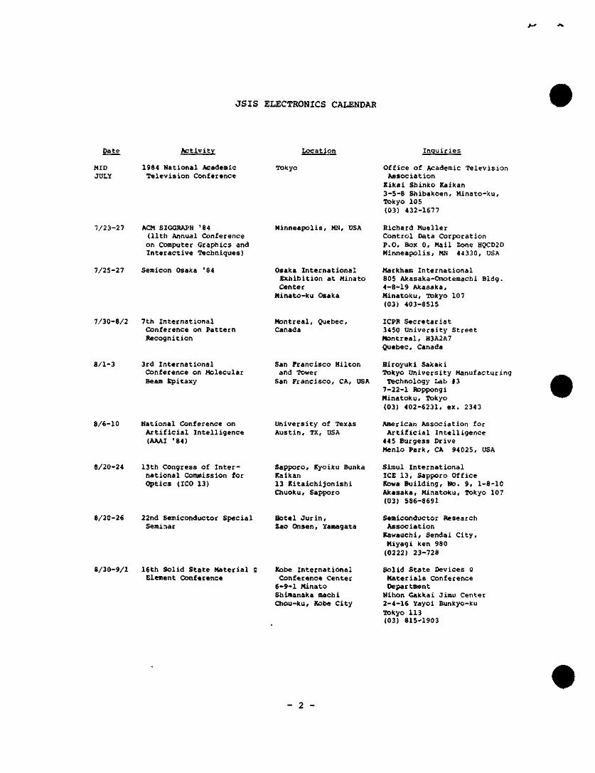
JSIS ELECTRONICS CALENDAR
Date Activity
MID 1984 National Academic JULY Television Conference
Location
Tokyo
Inquiries
Office of Academic Television Association Kikai Shinko ICaikan 3-5-8 Shibakoen, Minato-ku, Tokyo 105 (03) 432-1677
7/23-27 ACM SIGGRAPH "84 (11th Annual Conference on computer Graphics and Interactive Techniques)
Minneapolis, MN, USA Richard Mueller Control Data Corporation P.O. Box 0, Mail Zone HQCD2D Minneapolis, MN 44330, USA
7/25-27 Semicon Osaka '84 Osaka International Exhibition at Minato Center
Minato-ku Osaka
Markham International 805 Akasaka-Omotemachi Bldg. 4-8-19 Akasaka, Minatoku, Tokyo 107 (03) 403-8515
7/30-8/2 7th International Conference on Pattern Recognition
Montreal, Quebec, Canada
ICPR Secretariat 3450 University Street Montreal, H3A2A7 Quebec, Canada
8/1-3 3rd International Conference on Molecular Beam Epitaxy
San Francisco Hilton and Tower San Francisco, CA, USA
Hiroyuki Sakaki Tokyo University Manufacturing Technology Lab #3 7-22-1 Roppongi Minatoku, Tokyo (03) 402-6231, ex. 2343
8/6-10 National Conference on Artificial Intelligence (AAAI '84)
University of Texas Austin, TX, USA
American Association for Artificial Intelligence 44S Burgess Drive Menlo Park, CA 94025, USA
8/20-24 13th Congress of International Commission for Optics (ICO 13)
Sapporo, Kyoiku Bunka Kaikan 13 Kitaichijonishi Chuoku, Sapporo
Simul International ICE 13, Sapporo Office Kowa Building, No. 9, 1-8-10 Akasaka, Minatoku, Tokyo 107 (03) 586-8691
8/20-26 22nd Semiconductor Special Seminar
Hotel Jurln, Zao Onsen, Yamagata
Semiconductor Research Association Kawauchl, Sendai City, Miyagi ken 980 (0222) 23-728
8/30-9/1 16th Solid State Material C Element Conference
Itobe International Conference Center 6-9-1 Minato Shimanaka machi Chou-ku, Kobe City
Solid State Devices 0 Materials Conference Department
Nihon Gakkai Jimu Center 2-4-16 Yayoi Bunkyo-ku Tokyo 113 (03) 815-1903
- 2 -
9/10-12 Electronics and Aerospace Systems Conference (EASCON '84)
Shoreham Hotel Washington, D.C, USA
William E. Bearry Manager, Government Marketing Satellite Business Systems 8003 Westpark Drive McLean, VA 22102, USA
9/16-20 COMPCON Fall '84 Arlington, VA, USA COMPCON Fall '84 P.O. Box 639 Silver Spring, MD 20901, USA
9/17-19 International Microelectronics Symposium (ISHM '84)
Dallas, TX, USA Hisao Hirabayashi, ISHM Japan, 5-635 Hanakoganei, Kodaira City,
Tokyo, 187 (0424) 67-7602
9/17-21 U.S. Laboratory Automation Exhibit at Tokyo
USA Trade Center World Import Mart 7th Floor 3-1-3 Higashi Ikebukuro Toshima-ku, Tokyo
us Trade Center World Import Mart, 7th Floor 3-1-3 Higashi Ikebukuru Toshima-ku Tokyo 170 (03) 987-2441
9 /20 -22 Nepcon Osaka "84 Osakajo Hall 37 Osakajo, Higashi-ku Osaka, Japan
CEG Japan Shinjuku Mitsui Building No. 2 3-2-11 Nishi-Shinjuku, 160 (03) 349-8501
9/21-25 10th International Broadcasting Convention (IBC '84)
Brighton Metropole Conference 0 Exhibition Centre Brighton, U.K.
Secretary IBC Technical Programme Committee IBC Secretariat lEE Savoy Place London WC2R OBL U.K.
9/24-25 U.S. Laboratory Automation Exhibit at Osaka
American Merchandise Display Osaka Sankei Kaikan Bldg. 2-4-9 Uraeda Kita-ku, Osaka
us Trade Center World Import Mart 7th Floor, 3-1-3 Higashi Ikebukuro, Toshima-ku, Tokyo 170 (03) 987-2441
9/26-28 11th International Symposium on Gallium Arsenide and Related Compounds
Biarritz, France Takashi Atoda Tokyo University Engineering Department Boarder Domain Research
4-6-1 Koraaba, Meguro-Ku Tokyo, 153 (03) 485-3111, ex. 362
9/26-29 Data Show '84 Tokyo International Exhibition Center Harumi, Chuo-ku, Tokyo
Japan Electronics Industry Promotional Association Data Show '84 Office Kikai Shinko Kaikan 3-5-8 Shiba Koen, Minato-ku, Tokyo 105 (03) 434-8211, ex. 352
- 3
10/1-5 International Symposium on Subscriber Lines and Service (ISSLS '84)
Nice, France Masaki Koyama, NTT Yokosuka Telecommunication Lat 1-2356 Take, Yokosuka City Kanagawa-ken, 238, (0468) 59-3180
10/2-4 Software Show '84 Shinjuku NS Building 204 Nishi-shinjuku Shinjuku-ku, Tokyo
Software Distribution Promotion Center Yusei Gojokai Konpira B ldg . 1-14-1 Toranomon, Minato-ku, Tokyo 105 (03) 591-2440
10/4-9 1984 Electronics Show Tokyo International Exhibition Center
Harumi, Chuo-ku, Tokyo
Japan Electronics Show Assoc. Tosho Bldg. 3-2-2 Marunouchi Chiyoda-ku, Tokyo 100 (03) 284-1051
10/16-18 Environmental Electromagnetic Engineering (EMC) International Symposium
Hotel Pacific, Tokyo 3-13-3 Takanawa, Minato-ku, Tokyo
Ai Takagi Tohoku University Telecommunications Dept. Aoba Aza, Aramaki, Sendai City,
Miyagi-ken, 980 (0222) 22-1800, ex. 4266
10/16-18 International Test Conference (Cherry Hill '84)
Franklin Plaza Hotel Philadelphia, PA, USA
Harry Hayman P.O. Box 639 Silver Spring, MD 20901, USA
10/16-19 •84 Japan Electronic Test Exhibition
Kagaku Gijutsu Kan 2-1 Kitanomarukoen Chiyoda-ku, Tokyo
Japan Electronic Test Industry Association 1-9-10 Toranomon Minato-ku, Tokyo 105 (03) 502-0601
10/23-25 International Broadcast Equipment Exhibition
Tokyo Distribution Center 6-1-1 Heiwajima Ota-ku, Tokyo
Japan Electronic Show Assoc. Tosho Building 3-2-2 Marunouchi, Chiyoda-ku Tokyo 100 (03) 284-1051
10/30-11/1
Western Electronic Show and Convention (WESCON '84)
Los Angeles, CA, USA Dale Litherland Electronic Convention, Inc. 8110 Airport Boulevard Los Angeles, CA 90045, USA
10/30- 7th International 11/2 Conference on Computer
communication (ICCC '84)
Sydney Opera House and Centre Point Sydney, Australia
Hiroshi Yoshida, NTT Musashino Telecommunication Lab Bucket Switching Research Lab 3-9-11 Midoricho, Musashino City, Tokyo 180 (0422) 59-4220
- 4 -
10/30-11/2
'84 Optoelectronics Show Tokyo Distribution Center 6-1-1 Heiwajima Ota-ku, Tokyo
Optical Industry Technology Association
Mori Bldg. No. 20, 2-7-4 Nishi-Shinbashi, Minato-ku, Tokyo 105 (03) 508-2091
10/31-11/2
4th International Conference on Perrites
Sheraton Palace Hotel San Francisco, CA, USA
Mitsuo Sugimoto Saitama University Electronic Engineering Department 255 Shimookubo, Urawa City Saitama-ken, 338 (0488) 52-2111, ex. 2263
11/5-9 COMPSAC '84 Chicago, XL, USA COMPSAC '84 P.O. Box 639 Silver Spring, MD 20901 USA
11/5-9 Microwave System Component Exhibit
US Trade Center World Import Mart 7th Floor 3-1-3 Higashi Ikebukuro
Toshima-ku, Tokyo
US Trade Center World Import Mart, 7th Floor 3-1-3 Higashi Ikebukuro Toshima-ku, Tokyo 170 (03) 987-2441
11/6-9 International Conference on 5th Generation Computer Systems (FGCS '84)
Keio Plaza Hotel Nishi-shinjuku, Shinjuku-ku, Tokyo
New Generation Computer Technology Development Organization (ICOT)
Mita Kokusai Bldg. 1-4-28 Mita Minato-ku, Tokyo 108 (03) 456-2511
11/7-11 Electronica '84 Munich, Federal Republic of C^rmany
Gerald G. ICallman ICallman Associates 5 Maple Court Ridgewood, NJ 07450, USA
11/11-14 International Telecommunications Energy Conference (INTELEC '84)
New Orleans Hilton New Orleans, LA, USA
James M. Fletcher Western Electric Co. Gateway II Newark, NJ 07102, USA
11/13-16 1st Solar Electric Generation International Conference
Kobe International Conference Center 6-9-1 Minatoshimanaka Chuo-ku, Kobe
Taneo Nishino Osaka University Basic Engineering Department 1-1 Machikaneyamacho, Itoyonaka City 560 (06) 844-1151, ex. 4586-8
11/20-23 1st Electronic Equipment Exhibition (PRONIC '84)
11/25-29 Global Telecommunications Conference (GLOBECOM '84)
Porte de Versailles Exhibition Center Paris, France
Atlanta Hilton Atlanta, GA, USA
France Exhib i t ion A s s o c , Japan O f f i ce
5 -5 -1 Itoppongi, Minato-ku Tokyo 106 (03) 405-0171
Allan H. Cherin Bell Labs 200 N.E. Expressway Norcross, GA 30071, USA
12/3-5 SEMICON Japan '84 Tokyo International Exhibition Center
Harumi Chuo-ku, Tokyo
Markhan International SEMICON Japan Office 805 Akasaka-omotemachi Bldg. 4-8-19 Akasaka, Minato-ku, Tokyo 107 (03) 403-8515
- 5 -
^ s T ^ Dataquest RESEARCH BULLETIN 1
EIEJ Code: N e w s l e t t e r
ANELVA INTRODUCES GALLII3H ARSENIDE WAFER PROCESSING EQUIPMENT
\
s
I- -11 1
^B
Anelva Corporation, a major semiconductor equipment maker in Japan, announced on July 5 that it has developed molecular beam epitaxy (MBE) equipment capable of processing 3-inch gallium arsenide (GaAs) wafers. The equipment, which will be priced between ¥130 million and ¥140 million ($565,000 and $609,000), includes two machines:
• A substrate conveyor machine capable of handling six wafers at a time (MBE-831)
• Substrate revolving equipment to improve the uniformity of the thick-film deposition (MBE-832)
The equipment can be used to produce III-V and II-Vl compound semiconductors, such as GaAs metal-semiconductor field-effect transistors (MESFETs), high-electron mobility transistors (HEMTs), semiconductor lasers, and high-performance bipolar ICs. At present, the equipment is being used for research and trial production, but will soon be introduced for commercial production.
Anelva specializes in three types of semiconductor equipment: analytical equipment, vacuum instruments (sputtering systems, reactive ion-etching systems, plasma CVD systems, and MBE systems), and thin-film deposition equipment. The company was formed in October 1967 as a joint venture between NEC Corporation and Varian U.S.A., but Varian subsequently sold its shares to NEC Corporation. In recent years, Anelva has introduced advanced in-line sputtering (ILC-1012) and dry-etching (ILD-4002) equipment. Its development of GaAs wafer processing equipment marks the company's move into next-generation semiconductor equipment.
As shown in Table 1, the company recently completed its new Fuji plant in Yamanashi Prefecture to expand production. In addition to its Japanese facilities, Anelva has a sales office in San Jose, California.
© 1984 Dataquest Incorporated July 17 ed.-Reproduction Prohibited
Tne content ot tttis report tepfesents out interpretation
oro. i f lpn 10 us 1" coni iaence by our r t ients tnrjivcluat co
, n o . n a t , s i , „ , , n
npan.es reOOrted
m and its patent a
n a
n o r
a t
n r l
. r ,
on general
i naWiedb
hen ol l icer
y available lo the
DATAQUEST ma
s stocl<holoers or
utilic or released tiy
be chentso l Ihis a
m e m b e - s o l t h e i . l a
respon
d'or ot
r ^ . i es r
sible individuals in ihe subIec
her DATAQUEST services Th
nay trom jime to time nave a
I companies bui is n
s information is nol t
ong or snun uubuu,t
Ot guaran
jrnished
e e d a s l o a c c .
— • = - ^ = " - ' -
t h
, •
o-comple leness
s a i e o - o t l e r t o s e
„..J , . „ , E2" -" b'
It does not conla i
I securit ies or in c
, , t , . - h . . . t , t . t P .
T maienai Dnnection
Dataquest Incorporated, A Subsidiary of A.C. Nielsen Company / 1290 Bidder Park Drive / San Jose, CA 95131 / (408) 971-9000 / Telex 171973
Table 1
ANELVA PRODUCTION FACILITIES
Location
Main Plant (Fuchu) Higashi Plant (Fuchu) Fuji Plant (Yamanashi Prefecture)
Total Production
Date
October 1968 April 1980
April 1983
Floor Area (Square Meters)
9,461 815
7,100
17,376
Number of Employees*
532 13
116
661
•Excludes 39 administrative personnel
Source: Anelva Corporation
DATAQUEST believes that Anelva's recent announcement reflects the growing commercialization of GaAs devices in Japan. As noted in our 10 February 1984 Research Newsletter entitled "Gallium Arsenide Production Takes Off in Japan," we estimate that total Japanese production of GaAs devices will be ¥30.0 billion ($125 million) in 1984, up 41 percent from 1983. GaAs MESFETs being used in cable TV converters, mobile phones, and broadcast satellite amplifiers will account for 44 percent of total Japanese production, while semiconductor lasers used in digital audio disk (DAD) players, telecommunications, and optical disk files will represent 12 percent of the total. The availability of GaAs wafer processing equipment will be crucial to semiconductor makers for improving wafer yields and quality.
Sheridan Tatsuno
- 2 -
EIEJ Code: Newsle t te rs
MANDFACTORING EQUIPMENT I N D U S T R Y -GROWTH OF JAPAN AND REST OF WORLD
Semicon West held i t s annual t r a d e show May 21 through May 25, 1984. The show included p r e s e n t a t i o n s by members of DATAQUEST's Semiconductor Group. Gene N o r r e t t , Vice P re s iden t and D i r e c t o r , Japanese Semiconductor Indus t ry S e r v i c e , p resen ted an overview of the Manufacturing Equipment Industry—Growth of Japan and Rest of World.
The p r e s e n t a t i o n covered four major t o p i c s :
• Semiconductor and equipment t r ends in Japan
• P lan t s i t i n g of Japanese and Western equipment and m a t e r i a l s manufacturers
• J o i n t venture a c t i v i t i e s between the United S t a t e s and Japan
• Rest of world semiconductor market e s t ima te s with a focus on Korea
Gene Nor re t t
© 1984 Dataquest Incorpora ted June 8 ed.-Reproduct ion Proh ib i t ed
Tne content of ihis report represenis our InterD'etation and analysis o* information generally availatile to the oublic or released Dy responsib le indi«Iduals in the sub ieci companies bul is not guaranteed as lo accuracy or completeness It does not contain maienat
provided to us in conl idence by our cl ients Individual companies reported on and analyzed by DATAQUEST may tie cl ients o ' ihis and'or other DATAQUEST services This Information Is not furnished In connection witti a sale or ot 'er to sell securities or in connect ion
wi ih the sol ici tat ion ol an olfer to buy securI iIes This ' Irm and its parent and/or their officers siockholders or members of then families may trom l ime lo i ime have a long or short posIt ion in the securit ies mentioned and may sell or buy such securit ies
Dataquest Incorporated, A Subsidiary of A.C. Nielsen Company /1290 Bidder Park Drive / San Jose, CA 95131 / (408) 971-9000 / Telex 171973
Dataquest MAMtlFACTtmiMG EQUIPMENT INDUSTRY— GROWTH OF JAPAN AND REST OF WORLD
Gene Norrett Vice President cuid Director
Japanese Semiconductor Industry Service
Good morning, ladies and gentlemen.
Welcome again to DATAQUEST. As you have already heard, I am the director of the Japanese Semiconductor Industry Service with an American staff in San Jose and eut all-Japanese staff in Tokyo. This service was founded to provide research on Japanese semiconductor technology and equipment trends worldwide, with a focus on the explosive market in Japan. Our growing list of approximately 80 clients worldwide have been receiving approximately 60 pages of research material monthly since our inauguration in June 1983. Our conference next month, June 21, at the Tokyo American Club will have as its theme "East meets West in VLSI." I recommend that if any of you are planning on being in Tokyo at this time, you should attend this highly informative gathering. We will have Dr. Tanaka of Tokyo University and former director of the Japanese VLSI project as a guest speaker.
Today I will cover four main areas:
1. Semiconductor and equipment trends in Japan
2. Plant siting of Japanese and Western equipment and materials manufacturers
3. Joint venture activities between the United States and Japan
4. Rest of World semiconductor market estimates with a focus on Korea
Japanese Semiconductor Industry--Production Trends
The year 1984 is going to have the highest growth rate and be the most broadbased semiconductor industry expansion in the last eight years (see Slide 1) . Fueled by the explosive office automation equipment growth, specifically personal ccanputers, the 1984 production of all Japanese semiconductors will grow 38 percent in yen and 44 percent in dollars.
MOS devices will grow 55 percent and will grab a 48 percent share of all semiconductors produced, up 12 percentage points since 1980. It is these products that are driving the manufacturing equipment industry to produce state-of-the-art products.
So as to be able to provide our JSIS clients with a total industry perspective, we track the Japanese equipment and materials market and report periodically on its trends.
- 1 -O 1984 Dataquest Incorporated June 8 ed.-Reproduction Prohibited
Dataquest Incorporated, A Subsidiary of A.C. Nielsen Company /1290 Ridder Park Drive / San Jose, CA 95131 / (408) 971-9000 / Telex 171973
Shown in Slide 2 is our production revenue forecast for Japanese wafer processing, assembly, and testing equipment. The continuing battle between the steppers and projection aligners has furnished the semiconductor industry with a continuous flow of miracle-producing machines. In the wafer processing area, we have seen a compound annual growth of over 35 percent since 1980, with 1984 projected to increase 55 percent. Writing speeds, wafer-handling capabilities, and up-time reliability of the Japanese products are setting the standards for the world industry due to the requirements demanded by the dominent 64K and 256K dynamic RAM manufacturers such as Hitachi, NEC, and Fujitsu.
Because of the complexity of the VLSI devices, testing has become as important as wafer processing in the manufacturing process. Our forecast is for 40 percent growth in production revenues. In the past, the semiconductor manufacturer designed the circuit and then the testing manufacturer designed the equipment and programs needed to test it. The level of complexity of VLSI devices has clearly been reached today where designing for testability and, in fact, adding self-testing to the device design is more the rule than the exception.
The equipment manufacturers shown in Slide 3 represent the top 10 in Japan. I call your attention to the last column on this slide, compound growth rate. The average growth rate over the last four years was 32.6 percent compounded, a growth rate that has exceeded the semiconductor production growth rate over the same period by 27 percent. Nikon, Applied Materials-Japan, and Takeda-Riken have achieved the highest growth rates. Applied Materials' success in Japan is due, to a large extent, to its proximity to the customers and its aggressive marketing and service strategies. Currently, Applied Materials-Japan is planning to increase revenues by 60 percent in FY 1984, just slightly behind Nikon's explosive 63 percent.
Due to the decline in Japan's sunset industries such as steel, heavy electrical equipment, and mining, leading manufacturers in these fields have looked enviously at the sunrise semiconductor equipment industry. As part of our service to our clients, we continuously monitor the new players in this industry and I want to call your attention to some here today.
These manufacturers shown in Slides 4 and 5 have set their production and marketing plans on entering this industry for the first time, or are expanding horizontally. The names on this list should not be taken lightly. They have a heritage of success.
Japanese equipment and materials manufacturers (see Slide 6) as a group have been slower to establish manufacturing plants in the United States as compared to the Japanese semiconductor manufacturers. For example, our Japanese Semiconductor Industry Service factory data base contains a total of seven factories with two more in the planning phase. Our research has yielded only six companies shown here with only two of significance: Kyocera and Shinetsu Handotai. The $30 million SEH
- 2 -© 1984 Dataquest Incorporated June 8 ed.-Reproduction Prohibited
Dataquest Incorporated, A Subsidiary of A.C. Nielsen Company / 1290 Bidder Park Drive / San Jose, CA 95131 / (408) 971-9000 / Telex 171973
plant, near Vancouver, Washington, is the most modern, automated, totally integrated high-purity silicon wafer manufacturing facility in the world. This plant produces single crystal semiconductor-grade silicon ingates, and 4-, 5-, and 6-inch polished wafers.
In order to penetrate the rapidly growing Japanese semiconductor market, some forward thinking U.S. and European manufacturers have set up manufacturing facilities in Japan. These are shown in Slide 7. Materials Research Corporation (MRC), with headquarters in Orangeburg, New York, was the first U.S. manufacturer to set up a manufacturing plant in Japan. MRC opened its first plant in Kyushu in March 1984. The first manufactured products will be the waferline 11 cassette-to-cassette spluttering system. The Kyushu plant represented a $4 million investment for MRC. The project was also significant in that majority financing was provided by the Japanese Development Bank in the first-ever agreement with a primarily foreign-owned company.
In addition to MRC, our research shows six other companies that have opened plants, have plants under construction, or will open plants by the end of 1985. Our clients also have directed our attention to joint venture activities because of their strategic importance to the industry.
Just as in the semiconductor components industry, we have seen a rapid increase in joint ventures in the equipment industry over the last three years. Our joint venture data base shows ten joint ventures since January 1984, six in 1983, and ten in 1982. Here, on Slides 8 and 9, you can see who the bed partners are and for what technology.
The last area I want to cover this morning is the area known by many as Rest of the World (ROW).
As can be seen in Slide 10, the ROW semiconductor industry has increased 20 percent compounded over the past four years. The region is highly dependent on the consumer equipment markets that depressed the semiconductor industry in 1981 and 1982. We are seeing a rapid rise in this market currently, with consumption forecast to rise 34 percent. MOS memories and 8-bit MPUs and MCUs will see growth rates in excess of 60 percent for use in VTRs, telephones, and personal computers. Our service also covers this market in depth, with frequent reports on the growing markets in Korea, Hong Kong, Taiwan, and Singapore.
Speaking of Korea, we have seen a step function increase in the capital investment by leading Korean conglomerates such as Hyundai, Samsung, Gold Star, and Oae Wo.
Slide 11 shows the semiconductor sales and invest:ments by the top six Korean manufacturers. Please note the ratio of investment to sales in 1984—approximately 2:1. Taken together, we believe that these companies will invest $1.5 billion over the 1983 through 1988 period. These investments represent significant sales opportunities for equipment and materials manufacturers that support these Korean manufacturers in their quest for shoulder room in the world's semiconductor industry.
- 3 -© 1984 Dataquest Incorporated Jpne 8 ed.-Reproduction Prohibited
Dataquest Incorporated, A Subsidiary of A.C. Nielsen Company / 1290 Ridder Park Drive / San Jose, CA 95131 / (408) 971-9000 / Telex 171973
have n summacy, I want to call your attention to the major points that I raised this morning (see Slide 12):
Japanese semiconductor production up 38 percent
Semiconductor equipment revenues up 48 percent
Very high levels of joint venture activity
Some very large new players in the Japanese equipment and materials markets
ROW semiconductor and capital investments skyrocketing
Thank you for your attention.
- 4 -© 1984 Dataquest Incorporated June 8 ed.-Reproduction Prohibited
Dataquest Incorporated, A Subsidiary of A.C. Nielsen Company / 1290 Ridder Park Drive / San Jose, CA 95131 / (408) 971-9000 / Telex 171973
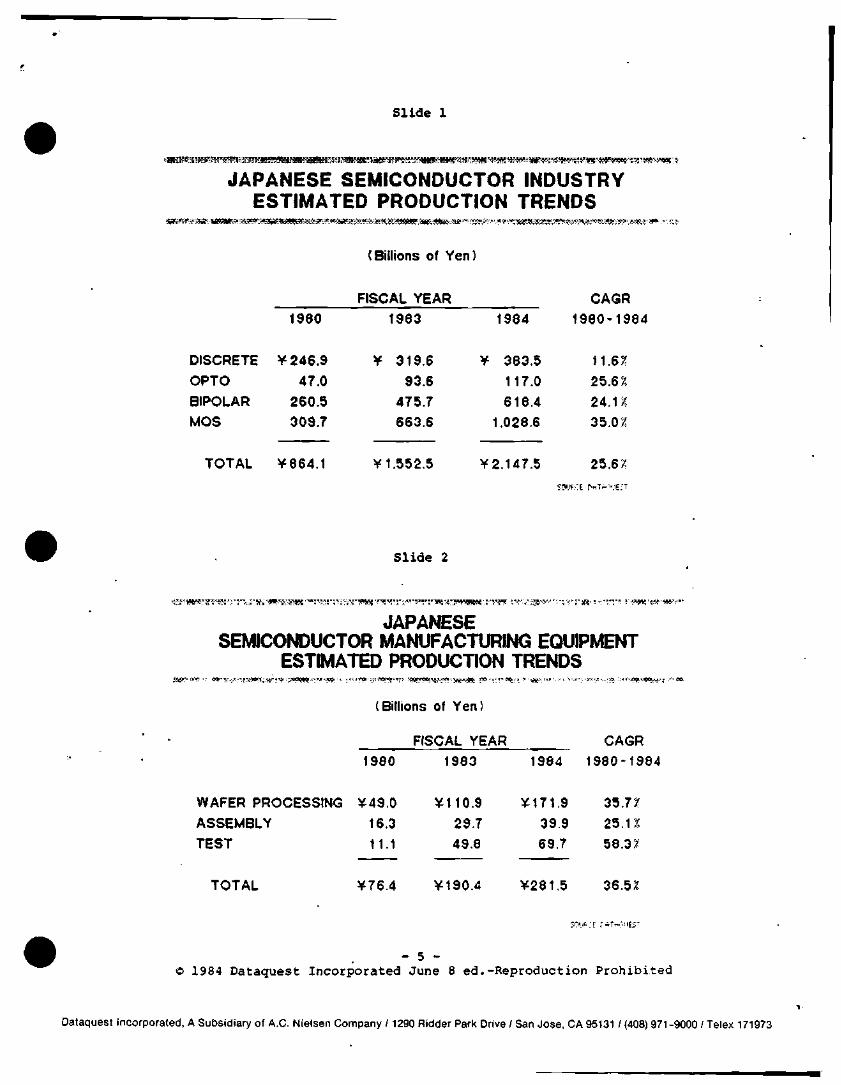
Slide 1
JAPANESE SEMICONDUCTOR INDUSTRY ESTIMATED PRODUCTION TRENDS
(Billions of Yen)
DISCRETE
OPTO
BIPOLAR
MOS
TOTAL
1980
¥246.9
47.0
260.5
309.7
¥864.1
FISCAL YEAR
1983
¥ 319.6
93.6
475.7
663.6
¥1.552.5
1984
¥ 383.5
117.0
618.4
1.028.6
¥2 .147.5
CAGR
1980-1984
11.65?
25.65;
24.1 ?
35.0)?
2^.67.
i"Oi.if::E rnTr-'-".lE;"T
S l ide 2
JAPANESE SEMICONDUCTOR MANUFACTURING EQUIPMENT
ESTIMATED PRODUCTION TRENDS
(Billions of Yen)
FISCAL YEAR CAGR
1980 1983 1984 1980-1984
WAFER PROCESSING ¥49.0 ¥110.9 ¥171.9 35.7?
ASSEMBLY 16.3 29.7 39.9 25.1%
TEST 11.1 49.8 69.7 58.3%
TOTAL ¥76.4 ¥190.4 ¥281.5 36.52
;OMs; r r ^iTt-OJ I E ;
- 5 -1984 Dataquest Incorporated June 8 ed.-Reproduction Prohibi ted
Dataquest incorporated, A Subsidiary of A.C. Nielsen Company / 1290 Ridder Park Drive / San Jose, CA 95131 / (408) 971-9000 / Telex 171973
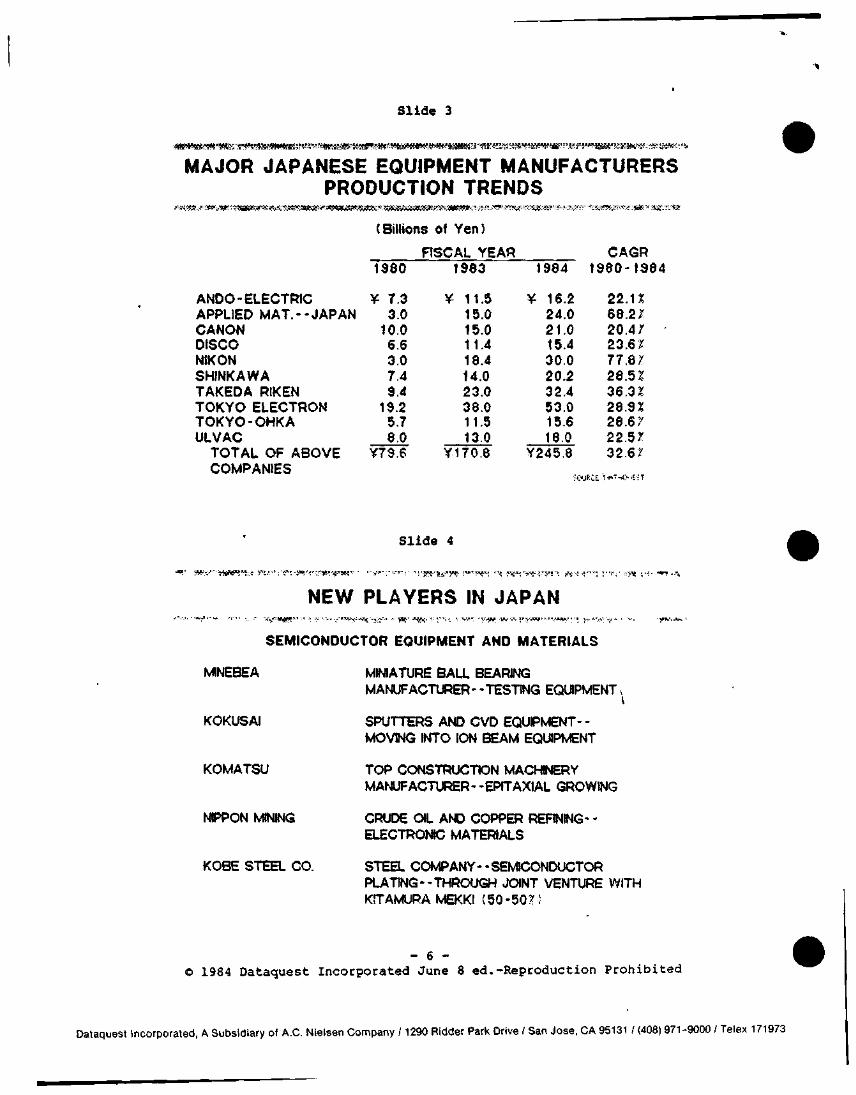
Sl ide 3
««w«fM'^is::i'r!««*:<*Iw«yfi;r«r5'w?Hi^^
MAJOR JAPANESE EQUIPMENT MANUFACTURERS PRODUCTION TRENDS
(Billions of Yen)
ANDO-ELECTRIC APPLIED MAT - -JAPAN CANON DISCO NIKON SHINKAWA TAKEDA RIKEN TOKYO ELECTRON TOKYO-OHKA ULVAC
TOTAL OF ABOVE COMPANIES
1980
¥ 7.3 3.0
10.0 6.6 3.0 7.4 9.4
19.2 5.7 8.0
Y79.6
FISCAL YEAR 1983
¥ 11.5 15.0 15.0 11.4 18.4 14.0 23.0 38.0 11.5 13.0
Y170.8
1984
¥ 16.2 24.0 21.0 15.4 30.0 20.2 32.4 53.0 15.6 18.0
Y245.8
CAGP 1980-1S
22.11 68.2X 20.47 23.6? 77.87 28.5^ 36.3^ 28.9X 28.67 22.57 32.67
•OUfiCE "[•«*-'C-'£;"T
S l ide 4
NEW PLAYERS IN JAPAN
SEMICONOUCTOR EQUIPMENT AND MATERIALS
MINEBEA
KOKUSAI
MINIATURE BALL BEARING MANUFACTURER--TESTING EQUIPMENT,
SPUTTERS AND CVD EQUPMENT- -MOVING INTO ION BEAM EQUIPMENT
I
KOMATSU TOP CONSTRUCTION MACHINERY MANUFACTURER--EPITAXIAL GROWING
NIPPON MINING CRUDE OIL AND COPPER RERNING-ELECTRONIC MATERIALS
KOBE STEEL CO. STEEL COMPANY--SEMICONDUCTOR PLATING--THROUGH JOINT VENTURE V/ITH KITAMURA MEKKi (50-50.7)
- 6 -© 1984 Dataquest Incorporated June 8 ed.-Reproduction Prohibited
Dataquest Incorporated, A Subsidiary of A.C. Nielsen Company / 1290 RIdder Park Drive / San Jose, CA 95131 / (408) 971-9000 / Telex 171973
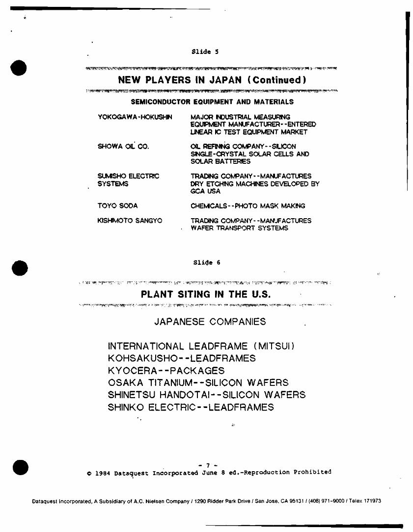
Sl ide 5
NEW PLAYERS IN JAPAN (Continued)
SEMICONDUCTOR EQUIPMENT AND MATERIALS
YOKOGA W A - HOKUSHIN
SHOWA OIL CO.
SUMISHO ELECTRIC SYSTEMS
TOYO SODA
KISHIMOTO SANGYO
MAJOR M>USTRIAL MEASURING EQUIPMEhfr MANUFACTURER--ENTERED UNEAR IC TEST EQUIPMENT MARKET
OIL REFINING COMPANY--SLICON SINGLE-CRYSTAL SOLAR CELLS AND SOLAR BATTERIES
TRADING COMPANY--MANUFACTURES DRY ETCHNG MACHINES DEVELOPED BY GCA USA
CHEMICALS--PHOTO MASK MAKING
TRADING COMPANY--MANUFACTURES WAFER TRANSPORT SYSTEMS
Sli(?e 6
', : j(: i 'wj: ^w^-i:^:;": '-:;;;; ' ;^?;" ;:;:•••*-•• ;;-<»»;^"' '"^rj-f- < ^ v :,^S«;^^'v^^-;-i^'<'^.-v:^?^:^^'"y!''rA;";r^ ^"Y^rV^^'^'^^i'^^r^: i-S:
PLANT SITING IN THE U.S.
JAPANESE COMPANIES
INTERNATIONAL LEADFRAME (MITSUI) KOHSAKUSHO- -LEADFRAMES KYOCERA- -PACKAGES OSAKA TITANIUM--SILICON WAFERS SHINETSU HANDOTAI--SILICON WAFERS SHINKO ELECTRIC--LEADFRAMES
- 7 © 1984 Dataquest Incorporated June 8 ed.-Reproduction Prohibited
Dataquest Incorporated, A Subsidiary of A.C. Nielsen Company / 1290 Ridder Park Drive / San Jose, CA 95131 / (408) 971-9000 / Telex 171973
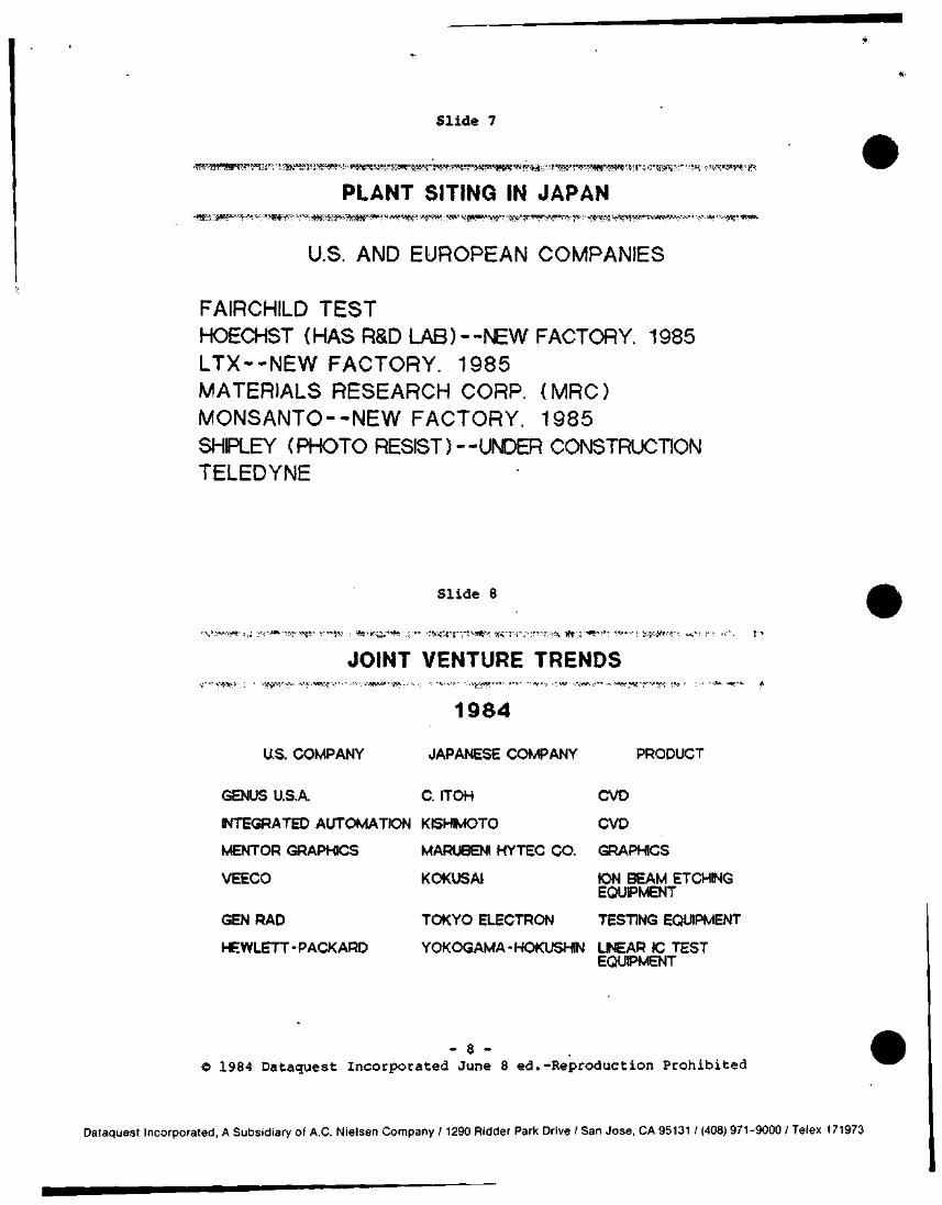
Slide 7
•S!?^^j!!W'?sp?^<?^v^;i3-^^;'V:^lHB*^i^"'»i^-^
PLANT SITING IN JAPAN 'l?ftt•^^':5!*y^^''i^i^•^.•">-;^Wi'^^t'^:i'Vi^ ^?Wf«! ••<JW tJ^Bjqaw^ . j^r . t^ . rvv^^s . i^^ '^ . f^ iir^'-ir.^, ^^lw-rr!.:^•»••v4•J»^?wv-•'-^•r•*.'^.••^-J^
U.S. AND EUROPEAN COMPANIES
FAIRCHILD TEST HOECHST (HAS RSD LAB)—NEW FACTORY. 1985 LTX--NEW FACTORY. 1985 MATERIALS RESEARCH CORP. (MRC) MONSANTO--NEW FACTORY. 1985 SHIPLEY (PHOTO RESIST)—UNDER CONSTRUCTION TELEDYNE
Sl ide 8
JOINT VENTURE TRENDS • S ' - ^ W - : ' ' -«<A^K--'vV •• •••• • WC: --,;' -- - ^ VJ-JHyi.<*''.\V--- •'• •> --, '•.i^r,-. - -..i^i^j^::fy.- t->.r -: .t^f... .'VV ,7;^^, , • • • * „ ,XJU| «; '< vt.i.vKiV ff^-- : y ' <^
1984
US. COMPANY
GENUS U.S.A.
INTEGRATED AUTOMATION
MENTOR GRAPHCS
VEECO
GEN RAO
HEWLETT-PACKARD
JAPANESE COMPANY
C. ITOH
KISHIMOTO
MARUBENI HYTEC CO.
KOKUSAI
TOKYO ELECTRON
YOKOGAMA - HOKUSHN
PRODUCT
CVD
CVD
(^APHICS
ION BEAM ETCHING EQUPMENT
TESTING EQUIPMEN'
LINEAR IC TEST EQUIPMENT
- 8 -© 1984 Dataquest Incorporated June 8 ed.-Reproduction Prohibited
Dataquest Incorporated, A Subsidiary of A.C. Nielsen Company /1290 Ridder Park Drive / San Jose, CA 95131 / (408) 971-9000 / Teiex 171973
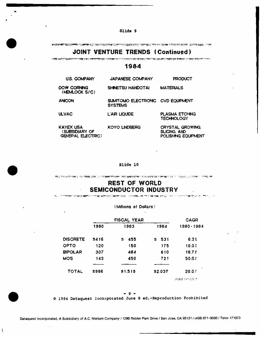
Slide 9
JOINT VENTURE TRENDS (Continued)
1984
U.S. COMPANY
DOW CORNING (HEMLOCK S/C)
ANICON
ULVAC
KAYEX USA (SUBSIDIARY OF
GENERAL ELECTRIC)
JAPANESE COMPANY PRODUCT
SHINETSU HANDOTAI MATERIALS
SUMITOMO ELECTRONIC CVD EQUIPMENT SYSTEMS
LAIR LIQUDE
KOYO LINDBERG
PLASMA ETCHING TECHNOLOGY
CRYSTAL GROWING. SLICING. AND POLISHING EQUPMENT
Sl ide 10
.;;«^''<*<r^ :• :-v;:'i-^w!^-r;>^;;fle-::; .;-;'r;' :}fi5«l' .«"V^^ i x -*; ;i jflji«;^-»;w;:< -; i^'";-^:.r;''!-}f-!';i'ii*;''W; T V ' "'^:>i^V, ',--'"^^",'-V-^'' '-"^rj ^
REST OF WORLD SEMICONDUCTOR INDUSTRY
(Millions of Dollars)
DISCRETE
OPTO
BIPOLAR
MOS
TOTAL
1880
S416
120
307
143
S986
FISCAL YEAR
1983
$ 455
150
464
450
$1,519
1984
S 531
175
610
721
$2,037
CAGR
1980-1984
6.3%
lo.oi; 18.73?
50.0i?
20.07
- 9 -O 1984 Dataquest Incorporated June 8 ed.-Reproduction Prohibited
Dataquest Incorporated, A Subsidiary of A.C. Nielsen Company /1290 Ridder Park Drive / San Jose, CA 95131 / (408) 971-9000 / Telex 171973
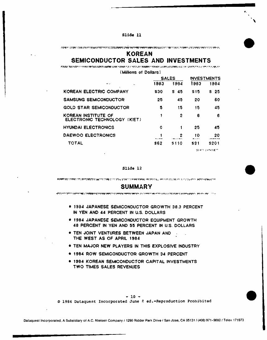
Slide 11
• . j ^ : ij«fj:i*\->^-:i?'5fK4:i .••-:'^i«-'^"i ; ; ' ^ ^
KOREAN SEMICONDUCTOR SALES AND INVESTMENTS
(ispsaw^^wwfiiSjs^wi-^^ass^i^^^i^^s^rifa^
(Millions of Dollars]
KOREAN ELECTRIC COMPANY
SAMSUNG SEMICONDUCTOR
GOLD STAR SEMICONDUCTOR
KOREAN INSTITUTE OF ELECTRONIC TECHNOLOGY (KIET)
HYUNDAI ELECTRONICS
DAEWOO ELECTRONICS
TOTAL
SALES 1983
$30
25
5
1
0
1
$62
1984
$ 45
45
15
2
1
2
$110
INVEST 1983
$15
20
15
6
25
10
$91
'MENTS 1984
$ 25
60
45
6
45
20
$201 fiiii:-.- [,_T,^r,.if-
Sl ide 12
SUMMARY
• 1984 JAPANESE SEMICONDUCTOR GROWTH 38.3 PERCENT IN YEN AND 44 PERCENT IN U.S. DOLLARS
• 1984 JAPANESE SEMICONDUCTOR EQUIPMENT GROWTH 48 PERCENT IN YEN AND 55 PERCENT IN U.S. DOLLARS
• TEN JOINT VENTURES BETWEEN JAPAN AND • THE WEST AS OF APRIL 1984
• TEN MAJOR NEW PLAYERS IN THIS EXPLOSIVE INDUSTRY
• 1984 ROW SEMICONDUCTOR GROWTH 34 PERCENT
• 1984 KOREAN SEMICONDUCTOR CAPITAL INVESTMENTS TWO TIMES SALES REVENUES
- 10 -1984 Dataque.'st Incorporated June P. ed.-Reproduction Prohibited
Dataquest Incorporated, A Subsidiary of A.G. Nielsen Company / 1290 Ridder Park Drive / San Jose, CA 95131 / (408) 971-9000 / Telex 171973
Dataquest RESEARCH NEWSLETTER
Code; EIEJ Newsletters
JAPAN'S SECOND VENTURE CAPITAL BOOM
SUMMARY
Since 1982, Japan has experienced a second boom in venture capital activity, popularly known as "benchaa boomu" (venture boom) in the Japanese press. According to the Ministry of International Trade and Industry (MITI), venture capital investments in high-technology venture businesses (start-ups) leaped tenfold, from ¥2.2 billion ($10.0 million) in 1981 to ¥22.9 billion ($97.4 million) in 1983. (See Figure 1.)
This investment growth is being driven by the entry of 16 new venture capital companies and by the influx of American venture capitalists. Although there are still many obstacles to a vibrant venture capital market in Japan, DATAQUEST believes that this recent upsurge in investment activity shows greater potential than the first boom that began in the early 1970s. The creation of an American-style over-the-counter (OTC) stock market in November 1983, the increasing liberalization of the Japanese capital market, and the proliferation of Japanese venture businesses in software and other high-technology fields will create numerous opportunities for foreign investors.
© 1984 Dataquest Incorporated May 29 ed.-Reproduction Prohibited
The con len i of ihis repon represents our mterpreial ion and analysis o1 intormal ion generally available lo Ifie public or 'eieased b
provided to us m conf idence by our cl ienis Individual conipames reported on and analyzed bv DATAQUEST may be c l ien lsof t h i s ,
wi th ihe solicitat ion of an offer to buy securit ies This firm and its parent and/or iheir officers stochnoiders or mefTiOers of their i
Donsible individuals in tfie subject companies but is not guaranteed as to accuracy or completeness It does not contain materi
1 Olfier DATAQUEST services Tfiis information is not furnished in connect ion with a sale or offer to sell securit ies or in connectn
es rnay Irom time lo time nave a long or shori posit ion in the securit ies mentioned and may sell or buy such securit ies
Dataquest Incorporated, A Subsidiary of A.C. Nielsen Company / 1290 Bidder Park Drive / San Jose, CA 95131 / (408) 971-9000 / Telex 171973
Figure 1
VENTtntE CAPITAL INVESTMENTS IN JAPANESE HIGH-TECHNOLOGY COMPANIES
c v
n c .2 (D
2 2 -
20 -
1 8 -
1 6 -
14 -
1 2 -
10 -
8 -
6 -
4 -
2 -I
O -
/
• /
1— - I — 1 1 r - I — 1977 1978 1979 1980 1981 1982 1983
Source: DATAQUEST
THE FIRST VENTDRE BOOM
In the early 1970s, Japan experienced its first "venture boom" as eight venture capital companies were established. As shown in Table 1, these firms were owned primarily by major Japanese banks, securities companies, and life insurance cranpanies. Unlike American venture capital firms, they were staffed exclusively by traditional financial analysts, and lacked in-house technology experts. Moreover, these firms did not offer management or marketing consulting services. Consequently, few of the early Japanese venture capital companies invested in high-risk, leading-edge technologies, but put their yen into more mature retailing, wholesaling, and consumer manufacturing companies that were preparing to go public.
- 2 -
Table 1
THE FIRST BOCM IN JAPANESE VENTURE CAPITAL COMPANIES
Company
Nippon Enterprise Development Corp. (NED)
Kyoto Enterprise Development Corp.
Japan Associated Finance Co. (JAFCO)
Universal Finance Co.
Central Capital Co.
Techno-Venture Co.
Tokyo Venture Capital Co.
Diamond Capital Co.
Date Established
NOV. 1972
1972 (closed 1979)
April 1973
Dec. 1973
Jan. 1974
Feb. 1974
April 1974
Aug. 1974
Major Shareholders
Long-Term Credit Bank of Japan Daiwa Securities
Omron Tateishi Electronics Co. Bank of Kyoto
Nomura Securities Nippon Life Insurance
Yamaichi Securities Dai-Ichi Life Insurance
Nikko Securities, Tokai Bank
Japan Industrial Bank Hitachi Works
Dai-Ichi Kangyo Bank Kangyo Kakumaru Securities
Mitsubishi Bank Tokyo Fire & Marine Insurance
Source: DATAQUEST
This conservative approach was reinforced after a series of wild investment schemes rocked the country in the aftermath of the 1973 oil shock. To protect investors, the Ministry of Finance imposed strict rules for new company listings and trading in 1976. Companies wanting to be listed had to meet minimum capital, earnings, and dividend requirements for a period of several years prior to their request. As a result, daily trading volumes were miniscule, and the OTC market rapidly became known as a graveyard for financially troubled companies that had slipped off the Tokyo and Osaka stock exchanges.
- 3 -
THE SECOND VENTURE BOCM
Since early 1982, Japan has experienced a second venture boom with the emergence of 16 new venture capital companies, as shown in Table 2. Dubbed the "era of small ventures," this renewed activity is being fueled by a variety of factors:
Rapid growth in high-tech industries, such as semiconductors, computers, software, ceramics, and biotechnology
Broader, more diversified consumer demand for custom products incorporating new technologies
Investment shift away from declining heavy industries
More investors attracted to venture businesses to secure higher returns and new business partners
Revision of the Foreign Exchange and Trade Control Act (1979) that liberalized foreign capital transactions
Entry of U.S. venture capital companies and more activity by U.S. banks and securities companies
Appearance of more adventurous entrepreneurs, especially among mid-career professionals and college graduates who were educated 4broad and are employed with foreign companies
These new venture capital companies are markedly different from the first wave of companies. Generally, they are backed by Japanese securities firms, foreign investors, and government banks such as the Long-Term Credit Bank of Japan and the Industrial Bank of Japan. Moreover, these companies are working through the securities and over-the-counter markets, and are willing to provide early-stage equity investments in high-tech ventures, such as software and computer start-ups. Because of their independence from large Japanese banks, these companies are playing a more aggressive role. Probably the most significant change is the entry of foreign investors, especially American venture capitalists, who provide sophisticated technology evaluation and management consulting services.
- 4 -
Table 2
THE SECOND BOCM IN JAPANESE VENTURE CAPITAL COMPANIES
Company
Jamil Group S.I.
Japan Investunent Finance Co.
Sanyo Finance Co.
Pacific Technology Ventures Inc.
Yamaichi Uni-Ven. Co.
New Japan Finance Co,
Wako Finance Co.
Marusan Finance Co.
Okasan Finance Co.
Maruman Finance
Date Established
Jan. 1982
Aug. 1982
Aug. 1982
Sept. 1982
NOV. 1982
Dec. 1982
Dec. 1982
March 1983
April 1983
Kansai Venture Capital May 1983
June 1983
Pariba-Ven Japan June 1983
Fidelity Japan Aug. 1983
CFB Venture Capital Corp. Sept. 1983
Orient Capital Co. Oct. 1983
Micro Technology Corp. Nov. 1983
Major Shareholders
Jamil Group (Saudi Arabia)
Daiwa Securities Long-Term Credit Bank of Japan
Sanyo Securities Group
Pacific Ventures Technology Management Co. (San Francisco)
Yamaichi Securities
New Japan Securities Industrial Bank of Japan
Wako Securities Industrial Bank of Japan
Marusan Securities
Okasan Securities Industrial Bank of Japan
Osaka-ya Securities Daiwa Bank
Maruman Securities Tokai Bank
Banque de Paris et des Pays-Bas
Fidelity Venture Associates (U.S.)
California First Bank (Bank of Tokyo)
Orient Leasing Co. (Tokyo) Baring Brothers (London) Hambrecht & Quist (San Francisco)
Pacific Capital Fund (California) Global Commercial (Tokyo) S.G. Inc. (Tokyo)
Sou rce: DATAQUES T
- 5 -
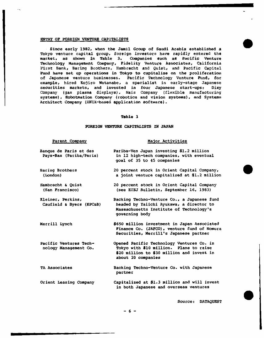
ENTRY OF FOREIGN VENTURE CAPITALISTS
Since early 1982, when the Jamil Group of Saudi Arabia established a Tokyo ventuire capital group, foreign investors have rapidly entered the market, as shown In Table 3. Companies such as Pacific Venture Technology Management Company, Fidelity Venture Associates, California First Bank, Baring Brothers, Hambrecht and Quist, and Pacific Capital Fund have set up operations in Tokyo to capitalize on the proliferation of Japanese venture businesses. Pacific Technology Venture Fund, for example, hired Kojiro Watanabe, a specialist in early-stage Japanese securities markets, and invested in four Japanese start-ups; Dixy Company (gas plasma displays) , Nais Company (flexible manufacturing systems) , Robotmation Company (robotics and vision systems), and Systems Architect Company (UNIX-based application software).
Table 3
FOREIGN VENTURE CAPITALISTS IN JAPAN
Parent Company Major Activities
Bangue de Paris et des Pays-Bas (Pariba/Paris)
Pariba-Ven Japan investing $1.2 million in 12 high-tech companies, with eventual goal of 35 to 45 companies
Baring Brothers (London)
20 percent stock in Orient Capital Company, a joint venture capitalized at $1.2 million
Hambrecht & Quist (San Francisco)
20 percent stock in Orient Capital Company (see EIEJ Bulletin, September 16, 1983)
Kleiner, Perkins, Caufield & Byers (KPC&B)
Backing Techno-Venture Co., a Japanese fund headed by Yaiichi Ayukawa, a director to Massachusetts Institute of Technology's governing body
Merrill Lynch $650 million investment in Japan Associated Finance Co. (JAFCO), venture fund of Nomura Securities, Merrill's Japanese partner
Pacific Ventures Technology Management Co.
Opened Pacific Technology Ventures Co. in Tokyo with $10 million. Plans to raise $20 million to $30 million and invest in about 20 companies
TA Associates Backing Techno-Venture Co. partner
with Japanese
Orient Leasing Company Capitalized at $1.3 million and will invest in both Japanese and overseas ventures
Source: DATAQUEST
- 6 -
Foreign companies are also entering into joint ventures with Japanese financiers to establish an "insider" presence in Tokyo. Baring Brothers and Hambrecht & Quist, for example, have teamed up with Orient Leasing Company, while Pacific Capital Fund has joined with S.G. Inc. and Global Commercial, both of Tokyo. The revision of the Foreign Exchange and Trade Control Law in 1979 has facilitated these activities by permitting a freer flow of foreign capital and reducing MITI's control over joint ventures.
Japanese Venture Capitalists Waking Op
One spin-off benefit caused by the foreign investors is the reawakening of Japan's lethargic venture capital market. American investors have introduced strong competition and new investment techniques that are changing the nature of the Japanese venture capital market. Existing companies such as the Japan Associated Finance Company (JAFCO), for example, are investing more money in high-technology ventures and offering management consulting services. Recently, JAFCO's president, Teiji Imahara, launched JAFCO II, a venture capital fund that now has more than V12.5 billion ($53 million) in the form of partnerships. JAFCO also opened a Hong Kong subsidiary to expand into Southeast Asia. In addition, three Japanese securities houses—Daiwa Securities, Nomura Securities, and Yamaichi Securities—introduced computerized investment services in December 1983 to open the Japanese securities markets to more foreign investors. DATAQUEST believes that these activities are signs that the Japanese venture capital market is finally waking up.
A NEW OVER-THE-COONTER MARKET
A major development is the creation of an American-style over-the-counter stock market by the Japanese government in November 1983. The change came after much lobbying by MITI and the Japan Securities Dealers Association, and on the recommendation of the Securities Exchange Council. The new rules, which are stricter than NASDAQ's, require a net worth of about $850,000, and pretax profits of more than 4 cents a share for listing. About 12,000 companies would qualify under these liberalized rules, although insiders only expect several hundred to be traded within the next few years. DATAQUEST believes that these new rules will open numerous opportunities for foreign investors, especially in the high-technology fields being pushed by MITI such as biotechnology, fine ceramics, software, electronic machinery (mechatronics), and computers.
- 7 -
MITI'S NEW ROLE
MITI has actively promoted the creation of a venture capital market and venture businesses—the engines for Japan's future economic growth. In 1975, MITI set up a Venture Enterprise Corporation (VEC) to guarantee up to 80 percent of a venture's bank borrowing for product development. But most entrepreneurs shied away, to avoid the burdensome paperwork and the MITI influence. Since its founding, VEC has funded only about $30 million.
During this boom, MITI is downplaying its intervention and emphasizing market incentives, as shown in Figure 2. In February 1984, MITI and the Small Business Agency announced a venture business subsidy program consisting of four financing systems:
• A new credit program at the Small Business Finance Bank that will issue loans up to ¥330 million ($1.5 million) at 8.1 percent for 15 years to high-tech companies
• An R&D subsidy program for new ceramics, mechatronics, and other high-tech product development
• Subsidies to 18 small and medium-size business cooperatives engaged in new ceramic research projects
• Subsidies to local industrial testing stations for purchasing mainframe computers and other expensive equipment
MITI is also formulating a "Venture Business Promotion Law" that is scheduled to be introduced in fiscal 1985. This legislation will probably propose new financial measures and technical guidance for high-tech venture businesses, based on the results for the four programs mentioned above.
DATAQUEST believes, however, that there will be heated discussion between MITI and the Ministry of Finance (MOF) over this legislation because of their conflicting interests. MITI wants to gain control over the emerging OTC market to help nurture high-tech venture business. Early-stage program financing would give it major involvement in these sunrise industries. However, MOF is afraid of losing its traditional control over the securities market. In particular, the major Japanese banks, already plagued with too much competition, worry about losing customers to the new venture capital companies. They insist on developing long-term mutual relationships, not just short-term financing arrangements typical of venture capital firms. We expect to see MITI make compromises over its proposed involvement .in the OTC market in order to secure passage in the Diet.
- 8 -
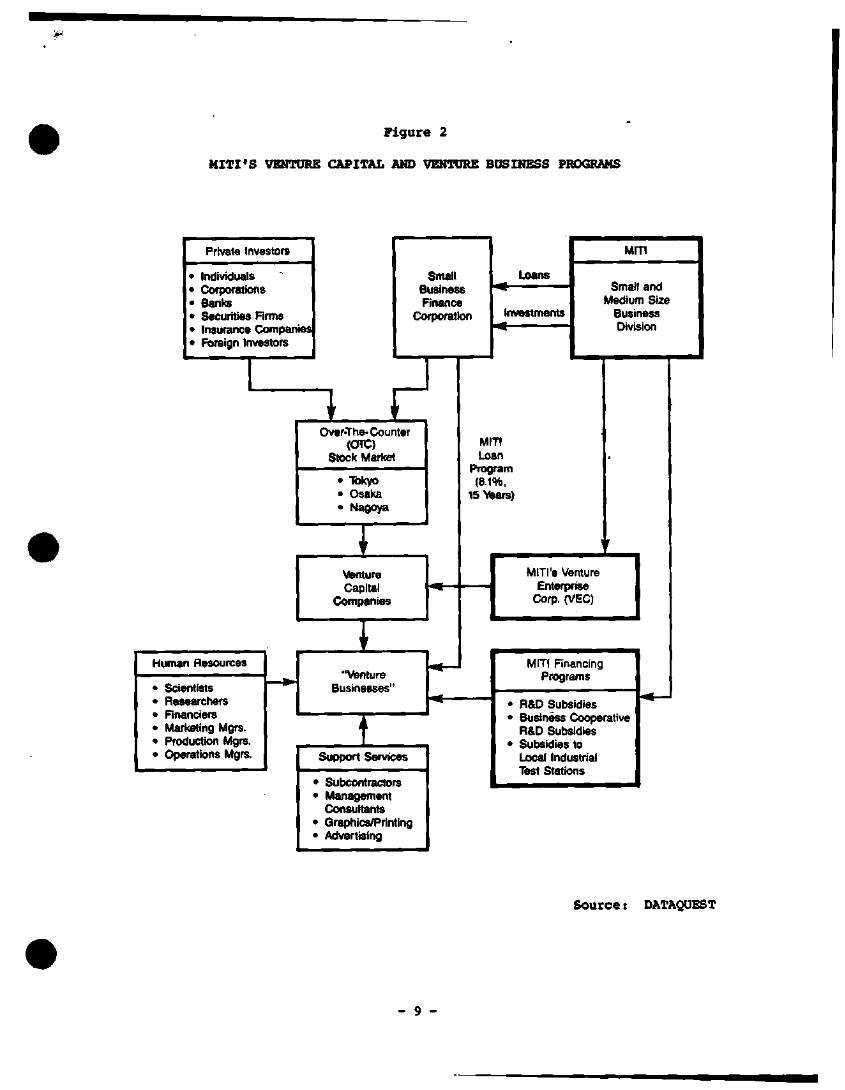
Figure 2
MITI'S VENTURE CAPITAL AND VENTURE BUSINESS PROGRAMS
Private Investors
• Individuals • Corporations • Banks • Securities Firms • Insurance Companies • Foreign Investors
Human Resources
• Scientists • Researchers • Financiers • Marketing Mgrs. • Production Mgrs. • Operations Mgrs.
1
B F
Co
_
\ Over-The- Cou nter
(OTC) Stock Market
• Tokyo • Osaka " Nagoya
1 Venture Capital
Companies
1 "Wsnture
Businesses"
1 I
Support Services
• Subeorrtractnrs
• Manage ConsuIt
• Graphic • Advertis
»ment ants is/Printing iing
Small usiness 'inance rporation
Loans
Investments
MITI
Small and Medium Size
Business Division
MITI Loan
Program (8.1%,
15 V^ars)
^
•
' f
MITI'S Venture Enterprise
Corp. (VEC)
MITI Financing Programs
• R&D Subsidies • Business Cooperative
R&D Subsidies • Subsidies to
Local Industrial Test Stations
Source: DATAQUEST
- 9 -
MAJOR OBSTACLES
Despite the emergence of new capital companies and an OTC market, there are still many obstacles blocking the establishment of an active venture capital market and venture businesses in Japan. These include:
• Shortage of new venture businesses due to a lack of entrepreneurial spirit (although this is changing)
• Japan's lifetime employment system which discourages spin-offs and job-hopping
• Strong reluctance to give up part of a company to outside investors and venture capitalists (family traditions)
• Federal Trade Commission rules preventing venture capital firms from placing their employees on venture business staffs and prohibiting venture capitalists from acquiring more than 49 percent ownership
• The low-risk, low-return strategy of most Japanese venture capital companies
• Close ties between venture capital companies and large banks (keiretsu)
• Aversion to head-hunting services and raiding to secure qualified managers
• Lack of experience in evaluating new technologies and entrepreneurs and in providing management consulting
Although it will take time before it becomes socially acceptable in Japan to leave one's employer and start one's own company, we see signs of change among young college graduates, working women, mid-career professionals impatient with their slow progress in large corporations, and retirees looking for a second career. According to a recent survey by the Prime Minister's Office, about five million people, or 8.6 percent of the Japanese work force would like to change jobs if given the opportunity. This figure is more than double the 2.5 million people (4.9 percent of the work force) who expressed interest in job-hopping in 1971. Moreover, DATAQUEST believes the influence of Silicon Valley should not be underestimated as Japan shifts to high technology. For millions of Japanese workers faced with the prospect of "lifetime imprisonment" in companies they dislike, the U.S. attitude toward job-hopping, and our more flexible hiring practices seem like heaven.
Sheridan Tatsuno Nagayoshi Nakano
- 10 -
Dataquest RESEARCH NEWSLETTER
EIEJ Code: Newsletters
TRADITION BREAK FOR TEXAS INSTRUMENTS
INTRODUCTION
In a sharp break with the past, Texas Instruments announced that it will join the World Trade Statistics Program, originally sponsored by the Semiconductor Industry Association. TI has also decided to participate in the Semiconductor Research Cooperative, which was founded to conduct basic research through a pooling of resources.
DATAQUEST believes that TI's willingness to provide confidential sales figures to Price Waterhouse for incorporation with statistics of other U.S, European, and, recently, Japanese manufacturers is part of a strategy to move aggressively in this currently supply-limited market. We see the Dallas-based manufacturer aggressively expanding its gate array, standard cell, and CMOS business in order to keep pace with both the Japanese and with the current U.S. market leaders. Motorola and National. It is our opinion that the CMOS semiconductor market has the highest growth potential of the industry's emerging new product opportunities.
AN AGGRESSIVE NEW STRATEGY
As shown in Table 1, TI is pursuing an aggressive strategy to capture share of the microcontroller and rapidly growing application-specific IC (ASIC) markets. In 1983, TI signed second-sourcing agreements with Seeq and General Instrument for its successful TMS7000 8-bit MCU. In the gate array field, TI has joined with Fujitsu, Japan's strongest semicustom maker, to second-source Fujitsu's bipolar and CMOS arrays. Harris will second-source TI's CMOS gate arrays, which are being designed according to military specifications under the VHSIC program.
© 1984 Dataquest Incorporated May 30 ed.-Reproduction Prohibited
The content o( ihis repori represents our interpreiat ion and analysis o( Inlormation generally available lo ihe puDhc or released Dy esponsib le individuals m ine subiecl companies but is not guaranteed as to accuracy or completeness It does nol contatn nriaierIal
provided to us m conddence by our cl ients IndIvIdual companies reported on and analyzed by 0* rAQiJEST mav be clients o ' ihis and.or other DATAOLJEST services This Intormaiion is not furnished m connection with a sale or ol tef to sell securities or in connection
with the sol ici tat ion o( an oHer to buy secufi t ies This firm and us parent and'or their otdcers stockholders or memoers oi meir iani,i,es ma^ trom i,me to i ime have a long or short posit ion m the securit ies meni ioned and may sell or buy sucti securit ies
Dataquest Incorporated, A Subsidiary of A.C. Nielsen Company /1290 Bidder Park Drive / San Jose, CA 95131 / (408) 971-9000 / Telex 171973
Although TI's sales of CMOS devices have grown at a compound annual growth rate (CAGR) of 35.7 percent since 1980, Tl has lost revenues to companies offering CMOS gate arrays, such as LSI Logic. To strengthen its position in the semicustom market, Tl has moved aggressively in several directions:
• Developing a 2.0-2.5 urn CMOS process in Houston
• Merging its gate array product center and design automation into the Custom Components Division in Dallas and introducing a line of CMOS standard cell logic for integrating 54/74 logic functions
• Adapting its in-house Transportable Integrated Design Automation Language (TIDAL) to run on Apollo 32-bit type workstations
• Licensing its CAD system in exchange for second-sourcing Fujitsu's bipolar and CMOS gate arrays
• Adding 4 design centers in Europe (Bedford, England; Paris, Prance; Frankfurt, Germany; and Milan, Italy) to its 12 centers in the United States
• Offering two levels of design for its standard cell customers
CONCLUSION
We believe that TI's move to join the World Trade Statistics Program and form partnerships in new technologies to fill voids in its product line will prove helpful in TI's quest to regain its leadership position.
Sheridan Tatsuno Gene Norrett
- 2 -
Table 1
TI*S RECENT LICENSING AGREEMENTS AND JOINT VENTURES
Date
Feb. 83
Feb. 83
March 83
Partner
Seeq
Harris
General Instrument
Agreement
Application of Seeq's EEPROM technology to TI's TMS7000 8-bit MCU
Harris to second-source TI's 1000-and 2000-gate mil-spec CMOS gate arrays (VHSIC program)
GI to second-source TI's 8-bit TMS7000 MCU
July 83 VLSI Technology, Inc. (VTI)
VTI to second-source TI's TMS4500A 64K DRAM controller and develop new CMOS circuit for TI's 256K DRAM
July 83
Nov. 83
Jan. 84
May 84
Western Digital
General Instrument
Fujitsu
National
Mutual second-sourcing of Western Digital's communications controllers and TI's universal uP peripherals
GI to second-source TI's TMS320, an NMOS digital signal processor, and develop a CMOS version
TI to provide its CAD design for Fujitsu's bipolar and CMOS gate arrays
Second-source 32-bit MPU
Source: DATAQUEST
- 3 -
Dataquest RESEARCH BULLETIK
EIEJ Code: Newsletters
A SECOND NTT TAKES SHAPE
Five Japanese companies are making a bold move into the telecommunications business in anticipation of the divestiture of Nippon Telegraph and Telephone (NTT) next year. Kyocera, Sony, Ushio Electric, Secom, and Mitsubishi Corporation have announced that they will establish the "Second NTT Planning Company" on May 31. Headed by Shingo Moriyaraa, Vice President of Kyocera, the new company will be capitalized at VI.6 billion ($7.0 million) and will also involve twenty other companies, including telecommunication manufacturers, banks, securities companies, and trading houses. The five founding companies will hold 50 percent ownership; stock participation outside the initial 25 companies will be available in mid-July. As shown in Table 1, the five companies are well-positioned technically and financially.
The Second NTT Planning Company plans to build a $130 million fiber-optic link along expressways between Tokyo and Osaka, to be operational in 1988. This system will offer phone and data services, and parlay the technical expertise of the five founding companies in large-scale construction projects and home electronics. It will compete directly with NTT's Information Network System (INS) which is scheduled for nationwide operation by 1987 (see our discussion of NTT's INS development plans in the DATAQUEST JSIA notebook. Section 1.2-23). However, Kyocera believes that the new service will be immediately profitable since its rates will be based on the initial link in the heavily used Tokyo-Nagoya-Osaka corridor, not on a nationwide network as with NTT's INS program. An independent survey estimates that fees for the second NTT service would be only 20 percent of NTT's current rates.
Although Yoshinori lida, an executive with NTT's New York office, said NTT welcomes the competition because it would justify the deregulation process, DATAQUEST believes that approval of the second NTT system by the Ministry of Posts and Telecommunications (MPT) will not be easy. Traditionally, MPT has been very protective of NTT, as shown in the recent value-added network (VAN) controversy with the United States. The construction of a second NTT network would cause substantial losses in revenue to NTT's $120 billion INS System—something that MPT or NTT is unlikely to welcome. Moreover, approval of the new system is likely to
© 1984 Dataquest Incorporated May 30 ed.-Reproduction Prohibited
tn p :]jin1 rtn L uH <l»i*f#tifliL rtHJHrtJi n1 abI+ ir.f^TtHt'l M(Ki ^nCflnft l^ i l* ' itH^^lt^l iti^ IIJ*'JMi # ^iitdHjiF.llI fftfl SUtih: W 'V\^9\^t't I BiponJ^I^I* ' npni-tlHjtt* ifi TTlf I v t H " ! ir«^-H*v« 1!*1' k nV^mniJiri ic*u 111 lii^tiL^L'K^ U ^ l1iV0 Kii ltnflj;i Jl BiM .rIiI
•111 •L-Itfj] Vurtf 'JI'* ijvu'.vtp.- ' h^niT ^liYiitiLt'I'-nnn'T.T^^^r^rrhhtf —• jr4dJuJIfftl t i bAl4lkJllSt. ^IV bif tl 'trnt^ dMt^ll 44>Jrnr dlrnr ^14f AUUt ST %»nc:*k Triri iftltV11kjL«S'4-hA^ 1 U'ILJri'ipfl 1 rr£[} i<fl<HifiHt'-fiim 1 U|> lrt JlI^M.^^in| 1 lllH;i>niH<
—ith ttid Ml ^ 1 tjil'0"0'r+^n»T» tn•"<•» ^ficuiin** Tn-iJuiti^y i l*r*fF" '* ' "^ur •ihUbi nHiLr-i iiniL^miliiiiIii rnTtii4fiSii'iv,iFitifiP inrTiIi4P> wi4i ^^llml^frt ifilivrr* fl^^^^ » I*i^3^ ITOH'UL->IH'^- m IIIH t^ l j 'Hiui i n-ili^ Ini^T n ; -tr ^r u' ri •* nr" f*-
-,iM|UHhLp^n„iii
n'MI Qonn»rr-int
. f l i r r
Dataquesl Incorporated, A Subsidiary of A.C. Nielsen Corripany / 1290 Rldder Park Drive ' San Jose, CA 95131 / (-108) 971-3000 / Teiex 171973
be fiercely contested by the major Japanese telecommunications companies who would oppose the second NTT's effort to take the "cream" of the lucrative Tokyo-Nagoya-Osaka market. They would be effectively locked out of the second NTT since the five founding companies hold majority ownership. Added to this is the fierce competition posed by the entry of the Japan National Railways, Japan Highway Corporation, AT&T, IBM, ITT, Corning Glass Works, and other foreign companies into the Japanese fiber-optics market.
Thus, we believe that the second NTT is not yet an established fact but just the beginning of a long-running controversy, as Japan attempts to deregulate its telecommunications industry. However, NTT divestiture and the formation of a second NTT will create many marketing opportunities for foreign semiconductoc companies selling optoelectronic ICs, optocouplers, semiconductor lasers, and other optoelectronic devices.
Table 1
FOUNDING COMPANIES OF THE SECOND NTT
Sheridan Tatsuno
Company
Kyocera
Mitsubishi Corporation
Major Products
Ceramic IC packaging (70% of world market), OA equipment
Largest trading company in Japan; strong in heavy electrical power equipment
FV1983 Revenues ($ Millions)
$ 723.4
$31,489.4
Secom (Nihon Reibi Hosho)
Sony
Ushio Electric
Electronic security systems (60% of Japanese market
Consumer electronics, semiconductors, floppy disks, word processors
Halogen and xenon lamps for semiconductors, OA equipment, automobiles, and optical equipment
$ 127.7
$ 3,277.0
$ 33.6
Source: DATAQUEST
- 2 -
CMf.'J Dataquest RESEARCH NEWSLETTER
EIEJ Code: Newsletters
CAN MCC CATCH UP WITH JAPAN?
Microelectronics and Computer Technology Corporation (MCC), a consortium of 15 major American electronics companies established in 1982 to beat Japan in creating a fifth-generation computer, announced six research directors on April 10, 1984. A research director for the Software Development Program will be announced in mid-May. As shown in Table 1, MCC has selected a team of highly qualified individuals to run its research programs that are formally under way. MCC currently has 110 employees working at its temporary facility, with plans to have the participating companies lend 140 more researchers by 1985. A permanent facility will be built at the University of Texas beginning this year and is scheduled to open in the fall of 1985.
MCC was formed in 1982 by 10 American microelectronics and computer companies. Since then, 5 additional companies have become full participants or shareholders, bringing the total to 15, as shown in Table 2. Each shareholder company must commit funds and staff to support MCC's research program for at least three years. The entry fee is $200,000. Shareholder companies will have exclusive access to research findings for three years after the completion of the project. The research or patents may be licensed and revenues then become the property of MCC. MCC has a funding goal of $324 million, of which $30 million was committed by the founding 10 companies in 1983. In addition, the University of Texas announced on April 10 a $32 million funding package for computer science programs, consisting of $8 million from a private donor. University of Texas oil lands revenues, and private matching funds from 5 Texas foundations. Although not directly benefitting MCC, this funding will provide a local source of trained researchers in the future.
MCC has scheduled four long-range advanced technology programs, as shown in Table 3.
DATAQUEST believes MCC has the potential to achieve major breakthroughs in semiconductor and computer technology. However, the project is several years behind Japan's Fifth Generation Computer Project (1979-1991) and four years behind its Supercomputer (1981-1989) and New Semiconductor Functions Project (1981-1990). We have already observed the beginning of a "patent deluge" from these projects. The New Functions
® 1984 Dataquest Incorporated April 30 ed.-Reproduction Prohibited
The conlent of ihIs feport represents our Inlerpretaiion and arialysis of intormal Ion generally availaDle lo t^e public or released
Droviidei] lo us In conl idence by our clients IndivIIjual companies reported on and analyzed by DATAQUEST may be clients ol this
with ihe sol Ici lat ion ol an otter to buy securit ies Tfiis lIrm and Its parent and/or ilieIr off icers stockl iolders or members oi ineir
y respc
aid'Or
a-T,.iies
nsible indIvIduals I
tber DATAQUEST s
may l,om hme lo i
Ihe subject companies but Is n
ervices ThIs informatIon is not fu
n e l - , . . e , l „ „ g o , s « o , i p o s , . o n
, guarameed as
rnIshed In conn
n t . e sccu r I „e .
loaccuracy or completeness
eel ion with a sale or offer to sel
meni ionec ana may sell or buy
t does not coniaIr
securit ies or In cc
Such seCutit.BS
materIai
nnecHon
Dataquest Incorporated, A Subsidiary of A.C. Nielsen Company /1290 Bidder Park Drive / San Jose, CA 95131 / (408) 971-9000 / Telex 171973
Project, for example, recently submitted 147 patent applications for 3-dimensional ICs. The real question for MCC is not whether it can produce innovative research; we believe it will. But rather, can it catch up with Japan?
For more information on MCC, contact:
Dr. William D. Stotesbery Director, Government and Public Affairs Microelectronics and Computer Technology Corporation 9430 Research Blvd. Echelon Building #1, Suite 200 Austin, Texas 78759-6509 Phone: (512) 343-0860
Sheridan Tatsuno
- 2 -
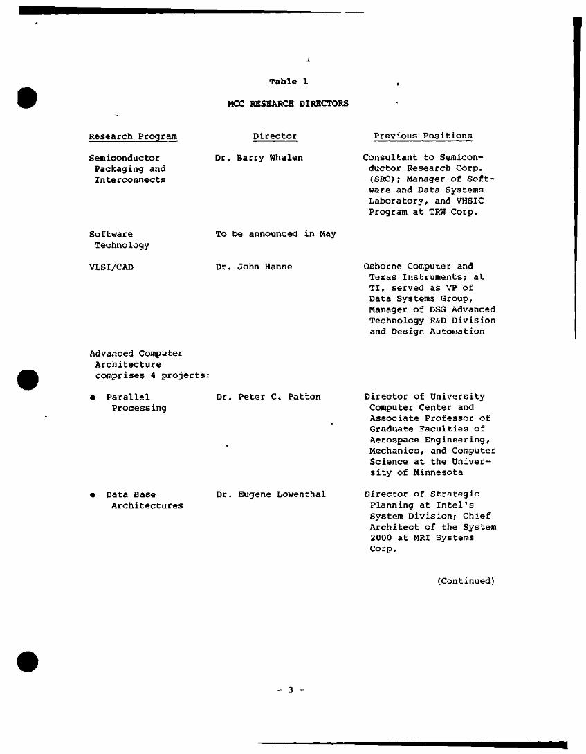
Table 1
MCC RESEARCH DIRECTORS
Research Program
Semiconductor Packaging and Interconnects
Software Technology
VLSI/CAD
Director
Dr. Barry Whalen
To be announced in May
Dr. John Hanne
Advanced Computer Architecture comprises 4 projects:
• Parallel Processing
Dr. Peter C. Patton
Data Base Architectures
Dr. Eugene Lowenthal
Previous Positions
Consultant to Semiconductor Research Corp. (SRC); Manager of Software and Data Systems Laboratory, and VHSIC Program at TRW Corp.
Osborne Computer and Texas Instruments; at TI, served as VP of Data Systems Group, Manager of DSG Advanced Technology R&D Division and Design Automation
Director of University Computer Center and Associate Professor of Graduate Faculties of Aerospace Engineering, Mechanics, and Computer Science at the University of Minnesota
Director of Strategic Planning at Intel's System Division; Chief Architect of the System 2000 at MRI Systems Corp.
(Continued)
3 -
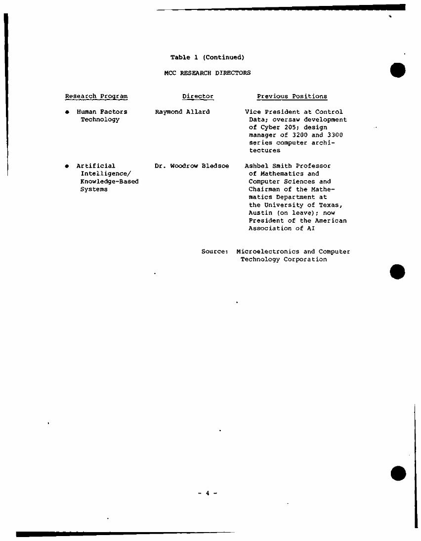
Table 1 (Continued)
MCC RESEARCH DIRECTORS
Research Program
• Human Factors Technology
Artificial Intelligence/ Knowledge-Based Systems
Director
Raymond AHard
Dr. Woodrow Bledsoe
Previous Positions
Vice President at Control Data; oversaw development of Cyber 205; design manager of 3200 and 3300 series computer architectures
Ashbel Smith Professor of Mathematics and Computer Sciences and Chairman of the Mathematics Department at the University of Texas, Austin (on leave); now President of the American Association of AI
Source: Microelectronics and Computer Technology Corporation
4 -
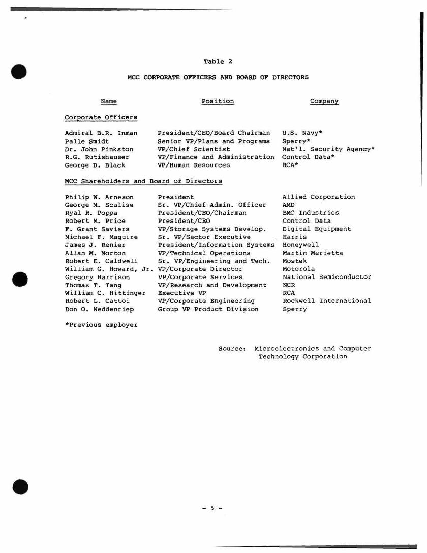
Table 2
MCC CORPORATE OFFICERS AND BOARD OF DIRECTORS
Name
Corporate Officers
Admiral B.R. Inman Palle Smidt Dr. John Pinkston R.G. Rutishauser George D. Black
Position
President/CEO/Board Chairman Senior VP/Plans and Programs VP/Chief Scientist VP/Finance and Administration VP/Human Resources
MCC Shareholders and Board of Directors
Philip W. Arneson George M. Scalise Ryal R. Poppa Robert M. Price F. Grant Saviers Michael F. Maguire James J. Renier Allan M. Norton Robert E. Caldwell William G. Howard, Jr, Gregory Harrison Thomas T. Tang William C. Hittinger Robert L. Cattoi Don O. Neddenriep
•Previous employer
President Sr. VP/Chief Admin. Officer President/CEO/Chairman President/CEO VP/Storage Systems Develop. Sr. VP/Sector Executive President/Information Systems VP/Technical Operations Sr. VP/Engineering and Tech. VP/Corporate Director VP/Corporate Services VP/Research and Development Executive VP VP/Corporate Engineering Group VP Product Division
Company
U.S. Navy* Sperry* Nat'l. Security Agency* Control Data* RCA*
Allied Corporation AMD BMC Industries Control Data Digital Equipment Harris Honeywell Martin Marietta Mostek Motorola National Semiconductor NCR RCA Rockwell I n t e r n a t i o n a l Sperry
Source: Microelectronics and Computer Technology Corporation
- 5 -
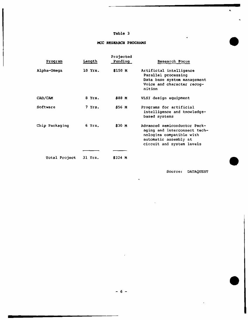
Table 3
MCC RESEARCH PROGRAMS
Program
Alpha-Omega
CAD/CAM
Software
Chip Packaging
Length
10 Yrs.
8 Yrs,
7 Yrs.
6 Yrs.
Projected Funding
$150 M
$88 M
$56 M
$30 M
Total Project 31 Yrs. $324 M
Research Focus
Artificial intelligence Parallel processing Data base system management Voice and character recognition
VLSI design equipment
Programs for artificial intelligence and knowledge-based systems
Advanced semiconductor Packaging and interconnect technologies compatible with automatic assembly at circuit and system levels
Source: DATAQUEST
6 -
EIEJ Code: Newsletters
MITI BOWS TO U.S. DEMAND FOR SOFTWARE COPYRIGHT PROTECTION
U.S. officials were recently informed by the Ministry of International Trade and Industry (MITI) that the agency would not submit its controversial proposal for a software patent law to the Japanese Diet. This action comes after several months of vigorous protest from U.S. negotiators who argued that the MITI proposal violated the Berne Convention, an international copyright pact, and would effectively push U.S. software makers out of the Japanese market.
Interpreted as a victory by U.S. negotiators, this decision is also noteworthy because it reflects the strong dissension among the Japanese ministries over important high-technology issues. As shown in Table 1, Japanese officials are divided into two camps: those supporting MITI's proposal for a 15-year protection and mandatory licensing law, and those supporting the Ministry of Education's Cultural Agency proposal for a 50-year software copyright law. The major point of contention is over definitions.
MITI, a strong proponent of the computer industry, defines software as an industrial product requiring patent protection, while the Cultural Agency defines it as intellectual property that should be accorded the same copyright protection as books and movies. MITI believes that mandatory disclosure and licensing would enable Japanese industry to develop software more rapidly and would make available to the public vital software in such areas as medical treatment. A 15-year protection period would help Japan, a major software importer, to promote software development, distribution, and use. The Cultural Agency disagrees, arguing that mandatory disclosure and shortening the protection from 50 to 15 years would discourage software development. Table 2 summarizes the major differences between the two ministries.
MITI's decision is clearly an effort to avoid worsening trade friction with the West at a time when sensitive issues such as value-added networks (VAN), satellites, the U.S. unitary tax, and domestic content laws are being discussed in both capitals. Nevertheless, DATAQUEST believes that a compromise version of MITI's proposal will be introduced to the Diet in the near future.
Sheridan M. Tatsuno
© 1984 Dataquest Incorporated April 12 ed.-Reproduction Prohibited
l ' i *con U r i Hil 1^11 mn^n ' n i r v M ^ n ciijr
piiiTIihBd In u 1 HPI cw i f iclvie i t f cm ^ t
. ILh LhC HJ tiijEtu^ar ir< nTi«' la AI
• n i l
r^r
n l ^ r p i g i j i M r m a n u < r i « r p i i > g l h
Inc t i t i f lLXK
""" ^ ictrripvi|*i
T, fLPIr ^ f l ,
nwormd
^ ff*rnn
WV'f^i* Hf
0*r*nir jn
anrJJriT <M
vr<rMii4II> A*aiidbi« T f l l h i pyfr-^j c + r c j t e i ^ a Y
ifTHTT^f DA^ftOORST nhn(* iL 'F«i11i o-
T C . * 1 l t * H f f C c ^ l V i J l t t M » * I ' l t J J x b i r t t J
V t p v r l ' l J l p I I ' I J I M I U ' ^ H I S
• i u X « t i 4 ^ C i t d i P H r DJ^r A f t U F S T
rus." i t t i u J i t ^ F t i * ^
I I I
n t i
I m t i . Ihftw i+i> f i ' m t
• • U . O | * M
I-.H T.M
nt'WM
E ^ I I J t I M I I j r i a
a • f t lQf m » l rt'ii
ELul H n o t 4UAlJtt1]4vtJ ^ 1C d L L l l T ^ d Ot t C h ^ C f l E ^ E l E •
H rtfff t y p n | » ^ p C | InCpriflHaiiOfl tanriANV
\0f\ii3t t t i D t l fibt It)n.I-iIA4 sfCbin l I r l rththliJi^rIWUTId
' V M ^ > ¥ i > m
• V ^fi^^t \o vm -t'Otn IAC ot
m<^#*ii ot tiwr l u r l ' fenniti
!J^mm
n ro
tt
TT^Ifrl lS I
tnmr^\trf\
Dalaquest Incorporated, A Subsidiary of A.C. Nieiseri Company /1290 Rldder Parl Drive / San Jose, CA 95131 I (40B) 971-9000 / Telex 171973
Table 1
JAPANESE LINE-UP IN SOFTWARE CONTROVERSY
IS-Year Patent Law
MITI
Japan Electronic Industry Development Association (JEIDA)
Japan Business Machine Makers Association
Japan Communication Industries Association
50-Year Copyright Law
Cultural Agency (Ministry of Education)
Ministry of Posts & Telecommunications
Table 2
MINISTRY POSITIONS ON SOFTWARE PROTECTION
Objective
Right of Use
Developer's Personal Rights
MITI
Program protection and licensing; development of national economy
Control use of illegal software programs
Important not to impede software development and diffusion
Cultural Agency
Copyright protection and promotion of cultural development
Not regulated
Protection of developer's copyright
User Protection
Registration System
Mandatory release of programs vital to public welfare
Release and promotion of software programs; price stabilization
Not regulated
Record of third-party transactions
Source: DATAQUEST
- 2
EIEJ Code: Newsletters
JAPANESE NONTARIFF BARRIERS—AN UPDATE
SUMMARY
Nontariff barriers are implicit or explicit policies that prevent one or more foreign countries from competing in a particular marketplace. The Japanese marketplace has become a difficult one for foreign competitors to penetrate. This research bulletin addresses the following three currently disputed Japanese nontariff barriers: value-added networks (VANs), software, and satellites.
Value-Added Networks
VANS—value-added networks—are the subject of one trade dispute between the United States £ind Japan. VANs are data transmission services that allow dissimilar computers to communicate with each other. Services such as electronic mail, credit card checks, airline reservations, and hotel reservations are handled through VANs. In all of these areas, the United States is technically far ahead of any other country, including Japan.
VANs are one of the first in a series of Japanese government-driven programs designed to expand data communications in Japan. Such semiconductors as data conversion circuits, codecs, filters, and other telecommunications chips can expect to see an expanding market due to this push.
On January 31, 1984, the Japanese Ministry of Posts and Telecommunications—which regulates the country's telephone monopolies, Nippon Telegraph and Telephone (NTT) and Kokusai Denshin Denwa (KDD)—decided to allow U.S. companies to compete in the large-scale VAN marketplace in Japan. However, on February 9, a government advisory panel urged the exclusion of all companies with more than 20 percent foreign ownership from Japan's VAN market as a protective measure for Japan.
The dispute is currently still raging, with senior Japanese officials stating that the 20 percent proposal is not a final one. If it were to stand, it would eliminate such U.S. giants in the field as IBM and AT&T.
© 1984 Dataquest Incorporated Feb. 27 ed.-Reproduction Prohibited
1 ne conieni ol it i is repori represeii is our Inie'pretation anid analysis o' in 'ormanon gene-aliy available lo the pubuc. <ji leleased bv lesponsibie inaiviauals in ihe S'jtJiect companies but is "Q\ gua'ai^'eed as to acmracy nr completeness l i does not contain malenai
provided lo us m contiidence by our clients Individual companies leporied on and analyzed by DATAOUEST may be chenis ot ihis and^ot othef DATAQUEST services Tbis information is not furnished m connection with a sale or otter lo sell securmes oi in connection
H imi t iB art^iriTjjTien A * > n i t f ^ i ^ fT,n w^b> t |1 * l This (irm and (Is oarent and/or theif o l ' icers slocKhoiders or members ol Ihen lamilies may trom time to i ime have a long or sbori posit ion in ihe securities mentioned and mav sen or ouy sucn securmes
Dataquest Incorporated, A Subsidiary of A.C. Nielsen Company /1290 Ridder Park Drive / San Jose, CA 95131 / (408) 971-9000 / Telex 171973
Software
Another dispute involves software copywriting. MITI-backed legislation would replace current international copyright protection (which lasts until 50 years after the author's death) with a limited 15-year protection for software. Most damaging to foreign firms, however, is the proviso that would require software suppliers to license their software to Japanese firms, allowing the Japanese companies to sell the software without paying royalty fees. This would essentially bar all U.S. and other foreign firms from the large Japanese software market.
Satellites
Another area in which the U.S. has a strong technological edge is satellites. Japan presently does not produce satellites; yet, under Japanese law, Japanese firms must be the prime contractors for satellite development. While on the face of it this requirement should completely eliminate the United States as a supplier of satellites to Japan, Ford and Hughes have both in fact received contracts from major Japanese firms to develop satellites.
Japanese firms are apparently unhappy with current Japanese government policy regarding satellite procurement; therefore, this may prove to be the easiest nontariff barrier to break down.
Patricia S. Cox
- 2 -
Dataquest - J r i j ^ - v i 1 - i »d -
EIEJ Code: Newsletters
THE JAPANESE CHALLENGE-ONE MAN'S OPINION
SUMMARY
Dr. Ezra Vogel, Director of the Program on U.S.-Japan Relations and Professor of Sociology a t Harvard University, recently spoke to the Japan Society of Northern California on Japan's continuing challenge to the United States. Dr. Vogel, who recently returned from a year-long sabbatical in Japan, believes that Japan will continue to gain strength as an international economic power for the following three reasons:
• Japan is far ahead of any western nation in the "new industrial revolution" of flexible manufacturing systems and robotics.
• AS a result of increased office automation, Japan's service sector will become a much greater part of its economy, and will present the major challenge to the western world.
• Japan as a nation demonstrates a real concern for its society as major industrial changes occur.
JAPANESE MANUFACTURING
The Japanese have long been acknowledged as experts and leaders in manufacturing techniques. In addition to the widely publicized use of robotics in factory automation, a new technique, the flexible manufacturing system (FMS), is profoundly affecting today's Japanese manufacturing.
FMS utilizes computerized, numerical control of tooling devices in machining centers. It allows tools to be changed automatically, it links different machines together, and it sets the stage for completely automated assembly lines that require only one operator to monitor the entire operation via a video screen.
Dr. Vogel believes that Japan's software experts have been concentrating their work in the assembly/production field rather than in the packaged software field. Thus the West's perception that the Japanese are not knowledgeable about software or lack the ability to produce it is fallacious.
© 1984 Dataquest Incorporated Feb. 9 ed.-Reproduction Prohibited
Tne conleni ot ifiIs fepon represents our tnterpretal ion and analysis ol tnlormal ion generally available to the pub l ic or released Dy responsib le individuals in itte subiect companies but is not guaranleed as to accufacy or compleieness ll does not contain maleri i
provided lo us in conl idsnce by our cl ients Individual companies repo ' led on and analyzed by DATAQUEST may be cl ients of tnis and'of other DATAQUEST services This information is not lurmshed in canneci ion wi th a sale or oi ler lo sell securities or m conneci io
with the solicitat ion ol an offer to Buy securit ies This firm and its parent and/or their officers stockholders or members of their famil ies may from time lo time have a long or short posit ion m me securit ies mentioned and may setl or buy such securit ies
Dataquest Incorporated, A Subsidiary of A.C. Nielsen Company /1290 Bidder Park Drive / San Jose, CA 95131 / (408) 971-9000 / Telex 171973
It is interesting to note that there are approximately three times as many electrical engineers per capita in Japan as there are in the United States. (Another interesting fact is that while Japan has 12,000 practicing attorneys, compared to 600,000 in the United States, Japan's population is only about half that of the United States.) The engineers who work on research and development of a product are the same ones who are involved in production line work on the product, thereby ensuring a very close connection between R&D and actual manufacturing.
SERVICE SECTOR
Office automation activity has increased tremendously in Japan over the last several years. The use of personal computers and other office automation equipment in Japan is a dramatic change because Japanese offices, in contrast to Japanese factories, traditionally have been very inefficient. Until recently no easy-to-use Japanese typewriter existed. With over 2,000 kanji characters, the process of typing in Japanese was very laborious, and in fact, secretaries were often chosen for their legible handwriting.
This situation has changed with advances in microprocessors and large (1Mb) ROMs, which now allow word processors, using a katakana—phonetic—keyboard, to produce kanji characters. (For an explanation of the Japanese language and alphabet, please refer to EIEJ Section 3.6, Japanese Language.) The previous lack of a viable typewriter is the primary reason for the current proliferation of copying machines and facsimile machines in Japan.
AS a result of these changes, Japanese office productivity should experience great improvement. MITI now views the service sector as a high growth area, and will begin to target this area for expansion. There will be an increased emphasis on software for personal computers and minicomputers.
The promotion of service industries abroad will eliminate the foreign trade barriers present on commodities such as semiconductors and other equipment. As an example, Japanese banks finance Japanese factories built in the United States; they also have bought out some U.S. banks, especially in California. The same sort of thing can happen in other service areas, such as insurance, real estate, and financial services. This represents a definite penetration of the U.S. economy, but not one that is as easily quantifiable as manufactured goods.
CONCERN FOR SOCIETY
Japanese companies are known for loyalty to their employees. This extends beyond lifetime employment to the areas of continuing education and retraining of personnel, concepts that are foreign to most western companies. Large Japanese companies such as NEC maintain complete educational programs for their employees, so that engineers, for example, will be kept up-to-date on the latest technologies and information, and their skills wiU not become obsolete. Many companies retrain personnel who are in obsolete jobs, so that they can remain with the company in another position. To the best of our knowledge, Japanese companies' educational and training programs are more comprehensive and receive greater emphasis than any similar U.S. programs. Overall, Japanese companies have a great sense of responsibility toward their employees.
- 2 -
Because of continuing education and retraining, Japanese employees will probably not face the problems faced by many U.S. employees who are losing jobs in declining industries such as steel, and find themselves unprepared for any other kind of work.
CONCLUSIONS
Dr. Vogel concluded his remarks by presenting his ideas about what the United States can do to respond to the Japanese challenge:
• Think about competitive problems by developing nongovernmental analytical groups in Washington that would provide Congress with analyses on which to base legislation.
• Train more people in Japanese language, history, and culture, and put their skills to use in business. In this manner, American business wiU have employees versed in Japanese language and culture, the only attributes that really allow American businesses to successfully penetrate the Japanese market. There are great forces of conservatism in place in Japan, and the only way to break through these is through true knowledge of Japan and the Japanese.
• Get the American point of view into the Japanese press. As an example of the need to represent the American view, Dr. Vogel reported that, regarding the IBM-Hitachi case, IBM was presented in the Japanese press as a "bad buy" who tricked Hitachi.
• Form more cross-culture organizations, such as joint ventures, especially in scientific and teclinical areas.
Patricia S. Cox
- 3 -
EIEJ Code: Newsletters
JAPAN DEVELOPMENT BANK LOANS AVAILABLE TO FOREIGN COMPANIES
SUMMARY
For foreign companies interested in exporting high-technology equipment to Japan or opening research centers and plants there, the Japan Development Bank (JDB) is a potential source of low-cost funds. Since 1968, JOB has issued ¥117 billion in loans to foreign capital-affiliated enterprises (those whose foreign capitalization is 50 percent or more). In fiscal 1983 (April to March 31), 13 companies received a total of ¥17 biUion, or about ¥1.3 biUion ($5.4 million) each, as shown in Table 1.
Table 1
JAPAN DEVELOPMENT BANK LOANS TO FOREIGN COMPANIES
F i s c a l Year
1979
1980
1981
1982
1983
(¥
T o t a l Funds B i l l i o n )
4 . 9
10 .4
12 .8
11 .0
17 .0
Exchange Rate
(Yen/$)
220
225
220
250
240
D o l l a r Value
( ^ M i l l i o n )
22 .3
4 6 . 2
58.2
4 4 . 0
70 .8
Number of
Companies
9
6
8
5
13
Per Company
( ^ M i l l i o n )
2 .5
7.7
7 .3
8 .8
5 .4
Sou rce : Japan Development Bank
© 1984 Dataquest Incorporated Feb. 1 ed.-Reproduction Prohibited
The content ot this report represents our imerpretation and analysis of mlormat ion generally available to the public or released by responsible individuals in the subject companies but is not guaranteed as to accuracy or completeness It does not contain rriaieriaI
provided to us in conf idence by our clients lndi«idual companies reported on and analyzed by DATAQUEST may be clients ol this and/or other DATAQUEST services This information is not lurmshed m connection with a sale or otter to sell securit ies or m connection
with the sol Icitai ion o( an otter to buy securit ies ThIs f i 'm and its parent and/or their officers stockholders or members ol then tarnilies may from time to lime have a long or short posit ion m the securit ies mentioned and may sell or buy such securities
Dataquest Incorporated, A Subsidiary of A.C. Nielsen Company /1290 Bidder Park Drive / San Jose, CA 95131 / (408) 971-9000 / Telex 171973
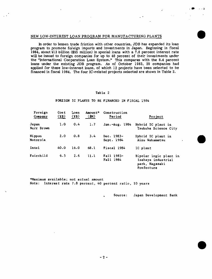
NEW LOW-INTEREST LOAN PROGRAM FOR MANUFACTURING PLANTS
In order to lessen trade friction with other countries, JDB has expanded its loan program to promote foreign imports and investments in Japan. Beginning in fiscal 1984, about ¥13 billion ($55 million) in special loans with a 7.8 percent interest rate win be issued to foreign companies for up to 40 percent of their investments under the "International Cooperation Loan System." This compares with the 8.4 percent loans under the existing JDB program. As of October 1983, 20 companies had applied for these low-interest loans, of which 12 projects have been selected to be financed in fiscal 1984. The four IC-related projects selected are shown in Table 2.
Table 2
FOREIGN IC PLANTS TO BE FINANCED IN FISCAL 1984
Foreign Company
Japan Burr Brown
Nippon Motorola
Intel
Fairchild
Cost (IfB)
I.O
2.0
40.0
6.5
Loan (¥B)
0.4
0.8
16.0
2.6
Amount* ($M)
1.7
3.4
68.1
11.1
Construction Period
Jan.-Aug. 1984
Dec. 1983-Sept. 1984
Fiscal 1984
Fall 1983-Fall 1984
Project
Hybrid IC plant in Tsukuba Science City
Hybrid IC plant in Aizu Wakamatsu
IC plant
Bipolar logic plant in Isahaya industrial park, Nagasaki Prefecture
*Maxiraum a v a i l a b l e ; not ac tua l amount Note: I n t e r e s t r a t e 7.8 percent , 40 percent r a t i o , 10 years
Source: Japan Development Bank
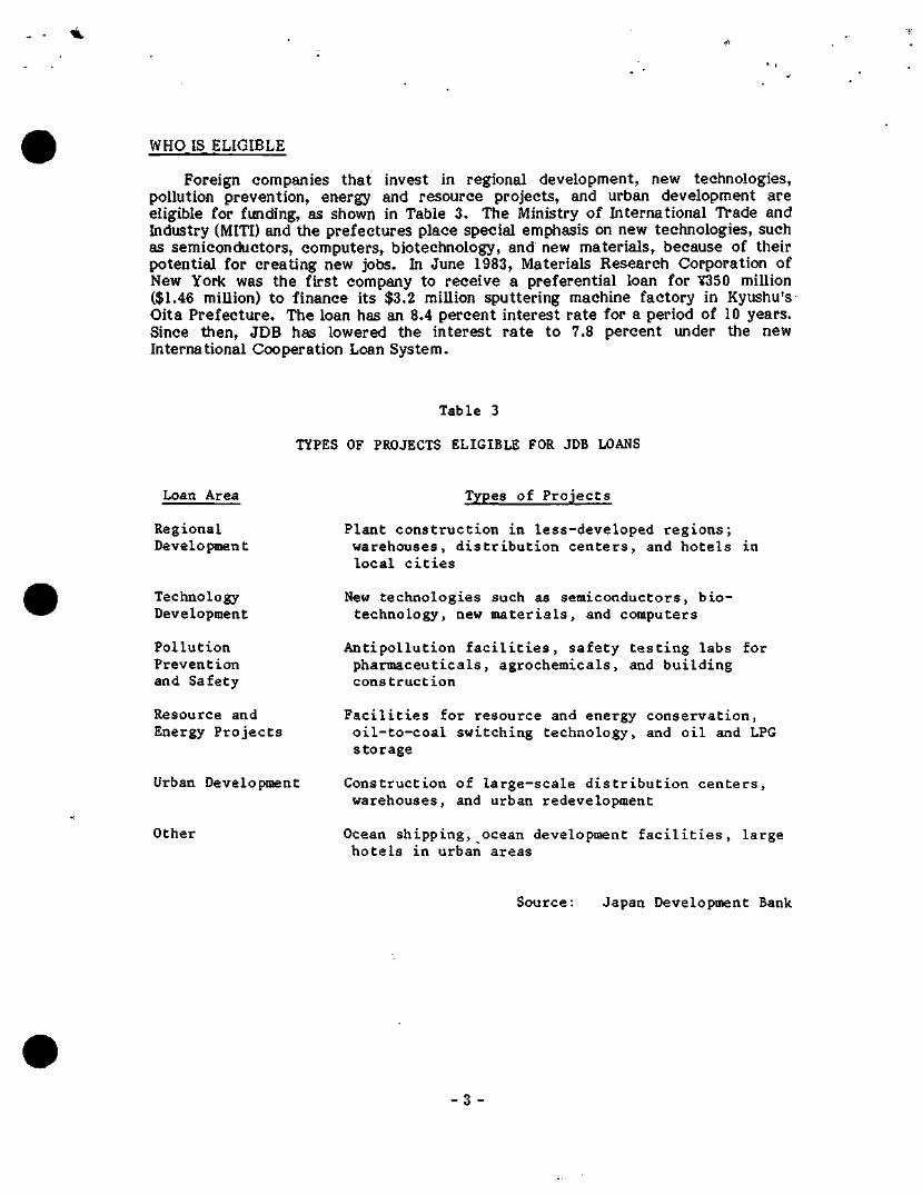
WHO IS ELIGIBLE
Foreign companies that invest in regional development, new technologies, pollution prevention, energy and resource projects, and urban development are eligible for funding, as shown in Table 3. The Ministry of International Trade and Industry (MITI) and the prefectures place special emphasis on new technologies, such as semiconductors, computers, biotechnology, and new materials, because of their potential for creating new jobs. In June 1983, Materials Research Corporation of New York was the first company to receive a preferential loan for ¥350 million ($1.46 million) to finance its $3.2 million sputtering machine factory in Kyushu's Oita Prefecture. The loan has an 8.4 percent interest rate for a period of 10 years. Since then, JDB has lowered the interest rate to 7.8 percent under the new International Cooperation Loan System.
Table 3
TYPES OF PROJECTS ELIGIBLE FOR JDB LOANS
Loan Area Types of P r o j e c t s
Reg iona l Development
P l a n t c o n s t r u c t i o n in l e s s - d e v e l o p e d r e g i o n s ; wa rehouse s , d i s t r i b u t i o n c e n t e r s , and h o t e l s in l o c a l c i t i e s
Technology Development
New t e c h n o l o g i e s such as s e m i c o n d u c t o r s , b i o t e c h n o l o g y , new m a t e r i a l s , and computers
P o l l u t i o n P r e v e n t i o n and Sa fe ty
A n t i p o l l u t i o n f a c i l i t i e s , s a f e t y t e s t i n g l a b s for p h a r m a c e u t i c a l s , a g r o c h e m i c a l s , and b u i l d i n g c o n s t r u c t i o n
Resource and Energy P r o j e c t s
F a c i l i t i e s for r e s o u r c e and energy c o n s e r v a t i o n , o i l - t o - c o a l s w i t c h i n g t e c h n o l o g y , and o i l and LPG S t o r a g e
Urban Development C o n s t r u c t i o n of l a r g e - s c a l e d i s t r i b u t i o n c e n t e r s , w a r e h o u s e s , and urban redeve lopment
Other Ocean shipping, ocean development facilities, large hotels in urban areas
Source: Japan Development Bank
3 -
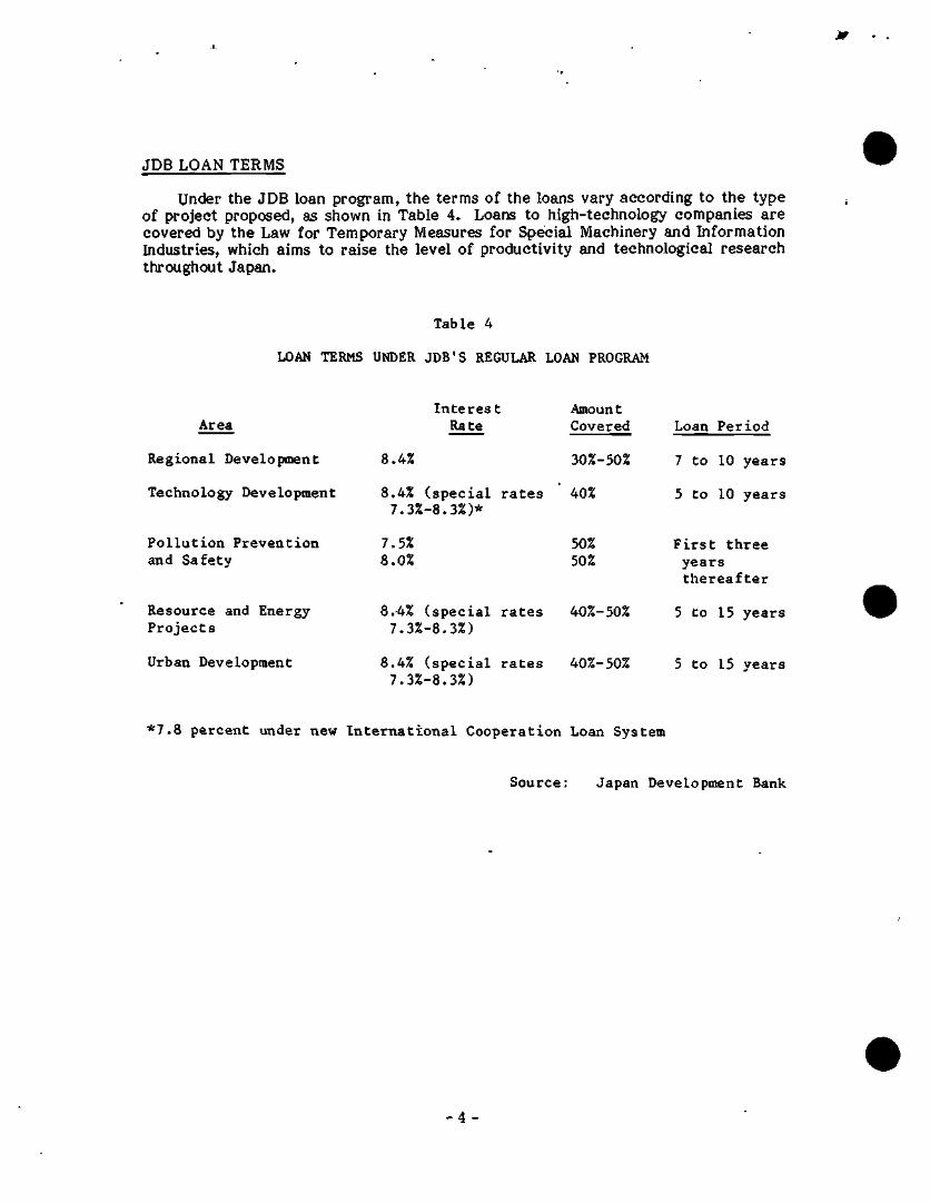
JDB LOAN TERMS
Under the JDB loan program, the terms of the loans vary according to the type of project proposed, as shown in Table 4. Loans to high-technology companies are covered by the Law for Temporary Measures for Special Machinery and Information Industries, which aims to raise the level of productivity and technological research throughout Japan.
Table 4
LOAN TERMS UNDER JDB'S REGULAR LOAN PROGRAM
I n t e r e s t Amount Area Rate Covered Loan P e r i o d
Regiona l Development 8.4% 30%-50% 7 to 10 y e a r s
Technology Development 8.4% ( s p e c i a l r a t e s 40% 5 to 10 y e a r s 7.3%-8.3%)*
Pollution Prevention 7.5% 50% First three and Safety 8.0% 50% years
thereafter
Resource and Energy 8.4% (special rates 40%-50% 5 to 15 years Projects 7.3%-8.3%)
Urban Development 8.4% (special rates 40%-50% 5 to 15 years 7.3%-8.3%)
*7.8 percent under new International Cooperation Loan System
Source: Japan Development Bank
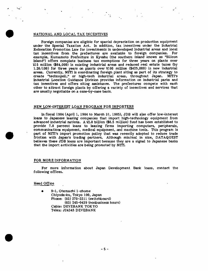
NATIONAL AND LOCAL TAX INCENTIVES
Foreign companies are eligible for specied depreciation on production equipment under the Special Taxation Act. In addition, tax incentives under the Industrial Relocation Promotion Law for investments in undeveloped industrial areas and local tax incentives from the prefectures are available to foreign companies. For example, Kumamoto Prefecture in Kyushu (the southern island known as "Silicon Island") offers complete business tax exemptions for three years on plants over ¥15 miUion ($64,000) in existing industrial areas and reduced real estate taxes (by 1.26/100) for three years on plants over ¥100 million ($425,000) in new industrial areas. Currently, MITI is coordinating foreign plant siting as part of its strategy to create "teehnopoli," or high-tech industrial areas, throughout Japan. MITI's Industrial Location Guidance Division provides information on industrial parks €ind tax incentives and offers siting assistance. The prefectures compete with each other to a t t rac t foreign plants by offering a variety of incentives and services that are usually negotiable on a case-by-case basis.
NEW LQW--INTEREST LOAN PROGRAM FOR IMPORTERS
In fiscal 1984 (April 1, 1984 to March 31, 1985), JDB will also offer low-interest loans to Japanese leasing companies that import high-technology equipment from advanced industrial nations. A ¥2.0 biUion ($8.5 miUion) fund has been established to provide 7.8 percent loans to leasing firms importing computers, peripherals, communications equipment, medical equipment, and machine tools. This program is part of MITI's import promotion policy that was recently adopted to reduce trade friction with Japan's trading partners. Although minimal in size, DATAQUEST believes these JDB loans are important because they are a signal to Japanese banks that the import activities are being promoted by MITI.
FOR MORE INFORMATION
For more information about Japan Development Bank loans, contact the following offices.
Head Office
9-1, Otemachi 1-chome Chiyoda-ku, Tokyo 100, Japan Phone: (03) 270-3211 (switchboard)
(03) 245-0439 (nonbusiness hours) Cable: DEVEBANK TOKYO Telex: J24343 DEVEBANK
Overseas Offices
Washington, D.C. Representative Office 1019 19th Street, N.W., Suite 600 Washington, DC 20036 U.S.A. Phone:(202) 331-8696 Cable: DEVEBANK WASHINGTONDC Telex: 440084 JDBK Ul
New York Representative Office 71 Broadway, Room 306 New York, NY 10006 U.S.A. Phone:(212) 269-0527 Cable: DEVBANKMIN NEWYORK Telex: 421054 KAIGIN
London Representative Office P. <5c O. Building 122-138 Leadenhall Street London EC3V 4PT, United Kingdom Phone: (01) 623-0172, 0173 Cable: JADEBANK LONDON-EC3 Telex: 888907 JDBLDN
Frankfurt Representative Office Rhein Main Center Bockenheimer Landstrasse 51-53 6000 Frankfurt am Main Federal Republic of Germany Phone: (0611) 724341, 724342 Cable: JADEBANK FRANKFURT Telex: 412946 JDBF
Sheridan M. Tatsuno
tyiff) Dataquest i 1 * 4 • • _
EIEJ Code: Newsletters
JAPANESE MARKET OVERVIEW—1982-1983
DATAQUEST's Semiconductor Industry Service held its annual conference in Palm Springs, California, on October 17 through 19, 1983. The conference included presentations by members of DATAQUEST's Semiconductor Group. Gene Norrett, Director of the Japanese Semiconductor Industry Service, presented an overview of the Japanese market.
The presentation covered three major topics:
• The Japanese economy
• The Japanese electronics industry
• DATAQUEST's outlook for the Japanese semiconductor industry
A copy of Mr. Norrett's presentation is attached for your information.
Patricia S. Cox
Copyright ©30 November 1983 Dataquest Incorporated-Reproduction Prohibited
The conteni of this leport represents our interpretai ion and analysts of information generally available lo the puDlic or released tiy responsible individuals in ihe subject companies bul is not gua'anleea as to accuracy or completeness It does not coniain material
provided to us m confidence by our cl ients Individual companies reported on and analyzed by DATAQUEST may be cl ients of this and/or other DATAQUEST services This intormaKon is not furnished >r\ connect ion witt i a sale or of ler to sell securities or in connect ion
* i t h Ihe sol ici tat ion of an oi ler lo Duy securit ies This l i rm and its parent and/or their oMicers stockholders or members of iheir families may (rom time to l ime have a long or short posit ion in the securItIes mentioned and may sell or buy such securItIes
Dataquest Incorporated, A Subsidiary of A.C. Nielsen Company /1290 Ridder Park Drive / San Jose, CA 95131 / (408) 971-9000 / Telex 171973
Dataquest
JAPANESE MARKET OVERVIEW—1982-1983
Gene Norrett Director
Japanese Semiconductor Industry Service Dataquest Incorporated
Mr. Norrett is Director of DATAQUEST's Japanese Semiconductor Industry Service. Prior to joining DATAQUEST, Mr. Norrett spent 14 years with the Motuarola Semiconductor Group, serving in various marketing and management positions. He was most recently Manager of Market Research, where he was responsible for research analysis of worldwide semiconductor industry trends. While at Motorola, he also served as Chairman of the Semiconductor Industry Association's Trade Statistics Committee. His educational background includes a B.A. degree in Mathematics from Temple University and an M.S. degree in Applied Statistics from Villanova University.
Dataquest Incorporated SEMICONDUCTOR INDUSTRY CONFERENCE
October 17-19, 1983 Palm Springs, California
Dataquest Incorporated, A Subsidiary of A.C. Nielsen Company /1290 Bidder Park Drive / San Jose, CA 95131 / (408) 971-9000 / Telex 171973
JAPANESE MARKET OVERVIEW 1982-1983 Gene Norrett
Director - Japanese Semiconductor Industry Service DATAQtJEST Incorporated
Good Morning Ladies and Gentlemen.
I would like to talk to you this morning on three topics: the Japanese economy, its electronics industry and, finally, an overview of our current outlook for its semiconductor industry.
Because of Japan's heavy reliance on its trading partners, the country also suffered frcan the recession which gripped the rest of the world in 1981 and 1982. In fact, Japanese commentators frequently note that: "When the U.S catches a cold, Japan gets pneumonia." The recession hit Japan during the final quarter of calendar year 1981, when the economy recorded its first quarterly decline since the 1975 recession.
In the first quarter of 1983 we saw signs of recovery, which lagged behind the U.S. recovery. In that quarter Japan experienced a real growth rate of 2.8 percent versus a U.S. growth of 2.4 percent. The second quarter has just been announced, at 3.6 percent, good by some standards but substantially less than the U.S.'s explosive 9.2 percent.
Going back to 1982 for a moment, we believe that the decline in Japan's GNP was largely due to a sharp decline in the export sector since domestic demand had already been weak since early 1980 and it has remained that way through 1981 and 1982. Net external demand (that is, exports minus imports) was the mainstay of Japanese economic growth during much of 1980 and 1981. During these years exports rose 30.7 and 13.9 percent, respectively, on a yen basis. Then in 1982 the growth of e:q>orts dropped to only 2.7 percent causing serious production and marketing dislocations throughout the economy. These dislocations plus the serious growing deficit problem has government officials thoroughly perplexed.
National bankruptcy is not a term outsiders would use to describe the Japanese state; however this term is becoming common among Japanese bureaucrats and businessmen to describe the huge budget deficits. The need for tax structure reforms is evident and these have been a major goal of Prime Minister Nakasone and his two predecessors. Despite the weakness of the economy in 1982, government expenditures have continued to grow. The result has been a pervading sense of crisis over the public debt and an increasing sense of frustration over how to deal with it.
-1-
Copyright © 17 October 1983 Dataquest Incorporated-Reproduction Prohibited
Dataquest Incorporated, A Subsidiary of A.C. Nielsen Company /1290 Ridder Park Drive / San Jose, CA 95131 / (408) 971-9000 / Telex 171973
The nation's deficit in fiscal 1982 was $45.02 billion and was 3.8 percent of the GNP. Although down slightly from 1981, it is still too high. Amazingly it is a higher percentage than the U.S. deficit, which was 3.2 percent of GNP or $42.9 billion.
To finance this deficit the government has resorted to bond issues, which were first made in 1975. Before then the government only issued construction bonds which were primarily used to finance infrastructure projects such as roads, bridges and harbors. Deficit bond issues have accelerated to the point that they have exceeded construction bond issues.
The current slowdown in the Japanese economy has called into question the feasibility of former Prime Minister Suzuki's original pledge of eliminating deficit financing bonds in fiscal 1984. We believe that the Nakasone government will have to increase taxes and continue issuing deficit bonds beyond fiscal 1984.
Moreover, growing U.S. pressure for increased Japanese defense spending is further frustrating the government and creating debates among the predominantly pacifist population. The principal reason for this U.S. insistence is the fact that, although Japan is the second leading western industrial power behind the U.S., it is fourth in defense spending behind the U.S., West Germany, O.K. and France. We believe that Japan will increase defense spending but fall short of levels suggested by the other western powers. A major constraint though is Article 9 of the Japanese constitution which limits defense spending to 1 percent of the GNP.
On the balance of trade scene, Japan's trade friction with its major trading partners seems to have eased considerably, due to the government's recent agreements to curb exports of cars and video tape recorders to the U.S. and Western Europe. However, the U.S. trade representatives still maintain that Japan has given its industry an advantage over other countries by supporting basic R&D and promoting exports.
When we look at Japan's historic trade balance with its three major partners - the United States, Western Europe and South East Asia - we see some very striking trends. First, Japan's total trade with the United States - imports plus exports - grew from $40 billion to $60 billion between 1978 and 1982. However, there was a decline in 1982 - the first such decline since 1975. Second, Japan's balance of trade with the United States climbed frcsn a $1 billion deficit in 1975 to a $12 billion surplus in 1982. This rapid rise has triggered the Reagan administration policy makers to develop three "hard-line" approaches:-
-2-
Copyright©17 October 1983 Dataquest Ihcorporated-Reproduction Prohibited
Dataquest Incorporated, A Subsidiary of A.C. Nielsen Company /1290 Bidder Park Drive / San Jose, CA 95131 / (408) 971-9000 / Telex 171973
• First, criticism of Japan's industrial policy, including allegations of product dumping and targeting by key high growth industries
• Second, pressure to open public corporations such as Nippon Telegraph and Telephone, and strategic industries, such as semiconductors
• Third, to encourage the Japanese government to liberalize capital markets in order to promote appreciation of the yen
Regarding the last two approaches we have observed that Japanese tariffs on industrial goods are now on the average comparable or below those of the United States and the EEC. Secondly, there appears to be a political commitment to increase the liberalization process, as evidenced in these steps:
• April 1983 - MITI sent 30 represented to the United States, New York, Chicago, Los Angeles, San Francisco, to encourage industrial siting.
• August 1983 - They have established a low interest rate financing systan with $55 million for 12 projects in Fiscal 1984. Of these 12 projects, the following companies have been involved:
Nippon Motorola Intel Japan Fairchild Japan Burr Brown Japan
• September 1983 - They have created a reliability center in Japan to inspect products and issue quality guarantee certificates.
• September 1983 - They will exchange aggregated sales data of the top 12 integrated circuit manufacturers with the department of commerce, and finally
f April 1984 - They have agreed to the elimination of tariffs on semiconductors.
While not all of these approaches will bear fruit in the first year, we believe that they will help reduce trade frictions between the two countries.
-3-
Copyright © 17 October 1983 Dataquest Incorporated-Reproduction Prohibited
Dataquest Incorporated, A Subsidiary of A.C. Nielsen Company / 1290 Ridder Park Drive / San Jose, CA 95131 / (408) 971-9000 / Telex 171973
Next, looking at Japanese trade with Western Europe, we observe the following trends:
• Between 1975 and 1982 total trade rose from $12 billion to a little over $33 billion.
• Japan's trade surplus with Western Europe was $13 billion -versus $12 billion with the United States.
• The European deficit has been growing at a compound annual rate of 26.6 percent.
• European imports into Japan have been essentially flat since 1979.
These alarming statistics have been fodder for protectionist sentiment in Europe. In February 1983, European countries imposed quotas on Japanese VTRs in an attempt to help their own producers, which are trailing far behind. However, quotas alone will not suffice. Increased Japanese investment in Europe will be required in order to reduce trade frictions. Through March 1982, Japanese investments in Europe totaled $5.3 billion, of which $1.0 billion was invested in manufacturing.
Finally we have observed that the level of trade between Japan and Southeast Asia neighbors is significantly higher than with either the U.S. or Western Europe. At the end of 1982, total trade was $67 billion, up frcan $23 billion in 1975. Also you will note that Japan's very low trade deficit even declined slightly in 1982.
Now, for a moment, let's turn our attention to the electronics industry which has been the main engine for Japan's economic growth.
Until the late 1970s, Japan sought to catch up with the technological superiority of the West. The much touted VLSI Project (1976-79) is a dramatic example of MITI's determined effort to achieve superiority in dynamic RAMs.
By the early 1980's however, Japan had achieved parity with the West in many technical fields such as robotics, ceramics, advanced computers and new semiconductor elements. Instead of copying and improving technology from the West, Japan has been forced to innovate. In 1980, MITI issued its famous "Visions for the igSOs" which sets out its goal of creating an information-based society. Fourteen high-technology industries have been selected for development.
-4-
Copyright © 1 7 October 1983 Dataquest Incorporated-Reproduction Prohibited
Dataquest Incorporated, A Subsidiary of A.C. Nielsen Company /1290 Bidder Park Drive / San Jose, CA 95131 / (408) 971-9000 / Telex 171973
In order to develop these industries, MITI and NTT have structured a three-pronged strategy consisting of the following:
• Joint R&D projects involving government, industry and universities
• Infrastructure development
• Venture capital infusion
By coordinating these programs, MITI hopes to catalyze technological innovation in various regions of Japan which are now suffering from the decline in the mature heavy equipment industries.
Joint R&D Programs
MITI's plan for the 1980s consists of a set of joint government/industry R&D programs running on parallel tracks.
Undoubtedly you have already heard of the 5th generation computer project, which is the centerpiece of Japan's high-technology strategy. However, that is only part of the story. As you can see, MITI has initiated several other projects organized in a manner similar to the VLSI project. Total government funding for these projects will be around $1.4 billion. This does not include corporate funding, which may equal or exceed this amount.
In addition, NTT is developing a nationwide telecommunications network, called the Information Network System (INS). Total estimated procurement costs for this system will be $120 billion during the next 20 years (or $6 billion dollars per year)for system investments.
One of the least publicized aspects of the Japanese R&D programs is the fierce competition between MITI and NTT. For example, NTT surpassed MITI in the development of a Japanese-to-English and English-to-Japanese computerized language translator. Incidentally, this was one of MITI's major goals of the fifth generation project, which will be discussed shortly.
Briefly, I would like to summarize the goals and research themes of each of these MITI and NTT projects.
-5-
Copyright © 1 7 October 1983 Dataquest Incorporated-Reproduction Prohibited
Dataquest Incorporated, A Subsidiary of A.C. Nielsen Company /1290 Ridder Park Drive / San Jose, CA 95131 / (408) 971-9000 / Telex 171973
• 5th Generation Computer - The main purpose is to develop an artificial intelligence computer using parallel processing with a large knowledge based system. To a novice a knowledge based system ccMnbines current technology systems with new inference systems. According to Tohru Motooka, Tokyo University Professor of Electrical Engineering and Chairman of this project (ICOT), the hardware design of the sequential machine will be completed by the end of 1983. Total funding will be about $450 million.
• Supercomputer - The purpose is to design a high-speed computer for scientific and technological uses which will be able to perform 10 billion floating point operations per second, i.e. 10 gigaflops. The key semiconductor research areas include gallium arsenide (GaAs), Josephson Junctions, and high electron mobility transistors (HEMT). The current state of the art production machine is Hitachi's HITAC 5-81, which operates at 630 megaflops. Total funding for the Supercomputer project will be about $105 million.
• Next Generation Industries - In October 1981, the Long-Term Industrial Technology Planning Committee, a study group of academics and experts commissioned by MITI, issued a report recommending basic research essential for establishing new industries that are expected to flourish in the 1990s. These industries include biotechnology, aerospace, information processing, alternative energies, and ocean development. Three general fields were chosen by MITI for development: new materials (such as high polymers, ceramics, and composite materials), biotechnology, and new semiconductor function elements. The total funding is projected to be $473 million.
• New Semiconductor Function Elements - A portion of the Next Generation Industries Project is the New Semiconductor Function Element Project, Japan's next step in developing basic semiconductor technology. The overall goal of the project is to extend the geometric design and durability of integrated circuits. Ten companies have organized themselves into the Research and Development Association for Future Electronics Devices, which is being commissioned to conduct basic research. Project expenses will be covered by MITI consignment payments and patents will be made available through the Industrial Technology Promotion Agency. The total cost of the project is expected to run about $114 million.
-6-
Copyright © 17 October 1983 Dataquest Incorporated-Reproduction Prohibited
Dataquest Incorporated, A Subsidiary of A.C. Nielsen Company /1290 Ridder Park Drive / San Jose, CA 95131 / (408) 971-9000 / Telex 171973
• Integrated Network System - The last and potentially the largest development program to be discussed in this sequence is the Nippon Telegraph and Telephone Integrated Network System (INS). NTTs INS program aims to develop a nationwide digital syst:em for telephone network, data and FAX services using fiber optics and satellite broadcasting.
Infrastructure Development
The key to Japan's strategy for dominance in high-technology fields is the Technopolis Concept, which is a plan aimed at establishing new tech cities throughout the country. Tsukuba, which is 60 miles northeast of Tokyo, is the first of these cities and will be quite a show piece when it is completed.
Moreover, these new cities are programmed to have populations of more than 200,000 and would consist of research institutes, schools, housing, and recreational facilities clustered around new high-technology industries. It is further planned that they would be within one-day travel frcsn Tokyo, Osaka, or Nagoya, by plane or bullet train.
The Industrial Location and Environment Protection Board of MITI is currently screening 19 candidate sites for the new Technopolis cities. The overall project is being directed by the Technopolis '90 Construction Concept Committee, an advisory board to MITI. Cities designated as Technopolis centers will receive central government financing, public works projects, tax benefits, and MITI and JETRO guidance.
Venture Capital
The third pillar of Japan's new industrial strategy is to provide venture capital to start-up firms. This strategy has long been utilized by the West to stimulate new ventures. Generally, DATAQUEST has observed the following trends in Japanese venture capital activities:
• Source of venture capital are large banks, securities companies, and trading houses.
• Six of the largest venture capital firms are not private, but are owned by huge conglomerates such as Mitsubishi Bank, Nomura Securities, and the Dai-Ichi Kangyo Bank.
-7-
Copyright © 17 October 1983 Dataquest Incorporated-Reproduction Prohibited
Dataquest Incorporated, A Subsidiary of A.C. Nielsen Company /1290 Ridder Park Drive / San Jose, CA 95131 / (408) 971-9000 / Telex 171973
• Venture capital firms are proliferating in Japan - BUT not for the purposes consistent with MITI goals of high-technology development. Few of these companies want to insure risk capital involved in leading edge technology, but are investing in more secure industries such as retailing, wholesaling, and consumer manufacturing.
• Japanese venture capital firms spread their portfolio about 70 percent in loans and 30 percent in equity stocks.
• Most loans go to relatively mature companies preparing to go public.
• Japanese entrepreneurs are reluctant to forfeit part of the ownership of their companies to outside firms - this is why most venture capital is in the form of loans rather than equity.
• Typical start ups are especially reluctant to allow foreign investment in their companies, either directly or through venture capitalist.
• Legal guidelines in Japan state that venture capital firms may not place a director on the board of a company they invest in (unlike the U.S.) and they may own no more than 49 percent of a company.
Semiconductor
Finally I want to turn your attention to the semiconductor industry in Japan. When I first came to DATAQUEST to start the Japanese Semiconductor Industry Service last October and started to look into this industry, I became aware very quickly that on the surface there was considerable distrust and misunderstanding. However, as I looked closer, what I saw was entirely different.
First, from the factory siting we noted the following activities.
U.S. Companies in Japan
Company Activities
Texas Instruments 3 factories. Motorola 1 factory, 1 planned Intel Design Center and factory planned Fairchild factory planned Burr Brown factory planned IBM 1 factory Analog Devices 1 factory Intel Rectifier 1 factory Other U.S. and European companies have marketing with some final testing.
-8-
Coj^right © 1 7 October 1983 Dataquest Incorporated-Reproduction Prohibited
Dataquest Incorporated, A Subsidiary of A.C. Nielsen Company /1290 Ridder Park Drive / San Jose, CA 95131 / (408) 971-9000 / Telex 171973
Japanese Companies in the West
NEC 4 factories, California and Scotland Hitachi 2 factories, Texas and West Germany Toshiba 1 factory in California Fujitsu 1 factory in California Mitsubishi 1 factory planned in N. Carolina Other Japanese companies have Marketing with some final testing.
Next from a joint venture and licensing perspective we have observed a very rapid rise in this activity since 1980. By our calculation there were 4 in 1980, 6 in 1981, and 10 in 1982. Through June of this year it has grown to 13. At this rate we could see over 20 joint ventures and licensing agreements between U.S. and Japanese companies for 1983.
We believe there are two reasons for this growth.
1. In December 1980, Japan revised the Foreign Exchange and Trade Control law, which loosened MITI's control over joint ventures.
2. The proliferation of microprocessor and peripheral applications has forced many Japanese manufacturers to form partnerships with the U.S. leaders in order to develop their own expertise. The following figure shows just the licensing agreements that currently exist today:
Impact of VLSI Project on Equipment Manufacturers
One of the least discussed outcomes of the VLSI Project is its impact on U.S. semiconductor equipment manufacturers. Besides the 64K DRAM, the project sought to develop process technologies for eventual use in IM, 4M and ultimately 16M bit DRAMs. Key VSLI manufacturing innovations include:
High-speed E-beam drawing unit for IM bit devices. It draws a 1 square centimeter device in 9 to 15 minutes.
High performance dry etching machine
E-beam software system
Laser scanning LSI analyzing system
Infrared scanning IC thermo distribution measuring system
Ultra-high-speed pattern generator with 300 mHz speed
-9-
Copyright © 17 October 1983 Dataquest Incorporated-Reproduction Prohibited
Dataquest Incorporated, A Subsidiary of A.C. Nielsen CoInpany /1290 Bidder Park Drive / San Jose, CA 95131 / (408) 971-9000 / Telex 171973
After the VLSI project ended, these patents were sold to Japanese manufacturers who are currently developing automated equipment.
U.S. manufacturers are responding in several ways:
• Signing joint ventures with Japanese manufacturers to gain entry or increase presence in the Japanese market. Since 1981, there have been 20 joint ventures in semiconductor fab equipment
• Opening manufacturing plants in Japan (e.g. MRC)
Next I want to discuss the semiconductor market. First, right up front, I want to say that 1983 will be a good year for the industry. The year started out with the market being driven principally by office automation and factory automation products. But as consumer end equipment inventories wore down due to an inproving export market demand, production of products such as VTRs, video disks and color TVs began to increase and we now have a market condition that is similar to what you have heard about the U.S. from Fred Zieber.
As of June 1983, new order rates for semiconductors were up an average of 28 percent ahead of the fourth quarter, with office automation leading the pack. The office automation market is currently seeing demand up 58 percent over the fourth quarter levels. Currently there is a shortage of 64K DRAMS, EPROMs, 8-bit microcontrollers D to A and A to D converters, laser diodes and TTL. The shortage of TTL is so acute that Nissho-Iwai Co. Limited, a major trading company, imported $300,000 worth of TTL frcan the U.S.S.R. in July. This chart shows our quarterly forecast for consumption through the fourth quarter of 1984.
Our analysis and forecast shows a resurgence of the industry in the second and third quarters of 1983, with a continual building quarter-to-quarter through 1984. We believe that the backlogs that are currently being built will be translated into solid shipments and end consumption for at least the next six quarters.
Our forecast calls for discretes to grow about 12 percent this year and 13 percent in 1984. For integrated circuits we see 29 percent in 1983 and 32 percent growth next year.
The principal reasons for assuming that 1984 will be a good year for semiconductor consumption in Japan are as follows:
-10-
Copyright © 1 7 October 1983 Dataquest Incorporated-Reproduction Prohibited
Dataquest Incorporated, A Subsidiary of A.C. Nielsen Company /1290 Ridder Park Drive / San Jose, CA 95131 / (408) 971-9000 / Telex 171973
The 1984 Olympics will precipitate sales of all types of consumer electronics.
U.S. presidential elections will take place in 1984 and we can expect the U.S. econony to be "dressed" for the ritual.
Japanese 256K DRAM production will be ramped from 800 thousand units in 1983, to 10 million units in 1984, and 64K DRAM production will grow fr«n 208 million units in 1983 to 420 million in 1984.
The Japanese government will act to stimulate capital investment in 1983, which will pay dividends in 1984 in terms of industrial electrcmics, such as telecoiranuncations, and all forms of office and factory automation products.
Summary
In summary, first I have talked about an economy that is debt ridden but one that shows every sign of being able to cope and in fact achieve more than a 3 percent real growth rate this year.
Second, we have observed an electronics industry that is embarking on a "take lead" path, one that is certainly very costly and will no doubt be successful in some but not all of its endeavors.
Third, we see a very healthy semiconductor industry, one that has every sign of achieving and in fact bettering our projection of 24 percent growth in yen for 1983.
Finally, we have seen a multitude of trade barrier breaking moves on both sides of the Pacific which will only breed a strengthening of the world semiconductor suid electrcHiics industry.
Thank you.
-11-
Copyright © 17 October 1983 Dataquest Incorporated-Reproduction Prohibited
Dataquest Incorporated, A Subsidiary of A.C. Nielsen Company /1290 Bidder Park Drive / San Jose, CA 95131 / (408) 971-9000 / Telex 171973
JAPAN REAL CNP GROWTH RATE SEASONALLY ADJUSTED AT ANNUAL RATE
1980 1981 1982 1983
Source; Internationa) Monetary Fund DATAQUEST
lU O
Ul
a. - 5 -
-10
REAL GNP GROWTH RATE SEASONALLY ADJUSTED AT ANNUAL RATE — U.S. AND JAPAN
1980
JAPAN
1982
UNITED STATES'
Source: International Monetary Fund DATAQUEST
- 12 -
Copyright ©17 October 1983 Dataquest Incorporated-Reproduction Prohibited
Dataquest Incorporated, A Subsidiary of A.C. Nielsen Company /1290 Ridder Park Drive / San Jose, CA 95131 / (408) 971-9000 / Telex 171973
• ' » . . '
JAPANt nevENUc t u r
OOVERNtUEKT DEBT ISSUES
S CONSmUCTKHI BONDS
•l^rafNll^ ^ ^ s ^ _ • s ^ I i I ^ Hi
- » -e
» r i n T l « W » T T 7 1 7 1 « l H t J ' 1 3 -
- DEVISED BUDGET • BUDGET ESTIIUTt „„^ , u _ . 9
1982 DEFENSE SPENDING
(Billions of Dollars)
0) K
3 ^ 0 0 11.
0 (0
z 0 3 -1 0
KWU -
150-
100-
50-
I -~i JAPAN FRANCE U.K. W. GERtMANY U.S.
Soum: DATAQUESrr
- 13 -
Copyright © 1 7 October 1983 Dataquest Incorporated-.Repreduction Prohibited
Dataquest Incorporated, A Subsidiary of A.C. Nielsen Company /1290 Ridder Parl< Drive / San Jose, CA 95131 / (408) 971-9000 / Telex 171973
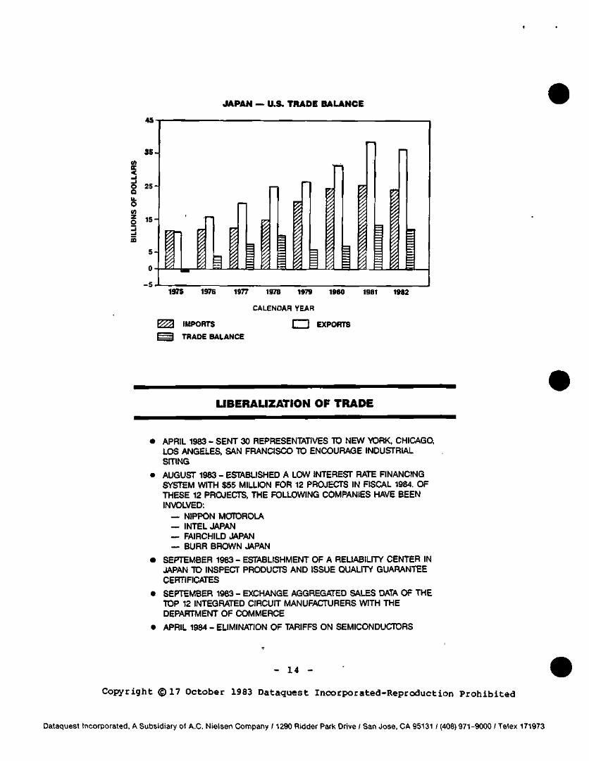
JAPAN — U.S. TRADE BALANCE
45
ss~ (0 EC < O 25 a
V) z o _l - I ffi
15'
5-
-5-L
f i
i_i
P I i
I J 197S 197E 1977 1978 1979 19S0 1981 1982
CALENDAR YEAR
^ IMPORTS C H EXPORTS
^ 5 TRADE BALANCE
LIBERALIZATION OF TRADE
• APRIL 1983 - SENT 30 REPRESENTATIVES TD NEW YORK, CHICAGO, LOS ANGELES, SAN FRANCISCO TD ENCOURAGE INDUSTRIAL SITING
• AUGUST 1983 - ESTABLISHED A LOW INTEREST RATE FINANCING SYSTEM wr rn $55 M ILLION FOR 12 PROJECTS IN F ISCAL 1984. O F THESE 12 PROJECTS, THE FOLLOWING COMPANIES HAVE BEEN INVOLVED:
— NIPPON MCfTDROLA — INTEL JAPAN — F A I R C H I L D JAPAN
— BURR BROWN JAPAN
• SEPTEMBER 1983 - ESTABLISHMENT OF A RELIABILrTY CENTER IN JAPAN TD INSPECT PRODUCTS AND ISSUE QUALITY GUARANTEE CERTIFICATES
• SEPTEMBER 1983 - EXCHANGE AGGREGATED SALES DATA OF THE TOP 12 INTEGRATED CIRCUIT MANUFACTURERS WITH THE DEPARTMENT OF COMMERCE
• APRIL 1984 - ELIMINATION OF TARIFFS ON SEMICONDUCTORS
- 14 -
Copyright ©17 October 1983 Dataquest Incorporated-Reproduction Prohibited
Dataquest Incorporated, A Subsidiary of A.C. Nielsen Company /1290 Ridder Park Drive / San Jose, CA 95131 / (408) 971-9000 / Telex 171973
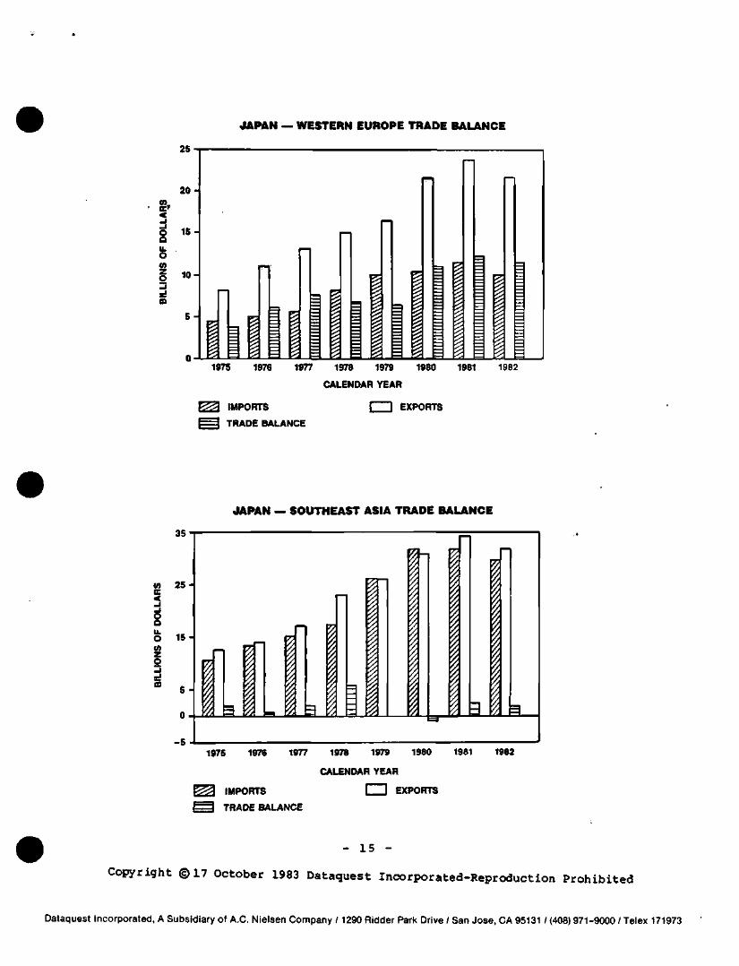
JAPAN — WESTERN EUROPE TRADE BALANCE
25
20 -
S' < •i O 15 o IL . o m § 10
5 -
^ F5
t ^ bd fc^
s;
1 ^
%
K =
1975 1976 1977 1978 1979 1980 1981
CALENDAR YEAR
19B2
F^^ IMPORTS
^ ^ TRADE BALANCE
I I EXPORTS
JAPAN — SOUTHEAST ASIA TRADE BALANCE
35
w 25 cc < -1
o o O 15 -M z o
0 - L P
L I I
I 1975 1976 1977 1978 1979 1980
CALENDAR YEAR
^ 3 IMPORTS [ m EXPORTS
^ 3 TRADE BALANCE
1981 1382
- 15 -
Copyright © 1 7 October 1983 Dataquest Incorporated-Repreduction Prohibited
Dataquest Incorporated, A Subsidiary of A.C. Nielsen Company /1290 Bidder Park Drive / San Jose, CA 95131 / (408) 971-9000 / Telex 171973
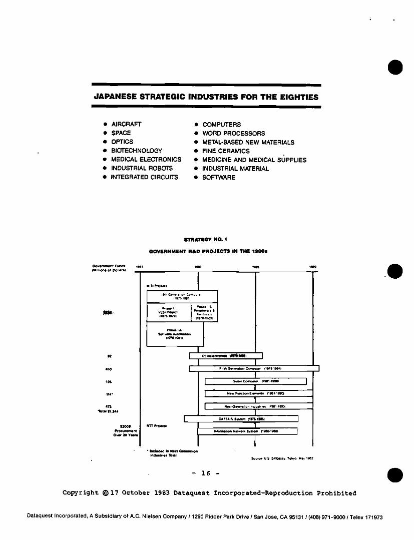
JAPANESE STRATEGIC INDUSTRIES FOR THE EIGHTIES
• AIRCRAFT
• SPACE • OPTICS
• BIOTECHNOLOGY • MEDICAL ELECTRONICS
• INDUSTRIAL ROBCn-S
• INTEGRATED CIRCUITS
• COMPUTERS • W O R D PROCESSORS
• METAL-BASED NEW MATERIALS • FINE CERAMICS
• MEDICINE AND MEDICAL SUPPLIES • INDUSTRIAL MATERIAL
• SOFTWARE
STRATEGY NO. 1
GOVERNMENT R&D PROJECTS IN THE 19S0s
Govammeni Funds (Mllltons of Dollars)
62
450
472
Total SI .344
S200B Procuremont
Ov*r 20 Ytars
4Th GtnvffEiOfi COTi urer
VLSI P'Oracl JlST6-tfl7Ul
Phiat llG PfnpncTBis (
T^rrfiin^ij M 979-1^3!
PtlAH ILA Soriwiri Auiorrialibn
n^T^iSeii
I I DT^itmecTroma* ti#rt^it(wi
FJMH G«nernion Computer |1979 l99 i l
&UptI CaiTlQLJiCT (TH1-I»t}l
N«w Function Elements (1981 1990)
Ntit-&Eiier*liqn mOuSirm <^9aM99Q|
I NTT ProIKIt
CAPTAIN irifvr, ^^97t•^Ui\
I Information Network Svstem (19BD-t9SS)
' Included in Neit Gonoratlon Industries Total
Source US Emt>assy, Tokyo May 1962
- 16
Copyright ©17 October 1983 Dataquest Incorporated-Reproduction Prohibited
Dataquest Incorporated, A Subsidiary of A.C. Nielsen Company /1290 Bidder Park Drive / San Jose, CA 95131 / (408) 971-9000 / Telex 171973
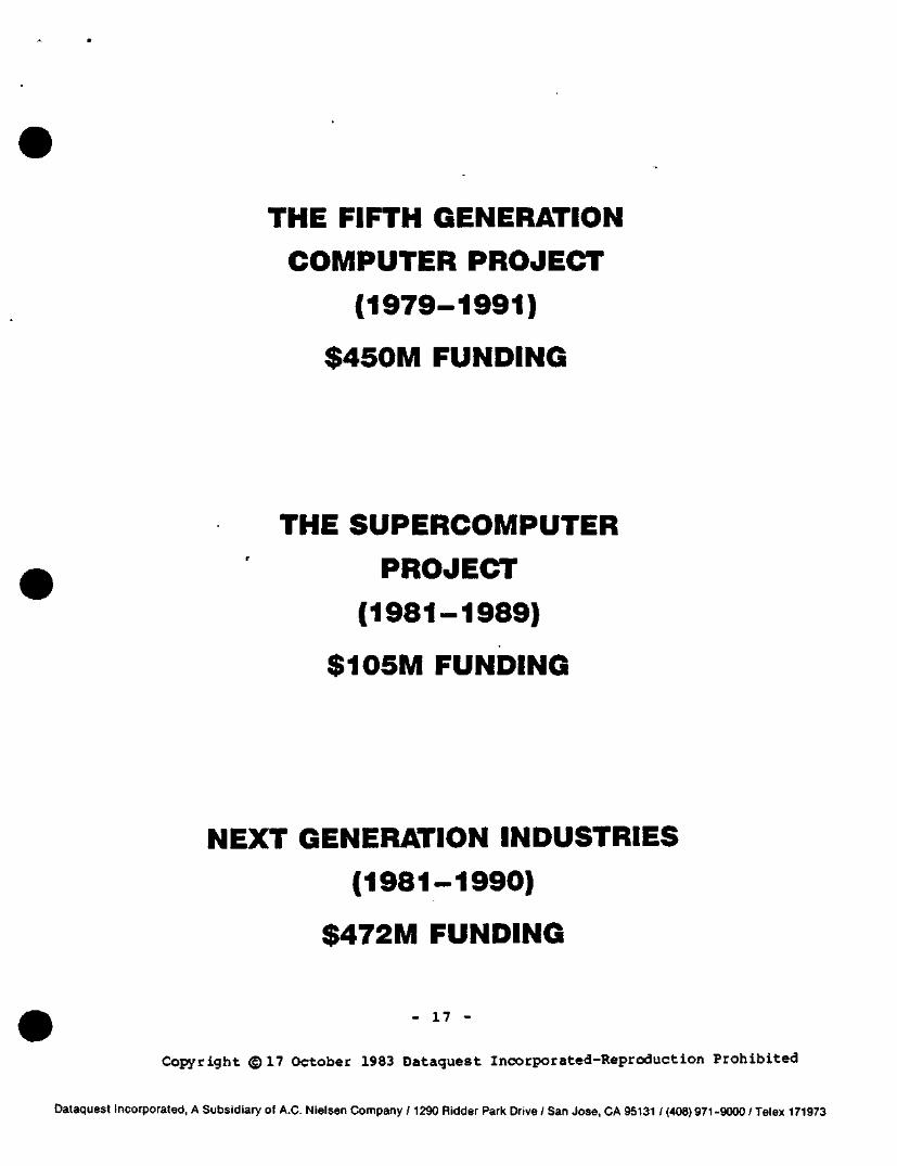
THE FIFTH GENERATION
COMPUTER PROJECT
(1979-1991)
$450M FUNDING
THE SUPERCOMPUTER
PROJECT
(1981-1989)
$105M FUNDING
NEXT GENERATION INDUSTRIES
(1981-1990)
$472M FUNDING
- 17 -
Copyright © 1 7 October 1983 Dataquest Incorporated-Reproduction Prohibited
Dataquest Incorporated, A Subsidiary of A.C. Nielsen Company /1290 Ridder Park Drive / San Jose, CA 95131 / (408) 971-9000 / Telex 171973
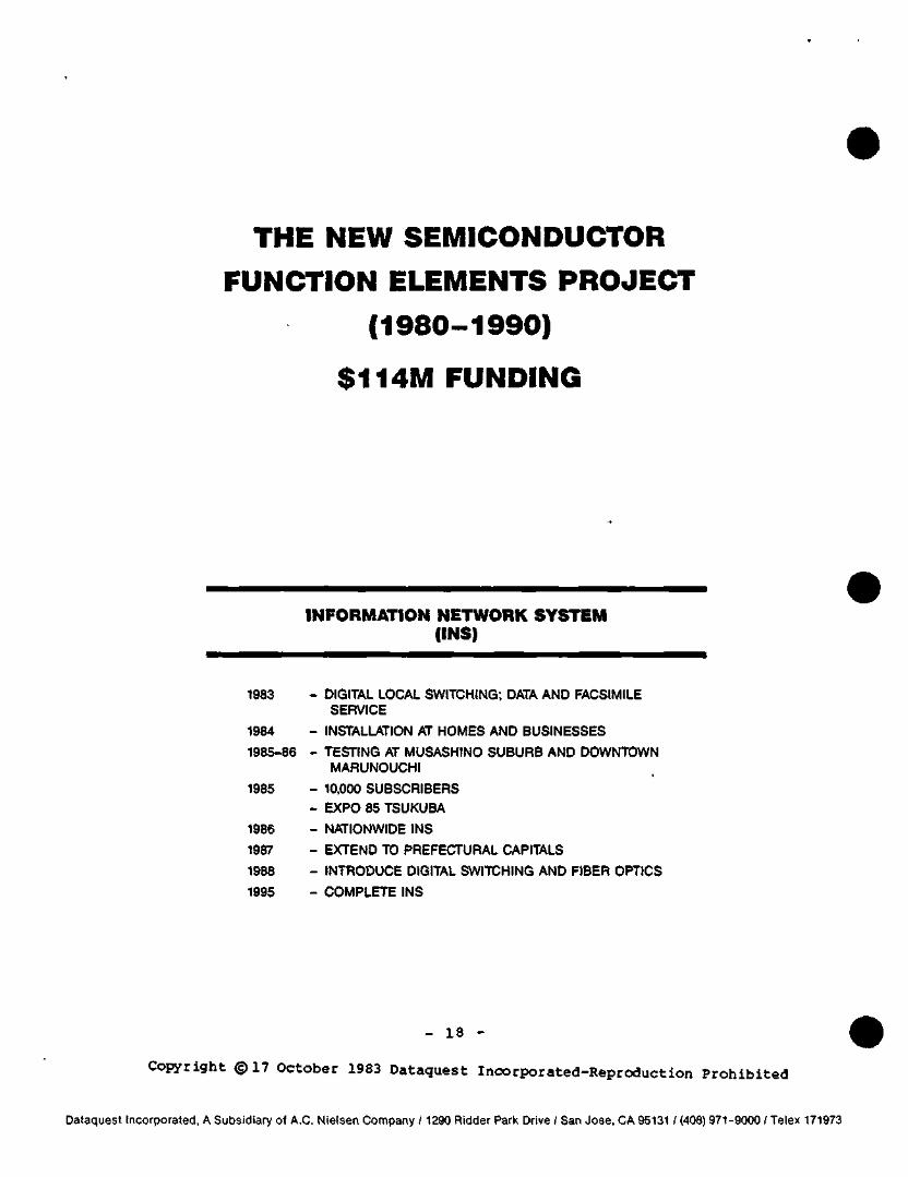
THE NEW SEMICONDUCTOR
FUNCTION ELEMENTS PROJECT
(1980-1990)
$114M FUNDING
INFORMATION NETWORK SYSTEM (INS)
1983 - DIGITAL LOCAL SWITCHING; DATA AND FACSIMILE SERVICE
1984 - INSTALLATION AT HOMES AND BUSINESSES
1985-86 - TESTING AT MUSASHINO SUBURB AND DOWNTOWN MARUNOUCHI
1985 - 10,000 SUBSCRIBERS - E X P O 85 TSUKUBA
1986 - NATIONWIDE INS
1987 - EXTEND TO PREFECTURAL CAPITALS
1988 - INTRODUCE DIGITAL SWITCHING AND FIBER OPTICS
1995 - COMPLETE INS
- 18 -
Copyright ©17 October 1983 Dataquest Incorporated-Reproduction Prohibited
Dataquest Incorporated, A Subsidiary of A.C. Nielsen Company /1290 Ridder Park Drive / San Jose, CA 95131 / (408) 971-9000 / Telex 171973
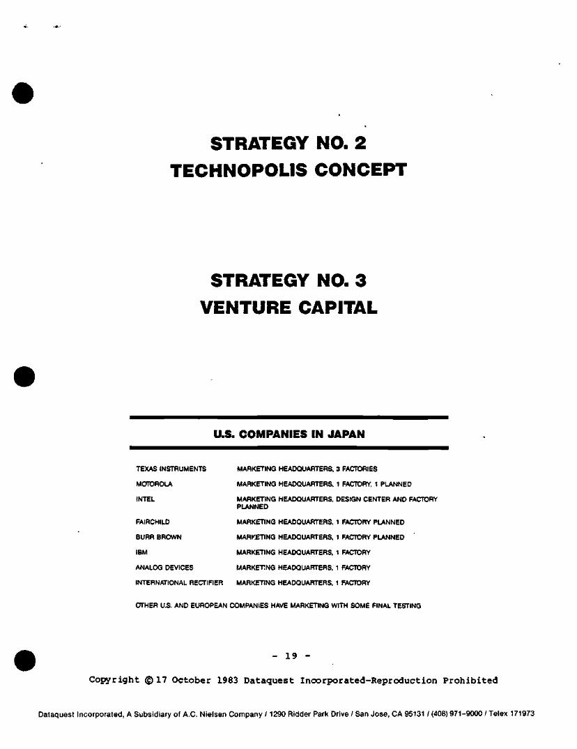
STRATEGY NO. 2
TECHNOPOLIS CONCEPT
STRATEGY NO. 3
VENTURE CAPITAL
U.S. COMPANIES IN JAPAN
TEXAS INSTRUMENTS MARKETING HEAOOUARTERS, 3 FACTORIES
MOTOROLA MARKETING HEADQUARTERS, 1 FACTORY, 1 PLANNED
INTEL MARKETING HEADQUARTERS, DESIGN CENTER AND FACTORY PLANNED
FAIRCHILD MARKETING HEADQUARTERS. 1 FACTORY PLANNED
BURR BROWN MARKETING HEADQUARTERS, 1 FACTORY PLANNED
IBM MARKETING HEADQUARTERS, 1 FACTORY
ANALOG DEVICES MARKETING HEADQUARTERS, 1 FACTORY
INTERNATIONAL RECTIFIER MARKETING HEADQUARTERS, 1 FACTORY
OTHER U.S. AND EUROPEAN COMPANIES HAVE MARKETING WITH SOME FINAL TESTING
- 19 -
Copyright © 1 7 October 1983 Dataquest Incorporated-Reproduction Prohibited
Dataquest Incorpora ted, A Subsidiary of A .C. N ielsen Company / 1 2 9 0 Ridder Park Drive / San Jose, CA 95131 / (408) 971-9000 / Telex 171973
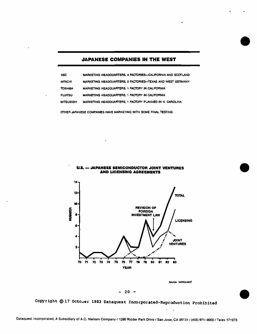
JAPANESE COMPANIES IN THE WEST
NEC MARKETING HEADQUARTERS, 4 FACTORIES—CALIFORNIA AND SCOTLAND
HITACHI MARKETING HEADQUARTERS. 2 FACTORIES—TEXAS AND WEST GERMANY
TOSHIBA MARKETING HEADQUARTERS, 1 FACTORY IN CALIFORNIA
FUJITSU MARKETING HEADQUARTERS, 1 FACTORY IN CALIFORNIA
MITSUBISHI MARKETING HEADQUAFaERS, 1 FACTORY PLANNED IN N. CAROLINA
OTHER JAPANESE COMPANIES HAVE MARKETING WITH SOME FINAL TESTING
U.S. — JAPANESE SEMICONDUCTOR J O I N T VENTURES A N D U C E N S I N Q AGREEMENTS
14-1
TOTAL
LICENSING
N
/ JOINT / VENTURES
YEAR
Source: DATAQUEST
- 20 -
Copyright © 1 7 Octc^er 1983 Dataquest Incorporated-Reproduct ion Prohibited
Dataquest Incorporated, A Subsidiary of A.C. Nielsen Company /1290 Ridder Park Drive / San Jose, CA 95131 / (408) 971-9000 / Telex 171973
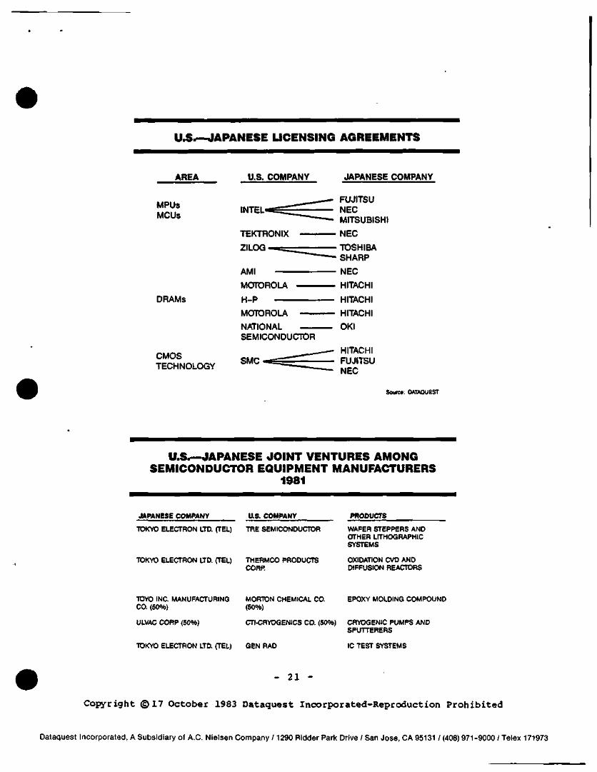
U.S.—JAPANESE LICENSING AGREEMENTS
AREA U.S. COMPANY JAPANESE COMPANY
MRUs
MCUs
DRAMs
CMOS
TECHNOLOGY
INTEL-
TEKTRONIX
ZILOG'
AMI
MOTOROLA
H-P
MOTOROLA
NATIONAL
SEMICONDUCTOR
SMC
FUJITSU
NEC
MITSUBISHI
NEC
•TOSHIBA
SHARP
NEC
HITACHI
HITACHI
HITACHI
OKI
HITACHI
FUJITSU
NEC
Source: DATAQUEST
U.S^—JAPANESE JOINT VENTURES AMONG SEMICONDUCTOR EQUIPMENT MANUFACTURERS
1981
JAPANESE COMPANY U.S. COMPANY
TOKYO ELECTRON LTD. (TEL) TRE SEMICONDUCTOR
TOKYO ELECTRON LTD. (TEL) THERMCO PRODUCTS CORP.
PRODUCTS
WAFER STEPPERS AND OTHER LrrnOGHAPHIC SYSTEMS
OXIDATION CVD AND DIFFUSION REACTORS
TOYO INC. MANUFACTURING MORTON CHEMICAL CO. EPOXY MOLDING COMPOUND CO. (50%) (50%)
ULVAC CORP (50%)
TOKYO ELECTRON LTD. (TEL) GEN RAD
CTI-CRYOGENICS CO. (50%) CRYOGENIC PUMPS AND SPUTTERERS
IC TEST SYSTEMS
- 21 -
Copyright © 1 7 October 1983 Dataquest Incorporated-Reproduction Proh ib i ted
Dataquest Incorporated, A Subsidiary of A.C. Nielsen Company /1290 Ridder Park Drive / San Jose, CA 95131 / (408) 971-9000 / Telex 171973
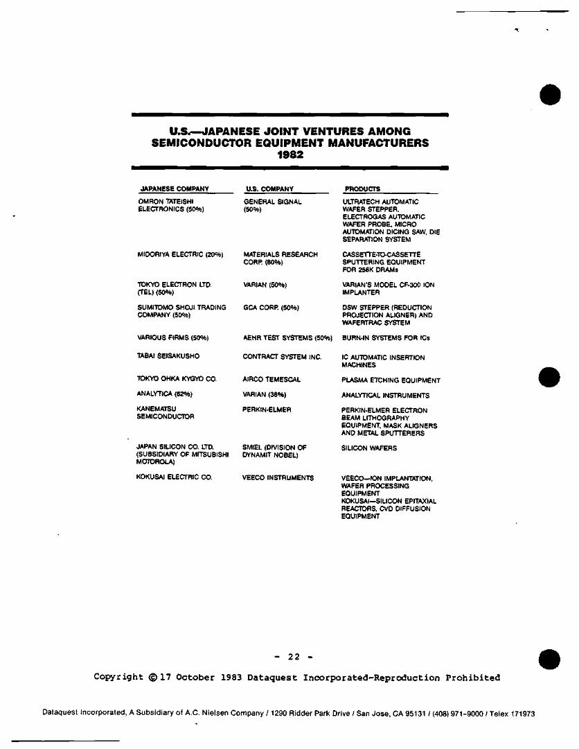
U.S.—JAPANESE JOINT VENTURES AMONG SEMICONDUCTOR EQUIPMENT MANUFACTURERS
1982
JAPANESE COMPANY
OMRON TATEISHI ELECTRONICS (50%)
MIDORIYA ELECTRIC (20%)
TOKYO ELECTRON LTD, (TEL) (50%)
SUMITOMO SHOJI TRADING COMPANY (50%)
VARIOUS FIRMS (50%)
TABAI SEISAKUSHO
TOKYO OHKA KYGYO CO.
ANALYTICA (62%)
KANEMATSU SEMICONDUCTOR
JAPAN SILICON CO. LTD, (SUBSIDIARY OF MITSUBISHI MOTOROLA)
KOKUSAI ELECTRIC CO.
US . COMPANY PRODUCTS
GENERAL SIGNAL (50%)
MATERIALS RESEARCH CORR (80%)
VARIAN (50%)
GCA CORR (50%)
AEHR TEST SYSTEMS (50%)
CONTRACT SYSTEM INC.
AIRCO TEMESCAL
VARIAN (36%)
PERKIN-ELMER
SMIEL (DIVISION OF DYNAMIT NOBEL)
VEECO INSTRUMENTS
ULTRATECH AUTOMATIC WAFER STEPPER, ELECTROGAS AUTOMATIC WAFER PROBE. MICRO AUTOMATION DICING SAW, DIE SEPARATION SYSTEM
CASSETTE-TO-CASSETTE SPUTTERING EQUIPMENT FOR 256K DRAMs
VARIAN'S MODEL CF-300 ION IMPLANTER
DSW STEPPER (REDUCTION PROJECTION ALIGNER) AND WAFERTRAC SYSTEM
BURN-IN SYSTEMS FOR ICs
iC AUTOMATIC INSERTION MACHINES
PLASMA ETCHING EQUIPMENT
ANALYTICAL INSTRUMENTS
PERKIN-ELMER ELECTRON BEAM LITHOGRAPHY EQUIPMENT, MASK ALIGNERS AND METAL SPUTTERERS
SILICON WAFERS
VEECO—ION IMPLANTATION, WAFER PROCESSING EQUIPMENT KOKUSAI—SILICON EPITAXIAL REACTORS, CVD DIFFUSION EQUIPMENT
- 22 -
Copyright ©17 October 1983 Dataquest Incorporated-Reproduction Prohibited
Dataquest Incorporated, A Subsid iary of A.C. Nielsen Company / 1290 Ridder Park Drive / San Jose, CA 95131 / (408) 971-9000 / Telex 171973
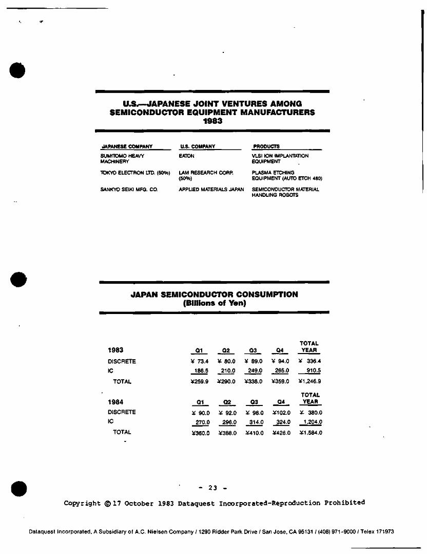
U.S^-JAPANESE JOINT VENTURES AMONG SEMICONDUCTOR EQUIPMENT MANUFACTURERS
1983
JAPANESE COMPANY
SUMITOMO HEAVY MACHINERY
TOKYO ELECTRON LTD. (50%)
SANKYO SEIKI MFG. CO.
U.S. COMPANY PRODUCTS
EATON
LAM RESEARCH CORR (50%)
APPLIED MATERIALS JAPAN
VLSI ION IMPLANTATION EQUIPMENT
PLASMA ETCHING EQUIPMENT (AUTO ETCH 480)
SEMICONDUCTOR MATERIAL HANDLING ROBOTS
JAPAN SEMICONDUCTOR CONSUMPTION (Billions of Yen)
1983
DISCRETE
IC
TOTAL
1984 DISCRETE
IC
TOTAL
01
¥ 73.4
186.5
¥259.9
01
X 90.0
270.0
¥360.0
02
¥ 80.0
2100
¥290.0
Q2_
¥ 92.0
296.0
¥388.0
03
¥ 89.0
249.0
¥338.0
Q3
¥ 96.0
3140
¥410.0
Q4
¥ 94.0
265.0
¥359.0
Q4
¥1020
324.0
¥426.0
TOTAL YEAR
¥ 336.4
910.5
¥1,246.9
TOTAL YEAR
¥: 380.0
1,204.0
¥1,584.0
- 23 -
Copyright © 1 7 October 1983 Dataquest Incorporated-Reproduction Prohibited
Dataques t Incorporated , A Subsidiary of A.C. Nie lsen Company / 1 2 9 0 Ridder Park Drive / San Jose, CA 95131 / (408) 971-9000 / Te lex 171973
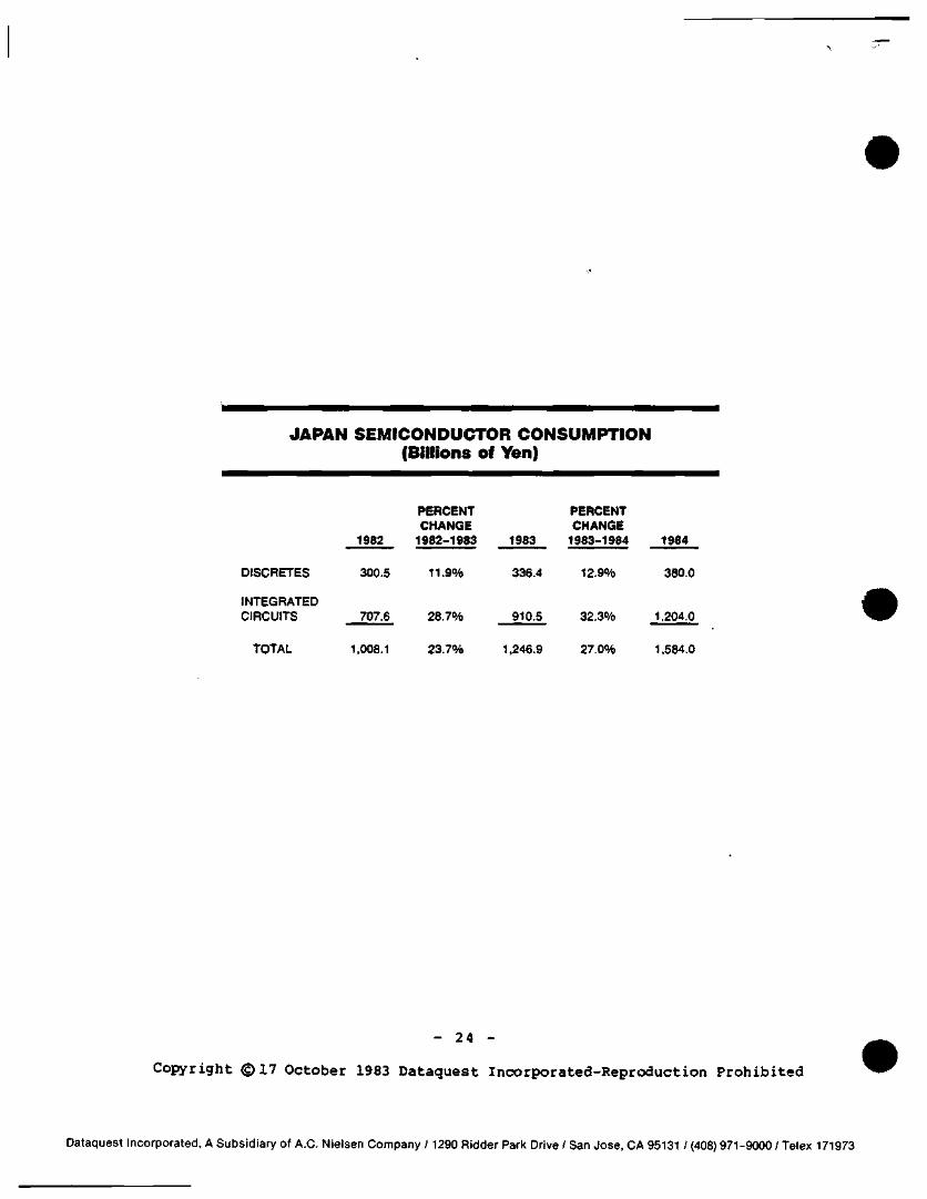
JAPAN SEMICONDUCTOR CONSUMPTION (Billions of Yen)
DISCRETES
INTEGRATED CIRCUITS
TOTAL
PERCENT CHANGE
1982 1982-1983
300.5
707.6
11.9%
28.7%
1983
336.4
910.5
PERCENT CHANGE
1983-1984 1984
12.9
32.3%
1,008.1 23.7% 1,246.9 27,0%
380.0
1.204.0
1,584.0
- 24 -
Copyright © 1 7 October 1983 Dataquest Incorporated-Reproduction Proh ibited
Dataquest Incorporated, A Subsidiary of A.C. Nielsen Company /1290 Bidder Park Drive / San Jose, CA 95131 / (408) 971-9000 / Telex 171973
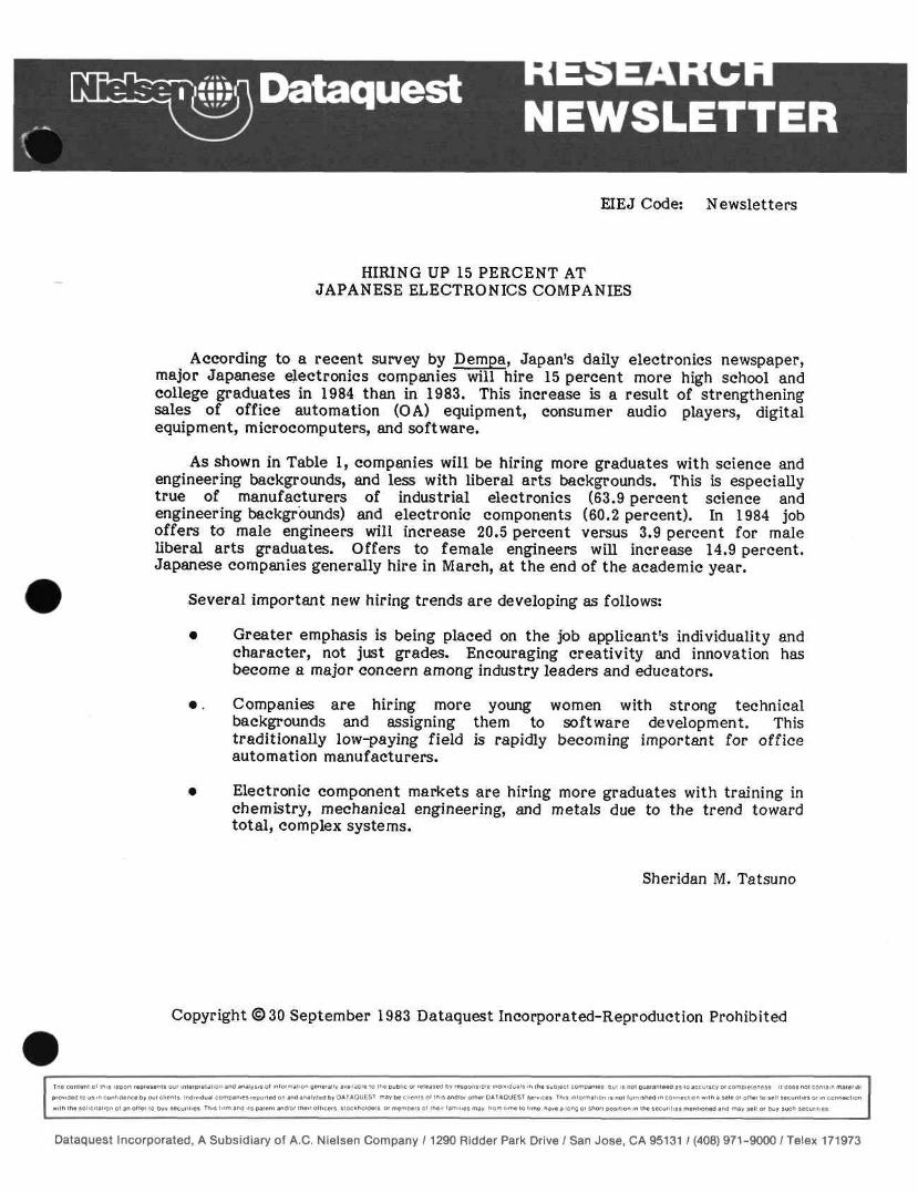
Dataquest J *-'^< ^w * • • i Aid ~
EIEJ Code: Newsletters
HIRING UP 15 PERCENT AT JAPANESE ELECTRONICS COMPANIES
According to a recent survey by Dempa, Japan's daily electronics newspaper, major Japanese electronics companies will hire 15 percent more high school and college graduates in 1984 than in 1983. This increase is a result of strengthening sales of office automation (OA) equipment, consumer audio players, digital equipment, microcomputers, and software.
As shown in Table 1, companies will be hiring more graduates with science and engineering backgrounds, and less with liberal arts backgrounds. This is especially true of manufacturers of industrial electronics (63.9 percent science and engineering t)ackgrbunds) and electronic components (60.2 percent). In 1984 job offers to male engineers will increase 20.5 percent versus 3.9 percent for male liberal arts graduates. Offers to female engineers will increase 14.9 percent. Japanese companies generally hire in March, at the end of the academic year.
Several important new hiring trends are developing as follows:
• Greater emphasis is being placed on the job applicant's individuality and character, not just grades. Encouraging creativity and innovation has become a major concern among industry leaders and educators.
• . Companies are hiring more young women with strong technical backgrounds and assigning them to software development. This traditionally low-paying field is rapidly becoming important for office automation manufacturers.
• Electronic component markets are hiring more graduates with training in chemistry, mechanical engineering, and metals due to the trend toward total, complex systems.
Sheridan M. Tatsuno
Copyright ©30 September 1983 Dataquest Incorporated-Reproduction Prohibited
Trie content ol ihIs report represents our mlerpcelation and analysts ol in lormai ion generally available lo me pub l ic or released by responsiDle individuals in the subject companIes but is not guaranteed as lo accuracy or completeness it does noi contain material
provided lo us m conf idence by our cl ients Individual companies reported on and analyzed by DATAQUEST may be cl ients ol this and/or other DATAQUEST services This mlormat ion is not furnished in connection with a sale or olter to sell securit ies or m connect ion
with the sol ici tat ion of an offer TO buy securit ies Tfiis f irm ana its parent and/or their ot i icers stockholders or mernbers of their lamii ies may trom time to time have a long or short posItIon m the securit ies mentioned and rnay sell or buy such securit ies
Dataquest Incorporated, A Subsidiary of A.C. Nielsen Company /1290 Ridder Park Drive / San Jose, CA 95131 / (408) 971-9000 / Telex 171973
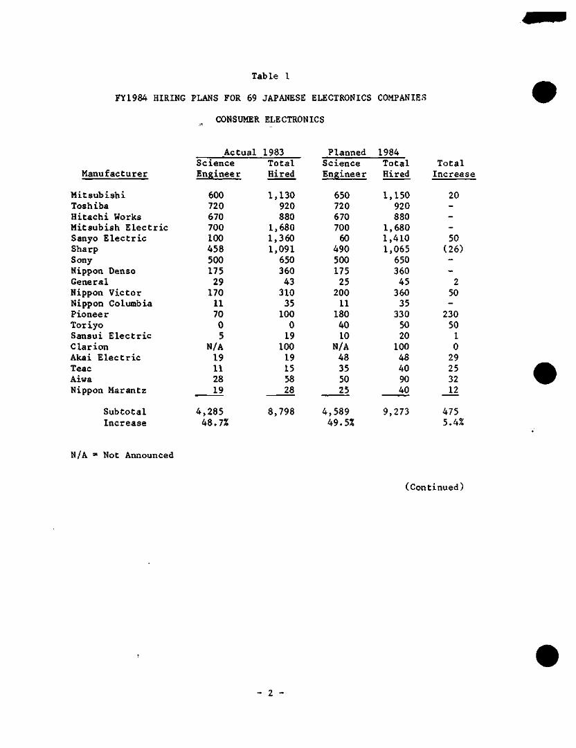
Table 1
FY1984 HIRING PLANS FOR 69 JAPANESE ELECTRONICS COMPANIES
CONSUMER ELECTRONICS
Manufacturer
Mitsubishi Toshiba Hitachi Works Mitsubish Electric Sanyo Electric Sharp Sony Nippon Denso General Nippon Victor Nippon Columbia Pioneer Toriyo Sansui Electric Clarion Akai Electric Teac Aiwa Nippon Marantz
Subtotal Increase
Actual Science Engineer
600 720 670 700 100 458 500 175 29 170 11 70 0 5
N/A 19 11 28 19
4,285 48.7%
1983 Total Hired
1,130 920 880
1,680 1,360 1,091 650 360 43 310 35 100 0 19 100 19 15 58 28
8,798
Planned Science Engineer
650 720 670 700 60
490 500 175 25 200 11 180 40 10
N/A 48 35 50 25
4,589 49.5%
1984 Total Hired
1,150 920 880
1,680 1,410 1,065 650 360 45 360 35 330 50 20 100 48 40 90 40
9,273
Total Increase
20 ---50 (26) --2 50 -230 50 1 0 29 25 32 12
475 5.4%
N/A = Not Announced
(Continued)
- 2 -
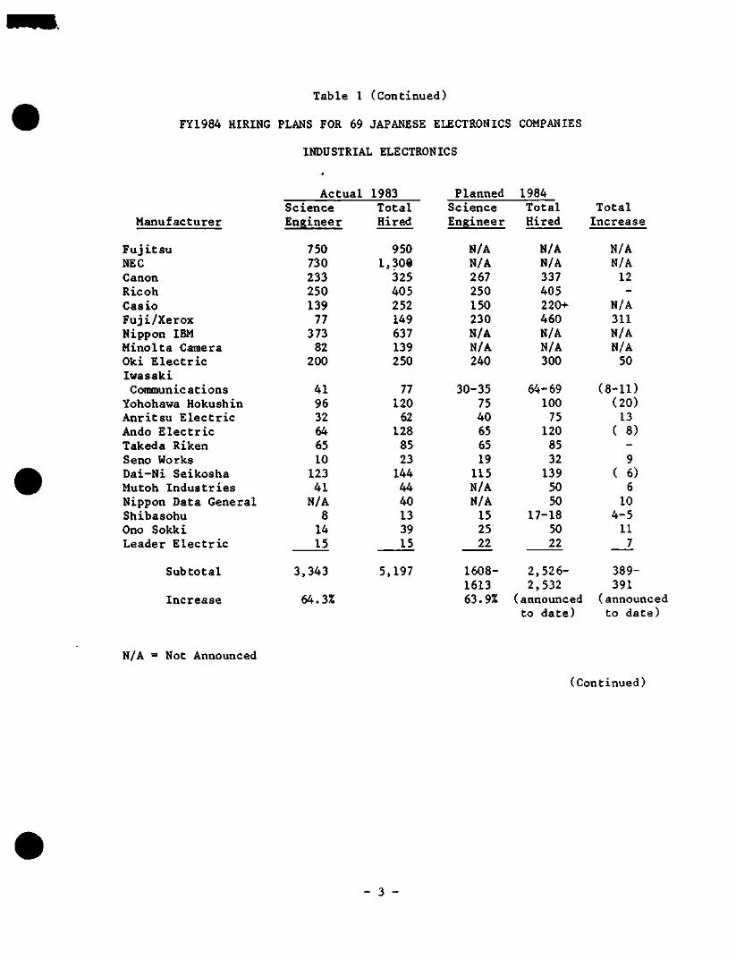
Table 1 (Continued)
FY1984 HIRING PLANS FOR 69 JAPANESE ELECTRONICS COMPANIES
INDUSTRIAL ELECTRONICS
Manufacturer
Fujitsu NEC Canon Ricoh Casio Fuji/Xerox Nippon IBM Minolta Camera Oki Electric Iwasaki Communications Yohohawa Hokushin Anritsu Electric Ando Electric Takeda Riken Seno Works Dai-Ni Seikosha Mutoh Industries Nippon Data General Shibasohu Ono Sokki Leader Electric
Subtotal
Increase
Actual Science Engineer
750 730 233 250 139 77 373 82 200
41 96 32 64 65 10 123 41 N/A 8 14 15
3,343
64.3%
1983 Total Hired
950 1,309 325 405 252 149 637 139 250
77 120 62 128 85 23 144 44 40 13 39 15
5,197
Planned 1984 cience ngineer
N/A N/A 267 250 150 230 N/A N/A 240
30-35 75 40 65 65 19 115 N/A N/A 15 25 22
1608-1613 63.9%
Total Hired
N/A N/A 337 405 220+ 460 N/A N/A 300
64-69 100 75 120 85 32 139 50 50
17-18 50 22
2,526-2,532
(announced to date)
Total Increase
N/A N/A 12 -
N/A 311 N/A N/A 50
(8-11) (20) 13 ( 8) -9
( 6) 6 10
4-5 11 7
389-391
(announced to date)
N/A = Not Announced
(Continued)
- 3
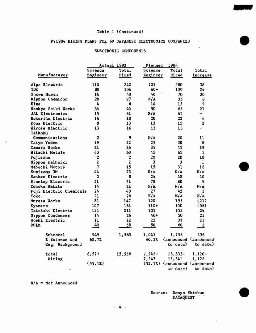
Table 1 (Continued)
FY1984 HIRING PLANS FOR 69 JAPANESE ELECTRONICS COMPANIES
ELECTRONIC COMPONENTS
Manufacturer
Alps Electric TDK Showa Musen Nippon Chemicon Elna Sankyo Seiki Works JAL Electronics Hokuriku Electric Kowa Electric Hirose Electric Teikoku Communications Taiyo Yuden Tamura Works Hitachi Metals Fujisohu Nippon Kaiheiki Mabuchi Motors Sumitomo 3M Sanken Electric Stanley Electric Tohoku Metals Fuji Electric Chemicals Toko Murata Works Kyocera Tateishi Electric Nippon Condenser Hoshi Electric ROLM
Subtotal % Science and Eng. Background
Total Hiring
Actual Science Engineer
110 80 16 20 4 34 15 16 8 13
2 19 21 40 2 2 7 44 2 51 14
I 24 21 81 107 131 14 11 40
949 60.7%
1983 Total Hired
242 106 40 27 6 44 61 18 13 16
9 22 26 60 2 2 15 73 8 71 21 40 26 147 161 211 26 12 58
1,563
Planned Science Engineer
125 60+ 40 N/A 10 50
N/A 20 13 13
N/A 23 35 45 20 3 15
N/A 24 70
N/A 27
N/A 120 110+ 105 40+ 25 50
1,045 60.2%
1984 Total Hired
280 130 70 35 15 65 61 22 15 16
20 30 45 65 20 3 31
N/A 48 80 N/A 42 N/A 195 150 155 50 33 60
1,736 (announced to date)
Total Increase
38 24 30 8 9 21 -4 2 -
11 8 19 5 18 1 16
N/A 40 9
N/A 2
N/A (21) (56) 24 21 21 2
256 (announced to date)
8,577 15,558 7,242- 13,535- 1,120-7,247 13,541 1,122
(55.1%) (53.5%) (announced (announced to date) to date)
N/A = Not Announced
Source: Dempa Shimbun DATAQUEST
- 4 -
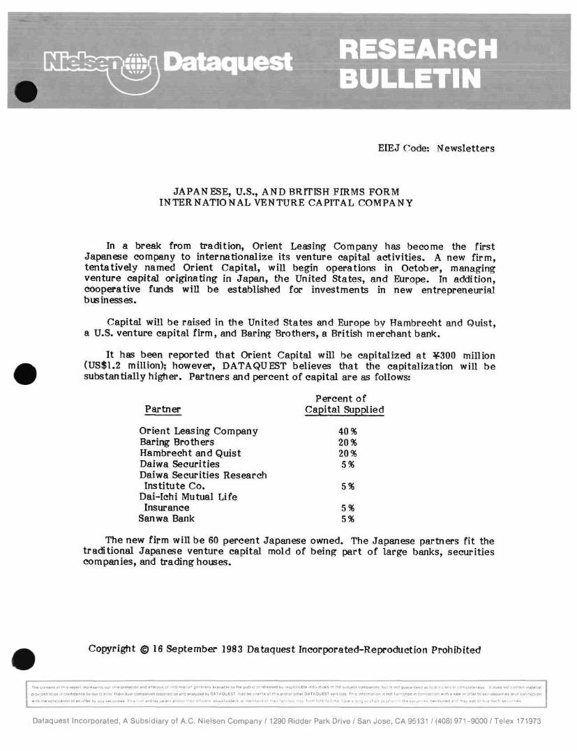
EIEJ Code: Newsletters
JAPANESE, U.S., AND BRITISH FIRMS FORM INTERNATIONAL VENTURE CAPITAL COMPANY
In a break from tradition, Orient Leasing Company has become the first Japanese company to internationalize its venture capital activities. A new firm, tentatively named Orient Capital, will begin operations in October, managing venture capital originating in Japan, the United States, and Europe. In addition, coopCTative funds wiU be established for investments in new entrepreneurial businesses.
Capital will be raised in the United States and Europe by Hambrecht and Ouist, a U.S. venture capital firm, and Baring Brothers, a British merchant bank.
It has been reported that Orient Capital will be capitalized at ¥300 million (US$1.2 million); however, DATAQUEST believes that the capitalization will be substantially higher. Partners and percent of capital are as follows:
Partner
Orient Leasing Company Baring Brothers Hambrecht and Quist Daiwa Securities Daiwa Securities Research Institute Co.
Dai-Ichi Mutual Life Insurance
Sanwa Bank
Percent of Capital Supplied
40% 20% 20% 5%
5%
5% 5%
The new firm will be 60 percent Japanese owned. The Japanese partners fit the traditional Japanese venture capital mold of being part of large banks, securities companies, and trading houses.
Copyright © 16 September 1983 Dataquest Incorporated-RefM-oduction Prohibited
The conien
proviided 1o
wI ih ihe so
1 ol ihi
u s i n c c
ic I ia l io
report represents our inierprelat ian and anal
nddence by our c l ienis indiviOtjal companies
, „ i a n „ l l e . . „ U u , > e . u , „ . = > T r „ > i , „ - „ „ a „
SIS ot in lormai ion generally availatiie io the public or released by respc
epoited on and analyzed by DATAQUEST may be cl ienis ol ihis and/or c
parenl and/or Ihe.r ol l .cers s lock^p ldsrs or rr^E^r^bers oi ii-.e.: (a:..:!i^s
nsible individuals in the subject companies
ther DATAQUEST services This tnlormai io
,^,,, , . o ^ , . ^ e l o l . . e h . v c . ! o . g o r - o r
, b u l
n i s n
•^o.
s n
O i l
:C.
01 guaranteed as
rnished m conn
irMh.esecuntie
to a
ectio
rr.er
curacy or CO
n w i t h a s a l e
I ior .sdana rp
Tipleteness
s r o d e r t o s e l
ay sell •sr bu
It does nol contain material
securit ies or in connection
such securi i jes
Dataquest Incorporated, A Subsidiary of A.C. Nielsen Company / 1290 Ridder Park Drive / San Jose, CA 95131 / (408) 971-9000 / Telex 171973
The types of firms that Orient Capital will invest in are not yet known. Traditionally, Japanese venture capital has gone to relatively mature companies that are engaged in relatively established fields such as retailing, wholesaling, and consumer goods. In contrast to the United States, Japanese venture capital usually has not favored high-technology industries; however, DATAQUEST believes that Orient Capital, with its U.S. and British partners, intends to break with this tradition and invest in high-technology start-ups.
Patricia S. Cox
- 2
Dataquest ^cofTipanyul I f Jc n u 11 gc'flr;i(ii,i u t I Coi [K» 11 iim
RESEARCH BULLETIN
JSIS Code: Newsletters 1985-1986, JSIA
1986-52
JAPANESE INDUSTRIAL ELECTRONICS PRODUCTION FORECAST AT ¥12.5 TRILLION IN FY 1990
SUMMARY
Japanese industrial electronics production will reach ¥12.5 trillion ($74.8 billion)in fiscal 1990, achieving an 11.9 percent compound annual growth rate (CAGR) from fiscal 1985 to fiscal 1990, according to a forecast compiled recently by the Electronic Industries Association of Japan (EIAJ).
INDUSTRIAL ELECTRONICS
Based on the assumption that industrial electronics production in fiscal 1986 will be ¥7,761.3 billion ($46.5 billion), EIAJ forecasts that it will reach ¥12,489.6 billion ($74.8 billion) in fiscal 1990. The CAGR is expected to maintain a level of 11.9 percent for the next five years, a slowdown from the 17.5 percent CAGR of the past five years.
Computers and related electronic data processing equipment are expected to lead the way in substantially raising industrial electronics production. These areas are forecast to grow at a 16.9 percent CAGR. EIAJ expects a surge in demand for large-scale mainframes and networked workstations.
Also worthy of note is the forecast for production of computers and other related electronic data processing equipment, which are expected to reach ¥7.7 trillion ($46.1 billion) in fiscal 1990 and rise to 61.7 percent of total industrial electronics production.
Table 1 shows the EIAJ forecast in detail.
0 © 1986 Dataquest Incorporated December--Reprocluction Prohibited
I The conlent o( ihis repon represenls our mlerpfelalion and analysis ol mlormalion generally available lo Ihe puWic or released by responsible Individuals m Ihe subjeci companIes but Is nol guaranteed as lo accuracy or completeness It does no! conlain
I msterIal prnvirien to us m conlidencp Hy our clients Ind'vidual comnames rRoorted on and analyzed by HAIAOUFST may be clients ol ttiis and/or other DATAQUEST services This information is nol furnished in conneclon with a sale or ofler to sel' securilIes
1 or in connectIor; with the sdicitalion of an offer to buy securities ThiS drm and .Is parent and/or ihciI officers slockholders or rriemt-ers of the r lamIhes may 'rom Dine to lime have a long o' short posilion in ifie sec:untIes menhoned ana may sell or buy such securities
Dataquest Incorporated, 1290 Ridder Park Drive, San Jose, CA 95131-2398, (408) 971-9000, Telex 171973
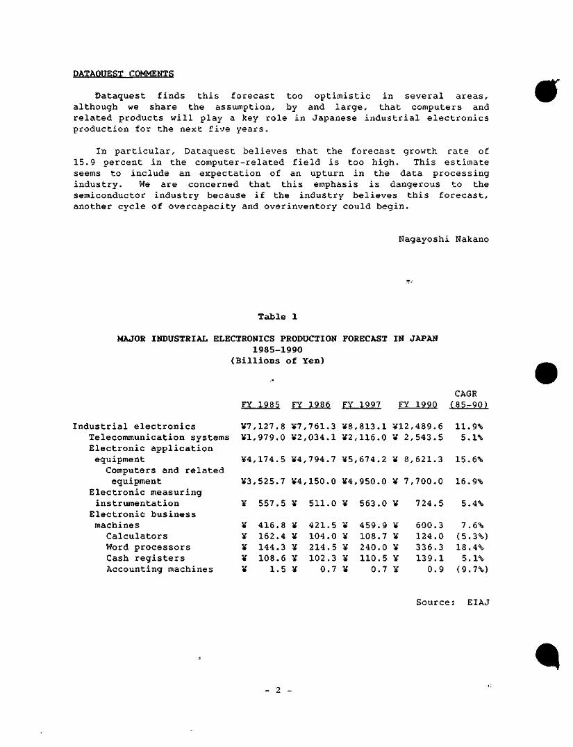
DATAOUEST COMMENTS
Dataquest finds this forecast too optimistic in several areas, although we share the assumption, by and large, that computers and related products will play a key role in Japanese industrial electronics production for the next five years.
#
In particular, Dataquest believes that the forecast growth rate of 15.9 percent in the computer-related field is too high. This estimate seems to include an expectation of an upturn in the data processing industry. We are concerned that this emphasis is dangerous to the semiconductor industry because if the industry believes this forecast, another cycle of overcapacity and overinventory could begin.
Nagayoshi Nakano
Table 1
MAJOR INDUSTRIAL ELECTRONICS PRODUCTION FORECAST IN JAPAN 1985-1990
(Billions of Yen)
Industrial electronics Telecommunication systems Electronic application equipment
Computers and related equipment
Electronic measuring instrumentation
Electronic business machines
Calculators Word processors Cash registers Accounting machines
FY 1985 FY 1986 FY 1997 FY 1990 CAGR (85-90)
¥7,127.8 ¥7,761.3 ¥8,813.1 ¥12,489.6 11.9% ¥1,979.0 ¥2,034.1 ¥2,115.0 ¥ 2,543.5 5.1%
¥4,174.5 ¥4,794.7 ¥5,674.2 ¥ 8,621.3 15.6%
¥3,525.7 ¥4,150.0 ¥4,950.0 ¥ 7,700.0 16.9%
5 5 7 . 5 ¥ 5 1 1 . 0 ¥ 5 6 3 . 0 ¥ 7 2 4 . 5 5 . 4 %
¥ ¥ ¥ ¥ ¥
416.8 162.4 144.3 108.6
1.5
¥ ¥ ¥ ¥ ¥
421.5 104.0 214.5 102.3
0.7
¥ ¥ ¥ ¥ ¥
459.9 108.7 240.0 110.5
0.7
¥ ¥ ¥ ¥ ¥
600.3 124.0 336.3 139.1
0.9
Source
7.6% (5.3%) 18.4% 5.1% (9.7%)
: EIAJ
«
- 2
DataQuesl Tlicbun&BraJun: Li Corpora I ion
JAPANESE RESEARCH
NEWSLETTER
JSIS Code: Newsletters 1985-1986, JSIA 1986-53
1986 JAPANESE CAPITAL SPENDING REVISED DOWNWARD: THE GLOOM DEEPENS
SUMMARY
Continued market sluggishness is forcing Japanese semiconductor makers to reduce their capital spending. After peaking at ¥847 billion ($3.6 billion) in 1984, Japanese semiconductor makers' aapital spending declined by 6.6 percent to ¥791 billion ($3.3 billion) in 1985. As shown in Table 1, Dataquest estimates that Japanese capital spending in 1986 will decrease by 50.9 percent in yen to ¥390 billion ($2.3 billion). We believe that there are several reasons for this decrease in spending:
• Sluggish exports due to the U.S.-Japan Semiconductor Agreement, which has established high foreign market values (FMVs) for commodity products
• Sharply reduced profits in 1986 and potential layoffs in 1987
• Excess capacity and declining domestic prices due to growing competition from new entrants
• The yen shock, which has raised production costs by more than 50 percent within the last year
Due to these severe conditions, Dataquest expects Japanese manufacturers to remain cautious in their capital spending for the foreseeable future. However, we observe three areas of increased activity in this otherwise dismal scenario. First, the U.S.-Japan Semiconductor Agreement is accelerating Japanese plans to build wafer fabs in the United States. Second, several companies such as Japan Semiconductor (LSI Logic KK), New Japan Radio, and Sony, have increased their capital spending since 1984. Third, overall R&D spending is increasing in absolute and relative terms.
© 1986 Dataquest Incorporated December—Reproduction Prohibited
The content of this report represents our interpretation and analysis of information generally available to the public or released by responsible individuals in the subject companies, but is not guaranteed as to accuracy or completeness It does not contain material provided to us in confidence by our clients Individual companies reported on and analyzed by DATAQUEST, may be clients of this and/or other DATAQUEST services This information is nol furnished in connection with a sale or offer to sell securities or in connection with the solicitation of an offer to buy securities This firm and its parent and/or their officers, stockholders, or memtjers of their families may from time to lime, have a long or short position in the securities mentioned and may sell or buy such secunties
Taiyo Ginza Building / 7-14-16 Ginza, Chuo-ku / Tokyo 104, Japan / (03) 546-3191 / Telex J32768 1290 Ridder Park Drive / San Jose, CA 95131-2398 / (408) 971-9000 / Telex 171973
TOP MAKERS LOWER 1986 REVENUE FORECASTS
Lowered revenue forecasts are a major reason for the downward revision in Japanese capital spending. As shown in Table 2, the top six Japanese makers have lowered their 1986 revenue forecasts by an overall 8 percent. Hitachi (-12.8 percent), and Oki Electric (-18.2 percent) show the largest percentage declines.
CAPITAL SPENDING AMONG MAJOR VENDORS
Capital spending by the top nine Japanese semiconductor makers has dropped sharply since 1984. As shown in Table 3, their combined spending decreased by 9.4 percent (in yen) in 1985. Earlier this year, these nine companies had planned to lower their 1986 spending by 24.6 percent (in yen). Due to the market softness, they will lower their 1986 spending plans by 53.6 percent in yen (or 33.9 percent in dollars). Table 4 provides their capital spending in dollar values.
The declines in 1986 capital spending vary by company. Fujitsu (-58.3 percent), Hitachi (-65.2 percent), Matsushita (-69.0 percent), and NEC (-55.3 percent) show the greatest declines, while Mitsubishi (-48.4 percent), Toshiba (-47.2 percent), Sanyo (-34.0 percent). Sharp (-36.1 percent), and Oki Electric (-42.3 percent) plan slightly smaller decreases.
In absolute terms, Toshiba has the highest spending plan (¥65 billion/$389 million), followed closely by NEC (¥55 iDillion $329 million). Toshiba is focusing its investments on its Oita, Himeji, and Kita-Kyushu plants. Recently, Toshiba announced a 50/50 manufacturing joint venture with Motorola in Japan. In Roseville, California, NEC is boosting DRAM production to avoid high FMVs.
NEW MANUFACTURING PLANT ACTIVITIES
Despite the downturn, Japanese semiconductor makers are still adding new production capacity for 256K/lMb DRAMs, ASICs, and MPUs. Their 1986 spending plans are large enough to finance at least one new plant each. Table 5 lists plant expansions, product changes, shutdowns, and delays recently announced by Japanese makers.
Given the U.S.-Japan Semiconductor Agreement, we believe that there is a strong possibility that Japanese companies will add new plant capacity overseas either through direct investment or mutual fab agreements with U.S. and European companies. The Fujitsu/Fairchild and Toshiba/Motorola joint ventures are harbingers of this trend toward fab capacity consolidation. Table 6 summarizes the current plant expansion activities of major Japanese semiconductor makers in the United States and Europe.
- 2 -
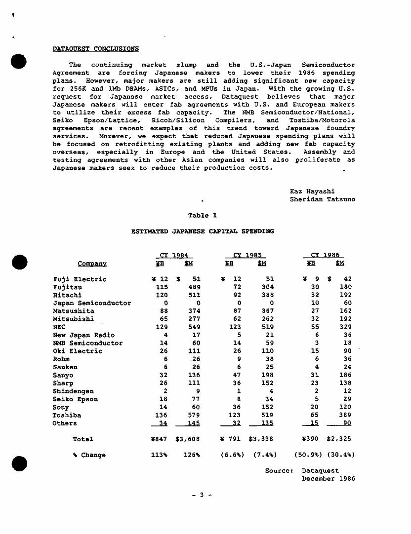
DATAQUEST CONCLUSIONS
The continuing market slump and the U.S.-Japan Semiconductor Agreement are forcing Japanese makers to lower their 1986 spending plans. However, major makers are still adding significant new capacity for 256K and 1Mb DRAMs, ASICs, and MPUs in Japan. With the growing U.S. reguesti for Japanese market access, Dataquest believes that:, major Japanese makers will enter fab agreements with U.S. and European makers to utilize their excess fab capacity. The NMB Semiconductor/National, Seiko Epson/Lattice, Ricoh/Silicon Compilers, and Toshiba/Motorola agreements are recent examples of this trend toward Japanese foundry services. Morever, we expect that reduced Japanese spending plans will be focused on retrofitting existing plants and adding new fab capacity overseas, especially in Europe and the United States. Assembly and testing agreements with other Asian companies will also proliferate as Japanese makers seek to reduce their production costs.
Kaz Hayashi Sheridan Tatsuno
Table 1
ESTIMATED JAPANESE CAPITAL SPENDING
Company
Fuji Electric Fujitsu Hitachi Japan Semiconductor Matsushita Mitsubishi NEC New Japan Radio NMB Semiconductor Oki Electric Rohm Sanken Sanyo Sharp Shindengen Seiko Epson Sony Toshiba Others
CY ¥B
¥ 12 115 120 0 88 65 129 4 14 26 6 6
32 26 2 18 14 136 34
1984 M
$ 51 489 511 0
374 277 549 17 60 111 26 26 136 111 9
77 60 579 145
CY ¥B
¥ 12 72 92 0 87 62 123 5 14 26 9 6
47 36 1 8 36 123 32
1985 M
51 304 388 0
367 262 519 21 59 110 38 25 198 152 4 34 152 519 135
CY MB
¥ 9 30 32 10 27 32 55 6 3 15 6 4 31 23 2 5 20 65 15
1986 M
$ 42 180 192 60 162 192 329 36 18 90 36 24 186 138 12 29 120 389 90
Total
% Change
¥847 $3,608
113% 126%
¥ 791 $3,338
(6.6%) (7.4%)
¥390 $2,325
(50.9%) (30.4%)
Source: Dataquest December 1986
- 3
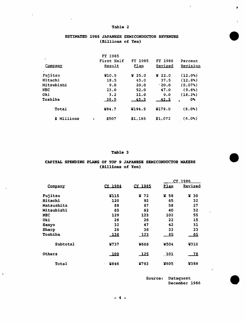
Table 2
ESTIMATED 1986 JAPANESE SEMICONDUCTOR REVENUES (Billions of Yen)
Company
Fujitsu Hitachi Mitsubishi NEC Oki Toshiba
FY 1985 First Half Result
FY 1985 Plan
FY 1985 Revised
Percent Revision
¥10.5 18.5 9.0
23.0 3.2
20.5
¥ 25.0 43.0 20.0 52.0 11.0 43.5
¥ 22.0 37.5 • 20.O 47.0 9.0
43.5
(12.0%) (12.8%) (0.07%) (9.6%)
(18.2%) 0%
Total
$ Millions
¥84.7
$507
¥194.5
$1,165
¥179.0
$1,072
(8.0%)
(8.0%)
Table 3
CAPITAL SPENDING PLANS OF TOP 9 JAPANESE SEMICONDUCTOR MAKERS (Billions of Yen)
Company
Fujitsu Hitachi Matsushita Mitsubishi NEC Oki Sanyo Sharp Toshiba
Subtotal
Others
CY 1984
¥115 120 88 65
129 26 32 26
136
¥737
109
CY 1985
¥ 72 92 87 62
123 26 47 36
123
¥668
125
rv Plan
¥ 58 65 58 40 102 22 42 32 85
¥504
101
IQRfi
Revised
¥ 30 32 27 32 55 15 31 23 65
¥310
78
Total ¥846 ¥793 ¥605 ¥388
Source! Dataquest December 1986
4 -
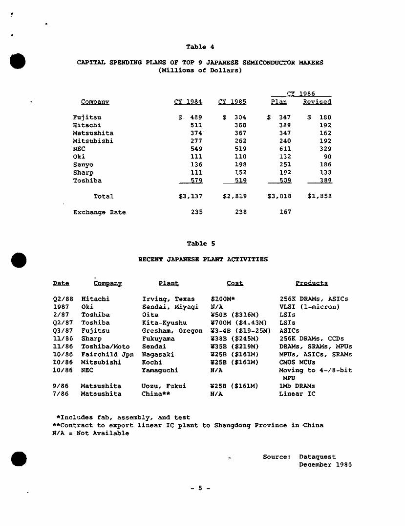
Table 4
CAPITAL SPENDING PLANS OF TOP 9 JAPANESE SEMICONDUCTOR MAKERS (Millions of Dollars)
Company
Fujitsu Hitachi Matsushita Mitsubishi NEC Oki Sanyo Sharp Toshiba
Total
Exchange Rate
CY 1984
$ 489 511 374 277 549 111 136 111 579
$3,137
235
CY
$
$2
1985
304 388 367 262 519 110 198 152 519
,819
238
CY Plan
$
$3
347 389 347 240 611 132 251 192 509
,018
167
1986 Revised
$
$1
180 192 162 192 329 90 186 138 389
,858
Table 5
RECENT JAPANESE PLANT ACTIVITIES
Date Company Plant Cost Products
Q2/88 1987 2/87 Q2/87 Q3/87 11/86 11/86 10/86 10/86 10/86
9/86 7/86
Hitachi Oki Toshiba Toshiba Fujitsu Sharp Toshiba/Moto Fairchild Jpn Mitsubishi NEC
Matsushita Matsushita
Irving, Texas Sendai, Miyagi Oita Kita-Kyushu Gresham, Oregon Fukuyama Sendai Nagasaki Kochi Yamaguchi
Uozu, Fukui China**
$100M* N/A ¥503 ($316M) ¥700M ($4.43M) ¥3-4B ($19-25M) ¥38B ($245M) ¥353 ($219M) ¥253 ($161M) ¥253 ($161M) N/A
¥253 ($161M) N/A
256K DRAMS, ASICs VLSI (1-micron) LSIs LSIs ASICs 256K DRAMS, CCDs DRAMS, SRAMs, MPUs MPUs, ASICs, SRAMs CMOS MCUs Moving to 4-/8-bit MPU 1Mb DRAMS Linear IC
•Includes fab, assembly, and test **Contract to export linear IC plant to Shangdong Province in -China N/A = Not Available
Source: Dataquest December 1986
- 5 -
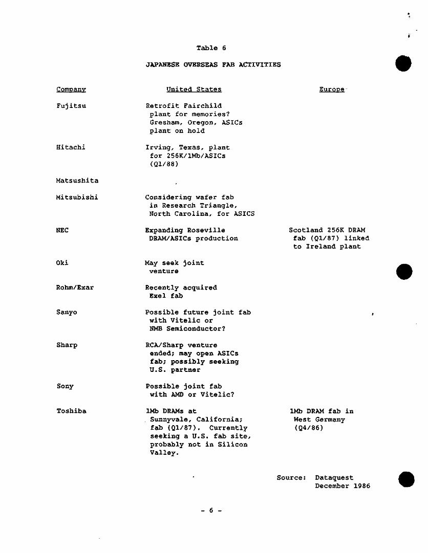
Table 6
JAPANESE OVERSEAS FAB ACTIVITIES
Company
Fujitsu
Hitachi
United States
Retrofit Fairchild plant for memories? Gresham, Oregon, ASICs plant on hold
Irving, Texas, plant for 256K/lMb/ASICs (Ql/88)
Europe -
Matsushita
Mitsubishi Considering wafer fab in Research Triangle, North Carolina, for ASICS
NEC
Oki
Expanding Roseville DRAM/ASICs production
May seek joint venture
Scotland 256K DRAM fab (Ql/87) linked to Ireland plant
Rohm/Exar Recently acquired Exel fab
Sanyo Possible future joint fab with Vitelic or NMB Semiconductor?
Sharp
Sony
RCA/Sharp venture ended; may open ASICs fab; possibly seeking U.S. partner
Possible joint fab with AMD or Vitelic?
Toshiba 1Mb DRAMs at Sunnyvale, California; fab (Ql/87). Currently seeking a U.S. fab site, probably not in Silicon Valley.
1Mb DRAM fab in West Germany (Q4/86)
Source: Dataquest December 1986
- 6 -
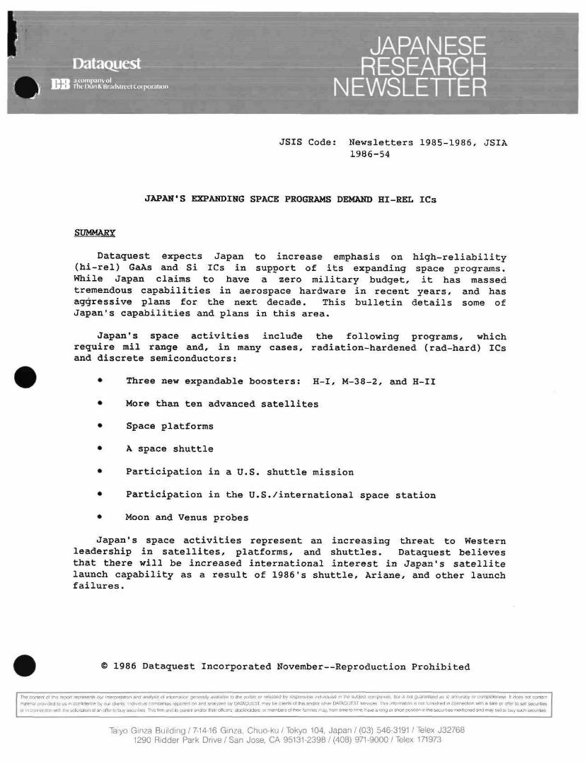
DataQuest ^tompanvol Tho Dun & Bmdsi (nci (. orporadon
JAPANESE RESEARCH
NEWSLETTER
JSIS Code: Newsletters 1985-1986, JSIA 1986-54
JAPAN'S EXPANDING SPACE PROGRAMS DEMAND HI-REL ICs
SUMMARY
Dataquest expects Japan to increase emphasis on high-reliability (hi-rel) GaAs and Si ICs in support of its expanding space programs. While Japan claims to have a zero military budget, it has massed tremendous capabilities in aerospace hardware in recent years, and has aggressive plans for the next decade. This bulletin details some of Japan's capabilities and plans in this area.
requ and
Japan's space activities include the following programs, which re mil range and, in many cases, radiation-hardened (rad-hard) ICs
discrete semiconductors:
Three new expandable boosters: H-I, M-38-2, and H-II
More than ten advanced satellites
Space platforms
A space shuttle
Participation in a U.S. shuttle mission
Participation in the U.S./international space station
Moon and Venus probes
Japan's space activities represent an increasing threat to Western leadership in satellites, platforms, and shuttles. Dataquest believes that there will be increased international interest in Japan's satellite launch capability as a result of 1986's shuttle, Ariane, and other launch failures.
© 1986 Dataquest Incorporated November—Reproduction Prohibited
The content of this report represents our interpretation and analysis of informalion generally available to the public or released by responsible individuals in the subject companies, but is not guaranteed as to accuracy or completeness It does not contain material provided to us in confidence by our clients Individual companies reported on and analyzed by DATAQUEST may be clients of this and/or other DATAQUEST services This information is nol furnished in connection with a sale or offer to sell securities or in connection with the solicitation ot an offer to buy securities This firm and its parent and/or their officers, stockholders, or members of their families may, from lime to time, have a long or shon position in the secunlies mentioned and may sell or buy such securities
Taiyo Ginza Building / 7-14-16 Ginza, Chuo-ku / Tokyo 104, Japan / (03) 546-3191 / Telex J32768 1290 Ridder Park Drive / San Jose, CA 95131-2398 / (408) 971-9000 / Telex 171973
DISCUSSION AND ANALYSIS
Japan has two space agencies: NASDA (National Space Development Agency) and ISAS (Institute of Space and Astronautical Science). These agencies have been responsible for launching about one satellite per year since 1970. MITI (Ministry of International Trade and Industry) serves to create competitive pressures by funding specific payloads.
Japan's space agencies are developing more than 10 satellites and space probes, many designed for geosynchronous orbit (approximately 22,000 miles altitude). These satellites require state-of-the-art GaAs and Si ICs to accomplish the intended functions within launch payload constraints. In addition, rad-hard requirements are expected to impact the IC designs.
Thirteen Japanese companies are studying the MITI/ISAS platform concept for launch by the U.S. shuttle and Japan's H-II booster (developed by Mitsubishi). The H-II booster will support manned launches by 1995. A summary of Japan's spacecraft including launch dates, type of payload and other pertinent data is given in Table 1. These include four communications satellites and two meteorological satellites designed for geosynchronous orbit.
DATAOUEST CONCLUSIONS
Japan is developing a demand for low volumes of domestically produced hi-rel, rad-hard ICs. To achieve better economies of scale, the next logical step is to take these ICs to the international marketplace. Western suppliers of mil-range ICs may experience increased market pressure as a result of Japan's space efforts.
Japan's investment in its space efforts is resulting in far greater capacities in hi-rel semiconductors, satellite systems, and launch hardware than required to support the programs listed in Table 1. In view of recent Western launch failures, we believe that Japan will likely experience increasing difficulty in attempting to keep a low profile regarding its space programs.
Gene Miles
- 2
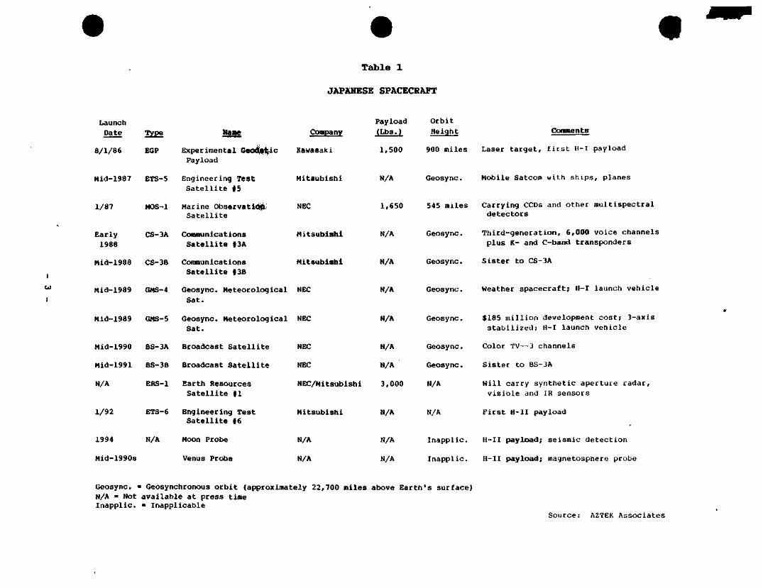
Table 1
JAPANESE SPACECRAFT
I
OJ
I
Launch Date Type
8/1/86 EGP
Mid-1987 ETS-5
1/87 MOS-1
Early CS-3A 1988
Mid-1988 CS-3B
Mid-1989 GMS-4
Mid-1989 GMS-5
Mid-1990 BS-3A
Mid-1991 BS-3fl
N/A ERS-1
1/92 ETS-6
1994 N/A
Mid-1990s
Hame
Experimental Geodietic Pay load
Engineering Test Satellite 15
Marine Obaervatioit Satellite
Communications Satellite t3A
Communications Satellite t3B
Geosync. Meteorological Sat.
Geosync. Meteorological Sat.
Broadcast Satellite
Broadcast Satellite
Earth Resources Satellite «1
Engineering Test Satellite f6
Moon Probe
Venus Probe
Company
Kawasaki
Mitsubishi
NEC
Mitsubishi
Mitsubishi
KEC
Payload (Lbs.)
Orbit Height Comments
NEC
1,500 900 miles Laser target, first H-I payload
N/A
1,650
N/A
N/A
N/A
N/A
Geosync. Mobile Satcom with ships, planes
545 miles Carrying CCDs and ottier multispectral detectors
Geosync. Third-generation, 6,000 voice channels plus K- and C-taand transponders
Geosync. Sister to CS-3A
Geosync. Weather spacecraft; H-I launch vehicle
Geosync.
NEC
NEC
NEC/Mitsubishi
Mitsubishi
N/A
N/A
N/A
N/A
3,000
N/A
N/A
N/A
Geosync
Geosync
N/A
N/A
Inapplii
Inappli'
$185 million development cost! 3-axis stabilized! H-I launch vehicle
Color TV—3 channels
Sister to BS-3A
Will carry synthetic aperture radar, visible and IR sensors
First H-II payload
Inapplic. H-II payload; seismic detection
Inapplic. H-II payload; magnetosphere probe
Geosync. = Geosynchronous orbit (approximately 22,700 miles above Earth's surface) N/A = Not available at press time Inapplic. = Inapplicable
Source: AZTEK Associates
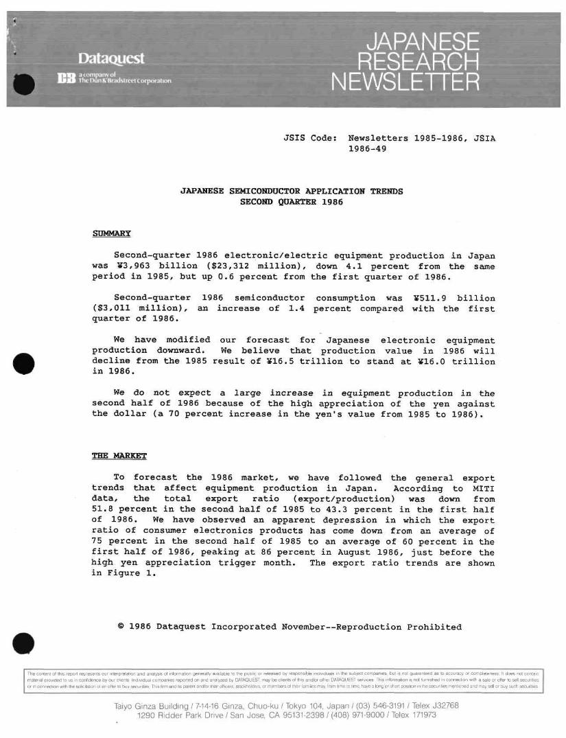
Dataquest acormiarivo) TlK.llunll'arjdMrc£lCcirpn[alioii
JAPANESE RESEARCH
NEWSLETTER
JSIS Code: Newsletters 1985-1986, JSIA 1986-49
JAPANESE SEMICONDUCTOR APPLICATION TRENDS SECOND QUARTER 1986
SUMMARY
Second-quarter 1986 electronic/electric equipment production in Japan was ¥3,963 billion ($23,312 million), down 4.1 percent from the same period in 1985, but up 0.6 percent from the first quarter of 1986.
Second-quarter 1986 semiconductor consumption was ¥511.9 billion ($3,011 million), an increase of 1.4 percent compared with the first quarter of 1986.
We have modified our forecast for Japanese electronic equipment production downward. We believe that production value in 1986 will decline from the 1985 result of ¥16.5 trillion to stand at ¥16.0 trillion in 1986.
We do not expect a large increase in equipment production in the second half of 1986 because of the high appreciation of the yen against the dollar (a 70 percent increase in the yen's value from 1985 to 1986).
THE MARKET
To forecast the 1986 market, we have followed the general export trends that affect equipment production in Japan. According to MITI data, the total export ratio (export/production) was down from 51.8 percent in the second half of 1985 to 43.3 percent in the first half of 1986. We have observed an apparent depression in which the export ratio of consumer electronics products has come down from an average of 7 5 percent in the second half of 1985 to an average of 60 percent in the first half of 1986, peaking at 86 percent in August 1986, just before the high yen appreciation trigger month. The export ratio trends are shown in Figure 1.
© 1986 Dataquest Incorporated November—Reproduction Prohibited
The content of this report represents our Interpretation and analysis ol information generally avaIlable lo the public or released by responsible individuals in the subject companies, but is not guaranteed as to accuracy or completeness It does not contain material provided lo us in conlidence by our clients Individual companies reported on and analyzed by DATAQUEST, may be clients of this and/or other DATAQUEST services This information is not furnished in connection with a sale or offer to sell securities or in conneclion with the solicitation ol an offer to buv securities This firm and its parent and/or their officers, stockholders, or members of their families may, from timelo time, have a long "or short position in the securities mentioned and may sell or buy such securities
Taiyo Ginza Building / 7-14-16 Ginza, Chuo-ku / Tokyo 104, Japan / (03) 546-3191 / Telex J32768 1290 Ridder Park Drive / San Jose, CA 95131-2398 / (408) 971-9000 / Telex 171973
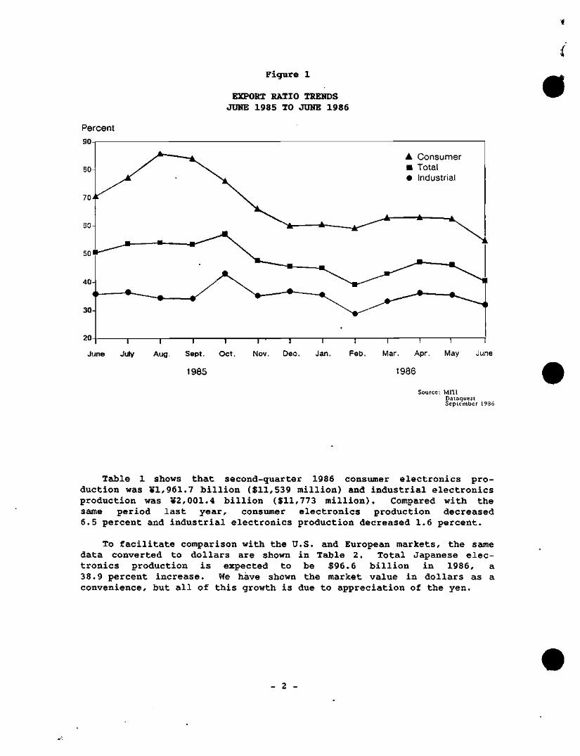
Figure 1
EXPORT RATIO TRENDS JUNE 1985 TO JUNE 1986
#
Percent
90-
20
A Consumer • Total • Industrial
I
June July Aug.
— I
Sept,
1985
~n— Oct. Nov. Dec. Jan.
~!— Feb.
T T"
Mar. Apr.
1986
May June
Source: Mill Dataquesi Seplember 19S6
Table 1 shows that second-quarter 1986 consumer electronics production was ¥1,961.7 billion ($11,539 million) and industrial electronics production was ¥2,001.4 billion ($11,773 million). Compared with the same period last year, consumer electronics p roduct ion decreased 6.5 percent and industrial electronics p roduc t ion decreased 1.6 percent.
To facilitate comparison with the U.S. and European markets, the same data converted to dollars are shown in Table 2. Total Japanese electronics production is expected to be $96.6 billion in 1986, a 38.9 percent increase. We have shown the market value in dollars as a convenience, but all of this growth is due to appreciation of the yen.
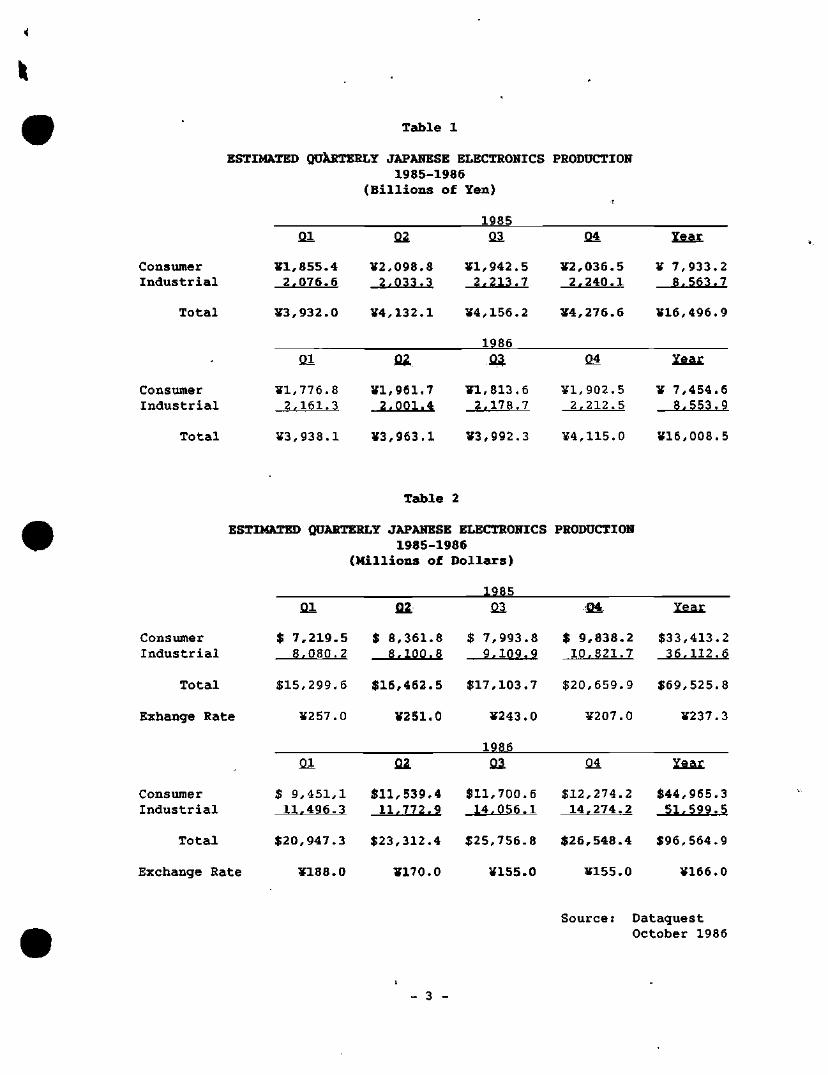
^
Table 1
ESTIMATED QUARTERLY JAPANESE ELECTRONICS PRODUCTION 1985-1986
(Billions of Yen)
1985
Consumer Industrial
Total
Consumer Industrial
Total
21
¥1,855.4 2,076.6
¥3,932.0
01
¥1,776.8 2,161.3
¥3,938.1
Ql
¥2,098.8 2,033.3
¥4,13 2.1
01
¥1,942.5 2,213.7
¥4,156.2
1986
04
¥2,036.5 2,240.1
¥4,276.6
oa ¥1,961.7 2.001.4
¥3,963.1
G3.
¥1,813,6 2,178.7
¥3,992.3
24
¥1,902.5 2.212.5
¥4,115.0
Year
¥ 7,933.2 8.563.7
¥16,496.9
Year
¥ 7,454.6 8.553.9
¥16,008.5
Table 2
ESTIMATED QUARTERLY JAPANESE ELECTRONICS PRODUCTION 1985-1986
(Millions of Dollars)
1985
Consumer Industrial
21
$ 7,219.5 8.080.2
$ 8,361.8 8,100.6
01
$ 7,993.8 9,109.9
$ 9,838,2 10.821.7
Year
$33, 36,
, 413 . .112,
,2 ,6
T o t a l
Exhange Rate
Consumer Industrial
$15,299.6
¥257,0
21
$16,462.5
¥251.0
$17,103.7
¥243.0
1986
$20,659.9
¥207.0
22 01 24
$ 9,451,1 $11,539.4 $11,700.6 $12,274.2 11.496.3 11.772.9 14.056.1 14,274,2
$69,525.8
¥237.3
Year
$44,965,3 51.599.5
Total
Exchange Rate
$20,947.3 $23,312.4 $25,756.8 $26,548,4 $96,564.9
¥188.0 ¥170.0 ¥155.0 ¥155.0 ¥166.0
Source: Dataquest October 1986
- 3
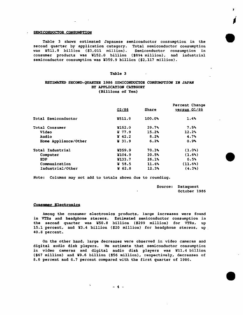
SEMICONPUCTOR CONSUMPTION
Table 3 shows estimated Japanese semiconductor consumption in the second quarter by application category. Total semiconductor consumption was ¥511.9 billion ($3,011 million). Semiconductor consiunption in consumer products was ¥152.0 billion ($894 million), and industrial semiconductor consumption was ¥359.9 billion ($2,117 million).
Table 3
ESTIMATED SECOND-QUARTER 1986 SEMICONDtJCTOS CONSUMPTION IN JAPAN BY APPLICATION CATEGORY
(Billions of Yen)
/
Total Semiconductor
Total Consumer Video Audio Home Appliance/Other
Total Industrial Computer EDP Communication Industrial/Other
02/86
¥511.9
¥152.0 ¥77.9 ¥ 42.2 ¥ 31.9
¥359.9 ¥104.9 ¥133.7 ¥58,5 ¥ 62.8
Share
100.0%
29.7"% 15.2% 8.2% 6.2%
70,3% 20,5% 26,1% 11.4% 12.3%
Percent Change versus 01/86
1.4%
7.5% 12.2% 4.7% 0,9%
(1.0%) (1.6%) 6.5%
(11.6%) (4.3%)
Note: Columns may not add to totals shown due to rounding.
Source: Dataquest October 1986
Consumer Electronics
Among the consumer electronics products, large increases were found in VTRs and headphone stereos. Estimated semiconductor consumption in the second quarter was ¥50,8 billion ($299 million) for VTRs, up 15.1 percent, and ¥3.4 billion ($20 million) for headphone stereos, up 40.8 percent.
On the other hand, large decreases were observed in video cameras and digital audio disk players. We estimate that semiconductor consumption in video cameras and digital audio disk players was ¥11.4 billion ($67 million) and ¥9.6 billion ($56 million), respectively, decreases of 8.6 percent and 6.7 percent compared with the first quarter of 1986.
4 -
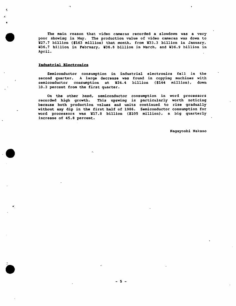
The main reason that video cameras recorded a slowdown was a very poor showing in May. The production value of video cameras was down to ¥27.7 billion ($163 million) that month, from ¥33.3 billion in January, ¥36.7 billion in February, ¥36.8 billion in March, and ¥36.9 billion in April.
Industrial E lectronics
Semiconductor consumption in industrial electronics fell in the second quarter. A large decrease was found in copying machines with semiconductor consumption at ¥24.4 b i l l i o n ($144 million), down 10.3 percent from the first quarter.
On the other hand, semiconductor consumption in word processors recorded high growth. This upswing is particularly worth noticing because bo th production values and units continued to rise gradually without any dip in the first half of 1986. Semiconductor consumption for word processors was ¥17.8 billion ($105 million), a big quarterly increase of 45.8 percent.
Nagayoshi Nakano
Dataquest .1 (tinipanv ol lhi'I^un&T1i:<(lstri;cilorp(tr;iThin
JAPANESE RESEARCH
NEWSLETTER
JSIS Code: Newsletters 1985-1986, JSIA 1986-50
KOREAN SEMICONDUCTOR COOPERATIVE RESEARCH PROJECT
INTRODUCTION
This report is the third in a series to supplement the Korean Semiconductor Industry Analysis, which was published in March 1986.
South Korea's emergence as an internationally competitive semiconductor component supplier introduces both a challenge and threatening situation.
As Korean companies complete the first phase of building their manufacturing lines, they are concerned about how to fill the huge capacity they have established. Current capacity is estimated at approximately 2.5 million wafer starts of 5-inch equivalent per year. Current utilization is estimated at 50 percent, with some companies reporting higher than average usage.
Initially, Korea has followed Japan's strategy, concentrating on the commodity memory products, such as 64K and 256K DRAMs. However, advanced product design know-how and the design engineering resources of the individual companies is limited. Therefore, we believe that production of products beyond 1Mb DRAM will be quite difficult. The Korean government recognized this problem and initiated a dialogue among Korean semiconductor companies as early as the summer of 1985 to form a cooperative effort to produce advanced memory products. This effort began to materialize in the spring of 1986 in the form of a formal cooperative project known as the Korean Semiconductor Cooperative Research Project (also known as the Korean VLSI Project).
THE KOREAN SEMICONDUCTOR COOPERATIVE RESEARCH PROJECT
The Project was formally launched on April 10, 1986, organization was announced immediately, as shown in Figure 1.
and its
• *
1986 Dataquest Incorporated November—Reproduction Prohibited
The content of IhIs report represents cur interprelation and analysis of information generally available to the public or released by responsible indivIduais in the subject companies, but is not guaranteed as to accuracy or completeness It does not contain material provided to us in confidence by our clIents Individual companies reported on and analyzed by DATAQUEST, may be clients of thIs and/or other DATAQUEST services This information Is not furnished in connection with a sale or offer to sell securities Of in connection wIih the solicIlation of an offer to buy securities This lifm and its parent and/or their officers, stIackholders, or members ol theIr families may, from time lo time, have a long or short positIon In the securities mentIoned and may sell or buy such securities
Taiyo Ginza Building / 7-14-16 Ginza, Chuo-ku / Tokyo 104, Japan / (03) 546-3191 / Telex J3276B 1290 Ridder Park Drive / San Jose, CA 95131-2398 / (408) 971-9000 / Telex 171973
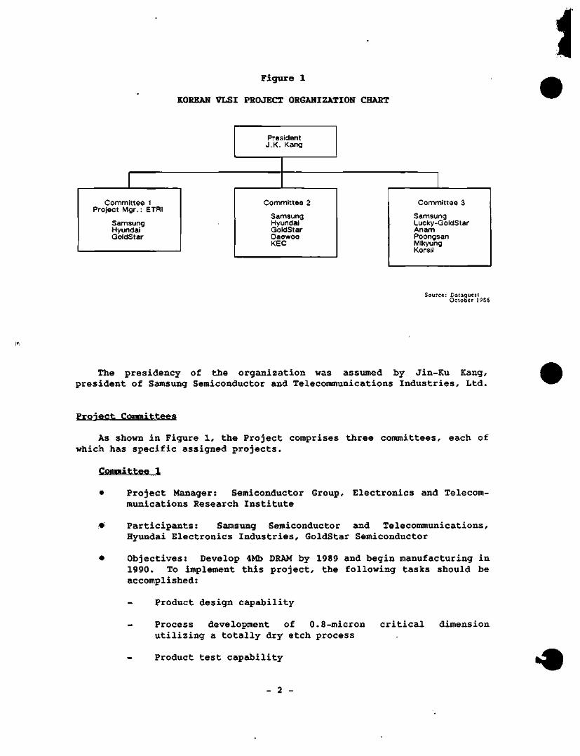
I Figure 1
KOREAN VLSI PROJECT ORGANIZATION CHART
Cominittee 1 Project Mgr.: ETRI
Samsung Hyundai GoldStar
President J.K. Kang
Committee 2
Samsung Hyundai GoldStar Daewoo KEC
Committee 3
Samsung Lucky-GoldStar An am Poongsan MIkyung Korsll
Source: Dataquest October 19S6
The presidency of the organization was assumed by Jin-Ku Kang, president of Samsung Semiconductor and Telecommunications Industries, Ltd.
Project Commit:t:ees
As shown in Figure 1, the Project comprises three committees, each of which has specific assigned projects.
Committee 1
• P r o j e c t Manager: Semiconductor Group, Electronics and Telecommunications Research Institute
Participants: Samsung Semiconductor and Telecommunications, Hyundai Electronics Industries, GoldStar Semiconductor
Objectives: Develop 4Mb DRAM by 1989 and begin manufacturing in 1990. To implement this project, the following tasks should be accomplished:
- Product design capability
- Process development of 0.8-micron critical dimension utilizing a totally dry etch p rocess
- Product test capability «
2 -
Coimnittiee 2
• P r o j e c t Manager: Not a s s i g n e d
• Participants: Samsung Semiconduc to r and T e l e c o m m u n i c a t i o n s , Hyundai Electronics Industries, GoldStar Semiconductor, Daewoo T e l e c o m m u n i c a t i o n s (Semiconductor), Korea E l e c t r o n i c s Co. (KEC)
• Objective: Nonmemory-related IC projects:
Advance consumer IC products by 1989
Establish IC design automation technology, such as simulator, layout so f tware , standard cell library, by 1991
Establish 1-micron ASIC techno logy by 1991
Develop 32-bit and 64-bit microprocesso rs by 1991
Develop industrial ICs, such as smart power devices, by 1989
Develop ISDN ICs by 1991
Coimnititee 3
• P r o j e c t Manager: Not assigned
• Participants: Samsung Group, L u c k y - G o l d S t a r Group, Anam, Poongsan, Mikyung, Korsil
• Objective: Develop support industries
Establish ability to produce very high-purity silicon wafers by 1990
Produce compound semiconductors, GaAs, InP, and others by 1991
Produce chemicals, specialty gases by 1991
Qualify lead-frame material PMC 102 by 1988
Develop and manufacture bonding wire by 1989
Produce certain packaging equipment by 1989
PROJECT FUNDING
The Korean VLSI Project funding is to be shared equally by government and industry. However, the industry portion will be heavily subsidized by government-guaranteed, low interest loans. Table 1 shows the project funding allocated through 1988.
- 3
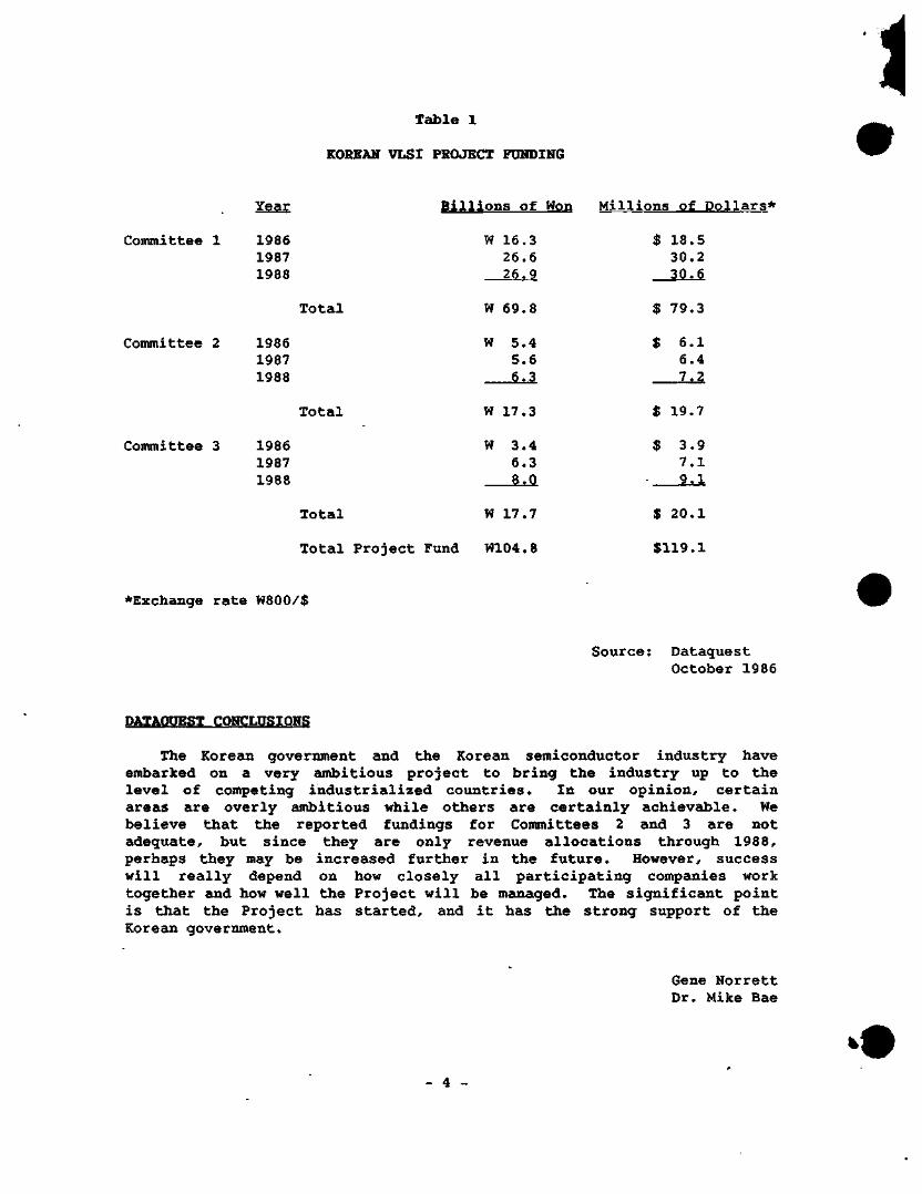
i Table 1
KOREAN VLSI PROJECT FINDING
Committee 1
Commit tee 2
Committee 3
Year
1986 1987 1988
Billions of Won Millions of Dollars*
Total
1986 1987 1988
Total
1986 1987 1988
W 16.3 26.6 2 .9
W 69.8
W
W
w
W
5 . 4 5 . 6
$ f 3
1 7 . 3
3 . 4 6 . 3
9.0
1 7 . 7 Total
Total Project Fund W104.8
$ 1 8 . 5 3 0 . 2 3 0 . 6
$ 79.3
$ 6 . 1 6 .4
L L I
$ 1 9 . 7
$ 3 . 9 7 . 1 9 . 1
$ 2 0 . 1
$ 1 1 9 . 1
^Exchange rate W800/$
Source: Dataquest October 1986
DATAQUEST CONCLUSIONS
The Korean government and the Korean semiconductor industry have embarked on a very ambit ious p r o j e c t to bring the industry up to the level of competing industrialized c o u n t r i e s . In our opinion, certain areas are overly ambit ious while others are certainly achievable. We believe that the r epo r t ed fundings for Committees 2 and 3 are not adequate, but since they are only revenue a l l o c a t i o n s tJirough 1988, perhaps they may be increased further in the future. However, success will really depend on how closely all participating companies work together and how well the Project will be managed. The significant point is that the Project has started, and it has the s t rong support of the Korean government.
Gene Norrett Dr. Mike Bae
Dataquest acumpaiiyo) ThcDunil'nrjcUlrcciCUfpotstiun
JAPANESE RESEARCH
NEWSLETTER
JSIS Code: Newsletters 1985-1986, JSIA 1986-51
SYMPOSIUM HIGHLIGHTS LATEST GaAs IC DEVELOPMENTS
SUMMARY
The 1986 IEEE-sponsored GaAs IC Symposium and associated activities served the emerging GaAs IC industry as an excellent forum for the interchange of R&D and manufacturing concepts and practices. A design workshop preceded the three days of meetings; a manufacturing conference (open only to citizens and permanent residents of the United States of America) followed the symposium. Fifty-five papers (selected from 126 submissions) and four panel sessions covered a broad range of topics: diglCs, MMICs, materials, design, testing, manufacturing, and others. The United States was well represented, giving 41 papers (75 percent). Japan was represented by 9 papers (16 percent), followed by France (3 papers), the United Kingdom (2 papers), and Canada (1 paper). Speakers from West Germany and several other countries were notably absent, although GaAs R&D is progressing in those countries as well. Conference attendance exceeded 830 persons.
Some significant advances in GaAs ICs in 1986 were:
• Development of 4-inch NDF (near-defect-free) GaAs wafers
* Demonstration of 600ps IKxl SRAMs
* ECL-compatible one gigasample/sec. 8-bit DAC with untrimmed nichrome resistors on-chip
• Operation of GaAs MMIC amplifier with 135mW output power at 41 GHz
• Successful multiple-sourclng of GaAs 12x12 multiplier chips
• Development of 88-pin LCC for 8-GHz operation in 50-0hm system
1986 Dataquest Incorporated November—Reproduction Prohibited
The content o( this report represents our interpretation and analysis of information generally availaWe lo ihe public or released by responsible individuals in the subject companies, but is not guaranteed as to accuracy or completeness It does ncA contain material provided to us in confidence by our clients Individual companies reported on and analyzed by DATAQUEST, may be clients of this and/or other DATAQUEST services This information is not furnished in conneciion with a sale or offer to sell securities or in conneclton with the solicilation of an offer to buy securities This firm and its parent and/or Iheir officers, stockholders, or members of their families may, from time to lime, have a long or short position in the securities mentioned and may sell or buy such securities
Taiyo Ginza Building / 7-14-16 Ginza, Chuo-ku / Tokyo 104, Japan / (03) 546-3191 / Telex J32768 1290 Bidder Park Drive / San Jose, CA 95131-2398 / (408) 971-9000 / Telex 171973
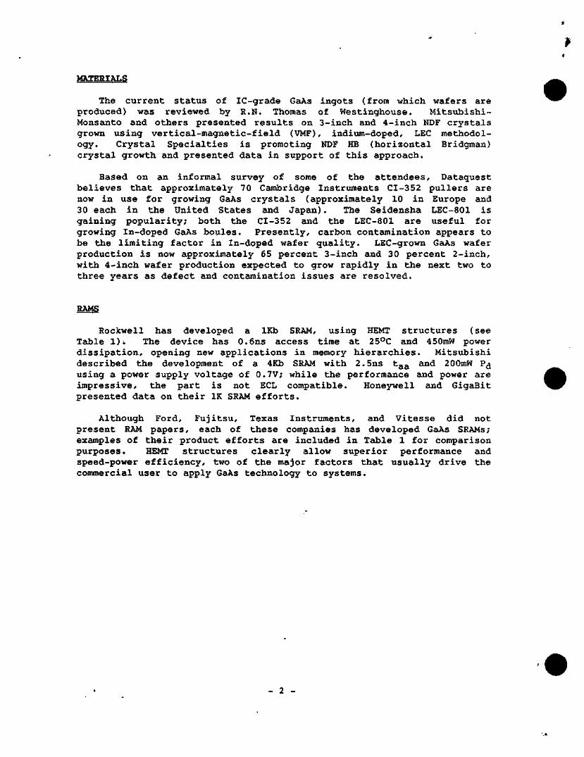
MATERIALS
The current status of IC-grade GaAs ingots (from which wafers are produced) was reviewed by R.N. Thomas of Westinghouse. Mitsubishi-Monsanto and others presented results on 3-inch and 4-inch NDF crystals grown using vertical-magnetic-field (VMF), indium-doped, LEG methodology. Crystal Specialties is promoting NDF HE (horizontal Bridgman) crystal growth and presented data in support of this approach.
Based on an informal survey of some of the attendees, Dataguest believes that approximately 70 Cambridge Instruments CI-352 pullers are now in use for growing GaAs cryst;als (approximately 10 in Europe and 30 each in the United States and Japan). The Seidensha LEC-801 is gaining popularity; both the CI-352 and the LEC-801 are useful for growing In-doped GaAs boules. Presently, carbon contamination appears to be the limiting factor in In-doped wafer quality. LEC-grown GaAs wafer production is now approximately 65 percent 3-inch and 30 percent 2-inch, with 4-inch wafer production expected to grow rapidly in the next two to three years as defect and contamination issues are resolved.
RAMS
Rockwell has developed a 1Kb SRAM, using HEMT structures (see Table 1). The device has 0.6ns access time at 25°C and 450mW power dissipation, opening new applications in memory hierarchies. Mitsubishi described the development of a 4Kb SRAM with 2. 5ns t-g and 200mW Pj using a power supply voltage of 0.7V; while the performance and power are impressive, the part is not ECL compatible. Honeywell and GigaBit presented data on their IK SRAM efforts.
Although Ford, Fujitsu, Texas Instruments, and Vitesse did not present RAM papers, each of these companies has developed GaAs SRAMs; examples of their product efforts are included in Table 1 for comparison purposes. HEMT structures clearly allow superior performance and speed-power efficiency, two of the major factors that usually drive the commercial user to apply GaAs technology to systems.
- 2 -
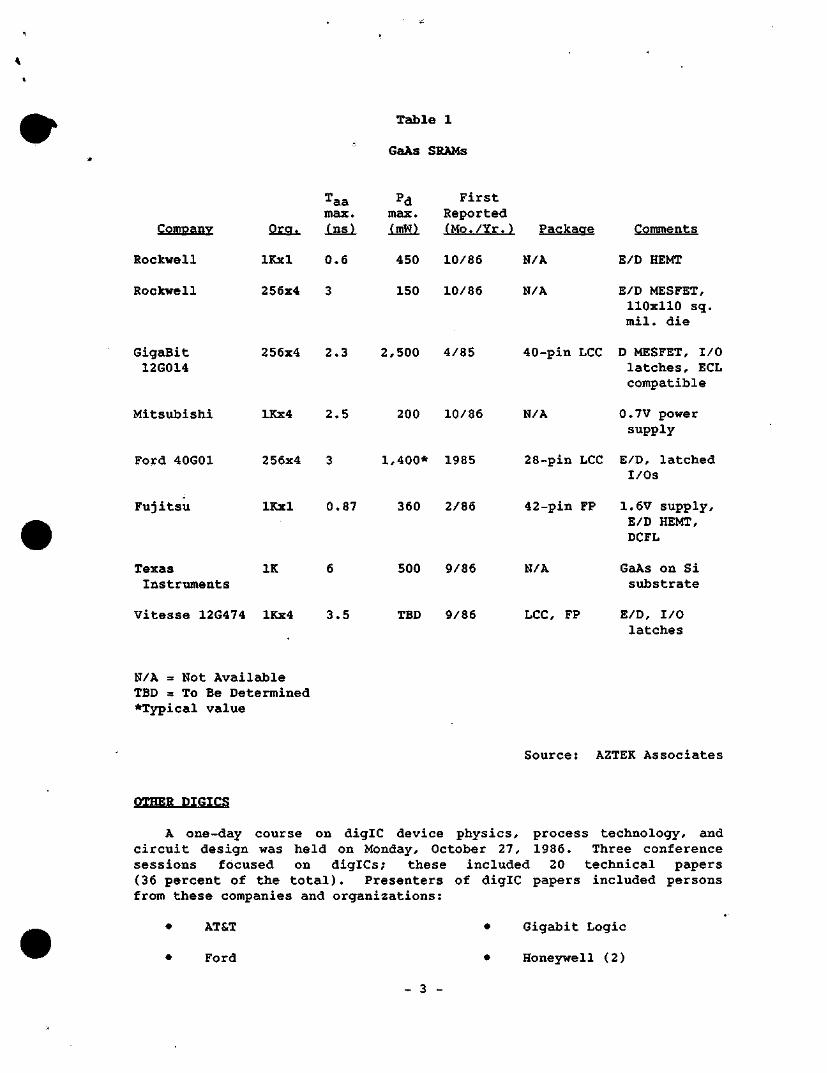
company
Rockwell
Rockwell
GigaBit 12G014
Mitsubishi
Org.
IKxl
256x4
256x4
lKx4
Taa max. (ns)
0.6
3
2.3
2.5
Table
GaAs
Pd max. (mW)
450
150
2,500
200
1
SBAMs
First Reported (Mo./Yr.)
10/86
10/86
4/85
10/86
Package
N/A
N/A
40-pin LCC
N/A
Comments
E/D HEMT
E/D MESFET, 110x110 sq. mil. die
D MESFET, I/O latches, ECL compatible
0.7V power supply
Ford 40G01 256x4 3 1,400* 1985 28-pin LCC E/D, latched I/Os
Fujitsu IKxl 0.87 360 2/86 42-pin FP 1.6V supply, E/D HEMT, DCFL
Texas IK Instruments
500 9/86 N/A GaAs on Si substrate
Vitesse 12G474 lKx4 3.5 TED 9/86 LCC, FP E/D, I/O latches
N/A = No t Available TED = To Be Determined *Typical value
OTHER DIGICS
Source: AZTEK Associates
A one-day course on digIC device physics, process technology, and circuit design was held on Monday, October 27, 1986. Three conference sessions focused on diglCs; these included 20 technical papers (36 percent of the total). Presenters of digIC papers included persons from these companies and organizations:
AT&T
Ford
Gigabit Logic
Honeywell (2)
- 3 -
IBM 4 NTT (3)
ITT * Oki
Matsushita • Plessey
Mayo Foundation * Rockwell (4)
McDonnell Douglas • TriQuint
Mitsubishi • TRW
Multiplexer/demultiplexer chips from Matsushita, NTT, Oki, and Rockwell/TriQuint, geared toward fiber-optic applications in the 1- to 3-GHz range, attracted much interest. A Honeywell/Mayo Foundation team has developed and multisourced a 6,000-gate array based on SDFL Structures and has tested it to 160°C operating temperature. This chip contrasts with the largest ECL gate array to date, which has 8,000 gates and maximum operating temperature of 125°C. The 6,000-gate GaAs array has 176 I/O leads plus 40 power/ground leads, and it has been used to implement a single-chip 12x12 multiplier.
HBT (heterojunction bipolar transistor) structures offer very high performance potential in digital systems because of the very high cutoff frequency of HBTs (f . to 456 GHz). Rockwell reported the first uncom-pensated-CML MSI circuits in HBT, including a 3-GHz 8-bit shift register. TRW (Internal R&D) and Plessey (ESPRIT Program project) also reported HBT results. Although p rogress has been made, the integration level of HBT is not yet sufficient to offer a speed advantage compared to s i l i c o n ECL LSI. Also , temperature compensation is needed to enhance usefulness of HBT ICs.
MMICs
Texas Instruments reported MMIC power amplifiers with output power of 200mW at 34 GHz and 135mW at 41 GHz. Hughes described a 1.3W output 7-15.5 GHz MMIC amplifier. ITT, Pacific Monolithics, LEP (Philips), and Raytheon authors described their work in other special-purpose MMICs. These chips allow users to further miniaturize communications and other equipment.
Fabrication
Ford Microelectronics detailed a self-aligned, low temperature E/D process that is employed in Ford's 561-cell 4-input NOR array, IK SRAM, and other LSI chips. Ford's exhibit included a demonstration of a multiplier implemented with the 561-cell array chip. Matsushita described an all-implant MMIC process. Hughes has developed an E/D process using pure tungsten gates. Hewlett-Packard presented a method for improved control of threshold voltage, heretofore a significant limiting factor in GaAs IC development. Together, the papers represent a maturing of GaAs IC fabrication technology.
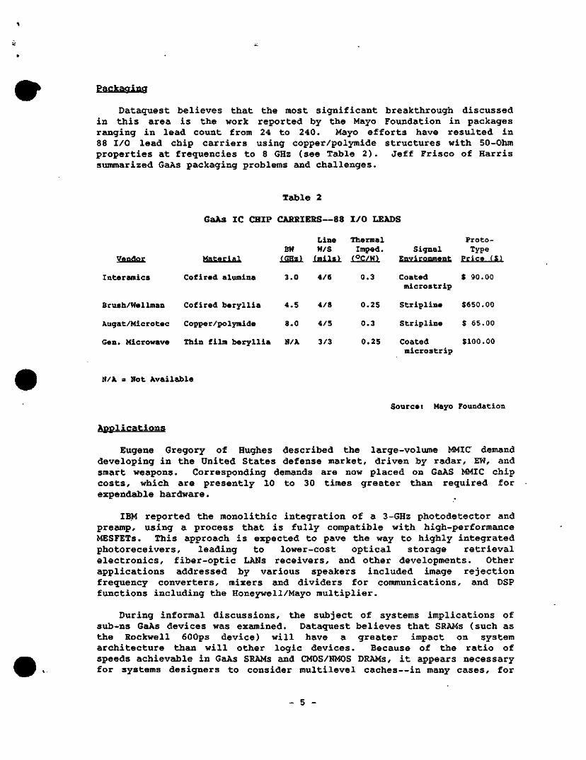
Packacfinq
Dataguest believes that the most significant breakthrough discussed in this area is the work reported by the Mayo Foundation in packages ranging in lead count from 24 to 240. Mayo efforts have resulted in 88 I/O lead chip carriers using c o p p e r / p o l y m i d e structures with 50-Ohm properties at frequencies to 8 GHz (see Table 2). Jeff F r i s co of Harris summarized GaAs packaging p r o b l e m s and challenges.
Table 2
GaAs IC CHIP CARRIERS—88 I/O LEADS
Interamics
Brush/Wellman
Mater4*l
Cofired alumina
Cofired beryllia
Copper/polymide
Thin film beryllia
BH (5H?)
3.0
4.5
8.0
N/A
Line W/S fmils)
4/6
4/8
4/5
3/3
Thermal Imped. CC/W)
0.3
0.25
0.3
0.25
Signal Environment
Coated microstrip
Stripline
Stripline
Coated microstrip
Proto-Type
Price ($)
$ 90.00
$650.00
$ 65.00
$100.00
N/A 3 Hot Available
Applications
Source: Mayo Foundation
Eugene Gregory of Hughes described the large-volume MMIC demand developing in the United States defense market, driven by radar, EW, and smart weapons. Corresponding demands are now placed on GaAS MMIC chip c o s t s , which are presently 10 t o 30 times greater than required f o r expendable hardware.
IBM reported the mono l i th ic i n t e g r a t i o n of a 3-GHz pho tode tec to r and preamp, using a p r o c e s s that is fully compatible with high-performance MESFETs. This a p p r o a c h is expected to pave the way t o highly integrated p h o t o r e c e i v e r s , leading t o lower-cost optical storage retrieval electronics, fiber-optic LANs receivers, and other developments. Other applications addressed by various speakers included image rejection frequency converters, mixers and dividers for communications, and DSP functions including the Honeywell/Mayo multiplier.
During informal discussions, the subject of systems implications of sub-ns GaAs devices was examined. Dataquest believes that SRAMs (such as the Rockwell 600ps device) will have a greater impact on system architecture than will other logic devices. Because of the ratio of speeds achievable in GaAs SRAMs and CMOS/NMOS DRAMs, it appears necessary for systems designers to consider multilevel caches—in many cases, for
5 -
the first time. In a multilevel cache approach, the first-level GaAs cache RAM will probably be most efficient if placed on the processor package. The second- level cache techno logy is open to question; 5 to 10ns ECL or 15ns CMOS SRAM may be more appropriate than GaAs due to the number of chips and corresponding interconnect impedances involved. Locat ion of second-level cache is critically dependent on relative timing of loaded devices as well as other factors.
GaAs INPnSTRY TRENDS
Many attendees are involved in bringing GaAs technology to bear on some of the electronics industry's most challenging problems. There is a growing concern that U.S. and European users of ICs are allowing their Japanese competitors to beat them to market with products that take advantage of this critical technology. Increasingly, the problem is no longer one of availability but one of acceptance; currently, products exist and capacity goes unused. The military arena, despite strong budget pressures, is pressing forward to take advantage of the unique properties of GaAs. However, if a broad range of customers' price demands are to be met, a strong commercial applications base must develop to provide adequate economies of scale, not unlike the "chicken and egg" scenario in the silicon world in 1969.
DATAOUEST CONCLUSIONS
GaAs ICs are here to stay. Suppliers are making great strides toward production of functions suitable for tommorrow's high-performance systems. Dataquest believes that the growing number of systems houses presently making judicious use of this techno logy will help create their own economic recovery despite overall market conditions. It's November 1986; do you know what your compet i to rs are doing with GaAs technology?
Gene Miles
Dataquest 3 tutitpany ul TitcDun&'BraditrceICorpornliDn
JAPANESE RESEARCH
NEWSLETTER
JSIS Code: Newsletters 1985-1986, JSIA 1986-48
U.S.-JAPAN SEMICONDUCTOR TRADE UPDATE: SECOND QUARTER 1986
TRADE STATISTICS
Bilateral U.S.-Japan semiconductor trade continued an upward trend in the s econd quarter of 1986, with imports of U.S. semiconductors into Japan up 17.4 percent and exports of Japanese semiconductors to the United States up 2.5 percent, according to Japanese Ministry of Finance (MOF) figures.
Although there is no doubt that the rising yen was partially r e s p o n s i b l e for the increase in U.S. imports into Japan, import growth actually exceeded the growth in yen value by 6.8 percent. The yen grew 10.6 percent from the first quarter to the second quarter of 1986 (from $0.005319 per «1 to $0.005882 per ¥1), while U.S. imports into Japan grew 17.4 percent.
Japanese exports to the United States grew only 2.5 percent, considerably slower than the U.S. semiconductor market, which was up 14.4 percent. However, several Japanese firms announced plans early in the second quarter to shift distribution and production plans, in order to evade the dumping penalties on DRAMs and EPROMs that were imposed in late March 1986. A shift in assembly sites to Europe or other "third countries" for chips aimed at the U.S. market, combined with financial pressures of the high yen and dumping penalties, could account for the small second-quarter increase in exports.
MOS memory exports from Japan to the United States remained low as a percentage of total exports, accounting for 41 percent, down from 43 percent in first quarter 1986.
Bipolar digital IC imports from the United States to Japan, as a percentage of total imports, appeared to be up in both the first and second quarters of 1986. This category accounted for 33 percent of total imports in the second quarter, while it averaged only 18 percent of total imports during 1985.
1986 Dataquest Incorporated November—Reproduction Prohibited
The conleni ot this report represents our interpretation and analysis of information generally available to the public or released by responsible individuals in the subject companies, but is not guaranteed as to accuracy or completeness It does not contain material provided to us in confidence by our clients Individual companies reported on and analyzed by DATAQUEST, may be clients of this and/or other DATAQUEST services This information is not furnished in connection with a sale or offer to sell securities or in conneclion wilh the soiicitation of an offer to buy securities This firm and its parent and/or their officers, stockholders, or members of their families may, from time to lime, have a long or short position in the securities mentioned and may sell or buy such securities
Taiyo Ginza Building / 7-14-16 Ginza, Chuo-ku / Tokyo 104, Japan / (03) 546-3191 / Telex J32768 1290 Ridder Park Drive / San Jose,- CA 95131-2398 / (408) 971-9000 / Telex 171973
Table 1 shows quarterly exports of Japanese semiconductors to the United States. Imports of U.S. semiconductors into Japan are shown in Table 2. In both tables,- total integrated circuit and discrete plus optoelectronic figures are from MOF; the integrated circuit split by product line is estimated from U.S. Departunent of Commerce (DOC) figures.
The United States continued to maintain a positive trade balance in bipolar digital logic and linear ICs, as shown in Table 3; however, the overall trade balance was negative $103 million in the second quarter of 1986. It must be pointed out that this represents a decrease from the first quarter in the U.S. semiconductor trade deficit with Japan. The total U.S.-Japan semiconductor trade picture is illustrated in Figure 1.
Tables 4 and 5 show quarter-to-quarter and year-to-year growth in semiconductor trade between the United States and Japan from the first quarter of 1984 through the second quarter of 1986.
DATAOUEST ANALYSIS
We are beginning to see major changes in the way Japanese companies conduct business in the United States. We believe that these changes are due t o :
# The semiconductor "trade war" between Japan and the United States
•4 The preliminary dumping penalties levied beginning in the second quarter of 1986
# The upward spiral of the yen, which finally appears to be at rest
# The final signing of the U.S.-Japan Semiconductor Trade Arrangement, which requires Japanese companies to buy more U.S. chips, and a l s o imposes "foreign market values" (FMVs), assigned on a company-by-company basis by the U.S. DOC, on Japanese-manufactured chips sold in foreign markets
Japanese companies are shifting p roduc t ion of end equipment to Asia to cut costs. Many Japanese companies are studying U.S. companies to determine which ones may be ripe for takeovers, as a way of establishing production bases in the United States, as well as acquiring U.S. technology. The purchase of 80 percent of Fairchild by Fujitsu is a case in point. If Fujitsu can shift production of EPROMs and 256K and above DRAMs to Fairchild, it can avoid FMVs and also save itself the expense of building a factory at its Gresham, Oregon, site.
We are now collecting data for our preliminary 1986 market share estimates. Early next year we will publish the annual results of actual sales in Japan by U.S. companies and in the United States by Japanese companies.
Patricia S. Cox
2 -
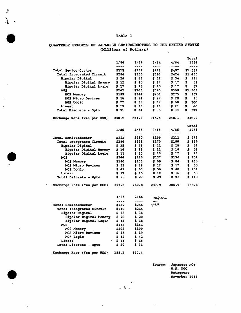
Table 1
QUARTERLY EXPORTS OF JAPANESE SEMICONDUCTORS TO THE UNITED STATES (Millions of D o l l a r s )
Total Semiconductor Total Integrated Circuit
Bipolar Digital Bipolar Digital Memory Bipolar Digital Logic
MOS MOS Memory MOS Micro Devices MOS Logic
Linear Total Discrete •» Opto
1/84
$315 $284 $ 29 $ 12 $ 17 $242 $199 $ 16 $ 27 $ 13 $ 31
2/84
$389 $355 $ 33 $ 15 $ 18 $306 $244 $ 24 $ 38 $ 16 $ 34
3/84
$428 $393 $ 32 $ 17 $ 15 $345 $251 $ 27 $ 67 $ 16 $ 35
4/84
$457 $424 $ 34 $ 17 $ 17 $369 $273 $ 28 $ 68 $ 21 $ 33
Total 1984
$1,589 $1,456 $ 128 $ 61 $ 67 $1,262 $ 967 $ 95 $ 200 $ 66 $ 133
Exchange Hate (Yen per US$) 230.5 231.9 246 .6 2 4 8 . 1 240 .2
Total Semiconductor Total Integrated Circuit
Bipolar Digital Bipolar Digital Memory Bipolar Digital Logic
MOS MOS Memory MOS Micro Devices MOS Logic
Linear Total Discrete •«• Opto
1/85
$311 $286 $ 25 $ 14 $ 11 $244 $180 $ 22 $ 42 $ 17 $ 25
2/85
$250 $223 $ 23 $ 13 $ 10 $185 $103 $ 19 $ 63 $ 15 $ 27
3/85
$199 $170 $ 21 $ 11 $ 10 $137 $ 69 $ 12 $ 56 $ 12 $ 29
4/85
$212 $180 $ 28 $ 16 $ 12 $136 $ 84 $ 12 $ 40 $ 16 $ 32
Total 1985
$ 972 $ 859 $ 97 $ 54 $ 43 $ 702 $ 436 $ 65 $ 201 $ 60 $ 113
Exchange Rate (Yen per US$) 257.3 250.8 237.9 206.9 238.8
Total Semiconductor Total Integrated Circuit
Bipolar Digital Bipolar Digital Memory Bipolar Digital Logic
MOS MOS Memory MOS Micro Devices MOS Logic
Linear Total Discrete + Opto
1/86
$239 $210 $ 33 $ 20 $ 13 $163 $103 $ 18 $ 42 $ 14 $ 29
2/86
$245 $214 $ 38 $ 20 $ 18 $161 $100 $ 19 $ 42 $ 15 $ 31
Y^CVXiL
CfV+
Exchange Rate (Yen per US$) 188.1 169.4
Source: Japanese MOF U.S. DOC Oataguest November 1986
- 3
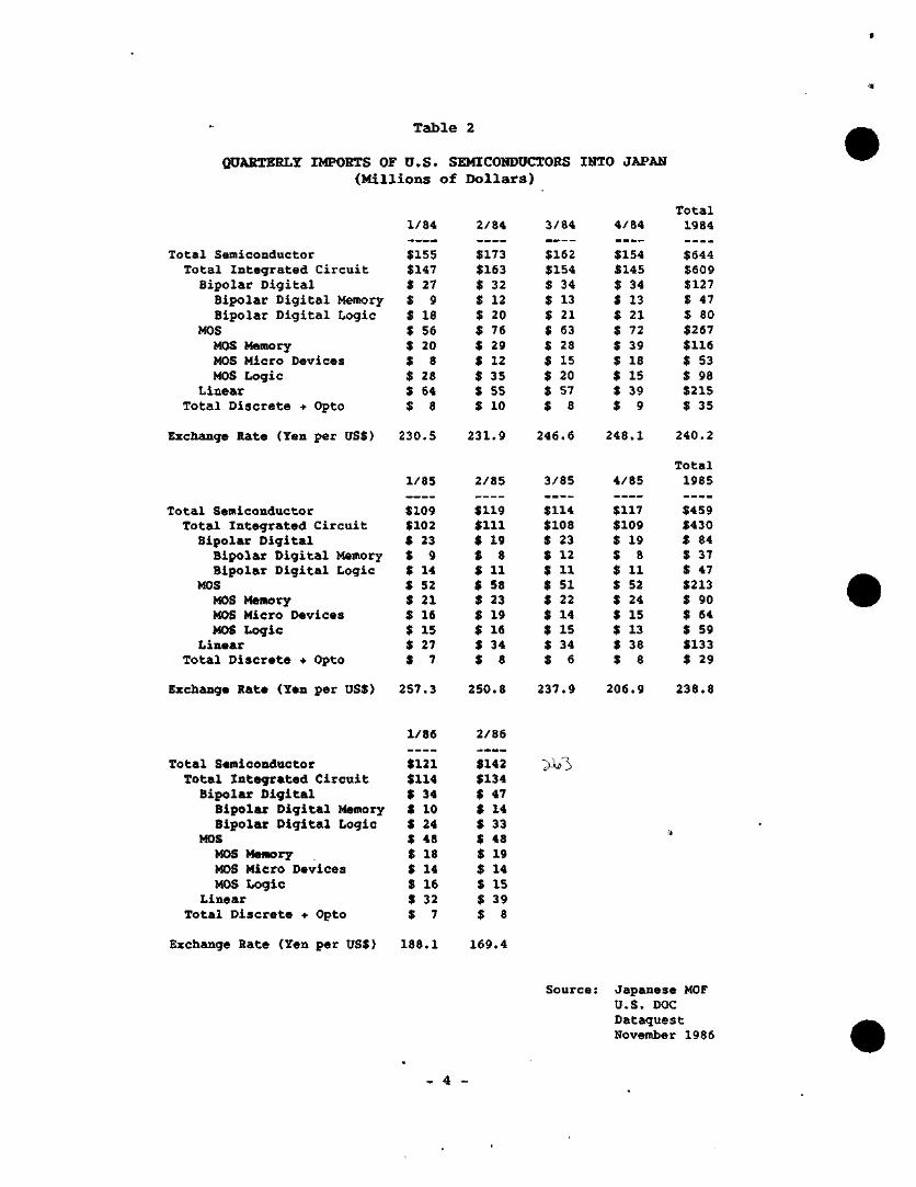
Table 2
QUARTERLY IMPORTS OF U.S. SEMICONDUCTORS INTO JAPAN (Millions of Dollars)
Total Semiconductor Total Integrated Circuit
Bipolar Digital Bipolar Digital Memory Bipolar Digital Logic
MOS MOS Memory MOS Micro Devices MOS Logic
Linear Total Discrete -i- Opto
1/84
$155 $147 $ 27 $ 9 $ 18 $ 56 $ 20 $ 8 $ 28 $ 64 $ 8
2/84
$173 $163 $ 32 $ 12 $ 20 $ 76 $ 29 $ 12 $ 35 $ 55 $ 10
3/84
$162 $154 $ 34 $ 13 $ 21 $ 63 $ 28 $ 15 $ 20 $ 57 $ 8
4/84
$154 $145 $ 34 $ 13 $ 21 $ 72 $ 39 $ 18 $ 15 $ 39 $ 9
Total 1984
$644 $609 $127 $ 47 $ 80 $267 $116 $ 53 $ 98 $215 $ 35
Exchange Rate (Yen per US$) 230.5 231.9 2 4 6 . 6 2 4 8 . 1 240 .2
Total Semiconductor Total Integrated Circuit Bipolar Digital Bipolar Digital Memory Bipolar Digital Logic
MOS MOS Memory MOS Micro Devices MOS Logic
Linear Total Discrete ••• Opto
1/85
$109 $102 $ 23 $ 9 $ 14 $ 52 $ 21 $ 16 $ 15 $ 27 $ 7
2/85
$119 $111 $ 19 $ 8 $ 11 $ 58 $ 23 $ 19 $ 16 $ 34 $ 8
3/85
$114 $108 $ 23 $ 12 $ 11 $ 51 $ 22 $ 14 $ 15 $ 34 $ 6
4/85
$117 $109 $ 19 $ 8 $ 11 $ 52 $ 24 $ 15 $ 13 $ 38 $ 8
Total 1985
$459 $430 $ 84 $ 37 $ 47 $213 $ 90 $ 64 $ 59 $133 $ 29
Exchange Rate (Yen per US$) 257.3 250.8 237.9 206.9 238.8
1/86 2/86
Total Semiconductor Total Integrated Circuit Bipolar Digital
Bipolar Digital Memory Bipolar Digital Logic
MOS MOS Memory MOS Micro Devices MOS Logic
Linear Total Discrete * Opto
$121 $114 $ 34 $ 10 $ 24 $ 48 $ 18 $ 14 $ 16 $ 32 $ 7
$142 $134 $ 47 $ 14 $ 33 $ 48 $ 19 $ 14 $ 15 $ 39 $ 8
>i^3
Exchange Rate (Yen per US$) 188.1 169.4
Source: Japanese MOF U.S. DOC Dataguest November 1986
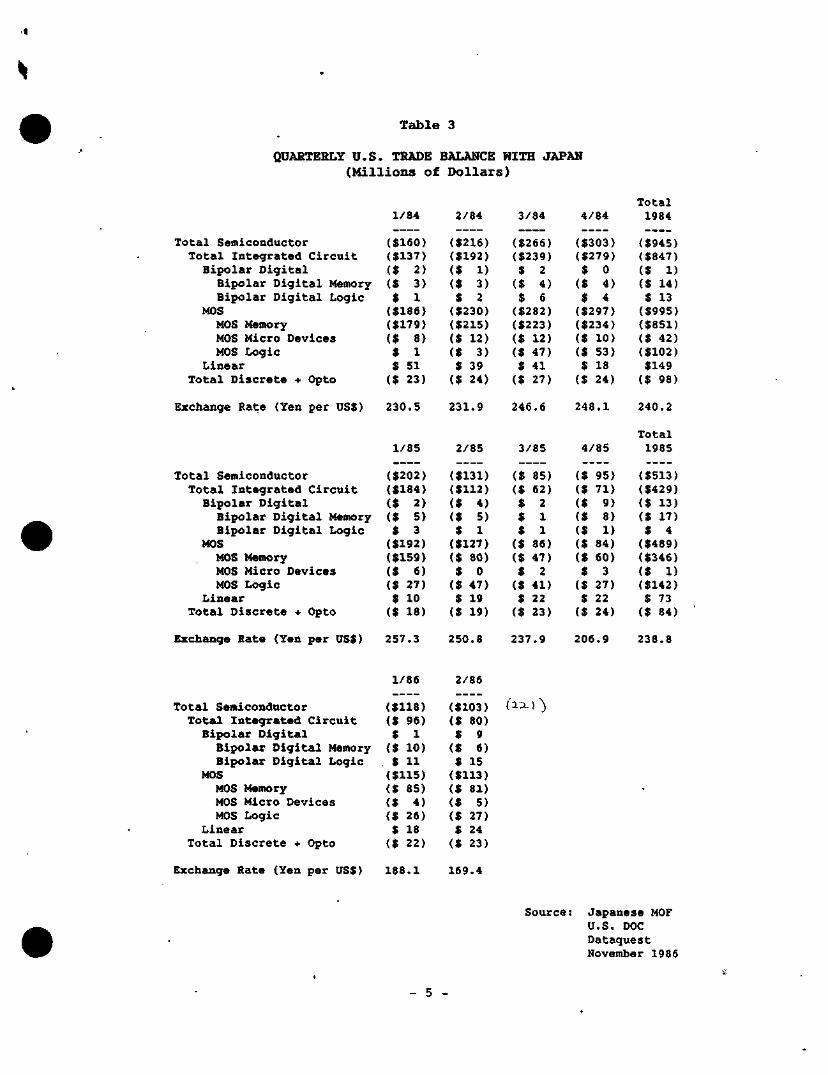
Table 3
QUARTERLY U.S. TRADE BALANCE WITH JAPAN ( M i l l i o n s of Dollars)
Total Semiconductor Total Integrated Circuit
Bipolar Digital Bipolar Digital Memory Bipolar Digital Logic
MOS MOS Memory MOS Micro Devices MOS Logic
Linear Total Discrete -i- Opto
1/84
($160) ($137) ($ 2) ($ 3) $ 1 ($186) ($179) ($ 8) $ 1 $ 51 ($ 23)
2/84
($216) ($192) ($ 1) ($ 3) $ 2 ($230) ($215) ($ 12) ($ 3) $ 39 ($ 24)
3/84
($266) ($239) $ 2 ($ 4) $ 6 ($282) ($223) ($ 12) ($ 47) $ 41 ($ 27)
4/84
($303) ($279) $ 0 ($ 4) $ 4 ($297) ($234) ($ 10) ($ 53) $ 18 ($ 24)
Total 1984
($945) ($847) ($ 1) ($ 14) $ 13 ($995) ($851) ($ 42) ($102) $149 ($ 98)
Exchange Rate (Yen per US$) 230.5 231.9 246.6 248.1 240.2
Total Semiconductor Total Integrated Circuit
Bipolar Digital Bipolar Digital Memory Bipolar Digital Logic
MOS MOS Memory MOS Micro Devices MOS Logic
Linear Total Discrete -t- Opto
1/85
($202) ($184) ($ 2) ($ 5) $ 3 ($192) ($159) ($ 6) ($ 27) $ 10 ($ 18)
2/85
($131) ($112) ($ 4) ($ 5) $ 1 ($127) ($ 80) $ 0 ($ 47) $ 19 ($ 19)
3/85
($ 85) ($ 62) $ 2 $ 1 $ 1 ($ 86) ($ 47) $ 2 ($ 41) $ 22 ($ 23)
4/85
($ 95) ($ 71) ($ 9) ($ 8) ($ 1) ($ 84) ($ 60) $ 3 ($ 27) $ 22 ($ 24)
Total 1985
($513) ($429) ($ 13) ($ 17) $ 4 ($489) ($346) ($ 1) ($142) $ 73 ($ 84)
Exchange Rate (7en per US$) 257.3 250.8 237.9 206.9 238.8
1/86 2/86
Total Semiconductor Total Integrated Circuit
Bipolar Digital Bipolar Digital Memory Bipolar Digital Logic
MOS MOS Memory MOS Micro Devices MOS Logic
Linear Total Discrete + Opto
($118) ($ 96) $ 1 ($ 10) $ 11 ($115) ($ 85) ($ 4) ($ 26) $ 18 ($ 22)
($103) ($ 80) $ 9 ($ 6) $ 15 ($113) ($ 81) ($ 5) ($ 27) $ 24 ($ 23)
( l^i-1 ^
Exchange Bate (Yen per US$) 188.1 169.4
Source: Japanese MOF U.S. DOC Dataguest November 1986
- 5 -
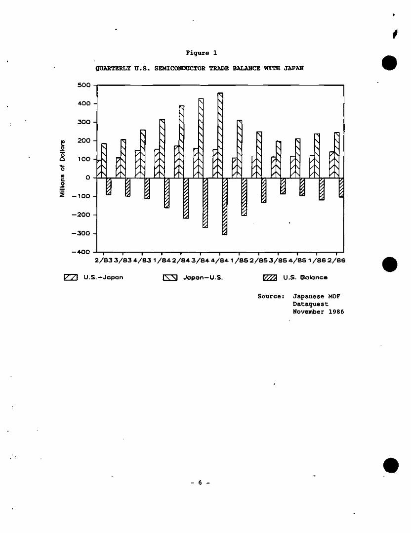
Figure 1
QUARTERLY U.S. SEMICONDUCTOR TRADE BALANCE WITH JAPAN
500
12
3 Q
.1
-4OO T I 1 1 ( I 1 1 1 1 r 2/83 3/83 4/83 1 /84 2/84 3/84 4/84 1 /85 2/85 3/85 4/85 1 /SB 2/86
1771 U.S.-Japan rsTs] J a p a n - U . S . P^?^ U.S. Balance
Source: Japanese MOF Dataguest November 1986
6 -
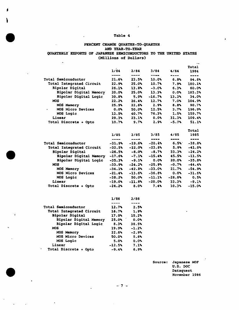
Table 4
PERCENT CHANGE QUARTER-TO-QUARTER AND YEAR-TO-YEAR
QUARTERLY ES>ORTS OF JAPANESE SEMICONDUCTORS TO THE UNITED STATES (M i l l ions of Do l la rs )
Total Semiconductor Total I n t e g r a t e d Circuit Bipolar Digital Bipolar Digital Memory Bipolar Digital Logic
MOS MOS Memory MOS Micro Devices MOS Logic
Linear Total Discrete -i- Opto
Total Semiconductor Total Integrated Circuit Bipolar Digital
B i p o l a r Digital Memory B i p o l a r Digital Logic
MOS MOS Memory MOS Micro Devices MOS Logic
Linear Total Discrete -»• Opto
1/84
21.6" 22.9% 26.1% 20.0% 30.8% 22.2% 25.9% 0.0% 12.5% 29.3% 10.7%
1/85
31.9% 32.5% 26.5% 17.6% 35.3% 33.9% 34.1% 21.4% 38.2% 19.0% 24.2%
2/84
23.5% 25.0% 13.8% 25.0% 5.9%
26.4% 22.6% 50.0% 40.7% 23.1% 9.7%
2/85
-19.6% -22.0% -8.0% -7.1% -9.1%
-24.2% -42.8% -13.6% 50.0%
-11.8% 8.0%
3/84
10.0% 10.7% -3.0% 13.3%
-16.7% 12.7% 2.9% 12.5% 76.3% 0.0% 2.9%
3/85
-20.4% -23.8% -8.7%
-15.4% 0.0%
-25.9% -33.0% -36.8% -11.1% -20.0% 7.4%
4/84
6.8% 7.9% 6.3% 0.0% 13.3% 7.0% 8.8% 3.7% 1.5%
31.3% -5.7%
4/85
6.5% 5.9%
33.3% 45.5% 20.0% -0.7% 21.7% 0.0%
-28.6% 33.3% 10.3%
Total 1984
94.8% 100.1% 60.0%
103.3% 34.0% 104.9% 90.7% 196.9% 159.7% 109.4% 51.1%
Total 1985
-38.8% -41.0% -24.2% -11.5% -35.8% -44.4% -54.9% -31.6% 0.5%
-9.1% -15.0%
1/86 2/86
Total Semiconductor Total Integrated Circuit
B i p o l a r Digital Bipolar Digital Memory Bipolar Digital Logic
MOS MOS Memory MOS Micro Devices MOS Logic
Linear Total Discrete + Opto
12.7% 16.7% 17.9% 25.0% 8.3%
19.9% 22.6% 50.0% 5.0%
-12.5% -9.4%
2.5% 1.9%
15.2% 0.0%
38.5% -1.2% -2.9% 5.6% 0.0% 7.1% 6.9%
Source: Japanese MOF U.S. DOC Dataguest November 1986
7 -
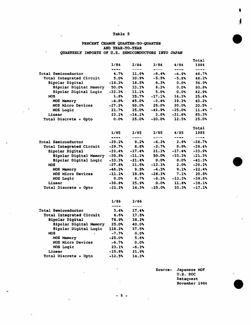
Table 5
PERCENT CHANGE QUARTER-TO-QUARTER AND YEAR-TO-YEAR
QUARTERLY IMPORTS OF U.S. SEMICONDUCTORS INTO JAPAN
Total Sem iconductor Total Integrated Circuit
Bipolar Digital Bipolar Digital Memory Bipolar Digital Logic
MOS MOS Memory MOS Micro Devices MOS Logic
Linear Total Discrete + Opto
Total Semiconducto r Total Integrated Circuit Bipolar Digital
B i p o l a r Digital Memory B i p o l a r Digital Logic
MOS MOS Memory MOS Micro Devices MOS Logic
Linear Total Discrete + Opto
1/84
4.7% 5.0%
-18.2% 50.0%
-33.3% 1.8%
-4.8% -27.3% 21.7% 23.1% 0.0%
1/85
-29.2% -29.7% -32.4% -30.8% -33.3% -27.8% -46.2% -11.1% 0.0%
-30.8% -22.2%
2/84
11.6% 10.9% 18.5% 33.3% 11.1% 35.7% 45.0% 50.0% 25.0% -14.1% 25.0%
2/85
9.2% 8.8%
-17.4% -11.1% -21.4% 11.5% 9.5% 18.8% 6.7%
25.9% 14.3%
3/84
-6.4% -5.5% 6.3% 8.3% 5.0%
-17.1% -3.4% 25.0% -42.9% 3.6%
-20.0%
3/85
-4.2% -2.7% 21.1% 50.0% 0.0%
-12.1% -4.3%
-26.3% -6.3% 0.0%
-25.0%
4/84
-4.9% -5.8% 0.0% 0.0% 0.0%
14.3% 39.3% 20.0%
-25.0% -31.6% 12.5%
4/85
2.6% 0.9%
-17.4% -33.3% 0.0% 2.0% 9.1% 7.1%
-13.3% 11.8% 33.3%
Total 1984
46.7% 48.2% 54.9% 80.8% 42.9% 25.4% 43.2% 20.5% 11.4% 85.3% 25.0%
Total 1985
-28.7% -29.4% -33.9% -21.3% -41.3% -20.2% -22.4% 20.8%
-39.8% -38.1% -17.1%
1/86 2/86
Total Semiconduc to r T o t a l Integrated Circuit
B i p o l a r Digital B i p o l a r Digital Memory B i p o l a r Digital Logic
MOS MOS Memory MOS Micro Devices MOS Logic
Linear Total Discrete -i- Opto
3.4% 4.6% 78.9% 25.0%
118.2% -7.7%
-25.0% -6.7% 23.1%
-15.8% -12.5%
17.4% 17.5% 38.2% 40.0% 37.5% 0.0% 5.6% 0.0%
-6.3% 21.9% 14.3%
Source: Japanese MOF U.S. DOC Dataguest November 1986
- 8 -
Dataquest iuontpunvol Ttu: IHin &'l)rij(Ktti:L<i Lorp^ytion
JAPANESE RESEARCH
NEWSLETTER
JSIS Code: Newsletters 1985-1986, JSIA 1986-47
SIGNIFICANT PRODUCT ANNOUNCEMENTS—GaAs ICs
Product development activity is accelerating in the GaAs industry. Important announcements have been made by several GaAs houses in recent months; this newsletter examines the most significant recent product introductions.
BIT SLICES—THE RACE IS ON
Vitesse introduced the first commercially available LSI GaAs digital IC set, an ECL lOOK compatible 4-bit slice family, on September 10, 1986, at Midcon. The product family consists of the VE29G01 4-Bit Microprocessor Slice, the VE29G02 Look-Ahead Carry Generator, and the VE29G10 Microcontroller. Engineering samples of the VE29G02 are available now, and engineering samples of the VE29G01 and VE29G10 are expected by February 1987. Earlier, McDonnell-Douglas released details on a 2901-type GaAs bit slice; however, McDonnell-Douglas is not a merchant market supplier of the device. Vitesse's product family is supported by a 3.5ns cycle 1024x4 registered static RAM, the VE12G474.
The VE29GXX family is expected to permit customers to achieve a factor of 3x speed improvement over a CPU implementation using the AMD2901C, a bipolar device. Interestingly, Vitesse has employed LCC packaging to preserve the device speed advantage at the system level as much as practical. Very aggressive forward pricing is available from Vitesse, allowing the user to project systems costs through 1990. So far, more than 1,000 customers have expressed interest in this product set. Dataquest expects a wide range of applications to make use of this technology, including minisupercomputers, "smart" high-speed instrumentation, DSPs and other military functions, arithmetic/logic accelerators, and high-speed graphics equipment.
© 1986 Dataquest Incorporated October—Reproduction Prohibited
The conlent of this report represents our interpretation and analysis of information generally available to the public or released by responsible individuals in the subject companies, bul is not guaranteed as to accuracy or completeness It does not contain material provided to us in confidence by our clients Individual companies reported on and analyzed by DATAQUEST, may be clients of this and/or other DATAQUEST services This information is not furnished in connection with a sale or offer to sell secunties or in connection with the solicitation of an offer to buy securities This firm and its parent and/or their officers, stockholders, or members of their families may from time to lime, have a long or short position in the securities mentioned and may sell or buy such securities
Taiyo Ginza Building / 7-14-16 Ginza, Chuo-ku / Tokyo 104, Japan / (03) 546-3191 / Telex J32768 1290 Ridder Park Drive / San Jose, CA 95131-2398 / (408) 971-9000 / Telex 171973
STATIC RAMs
For several months, IK SRAMs have been offered for beta site evaluation by GigaBit, Ford Microelectronics, and others. GigaBit just received a $500 thousand, two-year U.S.A.F. contract to perform Class 8 screening, reliability evaluation, and radiation hardness evaluation on its IK SRAM.
Vitesse's VE12G474 is the first commercially available 4K GaAs SRAM. Other announcements are expected this month, including devices from Honeywell, Rockwell, and GAIN. Several Japanese companies have been working on SRAMs for at least three years; these products appear targeted first for internal needs before being taken to merchant market. GaAs SRAMs feature cycle times in the 0.6 to 3.5ns range at IK and 4K densities, compared to the 5 to 7ns range for the fastest commercially available silicon ECL RAMs (see Table 1).
CUSTOM DESIGN
GAIN Electronics Corporation has announced a custom design service based initially on E/D MESFET technology and followed by SDHT (selectively doped heterostructure transistor), otherwise known as HEMT (high electron mobility transistor), technology. SDHT, invented by Dr. Raymond Dingle (GAIN'S president), offers the highest-performance commercially available GaAs circuitry. Typical transistor cutoff frequency is 80 GHz, versus 50 and 15 GHz, respectively, for GaAs FETs and Si bipolar transistors. GAIN will also offer a full line of device and design capabilities, and an epitaxial GaAs/ALGaAs wafer.
GigaBit Logic (GEL) has announced a standard cell library of D-MESFET logic blocks featuring 1/A geometries and 100 to 200ps gate delays at 1 to 2mW per gate. The initial family includes 13 macrocells, with 17 additional macros including a 4-bit adder planned for 1987. GigaBit charges $10,000 for its cell library diskette and user manual, refundable against the cost of the first development program.
MMICs
Dataquest believes that the most significant announcement in GaAs MMIC (microwave monolithic IC) technology in recent months is the introduction of a GaAs l i n e a r / a n a l o g macrocell library by Pacific Monolithics. The library consists of more than 25 macrocells fabricated and tested prior to July 1986, with another 20 macros in development. The cells cover the 0.5 to 18 GHz frequency range and include amplifiers, switches, combiners, splitters, attenuators, and VCOs (see Table 2).
Pacific Monolithics' macrocell library offers its users two major advantages. First, the design lead time, which ranges from 1 to 2-1/2 years for a custom MMIC, can be reduced by a factor of 2 to 5 using standard cells. Second, development cost is dramatically reduced, by a
- 2
factor of 3 to 8 fo r a typical MMIC design. Dataquest believes that Pacific Monolithic's library availability at this device performance level may radically alter the approach t o electronic warfare systems design. Furthermore, the approach may have a major impact on the entire present microwave industry structure, which includes hybrid houses, silicon device suppliers, third-party designers and other relatively expensive, time-consuming factors.
GATE ARRAYS
Honeywell, TriQuint, Texas Instruments, and others are deve loping gate arrays using GaAs technology. Honeywell recently withdrew its 2K gate array and is reportedly developing a standard cell alternative. Suppliers are polarizing into two camps regarding GaAs ASICs. One group is pursuing gate arrays of 400 to more than 5,000 gate density. The second group is proceeding on the basis that a standard cell solution will offer the best performance/cost trade-off to the user. Dataquest believes that sufficient applications exist to support both approaches, and expects additional announcements in this area in the coming months.
DATAQUEST CONCLUSIONS
The pace of GaAs product activity is quickening, spurred by major capital investments in 1984 and 1985 and by a soft electronics market in 1985 and 1986. Users have a growing variety of GaAs design options available, supported by an expanding infrastructure of suppliers. Dataquest believes that performance-oriented applications will gravitate at an accelerating rate toward the use of GaAs in critical hardware paths. Significant commercial systems house announcements based on the use of GaAs components are expected, starting in 1987.
Gene Miles
3 -
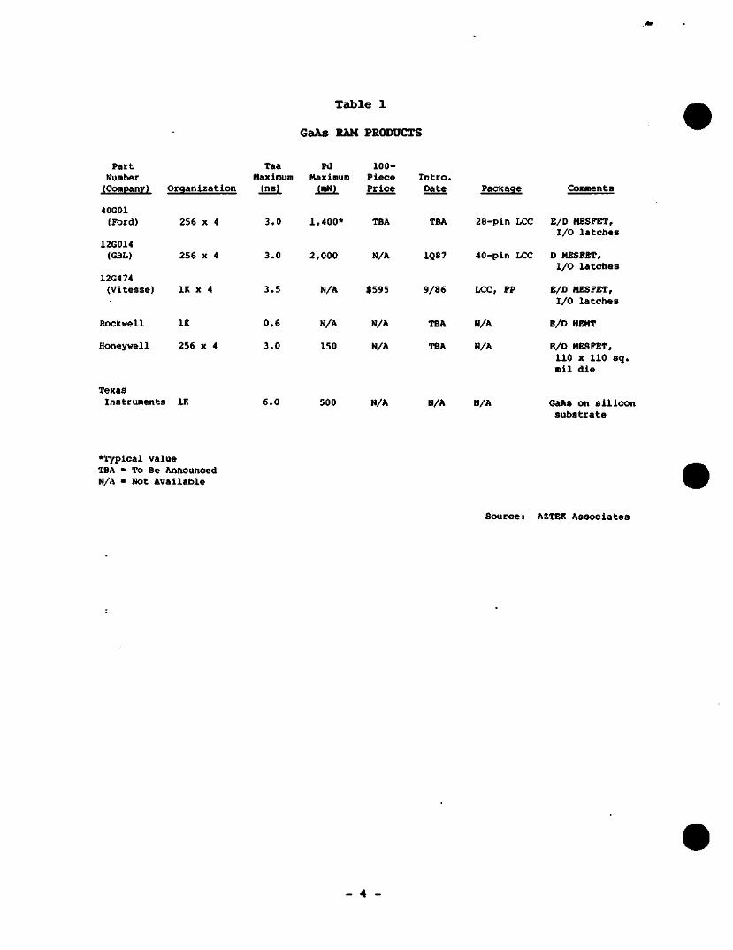
T a b l e 1
GaAs RAM PRODUCTS
Number (Company)
40G01 (Ford)
12G014 (GBL)
12G474 (Vitesse)
Rockwell
Honeywell
Organization
256 X 4
256 X 4
IK X 4
IK
256 X 4
Maximum (ns)
3.0
3.0
3.5
0.6
3.0
Maximum (mWJ
1,400*
2,000
N/A
N/A
150
Piece Price
TBA
N/A
$595
N/A
N/A
Intro Date
TBA
1Q87
9/86
TBA
TBA
Texas Instruments IK 6 . 0 500 N/A
Package Comments
2 8 - p i n LCC E/D MESFET, I / O l a t c h e s
4 0 - p l n LCC D MESFET, I / O l a t c h e s
LCC, FP
N/A
N/A
N/A N/A
E/D MESFET, I / O l a t c h e s
E/D HEMT
E/D MESFET, 110 x 110 sg. mil die
GaAs on silicon substrate
•Typical Value TBA = To Be Announced N/A " Not Available
Source: AZTEK Associates
4 -
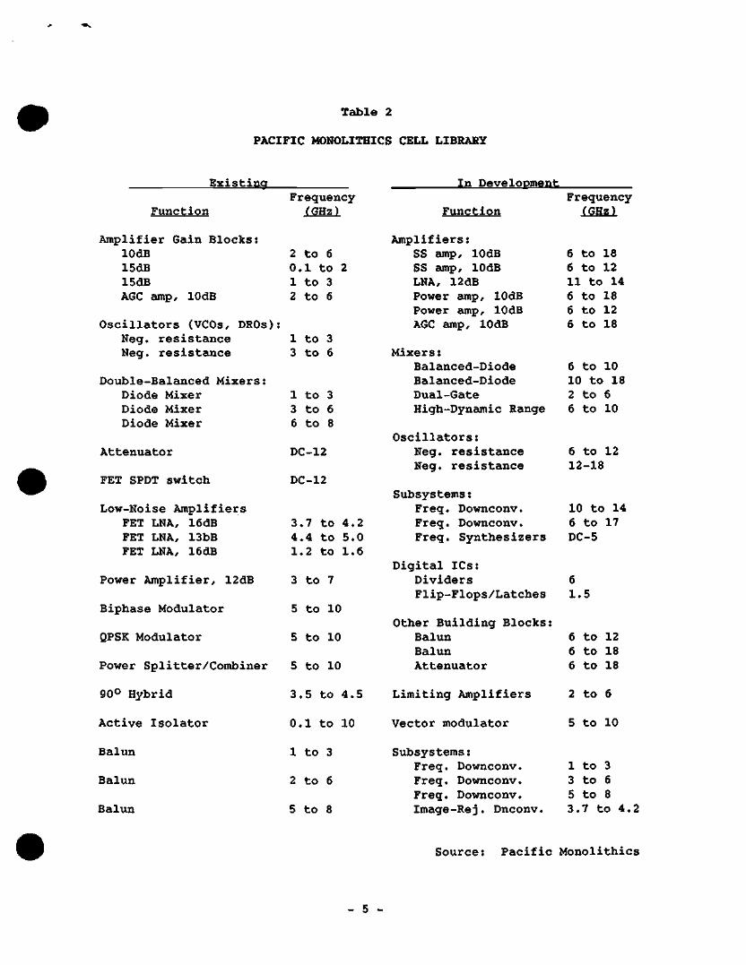
Table 2
PACIFIC MONOLITHICS CELL LIBRARY
Existing Frequency
Function (GHz)
Amplifier Gain Blocks: lOdB 2 to 6 15dB 0.1 t o 2 15dB 1 to 3 AGC amp, lOdB 2 to 6
Oscillators (VCOs, DROs): Neg. resistance 1 to 3 Neg. resistance 3 to 6
Double-Balanced Mixers: Diode Mixer 1 to 3 Diode Mixer 3 to 6 Diode Mixer 6 to 8
Attenuator DC-12
FET SPDT switch DC-12
Low-Noise Amplifiers FET LNA, 16dB 3.7 to 4.2 FET LNA, 13bB 4.4 to 5.0 FET LNA, 16dB 1.2 to 1.6
Power Amplifier, 12dB 3 to 7
Biphase Modulator 5 to 10
QPSK Modulator 5 to 10
Power Splitter/Combiner 5 to 10
90° Hybrid 3.5 to 4.5
Active Isolator 0.1 to 10
Balun 1 to 3
Balun 2 to 6
Balun 5 to 8
In Development
Function
Amplifiers: SB amp, lOdB SS amp, lOdB LNA, 12dB Power amp, lOdB Power amp, lOdB AGC amp, lOdB
Mixers: Balanced-Diode Balanced-Diode Dual-Gate High-Dynamic Range
Oscillators: Neg. resistance Neg. resistance
Subsystems: Freq. Downconv. Freq. Downconv. Freq. Synthesizers
Digital ICs: Dividers Flip-Flops/Latches
Other Building Blocks; Balun 6 to 12 Balun 6 to 18 Attenuator 6 to 18
Limiting Amplifiers 2 to 6
Vector modulator 5 to 10
Frequency
6 6 11 6 6 6
6
(GHz)
to to . to to to t o
t o
18 12 1 14 18 12 18
10 10 to 18 2 6
6
to to
to
6 10
12 12-18
10 to 14 6 to DC-5
6 1, .5
17
Subsystems: Freq. Downconv. Freq. Downconv. Freq. Downconv. Image-Rej. Dnconv.
1 to 3 3 to 6 5 to 8 3.7 to 4.2
Source: Pacific Monolithics
- 5 -
""'^'^ Conference Schedule
1986
Semiconductor
Tfechnical Computer
Asian Peripherals
Semiconductor Users/ Semiconductor Application
Markets
Electronic Publishing
CAD/CAM EDA
1987 Semiconductor Users/ Semiconductor Application
Markets
Copying and Duplicating
Electronic Printer
Japanese Semiconductor
Telecommunications
CAD/CAM
Display Terminals
European Semiconductor
European Copying and Duplicating
Financial Services
Western European Printer
European Telecommunications
Semiconductor
Office Equipment Dealers
Electronic Publishing
CAD/CAM EDA
October 20-22
November 3-5
November 5-7
November 10
November 17-18
December 4-5
February 4-6
February 23-25
March 23-25
April 13-14
April 13-15
May 14-15
May 20-22
June 4-5
June 25-26
August 17-18
September 9-11
October 1-2
October 19-21
November 5-6
November 16-17
December 10-11
Hotel Inter-Continental San Diego, California
Silverado Country Club Napa, California
Hotel Okura Tbkyo, Japan
Sheraton Harbor Island San Diego, California
Westin Copley Place Boston, Massachusetts
Santa Clara Marriott Santa Clara, California
Saddlebrook Resort Tampa, Florida
San Diego Hilton Resort San Diego, California
Silverado Country Club Napa, California
The Miyako Kyoto, Japan
Silverado Country Club Napa, California
Hyatt Regency Monterey Monterey, Csiifbmia
San Diego Hilton Resort San Diego, California
Palace Hotel Madrid, Spain
The Ritz Hotel Lisbon, Portugal
Silverado Country Club Napa, California
Palace Hotel Madrid, Spain
Monte Carlo, Monaco
The Fbinte Resort Phoenix, Arizona
Hyatt Regency Monterey, California
Stouffer Hotel Bedford, Massachusetts
Santa Clara Marriott Santa Clara, California
DataQuest Product Offerings
Industry Services
Business Computer Systems
CAD/CAM
Computer Storage—Rigid Disks
Computer Storage—Flexible Disks
Computer Storage—Tape Drives
Copying and Duplicating
Display Terminal
Electronic Printer
Electronic Publishing
Electronic Typewriter
Electronic Whiteboard
European Semiconductor*
European Telecommunications
Gallium Arsenide
Graphics
Imaging Supplies
Japanese Semiconductor*
Office Systems
Personal Computer
Personal Computer—Worldwide Shipments and Forecasts
Robotics
Semiconductor*
Semiconductor Application Markets*
Semiconductor Equipment and Materials*
Semiconductor User Information*
Software—Artificial Intelligence
Software—Personal Computer
Software-UNIX
Technical Computer Systems
Technical Computer Systems— Minisupercomputers
Telecommunications
Western European Printer
Executive and Financial Programs
Corporate Alliance Program
Coporate Technology Program
Financial Services Program
Strategic Executive Service
Newsletters
European PC Monitor
First Copy
Home Row
I.e. ASIA
I.e. USA
Focus Imports
The European PC Market 1985-1992
European PC Retail Pricing
PC Distribution in Europe
PC Software Markets in Europe
PC Local Area Networking Markets in Europe
The Education Market for PCs in Europe
Japanese Corporations in the European PC Markets
Home Markets for PCs in Europe
Integrated Office Systems— Tlie Market and Its Requirements
European Market for Text Processing
Image Processing in the Office
Work Group Computing
Translation Systems
Vendor Support
The IBM 3270 Market: 1986 and Beyond
Korean Semiconductor Industry Analysis
Diskettes—The Market and Its Requirements
Directory Products
I .e . Start-Ups-1987
SPECCHECK—Competitive Copier Guide
SPECCHECK—Competitive Electronic Typewriter Guide
SPECCHECK—Competitive Whiteboard Guide
Who's Who in CAD/CAM 1986
Future Products
• Industry Services
Manufacturing Automation Computer Storage—Optical Computer Storage—Subsystems
• Focus Reports
Japanese Printer Strategy Japanese Telecommunications
Strategy Canon CX Laser—User Survey Digital Signal Processing PC-based Publishing Taiwan Semiconductor Industry
Analysis China Semiconductor Industry
Analysis PC Distribution Channels
• Directory Products
SPECCHECK—Competitive Facsimile Guide
SPECCHECK—Competitive Electronic Printer Guide
•On-line delivery option available
For further information about these products, please contact your Dataquest sales representative or the Direct Marketing Group at (408) 971-9661.
rVtnlvr \QStf,
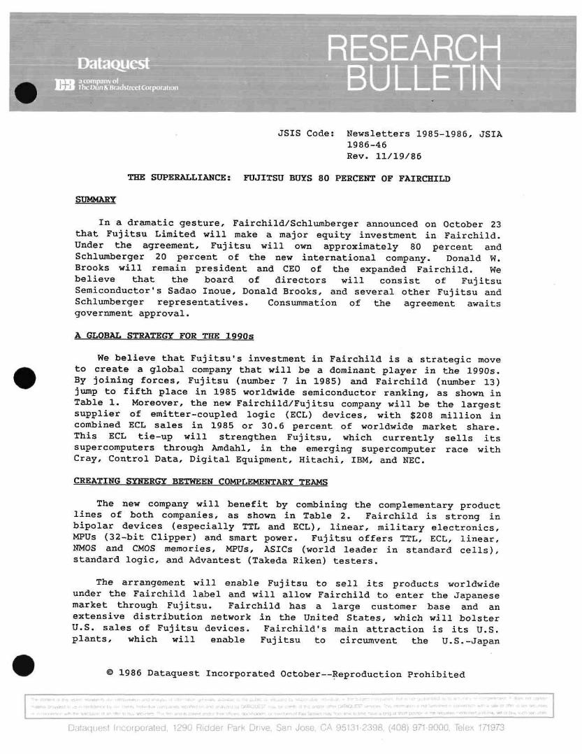
Dataquest aomipanvol ThcDun (t uracJsirutt Coqwraiion
RESEARCH BULLETIN
JSIS Code: Newsletters 1985-1986, JSIA 1986-46 Rev. 11/19/86
THE SUPERALLIANCE: FUJITSU BUYS 80 PERCENT OF FAIRCHILD
SUMMARY
In a dramatic gesture, Fairchild/Schlumberger announced on October 23 that Fujitsu Limited will make a major equity investment in Fairchild. Under the agreement, Fujitsu will own approximately 80 percent and Schlumberger 20 percent of the new international company. Donald W. Brooks will remain president and CEO of the expanded Fairchild. We believe that the board of directors will consist of Fujitsu Semiconductor's Sadao Inoue, Donald Brooks, and several other Fujitsu and Schlumberger representatives. Consummation of the agreement awaits government approval.
A GLOBAL STRATEGY FOR THE 1990s
We believe that Fujitsu's investment in Fairchild is a strategic move to create a global company that will be a dominant player in the 1990s. By joining forces, Fujitsu (number 7 in 1985) and Fairchild (number 13) jump to fifth place in 1985 worldwide semiconductor ranking, as shown in Table 1. Moreover, the new Fairchild/Fujitsu company will be the largest supplier of emitter-coupled logic (ECL) devices, with $208 million in combined ECL sales in 1985 or 30.6 percent of worldwide market share. This ECL tie-up will strengthen Fujitsu, which currently sells its supercomputers through Amdahl, in the emerging supercomputer race with Cray, Control Data, Digital Equipment, Hitachi, IBM, and NEC.
CREATING SYNERGY BETWEEN COMPLEMENTARY TjAMS
The new company will benefit by combining the complementary product lines of both companies, as shown in Table 2. Fairchild is strong in bipolar devices (especially TTL and ECL), linear, military electronics, MPUs (32-bit Clipper) and smart power. Fujitsu offers TTL, ECL, linear, NMOS and CMOS memories, MPUs, ASICs (world leader in standard cells), standard logic, and Advantest (Takeda Riken) testers.
The arrangement will enable Fujitsu to sell its products worldwide under the Fairchild label and will allow Fairchild to enter the Japanese market through Fujitsu. Fairchild has a large customer base and an extensive distribution network in the United States, which will bolster U.S. sales of Fujitsu devices. Fairchild's main attraction is its U.S. plants, which will enable Fujitsu to circumvent the U.S.-Japan
© 1986 Dataquest Incorporated October—Reproduction Prohibited
iiift ixrnBTH fl ur^ fcu^fT ^siTitfrf^ns
TnjIEIT.a &'JVII,1«t -U ^ >n Tt»llllVK(f
•••r n ^,-<<-<rf<l-Vi- *»rM V^ vK'M'- r t " - (t
v J ^
L'r
^ 1
• i i iM[hr*- i i ! i^ i iiJi
iTt i J n ' f t i i i^lIy
Ttlr" \ i n j v ^ ^ ?
1 if
t ^
IIF^
•^•^± i j l -i-Jvir
f < * ^ ^ v \ | i ^ f
•lUl'C*:
!i>yico
' •>-. iii+r i * i [ i i t h i ^ f ; '
^ ' i;ii'
llliillb, I^11,IILLM: VJ
-LTitJ jr-ii i. '.-L'.i t jv
1 ivi^y 1l "JJi U^Liir^
[lie pdbJtL ijs
tiw;^c^UJi!JT
flULt-hcJiDWi
^tlltJ[le^! tJ| •H.'-JLIIW
triLl> r>
Oi n i A i
tlieHL, <i\ ih
.rmd Wm.
-iljkf •iLhHiJi«)|:i
L ai\i>]L
^Tii|ie>j
»•• l l r f? 3\M'^'- •^•^
'Jl'i.n rwTaClL'Ea^ i j"uir ih
n* / . ' I ' j i ipiie tiliiTie ii(wii_
xini'T, tt,ini( r-£ff ajLiiTirteeJ 54^1 *
*^N^ 'iTinr'njifitTi 1 fxJ •iirT*'ii i?i3-n r.
Tl.r^'f IT- F^-^IJPflhTVt '* • llJff. tw ZUJ^ir
r nn:n<3T ju^-ri^ :,\i\it w s^f o i c i imuF'iici
i i y i f l Df nn fn'^pfM' iri *i(^r£Cumift!in'*rt'TiCT^^TMiTi»j ailrsi Uui Uj^ t l KV^^t^^
Dataqiiesl incorporated, 1290 Ridder Park Drive, San Jose, CA 95131-2398, (408) 971-9000, Telex 171973
semiconductor agreement by producing memories in the United States at Fairchild's plants. The recent U.S.-Japan semiconductor agreement seriously hurt Fujitsu's MOS memory sales by forcing it to sell DRAMs and EPROMs at high fair market values (FMVs).
THE STRATEGIC IMPLICATIONS
Although many observers fear that Fairchild is giving away its technology to Fujitsu, we believe that this agreement not only enables Fairchild to stay in the game, but will enable bot:h companies to become major global players in the 1990s by pooling their resources. Moreover, the U.S. Departunent of Defense will have access to Fujitsu's semiconductor and supercomputer technology through its procurement of Fairchild parts. The Japanese goverzunent recently agreed in principle to participate in the Strategic Defense Initiative (SDI). These agreements are the first in a series of closer U.S.-Japan commercial and military ties.
Sheridan Tatsuno Table 1
1985 WORLDWIDE RANKING OF SEMICONDUCTOR MAKERS (Millions of Dollars)
Ranlc
1 2 3 4 (5) 5 6
7/8 7/8 9 10
Comoany
NEC Motorola Iszas Instruments Hitachi Fujitsu/Fairchild Toshiba Phllips/Signetics Fujitsu Intel National Matsushita
Sources
Table 2
1985 BevenuB
$1,984 $1,830 $1,767 $1,671 $1,512 $1,468 $1,068 $1,020 $1,020 $ 943 $ 906
Dataquest October 1986
FAIRCHILD AND FUJITSU SEMICONDUCTOR REVENUE IN 1985 (Millions of Dollars)
Cateoorv
nicondttctors
Integrated Circuits Bipolar Digital
TTL ECL Other
MOS Memory Micro Devices Logic
Linear
Discrete
Optoelectronics
Fairchild
$492
451 329 257 68 4
22 4 10 8
100
39
2
Fu'tltan
$1 ,020
940 ' 267 111 140 16
631 412 106 113
42
37
43
Both
<1.512
1,391 596 368 208 20
653 416 116 121
142
76
45
Source:
WW Share
6.2%
7.5% 15.9% 1 1 . 9 % 3 0 . 6 % 12 .7%
6.5% 10.8% 4.3% 3.4%
3.0%
1.6%
3.7%
Dataquest October 1986
- 2 -
Dataquest a a company of
TtH-rKirt&BrndstrtctCoriHuraIItMi
RESEARCH BULLETIN
JSIS Code: Newsletters 1985-1986, JSIA 1986-45
FALLOUT FROM THE U.S.-JAPAN CHIP AGREEMENT: JAPAN'S SHIFT TO INNOVATIVE PRODUCTS
The recently signed U.S.-Japan Semiconductor Agreement has seriously impacted Japanese semiconductor makers and the worldwide memory market. Coming in the midst of a serious industry downturn and a 50 percent appreciation in the value of the yen, this agreement is forcing Japanese memory makers to rethink their corporate strategies. With the entry of South Korean and other Asian companies, Dataquest observes that Japanese chip makers are faced with a series of difficult challenges:
• Reducing their operating costs
• Eliminating excess fab capacity to lower the fair market values (FMVs) of their DRAMs and EPROMs
• Diversifying product portfolios
Building closer vendor-user ties
Buying more semiconductors from U.S. and European vendors
Developing innovative products and pursuing more creative research
We expect the "yen shock" to cause a massive restructuring of the Japanese economy during the next three to four years. Already, Japanese companies are shifting much of their commodity-oriented manufacturing to Southeast Asia and moving up the technology ladder to higher value-added products. Many Japanese companies have developed 5-year recovery plans.
The chip agreement will accelerate this shift to more innovative products. Initially, several Japanese vendors will be forced to abandon commodity memory markets and compete with U.S., European, and start-up companies in specialized memory markets and other non-commodity areas. Japanese companies are already diversifying into application-specific ICs (ASICs) and specialized microprocessors. Dataquest expects numerous changes in the structure of the Japanese semiconductor industry over time, as shown in Table 1.
1986 Dataquest Incorporated October—Reproduction Prohibited
The content of ttus renorl represents our interpretation and analysis of intormation qene'aily available !o ttie public c released t)y responsible individuals in Ihe subject companies bul ts not guaranteed as lo accuracy or completeness It aoes not contam
material provided io us m wnklence i)y our cliems Indn'idual companies reported on and analysed by CATAQUESF may be ^ lienis of this and/or olher DATAQUEST services Tfiis mformaiion is not lurmshed in connection wilti a sa'e or ofter to sell securities
or in connection with tl le sdiciiaiion ol an otier to buv securities This lirm and its oarent ana/or their officers siockholde's or memtxjrs ot their lamilpes may 'rom tme lo time tiave a long ot short positIon m the secunties uienlioned and miay sell o' buy sucf". securities
Dataquest Incorporated, 1290 Ridder Park Drive, San Jose, CA 95131-2398, (408) 971-9000, Telex 171973
Dataguest observes that the industry's center of gravity is guickly shifting to the Pacific Rim, which will account for 51 percent of worldwide s e m i c o n d u c t o r c o n s u m p t i o n in 1987. As this global shift occurs, it will be crucial for semiconductor companies to establish a strong marketing and R&D presence in Asia in order to maintain their global competitiveness.
Sheridan Tatsuno
Table 1
EXPECTED JAPANESE RESPONSES TO THE U.S.-JAPAN SEMICONDUCTOR AGREEMENT
Sliort-Term ( 1 - 2 years )
Long-Term (5 years)
Pricing Sharp FMV rise in Q3/1986, declining in Q4/1986
FMV pricing inversely related to capacity utilization
Lower prices in Japanese domestic market
Possible worldwide multitier pricing structure
OEM Activity
Vendor/OEM deals with rebates to lower FMVs
Opening of procurement offices in Tokyo and Seoul
Boardstuffing in Japan and more Asian production to remain price competitive
More U.S. captive fabs and alliances with start-ups
Assembly & Rapid Japanese shift to Asia Testing to cut costs
Massive shift of Japanese assembly and testing to Asia in all industries
Fab Capacity
Japanese vendors offer foundry More U.S. and European fabs capacity to increase plant utilization and reduce FMVs Older lines phased out and sold to emerging Asian countries
More fab agreements and joint ventures Modular fabs ($20-$50 million) with flexible manufacturing systems
Hew Japanese diversification into Products ASICs, MPUs, optoelectronics,
etc Emphasis on innovative new products (e.g., video memories)
Broadly diversified portfolio of high-value-added products
More ASIC design centers overseas
Basic R&O More R&D spending and basic RSiD labs
Accelerate national R&D projects and initiate new projects (e.g., synchrotron orbital radiation)
Push into highly focused creative research (AI parallel processors, biochips, specialized compilers, specialized MPUs, etc)
Hire more foreign researchers and open overseas R&D labs
Develop ties to foreign university R&D centers
Source: Dataguest October 1986
- 2 -
Dataquest acompaIryoF THL' l)ui>&'RnHi^rci.'1 CoFpoiiiIKiTi
RESEARCH BULLETIN
JSIS Code: Newsletters 1985-1986, JSIA 1986-44
NATIONAL CAPTIVATES ITS REPS
In a dramatic move on Monday, October 13, 1986, National Semiconductor made an offer to purchase its entire force of 150 to 200 U.S. sales representatives. Dataquest believes that this is an excellent move on the part of National and that it is also significant to the industry at large.
Currently, National's U.S. sales are almost exclusively through reps, while its European and Asian sales are handled by company employees. National is well along in its transition from a "jellybean" house to a firm with a broad line of proprietary products. Currently, more than 75 percent of National's new products are proprietary, and 18 of the top-selling 20 products are proprietary. National's component R&D expenditures have grown at a compound rate of 29 percent for the last three fiscal years and now stand at an estimated 19 percent of component revenue.
The acquisition of its North American sales force will permit National to better control its customer relations. This move represents a major push at National, where the corporate mission is to "provide service second to none—resulting in long-term National Semiconductor/ customer partnerships." Under National, this sales force should be able to better support the increasing complexity of the company's proprietary products and more effectively work with customers during long design-in cycles. Additionally, this offer is well timed because many reps are currently somewhat disheartened with their businesses. National should be able to acquire a direct sales force for much less than it could recruit and train one.
This action by National is worthy of note by other semiconductor firms since reps that sell National products no longer will sell other firms' products. Dataquest believes that the semiconductor industry is becoming more "globalized," with U.S. firms striving to enter the Japanese market and Japanese and European firms striving to enter the North American market. Given this increasingly competitive situation, access to a captive sales force could be a major advantage.
Patricia S. Cox Howard Z. Bogert
# 1986 Dataquest Incorporated October—Reproduction Prohibited
The conten', of this repori rGpresenlP, oin int(;rpfc!',a', cc a id analysiE cf nlorma'.or; generally available !o ine public or rele -iLe:! by 'P^pons'tile ndividuals 'n '.he subbed cnrrpamcs but Is nol quararteed as to accuracy o' compleleness It does noi conlam
malenal provided to us m (»nlidence by our clienls Individual companies reporled on and analyzed by CAfAQUESr may be clients of this and/or other DATAQUEST services Th:s mtormation is nol furnished ir> connection with a sale or offer to sell securities
or in conneclion writ the sc*iCilat.on ot an offer to buy securities This firm and its pareni and/or their officers siockfiofders or .'nerntefS ol the" Families may from tirne to tIme have a long or short position in the secunlies rnenlioned arid mIay sell or buy such securities
Dataquest Incorporated, 1290 Ridder Park Drive, San Jose, CA 95131-2398, (408) 971-9000, Telex 171973
DataQuest 3 {Lomyany ot the Oun&'Btacbtrccl Corpoiution
JAPANESE RESEARCH
NEWSLETTER
JSIS Code: News le t t e r s 1985-1986, JSIA 1986-43
IC CARDS: THE NEXT PC BOOM?
SHERIDAN M. TATSUNO Senior Industry Analyst
Japanese Semiconductor Industry Service
Dataquest Incorporated
At D a t a q u e s t ' s r e c e n t Semiconductor A p p l i c a t i o n Markets Focus Conference i n Santa C la ra , JSIS Senio r I n d u s t r y Ana lys t , Sher idan Tatsuno, gave a p r e s e n t a t i o n on IC card marke t a p p l i c a t i o n s and techno logy t r e n d s . A copy of h i s speech i s p r e s e n t e d on the pages t h a t fo l low.
1986 Dataques t I n c o r p o r a t e d Octobe r—Reproduct ion P r o h i b i t e d
The content o( this report represents our interpretation and analysis ol information generally available to the public or released by responsible individuals in the subject companies, but is not guaranteed as to accuracy or completenGss It does not contain material provided to us in conlidence by our clients Individual companies reported on and analyzed by DATAQUEST, may be clients ol this and/or other DATAOUEST services This information is not furnished in connection with a sale or offer to self securities or in connection with ttie solicitation ot an offer to buy securities This firm and its parent and/or their officers, stockholders, or memtaers of their families may from time to time, have a long or short position in the securities mentioned and may self or buy such securities
Taiyo Ginza Building / 7-14-16 Ginza, Chuo-ku / Tokyo 104, Japan / (03) 546-3191 / Telex J32768 1290 Ridder Park Drive / San Jose, CA 95131-2398 / (408) 971-9000 / Telex 171973
OVERVIEW
Applications
Technologies
Pricing trends
ISO standards
Europe
United States
Japan
During this industry downturn, semiconductor vendors have been seeking and developing new applications. Telecommunications, automotive electronics, compact disks, digital television, and minisupercomputers are attracting interest because of their immediate use and rapid growth potential. Less visible are IC cards, or "smart cards," which offer numerous applications and large market potential. However, because they require more long-term investments and a commitment to educating users, IC cards have been largely ignored by U.S. semiconductor makers.
Dataquest believes that IC cards will become a major end use in the 1990s, but it will be at least five years before we see large production runs. Until then, we will see numerous IC card tests worldwide and much trial and error. These conditions favor larger corporations with "patient money" or fast-moving start-ups that are willing to develop market niches. As a result, unless companies begin development now, they will be excluded from this future market.
- 2
IC CARD APPLICATIONS ("3M")
Market Sector
Military
Medical
Applications
"Dog tags" Procurement inventory
Health maintenance organizations (HMOs)
Kidney dialysis Biofeedback records
Manufacturing Inventory and process control Product testing records
Key points to note:
• Financial applications were the initial focus of IC card makers, but too many limitations, especially high costs and disagreements over standards, soured the market.
• The "3M" applications, which are not limited by standards and packaging requirements, will be the major thrust for IC cards during the next few years. They will be the catalyst for getting the financial side reinterested. There are serious problems here seeking IC solutions.
• Military: the U.S. Army is conducting a Soldier Data Tag Program at Fort Benjamin Harrison in Indiana. Another test is being conducted at Fort Lewis, Washington, from June 1986 to June 1987. The U.S. Army's goal is to eliminate paper records.
• Medical: IC cards can help solve major problems facing the medical industry: high administrative costs, malpractice insurance, redundant data handling, continuous care, and preventive care, especially among the elderly and non-English speaking groups.
• Manufacturing: This is a highly fragmented market that requires unique solutions. Generally, users are not knowledgeable about IC technology and require product families. Major applications are process and inventory control cards.
- 3 -
IC CARD APPLICATIONS (Continued)
Market Sector
Banking
Telecommunications
Office
Applications
Credit and cash cards* Access ID cards (vault)
Phone cards*
Personnel records Health insurance programs* Data access keycards* Sophisticated software Laser printers Intelligent photocopiers
•Currently being tested.
Key points to note:
• Banking, telecommunications, and office automation will require IC cards to increase security and reduce administrative costs. Starred (*) applications are currently being tested.
1-r Banking: Visa and MasterCard are testing credit and cash cards (see pages 20 to 21). ID cards could be used to control access into vaults and other high-security areas.
- Telecommunications: Phone cards are being tested in France but could be universally used for long-distance and international calls from public phone booths.
r. Office automation: IC cards could be used to keep records and reduce paperwork, especially for personnel, social security, health insurance, and training records. Future OA equipment may offer IC cards as portable, high-security memory storage devices using personalized identification numbers (PIN). Mitsubishi is developing a PC on a card.
- 4 -
IC CARD APPLICATIONS (Continued)
Market Sector
Hotels
Applications
Room ID key cards Check-in/out time records Reservations
Home Video games* Educational games (CAI) Utilities records
Automotive Driver's licenses Door ID key cards Car maintenance records*
*Currently being tested.
Key points to note:
• Hotels, homes, and automobiles offer potential IC card applications. Tests are already being conducted on video game software and car maintenance records.
Hotels: IC cards could be used to simplify reservations and monitor check-in/check-out times. IC key cards could be issued as "gold cards" by hotel chains for faster check-in/check-out.
Home: Video game software is already being put onto IC cards in Japan. In the future, IC cards could be issued by schools for educational purposes. Utility companies could issue IC cards as a simple way for homeowners to monitor their gas, water, heating, and air-conditioning bills on a daily basis.
Automotive: IC cards could be issued as driver's licenses with records of driving offenses, medical disabilities, and outstanding tickets. Door ID key cards could prevent car theft. Installed IC cards could be used to keep records of gas mileage, oil changes, tune-ups, odometer readings, and repairs.
IC CARD APPLICATIONS (Continued)
Market Sector Applications
Government Social Security records Food stamps* Tax records Commuter passes Voter registration
Schools Library cards Student transcripts*
Sports Personal training records Professional and collegiate team statistics and scorecards
•Currently being tested.
Key points to note:
• Government, schools and universities, and sports fans could become major users of IC cards.
- Government: The U.S. Department of Agriculture is testing IC cards to reduce food stamp fraud and waste. IC cards could also be used for tax payments, social security, and voter registration. Local governments could issue IC cards as library cards, commuter passes, and property tax records.
A major issue with government uses will be individual privacy due to the potential for surveillance.
Schools: The University of Paris VII is testing IC cards for student transcripts. IC cards could also be used as library cards, medical records, and student dormitory key cards.
Sports; Professional and amateur athletes could keep training and meet records in portable IC cards. "Football cards," "baseball cards," or "Olympics cards" with team and player statistics could be sold at retail stores during the season.
6 -
DRIVING FORCES
Search for the next PC
Demand-pull, not technology push
Convenience and portability
Data security
France-Japan-U.S. rivalry
Many applications not restricted by ISO packaging standards
Piggyback onto credit use
Key points to note:
• There are many market forces driving the development of IC cards. Probably the major factor is market demand for improved convenience, portability, and data security in the military, medical, and manufacturing areas.
• The strong rivalry between France, Japan, and the United States to commercialize inexpensive IC cards will accelerate their development.
• Unlike the financial area, the "3M" applications do not require ISO packaging standards before implementing IC cards. They can develop tailored, application-specific uses.
• Eventually, IC cards will supplement but not necessarily replace plastic credit cards. They may be "gold cards" that offer faster, better service, such as "speed lines" at crowded stores and more security.
7 -
CARD TECHNOLOGICAL EVOHJTION
Memory Density
Paper Card
Plastic Card
Human Readout
1 — ^ Machine Readout
Magnetic Records
Magnetic Stripe Card
Laser Card
10 Cards
IC Memory
Card
CPU • Memory
Source; Dataquest October 1986
Key points to note:
• IC cards represent a major technological evolution over existing plastic, magnetic stripe, and laser cards.
• Magnetic stripe cards, which have 1,200-bit capacity of binary data, offer easy read/write, but they have limited memory capacity and security protection.
• Laser cards will be used for large memory storage. Drexler, for example, has 20 licensees for its Drexon Card. But laser cards are hard to align and require very clean environments for writing, which eliminates many commercial and manufacturing applications.
• IC cards are divided into two types: memory cards and CPU cards. Memory cards will offer portability and micrographics capabilities, while CPU cards will offer processing functions.
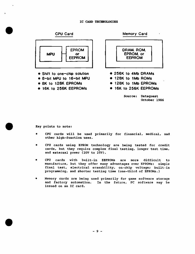
IC CARD TECHNOLOGIES
CPU Card Memory Card
MPU EPROM
or EEPROM
ORAM. ROM. EPROM. or
EEPROM
• Shift to one-chip solution • 8-bit MPU to 16-bit MPU • 8K to 128K EPROMs • 16K to 256K EEPROMs
• 256K to 4Mb DRAMs • 128K to 1Mb ROMs • 128K to 1Mb EPROMs • 16K to 256K EEPROMs
Source: Dataquest October 1986
Key points to n o t e :
• CPU cards will be used primarily for financial, medical, and other high-function uses.
• CPU cards using EPROM technology are being tested for credit cards, but they require complex final testing, longer test time, and external power (20V to 25V).
• CPU cards with built-in EEPROMs are more difficult to manufacture, but they offer many advantages over EPROMs: simple final test, electrical erasability, on-chip voltage; built-in programming, and shorter testing time (one-third of EPROMs.)
• Memory cards are being used primarily for game software storage and factory automation. In the future, PC software may be issued on an IC card.
- 9 -
CPU CARD APPLICATIONS
Type Applications
ISO Cash and credit cards Home banking Phone cards Medical cards Electronic messaging
Non-ISO Factory process control cards Company ID key cards Equipment maintenance cards
Key points to note:
• General applications, such as credit cards and phone cards, have broader market potential, but require ISO standards, which will limit their immediate commercialization.
• On the other hand, manufacturing only requires non-ISO cards for specific applications. Thus, Dataquest believes that non-ISO applications offer easier entry and earlier commercialization potential.
• If ISO standards are not quickly decided, many financial institutions may establish their own standards with other institutions.
- 10 ~
MEMORY CARD APPLICATIONS
Type
RAM -I-Battery
ROM (EPROM or EEPROM)
Applications
Personal computer data files Printer and typewriter disk files Television still photo files Digital sound storage cards
Game software Phone cards Dictionaries Factory records DA character files (Kanji)
Key points to note:
• Memory cards may eventually replace floppy disks for personal computer data files. Several Japanese companies are working on megabyte memory card prototypes, but they are still unproven.
• The weakness of memory cards is that they require a battery, but this obstacle could be overcome by lithium cell batteries being developed for on-chip and on-package use.
ROM cards offer a wide variety of applications, are its portability and convenience.
Key features
- 11 -
ANALOG CARD APPLICATIONS
Type Applications
MPU + Noncontact ID cards Analog (cars, f a c t o r i e s , offices)
Factory process and shipment control
Analog Noncontact ID cards
Key points to note:
• Noncontact analog cards offer solutions for access control (buildings, data banks, and computer rooms), supervision (laboratories, factories, and hospitals), and distribution (air freight and shipment of valuables).
• Analog cards, which are expected to replace magnetic cards, offer an automatic communication function, a sensor panel, control unit, and a register. The card automatically emits a signal that is received by the security control unit in entrances.
• In Japan, Arimura Institute of Technology is developing nontouch card systems that are being jointly marketed with Toshiba.
- 12
IC CARD PRICING FORECAST
Price ($) lOOn
MPU • 64K EEPROM Card
1985 1986 1987 1988 1989
Source: Dataquest October 1986
Key points to note:
• For volume p r o d u c t i o n to pick up, IC cards must become much cheaper. More efficient CAD design and manufacturing techniques will be required to move down the learning curve.
• CPU cards with a 16K EPROM will decline from their current price of $30 to less than $5 by 1990.
• Medical cards with an MPU and 64K EEPROM are expected to decline from more than $100 today to between $15 and $25 by 1990.
• Dataquest believes that Japanese vendors, especially printing companies, will be the price leaders.
- 13 -
ISO STANDARDS
ISO and American National Standards Institute (ANSI)
Physical characteristics
Size and thickness
Flexibility
- Durability
Dimension and location of contacts (CP8 French standard; top of card)
Electronic signals and exchange protocols (from 1987)
Key points to note:
• ISO standards are the major stumbling block to widespread use of IC cards. To date, the location of contacts has been decided; the French standard of having the IC in the top of the card will be followed.
* Another problem is that of achieving the goal of 30 mils thickness. CPU cards with BBPRCMs still cannot fit into these dimensions, so financial applications will be limited. However, CPU + EPREM cards are being developed and poised for growth.
• - 14 -
IMDUSO^Y SCORECARD
Tests Completed Tests Under Way Test Cards Card Types Vendors
Western Europe
8 19 lOKs 5 4
Asia/ Japan
0 19 IKs 44 81
Source:
North America
3 3 I to lOKs 7 6
Dataquest October 1985
Key points to note:
• To date, II IC card tests have been completed worldwide, mostly in France.
• However, 81 Japanese vendors are conducting some 19 experiments or more to develop the market. The Ministry of International Trade and Industry (MITI) has set up an ISO standards committee to promote industry agreement over standards. The Ministry of Posts and Telecommunications (MPT) and the Ministry of Finance (MOF) are working with banks to introduce cash, credit, and phone cards.
• Unlike Europe and Japan, the major IC card tests in the United States are sponsored by large corporations, such as Visa and MasterCard.
15
MAJOR PLAYERS IN EUROPE
Company Country Ties or Subsidiaries
Bull Group Crouzet Flonic-Schlumberger MasterCard
Multimil Perroux Philips Siemens Steria/Thomson
France France France United States
Switzerland France Netherlands West Germany France
MicroCard (U.S.); Olivetti Toshiba Paymatek (France) Credit Agricole and Credit Mutuel (France) Paytel TV (U.K.) Datacard (U.S.) TRT Telecommunications Dai Nippon Printing (Japan) Carte Bancaire (France)
Source! Dataquest October 1986
Key points to note:
• The French are the inventors and innovators of IC cards. By the end of 1986, France will have the following infrastructure in place: 4 million POS and phone cards (16 million by 1988), 52,000 POS terminals, 50,000 certifiers ordered, 30,000 phone booths, 56,000 card readers, and 8,200 card dispensers.
• The French effort is driven by several factors: the government emphasis on computerization/ telematigue (videotex and IC cards), and more efficient check processing.
• Major players are th© Bull Group, Crouzet, and Flonic-Schliunberger.
- 16
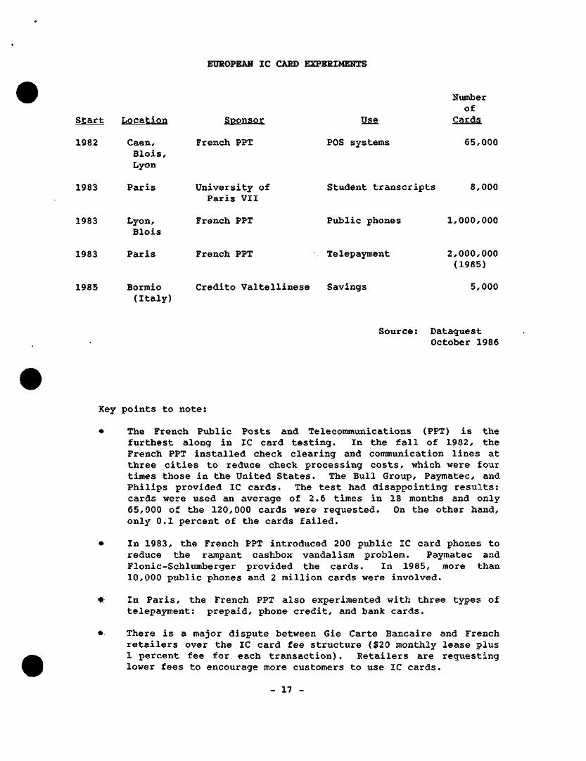
EUROPEAN IC CARD EXPERIMENTS
Start
1982
1983
Location
Caen, Blois, Lyon
Paris
Sponsor
French PPT
University of Paris VII
1983
1983
1985
Lyon, Blois
Paris
Bormio (Italy)
French PPT
French PPT
Use
POS systems
Student transcripts
Public phones
Telepayment
Credito Valtellinese Savings
Number of
Cards
65,000
8,000
1,000,000
2,000,000 (1985)
5,000
Source: Dataquest October 1986
Key points to note:
• The French Public Posts and Telecommunications (PPT) is the furthest along in IC card testing. In the fall of 1982, the French PPT installed check clearing and communication lines at three cities to reduce check processing costs, which were four times those in the United States. The Bull Group, Paymatec, and Philips provided IC cards. The test had disappointing results: cards were used an average of 2.6 times in 18 months and only 65,000 of the 120,000 cards were requested. On the other hand, only 0.1 percent of the cards failed.
• In 1983, the French PPT introduced 200 public IC card phones to reduce the rampant cashbox vandalism problem. Paymatec and Flonic-Schlumberger provided the cards. In 1985, more than 10,000 public phones and 2 million cards were involved.
• In Paris, the French PPT also experimented with three types of telepayment: prepaid, phone credit, and bank cards.
• There is a major dispute between Gie Carte Bancaire and French retailers over the IC card fee structure ($20 monthly lease plus 1 percent fee for each transaction). Retailers are requesting lower fees to encourage more customers to use IC cards.
- 17 -
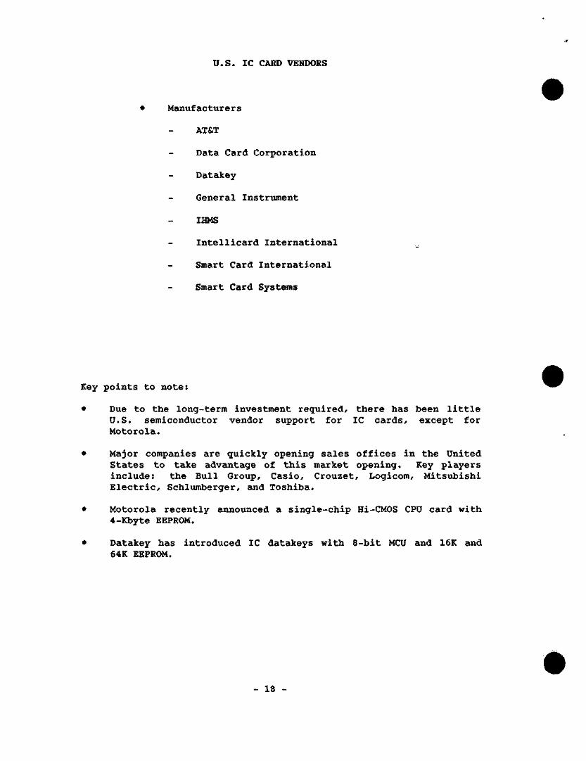
U.S. IC CARD VENDORS
Manufacturers
AT&T
Data Card Corporation
Datakey
General Instrument
Iffl<CS
Intellxcard I n t e r n a t i o n a l
Smart Card International
Smart Card Systems
Key points to note:
• Due to the long-term investment required, there has been little U.S. semiconductor vendor support for IC cards, except for Motorola.
• Major companies are quickly opening sales offices in the United States to take advantage of this market opening. Key players include: the Bull Group, Casio, Crouzet, Logicom, Mitsubishi Electric, Schlumberger, and Toshiba.
• Motorola recently announced a single-chip Hi-CMOS CPU card with 4-Kbyte EEPROM.
• Datakey has introduced IC datakeys with 8-bit MCU and 16K and 64K EEPROM.
18
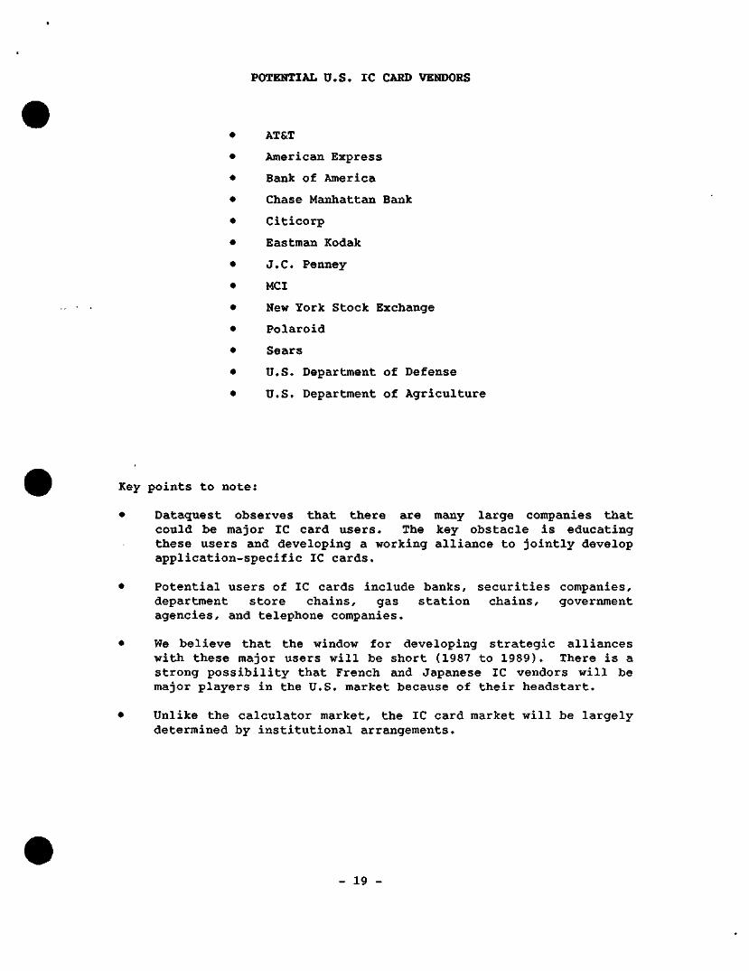
POTENTIAL U.S. IC CARD VENDORS
AT&T
American Express
Bank of America
Chase Manhattan Bank
Citicorp
Eastman Kodak
J.C. Penney
MCI
New York Stock Exchange
Polaroid
Sears
U.S. Department of Defense
U.S. Department of Agriculture
Key points to note:
• Dataguest observes that there are many large companies that could be major IC card users. The key obstacle is educating these users and developing a working alliance to jointly develop application-specific IC cards.
• Potential users of IC cards include banks, securities companies, department store chains, gas station chains, government agencies, and telephone companies.
• We believe that the window for developing strategic alliances with these major users will be short (1987 to 1989). There is a strong possibility that French and Japanese IC vendors will be major players in the U.S. market because of their headstart.
• Unlike the calculator market, the IC card market will be largely determined by institutional arrangements.
- 19 -
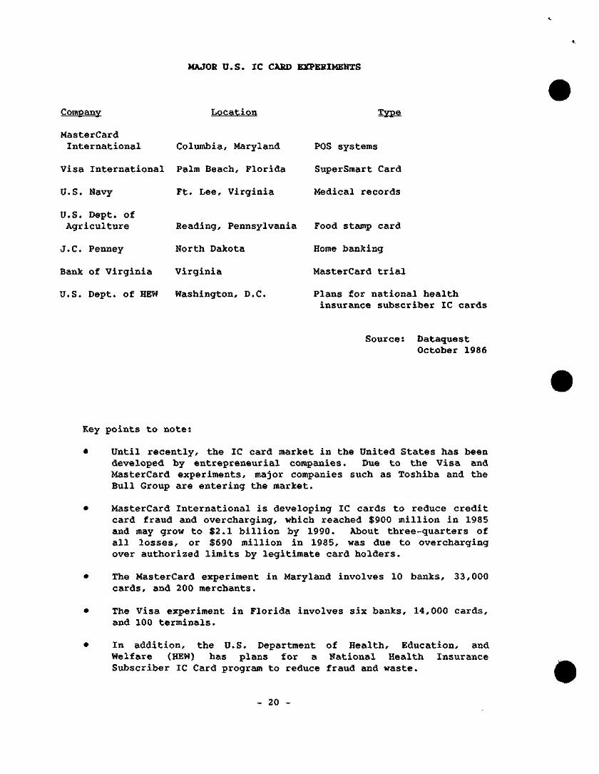
MAJOR U.S. IC CARD EXPERIMENTS
Company
MasterCard International
Location
Columbia, Maryland
Visa International Palm Beach, Florida
U.S. Navy
U.S. Dept. of Agriculture
J.C. Penney
Bank of Virginia
Ft. Lee, Virginia
Type
PCS systems
SuperSmart Card
Medical records
Reading, Pennsylvania Food stamp card
North Dakota
Virginia
U.S. Dept. of HEW Washington, D.C.
Home banking
MasterCard trial
Plans for national health insurance subscriber IC cards
Source: Dataguest October 1986
Key points to note:
• Until recently, the IC card market in the United States has been developed by entrepreneurial companies. Due to the Visa and MasterCard experiments, major companies such as Toshiba and the Bull Group are entering the market.
• MasterCard International is developing IC cards to reduce credit card fraud and overcharging, which reached $900 million in 1985 and may grow to $2.1 billion by 1990. About three-quarters of all losses, or $690 million in 1985, was due to overcharging over authorized limits by legitimate card holders.
• The MasterCard experiment in Maryland involves 10 banks, 33,000 cards, and 200 merchants.
• The Visa experiment in Florida involves six banks, 14,000 cards, and 100 terminals.
• In addition, the U.S. Department of Health, Education, and Welfare (HEW) has plans for a National Health Insurance Subscriber IC Card program to reduce fraud and waste.
- 20 -
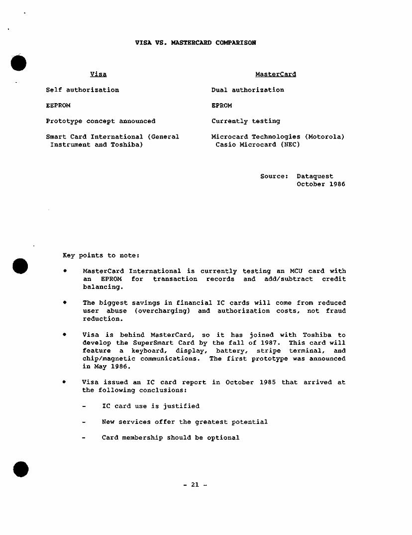
VISA VS. MASTERCARD COMPARISON
Visa
Self authorization
EEPROM
Prototype concept announced
Smart Card International (General Instrument and Toshiba)
MasterCard
Dual authorization
EPROM
Currently testing
Microcard Technologies (Motorola) Casio Microcard (NEC)
Source: Dataquest October 1986
Key points to note:
• MasterCard International is currently testing an MCU card with an EPROM for transaction records and add/subtract credit balancing.
• The biggest savings in financial IC cards will come from reduced user abuse (overcharging) and authorization costs, not fraud reduction.
• Visa is behind MasterCard, so it has joined with Toshiba to develop the SuperSmart Card by the fall of 1987. This card will feature a keyboard, display, battery, stripe terminal, and chip/magnetic communications. The first prototype was announced in May 1986.
• Visa issued an IC card report in October 1985 that arrived at the following conclusions:
IC card use is justified
New services offer the greatest potential
Card membership should be optional
- 21
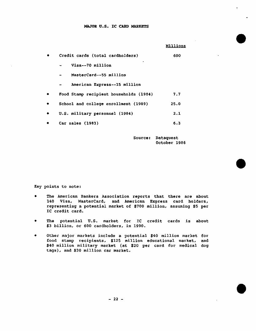
MAJOR U.S. ZC CARD MARKETS
Millions
Credit cards (total cardholders) 600
Visa—70 million
MasterCard—55 million
American Express—15 million
Food Stamp recipient households (1984) 7.7
School and college enrollment (1989) 25.0
U.S. military personnel (1984) 2.1
Car sales (1983) 6.3
Source: Dataquest October 1986
Key points to note:
• The American Bankers Association reports that there are about 140 Visa, MasterCard, and American Express card holders, representing a potential market of $700 million, assuming $5 per IC credit card.
• The potential U.S. market for IC credit cards is about $3 billion, or 600 cardholders, in 1990.
• Other major markets include a potential $40 million market for food stamp recipients, $125 million educational market, and $40 million military market (at $20 per card for medical dog tags), and $30 million car market.
- 22 -
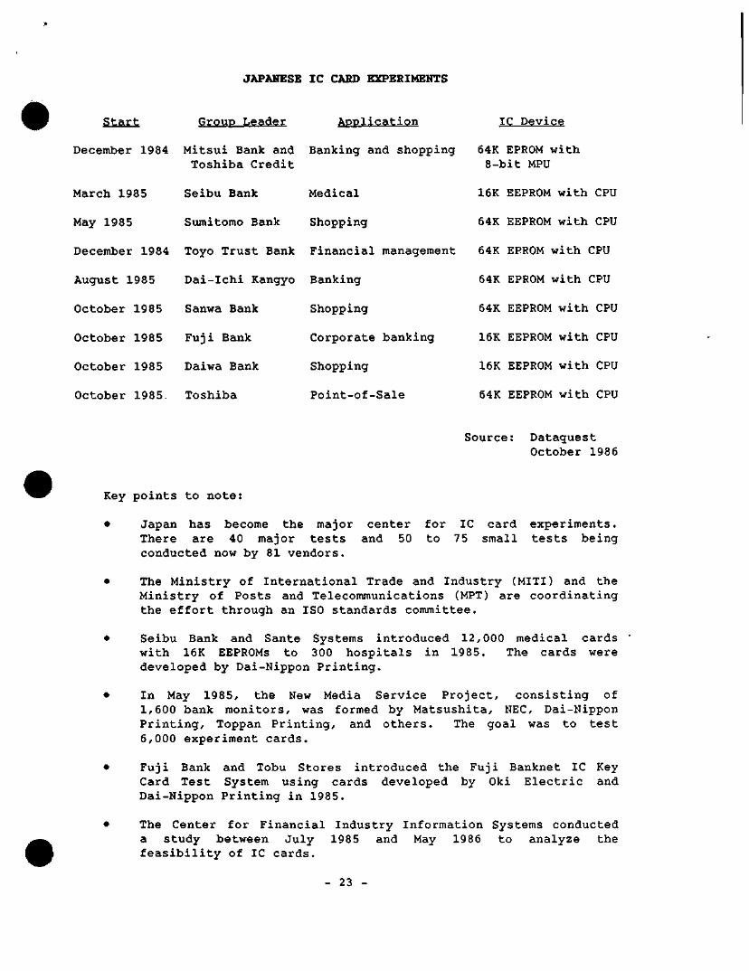
JAPANESE IC CARD EXPERIMENTS
Start
December 1984
March 1985
May 1985
December 1984
August 1985
October 1985
October 1985
October 1985
October 1985.
Group Leader Application
Mitsui Bank and Banking and shopping Toshiba Credit
Seibu Bank Medical
Sumitomo Bank Shopping
Toyo Trust Bank Financial management
Dai-Ichi Kangyo Banking
Sanwa Bank Shopping
Fuji Bank Corporate banking
Daiwa Bank Shopping
Toshiba Point-of-Sale
IC Device
64K EPROM with 8-bit MPU
16K EEPROM with CPU
64K EEPROM with CPU
64K EPROM with CPU
64K EPROM with CPU
64K EEPROM with CPU
16K EEPROM with CPU
16K EEPROM with CPU
64K EEPROM with CPU
Source: Dataguest October 1986
Key points to note:
• Japan has become the major center for IC card experiments. There are 40 major tests and 50 to 75 small tests being conducted now by 81 vendors.
• The Ministry of International Trade and Industry (MITI) and the Ministry of Posts and Telecommunications (MPT) are coordinating the effort through an ISO standards committee.
• Seibu Bank and Sante Systems introduced 12,000 medical cards with 16K EEPROMs to 300 hospitals in 1985. The cards were developed by Dai-Nippon Printing.
• In May 1985, the New Media Service Project, consisting of 1,600 bank monitors, was formed by Matsushita, NEC, Dai-Nippon Printing, Toppan Printing, and others. The goal was to test 6,000 experiment cards.
• Fuji Bank and Tobu Stores introduced the Fuji Banknet IC Key Card Test System using cards developed by Oki Electric and Dai-Nippon Printing in 1985.
• The Center for Financial Industry Information Systems conducted a Study between July 1985 and May 1986 to analyze the feasibility of IC cards.
23
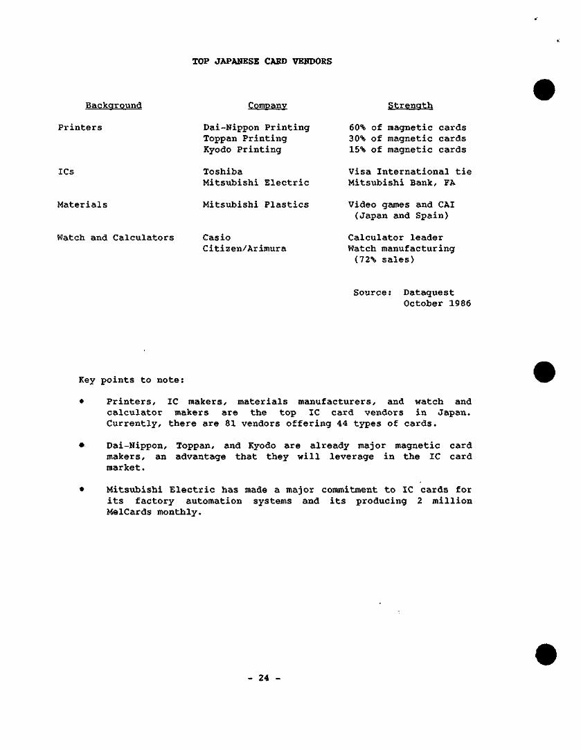
TOP JAPANESE CARD VENDORS
Background
Printers
ICs
Materials
Watch and Calculators
Company
Dai-Nippon Printing Toppan Printing Kyodo Printing
Toshiba Mitsubishi Electric
Mitsubishi Plastics
Casio Citizen/Arimura
Strength
60% of magnetic cards 30% of magnetic cards 15% of magnetic cards
Visa International tie Mitsubishi Bank, FA
Video games and CAI (Japan and Spain)
Calculator leader Watch manufacturing (72% sales)
Source: Dataquest October 1986
Key points to note:
• Printers, IC makers, materials manufacturers, and watch and calculator makers are the top IC card vendors in Japan. Currently, there are 81 vendors offering 44 types of cards.
• Dai-Nippon, Toppan, and Kyodo are already major magnetic card makers, an advantage that they will leverage in the IC card market.
• Mitsubishi Electric has made a major commitment to IC cards for its factory automation systems and its producing 2 million MelCards monthly.
24 -
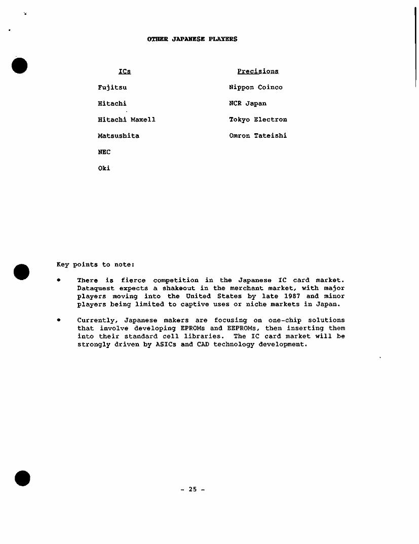
OTHER JAPANESE PLAYERS
ICs Precisions
Fujitsu Nippon Coinco
Hitachi NCR Japan
Hitachi Maxell Tokyo Electron
Matsushita Omron Tateishi
NEC
Oki
Key points to note:
• There is fierce competition in the Japanese IC card market. Dataquest expects a shakeout in the merchant market, with major players moving into the United States by late 1987 and minor players being limited to captive uses or niche markets in Japan.
• Currently, Japanese makers are focusing on one-chip solutions that involve developing EPROMs and EEPROMs, then inserting them into their standard cell libraries. The IC card market will be strongly driven by ASICs and CAD technology development.
25
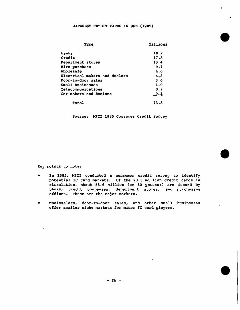
JAPANESE CREDIT CARDS IN USE (1985)
Type
Banks Credit Department stores Hire purchase Wholesale Electrical makers and dealers Door- to-door sales Small businesses Telecommunications Car makers and dealers
Millions
18.2 17.3 13.4 9.7 4.6 4.3 3.6 1.9 0.2 0.1
Total 73.3
Source: MITI 1985 Consumer Credit Survey
Key points to note:
• In 1985, MITI conducted a consumer credit survey to identify potential IC card markets. Of the 73.3 million credit cards in circulation, about 58.6 million (or 80 percent) are issued by banks, credit companies, department stores, and purchasing offices. These are the major markets.
• Wholesalers, door-to-door sales, and other small businesses offer smaller niche markets for minor IC card players.
26 -
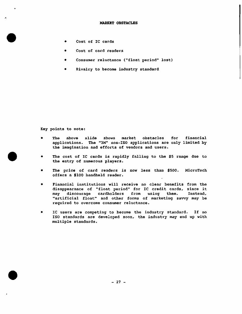
MARB:ET OBSTACLES
Cost of IC cards
Cost of card readers
Consumer reluctance ("float period" lost)
Rivalry to become industry standard
Key points to note:
• The above slide shows market obstacles for financial applications. The "3M" non-ISO applications are only limited by the imagination and efforts of vendors and users.
• The cost of IC cards is rapidly falling to the $5 range due to the entry of numerous players.
• The price of card readers is now less than $500. MicroTech offers a $100 handheld reader.
• Financial institutions will receive no clear benefits from the disappearance of "float period" for IC credit cards, since it may discourage cardholders from using them. Instead, "artificial float" and other forms of marketing savvy may be required to overcome consumer reluctance.
• IC users are competing to become the industry standard. If no ISO standards are developed soon, the industry may end up with multiple standards.
- 27 -
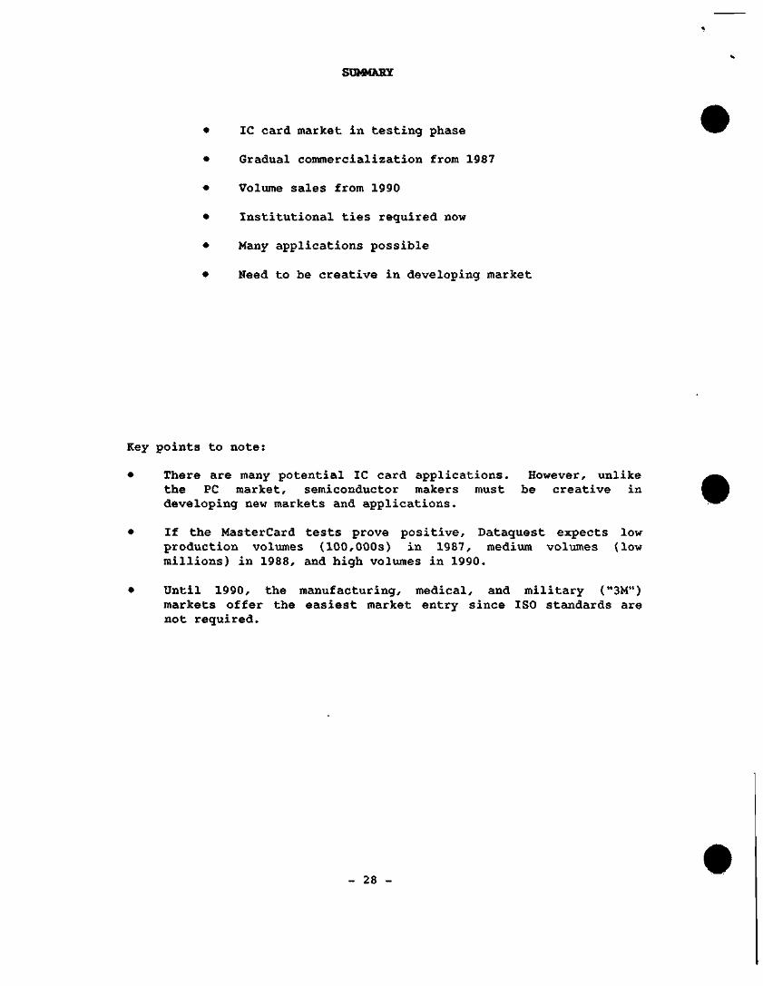
srooiARY
IC card market in testing phase
Gradual comme rc ia l i za t ion from 1987
Volume sales from 1990
Institutional ties required now
Many applications possible
Need to be creative in developing market
Key points to note:
• There are many potential IC card applications. However, unlike the PC market, semiconductor makers must be creative in developing new markets and applications.
• If the MasterCard tests prove positive, Dataquest expects low production volumes (100,000s) in 1987, medium volLimes (low millions) in 1988, and high volumes in 1990.
• Until 1990, the manufacturing, medical, and military ("3M") markets offer the easiest market entry since ISO standards are not required.
28
DataQuest ucompanvol The 1 )un S' Briidsl tcL-I tor porj! io( I
JAPANESE RESEARCH
NEWSLETTER
JSIS Code: Newsletters 1985-1986, JSIA 1986-42
JAPANESE SEMICONDUCTOR MARKET QUARTERLY UPDATE: HIGH YEN MASKS A DEPRESSED MARKET
SUMMARY
Nearly everything we said in our August market update newsletter (JSIS Niunber 1986-33, "Japanese Semiconductor Market Quarterly Update: High Yen Wreaking Havoc on Japanese Consumption") is still true. However, we are sufficiently pessimistic about what those things mean that we have revised our third and fourth quarter 1986 and most of 1987 projections downward from the last forecast.
We believe that the Japanese semiconductor market will grow 40.6 percent in dollars, this year, followed by a 19.4 percent increase in 1987. In terms of yen, however, the Japanese market—which grew only 1.1 percent in first quarter 1986 and 1.4 percent in second quarter 1986—will experience negative growth in both third and fourth quarter 1986, resulting in a decline of 2.0 percent for the year.
We have used actual exchange rates for the first three quarters of 1986: ¥188, ¥170, and ¥155 per dollar, respectively. The ¥155 exchange rate is carried forward through fourth quarter 1986 and through the four quarters of 1987.
Figure 1 shows quarter-to-guarter percent growth in yen for the Japanese semiconductor market from the first quarter of 1985 through the fourth quarter of 1987. Figure 2 presents the same data in dollars. A comparison of these two graphs shows that the dramatic ascent of the yen makes a depressed industry appear to be undergoing strong growth when expressed in dollars.
FORECAST
Our quarterly forecast, in both yen and dollars, is shown in Tables 1 through 4.
We expect to see a healthier market in 1987, as the painful adjustment period accompanying the yen's rise ends and the market begins to Stabilize. We believe that the total Japanese semiconductor market will grow 11.4 percent in yen in 1987, or 19.4 percent in dollars.
© 1986 Dataquest Incorporated October—Reproduction Prohibited
The content of this report represents our interpretation and analysis of information generally available to the public or released by responsible individuals in the subject companies, but is not guaranteed as to accuracy or compleleness It does not contain material provided to us in confidence by our clients Individual companies reported on and analyzed by DATAQUEST, may be clients o( this and/or other DATAQUEST services This inlofmation is not furnished in connection with a sale or offer to sell securities or in connection wtlh the solicitation of an offer to buy securiites This firm and its parent and/or Iheir officers, stockholders, or members of their families may, from time to lime have a long or short position in the securities mentioned and may sell or buy such securities
Taiyo Ginza Building / 7-14-16 Ginza, Chuo-ku / Tokyo 104, Japan / (03) 546-3191 / Telex J32768 1290 Ridder Park Drive / San Jose, CA 95131-2398 / (408) 971-9000 / Telex 171973
<lt >
Our revised forecast is based on the following:
• The strength of the yen against the dollar is causing end-equipment production to sag in third and fourth quarter 1986. We believe that this situation will continue in the first two quarters of 1987. Japanese industry is beginning to adjust to the age of the high yen, but we believe that the complete adjustment process will take at least one year. The movement of end-equipment production offshore from Japan has caused us to lower the 1987 growth forecast to only 11.4 percent in yen.
• Increasing competition among semiconductor suppliers in Japan is causing continued pricing pressure. We believe that price decreases will continue through second quarter 1987. Unit growth may be high, but in value it will be very tough for the Japanese semiconductor industry to have a high growth rate. There is still a good deal of overcapacity in the industry; therefore, the impetus is still to sell as much as possible at low prices in order to keep factories running.
• The effects of the price monitoring and demand forecasting provisions of the U.S.-Japan Semiconductor Trade Arrangement have not yet been felt. MITI is now in the process of establishing new pricing systems for Japanese companies in Japan and third countries. We believe that the effects of these efforts will contribute to a healthier market beginning early in 1987.
DATAQUEST CONCLUSIONS
The Japanese market will surpass the U.S. market as the world's largest semiconductor market in 1986, with total consumption of $12.1 billion. Because of the U.S.-Japan Semiconductor Trade Arrangement and pricing pressure caused by the ascent of the yen versus the dollar, we expect this always intensely competitive market to become even more fiercely competitive.
The structure of the Japanese semiconductor industry is going through its biggest upheaval in history. For the first time since the 1975 industry recession--when the Japanese market was only slightly larger than the European semiconductor market--the Japanese industry is taking drastic cost-cutting measures. Executive salaries and bonuses are being slashed and temporary workers are being let go in droves. The export-driven Japanese economy is being threatened by pressure from Japan's international trading partners to increase domestic consumption. The mood in Tokyo is grim, but we believe that stability will be recaptured in the second half of 1987 and that the Japanese semiconductor market will remain a major opportunity for suppliers.
Patricia S. Cox Osamu Ohtake
- 2
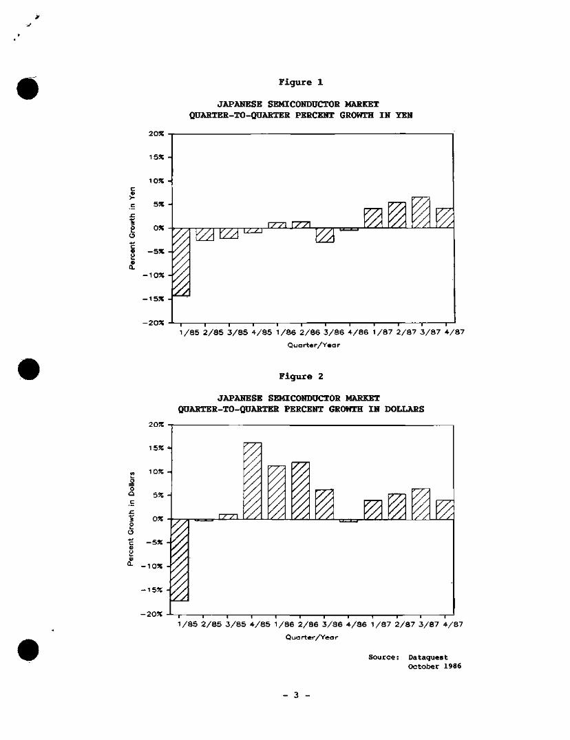
Figure 1
JAPANESE SEMICONDUCTOR MARKET QUARTER-TO-QUARTER PERCENT GROffTH IN YEN
20JK
-20?e -I 1 1 r—~n r 1 / 8 5 2 / 8 5 3 / 8 5 4 / 8 5 1 / 8 6 2 / 8 6 3 / 8 6 4 / 8 6 1 / 8 7 2 / 8 7 3 / 8 7 4 / 8 7
Quarter/Year
O a
I c V v a.
F i g u r e 2
JAPANESE SEMICONDUCTOR MARKET QUARTER-TO-QUARTER PERCENT GROWTH IN DOLLARS
2 0 %
15% -
10% -
- 5 %
- 1 0 %
• 1 5 % -
" 2 0 % — - 1 1 1 j 1 1 1 1 j 1 1 [-
1 / 8 5 2 / 8 5 3 / 8 5 4 / 8 5 1 / 8 6 2 / 8 6 3 / 8 6 4 / 8 6 1 / 8 7 2 / 8 7 3 / 8 7 4 / 8 7
Quarter/Year
Source: Dataquest October 1986
- 3
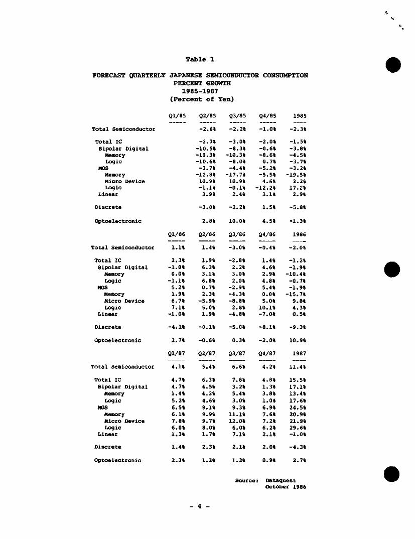
T a b l e 1
FORECAST QUARTERLY JAPANESE SEMICONDUCTOR CONSUMPTION P E R C E N T GROWTH
1 9 8 5 - 1 9 8 7 ( P e r c e n t o f Y e n )
Ql /85 Q2/85 Q3/85 Q4/85 1985
Total Seaiiconductor
Total IC Bipolar Digital Heaocy Logic
HOS Memory Micro Device Ijogic
Linear
-2.6%
-2.7% -10.5% -10.3% -10.6% -3.7% -12.8% 10.9% -1.1% 3.9%
-2.2%
-3.0% -8.3% -10.3% -8.0% -4.4%
-17.7% 10.9% -0.1% 2.4%
-1.0%
-2.0% -0.6% -8.6% 0.7%
-5.2% -5.5% 4.6%
-12.2% 3.1%
-2.3%
-1.5% -3.8% -4.5% -3.7% -3.2% -19.5% 2.2%
17.2% 2.9%
D i s c r e t e -3.8% -2.2% 1.5% -5.8%
( ^ t o e l e c t r o n i c 2.8% 10.0% 4.5% -1.3%
'otal Semiconductor
Total IC Bipolar Digital Memory Logic
MOS Hemacy Micro Device Logic
Linear
Discrete
Ql/86
1.1%
2.3% -1.0% 0.0%
-1.1% 5.2% 1.9% 6.7% 7.1%
-1.0%
-4.1%
Q2/86
1.4%
1.9% 6.3% 3.1% 6.8% 0.7% 2.3%
-5.9% 5.0% 1.9%
-0.1%
Q3/86
-3.0%
-2.8% 2.2% 3.0% 2.0%
-2.9% -4.3% -8.8% 2.8%
-4.8%
-5.0%
Q4/86
-0.4%
1.4% 4.6% 2.9% 4.8% 5.4% 0.0% 5.0%
10.1% -7.0%
-8.1%
1986
-2.0%
-1.2% -1.9%
-10.4% -0.7% -1.9%
-15.7% 9.8% 4.3% 0.5%
-9.3%
Optoelectronic
'otal Semiconductor
Total IC Bipolar Digital Memory Logic
HOS Memory Micro Device Logic
Linear
Discrete
2.7%
Ql/87
4.1%
4.7% 4.7% 1.4% 5.2% 6.5% 6.1% 7.8% 6.0% 1.39
1.4%
-0.6%
Q2/87
5.4%
6.3% 4.5% 4.2% 4.6% 9.1% 9.9% 9.7% 8.0% 1.7%
2.3%
0.3%
Q3/87
6.6%
7.8% 3.2% 5.4% 3.0% 9.3% 11.1% 12.0% 6.0% 7.1%
2.1%
-2.0%
Q4/87
4.2%
4.8% 1.3% 3.8% 1.0% 6.9% 7.6% 7.2% 6.2% 2.1%
2.0%
10.9%
1987
11.4%
15.5% 17.1% 13.4% 17.6% 24.5% 20.9% 21.9% 29.6% -1.0%
-4.3%
Optoelectronic 2.3% 1.3% 1.3% 0.9% 2.7%
Source : f te taques t October 1986
- 4 -
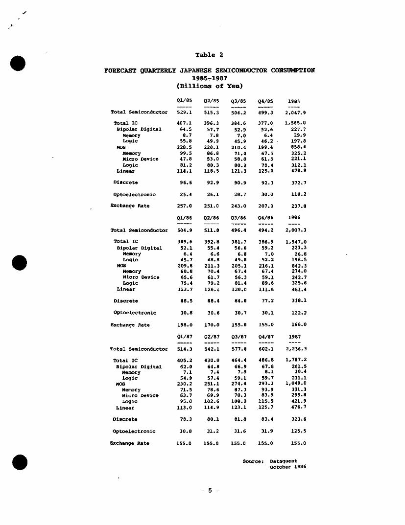
Table 2
FORECAST QUARTERLY JAPANESE SEMICONDUCTOR CONSUMPTION 1985-1987
(Billions of Yen)
Ql/85 Q2/85 Q3/85 Q4/85 1985
Total Semiconductor
Total IC Bipolar Digital Memory Logic
MOS Memory Micro Device Logic
Linear
Discrete
Optoelectronic
Exchange Rate
Total Semiconductor
Total IC Bipolar Digital Memory Logic
HOS Memory Micro Device Logic
Linear
Discrete
Optoelectronic
Exchange Rate
529.1
407.1 64.5 8.7 55.8
228.5 99.5 47.8 81.2
114.1
96.6
25.4
257.0
Ql/86
504.9
385.6 52.1 6.4
45.7 209.8 68.8 65.6 75.4 123.7
88.5
30.8
188.0
515.3
396.3 57.7 7.8
49.9 220.1 86.8 53.0 80.3
118.5
92.9
26.1
251.0
Q2/86
511.8
392.8 55.4 6.6
48.8 211.3 70.4 61.7 79.2 126.1
88.4
30.6
170.0
504.2
384.6 52.9 7.0 45.9 210.4 71.4 58.8 80.2 121.3
90.9
28.7
243.0
Q3/86
496.4
381.7 56.6 6.8
49.8 205.1 67.4 56.3 81.4 120.0
84.0
30.7
155.0
499.3
377.0 52.6 6.4 46.2 199.4 67.5 61.5 70.4 125.0
92.3
30.0
207.0
Q4/86
494.2
386.9 59.2 7.0
52.2 216.1 67.4 59.1 89.6 111.6
77.2
30.1
155.0
2,047.9
1,565.0 227.7 29.9 197.8 858.4 325.2 221.1 312.1 478.9
372.7
110.2
237.0
1986
2,007.3
1,547.0 223.3 26.8 196.5 842.3 274.0 242.7 325.6 481.4
338.1
122.2
166.0
Ql/87 Q2/87 Q3/87 Q4/87
Total Semiconductor 514.3 542.1 577.8 602.1
Total IC 405.2 430.8 Bipolar Digital 62.0 64.8 Memory 7.1 7.4 Logic 54.9 57.4
MOS 230.2 251.1 Memory 71.5 78.6 Micro Device 63.7 69.9 Logic 95.0 102.6
Linear 113.0 114.9
Discrete 78.3 80.1
Optoelectronic 30.8 31.2
Exchange Rate 155.0 155.0
464 66 7
59 274 87 78
108.8 123.1
486.8 67.8 8.
59. 293. 93. 83. 115. 125.
81.8
31.6
155.0
83.4
31.9
155.0
1987
2,236.3
1,787.2
261.5 30.4 231.1
1,049.0 331.3 295.8 421.9 476.7
323.6
125.5
155.0
Source: Oataquest October 1986
- 5
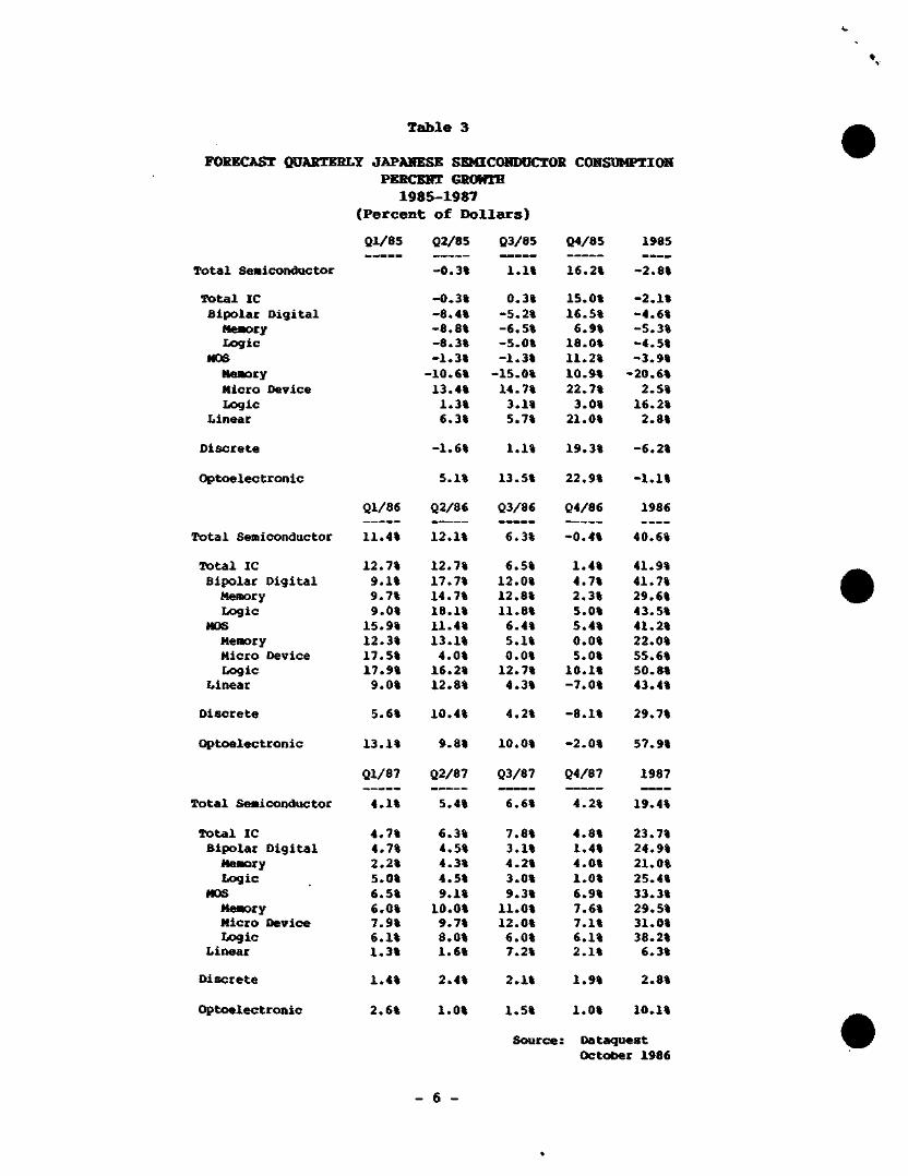
T a b l e 3
FORECAST (HIARTERL7 JAPANESE SEMICONIHICTOR CONSOMPTiaK PERCENT GROWTH
1 9 8 5 - 1 9 8 7 ( P e r c e n t o f I t o l l a r s )
T o t a l Semiconductor
r ro ta l IC B i p o l a r D i g i t a l
Henory Logic
MOS Henory Micro Device I«gic
Linear
Ql/85 Q2/85 Q3/85 Q4/85
-0.3% 1.1% 16.2%
1985
-2.8%
- 0 . 3 % -8.4% -8 .8% -8 .3% -1 .3% 10.6% 13.4%
1.3% 6.3%
0.3% -5 .2% -6 .5% -5.0% -1 .3%
-15.0% 14.7%
3.1% 5.7%
15.0% 16.5%
6.9% 18.0% 11.2% 10.9% 22.7%
3.0% 21.0%
- 2 . 1 % -4 .6% - 5 . 3 % -4 .5% -3 .9%
-20.6% 2.5%
16.2% 2.8%
Discrete -1.6% 1.1% 19.3% -6.2%
C^toelectronic
Total Semiconductor
Ql/86
11.4%
5.1%
Q2/86
12.1%
Discrete
Optoelectronic
Total Seaiconductor
5.6%
13.1%
Ql/87
4.1%
10.4%
9.8%
Q2/87
5.4%
13.5%
Q3/86
6.3%
Total IC 12.7% 12.7% 6.5% Bipolar Digital 9.1% 17.7% 12.0% Memory 9.7% 14.7% 12.8% Logic 9.0% 18.1% 11.8%
MOS 15.9% 11.4% 6.4% Memory 12.3% 13.1% 5. Micro Device 17.5% 4.0% 0. Logic 17.9% 16.2% 12.7%
Linear 9.0% 12.8% 4.3%
1% 0%
4.2%
10.0%
Q3/87
6.6%
22.9%
Q4/86
-0.4%
4% 7% 3% 0% 4% 0% 0%
10.1% -7.0%
-8.1%
-2.0%
Q4/87
4.2%
-1.1%
1986
40.6%
41.9% 41.7% 29.6% 43.5% 41.2% 22.0% 55.6% 50.8% 43.4%
29.7%
57.9%
1987
19.4%
Total IC 4.7% 6.3% 7.8% 4.8% 23.7% Bipolar Digital 4.7% 4.5% 3.1% 1.4% 24.9% Memory 2.2% 4.3% 4.2% 4.0% 21.0% Logic 5.0% 4.5% 3.0% 1.0% 25.4%
MOS 6.5% 9.1% 9.3% 6.9% 33.3% Memory 6.0% 10.0% 11.0% 7.6% 29.5% Micro Device 7.9% 9.7% 12.0% 7.1% 31.0% Logic 6.1% 8.0% 6.0% 6.1% 38.2%
Linear 1.3% 1.6% 7.2% 2.1% 6.3%
Discrete 1.4% 2.4% 2.1% 1.9% 2.8%
Optoelectronic 2.6% 1.0% 1.5% 1.0% 10.1%
S o u r c e : Oateiquest Octot>er 1986
- 6 -
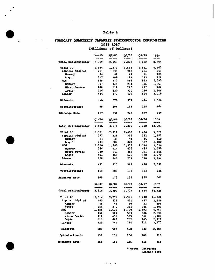
Table 4
FORECAST QUARTERLY JAPANESE SEMICONDUCTOR CONSUMPTION 1985-1987
(Millions of Dollars)
Total Semiconductor
Total IC Bipolar Digital Memory Logic
MOS Memory Micro Device Logic
Linear
Discrete
Optoelectronic
Exchange Rate
Total Semiconductor
Total IC Bipolar Digital Memory Logic
MOS Memory Micro Device Logic
Linear
Discrete
Optoelectronic
Exchange Rate
Total Semiconductor
Total IC Bipolar Digital Memory Logic
MOS Memory Micro Device Logic
Linear
Discrete
Optoelectronic
Exchange Rate
Q
2
1
1/85
,059
,584 251 34 217 889 387 186 316 444
376
99
257
Ql/86
2
2
1
,686
,051 277 34
243 ,116 366 349 401 658
471
164
188
Ql/87
3
2
1
,318
,614 400 46 354 ,485 461 411 613 729
505
199
155
Q2/85
2,053
1,579 230 31
199 877 346 211 320 472
370
104
251
Q2/86
3,011
2,311 326 39
287 1,243
414 363 466 742
520
180
170
Q2/87
3,497
2,779 418 48 370
1,620 507 451 662 741
517
201
155
Q3/85
2,075
1,583 218 29 189 866 294 242 330 499
374
118
243
Q3/86
3,202
2,462 365 44
321 1,323 435 363 525 774
542
198
155
Q3/87
3,727
2,995 431 50 381
1,770 563 505 702 794
528
204
155
Source
Q4/85
2,412
1,821 254 31 223 963 326 297 340 604
446
145
207
Q4/86
3,188
2,496 382 45
337 1,394 435 381 578 720
498
194
155
Q4/87
3,884
3,140 437 52
385 1,892
606 541 745 811
538
206
155
1985
8,599
6,567 953 125 828
3,595 1,353 936
1,306 2,019
1,566
466
237
1986
12,087
9,320 1,350
162 1,188 5,076 1,650 1,456 1,970 2,894
2,031
736
166
1987
14,426
11,528
1,686 196
1,490 6,767 2,137 1,908 2,722 3,075
2,088
810
155
: Dataquest October 1986
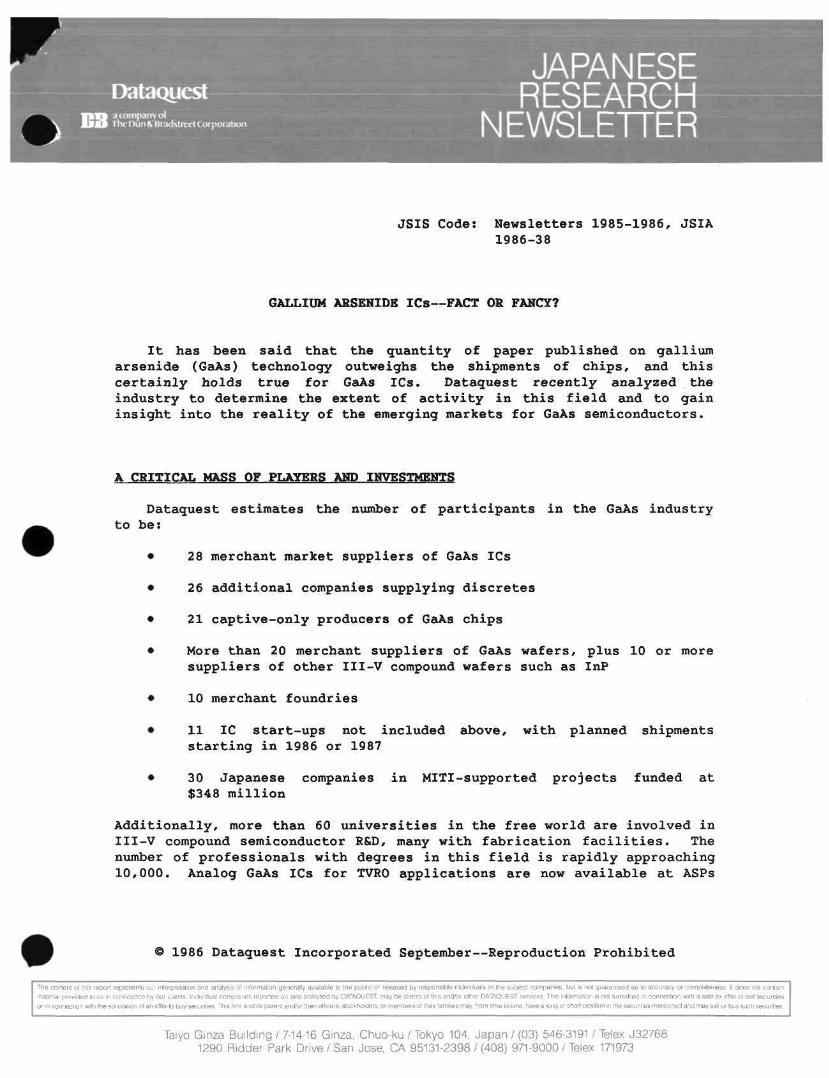
r DataQuest ^Koinpaiivur ThcDuittl'UraekltvrlCiMpwjIiun
JAPANESE RESEARCH
NEWSLETTER
JSIS Code: Newsletters 1985-1986, JSIA 1986-38
GALLIUM ARSENIDE ICs—FACT OR FANCY?
It has been said that the quantity of paper published on gallium arsenide (GaAs) technology outweighs the shipments of chips, and this certainly holds true for GaAs ICs. Dataguest recently analyzed the industry to determine the extent of activity in this field and to gain insight into the reality of the emerging markets for GaAs semiconductors.
A CRITICAL MASS OF PLAYERS AMD IMVESTMENTS
Dataguest estimates the number of participants in the GaAs industry to be:
28 merchant market suppliers of GaAs ICs
26 additional companies supplying discretes
21 captive-only producers of GaAs chips
More than 20 merchant suppliers of GaAs wafers, plus 10 or more suppliers of other III-V compound wafers such as InP
10 merchant foundries
11 IC start-ups not included above, with planned shipments starting in 1986 or 1987
30 Japanese companies in MITI-supported projects funded at $348 million
Additionally, more than 60 universities in the free world are involved in III-V compound semiconductor R&D, many with fabrication facilities. The number of professionals with degrees in this field is rapidly approaching 10,000. Analog GaAs ICs for TVRO applications are now available at ASPs
1986 Dataguest Incorporated September—Reproduction Prohibited
The conlenl of this report represents our inlerpretalion anid analysis ot information generally available to the public or released by responsible inidiviI:tuals in the sub|ect companies, but is not guaranteed as lo accuracy or completeness It does nol contain material provided to us in confidence by our clients Individual companies reported on and analyzed by DATAQUEST may be clients of this and/or other DATAQUfST services This information is nol furnished in connection with a sale or offer to sell securities or in conneclion with the solicitation otan offer to buy securities This firm and its parent and/or their officers, stockholders, or members of Iheir families may, from lime to lime, have a long or short position in the securilies mentioned and may sell or buy such securities
Taiyo Ginza Building / 7-14-16 Ginza, Chuo-ku / Tokyo 104, Japan / (03) 546-3191 / Telex J32768 1290 Ridder Park Drive / San Jose, CA 95131-2398 / (408) 971-9000 / Telex 171973
K of less than $20. Vitesse Electronics Corporation has announced a 2g00-type bit slice family of digital ICs that includes a lKx4 SRAM and are based on a 1.2|i E/D MESFET process. Dataquest estimates that capital i n f u s i o n into the GaAs IC field exceeded $330 m i l l i o n in 1985.
WHAT IS THE FOTURE OF THE GaAs IC INDUSTRY?
A recent Dataquest analysis of available high-speed ICs shows that silicon technology is evo lv ing rapidly on several fronts. CMOS processes are now pushing critical dimensions (CDs) to less than l.Sp. and, in some cases, below 1.0|i, resulting in subnanosecond gate delays. ECL gate arrays based on sub-u CDs are now in limited volume production and feature gate delays of less than 300 picoseconds. This progress, coupled with product schedule slippages at several major GaAs digital houses, has raised some doubt as to the viability of using GaAs digital ICs in new systems now being developed, especially at bottom-line-sensitive U.S. computer houses. This situation has also inspired many U.S.-based silicon IC suppliers to maintain the status quo of evolutionary progress in silicon as opposed to extending themselves by risking investment in GaAs.
Dataquest observed during this analysis that all of the Japanese GaAs IC suppliers are vertically integrated, supplying communications and EDP equipment; many also produce their own wafers. This contrasts sharply with the typical U.S. GaAs IC start-up, which is a "chips-only" company.
Despite the number of players in the GaAs arena, wafer defect densities are still excessive with respect to LSI chip fab requirements. This problem and the problem of gate threshold control have, to date, prevented the introduction of cost-effective GaAs chips into commercial systems. However, these problems are r e s o l v a b l e with the appropriate application of presently understood technology. The GaAs IC situation today is not unlike the Si NMOS situation in 1971, when the industry struggled t o produce the standard IK DRAM, the 1103. At that time. Burroughs, NCR, and others took leadership positions by designing the 1103 into systems and pressuring the U.S. industry to rise to the occasion, which it did. Today, to Dataquest's knowledge, only one U.S. systems house is applying similar pressure to potential GaAs RAM suppliers. If history is any indicator, the GaAs IC industry needs several more courageous champions within systems houses demanding tens of millions of GaAs LSI chips and backing their demands with purchase orders and multiyear schedules. It now appears that if such a situation evolves, it will do so in Japan, leading to a further demise of U.S. EDP houses in the world marketplace.
- 2 -
DATAOUEST CONCLUSIONS
While the U.S. Department of Defense appears to be pushing the U.S. industry very hard for viable merchant GaAs IC sourcing, many potential suppliers are limited by the lack of adequate additional demand from the commercial sector. This shortfall in demand is preventing a sufficiently rapid buildup of volume, making it difficult, if not impossible, to achieve the minimum efficiency of scale required for the success of the GaAs IC industry. The MITI-backed effort at vertically integrated Japanese firms does not face the same limitation; the net effect may be the eventual domination of the emerging worldwide GaAs IC market by Japanese firms. However, the race has just started, with only two Japanese suppliers of merchant GaAs ICs at present; a few courageous "drivers" in U.S. systems houses could have a major impact on the outcome.
Gene Miles
- 3 -
Dataquest 3 companv t?l 1W- l">un&-HradMiftltorporatum
JAPANESE RESEARCH
NEWSLETTER
JSIS Code: Newsletters 1985-1986, JSIA 1986-39
THE SMAST IC CARD—MARKET OVERVIEW
INTRODUCTION
By 1990 the total number of magnetic credit cards in circulation worldwide will top 1 billion. The credit card has become an accepted part of everyday life. Popular though it is, this card is no t without its limitations. Small memory capacity, a limited lifetime, and a susceptibility to fraud are factors limiting the true market potential for growth and acting as a driving force in bringing about the next generation of credit cards—the IC card.
IC CARD
The IC card, "smart card," or intelligent data carrier, as it is sometimes called, is a credit card with an integrated circuit imbedded in it. Metal contacts on the surface of the card allow the integrated circuit to be accessed by interfaced circuitry and the information held on the card to be updated. The International Standards Organization (ISO) has begun the process of creating standards for the IC card that will be used in financial transactions. Discussed below are the areas in which critical parameters are being specified.
Mechanical Stability
The IC card must be able to withstand the harsh environmental stresses to which a standard credit card is subjected. Some of the most rigorous torsional requirements experienced by the card take place during wintertime when the cards are pressed into service for clearing frosty windshields. The North American user subjects the credit cards to much greater wear and tear than his European or Asian counterpart. European and Asian males tend to carry their credit cards in their jacket pockets or in purses whereas North American males regularly sit upon theirs. All these factors have been taken into account in arriving at the current specification.
1986 Dataquest Incorporated September—Reproduction Prohibited
The content of this reprort represents our interpretation and analysis of information generally available to the public or released by responsible individuals in the subject companies but is not guaranteed as to accuracy or completeness It does not contain material provided to us in confidence by our clients Individual companies reported on and analyzed by DATAQUEST, may be clients of this and/or other DATAQUEST services This information is not furnished in connection with a sale or offer to sell securities or in connection with the solicitation of an offer to buy securities This firm and its parent and/or their officers, stockholders, or members of their families may, from time to time have a long or short position in the securities mentioned and may sell or buy such securities
Taiyo Ginza Building / 7-14-16 Ginza, Chuo-ku / Tokyo 104, Japan / (03) 546-3191 / Telex J32768 1290 Ridder Park Drive / San Jose, CA 95131-2398 / (408) 971-9000 / Telex 171973
Security
The device has to be secure, meaning that its c o n t e n t s should not be able to be read or modified by unauthorized persons. As part of the evaluation of the prospective vendors for their CP8 card, the French company CII Honeywell Bull used the services of the National Security Organization to determine how the cards could be accessed or tampered with. Tests included a scanning electron-microscope evaluation and microprobing of the die surface. Only one IC card out of the four under review passed all the security tests.
Elec t ron ic Protocols
Important for the acceptance of the card within the global financial community is the standardization of the electronic signals and exchange protocols used in reading and writing information to the card. At the time of writing, this specification is still being worked on by the major card manufacturers and financial institutions represented on the ISO.
Contact Location
ISO has agreed to adopt the CP8 French standard as the international smart card standard. This decision was reached in two stages. In May 1985, the United States withdrew its objections to the existence of two standards for the position of the chip on the card. The French chip is placed at the top of the card while other manufacturers have a chip at the bottom. ISO then accepted the French standard for the exchange of information. The technology, invented by the French inventor Roland Moreno, was adopted by Bull and thus has given Bull a substantial lead over other smart card manufacturers. Mr. Moreno has been in contact with a number of Japanese electronics groups, which could lead to the licensing of the French smart card technology in Japan.
THE MAGNETIC MARKET
North America is the premier credit card marketplace. Within this geographic area. Visa and MasterCard together have achieved 40 percent penetration of the marketplace while the upscale American Express Card has 15 percent. Further market development is limited by the increasing number of expensive on-line authorizations and the growth of fraud. Visa and MasterCard reported a combined fraud, abuse, and authorization cost of $902 million as of 1984, and estimate an additional cost of $21.5 billion by 1990. These factors, combined with the high potential for innovative intelligent new products afforded by a smart IC card, are generating the hotbed of activity surrounding IC card trials. The magnetic card is fighting back in the guise of the latest magnetic striped card under trial with Visa. This card uses magnetic stripes to increase memory capacity and the complexity of user validation, thereby increasing both the lifetime and the security quotient of the card.
TYPES OF IC CARDS
The IC card can be divided into two distinct types: a simple version containing only memory and a more complex form consisting of the processor core with an interface to memory.
Memory Card
EPROM, EEPROM, and fusible link-based technologies are under development, where 16K bits of memory correspond to 2,000 letters. The current cash card has a capacity of 0.6K bits of memory, or 75 letters. The increased availability of larger EPROMs and EEPROMs is an important factor in the growth of this sector, with 128K-bit and 256K-bit memories currently under development. Applications include usage as a robust storage medium for data that would normally be held on a magnetic tape or in a floppy disk format. In an industrial production environment it will be ideal as a batch tracking medium, processing information being modified and updated as production lots move from station to station.
Processor Card
Built-in processing power in the form of a CPU core interfacing with memory on a chip or as part of a two-chip set increases the flexibility and hence the niunber of applications available to the user. For example,
• The handling of multiple bank accounts
• The ability to deal with transactions in a variety of currencies
• Its use as a personal directory/memorandum
!» The use of a single card for many transactions (e.g., financial, educational, and social)
In addition, the more intelligent the card the higher the levels of security that can be implemented. Worldwide credit card fraud is presently estimated at more than $500 million per year.
Outlined below is a resume of the market situation by country. A list of IC card activity by region is detailed in Table 1.
France
In March 1985, France announced its intention to establish a sophisticated nationwide cashless retailing method involving an initial investment of FFr220 million. This scheme is based on the IC card and incorporates a two-stage introduction schedule. The first stage is the introduction of 3 million cards in four regions of France, namely
- 3 -
Brittany, Calais, Lyons, and the Riviera. The second stage of investment is scheduled to spread into 12 million smart cards around the whole country by the end of 1988. The total cost for both stages will be around FFrl billion. Concerted action has been planned by the Post Office and Savings Banks in France for IC cards. DGT, the French telecommunications authority, is to place an order for 1 million cards for coinless pay phones with 15,000 such booths in use by early 1987.
Though Bull of France and Olivetti of Italy have agreed to form a joint venture for the development and production of automatic teller machines (ATMs) the agreement would result in an ATM operation large enough to be competitive worldwide. TRT Telecommunications and Informatique, the French electronics company owned by Philips, have been awarded a FFr130 million contract to provide IC cards for the French banking payments network. The order was signed with the Carte Bancaire organization which will supply 4.2 million cards over the next three years. The Carte Bancaire organization also has a contract with Bull for 12.4 million cards to be shipped by 1988.
Italy
A trial system in Bormio, North Italy, has been using 5,000 IC cards and 35 terminals. This is being operated as a joint venture between Credito Valtellinese and Intelmatique, a subsidiary of the French PTT.
Japan
Although not as fast as their European counterparts at introducing IC card trials, Japanese manufacturers have nevertheless been moving quickly to strengthen their position in the domestic market. The test results are being used to lobby U.S. companies with a view to making inroads into the important North American marketplace. There have been a number of trials running during 1985 and 1986. One of the most notable is between the Siunitomo Bank and Kyowa Bank in Haikarigaoka Park Town, Mitaka City. This was a financial system, with the card being utilized for banking, home shopping, and cable television (CATV) charge accounts. In Tokyo, The Women's University of Medicine has developed a health control card system called Sante. It uses an electronic module that accepts input data on the patient's health history.
The manufacturing and assembly process for IC cards has to be controlled within very fine limits. IC card manufacture lends itself well to the assembly, production and electronic techniques developed by the watch and calculator manufacturers. Dataquest believes that, given the opportunity, Japan has the technological infrastructure to capitalize quickly on the global market opportunity presented by the IC card.
- 4 -
United Kingdom
Thorn EMI has plans to supply smart cards fo r an identification system developed to help solve soccer hooliganism. Sperry would supply the computer terminals. British Telecom is looking to increase the use of prepaid phone cards for its pay phones, and an IC card is one system under consideration. Another use for smart cards is demonstrated by Paytel, a cable TV company, which makes pay-per-view television equipment operated by debit cards.
United States
MasterCard started two IC card tests, one in Washington, D.C., using Bull cards and one in Florida using Casio cards. For each of these two tests MasterCard has made 50,000 cards available. MasterCard's version uses an intelligent terminal to debit the balance held in the card. This requires dual ownership, i.e., acceptance by the terminal and knowledge by the person holding the card of the authorization code, before the transaction will be completed. Bull, anticipating a favorable outcome of its trials against Casio, is pressing ahead to begin production of smart cards in the fall at a new facility in Dallas, Texas.
MasterCard's major rival. Visa, has recently unveiled plans for a super IC card incorporating a touch-sensitive keyboard and display which it expects to test in about 18 months. This card will eliminate the need for special terminals. The card carries account balances that are created as the card is loaded with deposits by punching in a code provided by the bank. After each purchase, the balance on the Visa card is debited by the amount used. If the cardholder tries to make a purchase for more than the amount the card contains, he or she will not receive an authorization code.
West Germany
A banking committee has been formed, headed by the Deutsche Sparekassen and the Giroverband, to implement an IC card scheme. The banks believe this will complement the Eurocheque guarantee cards currently held by 50 percent of their banking customers.
Sheridan Tatsuno Jennifer Berg
- 5 -
Table 1
IC CARD ACTIVITY BY GEOGRAPHIC REGION
Location
Australia
Canberra
Canberra
Perth
Sydney
Company
Commonwealth Bank
The National Bank
ANZ
NSW State Bank
Activity
Bank trial with Steria (France)
Bank trial with Steria (France)
Bank trial with Steria (France)
Bank trial with Steria (France)
Canada
Toronto Royal Bank of Canada Use of Bull IC card as an access security device to financial network
France
Aix--en-Provence
Grenoble
Paris
Paris
Paris
Paris
Paris
Paris
Trappes
Thomson
Crouzet
Carte Bancaire
Credit Agricole
Credit Mutuel
DGT (French PTT)
Sch1umberger
Steria
Bull
IC manufacture for Bull
IC card electronic cash registers
Installing IC card payment network
MasterCard trial
MasterCard trial
15,000 telephone paybooths by the end of 1986
IC card manufacturer
Card designer
IC card manufacturer
(Continued)
- 6 -
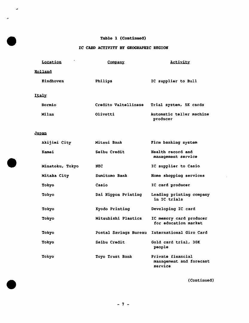
Table 1 (Continued)
IC CARD ACTIVITY BY GEOGRAPHIC REGION
Location
Holland
Eindhoven
Company
Philips
Activity
IC supplier to Bull
Italy
Bormio
Milan
Credito Valtellinese Trial system, 5K cards
Olivetti Automatic teller machine producer
Japan
Akijimi C
Kamei
Minatoku,
Mitaka Ci
Tokyo
Tokyo
Tokyo
Tokyo
Tokyo
Tokyo
ity
Tokyo
ty
Mitsui Bank
Seibu Credit
NEC
Sumitomo Bank
Casio
Dai Nippon Printing
Kyodo Printing
Mitsubishi Plastics
Postal Savings Bure;
Seibu Credit
Tokyo Toyo Trust Bank
Firm banking system
Health record and management service
IC supplier to Casio
Home shopping services
IC card producer
Leading printing company in IC trials
Developing IC card
IC memory card producer for education market
International Giro Card
Gold card trial, 30K people
Private financial management and forecast service
(Continued)
- 7 -
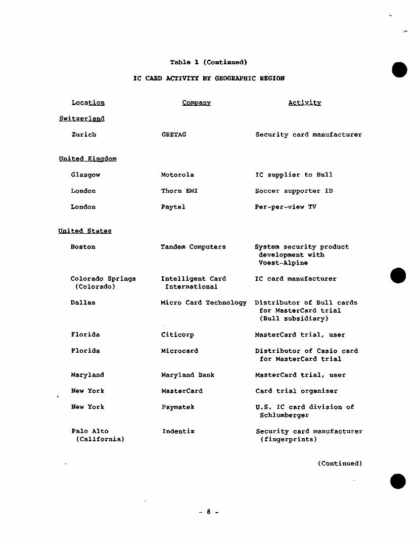
Table 1 (Cont inued)
IG CARD ACTIVITY BY GEOGRAPHIC REGION
Location
Switzerland
Zurich
Company
GRETAG
Activity
Security card manufacturer
United Kingdom
Glasgow
London
London
Motorola
Thorn EMI
Paytel
IC supplier to Bull
Soccer supporter ID
Per-per-view TV
United States
Boston
Colorado Springs (Colorado)
Dallas
Florida
Florida
Maryland
New York
New York
Palo Alto (California)
Tandem Computers
Intelligent Card International
Micro Card Technology
Citicorp
Microcard
Maryland Bank
MasterCard
Paymatek
Indentix
System security product development with Voest-Alpine
IC card manufacturer
Distributor of Bull cards for MasterCard trial (Bull subsidiary)
MasterCard trial, user
Distributor of Casio card for MasterCard trial
MasterCard trial, user
Card trial organizer
U.S. IC card division of Schlumberger
Security card manufacturer (fingerprints)
(Continued)
- 8
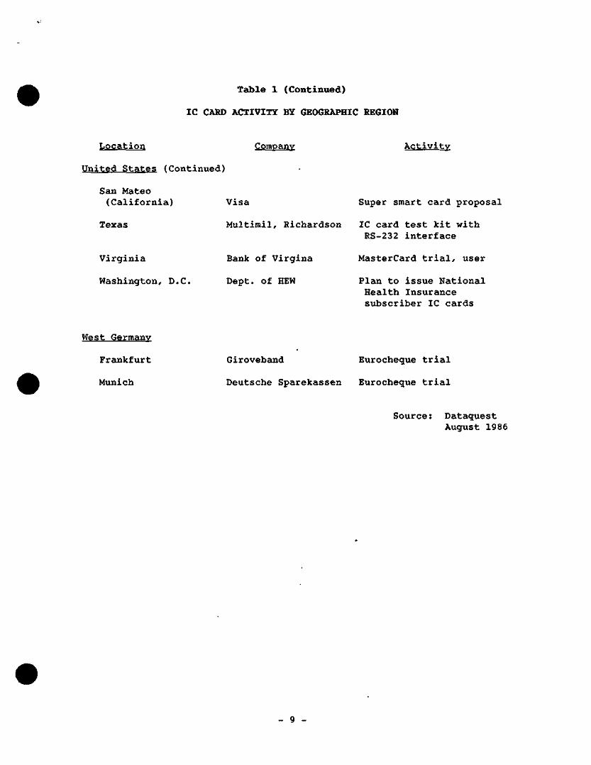
Table 1 (Continued)
IC CARD ACTIVITY BY GEOGRAPHIC REGION
Location
United States (Continued)
San Mateo (California)
Company Activity
Texas
Virginia
Washington, D.C.
Visa
Multimil, Richardson
Bank of Virgina
Dept. of HEW
Super smart card proposal
IC card test kit with RS-232 interface
MasterCard trial, user
Plan to issue National Health Insurance subscriber IC cards
West Germany
Frankfurt
Munich
Giroveband Eurocheque trial
Deutsche Sparekassen Eurocheque trial
Source: Dataquest August 1986
Dataquest MMMB Ttw nunSTBi^dstrccKorporation
JAPANESE RESEARCH
NEWSLETTER
JSIS Code: Newsletters 1985-1985, JSIA 1986-40
AMD'S ANNUAL SHAREHOLDERS' MEETING
INTRODUCTION
Advanced Micro Devices' (AMD) annual shareholders' meeting, originally scheduled to take place on September 10 at the Pierre Hotel in New York, was relocated to AMD's office building in the Lawrence Business Park on Lawrence Expressway in Sunnyvale, California. As AMD President and CEO Jerry Sanders set the scene for the semiconductor industry in the United States, it became apparent why the change had occurred—economic pressures. U.S. semiconductor manufacturers' combined losses were approximately $500 million in 1985 and AMD's fiscal year 1986 was the worst in its history. On sales of $576 million in fiscal year 1986, AMD lost $37 million or 65 cents a share. This compares to 1985 earnings of $135 million on sales of $931 million. Revenue for the first two quarters of 1986 was essentially flat at $153 million and $154 million, respectively, with losses of $11 million and $28 million, respectively.
To the question, "Is it too late to save the U.S. semiconductor industry?" Mr. Sanders responds with a firm "No!" How can U.S. semiconductor manufacturers compete in a global market? Innovation, he believes, is the key. In 1986, AMD invested $184 million or 32 percent of sales in R&D and it has spent about 25 percent of total sales on capital investment over the last five years. However, now that excess capacity has reduced the need for capital spending, AMD is now spending at only half of last year's level.
AMD's stated goals are to maintain its RS.D expenditure and its commitment to the employees. Although the semiconductor industry is cyclical in nature, which accounts somewhat for the depressed state of the industry, the realities of the marketplace have changed. Fierce international competition and predatory pricing, the overall weak economy and underutilized capacity, and AMD's oversized (in the circumstances) infrastructure and no lay-off policy, have resulted in the worst financial year yet in AMD's history.
1986 Dataquest Incorporated September—Reproduction Prohibited
The content of this report represents our interpretation and analysis of information generally available lo the public or released by responsible individuals in ihe subject companies, but is not guaranteed as lo accuracy or completeness It does not contain material provided 'o us m confidence by our clients Individual companies reported on and analyzed by DATAQUEST, may be clients of this and/or other DATAQUEST services This information is not furnished in connection with a sale or offer to sell securities or in connection with the solicitation of an offer to buy securities This firm and its parent and/or their officers, stocl<holders, or members of ttieir families may, from lime to time riave a long or short position m the securities mentioned and may sell or buy such securities
Taiyo Ginza Building / 7-14-16 Ginza, Chuo-ku / Tokyo 104, Japan / (03) 546-3191 / Telex J32768 1290 Ridder Park Drive / San Jose, CA 95131-2398 / (408) 971-9000 / Telex 171973
AMD'S STRATEGY
To combat this turn of events, Mr. Sanders outlined AMD's three-part Strategy:
• To maintain competitive process technology
• To narrow the cost differential by more efficient manufacturing—a difficult task in today's economy
*; To bring innovative new products to market
Process Technology
EPROMs are AMD's technology driver for its process technology. In the fourth quarter of fiscal year 1985, EPROMs accounted for 23 percent of AMD's sales but declined to a low point in third quarter fiscal year 1986 to represent 65 percent of the company's operating losses. Largely due to predatory pricing by foreign suppliers that gained market share in the United States at the expense of domestic suppliers, ASPs for EPROMs declined sharply. Thus, because of the significance of EPROM technology to AMD's long-term well-being, AMD joined with other semiconductor manufacturers in the dumping suit brought against the Japanese in late 1985. Mr. Sanders sees the July 30, 1986, trade agreement as a big step forward to restoring equity to the marketplace, and is heartened by the U.S. government's recognition of the strategic importance of semiconductor technology to the economic health and defense of this country. The trade agreement, Mr. Sanders feels, could herald a new era of "constructive competition" and, if faithfully implemented, could offer a tremendous opportunity to U.S. semiconductor suppliers.
Economy
The current economic environment outlook is poor—the GNP is stagnant, factory utilization is down, ever more U.S. manufacturing is migrating off-shore, and the trade deficit is up, none of which augurs well for the near future. Faced with these conditions, AMD's response has been to drop marginal products, such as DRAMs—which represented less than 1 percent of sales in fiscal 1986, but caused considerable losses—and to increase factory utilization and lower manufacturing costs at its 6-inch wafer fab installation in Austin, Texas. In 1986, 72 percent of AMD's wafer starts were 5-inch and above, as compared to 1984 when 87 percent of wafers used were 4-inch and below. Along with the elimination of marginal products, the Company decided to revoke its "no lay-off policy" in August of this year, a decision which caused Mr. Sanders considerable pain and personal regret but which he recognized as necessary to provide the greatest good for the greatest number. Project reviews are now in progress to discuss which marginal projects should be eliminated, which may result in layoffs in October.
2 -
w TnTir>vat;if^Ti
RStD spending has been extremely high as a percent of sales and AMD's goal is to reduce it to around $40 million per quarter and to better focus it to leverage spending. The Liberty Chip program (one major new product a week starting in October 1985 through September 1986) has been successful, with 62 new product introductions to date, of which 22 are in CMOS. The most recent introduction was the 8895 hard disk controller. The newest member of the Liberty drive is the Am 29337 Bounds Checker, which deals with placement of data in memory. This product was introduced September 15.
DATAOUEST COMMENTS
The following issues were addressed during the question and answer portion of the meeting:
» AMD is the fourth largest foreign supplier to the Japanese market.
• AMD employment in Japan, now at 50 employees, will double in the near future.
* It was recently announced that the company will open a quality and reliability center, and next year a new sales office in Japan.
* Last quarter. Liberty sales accounted for 6 percent of sales and is growing.
* AMD is targeting early 1987 for renewed profitability, but this depends on many things, including getting costs in line and the actual product mix.
• Mr. Sanders is optimistic about the economy, but considers any further prognostication as too speculative.
* The company's largest customers are ordering more but distributor sales are down.
• AMD has just had its first successful run of a CMOS SRAM using 6-inch wafers.
• The 1Mb EPROM is in CMOS and many more products will be in CMOS.
• By and large, customer-specific ICs will not figure heavily in AMD's product portfolio, although where an opportunity exists to increase revenue in a unique way such an opportunity will be examined—for example, the decision to produce ECL gate arrays.
• Mr. Sanders considers AMD's proprietary chips to be "ASIC" (as opposed to CSIC, customer-specific ICs, such as gate arrays) and the company will continue to participate in the programmable products market with microprocessors, PROMs, and FPLDs.
- 3 -
• AMD's long- term product strategy is reflected in its linkup with Sony, undertaken with a view to defining new products for the consumer market segment where AMD has little experience.
• Investment is being made in ISDN products now, although the market may not be important until the 1988 through 1989 time frame.
• Mr. Sanders is not optimistic about acquiring second-source rights to Intel's 80386, at least in the near term, primarily because Intel is capable of supplying the market demands itself.
• AMD's strength lies partially in the diversity and breadth of its product offerings—no single product represents more than 10 percent of sales.
The new tax law tends t o be more punitive to capital-intensive business and the expectation is that it will increase AMD's tax liability over the next several years, although Mr. Sanders wryly commented that he was "looking forward to paying taxes." AMD's cash flow has been positive during the first half of 1986, and the company has no plans to go for bond or equity financing. The outlook for 1987 calls for a modest economic recovery and increased access to the Japanese market, but continuing concern over the worldwide glut. Conditions today are very different from the "good old days of" 1984, and only the "gold medalists" will survive.
Patricia S. Cox Patricia Galligan Janet Oncel
- 4
Dataquest .1 conipanv a\ The Dun &• Brad^t ictt CorpoRi tIon
RESEARCH BULLETIN
JSIS Code: Newsletters 1985-1986, JSIA 1986-41
ENTERING THE JAPANESE MARKET: NMB SEMICONDUCTOR AND NATIONAL SIGN FOUNDRY AGREEMENT
St3MMARY
NMB Semiconductor and National Semiconductor recently signed a long-term agreement to design, produce, and sell CMOS SRAMs in Japan. The initial agreement covers only 2Kx8 CMOS SRAMs but will be expanded to include three other configurations.
NMB Semiconductor currently produces CMOS DRAMs for Vitelic and Inmos and CMOS SRAMs for two undisclosed U.S. companies at its highly automated fab in Tateyama City, Chiba Prefecture. Completed in April 1985, the fab has two modules with 100 x 36-meter clean rooms, of which about 25 percent is Class 1 area. Module 1, which has a capacity of 20,000 to 24,000 wafers per month, handles 5-inch wafers. Module 2 handles 6-inch wafers. All wafer handling in the modules is fully automated.
DATAQUEST ANALYSIS
We believe that this agreement is significant for several reasons. Not only does it enable National to become a player in the Japanese SRAM market, but it helps NMB utilize its existing fab capacity. Moreover, it signals the growing use of Japanese foundries by major U.S. semiconductor makers. As shown in Table 1, many U.S. start-ups are already using Japanese foundries. Now major U.S. vendors are using Japanese foundries as a way to enter the Japanese market without having to make heavy capital investments up front. We see several emerging trends that will dramatically impact the semiconductor industry:
• More alliances between U.S. vendors and second-tier Japanese foundries to compete against the top 10 Japanese vendors
• The potential for major Japanese vendors to provide foundry to U.S. vendors to increase their capacity utilization, thereby lowering their fair market value for DRAMs and EPROMs (e.g., the recent Toshiba/Motorola DRAM agreement)
1986 Dataquest Incorporated September—Reproduction Prohibited
The content of Ihis repor". represents our interpretation and anaiys.s of nformanon generally available to Ihe pubc or released by responsible individuals m the sub]ecl companies but is not guaranteed as to accuracy or completeness It does nol contain
material provided lo us m confidence by our clients i-^d'V'duai companies reported on and analyzed by afiiTAOUEST may be clients of this and/or other DATAQUEST services This information is nol furnished in connecliori with a sale or oflet lo seil Securities
or in connection with the sdiotaiion ol an otter to buy securities This firm and its parent and/or their otiicers stockholders or members of their farriihes may, Irom nme to time nave a long or short pos'ton in Ihe securities mentioned and may s^l or buy such securities
Dataquest Incorporated, 1290 Ridder Park Drive, San Jose, CA 95131-2398, (408) 971-9000, Telex 171973
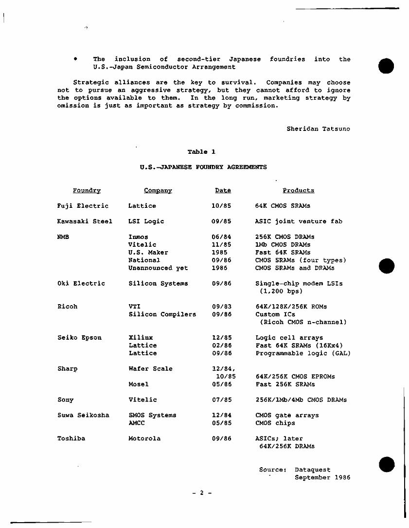
• The inclusion of second-tier Japanese foundries into the U.S.-Japan Semiconductor Arrangement
Strategic alliances are the key to survival. Companies may choose not to pursue an aggressive strategy, but they cannot afford to ignore the options available to them. In the long run, marketing strategy by omission is just as important as strategy by commission.
Sheridan Tatsuno
Table 1
U.S.-JAPANESE FGTJMDRY AGREEMENTS
Foundry
Fuji Electric
Kawasaki Steel
NMB
Company
Lattice
LSI Logic
Inmos Vitelic U.S. Maker National Unannounced yet
Date
10/85
09/85
06/84 11/85 1985 09/86 1986
Oki Electric Silicon Systems 09/86
Ricoh
Seiko Ep
Sharp
Sony
Suwa Sei
Toshiba
son
kosha
VTI Silicon Compilers
Xilinx Lattice Lattice
Wafer Scale
Mosel
Vitelic
SMOS Systems AMCC
Motorola
09/83 09/86
12/85 02/86 09/86
12/84, 10/85 05/86
07/85
12/84 05/85
09/86
Products
54K CMOS SRAMs
ASIC joint venture fab
256K CMOS DRAMs 1Mb CMOS DRAMs Fast 64K SRAMs CMOS SRAMs (four types) CMOS SRAMs and DRAMs
Single-chip modem LSIs (1,200 bps)
64K/128K/256K ROMs Custom ICs (Ricoh CMOS n-channel)
Logic cell arrays Fast 64K SRAMs (16Kx4) Programmable logic (GAL)
64K/256K CMOS EPROMs Fast 256K SRAMs
256K/lMb/4Mb CMOS DRAMs
CMOS gate arrays CMOS chips
ASICs; later 64K/256K DRAMs
Source: Dataguest September 1986
- 2 -
DataQuest TtH:t>un& (ttsditivcl CorpocslIon
RESEARCH BULLETIN
JSIS Code: Newsletters 1985-1986, JSIA 1986-37
EXAR HOLDS FIRST ANNUAL SHAREHOLDERS' MEETING
INTRODUCTION
Exar Corporation, the first Japanese subsidiary in Silicon Valley, held its first annual shareholders' meeting September 15, 1986, in San Jose, California. The meeting marked the beginning of Exar's life as a public company.
Exar, a Rohm Co., Ltd., subsidiary, was formed in 1971 as a joint venture between Rohm and three former Signetics engineers. Exar was the first Japanese-owned company to begin semiconductor fabrication in the United States', at its Sunnyvale, California, fab. In August 1985, Exar completed its initial public offering of stock, selling 1.4 million shares at $11 a share. In February 1986, .Exar acquired Exel Microelectronics Inc., a San Jose, California, manufacturer of EEPROMs. (Currently, Exar's stock is selling for $8.25 per share.)
MEETING HIGHLIGHTS
Exar's target application markets—telecommunications, data communications, computer peripherals, and industrial control and instrumentation—continue to provide strong growth opportunities for the company.
Exar's sales growth exceeded 100 percent from 1983 through 1986, although it dipped slightly in 1986, from $56.9 million to $52.5 million. The company has remained profitable, with net income of $4.4 million in fiscal 1986. Its parent company, Rohm Co., Ltd., accounted for 37.6 percent of Exar's total sales in fiscal 1986. Other international sales accounted for 17.0 percent of sales, and U.S. sales were 45.4 percent of sales.
© 1986 Dataquest Incorporated September—Reproduction Prohibited
The conient o( thIs reporl represents our mlerpteiation and analysis ol mformaiion generally available lo ihe public or released by responsit)le individuals m Ihe subjecl companies bul is nol guaranteed as to accuracy or completeness It does not contain
material orovided lo us in confidence Pv our clients Individual companies reponed on and analyzed by WTAOUEST may be clients of this and/or other DATAOUEST services This information is nol furnished m connection with a sale or ofler to sell securities
or m connection with the sdidiation d an ofter to buy securities This firm ana as pareni and/or iheir officers stockholdefs or members ol their families may. from time ID lime have a long or shon position in tt e secunties menlioned and may sell or buy such secunlies
Dataquest Incorporated, 1290 Ridder Park Drive, San Jose, CA 95131-2398, (408) 971-9000, Telex 171973
Along product lines, sales of linear/digital and digital ICs—the newer products—increased, while sales of the company's more mature linear ICs fell. In fiscal 1985, custom and standard product sales were almost equal; in fiscal 1986, custom product sales were much higher.
Exar's R&D expenditures increased to 10 percent of sales in fiscal 1986 ($5.3 million). Included in this figure was a VAX 8600 host computer for the engineering department.
The purchase of Exel Microelectronics has given Exar an inexpensive fab with Class 10 clean room and access to Exel's 2-micron CMOS and EEPROM technology. In addition, Exel's $40 million in operating losses and $3 million in tax credits give Exar tax benefits. Exar has restarted the Exel fab, and is continuing product development at Exel.
Exar's future plans include the offering of wafer foundry services, the development of analog/digital compilers jointly with Silicon Compilers, Inc., and a comprehensive USIC (User-Specific Integrated Circuit) program. In an effort to expand its international presence, Exar recently opened a design center in London.
NEW PRODUCTS
Two major new products have been developed by Exar and Exel, respectively. They are as follows:
• Exar's FLEXAR"^^: A flexible linear array that allows a designer to make any transistor in the array either NPN or PNP. In addition, unused bonding pads may be converted to resistors, capacitors, or diodes, as required.
• Exel's ERASIC^^: An electrically erasable programmable logic device (EEPLD) that allows multilevel logic.
Exel will soon introduce a 1-transistor cell EEPROM that the company believes will finally make EEPROMs competitive with EPROMs.
DATAOUEST COMMENTS
Exar has established a fine record as a profitable manufacturer of custom and standard linear, linear/digital, and digital ICs. The company has positioned itself well in a growing market. With majority ownership still in the hands of Rohm Co., Ltd., Exar has the ability and opportunity to continue to be both profitable and innovative.
Patricia S. Cox
Dataquesl ucorTip^nym Ihcnitn&RriKtsTricKc
JAPANESE RESEARCH
NEWSLETTER
JSIS Code: Newsletters 1985-1986, JSIA 1986-36
DATAQUEST ANNOUNCES FINAL 1985 JAPANESE SEMICONDUCTOR MARKET SHARE FIGURES
SUMMARY
This newsletter summarizes the data contained in the Market Share chapter of JSIS Volume I, Markets. The tables in this newsletter rank companies by product for 1984 and 1985. You may wish to file this newsletter behind the Market Share tab of JSIS Volume I.
WORLDWIDE SEMICONDUCTOR MARKET
In a worldwide semiconductor market that fell 16 percent in 1985, Japanese companies' revenues declined only 12 percent, due to their dominant position in their home market, which declined far less than the worldwide market.
NEC, with total worldwide semiconductor revenue of almost $2 billion, became the number one semiconductor supplier worldwide in 1985, the first year a Japanese company has held that position. Five of the top ten manufacturers in the world were Japanese companies in 1985, and Japanese companies gained worldwide market share, growing from 39.5 percent of the market in 1984 to 41.2 percent in 1985. The top five Japanese companies alone accounted for 28.7 percent of the total worldwide semiconductor market in 1985. The Japanese presence is most strongly felt in MOS memory and optoelectronics, areas in which they hold worldwide market shares of 56.9 percent and 50.0 percent, respectively.
Tables 1 through 12 give Japanese companies' 1984 and 1985 worldwide rankings in the major semiconductor product families.
1986 Dataquest Incorporated September—Reproduction Prohibited
The content of this report represents our interpretation and analysis of information generally avattable lo the public or released by responsible individuals in the subject companies, but is not guaranteed as lo accuracy or completeness It does not contain material provided to us in confidence by our clients Individual companies reported on and analyzed by DATAQUEST, may be clients of this and/or other DATAQUEST services This information is not furnished in connection with a sale or offer to sell securities Of in conr)ec(ion with the solicitation of an offer to buy securities This firm and its parent and/or their officers, stockholders, or members of their families may, from time to lime, have a long or short position in the securities mentioned and may sell or buy such securities
Taiyo Ginza Building / 7-14-16 Ginza, Chuo-ku / Tokyo 104, Japan / (03) 546-3191 / Telex J32768 1290 Ridder Park Drive / San Jose, CA 95131-2398 / (408) 971-9000 / Telex 171973
Table 1
WORLDWIDE SEMICONDUCTOR MARKET TOTAL SEMICONDUCTOR MARKET SHARE ESTIMATES
SALES BY JAPANESE MANUFACTURERS (Millions of Dollars)
Ranking Worldwide
1984 1985
1 2 3 4 6 5 7 9 8 10 12 11 13 14
Company
1 NEC 2 Hitachi 3 Toshiba 4 Fujitsu 5 Matsushita 6 Mitsubishi 7 Sanyo 8 Sharp 9 Oki 10 Rohm 11 Fuji Electric 12 Sony 13 Sanken 14 Seiko Epson
Other Japanese Companies
Japanese Companies
Total Market
1984
2,251 2,051 1,561 1,190
928 964 455 354 362 252 176 177 162 115
484
11,482
29,051
1985
1,984 1,671 1,459 1,020
906 706 457 329 307 250 173 168 149 93
438
10,110
24,543
Percent Change
1984-1985
-12% -19%
-1% -14% -2%
-27% 0%
-7% -15% -1% -2% -5% -8%
-19%
-10%
-12%
-16%
Source: Dataguest September 1986
- 2
Table 2
WORLDWIDE SEMICONDUCTOR MARKET TOTAL INTEGRATED CIRCUIT MARKET SHARE ESTIMATES
SALES BY JAPANESE MANUFACTURERS (Millions of Dollars)
Rank: ing Worldwide
1984
1 2 4 3 6 5 8 7 9
10 12 11 13 14
1985
1 2 3 4 5 6 7 8 9
10 11 12 13 14
Company
NEC Hitachi Toshiba Fujitsu Matsushita Mitsubishi Sanyo Oki Sharp Sony Rohm Seiko Epson Sanken Fuji Electric
Other Japanese Companies
Japanese Companies
Total Market
1984
1,838 1,569 1,035 1,098
592 766 305 343 238 132 111 115 47 32
307
8,528
2,788
1 1
7
18
1985
,603 ,236 995 940 595 510 314 289 201 130 105 93 46 31
299
,387
,706
Percent Change
1984-1985
-13% -21% -4%
-14% 1%
-33% 3%
-16% -16% -2% -5%
-19% -2% -3%
-3%
-13%
-18%
Source: Dataguest September 1986
Table 3
WORLDWIDE SEMICONDUCTOR MARKET TOTAL BIPOLAR DIGITAL MARKET SHARE ESTIMATES
SALES BY JAPANESE MANUFACTURERS (Millions of Dollars)
Rank: ing Worldwide
1984
1 2 3 4 5 6 7 8 9
10 11
1985
1 2 3 4 5 6 7 8 9
10 11
Company
Fujitsu Hitachi NEC Mitsubishi Toshiba Oki Matsushita Sanyo Rohm Sony Fuji Electric
Other Japanese Companies
Japanese Companies
Total Market
1984
305 223 134 123 37 25 22 18 15 8 2
32
944
4,778
1985
267 194 129 79 33 22 21 18 15 5 1
21
805
3,763
Source:
Percent Change
1984-1985
-12% -13%
-i% -36% -11% -12% -5% 0% 0%
-38% -50%
-34%
-15%
-21%
Dataquest September 1986
- 4 -
Table 4
WORLDWIDE SEMICONDUCTOR MARKET BIPOLAR DIGITAL MEMORY MARKET SHARE ESTIMATES
SALES BY JAPANESE MANUFACTURERS (Millions of Dollars}
Ranking Worldwide
1984 1985 Company
1 1 Fujitsu 2 2 Hitachi 3 3 NEC
Other Japanese Companies
Japanese Companies
Total Market
N/A = Not Applicable
984
136 59 23
0
218
807
1985
125 54 25
0
204
666
Percent Change
1984-1985
-8% -8%
9%
N/A
-6"%
-17"%,
Source: Dataquest September 1986
- 5
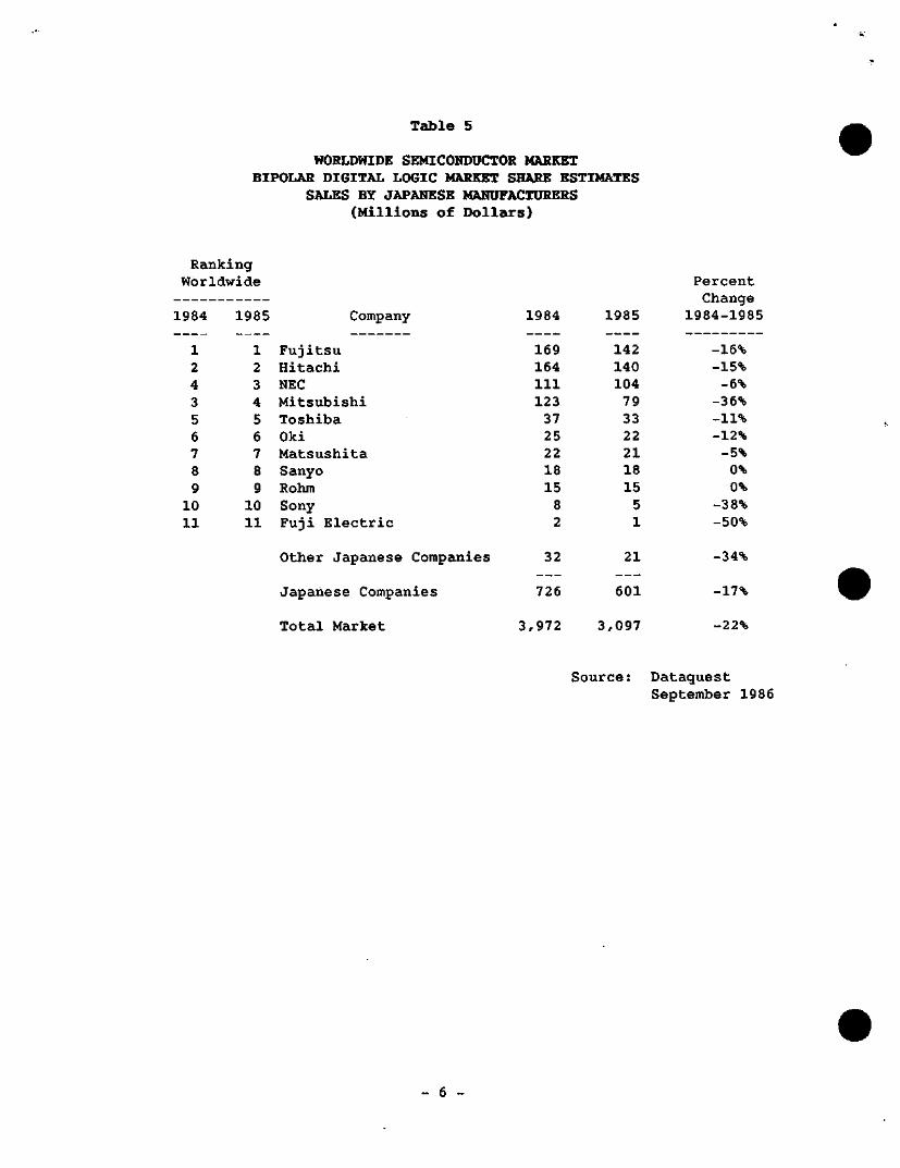
Table 5
WORLDWIDE SEMICONDUCTOR MARKET BIPOLAR DIGITAL LOGIC MARKET SHARE ESTIMATES
SALES BY JAPANESE MANUFACTURERS (Millions of Dollars)
Rank: Lng Worldwide
1984
1 2 4 3 5 6 7 8 9
10 11
1985
1 2 3 4 5 6 7 8 9
10 11
Company
Fujitsu Hitachi NEC Mitsubishi Toshiba Oki Matsushita Sanyo Rohm Sony Fuji Electric
Other Japanese Companies
Japanese Companies
Total Market
1984
169 164 111 123 37 25 22 18 15 8 2
32
726
3,972
1985
142 140 104 79 33 22 21 18 15 5 1
21
601
3,097
Source:
Percent Change
1984-1985
-16% -15% -6%
-36% -11% -12% -5% 0% 0%
-38% -50%
-34%
-17%
-22%
Dataquest September 1986
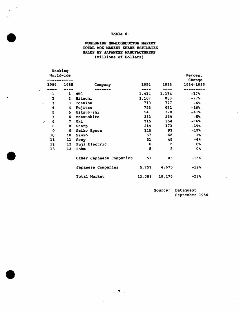
Table 6
WORLDWIDE S^ICONDUCTOR MARKET TOTAL MOS MARKET SHARE ESTIMATES SALES BY JAPANESE MANUFACTURERS
(Millions of Dollars)
Ranking Wor:
1984
1 2 3 4 5 7 6 8 9
10 11 12 13
Ldwide
1985
1 2 3 4 5 6 7 8 9
10 11 12 13
Company
NEC Hitachi Toshiba Fujitsu Mitsubishi Matsushita Oki Sharp Seiko Epson Sanyo Sony Fuji Electric Rohm
Other Japanese Companies
Japanese Companies
Total Market
1984
1,414 1,167
770 753 541 283 315 214 115 67 51 6 5
51
5,752
13,088
1985
1,174 853 727 631 320 269 264 173 93 68 49 6 5
43
4,675
10,176
Percent Change
1984-1985
-17% -27%
-6% -16% -41% -5%
-16% -19% -19%
1% -4% 0% 0%
-16%
-19%
-22%
Source: Dataquest September 1986
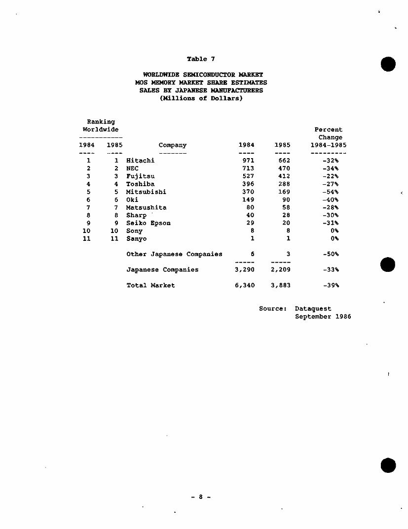
Table 7
WORLDWIDE SEMICONDUCTOR MARKET MOS MEMORY MARKET SHARE ESTIMATES SALES BY JAPANESE MANUFACTtJRERS
(Mi l l ions of Dollars)
Rank ing Worldwide
1984
1 2 3 4 5 6 7 8 9
10 11
1985
1 2 3 4 5 6 7 8 9
10 11
company
Hitachi NEC Fujitsu Toshiba Mitsubishi Oki Matsushita Sharp Seiko Epson Sony Sanyo
Other Japanese Companies
Japanese Companies
Total Market
1984
971 713 527 396 370 149 80 40 29 8 1
6
3,290
6,340
1985
662 470 412 288 169 90 58 28 20 8 1
3
2,209
3,883
Percent Change
1984-1985
-32% -34% -22% -27% -54% -40% -28% -30% -31%
0% 0%
-50%
-33%
-39%
Source: Dataquest September 1986
- 8
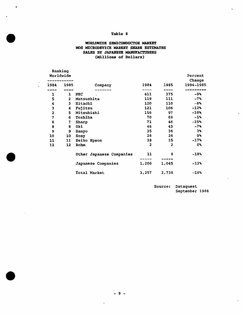
Table 8
WORLDWIDE SEMICONDUCTOR MARKET MOS MICRODEVICE MARKET SHARE ESTIMATES
SALES BY JAPANESE MANUFACTURERS (Millions of Dollars)
Rank; Lng Worldwide
1984
1 5 4 3 2 7 6 8 9
10 11 12
1985
1 2 3 4 5 6
7 8 9
10 11 12
Company
NEC Matsushita Hitachi Fujitsu Mitsubishi Toshiba Sharp Oki Sanyo Sony Seiko Epson Rohm
Other Japanese Companies
Japanese Companies
Total Market
1984
411 119 120 121 156 70 71 46 35 26 18 2
11
1,206
3,257
1985
375 111 110 106 97 69 46 43 36 26 15 2
9
1,045
2,739
Source:
Percent Change
1984-1985
-9% -7% -8%
-12% -38%
-1% -35% -7% 3% 0%
-17% 0%
-18%
-13%
-16%
Dataquest September 1986
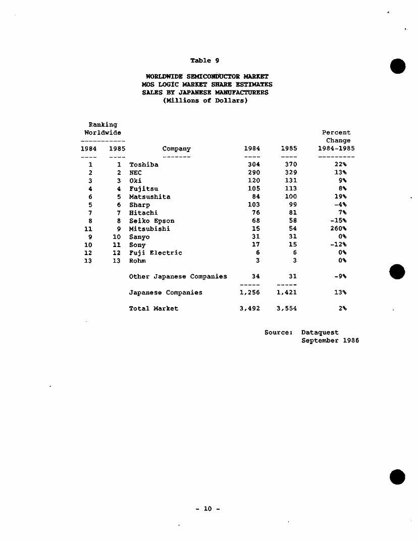
Table 9
WORLDWIDE SEMlCOMDtJCTOR MARKET MOS LOGIC MARKET SHARE ESTIMATES SALES BY JAPANESE MANUFACTURERS
(Millions of Dollars)
Hank: ing Worldwide
.984
1 2 3 4 6 5 7 8
11 9
10 12 13
1985
1 2 3 4 5 6 7 8 9
10 11 12 13
Compa
Toshiba NEC Oki Fujitsu Matsushita Sharp Hitachi Seiko Epson Mitsubishi Sanyo Sony Fuji Electric Rohm
Other Japanese Companies
Japanese Companies
Total Market
1984
304 290 120 105 84
103 76 68 15 31 17 6 3
34
1,256
3,492
1985
370 329 131 113 100 99 81 58 54 31 15 6 3
31
1,421
3,554
Percent Change
1984-1985
22% 13%
9% 8%
19% -4%
7% -15% 260%
0% -12%
0% 0%
-9%
13%
2%
Source: Dataguest September 1986
- 10 -

Table 10
WORLDWIDE SEMICONDUCTOR MARKET LINEAR MARKET SHARE ESTIMATES SALES BY JAPANESE MANUFACTURERS
(Millions of Dollars)
Rank ing Worldwide
1984
2 1 3 4 5 6 7 8 9
10 12 11 13
1985
1 2 3 4 5 6 7 8 9
10 11 12 13
Company
Matsushita NEC Toshiba Sanyo Hitachi Mitsubishi Rohm Sony Sanken Fujitsu Sharp Fuji Electric Oki
Other Japanese Companies
Japanese Companies
Total Market
1984
287 290 228 220 179 102 91 73 47 40 24 24 3
224
1,832
4,927
1985
305 300 235 228 189 111 85 76 46 42 28 24 3
235
1,907
4,767
Source:
Percent Change
1984-1985
6% 3% 2% 4% 6% 9%
-7% 4%
-2% 5%
n% 0% 0%
5%
4%
-3%
Dataguest September 1986
11
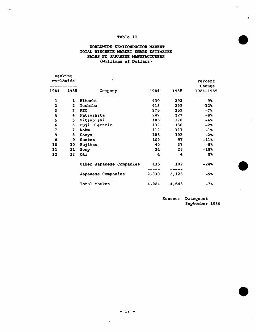
Table 11
WORLDWIDE SEMICONDUCTOR MARKET TOTAL DISCRETE MARKET SHARE ESTIMATES
SALES BY JAPANESE MANUFACTURERS (Millions of Do l lars)
Ranking Wor:
1984
1 2 3 4 5 6 7 9 8
10 11 12
Idwide
1985
1 2 3 4 5 6 7 8 9
10 11 12
Company
Hitachi Toshiba NEC Matsushita Mitsubishi Fuji Electric Rohm Sanyo Sanken Fujitsu Sony Oki
Other Japanese Companies
Japanese Companies
Total Market
1984
430 418 379 247 185 132 112 105 109 40 34 4
135
2,330
4,984
1985
392 368 351 227 178 130 111 103 97 37 28 4
102
2,128
4,648
Source:
Percent Change
1984-1985
-9% -12%
-7% -8% -4% -2% -1% -2%
-11% -8%
-18% 0%
-24%
-9%
-7%
Dataquest September 1986
12 -
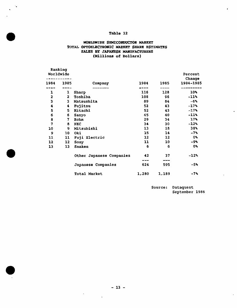
Table 12
WORLDWIDE SEMICONDUCTOR MARKET TOTAL OPTOELECTRONIC MARKET SHARE ESTIMATES
SALES BY JAPANESE MANUFACTURERS (Millions of Dollars)
Ranking Worldwide
1984 1985 Company
1 2 3 4 5 6 8 7 10 9
11 12 13
1 2 3 4 5 6 7 8 9
10 11 12 13
Sharp Toshiba Matsushita Fujitsu Hitachi Sanyo Rohm NEC Mitsubishi Oki Fuji Electric Sony Sanken
Other Japanese Companies
Japanese Companies
Total Market
1984
116 108 89 52 52 45 29 34 13 15 12 11 6
42
624
1,280
1985
128 96 84 43 43 40 34 30 18 14 12 10 6
37
595
1,189
Percent
Change 1984-1985
10% -ll-fe -6%
-n% -17% -11% 17%
-12% 38% -7% 0%
-9% 0%
-12%
-5%
-7%
Source: Dataquest September 1986
- 13
JAPANESE SEMICONDUCTOR MARKET
Japanese manufacturers dominated their home market, with 89.8 percent market share in 1985. (For Japanese market share splits by manufacturers' home base, see Market Share in Japan—Executive Summary, behind the Market Share tab of JSIS Volume I, Markets.) In the Japanese market, only one foreign-based manufacturer—Texas Instruments--is ranked among the top ten suppliers.
NEC, Toshiba, Hitachi, Matsushita, and Fujitsu were the top five suppliers to the Japanese market in 1985. These companies' sales accounted for 61.7 percent of the Japanese semiconductor market in 1985. Of these, Fujitsu suffered the most severe revenue decline, dropping 9 percent.
Two of the top ten suppliers—Sony and Sharp—actually increased their sales in Japan in 1985. All but $2 million of Sony's semiconductor sales were to the Japanese market, and the company surged ahead in almost all of its product families, including MOS memory, MOS logic, diodes, and optoelectronic devices. Sony has been a captive supplier for some time, and only entered the merchant market in 1983, so its small existing merchant sales base has provided plenty of room for growth. In addition, high levels of compact disk player production have given Sony an excellent captive market for laser diodes. Sharp was also able to capitalize on a Strong 1985 consumer market, in which it is a major player. The top ten suppliers to the market accounted for 82.3 percent of the total Japanese semiconductor market.
Top ranked foreign companies in the Japanese market in 1985 were Texas Instruments (number 8), Intel (number 14), Motorola (number 16), National Semiconductor (number 18), Philips-Signetics (number 19), AMD (niimber 20), Fairchild (number 21), and Analog Devices (number 22). However, foreign suppliers all told accounted for only 10.2 of the entire Japanese semiconductor market in 1985. Also, only one European company is listed in the top 25—Philips-Signetics. It must be noted here that the July 31 U.S.-Japan semiconductor trade agreement calls for increased penetration of the Japanese semiconductor market by foreign-based semiconductor firms, not solely by U.S. semiconductor firms; therefore, European firms have some hope for increased Japanese market access in the future.
Tables 13 through 24 rank the top worldwide manufacturers' semiconductor sales in Japan in 1984 and 1985.
NOTE
A complete set of market share tables by product for Japanese companies worldwide and for all companies into Japan was published in August 1986. This set of tables is entitled Market Share Estimates, and is filed behind the Market Share tab of JSIS Volume I, Markets. Please contact your JSIS binderholder for more information.
Patricia S. Cox
- 14
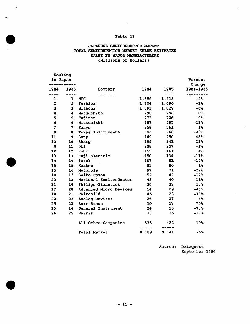
Table 13
JAPANESE SEMICONDUCTOR MARKET TOTAL SEMICONDUCTOR MARKET SHARE ESTIMATES
SALES BY MAJOR MANUFACTURERS (Millions of Dollars)
Ranking in Japan
984
1 2 3 4 5 6 7 8
11 10 9
12 13 14 16 15 18 20 21 17 19 22 29 23 24
1985
1 2 3 4 5 6 7 8 9
10 11 12 13 14 15 16 17 18 19 20 21 22 23 24 25
Company
NEC Toshiba Hitachi Matsushita Fujitsu Mitsubishi Sanyo Texas Instruments Sony Sharp Oki Rohm Fuji Electric Intel Sanken Motorola Seiko Epson National Semiconductor Philips-Signetics Advanced Micro Devices Fairchild Analog Devices Burr-Brown General Instriiment Harris
All Other Companies
Total Market
1984
1,556 1,104 1,093 798 772 757 358 342 169 198 209 155 150 107 85 97 52 45 30 54 45 26 10 24 18
535
8,789
1985
1,518 1,096 1,029
798 706 595 361 268 250 241 207 161 134 91 86 71 42 40 33 29 28 27 17 16 15
482
8,341
Percent Change
1984-1985
-2% -1% -6%
0% -9%
-21% 1%
-22% 48% 22% -1% 4%
-11% -15%
1% -27% -19% -11% 10%
-46% -38%
4% 70%
-33% -17%
-10%
-5%
Source: Dataguest September 1986
- 15 -
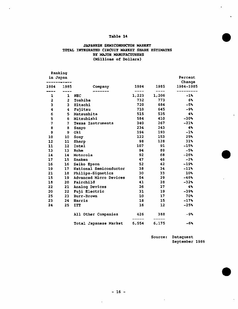
Table 14
JAPANESE SEMICONDUCTOR MARKET TOTAL INTEGRATED CIRCUIT MARKET SHARE ESTIMATES
BY MAJOR MANUFACTURERS (Millions of Dollars)
Ranking in
.984
1 2 3 4 6 5 7 8 9
10 12 11 13 14 17 16 19 21 15 18 22 20 25 23 24
Japan
1985
1 2 3 4 5 6 7 8 9
10 11 12 13 14 15 16 17 18 19 20 21 22 23 24 25
Company
NEC Toshiba Hitachi Fujitsu Matsushita Mitsubishi Texas Instruments Sanyo Oki Sony Sharp Intel Rohm Motorola Sanken Seiko Epson National Semiconductor Philips-Signetics Advanced Micro Devices Fairchild Analog Devices Fuji Electric Burr-Brown Harris ITT
All Other Companies
Total Japanese Market
1984
1,223 732 720 710 515 584 340 234 194 122 98
107 94 92 47 52 38 30 54 41 26 31 10 18 16
426
6,554
1985
1,206 773 684 645 535 410 267 243 193 153 128 91 89 68 46 42 34 33 29 28 27 19 17 15 12
388
6,175
Source:
Percent Change
1984-1985
-1% 6%
-5% -9%
4% -30% -21%
4% -1% 25% 31%
-15% -5%
-26% -2%
-19% -11% 10%
-46% -32%
4% -39% 70%
-17% -25%
-9%
-6%
Dataquest September 1986
- 16 -
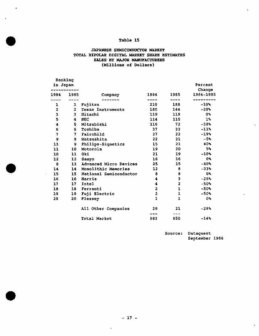
Table 15
JAPANESE SEMICONDUCTOR MARKET TOTAL BIPOLAR DIGITAL MARKET SHARE ESTIMATES
SALES BY MAJOR MANUFACTURERS (Millions of Dollars)
Rank: ing in Japan
1984
1 2 3 5 4 6 7 9
13 11 10 12 8
14 15 16 17 18 19 20
1985
1 2 3 4 5 6 7 8 9
10 11 12 13 14 15 16 17 18 19 20
Company
Fujitsu Texas Instruments Hitachi NEC Mitsubishi Toshiba Fairchild Matsushita Philips-Signetics Motorola Oki Sanyo Advanced Micro Devices Monolithic Memories National Semiconductor Harris Intel Ferranti Fuji Electric Plessey
All Other Companies
Total Market
1984
210 180 119 114 116 37 27 22 15 19 21 16 25 12 8 4 4 2 2 1
29
983
1985
188 144 119 115 72 33 22 21 21 20 19 16 15 8 8 3 2 1 1 1
21
850
Percent Change
1984-1985
-IC^ -20%
0% 1%
-38% -11% -19% -5% 40% 5%
-10% 0%
-40% -33%
0% -25% -50% -50% -50%
0%
-28%
-14%
Source: Dataquest September 1986
- 17
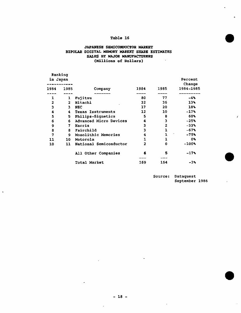
Table 16
JAPANESE SEMICONDUCTOR MARKET BIPOLAR DIGITAL MEMORY MARKET SHARE ESTIMATES
SALES BY MAJOR MT^NUFACTURERS
(M i l l ions of Do l lars)
Rank: ing in Japan
1984
1 2 3 4 5 6 9 8 7 11 10
1985
1 2 3 4 5 6 7 8 9
10 11
Company
Fujitsu Hitachi NEC Texas Instruments Philips-Signetics Advanced Micro Devices Harris Fairchild Monolithic Memories Motorola National S e m i c o n d u c t o r
All Other Companies
Total Market
1984
80 32 17 12 5 4 3 3 4 1 2
6
169
1985
77 36 20 10 8 3 2 1 1 1 0
6
164
Source:
Percent Change
1984-1985
-4% 13% 18%
-17% 60%
-25% -33% -67% -75%
0% -100%
-17%
-3%
Dataguest September 1986
- 18 -
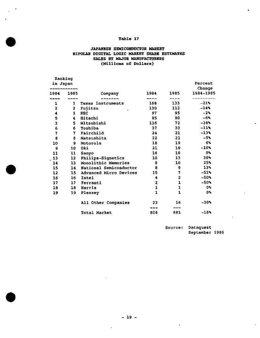
Table 17
JAPANESE SEMICONDUCTOR MARKET BIPOLAR DIGITAL LOGIC MARKET SHARE ESTIMATES
SALES BY MAJOR MANUFACTURERS (Millions of Dollars)
Rank: ing in Japan
1984
1 2 4 5 3 6 7 8 10 9 11
. 13 14 15 12 16 17 18 19
1985
1 2 3 4 5 6 7 8 9 10 11 12 13 14 15 16 17 18 19
Company
Texas Instruments Fujitsu NEC Hitachi Mitsubishi Toshiba Fairchild Matsushita Motorola Oki Sanyo Philips-Signetics Monolithic Memories National Semiconductor Advanced Micro Devices Intel Ferranti Harris Plessey
All Other Companies
Total Market
1984
168 130 97 85 116 37 24 22 18 21 16 10 8 8 15 4 2 1 1
23
806
1985
133 112 95 80 72 33 21 21 19 19 16 13 10 9 7 2 1 1 1
16
681
Source:
Percent Change
1984-1985
-21% -14% -2% -6% -38% -11% -13% -5% 6%
-10% 0%
30% 25% 13% -53% -50% -50% 0% 0%
-30%
-16%
Dataguest September 1986
- 19
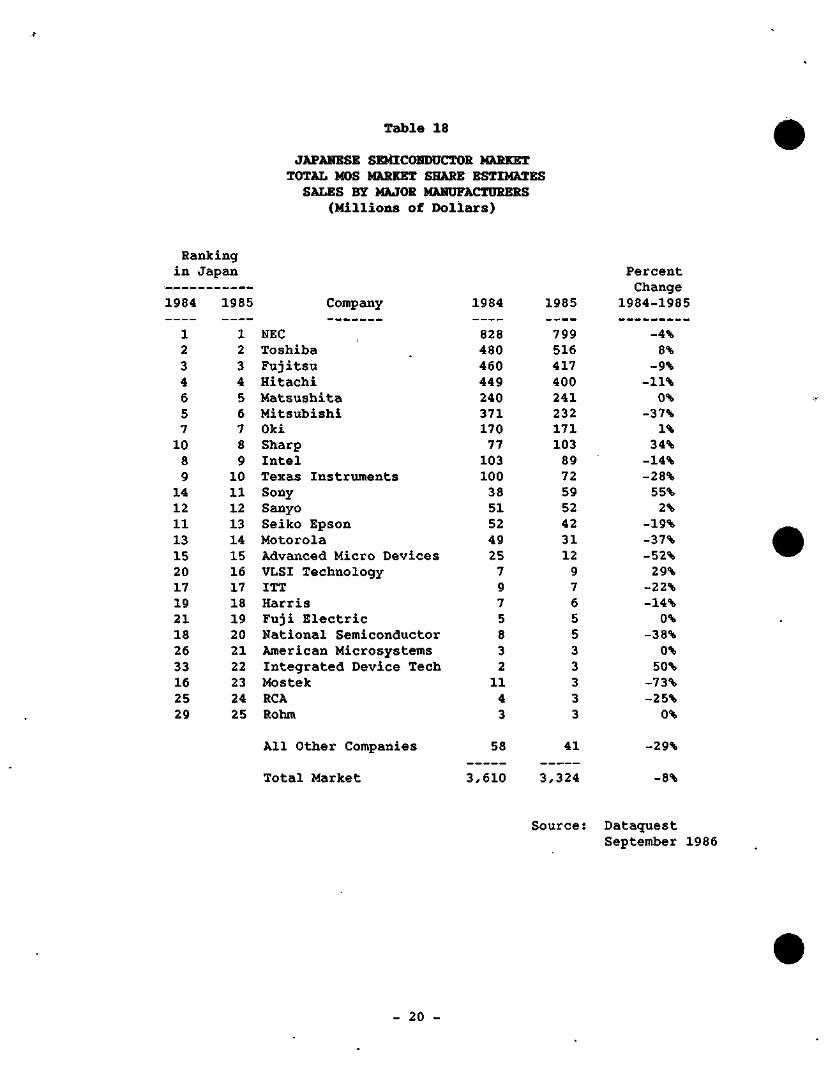
Table 18
JAPANESE SEMICONDUCTOR MARKET TOTAL MOS MARKET SHARE ESTIMATES SALES BY MAJOR MANUFACTURERS
(Millions of Dollars)
Rank: ing in Japan
1984
1 2 3 4 6 5 7 10 8 9
14 12 11 13 15 20 17 19 21 18 26 33 16 25 29
1985
1 2 3 4 5 6 7 8 9 10 11 12 13 14 15 16 17 18 19 20 21 22 23 24 25
Company
NEC Toshiba Fujitsu Hitachi Matsushita Mitsubishi Oki Sharp Intel Texas Instruments Sony Sanyo Seiko Epson M o t o r o l a Advanced Micro Devices VLSI Technology ITT Harris Fuji Electric National Semiconductor American M i c r o s y s t e m s Integrated Device Tech Mostek RCA Rohm
All Other Companies
T o t a l Market
1984
828 480 460 449 240 371 170 77 103 100 38 51 52 49 25 7 9 7 5 8 3 2
11 4 3
58
3,610
1985
799 516 417 400 241 232 171 103 89 72 59 52 42 31 12 9 7 6 5 5 3 3 3 3 3
41
3,324
Source:
Percent Change
1984-1985
-4% 8%
-9% -11%
0% -37%
1% 34%
-14% -28% 55% 2%
-19% -37% -52% 29%
-22% -14%
0% -38%
0% 50%
-73% -25%
0%
-29%
-8%
Dataquest September 1986
- 20

Table 19
JAPANESE SEMICONDUCTOR MARKET MOS MEMORY MARKET SHARE ESTIMATES
SALES BY MAJOR MANUFACTURERS (Millions of Dollars)
Rank: ing in Japan
1984
1 2 3 5 4 6 7 9 8
12 11 16 10 18 20 21 15 17 23
1985
1 2 3 4 5 6 7 8 9
10 11 12 13 14 15 16 17 18 19
Company
Hitachi NEC Fujitsu Toshiba Mitsubishi Matsushita Oki Intel Texas Instruments Sharp Seiko Epson Sony Advanced Micro Devices Xicor Harris Integrated Device Tech Micron Technology Seeg VLSI Technology
All Other Companies
Total Market
1984
354 315 271 148 235 68 46 29 32 10 10 4 11 3 2 2 5 3 2
30
1,580
1985
295 250 226 125 97 52 32 25 18 15 14 12 5 3 2 2 2 2 2
9
1,188
Source:
Percent Change
1984-1985
-17% -21% -17% -16% -59% -24% -30% -14% -44% 50% 40% 200% -55%
0% 0% 0%
-60% -33%
0%
-70%
-25%
Dataquest September 1986
- 21 -
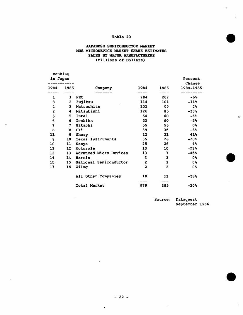
Table 20
JAPANESE SEMICONDUCTOR MARKET MOS MICRODEVICE MARKET SHARE ESTIMATES
SALES BY MAJOR MANUFACTURERS (Mi l l ions of Dollars)
Rank: ing in Japan
1984
1 3 4 2 5 6 7 8
11 9
10 13 12 14 15 17
1985
1 2 3 4 5 6 7 8 9
10 11 12 13 14 15 16
Company
NEC Fujitsu Matsushita Mitsubishi Intel Toshiba Hitachi Oki Sharp Texas Instruments Sanyo Motorola Advanced Micro Devices Harris National Semiconductor Zilog
All Other Companies
Total Market
1984
284 114 101 126 64 63 55 39 22 35 25 13 13 3 2 2
18
979
1985
267 101 99 85 60 60 55 36 31 28 26 10 7 3 2 2
13
885
Source:
Percent Change
1984-1985
-6% -11%
-2% -33% -6% -5%
0% -8% 41%
-20% 4%
-23% -46%
0% 0% 0%
-28%
-10%
Dataquest September 1986
22 -
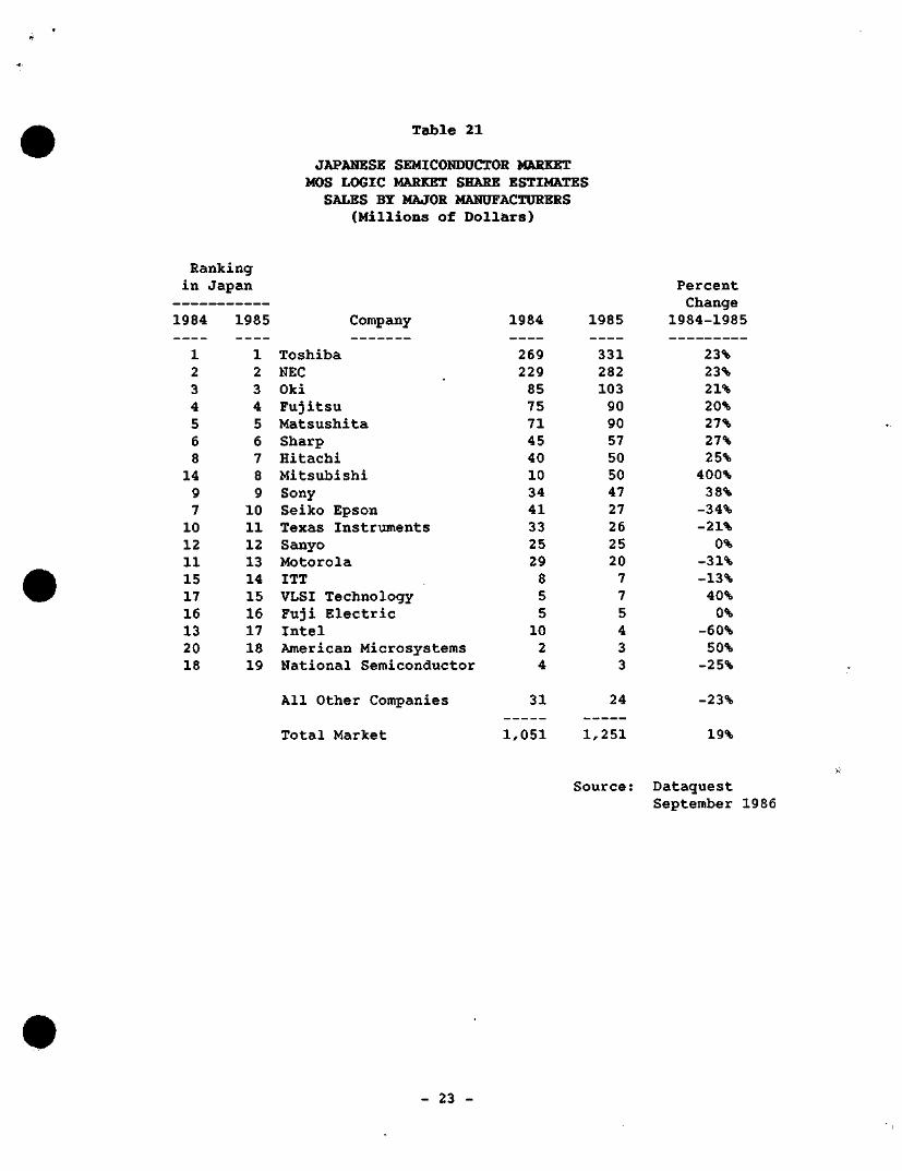
Table 21
JAPANESE SEMICONDUCTOR MAfiKET MOS LOGIC MARKET SHARE ESTIMATES SALES BY MAJOR MANUFACTURERS
(Mi l l ions of Dollars)
Rank: ing in Japan
1984
1 2 3 4 5 6 8
14 9 7 10 12 11 15 17 16 13 20 18
1985
1 2 3 4 5 6 7 8 9
10 11 12 13 14 15 16 17 18 19
Company
Toshiba NEC Oki Fujitsu Matsushita Sharp Hitachi Mitsubishi Sony Seiko Epson Texas Instruments Sanyo Motorola ITT VLSI Technology Fuji Electric Intel American Microsystems National Semiconductor
All Other Companies
Total Market
1984
269 229 85 75 71 45 40 10 34 41 33 25 29 8 5 5
10 2 4
31
1,051
1985
331 282 103 90 90 57 50 50 47 27 26 25 20 7 7 5 4 3 3
24
1,251
Source:
Percent Change
1984-1985
23% 23% 21% 20% 27% 27% 25%
400% 38%
-34% -21%
0% -31% -13% 40% 0%
-60% 50%
-25%
-23%
19%
Dataguest September 1986
23
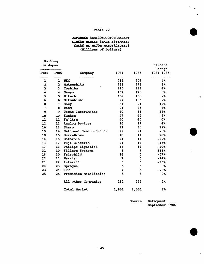
Table 22
JAPANESE SEMICONDUCTOR MARKET LINEAR MARKET SHARE ESTIMATES SALES BY MAJOR MANUFACTURERS
(Millions of Dollars)
Rank: ing in Japan
1984
1 2 3 4 5 6 8 7 9
10 11 12 16 15 19 14 13 17 31 18 22 21 24 23 25
1985
1 2 3 4 5 6 7 8 9 10 11 12 13 14 15 16 17 18 19 20 21 22 23 24 25
Company
NEC Matsushita Toshiba Sanyo Hitachi Mitsubishi Sony Rohm Texas Instruments Sanken Fujitsu Analog Devices Sharp National Semiconductor Burr-Brown Motorola Fuji Electric Philips-Signetics S i l i c o n Systems Fairchild Harris Intersil Sprague ITT Precision Monolithics
All Other Companies
Total Market
1984
281 253 215 167 152 97 84 91 60 47 40 26 21 22 10 24 24 15 3 14 7 8 6 7 5
282
1,961
1985
292 273 224 175 165 106 94 85 51 46 40 27 25 21 17 17 13 12 7 6 6 6 6 5 5
277
2,001
Source:
Percent Change
1984-1985
4% 8% 4% 5% 9% 9%
12% -7%
-15% -2%
0% 4%
19% -5% 70%
-29% -46% -20% 133% -57% -14% -25%
0% -29%
0%
-2%
2%
Dataquest September 1986
- 24 -
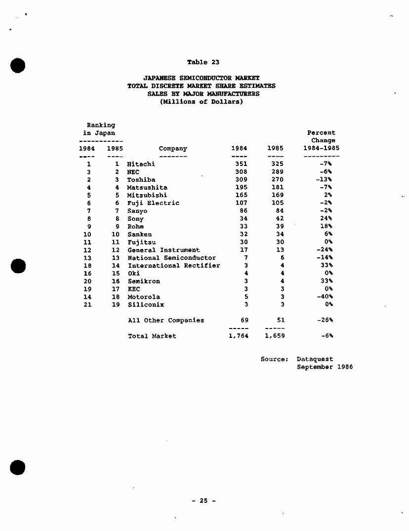
Table 23
JAPANESE SEMICONDUCTOR MARKET TOTAL DISCRETE MARKET SHARE ESTIMATES
SALES BY MAJOR MANUFACTURERS (Millions of Dollars)
Ranking in
984
1 3 2 4 5 6 7 8 9
10 11 12 13 18 16 20 19 14 21
Japan
1985
1 2 3 4 5 6 7 8 9
10 11 12 13 14 15 16 17 18 19
Company
Hitachi NEC Toshiba Matsushita Mitsubishi Fuji Electric Sanyo Sony Rohm Sanken Fujitsu General Instrument National Semiconductor International Rectifier Oki Semikron KEC Motorola Siliconix
All Other Companies
Total Market
1984
351 308 309 195 165 107 86 34 33 32 30 17 7 3 4 3 3 5 3
69
1,764
1985
325 289 270 181 169 105 84 42 39 34 30 13 6 4 4 4 3 3 3
51
1,659
Source:
Percent Change
1984-1985
-7% -6%
-13% -7%
2% -2% -2% 24% 18% 6% 0%
-24% -14% 33% 0%
33% 0%
-40% 0%
-26%
-6%
Dataguest September 1986
25 -
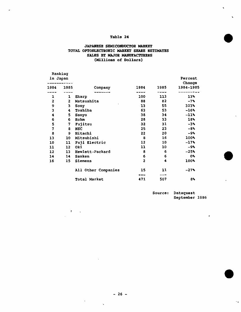
Table 24
JAPANESE SEMICONDUCTOR MARKET TOTAL OPTOELECTRONIC MARKET SHARE ESTIMATES
SALES BY MAJOR MANUFACTURERS (Millions of Dollars)
Ranking in Japan
1984
1 2 9 3 4 6 5 7 8 13 10 11 12 14 16
1985
1 2 3 4 5 6 7 8 9 10 11 12 13 14 15
Company
Sharp Matsushita Sony Toshiba Sanyo Rohm Fujitsu NEC Hitachi Mitsubishi Fuji Electric Oki Hewlett-Packard Sanken Siemens
All Other Companies
Total Market
1984
100 88 13 63 38 28 32 25 22 8 12 11 8 6 2
15
471
1985
113 82 55 53 34 33 31 23 20 16 10 10 6 6 4
11
507
Percent Change
1984-1985
13% -7%
323% -16% -11% 18% -3% -8% -9% 100% -17% -9% -25% 0%
100%
-27%
8%
Source: Dataquest September 1986
- 26
Dataqucst a company ot TIB; Run K Bi;i(iilrtLl Liirpoi a I ton
JAPANESE RESEARCH
NEWSLETTER
JSIS Code: Newsletters 1985-1986, JSIA 1986-35
IMPROVING INTERNATIONAL COMPETITIVENESS: A DATAQUEST VIEW
SUMMARY
Dataquest held a half-day seminar on July 31 to discuss international competitiveness in the semiconductor industry. Five Dataquest analysts and four outside speakers presented data and analysis on the topics of preserving strategic industries, the implications of trade cases for future competition, the status and future of the Japanese semiconductor industry, the future implications of shifting market shares in the semiconductor industry, intellectual property and trade restrictions, Korean manufacturers' competitiveness, and onshore versus offshore assembly.
The seminar coincided with an announcement from the White House that a final semiconductor trade agreement between the United States and Japan had been reached in the early hours of the morning. There was much speculation on the immediate and ultimate results of the agreement on inarket access and price monitoring. Most seminar attendees believed that price monitoring will be difficult to enforce. Skepticism was expressed on how much U.S. companies will actually be able to penetrate the Japanese semiconductor market, given the high percentage of consumer semiconductors used in Japan.
COMPETITIVENESS, MARKET SHARE. AND PRESERVATION OF THE INDUSTRY
Gene Norrett, associate director of Dataquest's Semiconductor Industry Group, noted the persistent decline of manufacturing as a percentage of the U.S. GNP, and the corresponding manufacturing trade imbalance. He pointed out the dominance of Japanese suppliers in the MOS memory business and noted that any company not involved in MOS memory—the largest single sector of the semiconductor industry--will lose market share as a result of the expected slower compound annual growth rate (CAGR) of the semiconductor industry excluding MOS memory.
1986 Dataquest Incorporated August—Reproduction Prohibited
The content of this report represents our InterpretatIon anid analysis of information generally available to the public or released by responsible individuals in the subject companies, but Is not guaranteed as to accuracy or completeness It does not contain material provided to us in confidence by our clients Individual companies reported on and analyzed by DATAQUEST, may be clients ol thIs and/or other DATAQUEST services This information Is not furnished in connection with a sale or offer to sell securities or in connection wIIh the solicitation of an offer to buy secunlIes This firm and its parent and/or their officers, stockholders, or members of their families may from time to time, have a long or short posItIon in the securities mentioned and may sell or buy such securities.
Taiyo Ginza Building / 7-14-16 Ginza. Chuo-ku / Tokyo 104, Japan / (03) 546-3191 / Telex J32768 1290 Ridder Park Drive / San Jose, CA 95131-2398/(408) 971-9000/Telex 171973
MOS memory manufacturers will gain market share. Japanese companies are also fast gaining ground in the semiconductor equipment business. The three top lead frame manufacturers, for example, are Japanese.
Patricia Cox, research analyst for the Japanese Semiconductor Industry Service, presented Dataguest's estimates of the phenomenal growth in Japanese semiconductor revenue (at a rate almost twice as fast as U.S. companies), the high growth in Japan's domestic semiconductor market, and the explosive growth in Japanese companies' semiconductor exports. These statistics, coupled with Japanese companies' extremely high R&D and capital spending, indicate continued trends toward Pacific Basin dominance of the semiconductor industry. Dataquest believes that Japanese-company worldwide semiconductor market share will exceed U.S.-company worldwide market share in 1986.
Although Japanese companies are gaining market share and the Japanese market has grown very fast, there are still a number of problems facing the Japanese semiconductor industry, according to Osamu Ohtake, associate director of the Japanese Semiconductor Industry Service. He pointed to the profit squeeze caused by the fast appreciation of the yen, the tremendous industry overcapacity, and the competitive threat of older industrial companies that are now branching out into semiconductors in an attempt to diversify. He concluded that win-win relationships should be formed between U.S. and Japanese companies in the form of synergistic alliances in manufacturing, sales, distribution, and development.
Dr. Mike Bae, president of Macro Group and consultant to Dataquest on the Korean semiconductor industry, discussed the current status of the Korean manufacturers. The hard times in Japan are creating the perfect opportunity for Korean companies to begin to penetrate the worldwide semiconductor market. He noted that Samsung has become the first Korean company to produce a working 1Mb DRAM. He cautioned that the Koreans must be careful to avoid dumping charges by pricing near the market level.
Anthony Perrotta, president of Amkor Electronics Inc., presented Amkor/Anam's view of onshore versus offshore assembly. Taking into account shifting geographic demand for semiconductors, the growing ASIC market, and shifting packaging types,, he examined the relative merits of onshore versus offshore assembly. He concluded that although some new assembly will be installed in the United States between now and 1990, the bulk of new assembly will be in the Far East.
TRADE. TRADE, AND TRADE
Two seminar speakers focused on the semiconductor trade agreement signed early July 31 between, the U.S. and Japanese governments.
Dr. William Finan, of Quick, Finan, and Associates, believes that the Japanese think that the ball game is over—and that they won. He pointed out, however, that the case that is potentially the most significant in its long-term effects has not yet been decided—that is, Texas Instruments' lawsuit against Japanese companies for patent infringement in
- 2
256K DRAMs. The case will most likely not be decided until next year, but it could potentially result in an embargo on the importation to the United States of all DRAMs made by the infringing companies, both in chip form and embedded in end equipment.
Dr. John Barton, professor of law at Stanford University, discussed the international status of intellectual property law but more particularly focused on the trade agreements. He believes that the market access issue is a qualitative problem that needs a qualitative solution. Regarding the price-monitoring system scheduled to begin this month, he does not believe that most companies will adhere to the minimum prices they are required to charge, because that would severely hamper their ability to sell their products. But Dr. Barton does believe that the legality of the agreement will be upheld in U.S. courts. The only possible counter argxament would be that true production costs are extremely difficult to calculate, thereby shedding doubt on the accuracy of the cost and pricing data used in enforcement of the agreement.
CONCLUSIONS
Sheridan Tatsuno, senior industry analyst for the Japanese Semiconductor Industry Service, concluded the seminar with a summary of the main points:
• Semiconductor industry dominance is shifting from the United States to Japan and Asia.
• Because Japan is currently facing economic problems associated with the high value of the yen and political pressure from the major economic powers, the country is pushing to achieve the next major technological breakthrough by focusing heavily on innovation and creativity.
• In light of the recent semiconductor agreement, U.S., European, and Asian vendors should seek alliances with Japanese OEMs to increase their market shares in Japan.
Bound seminar proceedings and a videotape of the seminar will soon be available. To purchase copies of either, please call JSIS at (408) 971-9000, extension 481.
Patricia S. Cox Sheridan Tatsuno
- 3 -
Dataquest aiLHtlpUMVul The l>un &• (trmlittcct Corponil ion
JAPANESE RESEARCH
NEWSLETTER
JSIS Code: Newsletters 1985-1986, JSIA 1986-34 Rev. 9/12/86
JAPANESE SEMICONDUCTOR APPLICATION TRENDS FIRST QUARTER 1986
SUMMARY
First quarter 1986 electronics/electric equipment production in Japan was ¥4.0 trillion ($19 billion), up 1.0 percent from the same period in 1985 but down 7.1 percent from the fourth quarter of 1985.
First quarter 1986 semiconductor consumption decreased by 4.7 percent compared with the first quarter of 1985, although it increased 1.0 percent over the ¥499.4 billion ($2.4 billion) reported in the fourth quarter of 1985.
We believe that equipment production value in 1986 will grow only slightly to ¥16.5 trillion ($100 billion at ¥165 per US$1), up from ¥16.4 billion ($68.9 billion) over 1985 due to the appreciation of the yen.
The high appreciation of the yen has also caused the first quarter GNP to drop by 0.5 percent in real terms from the previous quarter. The most significant impact of the yen appreciation has been a sharp drop in exports; they have decreased by 4.9 percent relative to fourth quarter 1985.
THE MARKET
Dataquest's Japanese Semiconductor Industry Service recently constructed a data base composed of 50 different types of major electronics/electrical equipment. We have analyzed these equipment types for their semiconductor usage, and have built up a semiconductor consumption data base as a check against the analysis of industry and government data.
© 1986 Dataquest Incorporated September—Reproduction Prohibited
The conlenl ol this report represents our interpretation and analysts of information generally available to ftie public or released by responsible individuals in ttie sub|ect companies, but is not guaranteed as to accuracy or completeness It does not contain material provided to us in confidence by our clients Individual companies reported on and analyzed by DATAQUEST, may be clients ol tfiis and/or ottter DATAQtJEST services Ttiis information is not furnished in connection with a sale or offer to sell securities or in connection with the solicitation ol an offer to buy securities This firm and its parent and/or their officers, stocl holders, or memtjers ol their families may from time to time, have a fong or short position in the securities mentioned and may sell or buy such securities
Taiyo Ginza Building / 7-14-16 Ginza, Chuo-ku / Tokyo 104, Japan / (03) 546-3191 / Telex J32768 1290 Ridder Park Drive / San Jose, CA 95131-2398 / (408) 971-9000 / Telex 171973
\
Table 1 shows the first quarter 1986 electronics production value as ¥1.8 trillion ($7.2 billion) for consumer electronics and ¥2.1 trillion ($8.2 billion) for industrial electronics. Compared with the same period last year, consumer electronics production decreased 2.7 percent, while industrial electronics production increased 4.3 percent. Industrial electronics production, however, declined 2.1 percent compared with the fourth quarter of 1985.
To facilitate the comparison with the U.S. and European markets, the same data converted to dollars are shown in Table 2. Total Japanese electronics production is expected to be $95.2 billion in 1986, achieving 36.9 percent growth. We have shown the market in dollars, but this really is of little use, since all of this growth is due to yen appreciation.
Table 3 shows the year-to-year quarterly comparisons of electronics equipment production in Japan based on the first quarter result. We forecast an overall 5.6 percent decrease for consiuner electronics and a 5.0 percent increase for industrial electronics in 1986. If this happens then we expect zero growth for total electronics production in 1986.
SEMICONDUCTOR CONSUMPTION
Table 4 shows Japanese semiconductor consumption in the first quarter by application category. In the first quarter of 1986, semiconductor consumption was ¥504.4 billion ($2.68 billion). Consumer semiconductor consumption was ¥141.3 billion ($0.75 billion) and industrial semiconductor consumption was ¥363.1 billion ($1.9 billion).
Figure 1 shows the composition of the semiconductor consumption for first quarter 1986. Because of the drive to produce industrial electronics, industrial semiconductor consumption increased t o 72 percent of the total in first quarter 1986 from 69.2 percent in first quarter 1985.
Consumer Electronics
Semiconductor consumption for consumer electronics in the first quarter of 1986 was ¥141.3 billion ($751.6 million). Among the consumer electronics products, digital audio disk players and video cameras grew rapidly. The estimated semiconductor consumption in the first quarter was ¥12.5 billion ($66.5 million) for video cameras, up 50.5 percent, and ¥10.3 billion ($54.8 million) for digital audio disk players, up 258.1 percent.
On the other hand, large decreases were observed in headphone stereos and tape recorders (including radiocassettes). Dataquest estimates that semiconductor consumption in headphone stereos and tape recorders was ¥2.4 billion ($12.8 million) and ¥8.7 billion ($46.3 million), respectively, and both decreased 36.1 percent compared with fourth quarter 1985.
2 -
y
Industrial Electronics
Generally speaking, semiconductor consumption in industrial electronics was not as bad as for consumer electronics. Comparing first quarter in 1986 versus fourth quarter 1985, we did not see large declines.
Although industrial semiconductor consumption declined 0.6 percent from the first quarter of 1985, it grew 2.3 percent compared with the fourth quarter.
In particular, we observed large increases in semiconductor consumption for input/output units, peripheral units, and telephone-related devices. Their growth ratios from the fourth quarter of 1985 were 86.2 percent, 71.4 percent, and 67.4 percent, respectively.
In the computer category, the semiconductor demands for personal computers and office computers were brisk, with consumption values of ¥33.4 billion ($177.7 million), up 28 percent, and ¥9 billion ($47.8 million, up 31 percent, respectively.
Nagayoshi Nakano
- 3 -
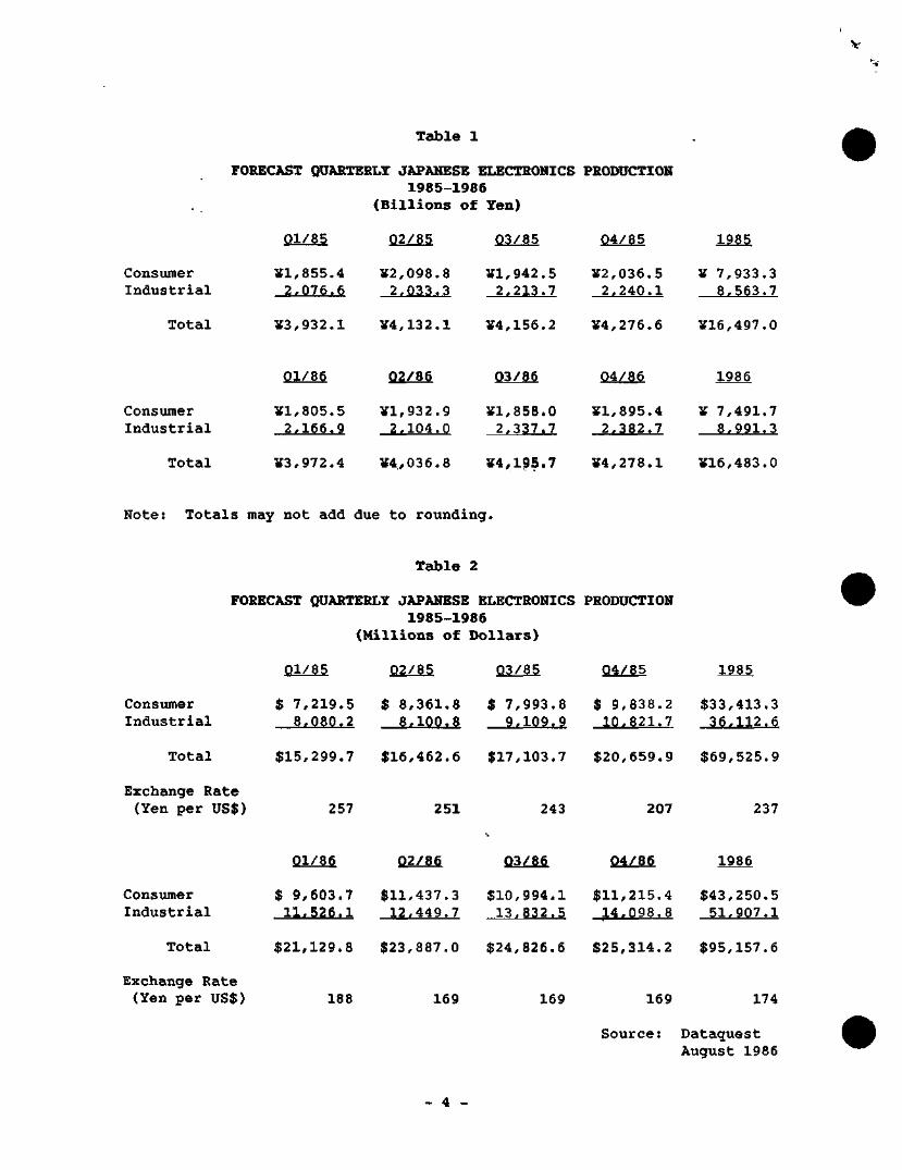
Table 1
FORECAST QUARTERLY JAPANESE ELECTRONICS PRODUCTION 1985-1986
(Billions of Yen)
V
01/85 02/85 03/85 04/85 1985
Consumer Industrial
»1,855.4 2,076.6
¥2,098.8 2,033.3
¥1,942.5 2,213.7
¥2,036.5 2,240.1
¥ 7,933.3 8,563.7
Total ¥3,932.1 ¥4,132.1 ¥4,156.2 ¥4,276.6 ¥16,497.0
01/86 02/86 03/86 04/86 1986
Consumer Industrial
¥1,805.5 2,166.9
¥1,93 2.9 2,104.0
¥1,858.0 2.337.7
¥1,895.4 2.382.7
¥ 7,491.7 8,991.3
Total ¥3,972.4 ¥4,036.8 ¥4,195.7 ¥4,278.1 ¥16,483.0
Note: Totals may not add due t o rounding.
Table 2
FORECAST QUARTERLY JAPANESE ELECTRONICS PRODUCTION 1985-1986
(Millions of Dollars)
Consumer Industrial
01/85
$ 7,219.5 8,080.2
02/85
$ 8,361.8 8.100.8
03/85
$ 7,993.8 9.109.9
04/85
$ 9,836.2 10.821.7
1985
$33 , 36 .
, 413 , ,112 ,
.3
.6
Total $15,299.7 $16,462.6 $17,103.7 $20,659.9 $69,525.9
Exchange Rate (Yen per US$) 257 251 243 207 237
01/8^ 02/86 03/86 04/86 1986
Consumer Industrial
$ 9,603.7 11.526.1
$11,437.3 12.449.7
$10,994,1 13.832.5
$11,215.4 14,098.8
$43,250.5 51.907.1
Total $21,129.8 $23,887.0 $24,826.6 $25,314.2 $95,157.6
Exchange Rate (Yen per US$) 188 169 169 169 174
Source: Dataquest August 1986
- 4 -
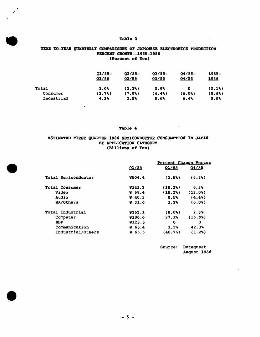
Table 3
YEAR-TO-YEAR QUARTERLY GOMPARISONS OF JAPANESE ELECTRONICS PRODUCTION PERCENT GROWTH—1985-1986
(Percent of Yen)
Ql/85-Ql/86
Q2/85-02/86
Q3/85-03/86
Q4/85-04/86
1985-1986
Total Consumer Industrial
1.0% (2.7%) 4.3%
(2.3%) (7.9%) 3.5%
0.9% (4.4%) 5.6%
0 (6.9%) 6.4%
(0.1%) (5.6%) 5.0%
Table 4
ESTIMATED FIRST QUARTER 1986 SEMICONDUCTOR CONSUMPTION IN JAPAN BY APPLICATION CATEGORY
(Billions of Yen)
Total Semiconductor
01/86
¥504.4
Percent Change Versus 01/85 04/85
(3.5%) (6.8%)
Total Consumer Video Audio HA/Others
Total Industrial Computer HDP Communication Industrial/Others
¥141.3 ¥ 69.4 ¥ 40.3 ¥ 31.6
¥363.1 ¥106.6 ¥125.5 ¥ 65.4 ¥ 65.6
(10.2%) (10.2%) 0.5% 3.3%
(0.6%) 27.1%
0 1.3%
(40.7%)
6.3% (12.0%) (4.4%) (6.0%)
2.3% (16.8%)
0 42.0% (1.2%)
Source; Dataquest August 1986
- 5 -
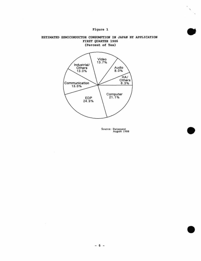
Figure 1
ESTIMATED SEMICONDUCTOR CONSTIMPTION IN JAPAN BY APPLICATION FIRST QUARTER 1986 (Percent of Yen)
Source: Dataquest August 1986
- 6 -
DataQuest a conipaiiv ol The L)u n tSJ Bt-jdslicpt Corpbnitiun
JAPANESE RESEARCH
NEWSLETTER JSIS Code: Newsletters 1985-1986, JSIA
1986-33
JAPANESE SEMICONDUCTOR MARKET QUARTERLY UPDATE: HIGH YEN WREAKING HAVOC ON JAPANESE CONSUMPTION
SUMMARY
Dataquest has tempered its forecast for the 1986 Japanese semiconductor market as the devastating effects of the high yen make themselves felt. We have lowered our forecast for yen growth in Japanese consumption to a meager 1.2 percent in 1986, followed by a healthy 22.2 percent in 1987. At the same time, due to a still-rising yen, we expect dollar consumption in Japan to grow a hefty 39.1 percent in 1986, followed by slower growth of 25.3 percent in 1987. However, because we have assumed a flat exchange rate of ifl69 per US$1 from the second quarter of 1986 through the fourth quarter of 1987, real growth (i.e., yen growth) is expected to be considerably higher in 1987 than in 1986.
Figure 1 shows quarter-to-quarter percent growth in yen for the Japanese semiconductor market from the first quarter of 1985 through the fourth quarter of 1987. Figure 2 presents the same data in dollars.
EFFECTS OF CURRENCY FLUCTUATIONS
The effects of the extreme drop in the dollar and concomitant rise in the yen must not be underestimated. The high yen is making Japanese-manufactured electronic equipment—both consumer and industrial electronics—uncompetitive in dollar terms. To counter this effect and maintain profitability, Japanese firms are beginning to manufacture this end equipment in Korea, Taiwan, and other Asian countries where they can save on cheap labor rates. As a result, many semiconductors (and other components) that normally would be consumed in equipment made in Japan are now being consumed in equipment made and marketed by Japanese companies in other Asian countries. This shift in consumption has the effect of dramatically increasing the Asian semiconductor market in 1986.
Our forecast uses actual quarterly exchange rates through the second quarter of 1986; from the third quarter of 1986 through the fourth quarter of 1987 we have used the Q2/86 exchange rate of Sfl69 per US$1.
© 1986 Dataquest Incorporated August—Reproduction Prohibited
The content of thIs report represents our interpretation and analysis of Information generally available to the public or released by responsible individuals in the subject companies, but is not guaranteed as to accuracy or completeness It does not contain material provided to us in confidence by our clients. Individual companies reported on and analyzed by DATAQUEST, may be clients of this and/or othier DATAQUEST services This information is not furnished in connection with a sale or offer to sell securities or in connection with the solicitation ot an offer to buy securities This firm and its parent and/or Iheir officers, stockholders, or members ot their families may, from time to time, have a iong or short position in the securities mentioned and may sell or buy such securities
Taiyo Ginza Building / 7-14-16 Ginza, Chuo-ku / Tokyo 104, Japan / (03) 546-3191 / Telex J32768 1290 Ridder Park Drive / San Jose, CA 95131-2398 / (408) 971-9000 / Telex 171973
Most Japanese semiconductor companies are assuming a 1986 average exchange rate of approximately if 170 per US$1; however, the dollar continues to hit new lows against the yen, reaching a new record of 5fl55.5 on July 21.
ASSUMPTIONS
The following observations and assumptions underlie our current forecast for the Japanese semiconductor market:
• A consumption shift is taking place in which Japanese market consumption is moving to Asia.
• This shift is most prevalent in linear ICs and discrete semiconductors for the consumer electronics market, both of which are expected to show negative growth in 1986.
• We expect optoelectronic growth to be stronger than any other category of semiconductor in 1986, due to the strong consumption of semiconductor lasers and ultrabright LEDs in consumer and automotive products.
• Consumption is forecast to rebound in 1987 (although not as much as our previous forecast indicated) aided by a stable yen, increased purchasing of U.S.-made semiconductors, and a generally healthier worldwide marketplace for electronic equipment.
Our quarterly forecast, in both yen and dollars, is shown in Tables 1 mnh d . through 4.
DATAQUEST CONCLDSIONS
Oataquest believes t:hat, because of rapid yen appreciation, the Japanese semiconductor market will grow to be the world's largest in 1986, at aJjnost $12 billion. Although this figure inflates actual growth due to the dramatic ascent of the yen, it does have significant effects. Among these are:
• Because of this high growth, we expect Japanese semiconductor manufacturers to score large gains in worldwide market share in 1986. Our current estimates are that t:he Japanese companies will grow at least 30 percent (in dollars) in 1986 semiconductor revenue.
• We anticipate competition in the always highly competitive Japanese market to become even fiercer than usual, causing pricing pressure on all semiconductor products.
Patricia S. Cox Osamu Ohtake
- 2 -
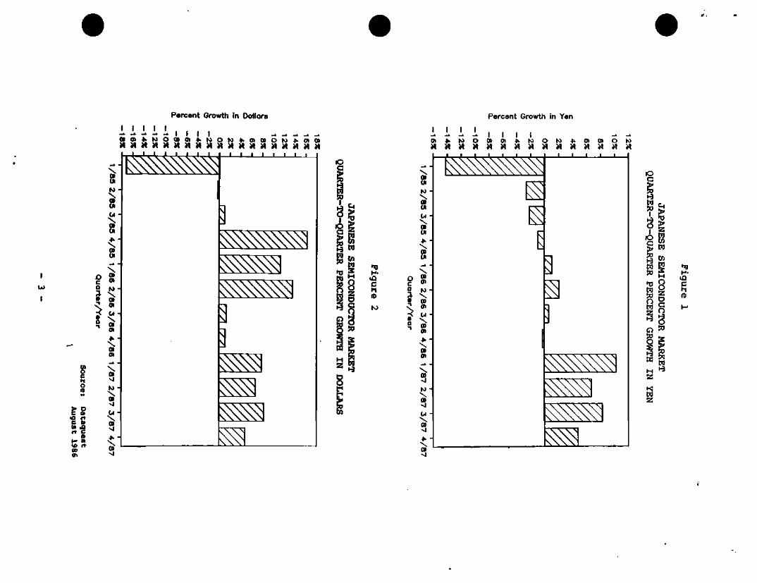
Percent Growth In Dollars Percent Growth In Yen
I
u>
I
I I I I a 0) i ' M M M M M
'^ 01 M A
\ o u IS) -\
u \ 0>
<-•
\ o 2 c » i \ • d - »
u \ a 01
> a o 1
o
> o C Bl to rt C 01
iJ-g t ' m <C f t 00 0\
ot 01
\ n vj N -| \ on vj 01
\ m v| *> \ OD vj
K
00 M
J I I L
O M ^ 0) 09 M M M M M
^ ^ ^ ^ ^ ^ ^ ^ ^
^ ^ ^ ^
^ ^
^
^
^
^
lA C M (D
to
P
i i i i I . I I 0 ) • ^ ^ > o o D O ) . ( > • l > J O ^ > . ^ o > O D O l o M M M M M M M M M M M M M i t M
03 C K n>
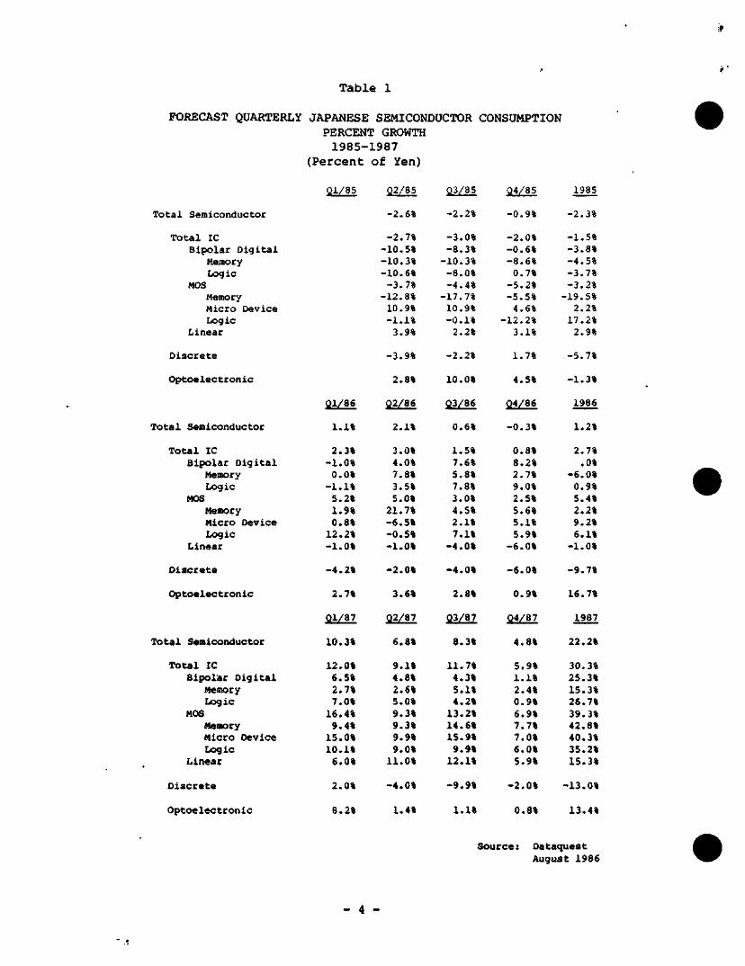
Table 1
FORECAST QUARTERLY JAPANESE SEMICONDUCTOR CONSUMPTION PERCENT GROWTH 1985-1987
(Percent of Yen)
Ql/85
Total Semiconductor
Total IC Bipolar Digital
Memory Logic
MOS Memory Micro Device Logic
Linear
Discrete
Optoelectronic
Total Semiconductor
Total IC Bipolar Digital
Memory Logic
HOS Memory Micro Device liogic
Linear
Discrete
Optoelectronic
Total Semiconductor
Total IC Bipolar Digital
Memory Logic
MOS Memory Micro Device Logic
Linear
Discrete
Optoelectronic
Q2/85
-2.6%
-2.7% •10.5% •10.3% •10.6% -3.7% •12.8% 10.9% -i.1% 3.9%
Q3/85
-2.2%
-3.0% -8.3% -10.3% -8.0% -4.4% -17.7% 10.9% -0.1% 2.2%
Q4/85
-0.9%
-2.0% -0.6% -8.6% 0.7%
-5.2% -5.5% 4.6%
-12.2% 3.1%
1985
-2.3%
-1.5% -3.8% -4.5% -3.7% -3.2% -19.5%
2.2% 17.2% 2.9%
-3.9% -2.2% 1.7% -5.7%
Ql/86
1.1%
2.3% -1.0% 0.0%
-1.1% 5.2% 1.9% 0.8% 12.2% -1.0%
-4.2%
2.7%
Ql/87
10.3%
12.0% 6.5% 2.7% 7.0% 16.4% 9.4% 15.0% 10.1% 6.0%
2.0%
8.2%
2.8%
Q2/86
2.1%
3.0% 4.0% 7.8% 3.5% 5.0%
21.7% -6.5% -0.5% -1.0%
-2.0%
3.6%
Q2/87
6.8%
9.1% 4.8% 2.6% 5.0% 9.3% 9.3% 9.9% 9.0% 11.0%
-4.0%
1.4%
10.0%
Q3/86
0.6%
1.5% 7.6% 5.8% 7.8% 3.0% 4.5% 2.1% 7.1%
-4.0%
-4.0%
2.8%
03/87
8.3%
11.7% 4.3% 5.1% 4.2% 13.2% 14.6% IS.9% 9.9% 12.1%
-9.9%
1.1%
4.5%
Q4/86
-0.3%
0.8% 8.2% 2.7% 9.0% 2.5% 5.6% 5.1% 5.9%
-6.0%
-6.0%
0.9%
24/87
4.8%
5.9% 1.1% 2.4% 0.9% 6.9% 7.7% 7.0% 6.0% 5.9%
-2.0%
0.8%
-1.3%
1986
1.2%
2.7% .0%
-6.0% 0.9% 5.4% 2.2% 9.2% 6.1%
-1.0%
-9.7%
16.7%
1987
22.2%
30.3% 25.3% 15.3% 26.7% 39.3% 42.8% 40.3% 35.2% 15.3%
-13.0%
13.4%
Source: Dataquest Augus t 1986
- 4 -
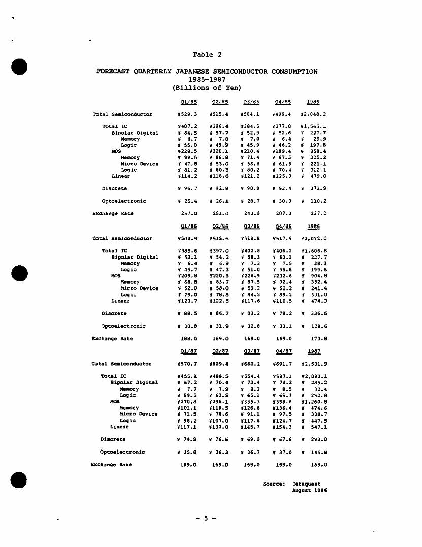
Table 2
FORECAST QUARTERLY JAPANESE SEMICONDUCTOR CONSUMPTION 1985-1987
(Billions Of Yen)
Total Semiconductor
Total IC Bipolar Digital
Memory Logic
MOS Memory Micro Device Logic
Linear
Discrete
Optoelectronic
Exchange Rate
Total Semiconductor
Total IC Bipolar Digital
Memory
Logic MOS
Memory
Micro Device Logic
Linear
Discrete
Optoelectronic
Exchange Rate
Total Semiconductor
Total IC
Bipolar Digital Memory
Logic
MOS Memory Micro Device
Logic Linear
Discrete
Optoelec tronic
Exchange Rate
(21/85
^529.3
*407.2
¥ 64.S i 8.7 i 55.8 iF228.S
» 99.5 t 47.8 )f 81.2 If 114.2
< 96.7
1 25.4
257.0
Ql/86
yS04.9
!f385.6 i 52.1 1 6.4 If 45.7 ¥209.8
If 68.8
f 62.0
* 79.0 !fl23.7
If 88.5
f 30.8
188.0
01/87
JS70.7
»455.1
i 67.2 i 7.7
» 59.5
¥270.8
¥101.1 ¥ 71.5
¥ 98.2
¥117.1
¥ 79.8
¥ 35.8
169.0
22/85
¥515.4
¥396.4 ¥ 57.7
¥ 7.8 ¥ 49.^
¥220.1
¥ 86.8 ¥ 53.0 ¥ 80.3
¥118.6
¥ 92.9
¥ 26.1
251.0
22/86
¥515.6
¥397.0 ¥ 54.2 ¥ 6.9
¥ 47.3 ¥220.3
¥ 83.7 ¥ 58.0
¥ 78.6
¥122.5
¥ 86.7
¥ 31.9
169.0
Q2/87
¥609.4
¥496.5 ¥ 70.4
¥ 7.9
¥ 62.5
¥296.1
¥110.5
¥ 78.6
¥107.0 ¥130.0
¥ 76.6
¥ 36.3
169.0
Q3/85
¥504.1
¥384.5
¥ 52.9 ¥ 7.0 ¥ 45.9 ¥210.4
¥ 71.4 ¥ 58.8 ¥ 80.2
¥121.2
¥ 90.9
¥ 28.7
243.0
03/8 6
¥518.8
¥402.8 ¥ 58.3 ¥ 7.3
¥ 51.0 ¥226.9
¥ 87.5 ¥ 59.2
¥ 84.2
¥117.6
¥ 83.2
¥ 32.8
169.0
23/87
¥660.1
¥554.4 ¥ 73.4
¥ 8.3
¥ 65.1
¥335.3
¥126.6 ¥ 91.1
¥117.6 ¥145.7
¥ 69.0
¥ 36.7
169.0
Q4/85
¥499.4
¥377.0 ¥ 52.6
¥ 6.4 ¥ 46.2 ¥199.4
¥ 67.5 ¥ 61.5 ¥ 70.4
¥125.0
¥ 92.4
¥ 30.0
207.0
24/86
¥517.5
¥406.2
¥ 63.1 ¥ 7.5 ¥ 55.6
¥232.6 ¥ 92.4
¥ 62.2 ¥ 89.2
¥110.5
¥ 78.2
¥ 33.1
169.0
24/87
¥691.7
¥587.1
¥ 74.2
¥ 8.5 ¥ 65.7
¥358.6
¥136.4 ¥ 97.5
¥124.7
¥154.3
¥ 67.6
¥ 37.0
169.0
¥2
¥1 ¥ ¥ ¥ ¥ ¥ ¥ ¥ ¥
¥
¥
¥2
¥1 ¥ ¥ ¥ ¥ ¥ ¥ ¥ ¥
¥
¥
¥2
¥2 ¥ ¥ ¥ ¥1 ¥ ¥ ¥ ¥
¥
¥
L985
,048.2
,565.1 227.7
29.9 197.8
858.4
325.2 221.1 312.1
479.0
372.9
110.2
237.0
1986
,072.0
,606.8 227.7
28.1 199.6 904.8
332.4
241.4
331.0
474.3
336.6
128.6
173.8
1987
,531.9
,093.1 285.2
32.4
252.8
,260.8
474.6 338.7
447.5 547.1
293.0
145.8
169.0
Source: Dataquest August 1986
- 5 -
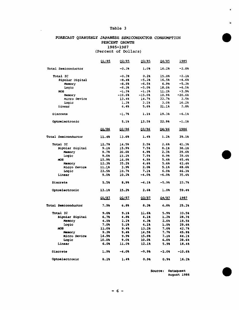
T a b l e 3
FORECAST QUARTERLY JAPANESE SEMICONDUCTOR CONSUMPTION PERCENT GROWTH
1985-1987 ( P e r c e n t of D o l l a r s )
T o t a l Semiconductor
T o t a l IC Bipolar Digital
Memory Logic
MOS Memory Micro Device Logic
Linear
Discrete
Optoelectronic
Total Semiconductor
Total IC Bipolar Digital
Memory Logic
MOS Memory Micro Device Logic
Linear
Discrete
Optoelectronic
Total Semiconductor
Total IC Bipolar Digital
Memory Logic
MOS Memory Micro Device Logic
Linear
Discrete
Optoelectronic
Q V 8 5 .
Q l / 8 6
11 .4%
12.7% 9 . 1% 9.7% 9.0%
15.9% 12.3% 1 1 . 1 % 23.5%
9.0%
5.5%
13.1%
2V87
7.9%
9.0% 6.7% 4 .5% 7.0%
11 .0% 9.3%
14.9% 10.0%
6.0%
1.9%
8.2%
Q2/85
- 0 . 3 %
- 0 . 3 % -8 .4% - 8 . 8 % - 8 . 3 % - 1 . 3 %
- 1 0 . 6 % 13.4%
1.3% 6.4%
- 1 . 7 %
5 .1%
Q2 /86
13.6%
14.5% 15.9% 20 .6% 15.2% 16.8% 35 .2%
3.9% 10.7% 10 .2%
8.9%
15.2%
2 2 / 8 7
6.8%
9 . 1 % 4.8% 2.2% 5 . 1% 9.4% 9.4% 9.9% 9.0%
11 .0%
- 4 . 0 %
1.4%
2 3 / 8 5
1.0%
0.2% - 5 . 2 % - 6 . 5 % - 5 . 0 % - 1 . 3 %
- 1 5 . 0 % 14.7%
3 .1% 5.6%
1.1%
13.5%
2 3 / 8 6
1.4%
2.5% 7.5% 4.9% 7.9% 4.8% 4.6% 2.0% 7 .1%
- 4 . 0 %
- 4 . 1 %
2.6%
2 3 / 8 7
8.3%
11.6% 4 . 1% 4.3% 4 . 1 %
13.2% 14.5% 15.9% 10.0% 1 2 . 1 %
- 9 . 9 %
0.9%
Q4/85
16.2%
15 .0% 16 .5%
6.9% 18.0% 11.2% 10.9% 22.7%
3.0% 2 1 . 1 %
1 9 . 3 %
22 .9%
Q4 /86
1.2%
2.6% 8 .1% 2.3% 8.9% 5.6% 5.6% 5 .1% 6.0%
- 6 . 0 %
- 5 . 9 %
1.0%
2 4 / 8 7
4.8%
5.9% 1.2% 2.0% 1.0% 7.0% 7.7% 7 . 1 % 6.0% 5.9%
- 2 . 0 %
0.9%
1985
- 2 . 8 %
- 2 . 1 % -4 .6% - 5 . 3 % - 4 . 5 % - 3 . 9 %
- 2 0 . 6 % 2.5%
16.2% 2.8%
- 6 . 1 %
- 1 . 1 %
1986
3 9 . 1 %
41.3% 38 .1% 29.6% 39.4% 45 .4% 42.4% 48.6% 46 .3% 35 .4%
23 .7%
59.4%
1987
25 .3%
33.5% 28 .3% 18.5% 29.6% 42 .7% 45 .8% 4 4 . 1 % 38 .6% 18.4%
- 1 0 . 6 %
16.2%
Source: Oataquest Augus t 1986
- 6 -
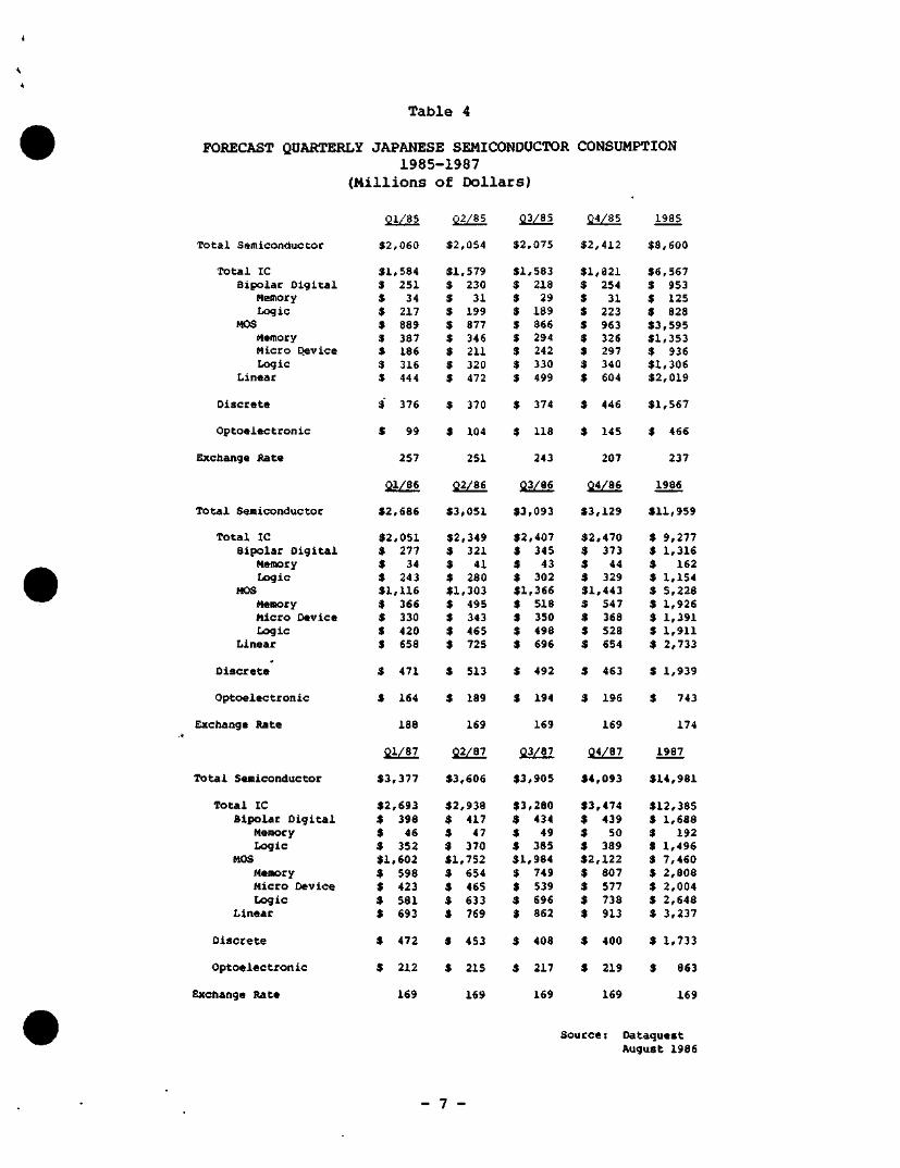
Table 4
FORECAST QUARTERLY JAPANESE SEMICONDUCTOR CONSUMPTION 1985-1987
(Millions Of Dollars)
Total Semiconductor
Total IC Bipolar Digital
Memory Logic
MOS Memory Micro Device Logic
Linear
Discrete
Optoelectronic
Exchange Rate
Total Semiconductor
Total IC Bipolar Digital
Memory Logic
MOS Memory Micro Device Logic
Linear
Discrete
Optoelectronic
Exchange Rate
Total Semiconductor
Total IC Bipolar Digital
Memory Logic
MOS Memory Micro IDevice Logic
Linear
Discrete
Optoelectronic
Exchange Rate
gV85
$2
31 3 $ $ $ 3 $ 3 3
3
$
,060
,584 251 34 217 889 387 186 316 444
376
99
257
Ql/86
$2
$2 3 $ $ $1 $ $ 3 3
3
3
,686
,051 277 34
243 ,116 366 330 420 658
471
164
188
21/87
33,
32 3 3 3 31, 3 3 3 3
3
3
,377
,693 398 46 352 ,602 598 423 581 693
472
212
169
22/85
$2
31 3 3 3 3 3 3 3 3
3
3
,054
,579 230 31 199 877 346 211 320 472
370
104
251
Q2/86
33
32 3 3 3 31 3 3 3 3
3
3
,051
,349 321 41
280 ,303 495 343 465 725
513
189
169
22/87
$3
32 3 3 3 31 3 3 3 3
3
3
,606
,938 417 47 370 ,752 654 465 633 769
453
215
169
23/85
32
31 $ 3 3 3 3 3 3 3
3
3
,075
,583 218 29
189 866 294 242 330 499
374
118
243
Q3/86
33
32 3 3 3 31 3 3 3 3
3
3
,093
,407 345 43 302 ,366 518 350 498 696
492
194
169
23/87
33
53 3 3 5 31, 3 3 3 3
3
3
,905
,280 434 49
385 ,984 749 539 696 862
408
217
169
Q4/85
32,
31, 3 3 3 3 3 3 3 3
3
3
r412
,821 254 31
223 963 326 297 340 604
446
145
207
Q4/86
33
32 3 3 3 31 3 3 3 3
3
3
,129
,470 373 44 329 ,443 547 368 528 654
463
196
169
24/87
34
33 3 3 3 32 3 3 3 3
3
3
,093
,474 439 50
389 ,122 807 577 738 913
400
219
169
1985
$8
36 3 3 3 33 31 3 31 32
31
3
,600
,567 953 125 828 ,595 ,353 936 ,306 ,019
,567
466
237
1986
311,959
3 3 3 3 3 3 3 3 3
3
3
9,277 1,316 162
1,154 5,228 1,926 1,391 1,911 2,733
1,939
743
174
1987
314,981
312,385 3 3 3 3 $ 3 3 3
3
3
1,688 192
1,496 7,460 2,808 2,004 2,648 3,237
1,733
863
169
Source: Dataquest August 1986
- 7 -
DataQuest a tumpativ 1)1 rHtnuiiR"Rr:»k lrtrtCiif!iiira liiM
JAPANESE RESEARCH
NEWSLETTER
JSIS Code: Newsletters 1985-1986, JSIA 1986-32
DOING BIGH-TECHNOLOGY BUSINESS IN KOREA
SUMMARY
This newsletter is the second to supplement the Korean Semiconductor Industry Analysis (KSIA) that was published in March 1986. (For more information on the 150-page, in-depth analysis, please contact Maureen Davies at (408) 971-9000, extension 481.)
As described briefly in Chapter 7 of KSIA, the Korean government selected nine strategic industries and placed special emphasis on developing approximately 600 technologies essential to them. The semiconductor industry is one of these; the other industries are computer materials, biochemicals, bioengineering, precision machinery, plant engineering, textiles, and energy resources. For these strategic industries, the government offers financial and technological support to individuals, companies, and venture groups seeking to establish new technology-intensive businesses using up-to-date technology.
Dataquest has prepared the following summary of "what-to-do" and "how-to-do-it" if one desires to enter or participate in the fast-growing high-technology industries in Korea,
INITIAL PHASE
It is very important to assess the basic business strategy of your company before entering the market in Korea. The following steps will guide you in planning the initial phase.
Type of Business
Trading; Import/Export
Without Your Own Product; Pure Trading - Check the list of products banned from Korea. (This list is available from the Korean Ministry of Electronics.) In general, if a high-technology product is
© 1986 Dataquest Incorporated July—Reproduction Prohibited
Ttie content of this report represents our interpretation and analysis of information generally available to the public or released by responsible individuals in the subject companies, but is not guaranteed as lo accuracy or completeness It does nol contain material provided to us in confidence by our clients Individual companies reported on and analyzed by DATAQUEST may be clients ot this and/or other DATAQUEST services This information is not lurnished in connection with a sale or offer to sell secunlies or in connection with the solicitation ot an offer to buy securities This firm and its parent and/or tfieir officers, stockholders, or members of their families may, from time to time, have a long or short position in the securities mentioned and may sell or buy such securities
Taiyo Ginza Building / 7-14-16 Ginza, Chuo-ku / Tokyo 104, Japan / (03) 546-3191 / Telex J32768 1290 Ridder Park Drive / San Jose, CA 95131-2398 / (408) 971-9000 / Telex 171973
available from a Korean manufacturer it is banned from import. This is the government's attempt to protect high-technology start-up industries from foreign competition.
Witti Your Own Product - If a product is not made in Korea, then import authorization will usually be given. Even if a product is on the banned list, it may be manufactured and marketed in Korea if it is not on the Negative List. (See the following sections for a description of products on this list.)
Where to Get More Information
• Korean diplomatic missions in major cities:
Addresses and telephone numbers are listed in the white pages of telephone directories.
The mission will provide a broad range of information on government policies, investment guidelines, etc. If you want more specific information, they will guide you to the proper organization.
' • Korean Traders' Association (KTA)
- A nonprofit, nongovernmental economic organization, KTA has more than 5,000 member companies comprising all licensed exporters and importers in Korea. KTA provides foreign businessmen with up-to-date and comprehensive information about the Korean economy and export products. KTA also recommends suitable domestic exporters, importers, or manufacturers.
- Main office: 17th Fl., World Trade Center, Seoul, Korea
Mailing Address: CPO Box 1117, Seoul, Korea Telephone: 771-41 Telex: K24265 KOTRASO
Tokyo Office: Tel: (03) 438-2761 Telex: 27464 KOTRASO J
New York Office: Tel: (212) 421-8804 Telex: 425572 KTANY
Washington Office: Tel: (202) 682-1550 Telex: 757427 KTAWSH
Hong Kong Office: Tel: 5-432234 Telex: 74386 KOCEK HX
Dusseldorf Office: Tel: (0211) 498930 Telex: 8584754 KTAD
• Foreign Investment Information Center, Ministry of Finance
Address: 108-4 Susong-dong, Chongro-ku, Seoul, Korea Tel: 720-2757, 723-1681
This office is a one-stop information center for investing in Korea.
-2-
Manufacturing
As described briefly above, it is possible to manufacture and market a product in Korea. Extra incentives will be given to products that are exported in order to stimulate the growth of foreign exchange. (Refer to the following sections.)
Products or Services
Once you have decided upon the product or service to be introduced to Korea, it is necessary to see if the product is on the Negative List. The List may be obtained from the Korean diplomatic missions or Ministry Of Finance. In general, almost all high-technology-related products and services are not included in this List. But even if a product or service is on the Negative List, it will still be permitted as long as the manufactured product or service provided is 100 percent exported.
BUSINESS FORMATION: DEFINITIONS AND GUIDELINES
Branch Office of a Foreign Company
A foreign company may open a branch office in Korea by reporting to the Bank of Korea and registering the business. Registered branches conduct business for profit and must pay taxes. Branches are granted export-import licenses; however, branch offices cannot manufacture products and cannot own stiares in Korean companies.
Trading Agents
Official trading agents must be registered with the Korea Traders' Association (KTA). Only these agents are allowed to issue quotations or trading orders that are recognized by the government or by banks authorized to deal in foreign exchange. (See the KTA described in the previous section.)
Corporate Entity
The Commercial Code recognizes four types of corporations: the partnership, the limited partnership, the limited company, and the stock company. The foreign investor may choose any of these four types; however, the stock corporation is the most common among foreign investors. To establish a stock corporation, articles of incorporation must be drawn up and notarized. Seven or more individuals or promoters are required for incorporation, none of whom needs to be a Korean national. Under the Civil Code, their status as "promoters" lasts only until the corporation is registered, when the board of directors assumes control of the company.
-3-
A stock corporation can be set up under either the Foreign Exchange Control Act or the Foreign Capital Inducement Act (FCIA). In practice, most foreign investors choose to establish a corporation under the FCIA, which offers tax benefits, guaranteed repatriation of profits, and other incentives (see below). The FCIA was described in a previous newsletter, entitled "Korean Taxation."
INVESTMENT
Basic Policy and Governing Laws
In recent years, the government has pursued an open-door policy for foreign investment. The basic position is clearly stated in the FCIA as follows: "The purpose of this law shall be to effectively induce and protect foreign capital conducive to the sound development of the national economy . . . ."
Ttie FCIA is the primary governing law that regulates foreign equity investment, foreign loans, and technology inducement. It further stipulates conditions and procedures for licensing, tax incentives, and repatriation of capital as well as remittance of dividends. Other laws relating to foreign investment are the Foreign Exchange Control Act, the Alien Land Acquisition Act, the Customs Law, the Commercial Code, and various tax laws.
FCIA provides that foreign investors and enterprises are treated the same as Korean nationals in the course of performing business in Korea.
Eligible and Noneligible Projects
Industrial areas in which foreign investment is prohibited or restricted are described on the Negative List. A foreign investment in a product or service not appearing on the Negative List may be allowed with the approval of the Minister of Finance.
• Noneligible Projects (on the Negative List)
^ Public projects conducted by the government or public organizations
Projects that cause harm to the health and sanitation of Korean nationals and the maintenance of the environment
- Projects that are clearly contrary to good morals and traditions
- Other projects prescribed by the Enforcement Decree of FCIA
-4-
Restricted Projects
These are projects that will be permitted after certain developments in the national economy.
- Projects that are being supported by the government on a special basis
- Projects that consume energy excessively or use imported raw materials at an overly high rate
Highly pollution-prone projects
- Projects that cause luxurious consumption or extravagance
- Projects that endanger the livelihoods of farmers and fishermen
- Projects belonging to infant industries that need temporary protection
Minimum Foreign Investment Ratio
The minimum allowable amount or value of foreign equity investment is US$100,000, and this investment must be less than 50 percent of the total investment.
The form of equity investment may be as follows:
• Cash
• Capital goods
• Profits accruing from stocks or shares acquired in accordance with the FCIA
• Industrial property rights, or any other technology equivalent thereto or any right to use it
This foreign investment ratio is set forth in an official agreement between the foreign investor and his Korean partner, as outlined in the articles of incorporation. Foreign investment with a ratio less than 50 percent may be approved immediately if the following conditions are met:
• The minimum foreign investment ratio is less than 50 percent
• The project is not on the Negative List
• The amount of foreign investment is equivalent to US$1 million or less
• A foreign investor does not apply for tax exemption or reduction
-5-
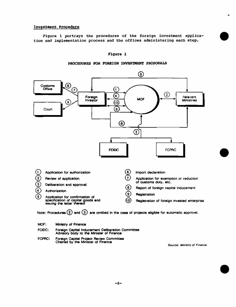
Investment Procedure
Figure 1 portrays the procedures of the foreign investment application and implementation process and the offices administering each step.
Figure 1
PROCEDURES FOR FOREIGN INVESTMENT PROPOSALS
( ^ Application for authorization
{2j Review of application
(3J Deliberation and approval
( 4 / Authorization
{SJ Application for confirmation of specification of capital goods and issuing the letter thereof
(&) Import declaration
KjJ Application for exemption or reduction of customs duty, etc.
B) Report of foreign capital Inducement
( 9 ) Registration
QO) Registration of foreign invested enterprise
Note: Procedures'^ and ( ^ are omitted in the case of projects eligible for automatic approval.
MOF: Ministry of Finance
FCIDC: Foreign Capital Inducement Deliberation Committee Advisory body to the Minister of Finance
FCPRC: Foreign Capital Project Review Committee Chaired by the Minister of Finance
Source: Ministry of Finance
- 6 -
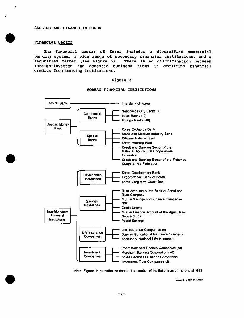
BANKING AND FINANCE IN KOR3BA
Financial Sector
The financial sector of Korea includes a diversified commercial banking system, a wide range of secondary financial institutions, and a securities market (see Figure 2) . There is no discrimination between foreign-invested and domestic business firms in acquiring financial credits from banking institutions.
Figure 2
KOREAN FINANCIAL INSTITUTIONS
Central Bank
Deposit Money Bank
Commefcia! Banks
N on-Monetary Financial
Institutions
Development Institutions
Savings Institutions
Life Insurance Companies
Investment Companies
The Bank of Korea
Nationwide City Banks (7) Local Banks (10) Foreign Banks (48)
Korea Exctiange Bank Small and Medium Industry Bank Citizens National Bank Korea Housing Bank Credit and Banking Sector of the National Agricultural Cooperatives Federation Credit and Banking Sector of the Fisheries Cooperatives Federation
Korea Development Bank Export-Import Bank of Korea Korea Long-term Credit Bank
Trust Accounts of the Bank of Seoul and Trust Company Mutual Savings and Finance Companies (191)
Credit Unions Mutual Finance Account of the Agricultural Cooperatives Postal Savings
Life Insurance Companies (5) Daehan Educational Insurance Company Account of National Life Insurance
Investment and Finance Companies (19) Merchant Banking Corporations (6) Korea Securities Finance Corporation Investment Trust Companies (2)
Note: Figures in parentheses denote the number of institutions as of the end of 1983
Source: BanI< of Korea
- 7 -
Small and Medium-Size Industry Support Organizations
In addition to the financial sector, there are many government and private institutions and organizations that support small and medium-size companies in every aspect of business, including start-up financing and the funding of new product development. Listed below are some of the most commonly used institutions for supporting small and medium-size companies:
• Banking Institutions
•T. The Korea Exchange Bank Address: 181 2-ka, Ulchi-ro, Choong-ku, Seoul, Korea Tel: 771-46
This is the largest commercial bank in Korea specializing in foreign exchange transactions, trade financing, and all areas of international banking. It maintains an international network of 38 branches, subsidiaries, and representatives.
•- The Small and Medium Industry Bank Address: 26-1 2-ka, Ulchi-ro, Choong-ku, Seoul, Korea Tel: 771-50
This bank supports all phases of banking needs for small and medium-size industries, including start-up financing.
The Citizen's National Bank Address: 9-1 2-ka, Namdaemoon-ro, Choong-ku, Seoul, Korea Tel: 771-40
This bank provides general banking with short-term loans to individuals and small companies. It gives special assistance to start-up companies with new products or technologies by providing long-term loans or equity investments.
— The Korea Long-term Credit Bank Address: 15-22 Yoido-dong, Youngdungpo-ku, Seoul, Korea Tel: 783-4431
This bank supports the commercialization of new technologies by providing long-term loans or equity investments.
• Venture Capital Companies
There are four private venture capital companies in Korea. However, they are heavily subsidized by the government and their objective is not primarily a high return to their investors. Their profits are mainly put into a revolving fund to support further investments with nominal dividends provided to the investors, who are usually public and private institutions. In addition to financial support, all of these venture capital companies provide services such as arranging private investment.
-8-
preparing business proposals, handling all of the procedures of business formation, and giving advice on managing the business. These venture capital companies can be of great assistance to foreign investors who wish to do business under a joint ventureship.
Korea Technology Development Corporation (KTDC) Address: 9th Fl., FKI Building
28-1 Yoido-dong, Youngdungpo-ku, Seoul, Korea Tel: 783-7601, 783-7851
KTDC was established in 1977 under the "Korea Technology Development Act" that provides government support with autonomous, private management. It provides funds to business enterprises at favorable terms, including equity investments needed for developing technology. In most cases it provides up to $1 million a year to a large number of companies.
Korea Development Investment Corporation (KDIC) Address: 12th Fl., Private School Endowment Building
27-2 Yoido-dong, Youngdungpo-ku, Seoul, Korea Tel: 783-9574
KDIC was established in 1982 by domestic and international investment companies. It is very selective, but provides large amounts of money, depending on the project. It is similar in character to U.S. venture firms. Its primary investment is in new inventions or technologies either from domestic or foreign businesses manufacturing in Korea.
<- Korea Technology Financing Corporation (KTFC) Address: Industrial Bank Building
10-2 Kwanchul-dong, Chongro-ku, Seoul, Korea Tel: 744-5411
KTIC is sponsored by domestic private financial institutions. It is similar to the KTDC.
- Korea Technology Advancement Corporation (K-TAC) Address: c/o KAIST
39-1 Hawolgok-dong, Sungbook-ku, Seoul, Korea Tel: 962-8197
K-TAC was established by seven government R&D organizations to commercialize their technological developments. In addition, several domestic banking and investment organizations support the venture. The company also provides funds to those with technologies from sources Other than their member R&D firms.
-9-
THE BOTTOM LINE
The FCIA guarantees the overseas remittance of profit dividends accruing from the stock or shares acquired by a foreign investor, sales proceeds from stock or shares, principal, interest and fees to be paid under a loan contract or a public loan agreement, and royalties to be paid under a technology inducement contract. When a foreign investor wants to remit abroad, one must file an application with the president of the Foreign Exchange Bank (such as the Korea Exchange Bank) for approval. The president of the bank will approve the application after reviewing the legitimacy of the repatriation.
Should a foreign investor want to invest profit dividends accruing from the stock or shares acquired in accordance with the FCIA in an enterprise in Korea, the investor must report to the Minister of Finance and first obtain approval. Then all properties of foreign-invested enterprise are guaranteed and protected from requisition or expropriation under pertinent laws and decrees.
CONCLDSIONS
It is Dataquest's opinion that there will be many new joint venture companies formed between U.S. and Korean investors in the next five years. Specifically, we see the semiconductor industry growing at a compound annual growth rate of a minimum of 22 percent over the next five years, and with this high rate, local companies will be funded to support its growth.
Gene Norrett Dr. Mike Bae
-10-
DataQuest :i tomuanv ot Thi'tltinKiinicisl ttei Cnrpnra) tan
JAPANESE RESEARCH
NEWSLETTER
JSIS Code: Newsletters 1985-1986, JSIA 1986-29
SEMICONDUCTOR APPLICATIONS: SECOND QUARTER UPDATE
INTRODUCTION
Because of the need for detailed semiconductor application information, DATAQUEST's Japanese Semiconductor Industry Service (JSIS) will issue a quarterly newsletter addressing detailed equipment trends, semiconductor application data, and analysis. This issue marks our first such newsletter. We have chosen to summarize 1985 end-equipment trends in Japan and to examine VTRs in particular.
SUMMARY
Equipment production value in Japan was $69.3 billion in 1985 and semiconductors worth $8.6 billion were consumed. DATAQUEST's JSIS compiled data about semiconductor consumption in Japan and completed our analysis as follows:
• Japanese equipment production value increased from $59.5 billion in 1984 to $69.3 billion in 1985, achieving 16.5 percent growth. So as to show the real growth in production we have presented the figures in yen in Figure 1 and in dollars in Table 1.
• Semiconductor consumption decreased by 2.3 percent, $8.8 billion in 1984 to $8.6 billion in 1985.
from
1986 Dataquest Incorporated June—Reproduction Prohibited
The content of this report represents our interpretation and analysis of inlormalion generally available to the public or released by responsible individuals in the subject companies, but is not guaranteed as to accuracy or completeness It does not contain material provided to us in confidence by our clients Individual companies reported on and analyzed by DATAQUEST, may be clients o( this and/or other DATAQUEST services This information is not furnished in connection with a sale or offer to sell securities or in connection with the solicitation ot an offer lo buy securities This firm and its parent and/or their officers, stockholders, or members ol their families may, from time lo time, have a long or short position in the securities mentioned and may sell or buy such securities
Taiyo Ginza Building / 7-14-16 Ginza, Chuo-ku / Tokyo 104, Japan / (03) 546-3191 / Telex J32768 1290 Ridder Park Drive / San Jose, CA 95131-2398 / (408) 971-9000 / Telex 171973
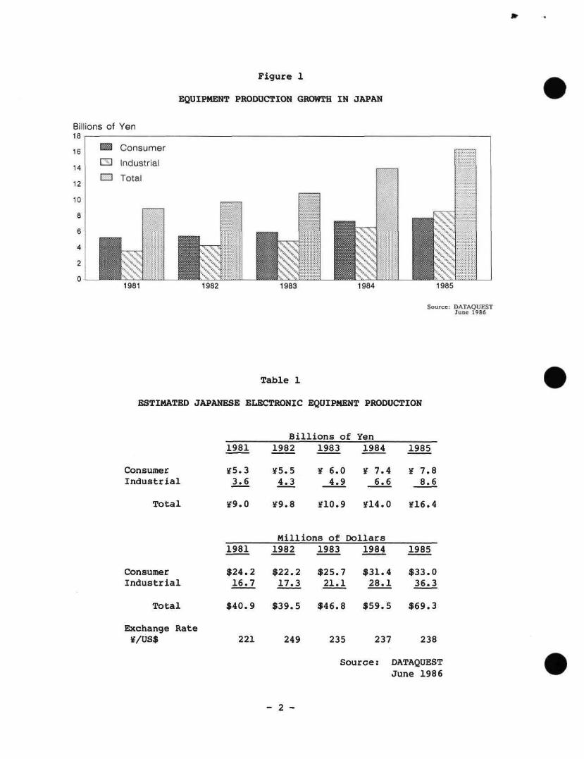
Figure 1
EQUIPMENT PRODUCTION GROWTH IN JAPAN
Bil 18
16
14
12
10
8
6
4
2
0
ions of Yen
M Consunner
[ 3 Industrial
WM Total
1981 1982 1983 1984 1985
Source: DATAQUEST June 19S£
Table 1
ESTIMATED JAPANESE ELECTRONIC EQUIPMENT PRODUCTION
Consumer Industrial
Total ¥9.0
Billions of Yen 1981
¥5.3 3 .
1982
¥5.5 4.3
1983
¥ 6.0 4.9
1984
¥ 7.4 6.6
1985
¥ 7.8 8.6
¥9 .8 ¥10 .9 ¥14 .0 ¥16.4
Consumer Industrial
Total
Exchange Rate ¥/US$
1981
$24.2 16.7
221
Millions of Dollars 1982
$22.2 17.3
1983 1984
$25.7 $31.4 21.1 28.1
249 235 237
1985
$33.0 36.3
$40.9 $39.5 $46.8 $59.5 $69.3
238
Sou r c e: DATAQUEST June 1986
- 2 -
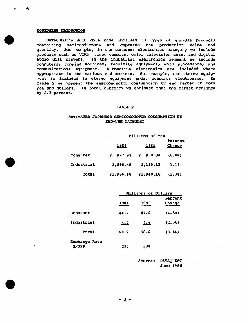
EQUIPMENT PRODUCTION
DATAQUEST's JSIS data base includes 50 types of end-use products containing semiconductors and captures the production value and quantity. For example, in the consumer electronics category we include products such as VTRs, video cameras, color television sets, and digital audio disk players. In the industrial electronics segment we include computers, copying machines, facsimile equipment, word processors, and communications equipment. Automotive electronics are included where appropriate in the various end markets. For example, car stereo equipment is included in stereo equipment under consumer electronics. In Table 2 we present the semiconductor consumption by end market in both yen and dollars. In local currency we estimate that the market declined by 2.3 percent.
Table 2
ESTIMATED JAPANESE SEMICONDUCTOR CONSUMPTION BY END-USE CATEGORY
Billions of Yen
1984 1985 Percent Change
Consumer ¥ 997.92 ¥ 938.04 (6.0%)
Industrial 1,098.48 1,110.12 1.1%
Total ¥2,096.40 ¥2,048.16 (2.3%)
Millions of Dollars
Consumer
Industrial
Total
Exchange Rate ¥/US$
1984
$4.2
4.7
$8.9
237
1985
$4.0
4.6
$8.6
238
Percent Change
(4.8%)
(2.0%)
(3.4%)
Source; DATAQUEST June 1986
- 3 -
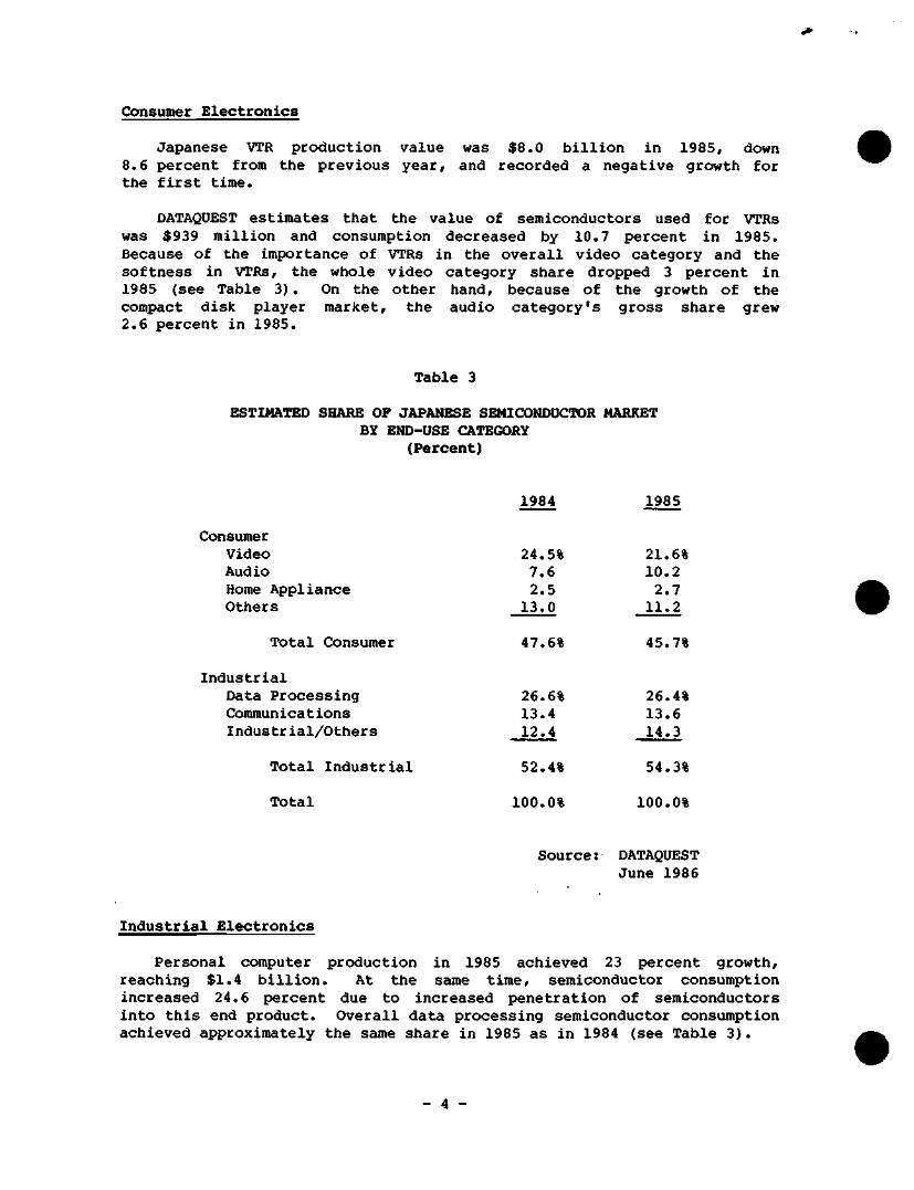
Consumer Electronics
Japanese VTR production value was $8.0 billion in 1985, down 8.6 percent from the previous year, and recorded a negative growth for the first time.
DATAQUEST estimates that the value of semiconductors used for VTRs was $939 million and consumption decreased by 10.7 percent in 1985. Because of the importance of VTRs in the overall video category and the softness in VTRs, the whole video category share dropped 3 percent in 1985 (see Table 3) . On the other hand, because of the growth of the compact disk player market, the audio category's gross share grew 2.6 percent in 1985.
Table 3
ESTIMATED SHARE OF JAPANESE SEMICONDUCTOR MARKET BY END-USE CATEGORY
(Percent)
1984 1985
Consumer Video Audio Home Appliance Others
24.5% 7.6 2.5 13.0
21.6% 10.2 2.7 11.2
Total Consumer 47.6% 45.7%
Industrial Data Processing Communications Industrial/Others
Total Industrial
Total
26.6% 13.4 12.4
52.4%
100.0%
Source:
26.4% 13.6 14.3
54.3%
100.0%
DATAQUEST June 1986
Industrial Electronics
Personal computer production in 1985 achieved 23 percent growth, reaching $1.4 billion. At the same time, semiconductor consumption increased 24.6 percent due to increased penetration of semiconductors into this end product. Overall data processing semiconductor consumption achieved approximately the same share in 1985 as in 1984 (see Table 3).
- 4 -
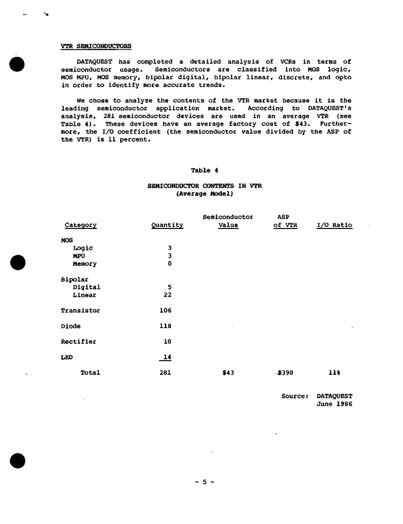
VTR SEMICONOaCTORS
DATAQUEST has completed a detailed analysis of VCRs in terms of semiconductor usage. Semiconductors are classified into MOS logic, MOS MPU, MOS memory, bipolar digital, bipolar linear, discrete, and opto in order to identify more accurate trends.
We chose to analyze the contents of the VTR market because it is the leading semiconductor application market. According to DATAQUEST's analysis, 281 semiconductor devices are used in an average VTR (see Table 4). These devices have an average factory cost of $43. Furthermore, the I/O coefficient (the semiconductor value divided by the ASP of the VTR) is 11 percent.
Table 4
SEMICONDUCTOR CONTENTS IN VTR (Average Model)
Category
MOS Logic MPU Memory
Bipolar Digital Linear
Transistor
Diode
Rectifier
LED
Total
Quantity
3 3 0
5 22
106
118
10
14
281
Semiconductor Value
$43
ASP Of VTR
$390
I/O Ratio
11%
Source: DATAQUEST June 1986
- 5 -
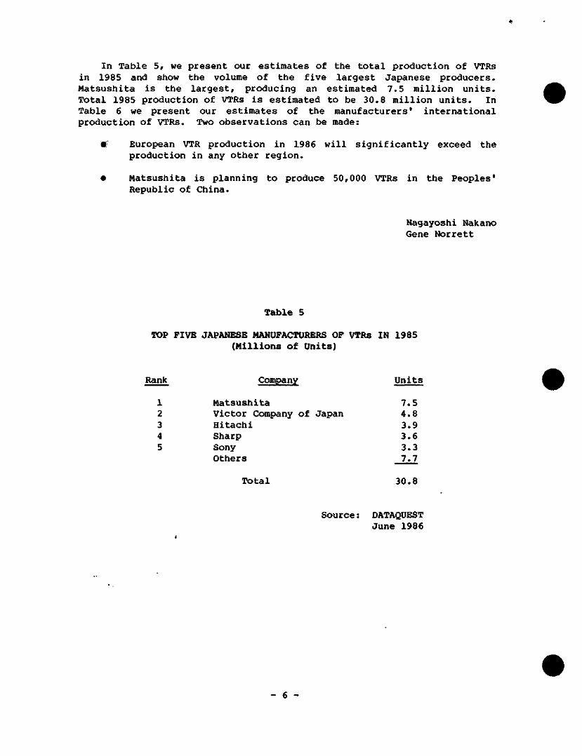
In Table 5, we present our estimates of the total production of VTRs in 1985 and show the volume of the five largest Japanese producers. Matsushita is the largest, producing an estimated 7.5 million units. Total 1985 production of VTRs is estimated to be 30.8 million units. In Table 6 we present our estimates of the manufacturers' international production of VTRs. Two observations can be made:
• European VTR production in 1986 will significantly exceed the production in any other region.
• Matsushita is planning to produce 50,000 VTRs in the Peoples' Republic of China.
Nagayoshi Nakano Gene Norrett
Table 5
TOP FIVE JAPANESE MANUFACTURERS OF VTRs IN 1985 (Millions Of Units)
Rank Company Units
1 2 3 4 5
Matsustiita Victor Company of Japan Hitachi Sharp Sony Others
7.5 4.8 3.9 3.6 3.3 7.7
Total 30.8
Source: DATAQUEST June 1986
- 6 -
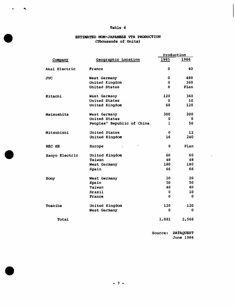
Table 6
ESTIMATED NON-JAPANESE VTR PRODUCTION (Ttiousands of Units)
Production Company
Akai Electric
JVC
Hitachi
Matsushita
Mitsubishi
NEC HE
Sanyo Electric
Sony
Toshiba
Geographic Location
France
West Germany United Kingdom United States
West Germany United States United Kingdom
West Germany United States Peoples' Republic of China
United States United Kingdom
Europe
United Kingdom Taiwan West Germany Spain
West Germany Spain Taiwan Brazil France
United Kingdom West Germany
1985 1986
40
0 0 0
120 0 60
300 0 1
0 16
480 360 Plan
360 10 120
300 0 50
12 240
Plan
60 48 180 66
20 50 40 0 0
120 0
60 48 180 66
20 50 40 10 0
120 0
Total 1,081 2,566
Source: DATAQUEST June 1986
- 7 -
Dataquest JUC Dun & Bi;»ttstftct COT poratimi
JAPANESE RESEARCH
NEWSLETTER
JSIS Code: Newsletters 1985-1986, JSIA 1986-30
JAPANESE MICRODEVICE INDUSTRY UPDATE— HIGH-PERFORMANCE CMOS TECHNOLOGY IS DRIVING FORCE
INTRODUCTION
Microcomputer Show '86 was held in Tokyo, Japan, in late May. This was the tenth year for this show, organized by the Japanese Electronics Industry Development Association (JEIDA). The participants, which included major Japanese semiconductor manufacturers, showed many new products.
The exhibits at the show made it apparent to DATAQUEST that high-performance CMOS technology is the driving force for new products.
MARKET OVERVIEW
In 1985, Japanese microdevice production declined by 4 percent from the previous year, due to the weak demand by the video cassette recorder (VCR) and personal computer (PC) markets. However, DATAQUEST estimates that this year's growth rate will be high for the following reasons:
• IBM announced a new laptop PC that uses a CMOS MPU (80C88) and memories. CMOS is one of the Japanese semiconductor industry's strong areas.
• Japan has a lion's share of the world consumer electronics market, which is becoming increasingly semiconductor-intensive (due to such products as 8mm VCRs and portable televisions) , and, therefore, increasing the consumption of CMOS products.
• In the technology areas, CMOS micro is a powerful negotiation tool for several Japanese companies to establish market leadership with products such as NEC's CMOS V series and Hitachi's high-performance CMOS 6301 8-bit MCU.
1986 Dataquest Incorporated June—Reproduction Prohibited
\
The content of this report represents our interpretation and analysis of intormation generally available to the public or released by responsible individuals in the subject companies, but is not guaranteed as to accuracy or completeness II does not contain material provided to us in contidence by our clients Individual companies reported on and analyzed by DATAQUEST, may be clients of this and/or other DATAQUEST services This informalion is not furnished in connection with a sale or offer to sell secunties or in connection with the solicitation ol an otter lo buy securities This firm and its parent and/or their officers, stockhoiders, or members ot their families may, from time to lime, have a long of short position in the secunties mentioned and may sell or buy such secunties
Taiyo Ginza Building / 7-14-16 Ginza, Chuo-ku / Tokyo 104, Japan / (03) 546-3191 / Telex J32768 1290 Bidder Park Drive / San Jose, CA 95131-2398 / (408) 971-9000 / Telex 171973
NEW CMOS MPU/MCU/MPR PRODUCTS IN MICROCOMPUTER SHOW '86
At the show, many companies introduced new products (see Table 1) • DATAQUEST has observed the following trends among these new products:
• Original design MPUs, such as NEC's V60 (16-bit), Matsushita's MN1617 (16-bit), and Mitsubishi's M63162 (16-bit.) The V60 has very high performance (5 MIPS) and impressive architecture such as vertical storage, on-chip floating-point calculation function, and pipelined hardware. Ttie V60 process technology, with 1.5-micron design rule and 2-layer aluminum circuit, can realize about 375,000 transistors on-chip. Matsushita's MN1617, jointly developed by Matsushita Electronics Corporation and Matsushita Electric Industrial Co., Ltd., is an enhanced version of the MN1613. This high-speed MPU operates at 20 MHz, can address 4 Mbytes of main memory, uses a 2-micron CMOS process with single poly and double-layer aluminum technology, and contains 60,500 transistors on a 6.7mm x 7.0mm chip. Mitsubishi's M63162 has an original design with three levels of pipelined control architecture and uses 2-micron design rule with polycide gate and 2-layer aluminum technology. The chip size is 9.26 x 7.50mm, and contains about 59,000 transistors.
• CMOS versions of existing popular NMOS products, such as Hitachi's HD68HC000 and Fujitsu's Intel-compatible MPRs. DATAQUEST estimates that these CMOS products will be major components for future advanced and very smart office equipment.
• Specific MPRs for the Japanese market for FAX and CAPTAIN (VIDEOTEX). Hitachi's HD63084/HD63085y has been developed for G3/G4 high-speed facsimile machines. Fujitsu's MB 89323/324 is a multiplex character controller for the CAPTAIN system, and has analog RGB (red, green, blue) outputs and 12 Mbytes of RAM addressing capability.
DATAQUEST ANALYSIS
The world electronic equipment production by major regions is changing now because of lower costs, government promotion, and technology development. As a result of the current changes, we expect the Asian region to become the major production site, not only for consumer equipment, but also for low-cost computer-related products, including PCs. However, the Japanese industry is experiencing hard times because of the high yen. The Japanese semiconductor industry has been hurt by price pressure coming from domestic customers who have had to reduce their costs to maintain their competitive power against the yen increase. Furthermore, trade friction is causing various other pressures against Japanese manufacturers.
- 2 -
J
Under the circumstances, DATAQUEST believes that the high-performance CMOS microdevices will be a driving force in developing the new demand that is increasing in domestic and foreign markets. We believe that CMOS micros will pull up the Japanese industry to a leadership position in micros in light of the following observations:
• The Japanese manufacturers dominate the high-performance CMOS processes, especially high-geometry processes such as the sub-2-micron area.
• Using strong process technology, there are two directions for new product developmeilt to take. One direction is to convert all NMOS devices to CMOS. In this case, the suppliers can increase orders immediately. Another direction is to develop original products to develop new markets.
• We expect high-performance CMOS technology to become the major process for products such as 1Mb DRAMs, 4Mb DRAMs, and micros; this trend means that there is an opportunity for the Japanese to gain leadership not only in micros, but in all semiconductor business.
Osamu Ohtake
- 3 -
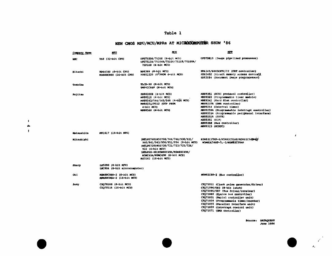
Table 1
CMOS MPU/MCU/MPRs AT MICRO©OHlKl!fiSiR SHOW ' 8 6
CoMpany H une
NSC
Hi tach i
TosAiba
Fu j i tmi
MPU
V60 ( 3 2 - b i t CPU)
11064180 ( 8 - b l t CPU) ROeSHCOOO ( 1 6 - b l t CPO)
I
*>. I
Matsush i ta
Mi t sub i sh i
mien (is-bit HPU)
MCU
[1PO75206/7520B ( 4 - b l t KCIJ) tJPD75101/75104A/7Si06/75108/75108A/
7SP10fl « - b i e HCU)
BQG309 {8-b l t HCZU] MW01220 (E^PftOH <-t)it («0)
TLCS-90 ( 8 - b i t HCUt TMP-CCeeP (<-tJit MCU)
flfl8a200B « - b i t HCU) BBSasiO j 4 - b i t HCU) Hfi68543/544/5<V5<6 (4- tS« MCO) MBe8S51/P552 (OTP PROM
4 - b i t MCU) HBiSbSO ( 4 - b i t MCU)
(MELPS740)M50708/744/746/930/931/ 940/941/943/950/951/954 ( 8 - b i t MCO)
(MELPS720)H50720/721/723/725/726/ 922 ( 4 - b i t MCU)
(MELPS8-48)M5H80C49A/H5HS0C49R/ M5MC49A/M5MC49H ( 8 - b i t MCO)
Me3162 ( 1 6 - b i t MCO)
KPR
0PD7281D (image pipelined procesBor)
HD6345/6445CRTC/ri (CRT COntcoller) HDfi3450 (Direct mEiKiry access control) BDG30B4 (Docunent laiage pEsprocessor}
Ma89351 (SCSI protocol controller) HeB9362 (Progtamable tiner nodule) MB89341 (Rard disk controlleil MB89237A (DMA controller) HB89254 (Interval tlnerl MB89259A (Progranmable interrupt controller) MAB9255A (PrograiuHble peripheral interface) MB89251A (5DTR) HfiS9391 (SIP) MaB92Ba (Bus controller) HBfl9323 (HCRTC)
M5MS 2C 3 7A P - 4 / H 5M fl 2CS lAP/HSHB 2C 5 4 ( H ( / M5«a 2C 5 4 AP-5 , - 2/KSHB 2C5 9A P
Sharp
Oki
Sony
UI508Q ( 8 - b i t HPO) UlCSOa ( 8 - b i t microGonputer)
MSMS0C88A-2 ( 8 - b i t MCO) mH80CS6A-2 {16-bi t MCO)
CXQ70108 (8-bit MCO) CXQ70116 (16-bit MCO)
MSM82C88-2 (Bus oontroUer)
CXQ71011 (clocIi pulse generator/diiver) C)C(}71096/Oe3 (B-bit latch) CX(}71086/oa7 (BUB driver/receiver) CXQ7108B (Syaten bus controller) CXQ71051 (Serial controller unit) CXQ71054 (PrograiMitable timer/counter) CXQ710S5 (Parallel Interface unit) CXQ71059 (Interrupt control unit) C31071071 {DMA controller)
Source: DATAQOSSr June 1986
DataQuest ;i cumpGnv u1 T he rKin & B radst re cU OC[KH;)1 ion
JAPANESE RESEARCH
NEWSLETTER
JSIS Code: Newsletters 1985-1986, 1986-28
JSIA
JAPANESE CAPTIVE SEMICONDUCTOR SALES: AN OVERVIEW
SUMMARY
DATAQUEST recently completed its first survey of captive sales by the major Japanese semiconductor manufacturers. It has long been recognized that semiconductors account for only a small portion of total sales for the largest suppliers, such as NEC, Hitachi, Toshiba, and Fujitsu. Most of these semiconductor operations were begun to supply in-house needs, and evolved into merchant supply over time.
DATAQUEST"s market estimates and market share data have always included both merchant and captive sales by companies that sell to the merchant market. Because of the heavy Japanese dependence on captive semiconductor supply, foreign suppliers (U.S., European, and ROW) have a need to know what portion of the Japanese market is actually available for merchant sales. When a Japanese company supplies a closely associated company (for example, the same banking group), it is not considered captive in this data.
It is our intention to update this survey on an annual basis. Currently, research is proceeding on a similar study of U.S. and European semiconductor suppliers; we will publish those results upon completion of data collection and analysis.
CAPTIVE SALES BY MANUFACTURER
Table 1 lists the captive and total semiconductor sales of the top nine Japanese semiconductor manufacturers from 1981 through 1985. Matsushita and Sanyo, two large consumer electronics companies, are the most heavily captive of the top nine. We estimate Matsushita's captive portion at 50 percent in 1985, and Sanyo's at 24 percent. Figure 1 shows captive sales versus total semiconductor sales for each of the top nine companies in 1985.
1986 Dataquest Incorporated June—Reproduction Prohibited
The content of this report represents our interpretation and analysis of information generally available to the public of released by responsible individuals in the subject companies, but is no\ guaranteed as to accuracy or completeness It does not contain material provided to us in confidence by our clients Individual companies reported on and analyzed by DATAQUEST, may be clients of this and/or other DATAQUEST services This information is not furnished in connection with a sale or offer to sell securities Of in connection with the solicitation of an offer to txjy securities This firm and its parent and/or their officers, stockholders, or members of their families may, from time to time, have a long or short position in the securities mentioned and may sell or buy such securities
Taiyo Ginza Building / 7-14-16 Ginza, Chuo-l<u / Tokyo 104, Japan / (03) 546-3191 / Telex J32768 1290 Ridder Park Drive / San Jose, CA 95131-2398 / (408) 971-9000 / Telex 171973
The average captive percentage for the top nine companies was 22 percent in 1985, down slightly from 23 percent in 1981. In general, captive sales rise as a percentage of total sales during a year of slow growth or recession, and fall during a year of rapid growth, such as 1984. In 1984, captive sales represented only 19 percent of the top nine companies' total semiconductor sales.
Among the companies included in our "Others" category are Fuji, Ricoh, Rohm, Sanken Electric, Seiko-Epson, and Sony. These companies accounted for only 13 percent of all Japanese company revenue, but they accounted for 25 percent of all Japanese captive sales.
As shown in Figure 2, captive sales declined very slightly in absolute value in 1985, but increased as a percentage of total semiconductor sales. In 1982, captive sales were also slightly down, but total semiconductor sales increased 3 percent; thus, the captive percentage decreased three percentage points. Captive sales stood at 30 percent of total sales in 1981. They reached a low point in 1984, at 22 percent, and rose in 1985 to 25 percent.
CAPTIVE PORTION OF THE MARKET
We estimate the captive portion of the Japanese semiconductor market to have been 30 percent in 1985, up from 29 percent in 1984, but down from 33 percent in 1981. We believe that almost all captive semiconductor sales by Japanese companies are in Japan; therefore, these percentages are calculated by dividing total Japanese company captive sales by the size of the Japanese semiconductor market. This is shown graphically in Figure 3.
Patricia S. Cox Nagayoshi Nakano Osamu Ohtake
- 2 -
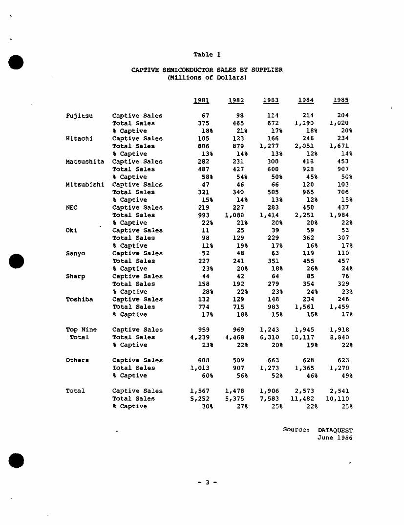
Table 1
CAPTIVE SEMICONDUCTOR SALES BY SUPPLIER (Millions o£ Dollars)
1981 1982 1983 1984 1985
Fujitsu
Hitachi
Matsushita
Mitsubishi
NEC
Oki
Sanyo
Sharp
Toshiba
Top Nine Total
Others
Total
Captive Sales Total Sales % Captive Captive Sales Total Sales % Captive Captive Sales Total Sales % Captive Captive Sales Total Sales % Captive Captive Sales Total Sales % Captive Captive Sales Total Sales % Captive Captive Sales Total Sales % Captive Captive Sales Total Sales % Captive Captive Sales Total Sales % Captive
Captive Sales Total Sales % Captive
Captive Sales Total Sales % Captive
Captive Sales Total Sales % Captive
67 375 18%
105 806 13%
282 487 58% 47 321 15%
219 993 22% 11 98 11% 52 227 23% 44
158 28%
132 774 17%
959 4,239
23%
608 1,013
60%
1,567 5,252
30%
98 465 21%
123 879 14% 231 427 54% 46
340 14% 227
1,080 21% 25
129 19% 48 241 20% 42
192 22%
129 715 18%
969 4,468
22%
509 907 56%
1,478 5,375
27%
1
1
1 6
1
1 7
114 672 17% 166 ,277 13%
300 600 50% 66
505 13% 283 ,414
20% 39
229 17% 63 351 18% 64
279 23%
148 983 15%
,243 ,310
20%
663 ,273
52%
,906 ,583
25%
1
2.
2
1
1 10
1
2 11
214 ,190 18% 246 ,051 12% 418 928 45% 120 965 12%
450 ,251 20% 59
362 16%
119 455 26% 85
354 24%
234 ,561 15%
,945 ,117
19%
628 ,365 46%
,573 ,482
22%
1,
1,
1
1
1 8
1
2 10
204 ,020 20% 234 ,671 14%
453 907 50% 103 706 15%
437 ,984
22% 53
307 17%
110 457 24% 76
329 23%
248 ,459 17%
,918 ,840
22%
623 ,270 49%
,541 ,110
25%
Source: DATAQUEST June 1986
- 3 -
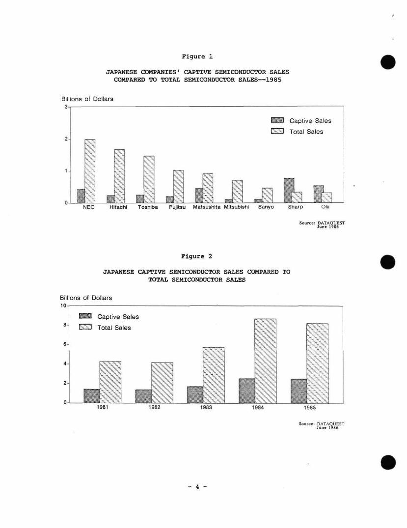
Figure 1
JAPANESE COMPANIES' CAPTIVE SEMICONDUCTOR SALES COMPARED TO TOTAL SEMICONDUCTOR SALES—1985
Billions of Dollars 3-
1- i I m
i -'.yX
I 1
I i A,
_ ^ V'-
Captive Sales
Total Sales
NEC Hitachi Toshiba Fujitsu Matsushita Mitsubishi Sanyo Sharp OI<i
Figure 2
JAPANESE CAPTIVE SEMICONDUCTOR SALES COMPARED TO TOTAL SEMICONDUCTOR SALES
Source: DATAQUEST June 1986
Billions of Dollars 10-
6.
^ ™ Captive Sales
ES ] Total Sales
1981 1982 1983 1984 1985
Source: DATAQtlESt June 19S6
- 4
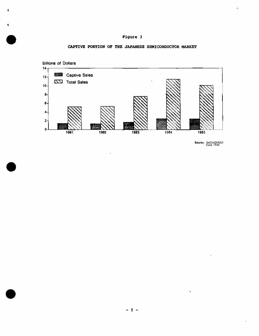
Figure 3
CAPTIVE PORTION OP THE JAPANESE SEMICONDUCTOR MARKET
Billions of Dollars 14-
12
10
ST.
6*
4^
2-
0
^M Captive Sales
E 3 Total Sales
sss> ^W % ^
'V^X.;:"i
^ss >s-\ ••'•»
1981 1982 1983 1984 19Q5
Source: DATAQUEST June 19S6
5 -
Dataquest jcQmpsnvul rhc nunSi''flrKl%i;rcct cnrporatitm
JAPANESE RESEARCH
NEWSLETTER JSIS Code: Newsletters 1985-1986, JSIA
1986-25
JAPANESE SEMICONDUCTOR MARKET QUARTERLY UPDATE: RIGHT ON COURSE
DATAQUEST has made only minor changes to its forecast for the Japanese semiconductor market since our February 11 newsletter. We still foresee moderate growth of 9.4 percent in yen. The wild card in this year's forecast is, of course, the sinking dollar. We have traditionally assumed constant exchange rates for our dollar forecasts; this year, we used the 1986 beginning exchange rate—203 yen per U.S. dollar— throughout 1986 and beyond.
However, the dollar has continued to fall, and has reached a low point of 160 yen per dollar. If this continues throughout the year, it will, of course, affect the dollar value of the Japanese semiconductor market. For instance, at 203 yen per dollar, 9.4 percent growth in yen would equal 28.3 percent growth in dollars; at 175 yen per dollar, dollar growth would be a whopping 48.8 percent.
The strength of the yen has already resulted in pricing pressure in Japan from semiconductor purchasers struggling to keep costs down so they can continue to price competitively in the U.S. market. On the other hand, U.S. semiconductor manufacturers are becoming much more competitive in the Japanese market.
We continue to forecast strong growth in 1987, with the Japanese semiconductor market growing 30.7 percent (both yen and dollars).
Tables 1 and 2 show our quarterly forecast and growth rates through 1987, in yen. Tables 3 and 4 show the same forecast calculated in U.S. dollars.
NOTE: Our complete forecast from 1986 through 1991, plus 1996, is in publication, and should arrive on each JSIS notebook holder's desk in early June.
Patricia S. Cox
© 1986 Dataquest Incorporated May—Reproduction Prohibited
The contenl of this report represents our interprelatIon and analysis ot information generally available to the publIc or released by responsible individuals in the subject companies, but is no! guaranteed as to accuracy or completeness It does nol contain material provided lo us in contidence by our clients Individual companies reported on and analyzed by DATAQUEST, may be clients of this and/or other DATAQUEST services This information is not furnished In connection with a sale or offer lo sell securities or In connection with the solicitation o1 an offer to buy securities This firm and its parent and/or their officers, stockholders, or members of their lamilies may, from time to time, have a long or short position in the securities mentioned and may sell or buy such securities
Taiyo Ginza Building / 7-14-16 Ginza, Chuo-ku / Tokyo 104, Japan / (03) 546-3191 / Telex J32768 1290 Ridder Park Drive / San Jose, CA 95131-2398 / (408) 971-9000 / Telex 171973
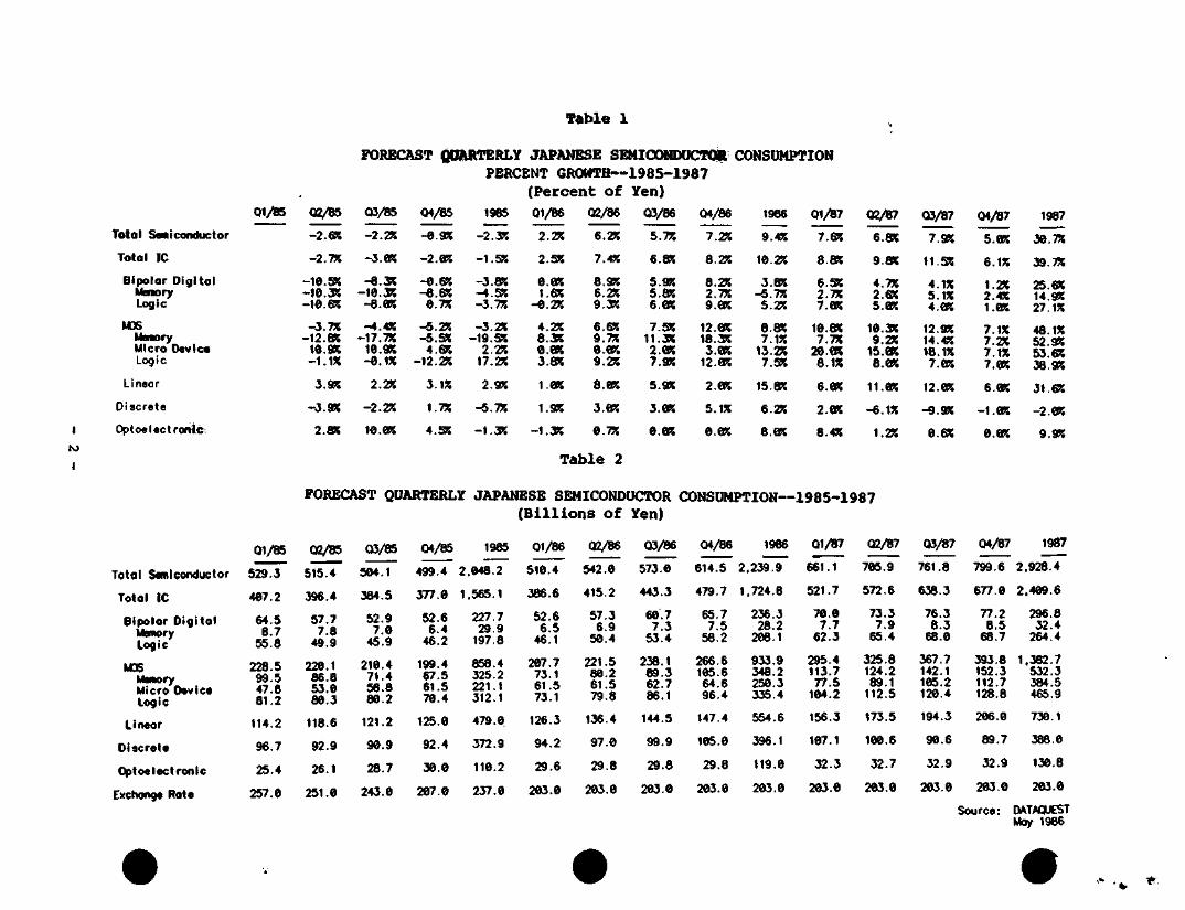
Table 1
FORECAST QDHRTERLY JAPANESE SEMICONDUCTOR CONSUMPTION PERCENT GROWTH—1985-1987
(Percent of Yen)
1
to
1
01/85 Q /B5
Total Smiconductor
Total JC
Bipolar Digital Memory Logic
MDS Umory Micro Device Logic
Linear
Discrete
Optoelectronfi.ci
-2.eK
-2.7%
-10.5K -10.3J! -10.6%
-3.7% -12.8%
10.9% -1 .1%
3.9%
-3.9%
2.8%
03/85
-2.2%
-3.C%
-a.3% -10.3% -B.0%
-4 .«5 -17.7%
10.S% -«.1%
2.2%
-2.2%
io.e%
04/85
-0.9%
-2.6%
-«.6% -8.6% 0.7%
-5.2% -5.5%
4.6% -12.2%
3.1%
1.7%
4.S%
1985
-2.3J!
-1.5%
-3.8% -4.5% -3.7%
-3.2% -19.5%
2.2% 17.2%
2.9%
-5.7%
-1.3%
01/86
2.2%
2.5%
o.e% 1.6%
-«.2%
4.2% 8.3% e.e% 3.8%
1.0%
1.9%
-1.3%
02/86
6.2%
7.4%
8.9% 6.2% 9.3%
6.6% 9.7% O.CR 9.2%
8.e%
3.6%
0.7%
Table 2
03/86
5.7%
6.8%
5.9% 5.8% 6.6%
7.5% 11.:3% 2.0% 7.9%
5.9%
3.6%
0.6%
04/86
7.2%
8.2%
8.2% 2.7% 9.6%
12.6% 18.3% 3.6%
12.e%
2.6%
5.1%
0.0%
1986
9.4%
10.2%
3.8% -5.7% 5.2%
8.8% 7.1%
13.2% 7.5%
15.8%
6.2%
8.6%
01/87
7.6%
8.8%
6.5% 2.7% 7.6%
10.8% 7.7%
20.6% 8.1%
6.6%
2.6%
8 . « :
02/87
6.8%
9.8%
4.7% 2.6% 5.6%
10.3% 9.2%
15.6% 8.6%
11.0%
-6 .1%
1.2%
03/87
7.9%
11.5%
4.1% 5.1% 4.6%
12.9% 14 .«: 18.1% 7.6%
12.6%
-9.9%
0.6%
04/87
5.6%
6.1%
1.2% 2 . ^ 1.6%
7.1% 7.2% 7.1% 7.6%
6.6%
-1.6%
0.6%
1987
30.7%
39.7%
25.6% 14.9% 27.1%
48.1% 52.SK 53.6% 38.9%
31.6%
-2.8%
9.9%
FORECAST QUARTERLY JAPANESE SEMICONDUCTOR (Billions of Yen)
CONSOMPTION~1985-1987
01/85 02/85
Total Semiconductor 529.3 515.4
Total IC 407.2 396.4
Bipolar Digital 64.5 57.7 MOTory 8.7 7.8 Logic 55.8 49.9
U S 228.5 220.1 Memory 99.5 86.8 Micro Device 47.8 53.0 Logic 81.2 80.3
Lirtear 114.2 118.6
Diacrete 96.7 92.9
Optoelectronic 25.4 26.1
E>cchong« Rate 257.0 251.0
03/85 04/85
504.1
384.5
52.9 7.0 45.9
210.4 71.4 56.8 80.2
121.2
90.9
28.7
243.0
499.4 2
377.0 1
52.6 6.4 46.2
199.4 67.5 61.5 70.4
125.0
92.4
30.0
207.0
1985
.048.2
.565.1
227.7 29.9 197.8
858.4 325.2 221.1 312.1
479.0
372.9
110.2
237.0
01/86 02/86 03/86
510.4
386.6
52.6 6.5 46.1
207.7 73.1 61.5 73.1
126.3
94.2
29.6
203.0
542.0
415.2
57.3 6.9 50.4
221.5 80.2 61.5 79.8
136.4
97.0
29.8
203.0
573.0
443.3
60.7 7.3 53.4
238.1 89.3 62.7 86.1
144.5
99.9
29.8
203.0
04/86
614.5 2,
479.7 1,
65.7 7.5 58.2
266.6 105.6 64.6 96.4
147.4
105.0
29.8
203.0
1986
239.9
724.8
236.3 28.2 208.1
933.9 348.2 250.3 335.4
554.6
396.1
119.0
203.0
01/87
661.1
521.7
70.0 7.7 62.3
295.4 113.7 77.5 104.2
156.3
107.1
32.3
203.0
02/87
705.9
572.6
73.3 7.9 65.4
325.8 124.2 ra.1 112.5
173.5
100.6
32.7
203.0
03/87 04/87 1987
761.8 799.6 2.928.4
638.3 677.0 2.409.6
76.3 8.3 68.0
367.7 142.1 105.2 120.4
194.3
90.6
32.9
203.0
77.2 8.5
68.7 393.8 152.3 112.7 128.8
206.0
89.7
32.9
203.0
Source
296.8 32.4 264.4
1.382.7 532.3 384.5 465.9
730.1
388.0
130.8
203.0
DATAQUEST May 1986
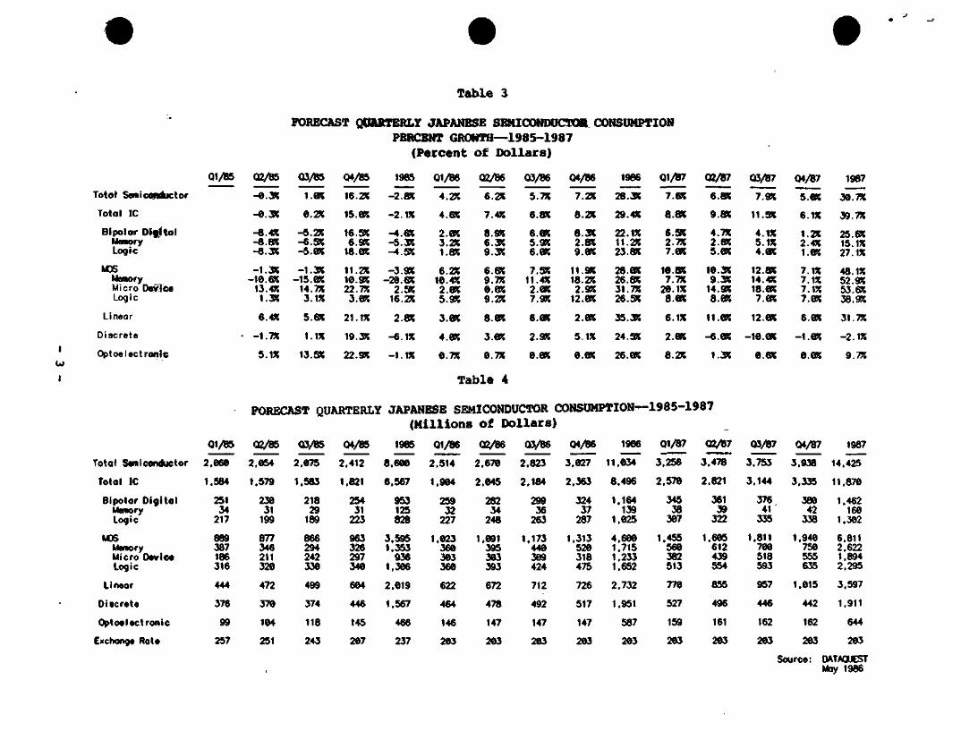
Table 3
FORECAST QtnRTERLY JAPANESE SEHICOHDUCTOS CONSWIPTION
I CJ
I
Totot Semiconductor
Totol IC
Bipolar D i^ to l ttanory Logic
MOS Memory Micro Da :|JM Logic
Lin«ar
Oiacreta
Optoelectronic
Q1/85 Q2/B5 03/85 04/85
-e.JK
-0.3a!
-a.^x -«.BS -e.3K
-1.3K -10.655
13.«S 1.3K
$.4X
-1.7K
5. IX
I.eR
0.2X
-5.2J5 -6.5K -S.flK
-1 .3S! - 1 5 . BK
14.7X 3 . 1 %
5.6X
M X
13.5%
16.2X
15.ex
16.5X 6.9R
18.ex
11.2X i0.gx 22.7X 3.ex
21 . IX
19.3X
22.9X
PERCENT GROWTH—1985-1987
(Percent of Dollars)
1985
-2.ax
-2. IX
-•.ex -5.3X -•.sx
-3.SK
-20.ex 2.SX 16.2X
2.8X
-6. IX
-1.1X
Q1/B6 0^/86 03/86 04/86
4.2X
4.ex
2.ex 3.2X 1.8X
6.2X 10.4X 2.ex 5.9X
3.ex
4.ex
0.7X
6.2X
7.«5
8.SX 6.3X 9.3X
6.6X 9.7X
o.ex 9.V.
8.ex
3.ex
0.7X
5.7X
6.8X
6.ex s.gx 6.ex
7.SX 11.•« 2.ex 7.9X
6.ex
2.9X
o.ex
7.2X
8.2X
e.x 2.8X 9.ex
11.SX 18.2X 2.9X
i2.ex
2.ex
5. IX 0.ex
1986
28.3X
29.«:
22 . IX 11.2X 23.8X
28.ex 26.8X 31.7X 26.SX
35.3X
24.SX
26.ex
Q1/B7
7.EX
a.ax
6.SX 2.7X
7.ex
te.ax 7.7X 20. IX 8.ex 6.IX
2.ex
8.2X
Q2/B7
6.8X
9.8X
4.7X 2.6X
s.ex
10.9:
9.3X i4.gx 8.ex 11.ex
-6.ex
1.3X
05/87
7.9X
11.SX
4. IX 5. IX 4.ex
12.8X 14.4X IS.flX 7.ex
12.ex
-10 . ex
o.ex
04/87
s.ex
6. IX
1.2X 2.4X i.ex
7. IX 7. IX 7. IX 7.ex
6.ex
-I.ex
o.ex
xm?
30.7X
39.7X
25.6X 15. IX 27. IX
48. IX 52.9X 53.6X 38.9X
31.7X
- 2 . IX
9.7X
Table 4
Totot Semiconductor
Total IC
BIpolor Digital Mernory Logic
MOS MerAory Micro Devlet Logic
Linear
Discrete
Optoelectronic
exchange Rate
0 1 / K
2.060
1.584
251 34
217
889 387 186 316
444
376
99
257
FORECAST QUARTEKLH
QJ/B5
2,054
1.579
230 31
199
877 346 211 320
472
370
104
251
03/85
2.075
1.583
218 29
189
866 294 242 330
499
374
118
243
04/85
2.412
1.821
254 31
223
963 326 297 340
604
446
145
207
' JAPANESE SEHIOONDUCTOR CGNStJMPTION—
(Millions 1985
8.600
6.567
953 125 828
3,595 1.353
936 1,306
2.019
1.567
466
237
Q l y ^
2.514
1,904
259 32
227
1,023 360 303 360
622
464
146
203
of Dollars) 02/86
2,670
2.045
282 34
248
1.091 395 305 393
672
478
147
203
03/86
2.823
2.184
299 36
263
1,173 440 309 424
712
492
147
203
04/86
3.027
2.363
324 37
287
1.313 520 318 475
726
517
147
203
1986
11.034
8.496
1,164 139
1.025
4.600 1.715 1.233 1.652
2.732
1.951
587
203
-1985-1987
01/87
3.256
2.570
345 38
307
1.455 560 382 513
770
527
159
203
_
ca/st
3.4TO
2.821
361 39
322
1,605 612 439 554
855
496
161
203
03/87
3.753
3.144
376 41
335
1.811 700 518 593
957
446
162
203
i
04/87
3.938
3.335
380 42
338
1,940 750 555 635
1.015
442
162
203
Source: 1 1
1987
14.425
11.870
1.462 160
1.302
6.811 2.622 1.894 2.295
3.597
1,911
644
203
OATAQUEST lAiy 1986
DataQuest ncompamol The Dtui STSciidsl tL'fl (. rn p iir.iI )i 111
RESEARCH BULLETIN
JSIS Code: Newsletters 1985-1986, JSIA 1986-24 Rev. 6/10/86
JAPAN'S POSH INTO OPTOCOMPUTING: SEMICONDUCTOR MAKERS FORM OPTOELECTRONICS CONSORTIUM
SUMMARY
In early May, 13 Japanese semiconductor makers announced the formation of a new joint R&D consortium to develop second-generation optoelectronic ICs (OEICs). Called the Optical Technology R&D Corporation, the new venture plans to invest ¥10 billion ($62.5 million) in optoelectronics research during the next 10 years and will involve both government and corporate researchers. The goal of the research consortium is to develop new OEIC process and device technologies for optical communications and future optocomputers.
DATAQUEST believes that this new joint venture highlights the popularity of joint government-industry R&D projects sponsored by private companies. Within the past year, Japanese companies have also formed private R&D consortiums to pursue automotive electronics, diamond substrates, and space-grown materials.
This venture also emphasizes the growing importance of optoelectronic technology. As discussed in our newsletter, "Japanese Technology: The Future Wave" (issued January 7, 1986, see pages 18 and 27), Japanese makers view optoelectronics and optocomputing as the next wave in semiconductor technology during the 1990s. Driven by optical communications, this technology will not only utilize gallium arsenide (GaAs), but also new silicon-GaAs hybrid process technologies.
INCREASING OPTOELECTRONIC IC (OEIC) RESEARCH
Companies involved in tihe Optical Technology R&D Corporation include Fujikura, Fujitsu, Furukawa Electric, Hitachi, Japan Sheet Glass, Matsushita, Mitsubishi, NEC, Oki Electric, Sanyo, Sharp, Sumitomo Electric, and Toshiba. The venture will initially be capitalized at ¥143 million ($894,000). Of this amount, the participating companies will invest 5f43 million ($269,000), or about 30 percent, with the Japanese government financing the remainder. The company, which begins operations in June, plans to invest about ¥100 million ($625,000) in a Basic Technology Research Promotion Center in the Tokyo area.
© 1986 Dataquest Incorporated May—Reproduction Prohibited
The conteni ol Ihis repod represenis our mterprelation and analysis ol infofmaiion generally available lo the public or released by responsible individuals m ihe subject companies but Is noi guaranteed as lo accuracy or completeness It does not conlam
material provided lo us m confidence by our clients Individual companies reported on and analyzed by CWTAQUEST may be clients ol Ihis and/or other DATAOUEST services This information is not furnished m connection wIlh a sale or offer lo sell secunlIes
or in conneclion with the sdIcilalion ol an offer to buy secunlies ThIs (Irm and Its parent and/or Iher officers stockholders or members of their families may Irom ome to time have a long or short position in the securities mentioned and may sell or buy such securities
Dataquest Incorporated, 1290 Ridder Park Drive, San Jose, CA 95131-2398, (408) 971-9000, Telex 171973
As shown in Table 1, many Japanese companies are focusing on OEICs for optical communications. The first-generation OEICs, which consist of LEDs, light-receiving devices, and transistors, have already been intiroduced. The new research consortium will initially focus on second-generation OEICs capable of handling 1-gigabit-per-second (Gbps) optical transmission, with the ultimate goal of developing OEICs capable of 10-Gbps speeds.
DATAQUEST notes that OEICs will play a key role in Nippon Telegraph and Telephone's (NTT) Information Network System (INS). In 1984, NTT completed installation of a 1,250-mile, 400-Mbps optical-fiber cable from northern Hokkaido to southern Kagoshima. In 1987 or 1988, NTT plans to install a 1.6-Gbps optical-fiber cable between Tokyo and Osaka. A 12-mile experimental cable is now being tested in Kawasaki. With the merger of coimnunications, computer, and optical-storage technology, we believe that OEICs will become a critical semiconductor technology that U.S. and European companies cannot afford to overlook.
Sheridan Tatsuno
Table 1
FIRST-GENERATION JAPANESE OPTOELECTRONIC ICs (OEICs)
Date Device
Fujitsu Q2/85 An experimental OEIC transmission method using an integrated semiconductor laser and four FETs on a GaAs substrate
Hitachi Ql/86 An 1.6 x l.Onm OEIC incorporating laser diodes, lightwave paths, and optical switch for optical exchanges and optical computers
Kyoto University
Matsushita
Ql/86 An InP/InGeiAsP OEIC that combines phototransistors and LEDs for high-speed signal processing and optical telephone exchanges
Q4/84 World's first optical integrated device consisting of a semiconductor laser and transistors for optical memories and inverters
MITI Ql/86 A new optical phenomenon for developing optical isolators and OEICs
NEC
Optical Technology Joint R&D Center
Ql/86 An OEIC Integrating three lasers, a photodiode, and three transistors that is capable of sending 1.2 Gbps of data through ultrahigh-speed, long-wavelength band, fiber-optic transmission systems
Q3/85 A new epitaxial crystal growth technique for OEICs that integrates laser diodes with transistors
Tokyo University
Ql/86
Tokyo Ql/86 Institute of Technology
A prototype optical computer system using ten lenses and OEICs
An OEIC consisting of laser diodes and optical switching for use in future optocomputers
Source: DATAQUEST May 1986
- 2 -
DataQLiest acompanvol IITC I>un&'Brjdstrt:cl corp^imiton
RESEARCH BULLETIN
JSIS Code: Newsletters 1985-1986, JSIA 1986-26
NEW SEMICONDUCTOR ACCORD: YEtJTTER'S PRESENT TO THE U.S. SEMICONDUCTOR MANUFACTURERS
Clearly the most important issue in the recent semiconductor accord hammered out by U.S. negotiator Clayton Yeutter and his team on May 27, is the commitment by 11 Japanese computer manufacturers to increase the U.S. share of their semiconductor procurement to 20 percent. We believe that these 11 manufacturers represent about 50 percent of the Japanese semiconductor market, and we expect other manufacturers to follow their lead in stepping up purchases of U.S.-made semiconductors.
Our figures show that if the U.S. companies obtain 20 percent of the Japanese market in 1991, their sales will be almost $5.4 billion, rising from $784 million in 1985. This is a sevenfold growth in revenues in six years. Figure 1 shows our estimates of the U.S. share of the Japanese market. As shown in Table 1, this plan could result in cumulative additional revenues of $6,232 million for U.S. companies from 1986 through 1991.
The second part of the accord directs the Japanese government to set tight minimum standards for memory prices in export markets, principally in the U.S. market where more than 50 percent of DRAM products are sold. It is too soon to determine the impact on U.S. suppliers, since most of the major manufacturers no longer manufacture DRAM devices. Texas Instruments is the only U.S. supplier among the top ten.
Gene Norrett Patricia S. Cox
© 1986 Dataquest Incorporated June—Reproduction Prohibited
The contenl of Ihis report represents our mterprelation and analysis of 'nlorrriaiion generally available lo Ihe public or relear.ed by responsible individuals in the sub|ec1 companies bul is nol guaranteed as to accuracy or completeness ll does not contain
maienal orovided to us m confidence bv our clients Individual companies reported on and analyzed by IJ^TAOUEST may be clients ol ihis and/or other DATAQUEST services This information is not furnished in connection with a sale or offer to sell securities
or in conneaion with the solicitation of an offer to buy securities This firm and its parent and/or their officers stockholders or members ol Iheir families may Irom time to lime have a long or short position in the secunlies mentioned and may sell or puy sucn securities
Dataquest Incorporated, 1290 Ridder Park Drive, San Jose, CA 95131-2398, (408) 971-9000, Telex 171973
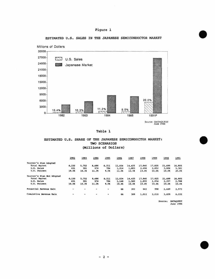
Figure 1
ESTIMATED U.S. SALES IN THE JAPANESE SEMICONDUCTOR MARKET
Millions of Dollars 30000
27000
24000
21000
18000
15000^
12000
9000-1
6000
3000
0
U.S. Sales
Japanese Market
10.4% 10.3% 11.2% 9.5%
20.0%
1982 1983 1984 1985 1991F
Source: DATAQUEST June 1986
Table 1
ESTIMATED U.S. SHARE OP THE JAPANESE SEMICONDUCTOR MARKET: TWO SCENARIOS
(Millions of Dollars)
Yeutter'a Plan Adopted Total Harlcet U.S . Sales U .S. Percent
Yeutter's Plan Not Adopted Total Marlcet U.S. Sales U.S. Percent
Potent ial Itevenue Gain
Cumulative Revenue Gain
1982 1983 1964 1986 1987 1988 1990 1991
4,ISO 431
10.4%
4,150 431
10.4«
5,752 591
10.3%
5,752 591
10.3%
8,S86 974
11.2%
8,6S6 974
11.2%
8,211 784 9.5«
8,211 784 9.5%
11,034 1,214 11.0%
11,034 1,148 10.4%
14,425 1,803 12.5%
14,425 1,500 10.4%
17,840 2,498 14.0%
17,840 1,855 10.4%
17,825 2,852 16.0%
17,825 1,854 10.4%
21,699 3,906 18.0%
21,699 2,257 10.4%
26,805 5,361 20.0%
26,805 2,788 10.4%
66 303 643 998 1 ,649 2,573
66 369 1 ,012 2 ,010 3 ,659 6 ,232
Source: DATAQUEST June 1986
- 2 -
Dataquest TticOt'in&^BradslTcclCutjHHUtroIi
RESEARCH BULLETIN
JSIS Code: Newsletters 1985-1986, JSIA 1986-24
JAPAN'S PUSH INTO OPTOCOMPUTING: SEMICONDUCTOR MAKERS FORM OPTOELECTRONICS CONSORTIUM
SUMMARY
In early May, 13 Japanese semiconductor makers announced the formation of a new joint R&D consortium to develop second-generation optoelectronic ICs (OEICs). Called the Optical Technology R&D Corporation, the new venture plans to invest 3flO billion ($62.5 million) in optoelectronics research during the next 10 years and will involve both government and corporate researchers. The goal of the research consortium is to develop new OEIC process and device technologies for optical communications and future optocomputers.
DATAQUEST believes that this new joint venture highlights the popularity of joint government-industry R&D projects sponsored by private companies. Within the past year, Japanese companies have also formed private R&D consortiums to pursue automotive electronics, diamond substrates, and space-grown materials.
This venture also emphasizes the growing importance of optoelectronic technology. As discussed in our newsletter, "Japanese Technology: The Future Wave" (issued January 7, 1986, see pages 18 and 27), Japanese makers view optoelectronics and optocomputing as the next wave in semiconductor technology during the 1990s. Driven by optical communications, this technology will not only utilize gallium arsenide (GaAs), but also new silicon-GaAs hybrid process technologies.
INCREASING OPTOELECTRONIC IC (OEIC) RESEARCH
Companies involved in the Optical Technology R&D Corporation include Fujikura, Fujitsu, Hitachi, Koga Electric, Matsushita, Mitsubishi, NEC, Nihon Hanshoshi, Oki Electric, Sanyo, Sharp, Sumitomo Electric, and Toshiba. The venture will initially be capitalized at ¥143 million ($894,000). Of this amount, the participating companies will invest ¥43 million ($269,000), or about 30 percent, with the Japanese government financing the remainder. The company, which begins operations in June, plans to invest about ¥100 million ($625,000) in a Basic Technology Research Promotion Center in the Tokyo area.
© 1986 Dataquest Incorporated May—Reproduction Prohibited
The conieni ot ihis repor", represents our mterprelalion and analysis ot mtormation generally available to the public or released by responj ible individuals in the subject companies bui is nol guaranteed as lo accuracy or complfeleness it does not conlain
material oravidea to us m conlioence by our clients Individual complines reponed on and analyzed by DATAQUEST may be clients ol Ihis and/or ottie' DATAQUEST services This mtormalion is nol furnished m connection with a sale or otter to sell securities
or .n connection wIlh the sdicitation of an offer to buy securities This lirm and ils parent and/oi their officers stockholders or members of their families may from bme to lime liave a lorig or short position m the secunties mentioned and may sen or puy sucn securities
Dataquest Incorporated, 1290 Ridder Park Drive, San Jose, CA 95131-2398, (408) 971-9000, Telex 171973
As shown in Table 1, many Japanese companies are focusing on OEICs for optical communications. The first-generation OEICs, which consist of LEDs, light-receiving devices, and transistors, have already been introduced. The new research consortium will initially focus on second-generation OEICs capable of handling 1-gigabit-per-second (Gbps) optical transmission, with the ultimate goal of developing OEICs capable of 10-Gbps speeds.
DATAQUEST notes that OEICs will play a key role in Nippon Telegraph and Telephone's (NTT) Information Network System (INS). In 1984, NTT completed installation of a 1,250-mile, 400-Mbps optical-fiber cable from northern Hokkaido to southern Kagoshima. In 1987 or 1988, NTT plans to install a 1.6-Gbps optical-fiber cable between Tokyo and Osaka. A 12-mile experimental cable is now being tested in Kawasaki. With the merger of communications, computer, and optical-storage technology, we believe that OEICs will become a critical semiconductor technology that U.S. and European companies cannot afford to overlook.
Sheridan Tatsuno
Table 1
FIRST-GENERATION JAPANESE OPTOELECTRONIC ICs (OEICs)
Group
F u j i t s u
H i t a c h i
Kyoto University
Date Device
Q2/85 An experimental OEIC transmission method using an integrated semiconductor laser and four FETs on a GaAs substrate
Ql/86 An 1.6 X 1.0mm OEIC incorporating laser diodes, lightwave paths, and optical switch for optical exchanges and optical computers
Ql/86 An InP/InGaAsP OEIC that combines phototransistors and LEDs for high-speed signal processing and optical telephone exchanges
Matsushita Q4/84 world's first optical integrated device consisting of a semiconductor laser and transistors for optical memories and inverters
MITI Ql/86 A new optical phenomenon for developing optical isolators and OEICs
NEC
Optical Technology Joint R&D Center
Ql/86 An OEIC integrating three lasers, a photodiode, and three transistors that is capable of sending 1.2 Gbps of data through ultrahigh-speed, long-wavelength-band, fiber-optic transmission systems
Q3/85 A new epitaxial crystal growth technique for OEICs that integrates laser diodes with transistors
Tokyo Ql/86 A prototype optical computer system using ten University lenses and OEICs
Tokyo Institute of Technology
Ql/86 An OEIC consisting of laser diodes and optical switching for use in future optocomputers
Source: DATAQUEST May 1986
- 2 -
DataQuest n n ^'KmiiMrivut MMMB rhcniinK'ttnicJsIricctCorpi
JAPANESE RESEARCH
NEWSLETTER
JSIS Codes Newsletters 1985-1986, JSIA 1986-23
THE DOUBLE WHAMHY: YEN APPRECIATION AND U.S. DUMPING MARGINS
SUMMARY
Within the last few months, Japanese semiconductor makers have been hit hard by U.S. dumping margins and the appreciation of the yen. Both factors have pushed up Japanese costs for EPROMs and 64K and 256K DRAMs by 83 to 250 percent since March 1985. To maintain market share, especially in the face of South Korean competition, Japanese companies are adopting several strategies, including:
Raising component and equipment prices to only what the marlcet will bear
Moving manufacturing offshore, especially to southeast Asia and the United States
• Investing in new U.S. wafer fabs
• Diversifying into ASICs, MPUs, linear, and other memory areas
DATAQUEST believes that the current dumping margins only provide a temporary breathing space for U.S. makers. By 1987, we expect top Japanese semiconductor makers to be producing a more diversified product line in the United States. As in the automobile market, the price pressure from Japan and South Korea will be strong. U.S. semiconductor makers must increase their R&D, automate their plants, and build stronger ties with users to maintain market share.
© 1986 Dataquest Incorporated May—Reproduction Prohibited
The content of this report represents our interpretation and analysis of information generally available to the public or released by responsible individuals in the subject companies, but is not guaranteed as to accuracy or completeness It does not contain material provided to us in confidence by our clients Individual companies reported on and analyzed by DATAQUEST, may be clients of this and/or other DATAQUEST services This information is not furnished in connection with a sate or offer lo sell securities or in connection with the solicitation of an offer lo buy securities This firm and lis parent and/or their officers, stixkholders, or members of their families may, from time to lime, have a long or shorl position in the secunties mentioned and may sell or buy such securities
Taiyo Ginza Building / 7-14-16 Ginza, Chuo-ku / Tokyo 104, Japan / (03) 546-3191 / Telex J32768 1290 RIdder Park Drive / San Jose, CA 95131-2398 / (408) 971-9000 / Telex 171973
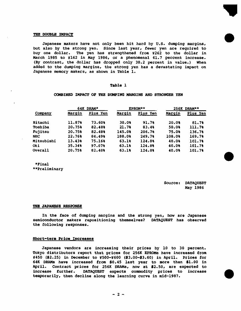
THE DOUBLE IMPACT
Japanese makers have not only been hit hard by U.S. dumping margins/ but also by the strong yen. Since last year, fewer yen are required to buy one dollar. The yen has strengthened from ¥262 to the dollar in March 1985 to 3fl62 in May 1986, or a phenomenal 61.7 percent increase. (By contrast, the dollar has dropped only 38.2 percent in value.) When added to the dumping margins, the strong yen has a devastating impact on Japanese memory makers, as shown in Table 1.
Table 1
COMBINED IMPACT OF THE DUMPING MARGINS AND STRONGER YEN
Company
Hitachi Toshiba Fujitsu NEC Mitsubishi Oki Overall
*Final **Preliminary
64K Margin
11.87% 20.75% 20.75% 22.76% 13.43% 35.34% 20.75%
DRAM* Plus Yen
73.60% 82.48% 82.48% 84.49% 75.16% 97.07% 82.48%
EPI Margin
30.0% 21.7%
145.0% 188.0% 63.1% 63.1% 63.1%
iOM** Plus Yen
91.7% 83.4% 206.7% 249.7% 124.8% 124.8% 124.8%
256K Margin
20.0% 50.0% 75.0%
108.0% 40.0% 40.0% 40.0%
DRAM** Plus Yen
81.7% 111.7% 136.7% 169.7% 101.7% 101.7% 101.7%
Source: DATAQUEST May 1986
THE JAPANESE RESPONSE
In the face of dumping margins and the strong yen, how are Japanese semiconductor makers repositioning themselves? DATAQUEST has observed the following responses.
Short-term Price Increases
Japanese vendors are increasing their prices by 10 to 30 percent. Tokyo distributors report that prices for 256K EPROMs have increased from 3f450 ($2.25) in December to ¥500-Y600 ($3.00-$3.60) in April. Prices for 64K DRAMS have increased from $0.45 last year to more than $1.00 in April. Contract prices for 256K DRAMs, now at $2.50, are expected to increase further. DATAQUEST expects commodity prices to increase temporarily, then decline along the learning curve in mid-1987.
- 2 -
Assembly and Testing in Southeast Asia
To get around the dumping margins, Japanese vendors are shipping DRAMs and EPROMs through Singapore, Hong Kong, and Malaysia, often with the tacit support of major U.S. users. Japanese vendors are also expanding ttieir assembly and testing operations in Southeast Asia to reduce manufacturing costs, since the currencies in these countries are closely tied to the U.S. dollar. Hitachi, for example, recently doubled 256K DRAM production in Malaysia.
More U.S. Production and Investments
DATAQUEST expects Japanese makers to invest in wafer fabs in the United States during 1986 to counter the dumping margins and strong yen. NEC, which has a state-of-the-art fab in Roseville, California, plans to ramp up production of memories, ASICs, and other products. Hitachi is accelerating construction of its Irving, Texas, fab, while Mitsubishi is planning a fab in the Research Triangle in North Carolina. Other Japanese makers have a strong incentive to follow suit, since the yen buys 61.7 percent more U.S. plant and equipment than last year.
Diversification to Higher Value-added Products
Until these new fabs come on-line, Japanese vendors are diversifying their product portfolios. In particular, gate arrays, telecom ICs, microprocessors, and linear ICs are attracting attention. As a result, DATAQUEST believes Japanese product diversification will intensify price pressures on U.S. makers in high-value-added and niche markets. We expect ASICs to become the next major battleground, especially high-volume CMOS gate arrays.
It is possible that Japanese vendors may end up stronger, not weaker, as a result of the dumping margins and yen appreciation. In particular, Japanese companies have a strong incentive to invest in the United States because of the strong yen, while U.S. companies may cut back their Japanese investment plans. The long-term implications of these short-term responses will be serious for both industries.
Sheridan Tatsuno
- 3 -
DataQuesl 3 tompanv f il I hi' Chin 1^ fir ; I I1M tn;I L < H pur j lu M >
JAPANESE RESEARCH
NEWSLETTER
JSIS Code: Newsletters 1985-1986, JSIA 1986-21
DATAQUEST'S SECOND ANNUAL JAPANESE SEMICONDUCTOR INDUSTRY CONFERENCE: FUTURE VLSI AND APPLICATIONS
SUMMARY
DATAQUEST's Second Annual Japanese Semiconductor Industry Conference was held April 13-15, 1986, in Hakone, Japan. With Mount Fuji dominating the spring skyline, 243 attendees from Japan, Taiwan, Korea, Hong Kong, China, the United States, France, Italy, the United Kingdom, and Germany gathered to discuss the status and future of the semiconductor industry.
At this conference it was generally agreed that the future lies from the Pacific Basin westward.
Although the conference was held in the wake of preliminary U.S. dumping rulings against Japanese manufacturers and stalled U.S.-Japan semiconductor negotiations, trade was not a major topic of speeches or conversation.
Highlights of the conference included:
• A speech by Wang Zhenghua, a Chief Engineer of the China National Electronic Devices Corporation (Due to Japan-China friction, Mr. Wang and his colleague. He Mingzhang, received their Japanese visas only one day before their flight to Japan)
• A speech by Dr. Yasusada Kitahara, Senior Executive Vice President of NTT and a highly venerated figure in the Japanese semiconductor industry
Keynote Speakers
The conference featured two keynote speakers: Gary L. Tooker, Executive Vice President and General Manager of Motorola, Incorporated; and Hiroshi Asano, Executive Vice President of Hitachi, Limited.
© 1986 Dataquest Incorporated May—Reproduction Prohibited
The content of this report represents our interpretation and analysis of information generally available lo the public or released by resfxinsible individuals in the subject companies, but is not guaranteed as to accuracy or completeness It does not contain material provided to us in confidence by our clients Individual companies reported on and analyzed by DATAOUEST, may be clients of this and/or other (DATAQUEST services This information is not furnished in connection with a sate or offer to sell securities or in connection with the soliatalion ot an offer to buy securities This firm and its parent and/or their officers, stockholders, or memtiers of their families may, from lime to time, have a long or short position in the securities mentioned and may sell or buy such securities
Taiyo Ginza Building / 7-14-16 Ginza, Chuo-ku / Tokyo 104, Japan / (03) 546-3191 / Telex J32768 1290 Ridder Park Drive / San Jose, CA 95131-2398 / (408) 971-9000 / Telex 171973
Mr. Tooker targeted his speech directly at the U.S.-Japan trade friction, with the theme "Technology and Trade," or "T&T." He called for the forging of a "win-win" strategy in resolving the technology and trade issues between the United States and Japan, pointing out the strategic importance of the U.S. semiconductor industry to the military defense of the United States, Japan, and the rest of the free world. He called for the Japanese to open their semiconductor market to U.S. suppliers, who have proven their ability to deliver high-quality product on time.
Mr. Asano directed his speech at the growth of the Information Age and the tools that support this growth. Comparing the long-term growth rates of the three major segments of Japan's electronics industry, electronic components and industrial (including information processing) production far outpaced consumer electronics production. Mr. Asano believes that software is the wave of the future, and is a challenge for Japanese industry. Contrary to hardware, which requires mass production and mass sales, software requires a broad product lineup, small-quantity production, and value-added resales. He predicts that the largest software market worldwide will be for small computer terminals and office automation, where he believes demand will outstrip supply.
SPEECHES
Conference attendees listened to two jam-packed days of speeches, simultaneously translated from Japanese to English and vice-versa (or from Chinese to Japanese to English, in the case of Mr. Wang), on a variety of topics germane to today's industry.
Major categories of speeches were as follows:
DATAQUEST's forecasts and analyses
Specific VLSI applications
Chips for the future
Strategic alliances
Status of Other Far East semiconductor industries
DATAQUEST's Forecasts and Analyses
Osamu Ohtake, Associate Director of DATAQUEST's Japanese Semiconductor Industry Service, opened the conference with an overview of the increasingly important position of Japan and Japanese companies in the worldwide semiconductor industry. Of particular note are:
• NEC's ascent to the number one position among suppliers worldwide
• The fact that the top ten suppliers in the world all had decreased revenues in 1985, the worst semiconductor recession ever
- 2 -
• The continuing loss of market share by U.S. and European manufacturers to Japanese and Asian manufacturers
• The continuing trend toward U.S./European partnerships with Japanese companies, particularly in CMOS
Nagayoshi Nakano, DATAQUEST Research Analyst, presented an overview of semiconductor application trends in Japan. He expects semiconductor consumption to continue to outpace the end equipment market, due to increasing semiconductor pervasiveness. The industrial segment of the market is growing more rapidly than the consumer segment. The fastest-growing end markets are digital audio disk players, word processors, and facsimiles.
Comparing the semiconductor markets of Japan, the United States, and Europe, Mr. Nakano portrayed the Japanese market as the overall leader, due to the differing market structures:
• The U.S. market is oriented toward data processing and industrial uses, resulting in high growth during prosperity and huge decline during recessions—a highly volatile market.
• The European market is well balanced by end use, resulting in years of low growth and small declines—a highly stable market.
• The Japanese market is oriented toward consumer and data processing usage, resulting in high growth during prosperous years and only small declines in recession years such as 1985.
Lane Mason, DATAQUEST Senior Industry Analyst, spoke on the future outlook for MOS memory. He painted a bleak picture, focusing on the horrendous losses suffered by all MOS memory suppliers in 1985. He presented a number of issues facing MOS memory manufacturers, including:
• What are our motives (i.e., technology development, visibility)?
• How can we form a strategy to counter the seemingly inevitable cyclical nature of this business?
• In 1981, the worldwide MOS memory market fell 17 percent; in 1985, it fell 39 percent. DATAQUEST forecasts that the next downturn will be in 1989, when MOS memory will decline at least 11 percent.
VLSI Design, Fabrication, and Testing
Al Stein, Chairman and CEO of VLSI Technology, Inc., spoke on "Design Solutions with ASICs." Focusing on the user-specific portion of the ASIC market (chips designed as proprietary products for specific users), he spoke on the many benefits of using ASIC technology in systems. ASIC technology has become preeminent because of these benefits—such as higher system performance, improved engineering productivity, and reduced
- 3 -
system size and cost—combined with new tools to make ASIC production more efficient—such as simpler workstation access, integrated design environment, reduced cycle time, and greater use of automation.
Mr. Stein analyzed the differing design needs of various customers, and classified three major needs:
• High performance: full-custom design, fairly low gate count, driven by a need for very high speed
• High integration: very high gate count, standard and compiled cell design, driven by desire to have a system on a chip
• Simple integration: very low gate count, standard cell design, used to replace TTL, driven by cost reduction
"The Impact of VLSI on Automatic Testing" was the topic presented by Alex d'Arbeloff, President and CEO of Teradyne Incorporated. Mr. d'Arbeloff pointed out the mounting costs of testing as circuits become increasingly complex. For transistors, testing represents only 5 percent of total production cost; for LSI the figure is 20 percent; and for VLSI ICs, 40 percent of product cost is testing. Obviously, cost-cutting strategies for VLSI testing are a necessity. Mr. d'Arbeloff's suggestions on ways to cut test costs include:
Designing for testability
Using common simulation software
Using self-test techniques
Using parallel/multiplex testing
Using nonstop testing
Tames C. Morgan, President and CEO of Applied Materials Incorporated, spoke on "Supporting the Transition to VLSI Fabrication." Mr. Morgan discussed the necessity of orienting semiconductor processing equipment to the needs of sub-1-micron, isolation trenches, and multilevel polysilicon and metal processing. Also, equipment must become more productive in order to reverse the trend toward increasing capital intensity. Mr. Morgan stressed the need for extendable equipment technology, process flexibility, and preventive maintenance as ways of achieving effective, cost-efficient production.
James Springgate, President of Monsanto Electronic Materials Company, addressed the topic, "Silicon and Semiconductors—Partners in the '80s." Mr. Springgate expects significant change in the next five years as silicon suppliers adapt to t±e needs of VSLI and its manufacturers. Among the significant trends he foresees are 200 and 250mm diameter wafers, wafers tailored to specific IC applications, wafers designed specifically for emerging VLSI applications (this is currently a state-of-the-art research area), and advanced epitaxial wafers.
- 4 -
Specific VLSI Applications
Automotive semiconductor applications were covered in two speeches, one by Dr. Charles Tracy, Chief Engineer at Delco Electronics Corporation; the other by Masao Murayama, Executive Managing Director of Nippondenso Company, Limited.
In both Japan and the United States, nonradio ICs made their first appearance in cars in 1968. In both countries, engine control ICs were introduced around 1980 to comply with U.S. government emission and fuel economy requirements. Functional content has dramatically increased over the intervening years, while die size has seen a comparable decrease.
Both speakers described the "chip of the future" for advanced electronic engine control. This chip would be a single-chip MCU with RAM, ROM, timer, and A-D converter. The chip would also be available in EPROM or E^pROM versions in order to provide more flexibility and meet customers' demands.
Fumio Kohno, Senior General Manager of Sony Corporation's Semiconductor Group, spoke on "Future VLSI and Consumer Electronics." Mr. Kohno spoke of the "Needs and Seeds" relationship between consumer electronics and semiconductor technology. Semiconductor technology has advanced because of the Needs of consumer electronics, while the Seeds (semiconductor technology innovations) have in turn made it possible to make better, more advanced consumer electronic products. He expects increased use of digital ICs in consumer products to significantly enhance performance.
Mr. Kohno cited several examples of the Needs/Seeds relationship:
• 8mm VTRs were made possible by high-density hybrid ICs and PCM audio signal processing LSIs.
* Digital audio tapes were made possible by low-power linear ICs, A-D/D-A converters for digital audio, and digital signal processing LSIs.
In the past, consumer electronics needs pushed IC technology, but in the future (in Mr. Kohno's opinion), IC technology seeds will drive consumer electronics technology.
Noriaki Shimura, Managing Director of Casio Computer Company, Limited, spoke on "Application Strategies for Success." Casio is a ¥200 billion ($1.1 billion) company that consumes more than 10 million integrated circuits per month, approximately 90 percent of which are custom LSI ICs. Casio designs one-third of the custom chips it uses; however, all production is done by one or two semiconductor vendors. The relationship between these suppliers and Casio engineers is viewed by Mr. Shimura as being of strategic importance to the successful evolution of Casio products.
- 5 -
Dr. Yasusada Kitahara, Senior Executive Vice President of Nippon Telegraph and Telephone Corporation, is a highly revered figure in the Japanese semiconductor industry. Dr. Kitahara's topic was "VLSI Applications, INS, and the Future." Dr. Kitahara spoke of the importance of VLSI and VLSI technology in making Japan's INS (Information Network System) a reality.
Chips for the Future
This subject was taken up by four speakers:
• Dr. Tsugio Makimoto, General Manager of Hitachi Limited's Musashi Works
41 Donald W. Brooks, President and CEO of Fairchild Semiconductor Corporation
• Minoru Yoshida, President of Tokyo Electron Limited
• Kimio Sato, Senior Managing Director of Mitsubishi Electric Corporation
Dr. Makimoto of Hitachi coined a new term—UFIC—for User-Friendly Integrated Circuit. UFlCs are defined as devices that facilitate movement from a user's concept of a system to implementation of the actual system in the shortest time possible. Hitachi's answer to this is its ZTAT (zero turnaround time) microcontroller with built-in EPROM.
Fairchild's Don Brooks focused on the trend toward CMOS, BiMOS, and GaAs ICs in order to achieve the performance standards required for supercomputers, minisupercomputers, and advanced workstations. He also spoke Of the overriding importance of the customer-vendor relationship in producing chips to meet the customers' needs.
Minoru Yoshida of Tokyo Electron Limited (TEL) spoke on "Japanese Initiative and Cooperation in High-Tech Industry." His focus was on cooperation, and he outlined TEL's partnerships with the U.S. equipment makers Thermco, Genrad, Varian, and Lam Research. He pointed out the complementary nature of the Japanese strengths of employee loyalty, good production engineers, and lifetime employment, with the U.S. strengths of conceptual ability in system design and the U.S. educational system.
Kimio Sato of Mitsubishi gave a "Perspective for the 1990s." He believes that in 1990 only 60 percent of semiconductor demand will be related to equipment that exists today. He expects discretes to dramatically decrease as a percentage of total semiconductor consumption. MOS logic, micro devices, and memory will supply many of the new markets: electronic files, electronic "secretaries" (i.e., the ability to schedule appointments remotely via a wristwatch computer), telecomputer conferences, video conferences, telecommuting, artificial intelligence, automatic translation, automatic readers, IC cards, and robots.
- 6 -
strategic Alliances
The topic Of strategic alliances (joint ventures, partnerships, licensing, technology exchange, mergers and acquisitions, and so forth) was addressed by Keiske Yawata, President and CEO of LSI Logic K.K., and James Riley, Senior Vice President of DATAQUEST.
Mr. Yawata focused on alliances in the ASIC area. Japanese "user friendliness" can be used to the advantage of U.S. companies for high-density packaging using surface-mount technology and leadless chip carriers. An ideal corporate alliance is a perfectly complementary relationship without conflict of interest.
Mr. Riley pointed out the necessity of forming international partnerships in order to maintain or gain market share in an increasingly global market. Strategic alliances in the global marketplace can give a company informed market presence and cultural synergy, as well as complementary assets.
Status of Other Far East Semiconductor Industries
Leaders from the semiconductor industries of Taiwan, Hong Kong, and China gave reports on the status and future outlook of their areas. These three speakers were:
•: Dr. Chintay Shih, Vice President and ERSO General Manager, ITRI
• C. D. Tam, Vice President and General Manager (Asia), Motorola, Incorporated
• Wang Zhenghua, Chief Engineer of IC Design Center, China National Electronic Devices Corporation
Dr. Shih of ITRI stated that Taiwan currently has 2 silicon wafer manufacturers, 3 fabrication facilities, 1 maskmaking company, 11 design centers, and 26 assembly plants (many are foreign owned). The Taiwanese government is sponsoring a plan to build a large, VLSI wafer fabrication facility to do foundry work. The plant will have 10,000 6-inch wafer starts per month capacity in 1987, expanding to 40,000 starts per month by 1990. Dr. Shih also discussed Taiwan's "Multi Project Chip," which is a national training effort, at the university level, that allows students to design and process ICs. This results in graduates who are ready to contribute to Taiwan's fast-growing IC industry.
Motorola's C. D. Tam spoke on "The Asia/Pacific Electronics Industry—An Industry in Transition." He focused on the "Four Tigers of the Orient"—Hong Kong, Korea, Singapore, and Taiwan. These countries showed higher growth in electronic production from 1977 to 1983 than Japan, the United States, and Europe. While consumer electronics still represents the largest single end market for semiconductors in the Four Tigers, it has steadily decreased, from 89 percent to 44 percent. Growth of personal computers, PCs, and other computers has been steady and dramatic since 1980.
- 7 -
The Four Tigers are now poised to enter the high-level system market—large PABXs, digital televisions, mini and mainframe computers, robotics, and factory automation systems. Design of these systems will be facilitated by two semiconductor technologies:
• New LSI/VLSI chips, such as DSP and 32-bit microprocessors
• ASICs and user-friendly CAD tools
Wang Zhenghua from China's National Electronic Devices Corporation, gave a comprehensive overview of the People's Republic of China's semiconductor industry. China has 450 semiconductor plants located in 28 provinces, mostly near large cities. Two hundred thousand people work in the semiconductor industry. Ten billion semiconductor devices, including 50 million ICs, were produced in 1985.
IC production in China began in 1966, a major quality improvement program was instituted in 1970, and by 1978, quality had reached international standards. China has five bipolar IC techologies—TTL, STTL, LSTTL, HTL, and ECL. There is production of PMOS logic, CMOS, and NMOS. Current capabilities are for 5 to 7u processing, and work is progressing on 3u processing. Research has been completed on 16K DRAMs and SRAMs, and 4- and 8-bit microprocessors are being produced. Linear IC production includes op amps, voltage regulators, and consumer chips for television, audio, and watch applications.
DATAQUEST CONFERENCE NOTEBOOK
All conference attendees received a comprehensive conference notebook with a list of attendees and copies of the conference speeches. This notebook will be mailed this month to all JSIS clients who did not attend the conference. If you wish to read these proceedings, please contact your JSIS notebook holder.
Patricia S. Cox
- 8 -
Dataquest ftic OiAn&'tinidslKcl Corporalioti
RESEARCH BULLETIN
JSIS Code: Newsletters 1985-1986, JSIA 1986-22
MITI OFFERS PROPOSAL TO AVOID DUMPING PENALTIES
SUMMARY
Japan's Ministry of International Trade and Industry (MITI) has proposed a semiconductor monitoring system in an effort to avoid the implementation of dumping penalties on Japanese DRAMs and EPROMs. The MITI proposal was published in a prominent Japanese industrial journal, Nihon Keizai, as a "trial balloon" to elicit an official U.S. response. MITI has used this procedure in the past to test public and industry reaction to policies that were later made official. The new proposal includes the following:
• A demand-supply guidepost system to curb overproduction and stabilize prices
• A lowest-export-price system (price floor) to prevent below-cost sales (dumping)
• A uniform minimum price system to prevent circuitous exports to the United States or elsewhere through third countries (Europe and Asia)
Under the new system, similar to MITI's control of Japanese iron and steel production, a select committee will announce a quarterly semiconductor demand-supply outlook. If production plans exceed consumption forecasts, MITI will request Japanese vendors to reduce their production plans. Both the Japanese and U.S. goverrunents will negotiate fully loaded production costs to determine price curves.
DATAQUEST ANALYSIS
The main reason for MITI's proposal can be seen in Table 1. In addition to the dumping penalties, the current dollar/yen exchange rate compounds export difficulties and will continue to be a problem regardless of any decision about dumping penalties. For this reason, MITI believes that dumping penalties are adding insult to injury.
1986 Dataquest*Incorporated May—Reproduction Prohibited
The conlenl ol this repor". rep'ssen's ow interDfelalion and anaiy!?<s o( information genefally available io [he pubic or released by responsible individuals in the subject companies but is not guaranteed as lo accuracy or completeness It does not contam
maieriai provioed to us m coniidence by OLir clients Individual companies reported on and analyzed by DATAQUEST may be chenls o' this and/or other DATAQUEST services This mlormation is not 'urnished in connection with a saie or oHpr lo seli securities
or .n connection with the solicitation ol an otier to buy aecunties Tins !irm and ils parent ana/or their officers stockholders or niembers ol Iher lamiiies m^y trom time to lime have a long or shoil position m the securities mentioned and may seli or buy such securities
Dataquest Incorporated, 1290 Ridder Park Dnve, San Jose, CA 95131-2398, (408) 971-9000, Telex 171973
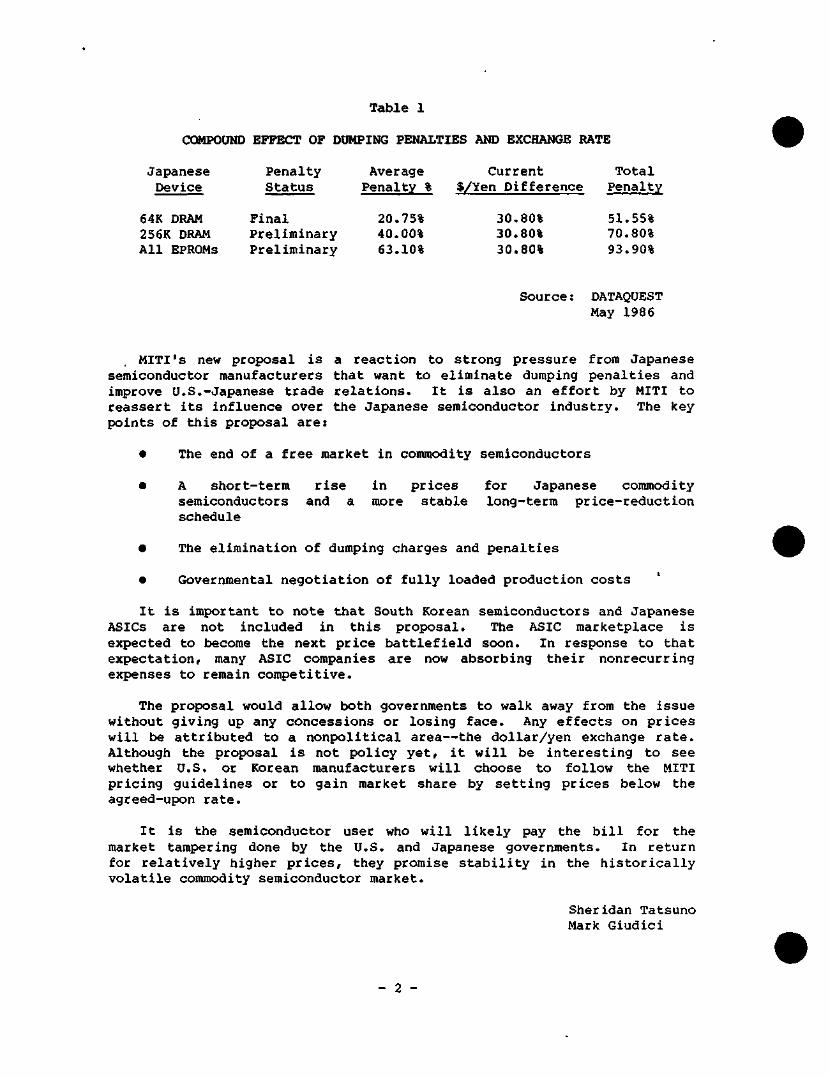
Table 1
COMPOUND EFFECT OF DUMPING PENALTIES AND EXCHANGE RATE
Japanese Penalty Average Current Total Device Status Penalty % $/Yen Difference Penalty
64K DRAM 256K DRAM All EPROMs
Final Preliminary Preliminary
20.75% 40.00% 63.10%
30.80% 30.80% 30.80%
Source:
51.55% 70.80% 93.90%
DATAQUEST May 1986
MITI's new proposal is a reaction to strong pressure from Japanese semiconductor manufacturers that want to eliminate dumping penalties and improve U.S.-Japanese trade relations. It is also an effort by MITI to reassert its influence over the Japanese semiconductor industry. The key points of this proposal are:
• The end of a free market in commodity semiconductors
• A short-term rise in prices for Japanese commodity semiconductors and a more stable long-term price-reduction schedule
• The elimination of dumping charges and penalties
• Governmental negotiation of fully loaded production costs
It is important to note that South Korean semiconductors and Japanese ASICs are not included in this proposal. The ASIC marketplace is expected to become the next price battlefield soon. In response to that expectation, many ASIC companies are now absorbing their nonrecurring expenses to remain competitive.
The proposal would allow both governments to walk away from the issue without giving up any concessions or losing face. Any effects on prices will be attributed to a nonpolitical area—the dollar/yen exchange rate. Although the proposal is not policy yet, it will be interesting to see whether U.S. or Korean manufacturers will choose to follow the MITI pricing guidelines or to gain market share by setting prices below the agreed-upon rate.
It is the semiconductor user who will likely pay the bill for the market tampering done by the U.S. and Japanese governments. In return for relatively higher prices, they promise stability in the historically volatile commodity semiconductor market.
Sheridan Tatsuno Mark Giudici
- 2 -
DataQuest aiompanvol Tlw; Dun K BiatistmelCorpgralion
JAPANESE RESEARCH
NEWSLETTER
JSIS Code: Newsletters 1985-1986, EIEJ 1986-20
KOREAN TAXATION
INTRODUCTION
DATAQUEST recently completed and published its first in-depth analysis of the Korean semiconductor industry. The report showed the total capital investment of the native Korean manufacturers for 1984 and 1985 to be $1,114 billion. This investment was almost four times their combined revenues.
In our Korean report, we also referred to the considerable tax incentives that befall the native companies that are investing in electronics and semiconductors. For example, these companies receive an additional depreciation of 100 percent of normal depreciation on capital goods. This accelerated depreciation is, of course, meant to enable these corporations to enter the world electronics market in the most expedient manner.
We believe that companies that are looking at Korea as a future manufacturing site or at the native manufacturers as competitors should be familiar with the Korean tax legislation and administration. To this end, we have prepared the following review and summary to supplement the initial Korean report.
KOREAN TAXATION
Tax Legislation and Administration
Under the Korean Constitution, tax legislation is enacted by the National Assembly. Proposed tax legislation is drafted by the related ministries (e.g., national taxes by the Ministry of Home Affairs) and submitted to the National Assembly through a resolution by the State Council. Such proposals may also be submitted by members of the National Assembly. The new tax laws are transmitted to the Administration for promulgation by the president. The president is empowered to issue
© 1986 Dataquest Incorporated April 18 ed.-Reproducton Prohibited
The content of this report represents our interpretation and analysis of information generally available to the public or released by responsible individuals in the subject companies, but is not guaranteed as to accuracy or completeness It does not contain material provided to us in confidence by our clients Individual companies reported on and analyzed by DATAQUEST may be clients of this and/or other DATAQUEST services This information is not furnished in connection with a sale or offer to sell securities or in connection with the solicitation of an offer to buy securities. This firm and its parent and/or their officers, stockholders, or memtiers of their families may, from time to time, have a long or short position in the securities mentioned and may sell or buy such securities.
Taiyo Ginza Building / 7-14-16 Ginza, Chuo-ku / Tokyo 104, Japan / (03) 546-3191 / Telex J32768 1290 Ridder Park Drive / San Jose, CA 95131-2398 / (408) 971-9000 / Telex 171973
presidential decrees concerning matters entrusted within the jurisdiction of the legislative body. The law takes effect 20 days after promulgation, unless otherwise provided. Generally, changes in Korean tax laws become effective on the first day of January of the following year.
The administration of national taxes is under the jurisdiction of the Ministry of Finance, which may issue ordinances for the implementation of the national tax laws and related presidential decrees after being empowered by a presidential decree. However, the authority for issuing the ordinances is delegated to the Office of National Tax Administration. These ordinances frequently cover matters that are too technical or complex to be set forth in detail in the statutes. Such ordinances have the force of law and often contain detailed instructions for the taxpayer to follow in computing and paying his tax.
, Within the Ministry, the Office of National Tax Administration (ONTA) is responsible for the actual administration of the tax laws.
Features of the Korean Tax System
The Korean tax system consists of internal taxes, customs duties, and defense tax. The internal taxes encompass, among others, an income tax, a value-added tax, and a special excise tax.
The income tax laws generally distinguish between taxpayers that are legal entities and individuals. Individual income is classified into the categories of global income, timber income, retirement income, and capital gains. Each income category is subject to a separate, progressive income tax, except for capital gains, which are taxed at a flat rate. The tax rates apply to both residents and nonresidents. Corporations are taxed on their income at progressive rates. Tax credits are allowed to corporations for income taxes paid abroad under certain conditions.
Dividends received are taxable. Dividends paid to nonresident foreign shareholders are subject to withholding taxes at source.
The Defense Tax Law was enacted in 1975 to fund government activities related to national defense. The defense tax is a surtax on internal taxes (other than value-added tax) and is also levied on importations that are subject to custom duties. The Defense Tax Law provides an extensive system of withholding tax at source, including withholding from wages, commissions, professional fees, dividends, and interest.
Taxation of Foreign Corporations
A foreign corporation is liable to a corporation tax only on income derived from sources within Korea. However, no corporation tax is levied on the liquidation income of a foreign corporation. Corporation tax on income from domestic sources of a foreign corporation is assessed and collected in the same manner as that applied to a domestic corporation.
- 2 -
with respect to the income from domestic sources of a foreign corporation that has no domestic place of business, the full amount of corporation tax withheld thereon at source is payable to the Korean government.
The provisions of the tax laws with respect to calculation of taxable income and tax amount, assessment, collection, tax withholding, and ceportings for domestic corporations are applicable to foreign corporations having a domestic place of business. However, there are special provisions for foreign corporations which are preferentially applied to.
Tax Incentives
General Principle
Foreign-invested enterprises are domestic enterprises as established by domestic law. Therefore, taxes for foreign-invested enterprises as well as domestic enterprises are not levied or are reduced in accordance with the Income Tax Law, Corporation Tax Law, and Tax Exemption and Reduction Control Law (TERCL), etc. However, in order to encourage foreign investment in Korea, the Foreign Capital Inducement Law (FCIL) provides a broad range of exceptional tax benefits for foreign-invested companies and foreign investors.
Foreign investors or foreign-invested companies that cannot receive tax benefits according to FCIL have tax benefits according to TERCL along with domestic investors. Also, foreign enterprises can receive not only tax exemptions of income tax and corporation tax from FCIL, but also tax exemptions from TERCL.
However, to avoid double exemption from FCIL and TERCL on stocks or shares owned by foreign investors, tax credit for investment is exempt in proportion to the ratio of the stock or shares owned by domestic investors.
Tax Incentives under the Tax Exemption and Reduction Control Law (TERCL)
• Tax incentives on key industries
- A resident individual or a domestic corporation that operates in key industries, such as petrochemical, shipbuilding, machinery, electronics, aerospace, steel manufacturing, and other industries enumerated by the law as well as certain mining industries and defense industries, is entitled to additional depreciation of 100 percent of normal depreciation.
- In the case of the machinery and electronics industries, an investment tax credit on the cost of machinery and equipment (3 percent if imported; 5 percent if manufactured locally) can be taken instead of the special depreciation mentioned above.
- 3 -
Tax incentives on small and medium enterprises
- The additional depreciation, generally 50 percent of normal depreciation, is allowed for a small or medium-size company engaged in manufacturing or mining. Also, a small or medium-size company engaged in manufacturing, mining, construction, transportation, or the operation of a fishery is entitled to a deductible investment reserve of 15 percent of the total machinery and equipment used in the business as of its financial year end.
Tax incentives on development of technology and manpower
- Reserves for technological development being counted in losses in calculating an income amount for the business year
- Tax credit for development of technology and manpower
- Tax incentives for starting a business using new technology
,. An amount equivalent to 6 percent (10 percent in the case of Investment using domestically produced materials) of the amount invested in the business assets is deducted from the income tax or the corporation tax for the business year in which the date of completing said investment falls.
• An amount equivalent to 50 percent of the ordinary depreciation amount is counted in losses in calculating an income amount for the business year, in addition to the ordinary depreciation.
Tax exemption for income for the transfer or lease of a patent
- Deduction for a technology service business
Exemption of a foreign engineer or technician from income taxes on his salary or wages received from a domestic employer for the first five years
Tax incentives for a business earning foreign currency
- Reserves falling under the following categories are counted in losses
» Reserves for export loss
i Reserves for overseas market development
- 4 -
Reserves for price fluctuation of export goods
Special depreciation
Supply of the goods for exportation and services rendered outside Korea is zero-rated in value-added tax
Tax incentives for defense industries
S£>ecial depreciation
Exemption of special excise tax
Tax incentives for the encouragement of investment
Tax credit for investment in special equipment—Where a resident or a domestic corporation starting a business using new technology invests in one of the following items, tax incentives described in "Tax incentives for starting a business using new technology" under previous section "Tax incentives on development of technology and manpower" apply:
Facilities for increasing productivity
Energy-saving facilities
Antipollution facilities
Facilities for prevention of industrial hazards
Mine safety facilities, etc.
- Temporary tax credit for investment by the government to regulate the business cycle
Tax credit for investment in housing for homeless employees
Tax incentives for an international monetary organization
Other tax incentives
Capital gains
Overseas business and overseas investment
- Resources development business
Exemption of special excise tax
For materials and goods for equipment required in the construction or repairing of tourist hotels
On goods to be used for Seoul Olympic and Seoul Asia Sports meetings, etc.
- 5 -
I
Tax Privileges under Foreign Capital Inducement Law (FCIL)
• General principle
- Any foreign-invested project is deemed to contribute greatly to the development of the national economy, and when a request is made to receive tax benefits, adjusted tax benefits may be given if the project meets certain criteria. In such cases, the period of exemption is five years. The government permits a foreign-invested enterprise or foreign investor to choose the period for exemption of corporate and dividend income tax from any consecutive five-year period within ten years from registration of the enterprise in order to give the enterprise the maximum benefit from exemption.
- Instead of a direct tax exemption, foreign-invested enterprises may choose a special depreciation, which might be more favorable for capital-intensive industries.
Foreign-invested projects that are deemed to contribute greatly to the development of the national economy are categorized as follows:
• A project that makes a significant contribution to the improvement of the international balance of payments
:, A project that is accompanied by advanced technology or large amounts of capital
. A project in which a non-resident Korean national invests in accordance with the law concerning the registration of non-resident Korean nationals
. A project that is located in a free export zone in accordance with the Free Export Zone Establishment Law
. Any other project designated by presidential decree as a project for which tax reduction or exemption is essential in order to induce foreign investiment
(tf Tax exemption and special depreciation
- The method for tax exemption or special depreciation is as follows:
. Income tax or corporation tax on a foreign-invested enterprise is exempt in proportion to the ratio of the stock or shares owned by foreign investors to the stock or shares of the enterprise concerned.
- 6 -
.; An amount equal to 100 percent of the ceiling of allowable depreciation calculated as determined by income tax law, or corporation tax law, multiplied by the foreign investment ratio, is incorporated into necessary expense or expense as special depreciation for calculating the taxable income for each tax year up to the amount invested by a foreign investor.
* Income tax or corporation tax on dividends accruing from the stock or shares acquired by a foreign investor is exempt up to the income accruing for five years after the tax year commencing following the registration of the foreign-invested enterprise.
* Acquisition tax and property tax on the properties acquired and held by a foreign-invested enterprise is exempt for five years from the date of registration in proportion to the foreign investment ratio of the enterprise concerned only when the properties were acquired and held after the registration of the enterprise concerned. If, however, the foreign-invested enterprise has any property before the registration for the original purpose of the project concerned, acquisition tax and property tax shall be exempt for five years from the date of acquisition of the properties in proportion to the foreign investment ratio of the enterprise concerned.
i\ Special depreciation expense may be incorporated into necessary expense or expense from the tax year commencing first following the registration of the foreign-invested enterprise.
Exemption and reduction of customs duties, etc.
- Customs duties, special excise tax, and value-added tax are exempt with regard to the import of the following capital goods:
* Capital goods to be induced by a foreign investor as a subject matter of investment
Capital goods induced by an enterprise in which a foreign investment invests by means of dividends of a foreign-invested enterprise or by means of payment invested by a foreign investor
Tax exemption or reduction on royalties
- Income tax or corporation tax is exempt for five years from the date of acceptance of a report of the contract concerned with the royalties to be acquired by the technology licensor in accordance with the contents of a technology inducement contract.
- 7 -
f 4
Exemption of income tax on wage and salary income
- Income tax on wage, salary, and bonus of a foreign staff working in Korea under a joint venture agreement is fully exempt for five years from the registration date.
Exemption of special excise tax on automobiles
Special excise tax is exempt on Korean-made automobiles (up to three units) purchased initially by any foreign-invested enterprise prescribed in FCIL.
Exemption of defense tax
Persons who are relieved from taxes by FCIL or various treaties are not liable for a defense tax on those segments of tax relief.
Non-taxable capital gains
Capital gains from investment of land or building, subject to the presidential decree, for the establishment of a foreign-invested enterprise under FCIL
Gene Norrett Dr. Mike Bae
- 8 -
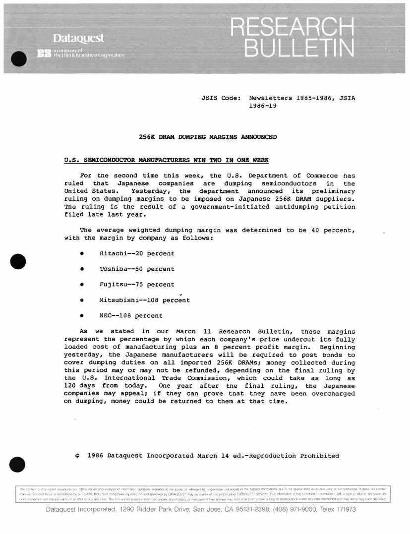
DatnQuest • ;i<iiiiip;iii^ (il
llH't>iiiiJCtti:iilsti(>'U»[j«ir:iin>ri
ESEARGH BULLETIN
JSIS Code: Newsletters 1985-1986, JSIA 1986-19
256K DRAM DUMPING MARGINS ANNOUNCED
U.S. SEMICONDUCTOR MANaFACTURERS WIN TWO IN ONE WEEK
For the second time this week, the U.S. Department of Commerce has ruled that Japanese companies are dumping semiconductors in the United States. Yesterday, the department announced its preliminary ruling on dumping margins to be imposed on Japanese 256K DRAM suppliers. The ruling is the result of a government-initiated antidumping petition filed late last year.
The average weighted dumping margin was determined to be 40 percent, with the margin by company as follows:
Hitachi—20 percent
Toshiba—50 percent
Fujitsu—75 percent
Mitsubishi—108 percent
NEC—108 percent
As we stated in our March 11 Research Bulletin, these margins represent the percentage by which each company's price undercut its fully loaded cost of manufacturing plus an 8 percent profit margin. Beginning yesterday, the Japanese manufacturers will be required to post bonds to cover dumping duties on all imported 256K DRAMs; money collected during this period may or may not be refunded, depending on the final ruling by the U.S. International Trade Commission, which could taKe as long as 120 days from today. One year after the final ruling, the Japanese companies may appeal; if they can prove tnat they have been overcharged on dumping, money could be returned to them at that time.
© 1986 Dataquest Incorporated March 14 ed.-Reproduction Prohibited
The conlenl of Itiis tepon represtinls ouI interpreialion and analysis of Inlormation generally available 10 Ihe pubic or released by responstbie individuals m tbe subject companies bul is not guaranteed as lO accuracy or completeness li does nol coniain
matertal provided to us in conlidence by our clients Individual companies reporled on and analyzed by CATAQUEST may be clients ol Ihis and/or ottier DATAQUEST services This inlormation is nol lurmshed m connection with a sale or offer to sell securities
or in connection wuh the sciicilation ot an offer to buy securities This firm and Its pareni and/or Iheir officers stockholders or members of their tamdies may from time to time, have a long or short position in Ihe securnes mentioned and may sell or buy such securities
Dataquest Incorporated, 1290 Ridder Park Drive, San Jose, CA 95131-2398, (408) 971-9000, Telex 171973
DATAQUEST ANALYSIS
We believe that it is very significant that the U.S. government is now establishing a pattern of supporting the domestic semiconductor industry through the EPROM and 256K DRAM antidumping rulings this weeK. We expect these rulings to give U.S. suppliers 6 to 12 months of breathing room in which to recover their strength and reposition themselves.
Several U.S. suppliers announced their withdrawal from the 256K DRAM marl<et last year; however, in anticipation of yesterday's favorable ruling. Motorola announced last week that it is considering reentering the 256K DRAM market.
It is interesting to note that, although two suppliers (Mitsubishi and NBC) were assessed very high dumping duties (108 percent) , the weighted average duty was only 40 percent. We believe that this is partially due to the fact that Hitachi, the number one supplier of 256K DRAMS in the world, was assessed at only 20 percent, possibly because of long-term contracts with large U.S. OEMs, such as IBM, which tend to have higher prices. Also, because flitachi is the largest 256K DRAM seller in the United States, it is probably further down the learning curve.
We have observed that as a result of increased demand, market prices for the 256K DRAM have risen 10 to 15 percent since September 1985, and, at the same time, costs have been substantially reduced. Because of this, we doubt that there is much dumping actually occurring at current prices.
We expect the market price to increase further by less than 15 percent as a result of yesterday's ruling, and we believe that price erosion will return later this year. Regardless of price, we believe that Intel and National Semiconductor have left the DRAM market for good.
Patricia S. Cox Lane Mason
- 2 -
DataQLiest RESEAReH BULLETIN
JSIS Code: Newsletters 1985-1986, JSIA 1986-18
EPRQM DUMPING MARGINS ANNOUNCED
THE UNITED STATES RDLES AGAINST JAPANESE EPROM MANUFACTURERS
The U.S. Department of Commerce today announced its preliminary ruling on dumping margins to be imposed on Japanese CPROM suppliers. The ruling is the result of an anti-dumping petition filed last fall by AMD, Intel, and National Semiconductor.
The average weighted dumping margin was determined to be 63.1 percent, with the margin by company as follows;
Toshiba—21.7 percent
Hitachi—30 percent
• Fujitsu—145 percent
• NEC—188 percent
These margins represent the percentage by which each company's price undercut its fully loaded cost of manufacturing plus an 8 percent profit margin. The margins will be applied across the board to all densities of EPROM sold in the United States by the assessed companies.
Beginning today, the Japanese manufacturers will be required to post bonds to cover dumping duties on all imported EPROMs; money collected during this period, may or may not be refunded, depending on the final ruling by the U.S. International Trade Commission, which could take as long as 120 days from today. Figure 1 describes the procedural timetable for dumping disputes. It must be noted that one year after the final ruling, the Japanese companies may appeal; if they can prove that they have been overcharged on dumping, money could be returned to them at that time.
Still pending at the Commerce Department is the government-initiated 256K DRAM dumping preliminary ruling. That ruling on dumping margins is expected to occur March 14. We will issue a bulletin as soon as the ruling is announced.
DATAQUEST ANALYSIS
DATAQUEST believes that this ruling will result in more EPROM revenue for the major U.S. suppliers—AMD, Intel, National, and TI—because:
• Competition on price alone is softening.
© 1986 Dataquest Incorporated March 11 ed.-Reproduction Prohibited
The conlenl ot this report represents our interpretation and analysis o) informaiion generally available to the pubiic or released by responsible individuals m the subject companIes but is not guaranteed as to accuracy or completeness It d(3es not contain
material provided to us In confidence by our clients individual companies reported on and analyzed by CVMAOUEST may be clients of this and/or other DATAQUEST services This Information is not (urnIshed m connection with a sale or otfer lo sell securItIes
or ,n CG.incct.or. ..ith tl c iol.c.lat.c.'; of c;r; cfcr ;c b.^, xc^r',cc Th.c '..'." zrd .tc; cc^'cri aid'cr the ci'.cc- :icc''^o'6c'z c ""CTbcrc of '^C" ':^":!'SE ""2" ''C"^ S"*? 'o '""e i a^" ? ^Q'^'~I r>' '^nri nmiitmn m ihe • pcuntIes mentIor ed and mav sell or buv such secunlIes
Dataquest Incorporated, 1290 Ridder Park Drive, San Jose, CA 95131-2398, (408) 971-9000, Telex 171973
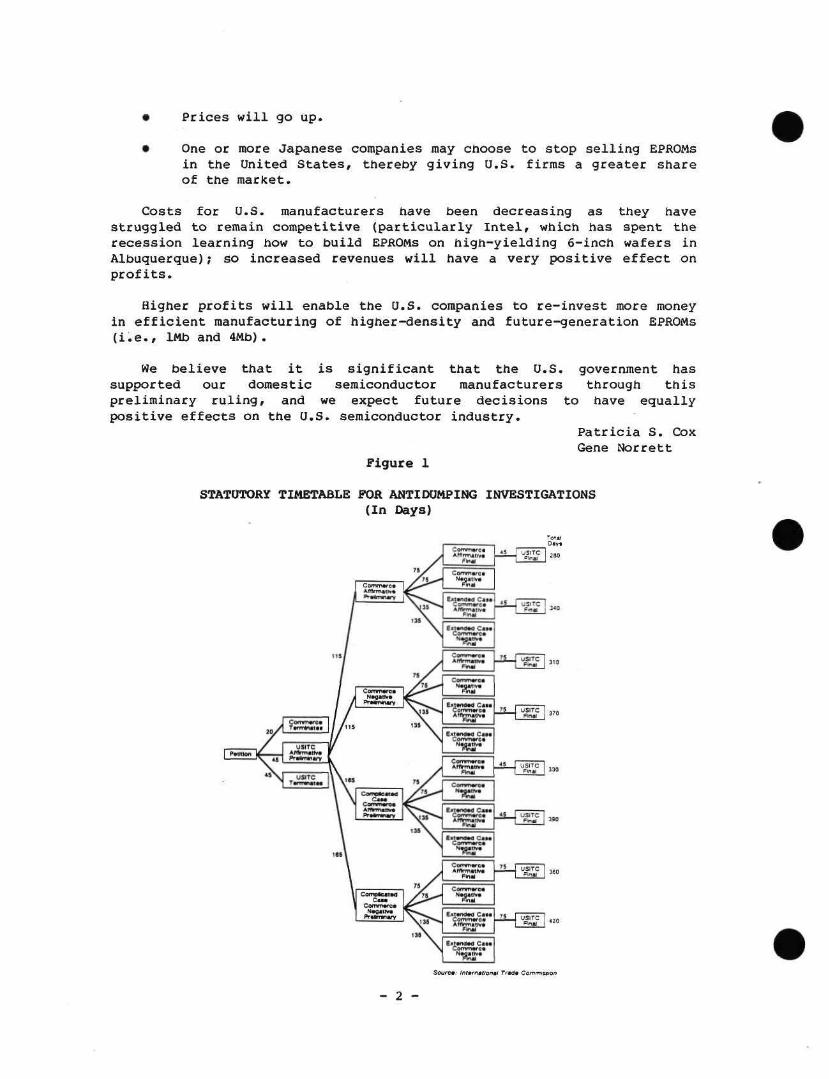
• Prices will go up.
# One or more Japanese companies may choose to stop selling EPROMs in the tJnited States, thereby giving tJ.S. firms a greater share of the market.
Costs for U.S. manufacturers have been decreasing as they have struggled to remain competitive (particularly Intel, which has spent the recession learning how to build EPROMs on high-yielding 6-inch wafers in Albuquerque); so increased revenues will have a very positive effect on profits.
Higher profits will enable the tJ.S. companies to re-invest more money in efficient manufacturing of higher-density and future-generation EPROMs (i.e., 1Mb and 4Mb).
We believe that it is significant that the U.S. government has supported our domestic semiconductor manufacturers through this preliminary ruling, and we expect future decisions to have equally positive effects on the U.S. semiconductor industry.
Patricia S. Cox Gene Norrett
Figure 1
STATUTORY TIMETABLE FOR ANTIDUMPING INVESTIGATIONS (In Days)
Total 0 « ¥ t
A F f l r m t , ^ . p]nu
C o m m . r c . N . o i T r v .
Ext .n4 .cJ C I B * C n m m w c * A m r m . t i v .
Fln.1
COfTVniTH
CofPmmfct AfnrmaUva
F l M i
CDmrnarcB rvHtrtv*
Fhr\|]
EnTHWad C A K C ^ m m a r c * AriWTTutMa 'FM:
EHtVf itftd C i i « C v n m a r c «
N«g«iiw« H n U
Cstnm^fot nmoMttvm
1 ^ 1 ^
E^4O0*d C a i B Cgrmfnafca Afflmaifwa
Pin I t
Ei i tand*d U 4 k * C v T i m a r c *
UmamtHm Fir a^
C j y n r r w E * AHbvrvMrva
Pviai
htagadv* J^M
b T a n d a d C * * * Cffl^rrturca AHlfTMithf*
Pln*l
iLj arnrnar.C Maaattvi
f V i H
*^ I " < l T i ^ ' F ' n H _ |
" i j S i T c l Firm I •
i J$ iTC I . L ^ f 1 * ' _ l •
f^.. I u a i r r 1 ^ inu
Sourcm: tnternatlonal Traaa Commission
- 2 -
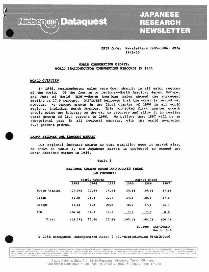
-,t Dataquest -JAPANESE — RESEARCH NEWSLETTER
JSIS Code: N e w s l e t t e r s 1 9 8 5 - 1 9 8 6 , JSIA 1986-15
WORLD CX}tQUHPTION 0P0A7B: WORLD SEHICONIXJCTOR CONStMPTION R^OONOS IN 1986
WORLD OVERVIEW
In 1985, s e m i c o n d u c t o r s a l e s were down s h a r p l y i n a l l major r e g i o n s o f t h e w o r l d . Of the four major r e g i o n s — N o r t h America, Japan , Europe, and R e s t o f World (ROW)—North American s a l e s showed t h e s t r o n g e s t d e c l i n e a t 2 7 . 0 p e r c e n t . DATAQUEST b e l i e v e s t h a t t h e wors t i s b e h i n d u s , however . We e x p e c t growtn in Uie f i r s t q u a r t e r o f 1986 in a l l wor ld r e g i o n s , i n c l u d i n g North America . Th i s p r o j e c t e d f i r s t q u a r t e r growth shou l d p o i n t t n e i n d u s t r y on the way t o r e c o v e r y and a l l o w i t t o r e a l i z e wor ld growtti o f 16 .4 p e r c e n t i n 1986 . We b e l i e v e t h a t 1987 w i l l be an e x c e p t i o n a l year i n a l l r e g i o n a l m a r k e t s , wi th the w o r l d a v e r a g i n g 3 2 . 6 p e r c e n t growth .
JAPAN BECOMES TEE LARGEST MARKET
Our r e g i o n a l f o r e c a s t po in l is to some s t a r t l i n g news in market s i z e . As shown in Tab le 1 , the Japanese market i s p r o j e c t e d t o e x c e e d the North American market i n 1 9 8 6 .
Tab le 1
REGIONAL GROWTH RATES AND MARKET SHARE (In P e r c e n t )
Nor th America
Japan
Europe
ROW
T o t a l
Yeeurlv Growth 1985
(27.0%)
( 2 . 8 )
(3 .6 )
( 1 6 . 6 )
(15.0%)
198 6
10.8%
2 8 . 4
6 . 3
1 4 . 7
16.4%
198 7
34.9%
3 0 . 6
29 .8
3 7 . 1
32.6%
Market Share 1985
38.8%
3 4 . 8
18 .7
7 . 7
100.0%
198 6
36.9%
3 8 . 4
1 7 . 1
7 . 6
100.0%
198 7
37.5%
3 7 . 8
1 6 . 7
8 .0
100.0%
Source: DATAQUEST March 198 6
© 1986 D a t a q u e s t I n c o r p o r a t e d March 7 e d . - R e p r o d u c t i o n P r o h i b i t e d
The content ot this report represents our interpretaion and analysis of information generally available to the public or released by responsible individuals in the subject companies, but is not guaranteed as to accuracy or completeness It does not contain material provided to us in confidence by our clients Individual companies reported on and analyzed by DATAQUEST, may be clients of this and/or other DATAQUEST services This information is not furnished in connection with a sale or offer lo sell securities or in connection with the solicitation of an offer to buy securities This firm and its parent and/or their officers, stockholders, or members of their families may, from time to time, have a long or short
1 i;ar«iiriljpe
Azabu Heights, Suite 711, 1-5-10 Roppongi, MInato-ku, Tokyo 106, Japan 1290 Bidder Park Drive / San Jose, CA 95131 / (408) 971-9000 / Telex 171973
4
The U.S. market i s expected t o picic up scHne share again in 1987, al though i t i s no t expected t o recover i t s former s t a t u s . Note t h a t much of t h e growtih tihat Japan r e a l i z e s in 1986 i s due to currency exchange. Japan ga ins about 19.0 pe rcen t merely from currency exchange because of a s t r eng then ing yen to d o l l a r . Our f o r e c a s t a l s o i n d i c a t e s t h a t European consumption w i l l d e c l i n e as a percentage of the t o t a l between 1985 and 1987. The European market , however, gained cons ide r ab l e market sha re in 1985 r e l a t i v e t o i t s 1984 l e v e l . That market i s a c t u a l l y l e v e l i n g to a normal growtih c y c l e . Our data a l s o i n d i c a t e t h a t tihe ROW region w i l l grow s l i g h t l y t o 8.0 pe rcen t in 1987.
EMD MARKETS KEY ID MARKET STRHtCTHS AND WEAKNESSES
The s e v e r i t y of r e g i o n a l market d e c l i n e s in 1985 was determined l a r g e l y by each r e g i o n ' s end-market focus . The computer /data p rocess ing market was e x c e p t i o n a l l y weak and, consequen t ly , h u r t those markets focusing heav i ly on t h i s a r ea . More s t a b l e were the a p p l i c a t i o n s a reas of consumer e l e c t r o n i c s and te lecommunica t ions .
North America/U.S. Market
With a heavy 40 percent emphasis on computers, the North American market witnessed the most severe decline of all regional markets. The U.S. market noted a sales decline of 27.0 percent. Key to the weakness of the computer market was the computer OEMs' misjudgement of actual consumption. A buying/production cycle was created at the computer level that impacted component suppliers. Inventory in 1984 was accumulated far in excess of actual needs. This inventory is now perceived to be leveling to a more normal volume, which will lead to steady booking and shipment activity. Booking and shipment levels appear to be correcting in many product areas. It is this expectation that points to a 3.9 percent North American market growth in the first quarter of 1986. DATAQUEST believes that normal inventory depletion will continue the quarterly growth pattern through 1986, for a yearly total of 10.8 percent. In 1987, we expect quarterly growth to continue. We believe that 1987 will be a year of strong growth (34.9 percent) in the U.S. market. In terms of levels of consumption, however, it is not until 1987 that we expect consumption to return to the level of 1984.
Japanese Market
The Japanese market was among the more favorable in terms of the 1985 market decline. A heavy emphasis on consumer applications was largely responsible for this stability. DATAQUEST identifies the sales decline in the Japanese market at a modest 2.8 percent in 1985. As stated earlier, we expect the Japanese market to surpass the U.S. market in dollar volume in 1986. The exchange rate is responsible for a good portion of this increase. In yen, the Japanese market is expected to grow about 9.4 percent. Current exchange notes that the U.S. dollar is worth about 203 yen, down significantly from 1985's average of about 237 yen. Our current forecast, incorporating the yen valuation, shows
- 2 -
ttie Japanese market growing 28.4 percent in 1986, far beyond ttie world average of 16.4 percent. In 1987, we expect Japanese market growtti to be on a par witti ttie world, a t 32.6 percent.
European Market
Wit:ti end-^narket focus primarily, in t^e r e l a t i ve ly s table and growing eurea of telecommunications, t:tie European market was not as ser iously affected as ei ther the North American market or ROW market. The European market declined by approximately 3.6 percent in 1985. This modest decl ine allowed Europe to pick up market share r e l a t i v e to the world in 1985. I t is expected, however, that th is market share wi l l rever t to i t s normal level of about 16.6 percent (in 1984) of t o t a l s a l e s . Note that Table 1 overstates Europe's market share because Europe gained over 2.0 percentage points in tot:al market s i ze in 1985. The decline in t o t a l percentage shotm for years 1986 and 1987 brings Europe back to i t s 1984 market share of 16.6 percent.
ROW Market
The ROW region, l ike the Japanese market, focuses primarily on consumer-oriented products, a market that was r e l a t i v e l y s table in 1985. Yet t:he ROW region also sees a large amount of a c t i v i t y from foreign and North American companies building ccanputer equipment abroad. I t is the balance of these factors that caused a market decline of 16.6 percent in 1985. As in other regions, we expect quar ter ly growth to be effect ive throughout 1986 and 1987. DATAQUEST projects ROW growth at 14.7 percent in 1986 and 37.3 percent in 1987.
WORLD PROPqCT TRENDS
In our quar ter ly world product forecast shown in Table 2, we project that MOS products wil l mcike a ccnneback in 1986. MOS and bipolar d ig i t a l were the areas most strongly affected in 1985; both were down approximately 21 percent. The product area that noted the s t rongest decl ine , however, was MOS memory, which dropped about 36.3 percent worldwide. In this memory area, s teep quar ter ly grow1:h i s required to pul l i t up from i t s 1985 trench. We believe that th is growth is r e a l i s t i c and forecast that MOS memory wi l l be up 12.0 percent in 1986. MOS microprocessor devices and MOS logic are also expected to show good growth that wil l continue to build momentum into 1987. Our estimated MOS technology growth in 1987 is a lofty 49.5 percent, raised through high recovery expectations for MOS memory and MOS micro devices. Bipolar products are also projected for growth, but they are not as dramatic in percentage terms as MOS d i g i t a l products. Other product areas of l i nea r , d i s c r e t e , and optoelectronics tihat did not decline severely in 1985 are not expected to ramp up as quickly as harder h i t product areas .
Patr ic ia S. Cox Barbara A. Van Howard 2. Sogert
- 3 -
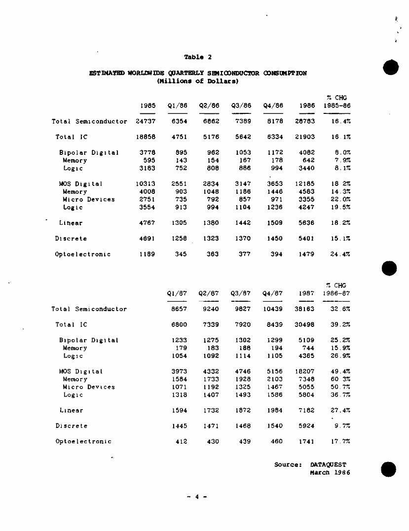
Table 2
ESTIMATED WORLDWIDE QUARTERLY SQIICONDUCTOR CONSQMPTION ( M i l l i o n s o f D o l l a r s )
'otal Semiconductor
Total IC
Bipolar Digital Memory Logic
MOS Digital Memory Micro Devices Logic
Linear
Discrete
Optoelectronic
1985
24737
18858
3778 595
3183
10313 4008 2751 3554
4767
4691
1189
Ql/86
6354
4751
895 143 752
2551 903 735 913
1305
1258
345
Q2/86
6862
5176
962 154 808
2834 1048 792 994
1380
1323
363
Q3/86
7389
5642
1053 167 886
3147 1186 857 1104
1442
1370
377
Q4/86
8178
6334
1172 178 994
3653 1446 971 1236
1509
1450
394
1986
28783
21903
4082 642 3440
12185 4583 3355 4247
5636
5401
1479
% CHG 1985-86
16.4%
16. 1%
6.0% 7.9% 8 . 1%
18 2% 14.3% 22.0% 19.5%
18.2%
15 . 1%
24.4%
Total Semiconductor
Total IC
Bipolar Digital
Memory Logic
MOS Digital Memory
Micro Devices Log 1 c
Linear
Discrete
Optoelectronic
Ql/87
8657
6800
1233 179
1054
3973
1584 1071
1318
1594
1445
412
Q2/87
9240
7339
1275 183
1092
4332 1733 1192 1407
1732
1471
430
Q3/87
9827
7920
1302 188 1114
4746 1928 1325 1493
1872
1468
439
Q4/87
10439
8439
1299 194
1105
5156 2103 1467 1586
1984
1540
460
1987
38163
30498
5109 744
4365
18207 7348 5055 5804
7182
5924
1741
% CHG 1986-87
32.6%
39.2%
25.2% 15.9% 26.9%
49,4% 60 3% 50 . 7%
36. 7%
27,4%
9.7%
17,7%
S o u r c e : DATAQUEST Marcti 198 6
- 4 -
Dataquest 1,1 I f n m i M l l ; l i l \ l 11;- I 'U (IT (Mtt ;i I ic I11
RESEABCK BULLETIN
JSIS Code: Newsle t t e r s 1985-1986, JSIA 1986-17
MEGACELL FEVER: JAPANESE DEVELOPING AUTOMATED STANDARD CELL SYSTEMS
StJMMARY
Automated m e g a c e l l t e c h n o l o g y — t h e wave of t h e f u t u r e ? J a p a n e s e v e n d o r s have l e a p e d i n t o t h e s t a n d a r d c e l l ma rke t and a r e now i n t r o d u c i n g m e g a c e l l s and d e s i g n a u t o m a t i o n s y s t e m s . In March, . H a t s u s h i t a announced i t s S t a n d a r d Layout Design Automat ion System (STELLA), which r u n s on a VAX and i s c a p a b l e of h a n d l i n g up t o 30 ,000 g a t e s . x^datsushi ta , which f o l l o w s F u j i t s u and NEC in i n t r o d u c i n g ASIC d e s i g n a u t o m a t i o n t o o l s , o f f e r s 200 c e l l s in i t s s t a n d a r d c e l l l i b r a r y .
As shown in Tab le 1 , DATAQUEST e s t i m a t e s wor ldwide merchan t consumpt ion of s t a n d a r d c e l l s t o grow from $246 .3 m i l l i o n in 1985 to 3 4 . 0 b i l l i o n in 1990 , r e p r e s e n t i n g 20 p e r c e n t o f t o t a l ASIC consumpt ion and 10 p e r c e n t o f t o t a l s e m i c o n d u c t o r consumpt ion in 1 9 9 0 .
J a p a n e s e companies a r e r u s h i n g t o d e v e l o p s t a n d a r d c e l l l i b r a r i e s i n c o r p o r a t i n g s t a n d a r d RAMs, ROMs, EPROMs, EEPROMs, and MPUs. "Smar t" VTRs, h i g h - r e s o l u t i o n t e l e v i s i o n s e t s , and IC c a r d s a r e c u r r e n t l y h o t end u s e s . Tab le 2 summarizes J a p a n e s e s t a n d a r d c e l l d e v e l o p n e n t a c t i v i t i e s .
STRATEGIC IMPLICATIONS
DATAQUEST b e l i e v e s t h a t ASIC makers must d e v e l o p s t a n d a r d c e l l and m e g a c e l l t e c h n o l o g y t o remain c o m p e t i t i v e w i t h J a p a n e s e v e n d o r s . As d i s c u s s e d in our r e c e n t n e w s l e t t e r , "How t o Succeed in ASICs , " d a t e d F e b r u a r y 14 , 1986, ASIC makers must d e v e l o p s u b - 1 . 5 - m i c r o n CMOS t e c h n o l o g y , au toma ted CAD s o f t w a r e , au toma ted m a n u f a c t u r i n g and i n v e n t o r y c o n t r o l , and s t r o n g s e r v i c e s u p p o r t . E x c e l l e n t s e r v i c e , f u n c t i o n a l i t y , u s e r - f r i e n d l y s o f t w a r e , and a u t o m a t i o n w i l l s e p a r a t e t h e w i n n e r s from t h e l o s e r s in t h i s c o m p e t i t i v e f i e l d .
S h e r i d a n T a t s u n o
198 6 D a t a q u e s t I n c o r p o r a t e d March 6 e d . - R e p r o d u c t i o n P r o h i b i t e d
The content ol Itiis report represenls our inlerpretalion and analysis ol tnlormaiIon generally available to Ihe public or released by responsible individuals in the subject companies bul is not guaranteed as lo accuracy or cornpleleness II does not contain
material provided to us m conlidence by our clients IndivIdual companies reported on and analyzed by [y'.TAQUEST may be clients ot Ihis and/or oitier DATAQUEST services Ttiis intormation is not furnished m connection with a sale or otfer to sell securities
or m conneaion with the sdicitalion of an offer to buy securities This firm and its parent and/or ther officers stockholders or members of their families may Irom bme to time have a long or sfiort position in the secunlies menlioned ana may sen or txjy sucn securities L Dataquest Incorporated, 1290 Ridder Park Drive, San Jose, CA 95131-2398, (408) 971-9000, Telex 171973
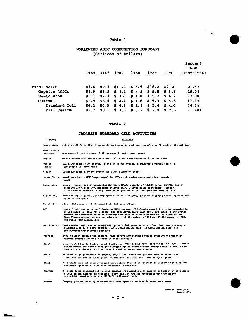
Table 1
WORLDWIDE ASIC CONSUMPTION FORECAST ( B i l l i o n s of Dollars)
1985 1986 1987 1988 1989 1990
P e r c e n t CAGR
(1985-1990)
T o t a l ASICs C a p t i v e ASICs Semicustom Custom
S t a n d a r d C e l l Ful'* Custom
$7 .6 $ 9 . 3 $ 1 1 . 3 $13 .5 $ 1 6 . 2 $20 .0 21.5% $ 3 . 0 $ 3 . 5 $ 4 . 1 $ 4 . 9 $ 5 . 8 $ 6 . 8 18.0% $1 .7 $ 2 . 3 $ 3.0 $ 4.0 $ 5 .2 $ 6.7 32.3% $ 2 . 9 $ 3 . 5 $ 4 . 1 $ 4 .6 $ 5 . 3 $ 6 .5 17.1% $ 0 . 2 $ 0 . 5 $ 0 .8 $ 1.4 $ 2 . 4 $ 4.0 74.3% $ 2 . 7 $ 3 . 1 $ 3 .3 $ 3 .2 $ 2 . 9 $ 2 . 5 (1.4%)
Table 2
JAPANESE STANDARD CELL ACTIVITIES
A c t i v i t y
S e i l i n q VLSt T p c n n o l o q y ' s m e q a c e l l s in J a p a n ; i n i t i a l year t a c q e t e d a t » 1 b i l l i o n (S5 m i l l i o n )
Oeveiopinq 2 - and 1-micron CMOS p r o c e s s ; I - and 2 - i a y e r meta l
CMOS s t a n d a r d c e l l l i b r a r y w i t h over 100 c e l l s ; g a t e d e l a y s o f 2 .1ns pec g a t e
Rece iv ing o r d e r s w i t n F \ j j l t 3 u : p l a n s t o t r i p l e o v e r a l l technology d i v i s i o n s t a f f t o LOO people in t t icee y e a r s
Automat ic f l o o r - p l a n n i n g s y s t e n for blocK p lacement phase
Developing 1 6 - b i t MCU " s u p e r c h i p s * for VTRs, t e l e v i s i o n s e t s , and o t t i e r consisner
goods
S tandard l a y o u t Design Automat ion System (STBLLA) c a p a b l e o f JO,000 g a t e s f nN72000 S e r i e s o f f e r i n g 2 .0 - f l i i c ron OiOS p r o c e s s ; 1 - l a y e r p o l y , 2 - l a y e r m e t a l t e c h n o l o g y ; l i b r a r y Of 200 c e l l s ) o r d e r s from Hay 1986 ; s a l e s g o a l o f v? b i l l i o n (S40 m i l l i o n ) i n 1986
fMOS 6 0 0 - c e l l l i D r a r y « p l u s CAD system; u s i n g a B i - O I O S , JHRlcron b u i l d i n g blocK approach f o r up t o 24 ,000 g a t e s
Adding CAD systems for s t a n d a r d c e l l s and g a t e a r r a y s
Standard c e l l s e r i e s u s i n g l . S n i i c r o n (MOS p r o c e s s ; 1 7 , 0 0 0 - g a t e c a p a b i l i t y t o b« expanded t o 25 ,000 g a t e s i n 1 9 8 6 ; VlO m i l l i o n ($S0 ,000 ) deve lopment c o s t Coc J , 0 0 0 g a t e s ; a CAD system (LQHBO) t h a t c o n v e r t s c i r c u i t s d i r e c t l y from p r i n t e d c i r c u i t boards t o LSI c i r c u i t s f o r 200,UOO-gate b l o c k s ; a c c e p t i n g o r d e r s up t o 1 7 , 0 0 0 g a t e s i n 198S and 2 5 , 0 0 0 g a t e s in 1 9 8 6 ; 300 c e l l s (140 m a c r o c e l l s )
OK i K l e c t r l c OtOS s t a n d a r d c e l l s e r i e s (ftSN91000) up t o 2 4 , 0 0 0 g a t e s u s i n g a 1 .5ns» 2 - 4 l c r o n p r o c e s s ; a s t a n d a r d c e l l J 2 - b l t MPU (HVM6971) on a 224ffl«-square c h i p ; 12-month d e s i g n t i m e ; s i x IBM PC-based CAD s o f t w a r e packages
P i o n e e r CMOS 1-micron process f o r i n t e r n a l g a t e a r r a y s and s t a n d a r d c e l l s ; e n t e r i n g t h e merchant marke t ; adding f i v e t o s i x r e s e a r c h s t a f f a n n u a l l y
Ricoh A new metnod for d e s i g n i n g c u s t o a s i n g l e - c h i p HCUs around R o c k w e l l ' s 8 - b i t OiOB nCU; a conmon
design method for g a t e a r r a y s and s t a n d a r d c e l l s ; added Western Design C e n t e r ' s 1 6 - b l t CPU c o r e t o c e l l l i b r a r y (6SC816) j over ISO c e l l s , up t o 10 ,000 g a t e s
Sanyo s t a n d a r d c e l l s i n c o r p o r a t i n g LC9500, TTL74 , and LC9500 s e r i e s ; NRS c o a t o f ¥4 m i l l i o n
(S16 ,000 ) f o r 500 t o 1 ,000 g a t e s ; V6 m i l l i o n ( 4 2 4 , 0 0 0 ) f o r J , 0 0 0 t o 4 , 0 0 0 g a t e s
Comp^n;^
A.<4ani Glass
Asjhi Micro-Systems
PU] i t s u
Fu] i t s u ausho
H i t a c n i
Japan V i c t o r
Matsu .sh i ta
M i t s u b i s h i
Ninon LSI
NEC
Sharp A s t a n d a r d c e i l c o r r e c t i o n program t h a t a l l o w s changes i n p o s i t i o n o f e lements a f t e r w i r i n g has begun; p o t e n t i a l 10 p e r c e n t r e d u c t i o n I n c h i p s i s e
A t r i p l e - l a y e r s t a n d a r d c e l l w i r i n g program t h a t p e r m i t s a 10 p e r c e n t r e d u c t i o n in c h i p s i z e ; a CMOS s e r i e s capab le o f mount ing 4R RAN and 16K ROM and c c a p a t i b X e w i t h T o s h i b a ' s u l t r a - n i g h speed g a t e a r r a y s (1C22SC) ; Z80-based c e l l s
Company g o a l o f r e d u c i n g s t a n d a r d c e l l development t ime f r o a 20 weeks t o 6 weeks
S o u r c e : OATAQUBST March 198 6
- 2 -
Dataquest Lititini'Kfrtviil llli'PiIIi;M1I:iilstIiitILiiI|'<ii;itHt)i
ESEARCH BULLETIN
J S I S Code: N e w s l e t t e r s 1985-1986 , JSIA 1986-16
JAPAN FOSatS NBff JUJTQHOTIVE MATERIALS RESB^^CH PROJECT
SCIMMARY
T w e n t y - f i v e J a p a n e s e companies r e c e n t l y formed t h e Next G e n e r a t i o n New A l l o y s R e s e a r c h A s s o c i a t i o n t o d e v e l o p new a u t o m o t i v e m a t e r i a l s . S p o n s o r e d by Totioku U n i v e r s i t y ' s E n g i n e e r i n g Depar tment and t h e M e t a l l u r g y R e s e a r c h Associa t icHi in S e i d a i C i t y ( n o r t h of T c ^ y o ) , t h e new j o i n t R&D p r o j e c t i n v o l v e s e i g h t a u t o m o b i l e makers ( i n c l u d i n g Toyot:a and N i s s a n ) , s i x s e m i c o n d u c t o r companies (NEC, H i t a c h i , and o t h e r s ) , and e l e v e n m a t e r i a l s c o m p a n i e s . The r e s e a r c h c o n s o r t i u m w i l l d e v e l o p a l l o y s for t h e p a r t i c i p a t i n g c a r m a k e r s , f o c u s i n g on four a r e a s :
• Amorphous a l l o y s
• Shaped memory a l l o y s
• F i n e c e r a m i c s (car e n g i n e s and IC p a c k a g i n g )
• Hydrogen s t o r a g e a l l o y s
The Aoba E n g i n e e r i n g Promot ion A s s o c i a t i o n w i l l i n v e s t i g a t e t h e t e l e c o m m u n i c a t i o n s and n u c l e a r power a p p l i c a t i o n s o f t h e s e new a l l o y s .
DATAQDEST ANALYSIS
J a p a n e s e a u t o m o t i v e companies a r e r a p i d l y p u s h i n g i n t o e l e c t r o n i c s and new m a t e r i a l s t o d e v e l o p l i g h t e r , s t u ronge r , and I C - i n t e n s i v e c a r s . DATAQUEST e s t i m a t e s t h a t J a p a n e s e a u t o m o b i l e makers consumed ¥72 b i l l i o n ($303 m i l l i o n ) wor th o f s e m i c o n d u c t o r s i n 1 9 8 5 , which w i l l grow 16 p e r c e n t t o 5f83.5 b i l l i o n ($464 m i l l i o n ) i n 1 9 8 6 . In c o m p a r i s o n , e s t i m a t e d U . S . a u t o m o t i v e s e m i c o n d u c t o r consumpt ion was abou t $800 m i l l i o n in 1 9 8 5 , which w i l l grow t o $ 1 . 2 b i l l i o n by 1 9 8 9 .
As shown in Tab le 1 , Honda, Mazda, N i s s a n , and Toyota a r e e n l a r g i n g t h e i r e l e c t r o n i c r e s e a r c h c e n t e r s , e x p a n d i n g IC p r o d u c t i o n , and p u r c h a s i n g s u p e r c o m p u t e r s for a u t o m o t i v e d e s i g n . Nippondenso , a major I b y o t a s u p p l i e r , i s b u i l d i n g a new $160 m i l l i o n p l a n t ; Nippon Denso (a d i f f e r e n t company) opened a r e s e a r c h o f f i c e in M i c h i g a n .
© 1986 D a t a q u e s t I n c o r p o r a t e d March 5 e d . - R e p r o d u c t i o n P r o h i b i t e d
The conlent ot this lepor! represents our InterprelalIon and analysis Ql intormation generally available to the public or released by responsIble individuals in the sub|eci companIes but is not guaranteed as to accuracy or completeness II does not contain
material orovIded to us m conlIdence bv our clients Individual companies reported on and analyzed by QftTAQUEST may be clIerts of this and/or other DATAQUEST servIces This Information Is not furnished m connection with a sale or otier to sell securities
nr in conneciIon wIth the sdIcitation o( an ofler to Ixjy gecuntIes This firm and its parent and/or their officers slocl hIDlde's or members ot theIr families may, from bme to time ha\« a long or short posItion in Itie secunttes mentioned and may sell or buy such secuntIes
Dataquest Incorporated, 1290 Ridder Park Drive, San Jose, CA 95131-2398, (408) 971-9000, Telex 171973
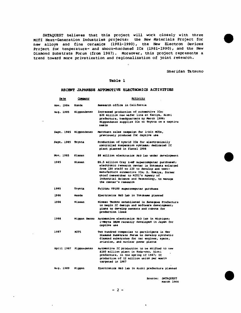
DATAQUEST be l ieves tha t t h i s projec t w i l l work c l o s e l y with three MITI Next-Generation Indus tr ies p r o j e c t s : the New Ma ter ia ls P rojec t for new a l loy s and f ine ceramics (1981-1990), the New Elec t ron Devices Projec t for tempera ture- and shock-hardened ICs (1981-1990), and the New Diamond Subs t ra te Porum (fran 1987) . Moreover, t h i s p rojec t rep r e sen t s a t rend toward more p r i v a t i z a t i o n and reg iona l iza t ion of j o i n t resea rch .
S h e r i d a n Tatrsuno
Table 1
RECENT JAPANESE AUTQHOTIVE BI£CTRDNICS ACTIVITIES
Date Conpany
Nov . 1984 Honda
Aug . l a a s Nippondenso
S e p t . 198S Nippondenso
S e p t . 1983 Toyota
Nov . 1985 N i s s a n
1985 N i s s a n
1985
1986
Toyota
Mazda
A c t i v i t y
R e s e a r c a o f f i c e i n C a l i f o r n i a
I n c r e a s e d p r o d u c t i o n o f a u t o m o t i v e ICs; $20 m i l l i o n new wafer l i n e a t K a r i y a , A ic t i i p r e f e c t u r e , h e a d q u a r t e r s t>y Harcti 1986; Nippondenso s u p p l i e s ICs t o Obyota on a c a p t i v e o a s i s
Merchant s a l e s campaign for l - b i t MCUs, p r e v i o u s l y produced for c a p t i v e u s e
P r o d u c t i o n o f n y b r i d ICs for e l e c t r o n i c a l l y c o n t r o l l e d s u s p e n s i o n s y s t e m s ; d e d i c a t e d IC p l a n t p lanned in f i s c a l 1986
$8 m i l l i o n e l e c t r o n i c s fUO lat> under deve lopment
3 6 . S m i l l i o n Cray X-MP supercomputer p u r c h a s e d ; e l e c t r o n i c r e s e a r c h c e n t e r in Ifokosuka e n l a r g e d from ISO s t a f f t o 220 t o d e v e l o p and t e s t -manufac ture a u t o m o t i v e ICs; S . Romiya , former c h i e f r e s e a r c h e r t o MITI's Agency o f I n d u s t r i a l S c i e n c e and T e c h n o l o g y , t o manage the c e n t e r ' s r e s e a r c h
F u j i t s u VPIOO superccxnputer p u r c h a s e
e l e c t r o n i c s RftO Lab i n YoItonama p lanned
1986 N i s s a n N i s s a n Techno e s t a b l i s h e d i n Kanagawa P r e f e c t u r e t o b e g i n IC d e s i g n and s o f t w a r e d e v e l o p m e n t ; p l a n a t o d e v e l o p s e n s o r s and r o b o t s f o r p r o d u c t i o n l i n e s
1986 Nippon Oenso Automot ive e l e c t r o n i c s RtO l a b in Mich igan; l-ftt>yte ORAM r e c e n t l y d e v e l o p e d i n Japan f o r c a p t i v e u s e
1987 MITI
A p r i l 1987 Nippondenso
Aug . 1989 Nippon
Two hundred companies t o p a r t i c i p a t e in New Diamond S u b s t r a t e Porum t o d e v e l o p s y n t h e t i c diamond s u b s t r a t e s f o r car e n g i n e s , s p a c e , a v i a t i o n , and n u c l e a r power p l a n t s
Automot ive IC p r o d u c t i o n t o be s h i f t e d t o new $160 m i l l i o n p l a n t in Koda -cho , A i c h i p r e f e c t u r e , i n t h e s p r i n g o f 1987; IC p r o d u c t i o n o f 12 m i l l i o n u n i t s per month t a r g e t e d i n 1987
E l e c t r o n i c s RtO l a b in A i c h i p r e f e c t u r e planned
S o u r c e : DATAQUEST March 198 6
- 2 -
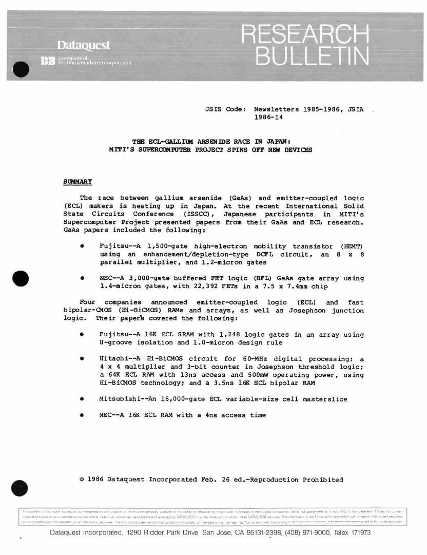
Dataquest :i(i]ni|i-irL\ til
tESEARCK BULLETIN
JS IS Code: N e w s l e t t e r s 1985 -1986 , JSIA 1986-14
TOB BCL-GALLim ABSEHIDE RACE IN JAPAN; M I T I ' S SUPEROOMFOTER PROJECT SPINS OFF NEW DEVICES
StMMARY
The r a c e be tween g a l l i u m a r s e n i d e (GaAs) and e m i t t e r - c o u p l e d l o g i c (BCD makers i s h e a t i n g up i n J a p a n . At t h e r e c e n t I n t e r n a t i o n a l S o l i d S t a t e C i r c u i t s C o n f e r e n c e (ISSCC), J a p a n e s e p a r t i c i p a n t : s in M I T I ' s Supercompute r P r o j e c t p r e s e n t e d p a p e r s from t h e i r GaAs and ECL r e s e a r c h . GaAs p a p e r s i n c l u d e d t h e f o l l o w i n g :
• Fuji tsu—^A 1 , 5 0 0 - g a t e h i g h - e l e c t r o n m o b i l i t y t r a n s i s t o r (HEMT) u s i n g an e n h a n c e m e n t / d e p l e t i o n - t y p e DCFL c i r c u i t , an 8 x 8 p a r a l l e l m u l t i p l i e r , and 1.2-micrc»i g a t e s
• NEC~A 3 , 0 0 0 - g a t e b u f f e r e d FET l o g i c (BFL) GaAs g a t e a r r a y u s i n g 1 . 4 - m i c r o n g a t e s , w i t h 22 ,392 FETs in a 7 .5 x 7.4mm c h i p
Pour compan ies announced e m i t t e r - c o u p l e d l o g i c (ECL) and f a s t bipolar-CMOS (Hi-BiCMOS) RAMs and a r r a y s , a s w e l l a s J o s e p h s o n j u n c t i o n l o g i c . T h e i r paper ' s c o v e r e d t h e f o l l o w i n g :
• Fuji tsu—^A 16K ECL SRAM w i t h 1,248 l o g i c g a t e s in an a r r a y u s i n g U-groove i s o l a t i o n and 1 . 0 - m i c r o n d e s i g n r u l e
• Hitachi—^A Hi-BiCMOS c i r c u i t f o r 60-MHz d i g i t a l p r o c e s s i n g ; a 4 x 4 m u l t i p l i e r and 3 - b i t c o u n t e r i n J o s e p h s o n t h r e s h o l d l o g i c ; a 64K ECL RAM w i t h 13ns a c c e s s and 500mW o p e r a t i n g power , u s i n g Hi-BiCMOS t e c h n o l o g y ; and a 3 . 5 n s 16K ECL b i p o l a r RAM
• Mitsubishi—^An 1 8 , 0 0 0 - g a t e ECL v a r i a b l e - s i z e c e l l m a s t e r s l i c e
• NEC—A 16K ECL RAM w i t h a 4ns a c c e s s t ime
© 1986 D a t a q u e s t I n c o r p o r a t e d F e b . 26 e d . - R e p r o d u c t i o n P r o h i b i t e d
The content ol this repon represents our Interpretation and analy^Is of intornnatIon gene'ally available to It e puOiC or released by responsible indIviduals m the subiecl companIes but Is nol guaranteed as to accuracy or completeness 11 does not contain
maienal provided to us In contidence by our clIenls Individual companies repIarted on and analyzed by DATAQUEST may be clIenls ol this and/or ottier DATAQUEST servIces ThIs Information Is not furnished m connection with a sale or otter to sen securIlIes
01 in connectIon with the solIcIiaiIOn oi an oner lo Duy securmes inIs iirm ana us parent ana/or ineif onicers siIjcKnoIuerb ur IneInuetb uI IIIIiir ictIniIIe j Indy fium ume *iO lime have 5 lor,g or shot pC3'',.C' r tt'C z^^^ir'-'i". ""j"';?"?'?^ ^ r? •^^v "^'i <^' '^•'" surn <;p<~iiriMPc
Dataquest Incorporated, 1290 Ridder Park Drive, San Jose, CA 95131-2398, (408) 971-9000, Telex 171973
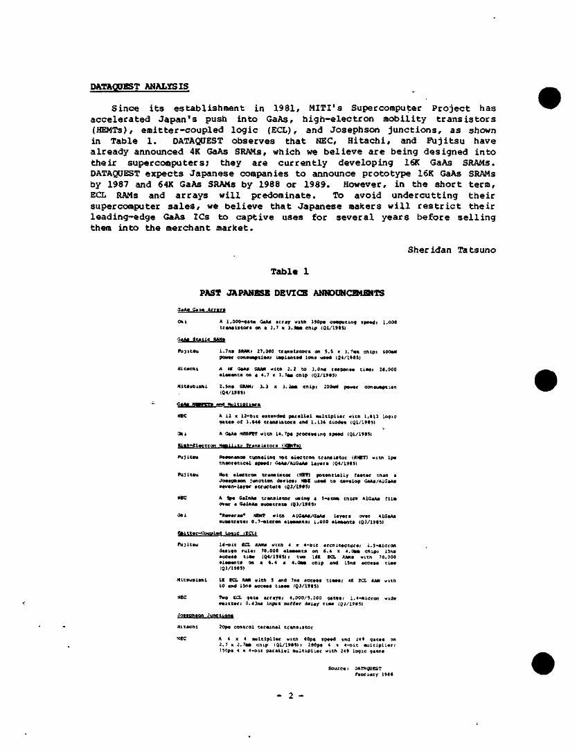
DATAQDEST ANALYSIS
Since i t s es tab l i shment in 1981, MITI's Supercomputer P ro jec t has acce l e r a t ed J a p a n ' s push in to GaAs, h i g h - e l e c t r o n mobi l i ty t r a n s i s t o r s (HEMTs), emi t t e r - coup led l o g i c (ECL), and Josephson j u n c t i o n s , a s shown in Table 1. DATAQUEST observes t h a t NEC, H i t a c h i , and Fu j i t su have a l ready announced 4K GaAs SRAMs, which we b e l i e v e a re being designed in to t h e i r supercomputers; they are c u r r e n t l y developing 16K GaAs SRAMs. DATAQUEST expects Japanese companies to announce prototype 16K GaAs SRAMs by 1987 eind 64K GaAs SRAMs by 1988 or 1989. However, in the sho r t term, ECL RAMs and a r r a y s w i l l predominate. To avoid undercu t t ing t h e i r supercomputer s a l e s , we be l i eve t:hat Japanese malcers w i l l r e s t r i c t t h e i r leading-edge GaAs ICs to cap t ive uses for s eve ra l yea r s before s e l l i n g them in to the merchant market.
Table 1
PAST JAPANESE DBVICB ANNOUNCQIBITS
G j A i G a M Acrav»
Oki A l ,a00-qst<i OiAj a r r a y w i t h 390ps coiiputtn<3 ap**dt 1,000 t c a n s i s e o f i on a J.7 K 3.9aa cnip (QI /19aS)
GaAa S t a t i c RAMa
F u j i t s u I>7na SRMi 27,000 c r a n a i s t o r s on 5.S x 3.7nii cntp j SOOaH PCM9S cwiauftptioni iaplanead ions osad 0 4 / 1 9 8 5 )
UicachL A 4K OaAa SRJW w i t n 2 .2 to 3.0ns ccsponsa t inwt 29.000 • l a « « n t a on a 4.7 x 3.7aa cfi ip {g2/19aS)
M i t s u b i s h i 2.Sns SRAMi 3.3 X 3 .2«a c h i p ; 200iiH powar consuaption (Q4/198S)
CaAj H f era m d H u l t i p l i w a
NIC A 12 X I 2 - 0 i t axtandad p a c a l l a l n u l t i p l i a r w i th L.813 Loqlc 9«taa at 3,S46 cranaistocs and 1,136 diodas (Ql /1985)
Om A OaAs NBSPer w i t h i 4 .7ps proevssinq sp»ad (Ql /1985)
m q n - g l a c t c m Kcaoii it^ ? f a i T a i a t « s jKWtTsl
Pu j ieau Raaonanc* tunna i inq not a i a c t i o n eranaiatoc (RHET) wicn Ips t h a o e a t i c a i spawli aaAs/Aia«Aa l a y a r a (Q4/ I983)
^ j i t s u Hot a i a e t r o n t r ana is to t (HET) p o t a n t i a l l y Caster than a Joaaphaon Junction dav ica i HBE usad to davalop GaAa/AlGaAs savan-Layac secuctuca (Q3/L98SI
NEC A Spa OaloAa t ranaiscec uainq a S-atoa t h i c k AlOaAa f i l a ovar a GaXnAs suoaeraea (03 /1985)
OKi ' R a v a r a * ' HEiiT w i t h ALGaAa/GaAa l a y a r s ovar AIGaAa auba t ra ta i 0 . 7 * « i c r a n a laaants t l.OOO a l .a«mta (gj /19f l5}
e*tt.tar-Co^iil«t<. Logic |ECL>
P u j i t a u I S - o i t ECI. RAMa w i t h 4 x 4 - b i t a r c t i i t a c t u r a ; l . S - n i c r o n daaiqn eu la i 70,000 a iaaanta on 6.4 x 4.0aa chLpi ISns accass tLsa (Q4/198S) ; two ISR SCL RAMa wi th 70.000 • l a a a n t a on a 6.4 x 4.0Ma cn ip and ISns accasa t i a a {Q3/I98S)
M i t a u b i a h i IR BCL RAM with S and 7ns accasa t i n a a j 4K BO. RAM with 10 and ISns accaaa t i a a a (Q3/198S)
NEC Two SCZ. 9a ta a r r a y s ; 4,000/5.1300 ga tas ; I . .4 -n icron wida e « i t t a r ; 0.43na input ou££ar da lay t i n a (Q3/L98S)
Josaphson Junct iona
H i t a c h i 20pa c o n t r o l t a r a i n a l t r a n s i s t o r
NBC A 4 X 4 a u l t i p i i a r w i th 80pa spaad and 249 gatas on 2.7 X 2 .7aa chip ( Q l / 1 9 8 5 ) ; 2aOpa 4 x 4 - o i t n u i t i p L i a r : 35aps 4 X 4-t>it p a r a i i a i a u i t i p l i e r w i th 249 Loqtc •^ates
Souica: DATAQUEST Pabruary 1986
Sheridan Tatsuno
- 2 -
Dataquest JAPANESE RESEARCH NEWSLETTER
JSIS Code: News le t t e r s , 1985-1986 1986-12
1985 JAPAN CAD/CAM USER SURVEY
StUMARY
DATAQUEST recently completed its first annual CAD/CAM end-user survey in Japan. The purpose of the survey was to gain insight from users currently using CAD/CAM systems. The survey questions closely paralleled those asked in DATAQUEST's U.S. survey administered early in 1985 (see DATAQUEST's CCIS newsletter No. 84 entitled, "1985 CAD/CAM User Survey Results") and was designed to detect similarities and differences in the two geographical regions.
DATAQUEST surveyed end users using products from the following CAD/CAM vendors in Japan:
C. Itoh Data Systems (U.S. affiliation: Calma)
Cadam
Applicon, Ecad, Zycad)
F u j i t s u
Marubeni Itytech (U.S. a f f i l i a t i o n ;
Mentor Graphics
NEC
Sekio Instruments & Electronics (U.S. affiliation: Systems, McAuto, Zuken)
Technodia (U.S. affiliation: Valid Logic)
Tokyo Electron (U.S. affiliation: Computervision)
Toshiba
Daisy
© 1986 Dataquest Incorporated Feb. 14 ed.-Reproduction Prohibited
The content ot Itiis report represents our interpretaion and analysis of informaiion generally available to the public or released by responsible individuals in the subject companies, but is not guaranteed as to accuracy or completeness It does not contain material provided to us in confidence by our cIients Individual companies reported on and analyzed by DATAQUEST, may be clients ol this and/or other DATAQUEST services This information is not furnished in connection with a sale or ofler to sell securities or in connection with the solicitation of an offer to buy securities This firm and its parent and/or their officers, stockholders, or members of their families may, from time to time, have a long or short Dosition in the securities mentioned and may sell or buy such securities
Azabu Heights, Suite 711, 1-5-10 Roppongi, Minato-ku, Tokyo 106, Japan 1290 Bidder Park Drive / San Jose, CA 95131 / (408) 971-9000 / Telex 171973
In 1984, these ten vendors accounted for $441 million in Japanese CAD/CAM revenue (60 percent of total 1984 Japanese CAD/CAM revenue) and 3,685 installed 1984 total workstations shipped in Japan (48 percent of total installed Japanese workstations).
The 1,200 questionnaires were mailed to the CAD/CAM system managers at these installations (sites), and 397 (33 percent) were returned and used in compiling the results. The sum of the workstations at these sites totalled 4,644 units.
SURVEY FOODS
DATAQUEST chose the following five major issues as the focus of this survey:
• Survey demographics—By industry classification, by type of applications, and by system usage
• Penetration—Number of workstations installed, percentage of trained users, trained users per workstation, number of engineers and draftsmen per site, engineers and draftsmen per workstation, the use of standalone workstations, and the use of color workstations
• Personal computer use in CAD/CAM
• Pricing expectations for workstations relative to the following parameters: main memory, disk storage, screen resolution, screen size, and preference for either color or monochrome screen
• Solids modeling in CAD/CAM
SURVEY DEMOGRAPHICS
Industry Classification
Those surveyed were asked to identify the one industry classification from the following list that best described the type business in which their company was engaged:
• Aerospace
• Architecture/building
• Automotive
• Chemical and a l l ied products
- 2 -
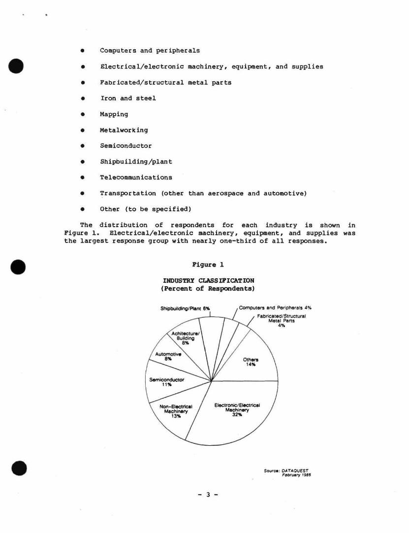
Computers and peripherals
Electrical/electronic machinery, equipment, and supplies
Fabricated/structural metal parts
Iron and steel
Mapping
Metalworking
Semiconductor
Shipbuilding/plant
Telecommunications
Transportation (other than aerospace and automotive)
Other (to be specified)
The distribution of respondents for each industry is shown in Figure 1. Electrical/electronic machinery, equipment, and supplies was the largest response group with nearly one-third of all responses.
Figure 1
INDUSTRY CLASSIFICATION (Percent of Respondents)
Shipbuilding/Plant 6% Computers and Peripherals 4%
Fabricated/Structural Metal Parts
4%
Sourca: DATAQUEST February 1986
- 3 -
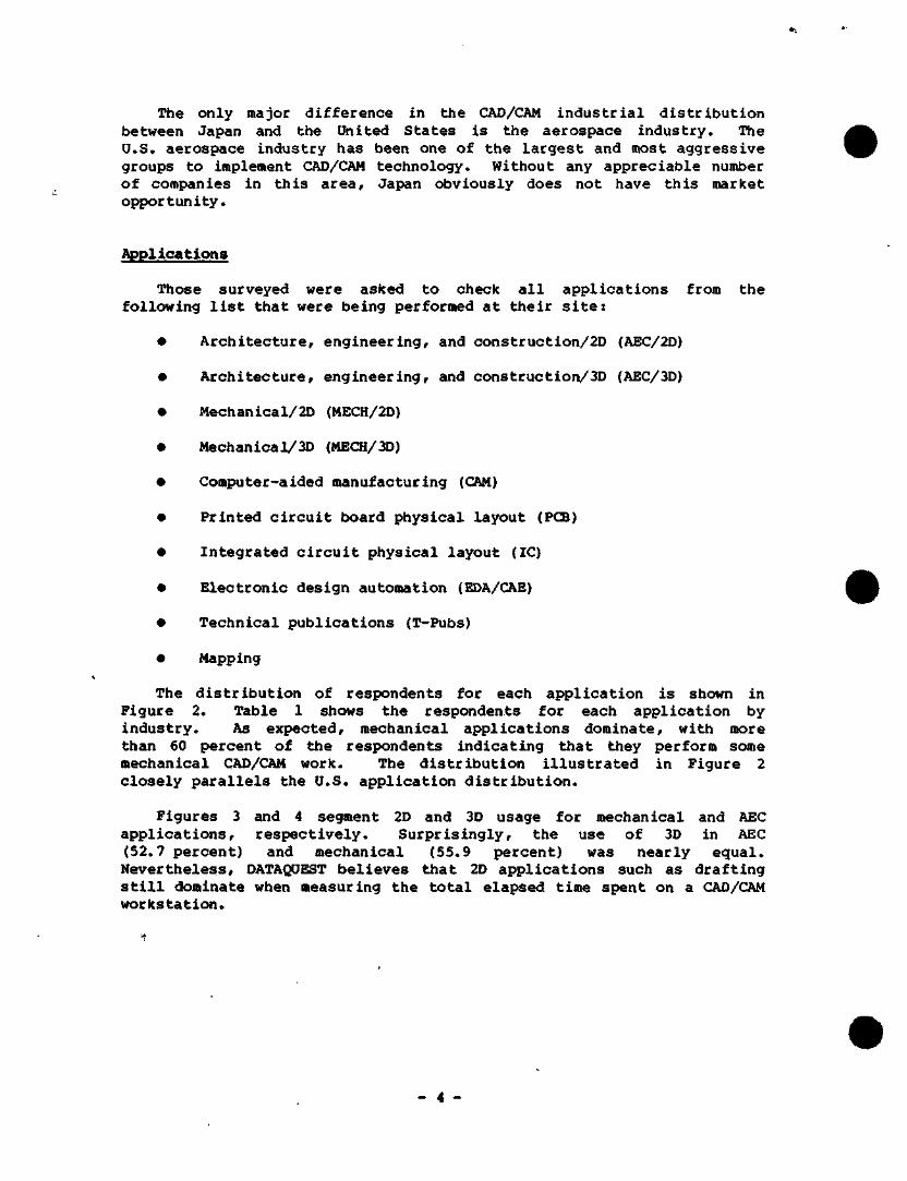
The only major difference in the CAD/CAM industrial distribution between Japan and the United States is the aerospace industry. The U.S. aerospace industry has been one of the largest and most aggressive groups to implement CAD/CAM technology. Without any appreciable number of companies in this area, Japan obviously does not have this market opportunity.
j^plications
Those surveyed were asked to check all applications from the following list that were being performed at their site:
Architecture, engineering, and construction/2D (AEC/2D)
Architecture, engineering, and construction/3D (AEC/3D)
Mechanical/2D (MECH/2D)
Mechanical/3D (MECH/3D)
Computer-aided manufacturing (CAM)
Printed circuit board physical layout (PCS)
Integrated circuit physical layout (IC)
Electronic design automation (EDA/CAE)
Technical publications (T-Pubs)
Mapping
The distribution of respondents for each application is shown in Figure 2. Table 1 shows the respondents for each application by industry. As expected, mechanical applications dominate, with more than 60 percent of the respondents indicating that they perform some mechanical CAD/CAM work. The distribution illustrated in Figure 2 closely parallels the U.S. application distribution.
Figures 3 and 4 segment 2D and 3D usage for mechanical and AEC applications, respectively. Surprisingly, the use of 3D in AEC (52.7 percent) and mechanical (55.9 percent) was nearly equal. Nevertheless, DATAQUEST believes that 2D applications such as drafting still dominate when measuring the total elapsed time spent on a CAO/CAM workstation.
- 4 -
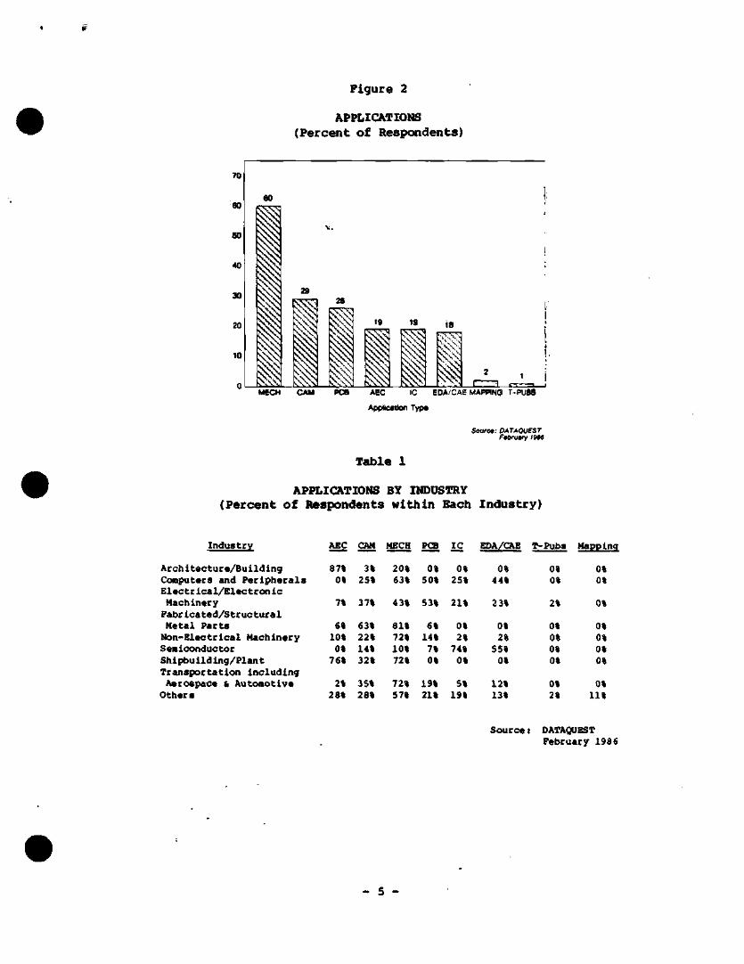
Figure 2
APPLICATIONS (Percent of Respondents)
MtCH CAM PCB AEC IC EDA/CAE MAPPING T-PUSS
AppIicstIon Type
Source: DATAQUEST February 1966
Table 1
APPLICATIONS BY INDUSTRY (Percent of Respondents within Each Industry)
Industry
Architecture/Building Computers and Peripherals Electrical/Electronic Machinery Fabr ica ted/Str uc tura1 Metal Parts
Non-E lectrical Machinery Semiconductor Shipbui lding /P lant Treuisportation inc luding
Aerospace 6 Automotive Others
AEC CAM MECH PCB IC EDA/CAE T-Pubs Mapping
87% 0%
7%
6« 10% 0% 76%
2% 28%
3% 25%
37%
63% 22% 14% 32%
35% 28%
20% 63%
43%
81% 72% 10% 72%
72% 57%
0% 50%
53%
6% 14% 7% 0%
19% 21%
0% 25%
21%
0% 2% 74% 0%
5% 19%
0% 44%
23%
0% 2%
55% 0%
12% 13%
Source:
0% 0%
2%
0% 0% 0% 0%
0% 2%
0% 0%
0«
0% 0% 0% 0%
0% 11%
DATAQUEST February 1986
- 5 -
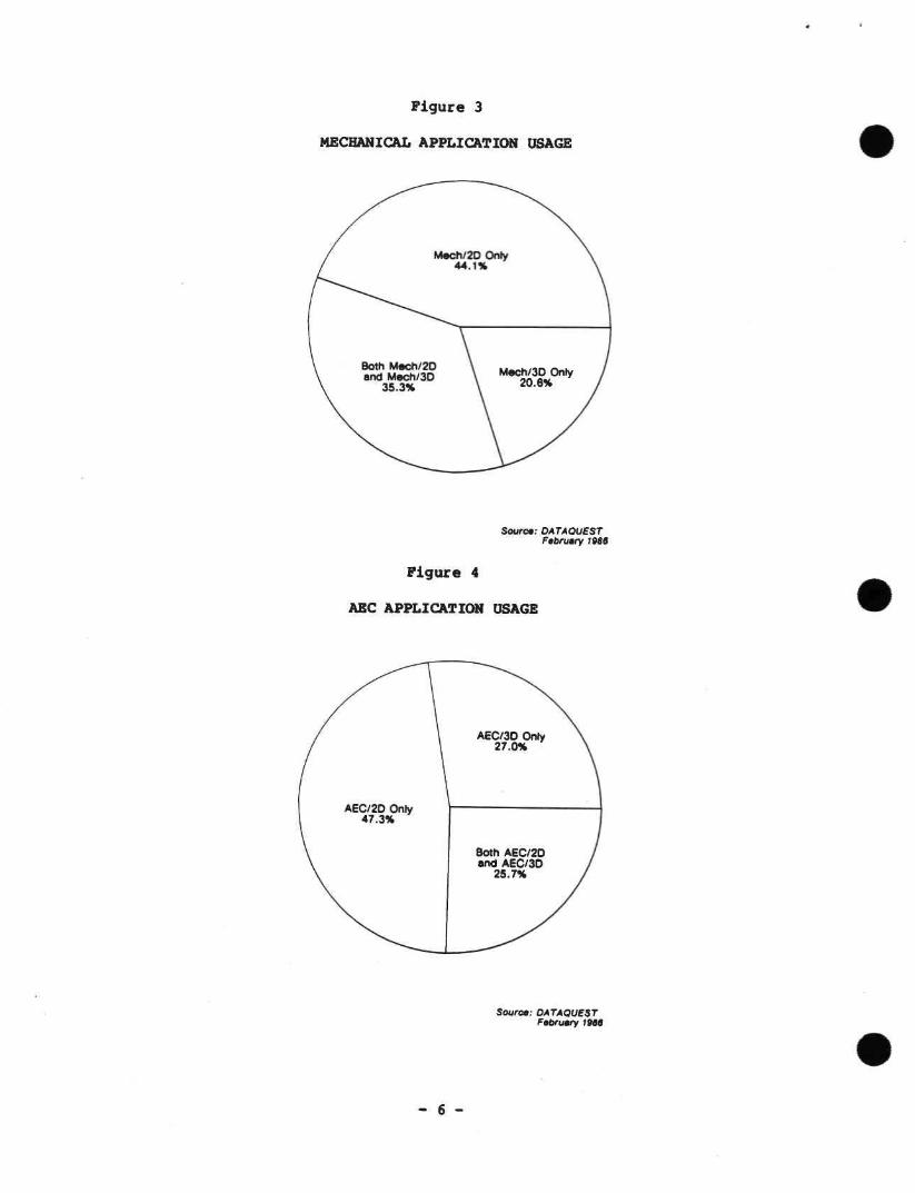
Figure 3
MECHANICAL APPLICATION USAGE
Sourot: DATAOUeST Febniaty 1989
Figure 4
ABC APPLICATION USAGE
Source; DATAOUEST Fabrumy >M0
- 6 -
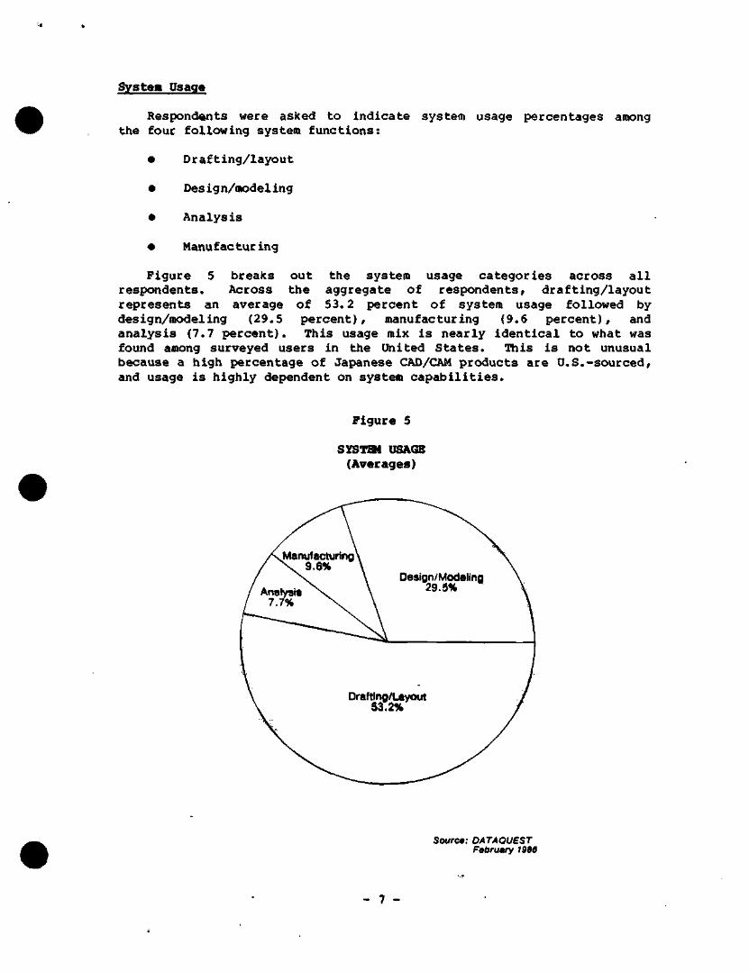
System Usage
Respondants were asked to indicate system usage percentages among the four following system functions:
• Drafting/layout
• Design/modeling
• Analysis
• Manufacturing
Figure 5 breaks out the system usage categories across all respondents. Across the aggregate of respondents, drafting/layout represents an average of 53.2 percent of system usage followed by design/modeling (29.5 percent), manufacturing (9.6 percent), and analysis (7.7 percent). This usage mix is nearly identical to what was found among surveyed users in the United States. This is not unusual because a high percentage of Japanese CAD/CAM products are U.S.-sourced, and usage is highly dependent on system capabilities.
Figure 5
SYSTBf USAGE (Averages)
Source: DATAOUEST February 1986
- 7 -
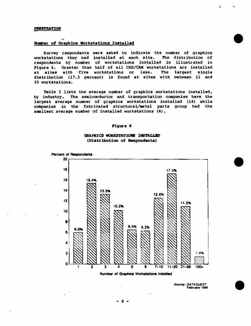
PENETRATION
Nuaber of Graphics Workstations Installed
Survey respondents were asked to indicate the number of graphics worlcstations they had installed at each site. The distribution of respondents by number of workstations installed is illustrated in Figure 6. Greater than half of all CAD/CAM workstations are installed at sites with five workstations or less. The largest single distribution (17.3 percent) is found at sites with between 11 and 20 workstations.
Table 2 lists the average number of graphics workstations installed, by industry. The semiconductor and transportation companies have the largest average number of graphics workstations installed (16) while companies in the fabricated structural/metal parts group had the smallest average number of installed workstations (6).
Figure 6
GRAPHICS WORKSTATIONS INSTALLED (Distribution of Respondents)
Percent of ResIsondents 20
3 4 5 6 7-10 11-20 21-99
Number of Qraphics Workstatkms Installed
Source: DATAOUEST February 1986
- 8 -
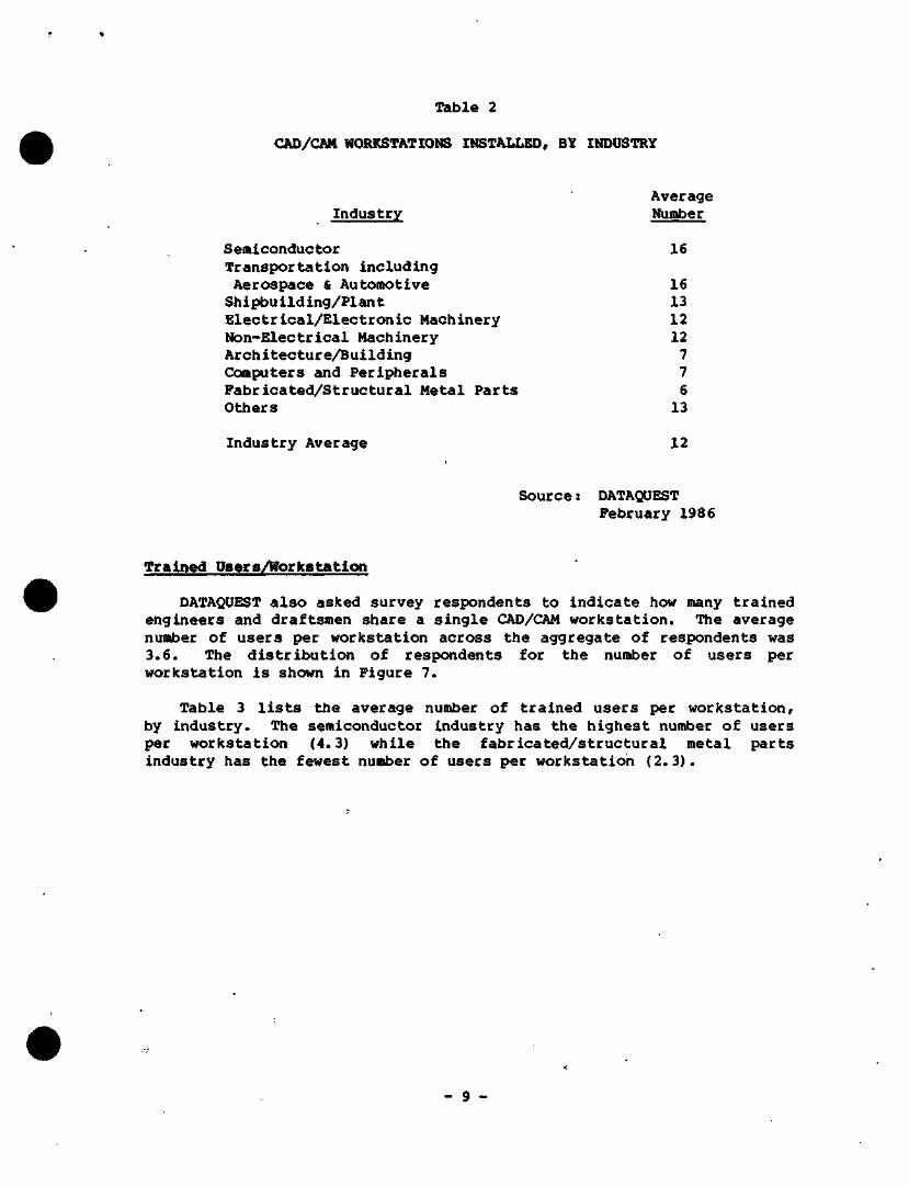
Table 2
CAD/CAN WORKSTATIONS INSTALLED, BY INDUSTRY
Average Industry Number
Semiconductor 16 Transportation including Aerospace & Automotive 16 Shipbuilding/Plant 13 Electrical/Electronic Machinery 12 Non-Electrical Machinery 12 Architecture/Building 7 Computers and Peripherals 7 Fabricated/Structural Metal Parts 6 Ottiers 13
Industry Average 12
Source: DATAQUEST February 1986
Trained Osers/Workatation
DATAQUEST also asked survey respondents to indicate how many trained engineers and draftsmen share a single CAD/CAM workstation. The average number of users per workstation across the aggregate of respondents was 3.6. The distribution of respondents for the number of users per workstation is shown in Figure 7.
Table 3 lists the average nuntber of trained users per workstation, by industry. The semiconductor industry has the highest number of users per workstation (4.3) while the fabricated/structural metal parts industry has the fewest number of users per workstation (2.3).
- 9 -
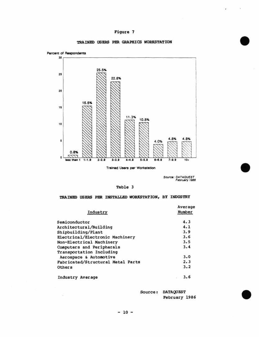
Figure 7
TRAINED USBBS PER GRAPHICS WORKSTATION
Percent of Respondents 30
iMtttian I 1-1.9 2-2.9 3-3.9 4-4.9 5-5.9 6-6.9
Trained Users per Workstation
7-9.9
Source: DATAOUSST February 198S
Table 3
TRAINED USERS PER INSTALLED WORKSTATION, BY INDUSTRY
Industry
Semiconductor Arch i tec tur a 1/fiu ild ing Shipbuilding/Plant Electrical/Electronic Machinery Non-Electrical Machinery Computers and Peripherals Transportation Including Aerospace & Automotive
Fabricated/Structural Metal Parts Others
Industry Average
Average Number
4.3 4.1 3.9 3.6 3.5 3.4
3.0 2.3 3.2
3.6
'Source; DATAQUEST February 1986
- 10 -
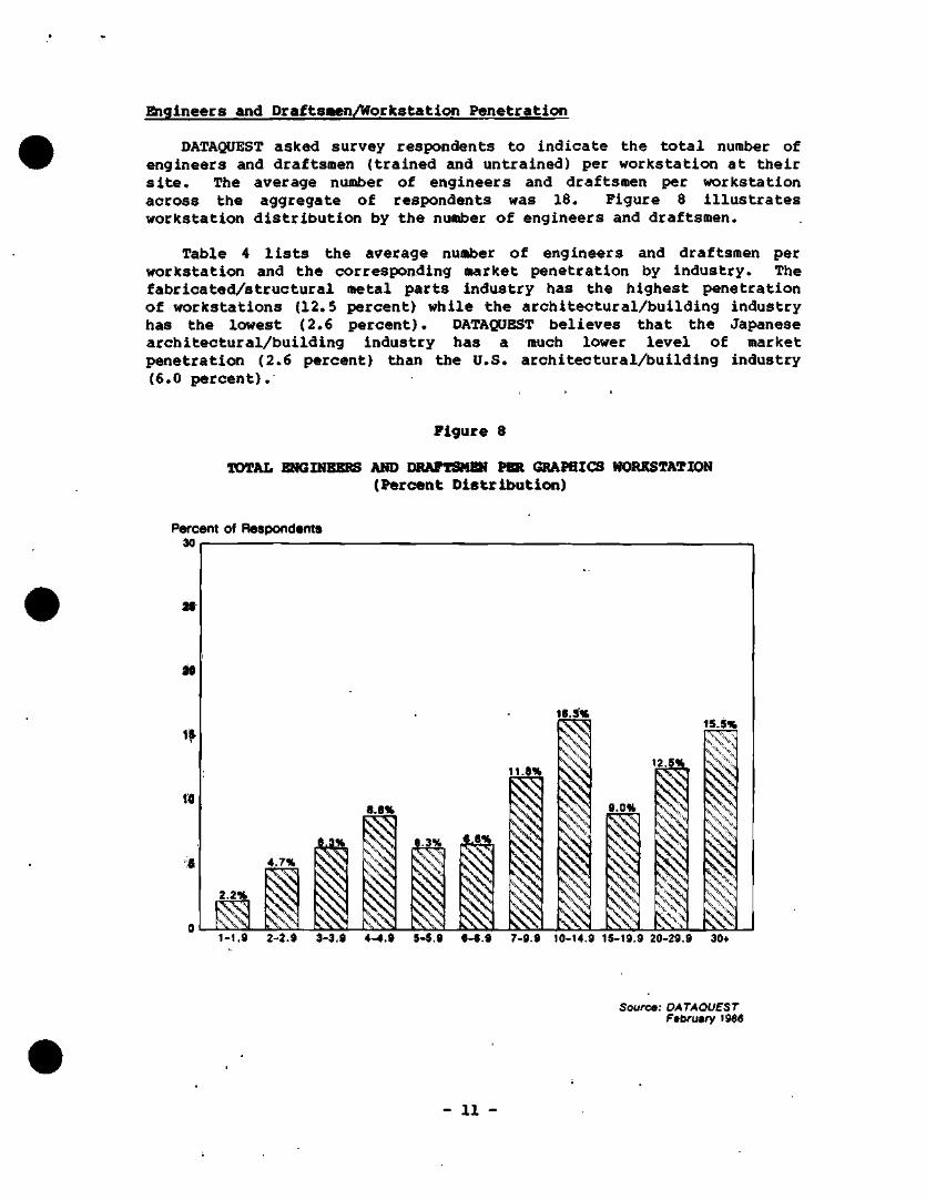
Engineers and Draftsaen/Workstation Penetration
DATAQUEST asked survey respondents to indicate the total number of engineers and draftsmen (trained and untrained) per workstation at their site. The average number of engineers and draftsmen per workstation across the aggregate of respondents was 18. Figure 8 illustrates workstation distribution by the number of engineers and draftsmen.
Table 4 lists the average number of engineers and draftsmen per workstation and the corresponding market penetration by industry. The fabricated/structural metal parts industry has the highest penetration of workstations (12.5 percent) while the architectural/building industry has the lowest (2.6 percent). DATAQUEST believes that the Japanese architectural/building industry has a much lower level of market penetration (2.6 percent) than the U.S. architectural/building industry (6.0 percent).
Figure 8
TOTAL ENGINEERS AND DRAFTSMEN PER GRAPHICS WORKSTATION (Percent Distribution)
Percent of Respondents 30 r-
1-1.9 2-2.9 3-3.9 4-4.9 5-5.9 6-6.9 7-9.9 10-14.9 15-19.9 20-29.9 30+
Source: DATAQUEST February 1986
- 11 -
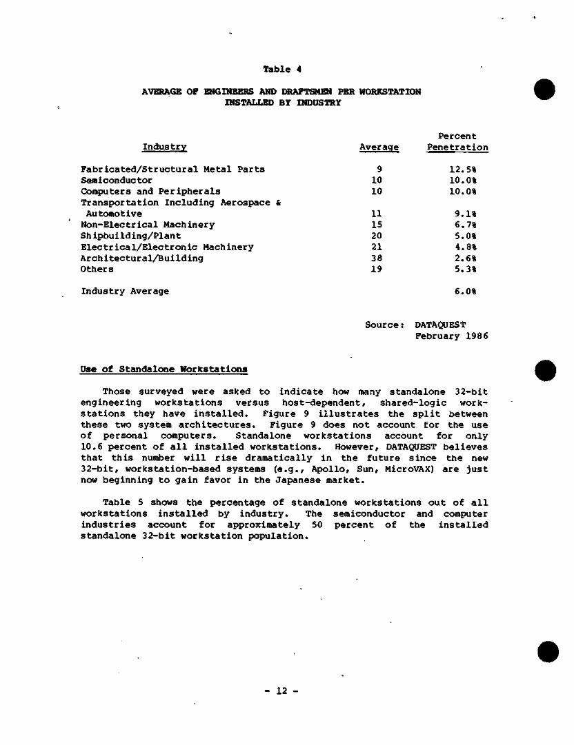
Table 4
AVERAGE OF SIGINEEKS AND DRAFTSMEN PER WORKSTATION INSTALLED BY INDUSTRY
Industry
Fabricated/Structural Metal Parts Semiconductor Computers and Peripherals Transportation Including Aerospace & Automotive Non-Electrical Machinery Shipbuilding/Plant Electrical/Electronic Machinery Architectural/Building Others
Average
9 10 10
11 15 20 21 38 19
Percent Penetration
12.5% 10.0% 10.0%
9.1% 6.7% 5.0% 4.8% 2.6% 5.3%
Industry Average 6.0%
Source I DATAQUEST February 1986
Use of Standalone Workstations
Those surveyed were asked to indicate how many standalone 32-bit engineering workstations versus host-dependent, shared-logic workstations they have installed. Figure 9 illustrates the split between these two system architectures. Figure 9 does not account for the use of personal computers. Standalone workstations account for only 10.6 percent of all installed workstations. However, DATAQUEST believes that this number will rise dramatically in the future since the new 32-bit, workstation-based systems (e.g., Apollo, Sun, MicroVAX) are just now beginning to gain favor in the Japanese market.
Table 5 shows the percentage of standalone workstations out of all workstations installed by industry. The semiconductor and computer industries account for approximately 50 percent of the installed standalone 32-bit workstation population.
- 12 -
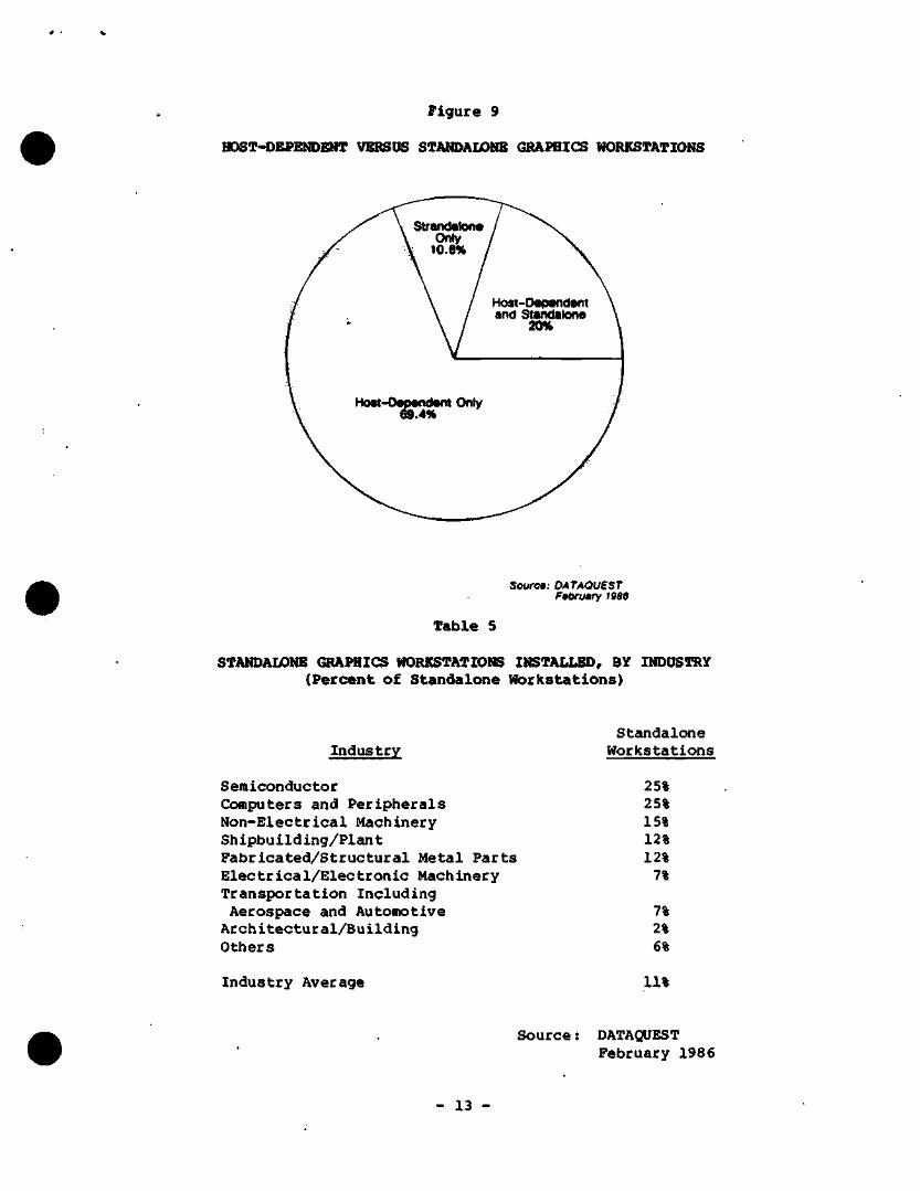
Figure 9
HOST^EPENDENT VERSUS STANDALONE GRAPHICS WORKSTATIONS
Source; DATAOUEST February 1988
Table 5
STANDALONE GRAPHICS WORKSTATIONS INSTALLED, BY INDUSTRY (Percent of Standalone WorIcstations)
Industry
Semiconductor Computers and Peripherals Non-Electrical Machinery Shipbuilding/Plant Fabricated/Structural Metal Parts Electrical/Electronic Machinery Transportation Including Aerospace and Automotive Architectural/Building Others
Standalone Workstations
25% 25% 15% 12% 12% 7%
7% 2% 6%
Industry Average 11%
Source I DATAQUEST February 1986
- 13 -
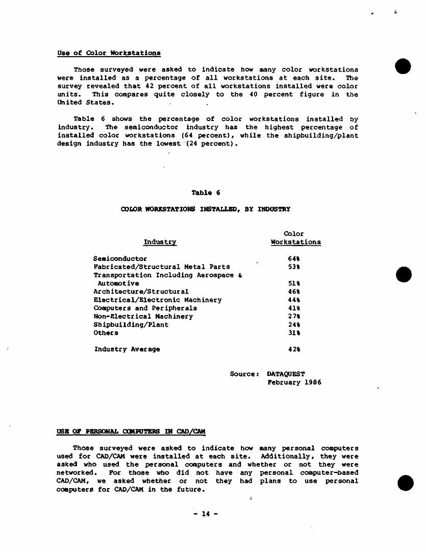
Use of Color Workstatitms
Those surveyed were asked to indicate how many color workstations were installed as a percentage of all workstations at each site. The survey revealed that 42 percent of all workstations installed were color units. This compares quite closely to the 40 percent figure in the United States.
Table 6 shows the percentage of color workstations installed by industry. The semiconductor industry has the highest percentage of installed color workstations (64 percent), while the shipbuilding/plant design industry has the lowest (24 percent).
Table 6
COLOR WORKSTATIONS INSTALLED, BY INDUSTRY
Color Industry Workstations
Semiconductor 64% Fabricated/Structural Metal Parts 53% Transportation Including Aerospace & Automotive 51% Architecture/Structural 46% Electrical/Electronic Machinery 44% Computers and Peripherals 41% Non-Electrical Machinery 27% Shipbuilding/Plant 24% Others 31%
Industry Average 42%
Source: DATAQUEST February 1986
DSB (MP PERSONAL OOMHITERS IN CAD/CftM
Those surveyed were asked to indicate how many personal computers used for CAD/CAM were installed at each site. Additionally, they were asked who used the personal computers and whether or not they were networked. For those who did not have any personal computer-based CAD/CAM, we asked whether or not they had plans to use personal computers for CAD/CAM in the future.
- 14 -
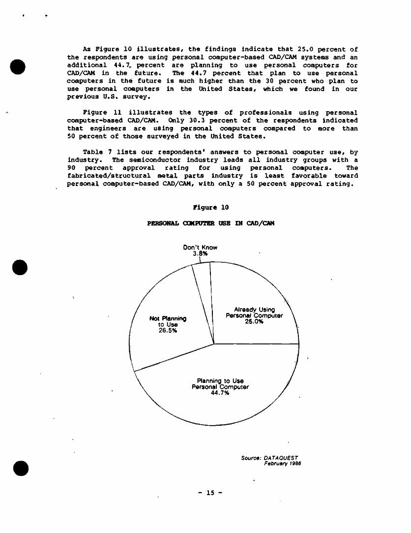
As Figure 10 illustrates, the findings indicate that 25.0 percent of the respondents are using personal computer-based CAD/CAM systems and an additional 44.7^ percent are planning to use personal computers for CAD/CAM in the future. The 44.7 percent that plan to use personal computers in the future is much higher than the 30 percent who plan to use personal computers in the United States, which we found in our previous U.S. survey.
Figure 11 illustrates the types of professionals using personal computer-based CAD/CAM. Only 30.3 percent of the respondents indicated that engineers are using personal computers compared to more than 50 percent of those surveyed in the United States.
Table 7 lists our respondents' answers to personal computer use, by industry. The semiconductor industry leads all industry groups with a 90 percent approval rating for using personal computers. The fabricated/structural metal parts industry is least favorable toward personal computer-based CAD/CAM, with only a 50 percent approval rating.
Figure 10
PERSONAL OQMFUTBR USE IN CAD/CAM
Don't Know 3,8%
Source: DATAOUEST February 1986
- 15 -
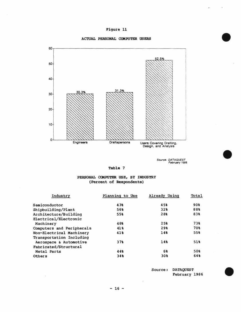
Figure 11
ACTUAL PERSCOIAL COMPUTER USERS
Englneera Oraftsparsons Users Covering Oraftino, Design, and Analysis
Source: DATAQUEST February 198S
Table 7
PERSONAL COMPUTER USE, BY INDUSTRY (Percent of Respondents)
Industry
Semiconductor Shipbu i ld ing/P lan t Archi tec ture /Bu i ld ing E l e c t r i c a l / E l e c t r o n i c Machinery
Computers and P e r i p h e r a l s Non -E lec t r i ca l Machinery T ranspo r tat ion Including
Aerospace & Autc^notive Fab r i ca ted /St ructu ra l Metal Pa r t s
Others
P lann ing t o Use
43% 56% 55%
48% 41% 41%
37%
44% 34%
Already Using
45% 32% 28%
25% 29% 14%
14%
6% 30%
Itotal
90% 88% 83%
73% 70% 55%
51%
50% 64%
Sou rce; DATAQUEST February 1986
- 16 -
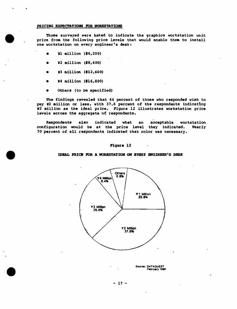
PRICING EXHBCTATIONS FOR WORKSTATIONS
Those surveyed were dsked to indicate the graphics workstation unit price from the following price levels that would enable them to install one workstation on every engineer's desk:
¥1 million ($4,200)
V2 million ($8,400)
V3 million ($12,600)
V4 million ($16,800)
Others (to be specified)
The findings revealed that 64 percent of those who responded wish to pay y2 million or less, with 37.6 percent of the respondents indicating V2 million as the ideal price. Figure 12 illustrates workstation price levels across the aggregate of respondents.
Respondents also indicated what an acceptable workstation configuration would be at the price level they indicated. Nearly 70 percent of all respondents indicated that color was necessary.
Figure 12
IDEAL PRICE FOR A WORKSTATION ON EVERY ENGINEER'S DESK
Source; DATAOUEST February 1986
- 17 -
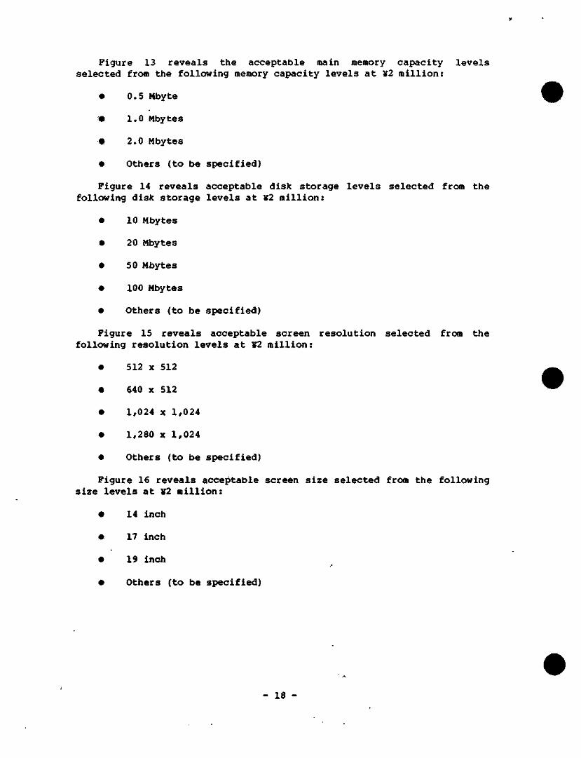
Figure 13 reveals the acceptable main memory capacity levels selected from the following memory capacity levels at ¥2 million:
• 0.5 Mbyte
• 1.0 Mbytes
• 2.0 Mbytes
• Others (to be specified)
Figure 14 reveals acceptable disk storage levels selected from the following disk storage levels at V2 million:
• 10 Mbytes
• 20 Mbytes
• 50 Mbytes
• 100 Mbytes
• Others (to be specified)
Figure 15 reveals acceptable screen resolution selected from the following resolution levels at V2 million:
• 512 X 512
• 640 X 512
• 1,024 X 1,024
• 1,280 X 1,024
• Others (to be specified)
Figure 16 reveals acceptable screen size selected from the following size levels at V2 million:
• 14 inch
• 17 inch
• 19 inch
• Others (to be specified)
- 18 -
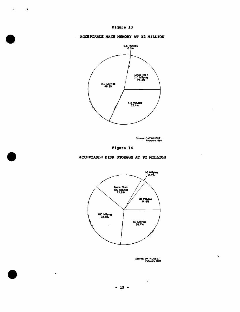
F i g u r e 13
ACCEPTABLE MAIM MSIORY AT V2 MILLION
0.5 MBytes 0.0%
Source: DATAQUEST February >M«
Figure 14
ACCEPTABLE DISK STORAGE AT V2 MILLION
to MBytM 2 .1%
Sourca: DATAQUEST February 1989
- 19 -
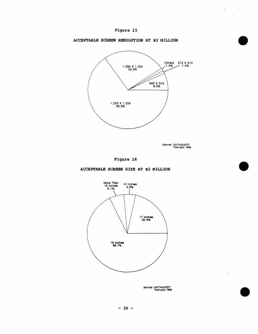
Figure 15
ACCEPTABLE SCREEN RESOLUTION AT V2 MILLION
Others 5 1 2 X 5 1 2 1.4%
Source: DATAOUEST February I98t
Figure 16
ACCEPTABLE SCREEN SIZE AT V2 MILLION
Mors Than 19 Inches
6 .1%
14 Inches 4.a%
Source: OATAQUEST February 1988
- 20 -
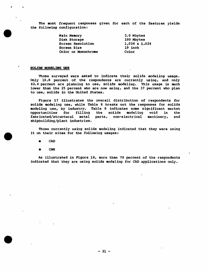
The most frequent responses given for each of the features yields the following configuration:
Main Memory 2.0 Mbytes DisI( Storage 100 Mbytes Screen Resolution 1,024 x 1,024 Screen Size 19 inch Color or Monochrome Color
SOLIDS MODELING USE
Those surveyed were asked to indicate their solids modeling usage. Only 10.8 percent of the respondents are currently using, and only 42.4 percent are planning to use, solids modeling. This usage is much lower than the 25 percent who are now using, and the 37 percent who plan to use, solids in the United States.
Figure 17 illustrates the overall distribution of respondents for solids modeling use, while Table 8 breaks out the responses for solids modeling use, by industry. Table 8 indicates some significant market opportunities for filling the solids modeling void in the fabricated/structural metal parts, non-electrical machinery, and shipbuilding/plant industries.
Those currently using solids modeling indicated that they were using it on their sites for the following usages:
• CAD
• CAM
As illustrated in Figure 18, more than 70 percent of the respondents indicated that they are using solids modeling for CAD applications only.
- 21 -
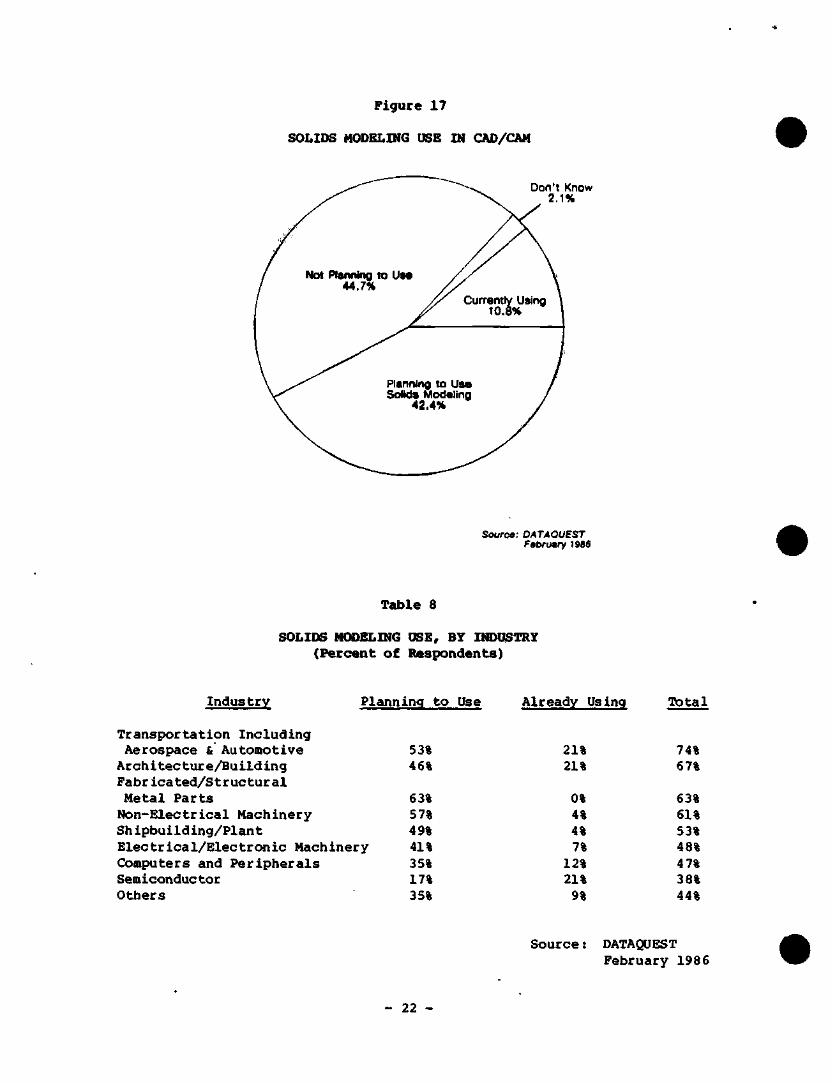
Figure 17
SOLIDS MODELING USB IN CAD/CAM
Don't Know 2.1%
Source: DATAQUEST February 1986
Table 8
SOLIDS MODELING OSE, BY INDIISTRY (Percent of Respondents)
Industry Planning to Use
Transportation Including Aerospace & Automotive 53% Architecture/Building 46% Fabricated/Structural Metal Parts 63% Non-Electrical Mactiinery 57% Shipbuilding/Plant 49% Electrical/Electronic Machinery 41% Computers and Peripherals 35% Semiconductor 17% Others 35%
Already Using Total
21% 74% 21% 67%
0% 63% 4% 61% 4% 53% 7% 48%
12% 47% 21% 38% 9% 44%
Source: DATAQUEST February 1986
- 22 -
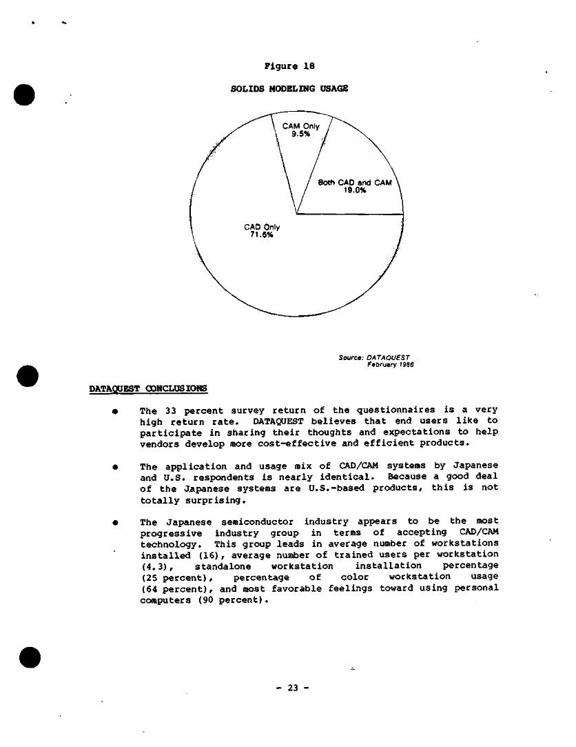
Figure 18
SOLIDS MODELING USAGE
Source; DATAOUEST February 7986
DATAQOEST OONCLUSIONS
• The 33 percent survey return of the questionnaires is a very high return rate. DATAQUEST believes that end users like to participate in sharing their thoughts and expectations to help vendors develop more cost-effective and efficient products.
• The application and usage mix of CAD/CAM systems by Japanese and U.S. respondents is nearly identical. Because a good deal Of the Japanese systems are U.S.-based products, this is not totally surprising.
• The Japanese semiconductor industry appears to be the most progressive industry group in terms of accepting CAD/CAM technology. This group leads in average number of worlcstations installed (16), average number of trained users per workstation (4.3), standalone workstation installation percentage (25 percent), percentage of color workstation usage (64 percent), and most favorable feelings toward using personal computers (90 percent).
- 23 -
• standalone workstations and personal computers are beginning to play an important role in Japan. Although respondents indicated that standalone and personal computer usage was quite low, DATAQUEST believes that these two architectures will soon dominate new CAD/CAM systems shipments.
• Overall Japanese market penetration (6 percent) is still very low. DATAQUEST expects that the Japanese market will grow at or above that of the United States over the next five years.
(This newsletter is reprinted with the permission of DATAQUEST's CAD/CAM Industry Service.)
Sheridan Tatsuno Yu Uemura
- 24 -
Dataquest JAPANESE RESEARCH NEWSLETTER
JSIS Code: Newsletters 1985-1986, JSIA 1986-11
JAPANESE SmZCONDUCTOR TECHNOLOGY TRENDS FOURTH QUARTER 1985
SUMMARY
"From copycats-in-kimono to innovators-in-bunny suits." If there is one major theme underlying Japanese technology trends, DATAQUEST believes that it is Japan's growing determination to become more innovative in electronics. During the last quarter of 1985, we observed several developments that suggest Japan is rapidly becoming a technological powerhouse. These events include:
The establishment of electronics (1984-1988)
76 basic research laboratories in
The opening of electronics R&D labs by Japanese automobile makers such as Honda and Nissan
Growing interest in Japanese technology by the United States and Soviet Union
The competitiveness of Japanese supercomputers and their growing use in VLSI design
The commercialization of automated language translators (the goal of MITI's fifth-generation computer project) for information gathering, factory automation, and eventually telephone systems
The establishment of new national R&D projects in laser applications, synchrotron radiation, automated telephone translators, intersatellite laser communications, and explosive pulse electricity
Joint development of VLSI technology by Nippon Telegraph and Telephone (NTT), Motorola, and Texas Instruments
1986 Dataquest Incorporated Feb. 14 ed.-Reproduction Prohibited
The content ot this report represents our interpretaion and analysis of information generally available lo the public or released by responsible individuals in the subject companies, but is not guaranteed as to accuracy or compleleness. It does not contain material provided to us in confidence by our clients Individual companies reported on and analyzed by DATAQUEST, may be clients of ttiis and/or other DATAQUEST services This information is not furnished in connection with a sale or offer to sell securities or in connection with the solicitation of an offer to buy securities This firm and its parent and/or their officers, stockholders, or members of their families may, from time to time, have a long or short rtncitinn in thA <tAriiritit4R mentioned and mav sell or buv such securities
Azabu Heights, Suite 711, 1-5-10 Roppongi, Minato-ku, Tokyo 106, Japan 1290 Rldder Park Drive / San Jose, CA 95131 / (408) 971-9000 / Telex 171973
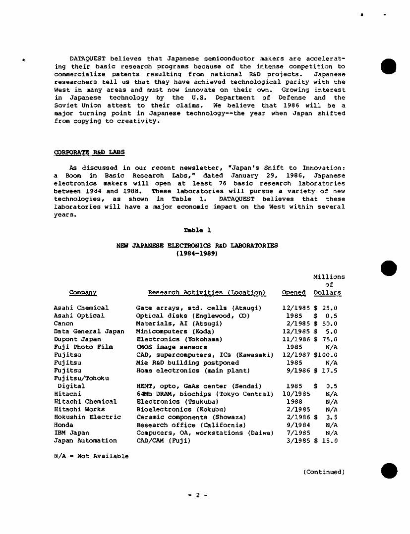
DATAQUEST believes that Japanese semiconductor makers are accelerating their basic research programs because of the intense competition to commercialize patents resulting from national R&D projects. Japanese researchers tell us that they have achieved technological parity with the West in many areas and must now innovate on their own. Growing interest in Japanese technology by the U.S. Department of Defense and the Soviet Union attest to their claims. We believe that 1986 will be a major turning point in Japanese technology—the year when Japan shifted from copying to creativity.
CORPORATE R&D LABS
As discussed in our recent newsletter, "Japan's Shift to Innovation: a Boom in Basic Research Labs," dated January 29, 1986, Japanese electronics makers will open at least 76 basic research laboratories between 1984 and 1988. These laboratories will pursue a variety of new technologies, as shown in Table 1. DATAQUEST believes that these laboratories will have a major economic impact on the West within several years.
Table 1
NEW JAPANESE ELECTRONICS R&O LABORATORIES (1984-1989)
Company
Asahi Chemical Asahi Optical Canon Data General Japan Dupont Japan Fuji Photo Film Fujitsu Fujitsu Fujitsu Fuj itsu/Tohoku Digital Hitachi Hitachi Chemical Hitachi Works Hokushin Electric Honda IBM Japan Japan Automation
Research Activities (Location)
Gate arrays, std. cells (Atsugi) Optical disks (Englewood, CO) Materials, AI (Atsugi) Minicomputers (Koda) Electronics (Yokohama) CMOS image sensors CAD, supercomputers, ICs (Kawasaki) Mie R&D building postponed Home electronics (main plant)
HEMT, opto, GaAs center (Sendai) 64Mb DRAM, biochips (Tokyo Central) Electronics (TSukuba) Bioelectronics (Kokubu) Ceramic components (Showaza) Research office (California) Computers, OA, workstations (Daiwa) CAD/CAM (Fuji)
Mi .llions of
Opened Dollars
12/1985 $ 1985 $ 2/1985 $ 12/1985 $ 11/1986 $ 1985
25.0 0.5 50.0 5.0 75.0 N/A
12/1987 $100.0 1985 9/1986 $
1985 $ 10/1985 1988 2/1985 2/1986 $ 9/1984 7/1985
N/A 17.5
0.5 N/A N/A N/A 3.5 N/A N/A
3/1985 $ 15.0
N/A = Not Available
(Continued)
- 2 -
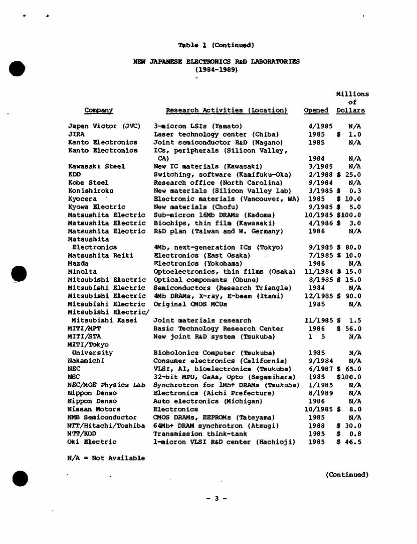
Table 1 (Continued)
NEW JAPANESE ELECTRONICS R&D LABORATORIES (1984-.1989)
Company
Japan Victor (JVC) JIRA Kanto Electronics Kanto Electronics
Kawasaki Steel KDD Kobe Steel Konishiroku Kyocera Kyowa Electric Matsushita Electric Matsushita Electric Matsushita Electric Matsushita Electronics
Matsushita Reiki Mazda Minolta Mitsubishi Electric Mitsubishi Electric Mitsubishi Electric Mitsubishi Electric Mitsubishi Electric/ Mitsubishi Kasei MITI/MPT MITI/STA MITI/Tokyo University Nakamichi NEC NEC NEC/MOE Physics Lab Nippon Denso Nippon Oenso Nissan Motors NMB Semiconductor NTT/Hitachi/TOshiba NTT ADD Oki Electric
N/A = NOt Available
Research Activities (Location)
3-micron LSIs (Yamato) Laser technology center (Chiba) Joint semiconductor R&D (Nagano) ICs, peripherals (Silicon Valley, CA) New IC materials (Kawasaki) Switching, software (Kamifuku-Oka) Research office (North Carolina) New materials (Silicon Valley lab) Electronic materials (Vancouver, WA) New materials (Chofu) Sub-micron 16Mb DRAMs (Kadoma) Biochips, thin film (Kawasaki) R&D plan (Taiwan and W. Germany)
4Mb, next-generation ICs (Tokyo) Electronics (East Osaka) Electronics (Yokohama) Optoelectronics, thin films (Osaka) Optical components (Obune) Semiconductors (Research Triangle) 4Mb DRAMs, X-ray, E-beam (Itami) Original CMOS MCUs
Joint materials research Basic Technology Research Center New joint R&D system (TSukuba)
Bioholonics Computer (Tsukuba) Consumer electronics (California) VLSI, AI, bioelectronics (Tsukuba) 32-bit MPU, GaAs, Opto (Sagamihara) Synchrotron for lMb+ DRAMs (TSukuba) Electronics (Aichi Prefecture) Auto electronics (Michigan) Electronics CMOS DRAMs, EEPRQMs (Tateyama) 64Mb+ DRAM synchrotron (Atsugi) Transmission think-tank 1-micron VLSI R&D center (Hachioji)
Millions Of
Opened Dollars
4/1985 1985 $ 1985
1984 3/1985 2/1988 $ 9/1984 3/1985 $ 1985 $ 9/1985 $
N/A 1.0 N/A
N/A N/A 25.0 N/A 0.3 10.0 5.0
10/1985 $100.0 4/1986 $ 1986
9/1985 $ 7/1985 $ 1986 11/1984 $
3.0 N/A
80.0 10.0 N/A 15.0
8/1985 $ 15.0 1984 N/A 12/1985 $ 90.0 1985 N/A
11/1985 $ 1986 3 1 5
1985 9/1984 6/1987 $
1.5 56.0 N/A
N/A N/A 65.0
1985 $100.0 1/1985 8/1989 1986 10/1985 $ 1985 1988 $ 1985 $ 1985 $
N/A N/A N/A 8.0 N/A 30.0 0.8
46.5
(Continued)
- 3 -
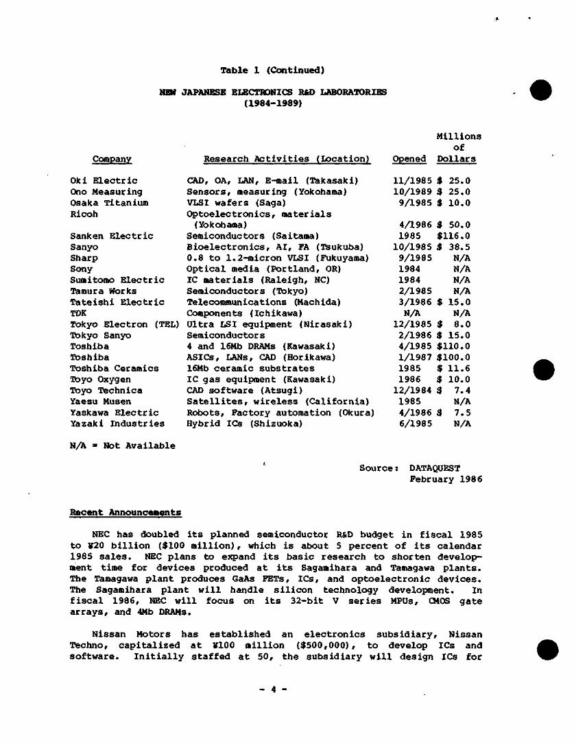
Table 1 (Continued)
NEW JAPANESE ELECTRONICS R«D LABORATORIES (1984-1989)
Company
Oki Electric Ono Measuring Osaka Titanium Ricoh
Sanken Electric Sanyo Sharp Sony Sumitomo Electric Tamura Works Tateishi Electric TDK Tokyo E lec t ron (TEL) Tokyo Sanyo Toshiba Tostiiba Toshiba Ceramics Toyo Oxygen Toyo Technica Yaesu Musen Yaskawa Electric Yazaki Industries
N/A = Not Available
Research Activities (Location)
CAD, OA, LAN, E-mail (Takasaki) Sensors, measuring (Yokohama) VLSI wafers (Saga) Optoelectronics, materials (Yokohama)
Semiconductors (Saitama) Bioelectronics, AI, FA (Tsukuba) 0.8 to 1.2-micron VLSI (Fukuyama) Optical media (Portland, OR) IC materials (Raleigh, NC) Semiconductors (Tokyo) Telecommunications (Machida) Components (Ichikawa) Ultra LSI equipment (Nirasaki) Semiconductor s 4 and 16Mb DRAMs (Kawasaki) ASICs, LANs, CAD (Horikawa) 16Mb ceramic substrates IC gas equipment (Kawasaki) CAD software (Atsugi) Satellites, wireless (California) Robots, Factory automation (Okura) Hybrid ICs (Shizuoka)
Millions Of
Opened Dollars
11/1985 $ 10/1989 $ 9/1985 $
4/1986 $
25.0 25.0 10.0
50.0 1985 $116.0 10/1985 $ 9/1985 1984 1984 2/1985 3/1986 $ N/A
12/1985 $ 2/1986 $
38.5 N/A N/A N/A N/A 15.0 N/A 8.0 15.0
4/1985 $110.0 1/1987 $100.0 1985 $ 1986 $ 12/1984 $ 1985 4/1986 $ 6/1985
11.6 10.0 7.4 N/A 7.5 N/A
Source: DATAQUEST February 1986
Recent Announcements
NEC has doubled its planned semiconductor R&D budget in fiscal 1985 to ¥20 billion ($100 million), which is about 5 percent of its calendar 1985 sales. NEC plans to expand its basic research to shorten development time for devices produced at its Sagamihara and Tamagawa plants. The Tamagawa plant produces GaAs FETs, ICs, and optoelectronic devices. The Sagamihara plant will handle silicon technology development. In fiscal 1986, NEC will focus on its 32-bit V series MPUs, CMOS gate arrays, and 4Mb DRAMs.
Nissan Motors has established an electronics subsidiary, Nissan Techno, capitalized at VlOO million ($500,000), to develop ICs and software. Initially staffed at 50, the subsidiary will design ICs for
- 4 -
car electronics in 1987. Currently, Nissan buys ICs from Hitachi and NEC, but plans to build its own manufacturing plant within a few years. Other major car makers now in electronics include Toyota, which will build an IC plant by 1988, and GM, which recently bought Electronic Data Systems and Hughes Aircraft. DATAQUEST expects other Japanese car makers to follow suit.
Tokyo Electron (TEL) plans to spend ¥8 billion ($40 million) for plant and equipment in fiscal 1986 (ending September 1986). About $20 million will be spent on semiconductor R&D projects at TEL's new central research institute to be built in Nirasaki, Yamanashi prefecture.
TBCHHOIOGY TRANSFERS
Japanese technologies are being sought increasingly by foreign companies and governments. In December, the Soviet Union's Gosplan (State Planning Committee) presented a list of Japanese technologies that it believes can be obtained under the eased COGQM (Coordinating Coimnittee for Export Control) guidelines. Gosplan's goal is to hold a Japanese industrial fair in Moscow in November 1986. As shown in Table 2, the U.S. Department of Defense submitted a similar list in September 1984. Semiconductors ranked relatively high in both lists. DATAQUEST believes that these lists suggest the relative strength of Japanese technologies.
- 5 -
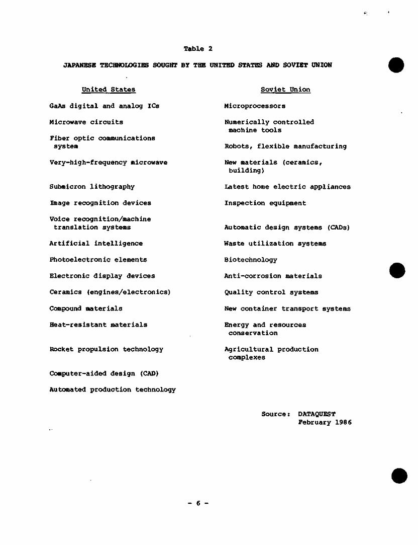
Table 2
JAPANESE TECHNOLOGIES SOUGHT BY THE UNITED STATES AND SOVIET UNION
United States
GaAs digital and analog ICs
Microwave circuits
Fiber optic communications system
Very-high-frequency microwave
Submicron litJiography
Image recognition devices
Voice recognition/machine translation systems
Artificial intelligence
Photoelectronic elements
Electronic display devices
Ceramics (engines/electronics)
Compound materials
Heat-resistant materials
Rocket propulsion technology
Computer-aided design (CAD)
Automated production technology
Soviet Union
Microprocessors
Numerically controlled machine tools
Robots, flexible manufacturing
New materials (ceramics, building)
Latest home electric appliances
Inspection equipnent
Automatic design systems (CADs)
Waste utilization systems
B iotechnology
Anti-corrosion materials
Quality control systems
New container transport systems
Energy and resources conservation
Agricultural production complexes
Source: DATAQUEST February 1986
- 6 -
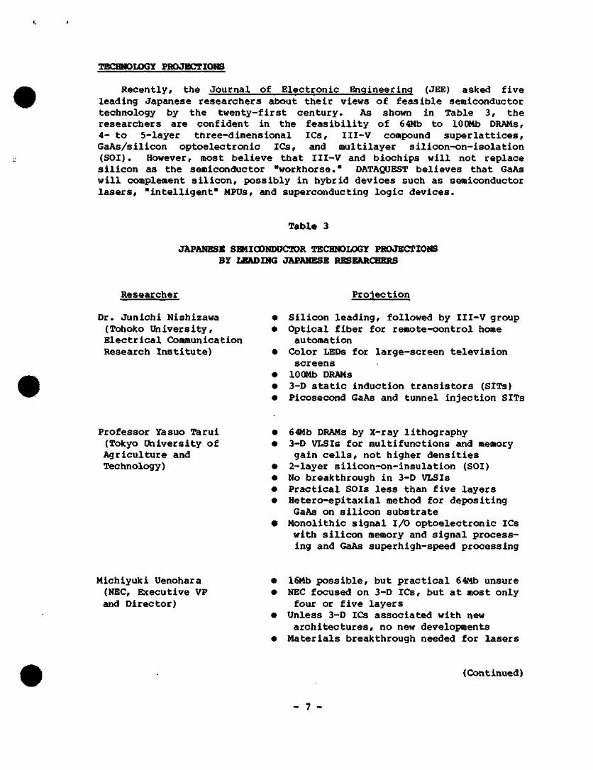
TBCHMOIiOGY PROJBCTIOMS
Recently, the Journal of Electronic Engineering (JEE) asked five leading Japanese researchers about their views of feasible semiconductor technology by the twenty-first century. As shown in Table 3, the researchers are confident in the feasibility of 64Mb to 100Mb DRAMs, 4- to 5-layer three-dimensional ICs, III-V compound superlattices, GaAs/silicon optoelectronic ICs, and multilayer silicon-on-isolation (SOI). However, most believe that III-V and biochips will not replace silicon as the semiconductor "workhorse." DATAQUEST believes that GaAs will complement silicon, possibly in hybrid devices such as semiconductor lasers, "intelligent" MPUs, and superconducting logic devices.
Table 3
JAPANESE SEMICONDUCTOR TECHNOLOGY PROJECTIONS BY LEADING JAPANESE RESEARCHERS
Researcher Projection
Dr. Junichi Nishizawa (Tohoko University, Electrical Communication Research Institute)
Silicon leading, followed by III-V group Optical fiber for remote-control home automation Color LEDs for large-screen television screens 100Mb DRAMs 3-D static induction transistors (SITs) Picosecond GaAs and tunnel injection SITs
Professor Yasuo Tarui (Tokyo University of Agriculture and Technology)
64Mb DRAMs by X-ray lithography 3-D VLSIs for multifunctions and memory gain cells, not higher densities 2-layer silicon-on-insulation (SOI) No breakthrough in 3-D VLSIs Practical SOIs less than five layers Hetero-epitaxial method for depositing GaAs on silicon substrate Monolithic signal I/O optoelectronic ICs with silicon memory and signal processing and GaAs superbigh-speed processing
Michiyuki Uenohara (NEC, Executive VP and Director)
• 16Mb possible, but practical 64Mb unsure • NEC focused on 3-D ICs, but at most only
four or five layers • Unless 3-D ICs associated with new
architectures, no new developments • Materials breakthrough needed for lasers
(Continued)
- 7 -
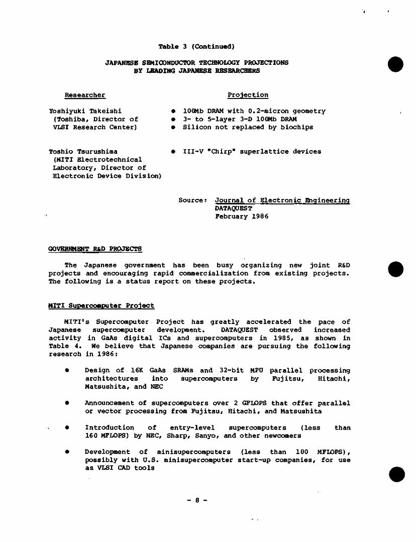
Table 3 (Ccmtinued)
JAPANESE SQ<ICX)NDUCTOR TECHNOLOGY PROJECTIONS BY LEADING JAPANESE RESEARCHERS
Researcher
Yoshiyuki Takeishi (Toshiba, Director of VLSI Research Center)
Projection
• lOQMb DRAM with 0.2-micron geometry • 3- to 5-layer 3-D 100Mb DRAM • Silicon not replaced by biochips
Toshio Tsurushima (MITI Electrotechnical Laboratory, Director of Electronic Device Division)
III-V "Chirp" superlattice devices
Source: Journal of Electronic Engineering DATAQUEST February 1986
GOVERNMENT R&D PROJECTS
The Japanese government has been busy organizing new joint R&D projects and encouraging rapid commercialization from existing projects. The following is a status report on these projects.
MITI Supercomputer Project
MITI's Supercomputer Project has greatly accelerated the pace of Japanese supercomputer development. DATAQUEST observed increased activity in GaAs digital ICs and supercomputers in 1985, as shown in Table 4. We believe that Japanese companies are pursuing the following research in 1986:
• Design of 16K GaAs SRAMs and 32-bit MPU parallel processing architectures into supercomputers by Fujitsu, Hitachi, Matsushita, and NEC
• Announcement of supercomputers over 2 GFLOPS that offer parallel or vector processing from Fujitsu, Hitachi, and Matsushita
Introduction of entry-level supercomputers (less 160 MFLOPS) by NEC, Sharp, Sanyo, and other newcomers
than
Development of minisupercomputers (less than 100 MFLOPS), possibly with U.S. minlsupercomputer start-up companies, for use as VLSI CAD tools
- 8 -
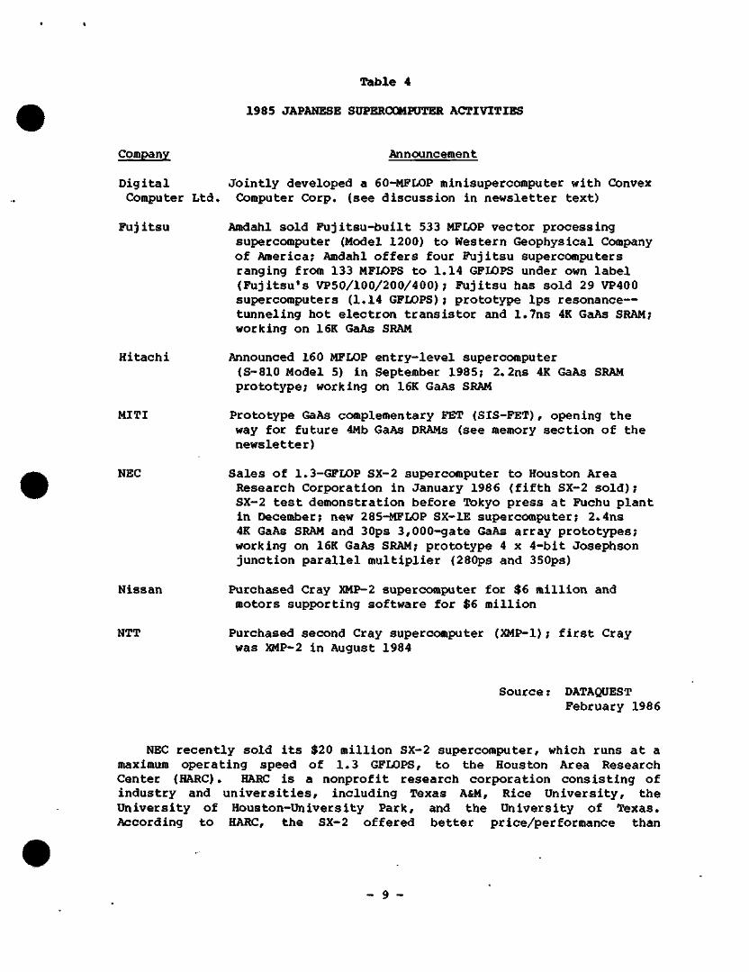
Table 4
1985 JAPANESE SUPERCOMPUTER ACTIVITIES
Company
Digital Computer Ltd,
Fuj itsu
Hitachi
MITI
NEC
Nissan
NTT
Announcement
Jointly developed a 60-MPLOP minisupercomputer with Convex Computer Corp. (see discussion in newsletter text)
Amdahl sold Fujitsu-built 533 MFLOP vector processing supercomputer (Model 1200) to Western Geophysical Company of America; Amdahl offers four Fujitsu supercomputers ranging from 133 MFLOPS to 1.14 GFLOPS under own label (Fujitsu's VP50/100/200/400); Fujitsu has sold 29 VP400 supercomputers (1.14 GFLOPS); prototype Ips resonance— tunneling hot electron transistor and 1.7ns 4K GaAs SRAM; working on 16K GaAs SRAM
Announced 160 MFLOP entry-level supercomputer (S-810 Model 5) in September 1985; 2.2ns 4K GaAs SRAM prototype; working on 16K GaAs SRAM
Prototype GaAs complementary FET (SIS-FET), opening the way for future 4Mb GaAs DRAMs (see memory section of the newsletter)
Sales of 1.3-GFLOP SX-2 supercomputer to Houston Area Research Corporation in January 1986 (fifth SX-2 sold); SX-2 test demonstration before Tokyo press at Fuchu plant in December; n^w 285-MFLOP SX-IE supercomputer; 2.4ns 4K GaAs SRAM and 30ps 3,000-gate GaAs array prototypes; working on 16K GaAs SRAM; prototype 4 x 4-bit Josephson junction parallel multiplier (280ps and 350ps)
Purchased Cray XMP-2 supercomputer for $6 million and motors supporting software for $6 million
Purchased second Cray supercomputer (XMP-1); first Cray was XMP-2 in August 1984
Source: DATAQUEST February 1986
NEC recently sold its $20 million SX-2 supercomputer, which runs at a maximum operating speed of 1.3 GFLOPS, to the Houston Area Research Center (HARC). HARC is a nonprofit research corporation consisting of industry and universities, including Texas A&M, Rice University, the University of Houston-University Park, and the University of Texas. According to HARC, the SX-2 offered better price/performance than
- 9 -
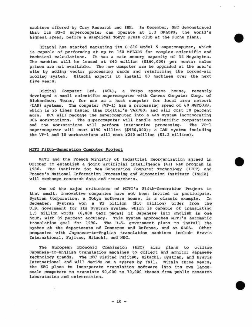
machines offered by Cray Research and IBM. In December, NEC demonstrated that its SX-2 supercomputer can operate at 1.3 GFLOPS, the world's highest speed, before a skeptical Tokyo press club at the Fuchu plant.
Hitachi has started marketing its S-810 Model 5 supercomputer, which is capable of performing at up to 160 MFLOPS for complex scientific and technical calculations. It has a main memory capacity of 32 Megabytes. The machine will be leased at ¥40 million ($160,000) per month; sales prices are not available. The new computer can be upgraded at the user's site by adding vector processing cards and reinforcing the forced-air cooling system. Hitachi expects to install 80 machines over the next five years.
Digital Computer Ltd. (DCL), a Tokyo systems house, recently developed a small scientific supercomputer with Convex Computer Corp. of Richardson, Texas, for use as a host computer for local area network (LAN) systems. The computer (VP-1) has a processing speed of 60 MGFLOPS, which is 25 times faster than Digital's VAX780, and will cost 50 percent more. DCL will package the supercomputer into a LAN system incorporating DCL workstations. The supercomputer will handle scientific computations and the workstations will perform interactive processing. The VP-1 supercomputer will cost ¥190 million ($950,000) ; a LAN system including the VP-1 and 10 workstations will cost ¥240 million ($1.2 million).
MITI Fifth-Generation Cc»puter Project
MITI and the French Ministry of Industrial Reorganization agreed in October to establish a joint artificial intelligence (AI) R&D program in 1986. The Institute for New Generation Computer Technology (ICOT) and France's National Information Processing and Automation Institute (INRIA) will exchange research data and researchers.
One of the major criticisms of MITI's Fifth-Generation Project is that small, innovative companies have not been invited to participate. Systran Corporation, a Tokyo software house, is a classic example. In December, Systran won a ¥2 billion ($10 million) order from the U.S. government for its Systran system, which is capable of translating 1.5 million words (6,000 text pages) of Japanese into English in one hour, with 85 percent accuracy. This system approaches MITI's automatic translation goal for 1990. The U.S. government plans to install the system at the departunents of Commerce and Defense, and at NASA. Other companies with Japanese-to-English translation machines include Bravis International, Fujitsu, Hitachi, and NEC.
The European Economic Commission (EEC) also plans to utilize Japanese-to-English translation machines to collect and monitor Japanese technology trends. The EEC visited Fujitsu, Hitachi, Systran, and Bravis International and will decide on a system by fall. Within three years, the EEC plans to incorporate translation software into its own large-scale computers to translate 50,000 to 70,000 theses from public research laboratories and universities.
- 10 -
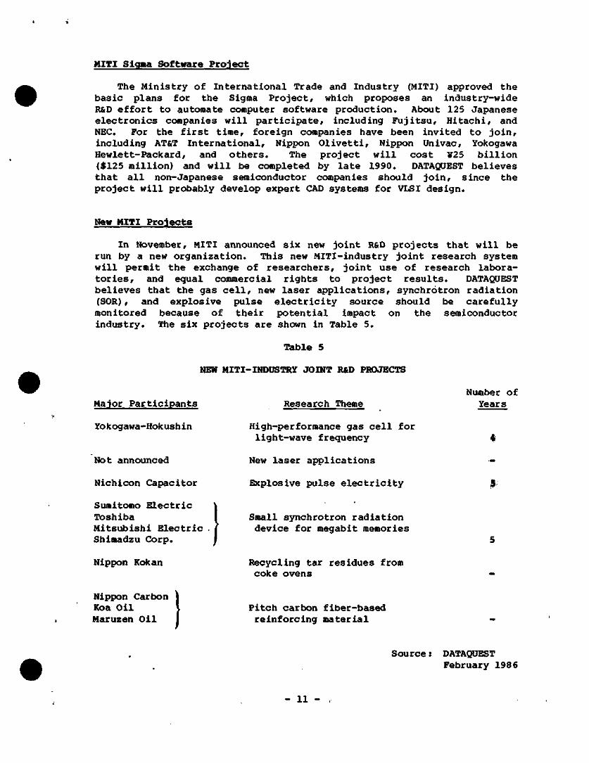
MITI Sigaia Software Project
The Ministry of International Trade and Industry (MITI) approved the basic plans for the Sigma Project, which proposes an industry-wide R&D effort to automate computer software production. About 125 Japanese electronics companies will participate, including Fujitsu, Hitachi, and NEC. For the first time, foreign companies have been invited to join, including AT&T International, Nippon Olivetti, Nippon Univac, Yokogawa Hewlett-Packard, and others. The project will cost ¥25 billion ($125 million) and will be completed by late 1990. DATAQUEST believes that all non-Japanese semiconductor companies should join, since the project will probably develop expect CAD systems for VLSI design.
New MITI Projects
In November, MITI announced six new joint R&D projects that will be run by a new organization. This new MITI-industry joint research system will permit the exchange of researchers, joint use of research laboratories, and equal commercial rights to project results. DATAQUEST believes that the gas cell, new laser applications, synchrotron radiation (SOR), and explosive pulse electricity source should be carefully monitored because of their potential impact on the semiconductor industry. The six projects are shown in Table 5.
Table 5
NEW MITI-INDUSTRY JOINT R&D PROJECTS
Major Participants
Yokogawa-Hokushin
Research Theme
High-performance gas cell for light-wave frequency
Number of Years
Not announced
Nichicon Capacitor
New laser applications
Explosive pulse electricity
Sumitomo Electric Toshiba Mitsubishi Electric Shimadzu Corp.
Small synchrotron radiation device for megabit memories
Nippon Kokan Recycling tar residues from coke ovens
Nippon Carbon Koa Oil Maruzen Oil
Pitch cartx>n fiber-based reinforcing material
Source: DATAQUEST February 1986
- 11 -
IC Card Research Coiiittee
The IC Card Research Committee, a study group involving MITI, the Ministry of Finance, and companies, reports that it will take about 10 years before smart cards become popularly available. Prices for IC cards combining an EPROM or EEPROM with an 8-bit MCU must decline to about ¥1,000 ($5), or one-tenth the current prices. DATAQUEST believes that prices will quickly decline, since most Japanese makers are already using standard cell technology to develop IC cards. The major obstacle will be institutional and public acceptance of the cards. We will issue a newsletter on Japanese IC card trends later this month.
MITI Bioelectronics Project
MITI announced that it will launch a 10-year national project in fiscal 1986 to develop bioelectronic devices. The project will focus on several themes, including analyzing the biochemical reactions of living organisms and the neural systems of lower animals, building molecular structures and thin-film materials, and performing ultrafine fabrication. The project is tentatively budgeted at $40 million, and will include work on biochips, biosensors, bio-resists, and biocomputers. DATAQUEST expects the major Japanese electronics and biotechnology companies to participate in the project.
NTT Artificial Intelligence and INS Computer
Nippon Telegraph and Telephone Corporation (NTT) is teaming up with foreign companies to develop semiconductors, value-added networks (VANs), and artificial intelligence. As shown in Table 6, NTT has recently signed four major agreements.
Table 6
NTT JOINT DEVELOPMENT WITH FOREIGN COMPANIES
Development Focus
Joint development and marketing of VAN services
Company
AT&T
IBM
TI & Motorola
Westinghouse ^ Stanford GTE Lab Xerox Batelle
Link-up Of IBM's System Network Architecture (SNA) with NTT's Digital Communications Network Architecture (DCNA)
2- to 3-year joint development of LSI substrates for INS Computer, artificial intelligence, and satellites
Artificial intelligence, semiconductors using new materials
Source: DATAQUEST February 1986
- 12 -
MPT Autaiiated Translation Telephone Project
The Ministry of Posts and Telecommunications (MPT) recently prepared a master plan to develop a translation telephone within 15 years and a translation telex system in 10 years at a cost of ¥100 billion ($500 million). The planning council, headed by Professor Nagano of Kyoto University, will prepare a concrete plan by April 1986. DATAQUEST believes that this project will be related to MITI's Fifth-Generation Computer Project and NTT's INS Computer, which are both focusing on automated translation and natural language entry technology. Semiconductor research will focus on speech recognition and synthesis, AI chips, and memory storage.
NASDA Inter-Satellite Laser Communications Project
The National Space Development Agency (NASDA) is investigating the use of lasers for intersatellite communications. For the experiment, NASDA chose two satellites: an observatory satellite orbiting the earth at 900km and a geostationary communications satellite orbiting at 36,000km. The distance between them is 40,000km. NASDA plans to develop GaAs lasers with 200mW output to transmit signals at 1 gigabit per second, or 10 times the existing capacity. Although Japan plans to use this technology for peaceful purposes, DATAQUEST believes that the U.S. Department of Defense will be interested in it for its Strategic Defense Initiative (SDI)—"Star Wars"—program.
NEW PRODOCTS AND TECHNOLOGY TRENDS
The following sections summarize the major semiconductor products and technology developments announced by Japanese companies during the fourth quarter of 1985.
Memory
Fujitsu—A 4K PROM with an output register and 40 percent lower power dissipation (MB7226RA-20L); 15ns access time; 70 milli-ampere power dissipation; sampling at ¥2,000 ($10); three packages available: 24-pin skinny DIP, 24-pin flat package, and 2 8-pin leadless chip carrier
A 1Mb CMOS mask ROM (MB831000) ; 150ns access time (earlier device with 350ns); 128K x 8-bit structure; TTL-compatible; 220mW power dissipation at operation and 275 milliwatts at standby; 1.7-micron design rule; priced at ¥5,000 ($25) for 500-unit orders
- 13 -
A 1Mb EPROM module; two leadless chip-carrier CMOS 512K EPROMs with their controller circuits into a 600mm wide, 30-pin dual in-line package; compatible with Fujitsu's 1Mb mask ROM; allows upgrading from 512K with slight change in PC board; 45mA maximum power consumption in operating mode and 15mA in standby; 250/300ns access times; sampling at V25,000 ($125); 30-pin DIP
Hitachi—^A hybrid bubble memory in a disk compatible with 8-inch flexible disk drives; nonvolatile, stable disk; 250K version (¥l60,000/$800) ; 500K version (5r200,000/$l,000) ; 1.2MB version (¥260,000/$l,300); Hitachi developing 4MB and 16MB versions compatible with 5-inch flexible disk drives in 1986 and with 3.5-inch drives in 1987
Conventional capacitance structure to be used in CMOS 1Mb DRAMs; preferred over "Trench-type" structure because of its predictability and higher yield factor; NEC to pursue Trench method
A Hi-BiCMOS 16K RAM (HM10480L) compatible with ECL RAMs; 16K x 1-bit structure; 350mW power dissipation during operation (half of ECL RAMs); 25ns maximum address access; 20ns minimum write-in pulse; priced at ¥4,000 ($20) in lots of 10,000
Matsushita—World's first 4Mb mask ROM (MN234001); capable of storing 3,500 Kanji characters; 4.2 million transistors on a 5.7 X 10.4mm chip; 1.4-micron design rule; double polysilicon wiring; NAN multigate memory cells and ROM code formed on depression mode transistors; 150mW power consumption during operation and 35mW at standby; 250 access time; operational character style and other programs stored in remaining 1Mb storage capacity; 16,000 characters of 16 x 16 dot size stored; 250ns access time; compatible with 512K x 8-bit and 256K x 16-bit type 5V power voltage; 150mW power consumption in operation and 35mW in standby; 40-pin plastic DIP; initial monthly production of 50,000 units; sampling at ¥5,000 to ¥10,000 ($25 to $50)
Mitsubishi—A 2,048-bit electrically alternative ROM that is compatible with multichannel service; for use in television and VCR tuning systems; gate insulator layer made of oxide and nitride films; 128 words x 16 bits; 14-pin dual in-line package; sampling at ¥600 ($3)
An NMOS 1Mb DRAM using planar 1.2-micron geometry; other sampling being done by Fujitsu, Hitachi, Matsushita, NEC, Oki, and Toshiba
Two CMOS SRAMs; 256K SRAM (M5M5256P) organized at 32K x 8-bits; 100/120/150ns; 1.3-micron CMOS process; sampling from ¥10,000 to ¥14,000 ($50 to $70); 64K SRAM (M5M5518XP) organized at 64K X 1-bit and 16K x 4-bits; 45ns access time; sampling at ¥8,000 ($40)
- 14 -
• NEC—A CMOS 64K SRAM (MuPD4362C) organized at 16K x 4-bits; 45/55/70ns access times; 1.7-micron design rule; double layer aluminum interconnect; 495mW power consumption during operation and llOmW at standby; priced at ¥5,000 ($25) for 45ns parts in orders of 1,000
A 4Mb DRAM using 0.8-micron design rule; to be introduced at ISSCC 1986; first samples from mid-1987
Entry with a 64K EEPROM during first half of 1986 due to huge growth seen for IC card market; others include Hitachi, Oki, and Mitsubishi
A CMOS 256K EPRQM (27C256AD) with 120ns access time (versus Intel's 200ns and Hitachi's 170ns); 1.2-micron design; 4.73 x 4.45mm chip size; 30mA power consumption during operation and 100mA at standby; priced at ¥1,500 ($7.50) in orders of 5,000
• Oki—Two single in-line memory modules; one organized in 262,144 nine-bit words and the other 8-bit wide; 120/150ns row address speed; 4 millisecond refresh period (256 cycles); 138mW power dissipation in standby and 2.75W at high speed
• Ricoh—Two CMOS 256K mask ROMs; 32K word x 8-bit; RP23C256H and RP23C257H pin-compatlble with Intel 27256 and TI 2564, respectively; 192.5mW power consumption during operation and llOmW at standby; 5V power supply; sampling at ¥1,000 ($5)
• Sharp—A CMOS 64K EPROM (LH5764J) using an original gate structure that hermetically seals the control gate, reducing data writing time by three-fourths; EPROM technology from Wafer Scale Integration; total bit writing time of 8 seconds; 1 millisecond write-in pulse width; sampling at ¥3,000 ($15); initial production of 50,000 monthly
TWO CMOS EPRQMs (LH5764J); 128K and 256K versions; 2-micron rule; 8K x 8-bit organization; 3.4 x 2.5mm chip size; 28-pln dual in-line package; 200/250/300/450ns access times
• Sony—A 512K NMOS nonvolatile memory (CXK1005P); P-channel aluminum gate NMOS process and 32-word x 16-bit structure; 20mW power consumption; 5V power supply; 16-pln plastic DIP; for use as electronic selector for televisions, VCRs, and POS terminal memories; data can be rewritten 100,000 times; priced at ¥700 ($3.50)
A CMOS 64K SRAM with high-speed processor for signal processing; 45/55/70ns access times; 64K x 4-blt structure; 2-mlcron design rule; double poly, double aluminum CMOS technology; 22-pln plastic or DIP; 275mW power dissipation during operation; signal processor with processor and multiplier that can perform arithmetic operation for 28-bit word digital signal with 125ns
- 15 -
command cycle; 36-bit arithmetic possible by combining two processors and one multiplier; multiplier usable as 32 x 16-bit adder/multiplier with 75ns multiplying time
• Suwa Seikosha—Three CMOS 1Mb mask ROMs using 1.8-mlcron geometry asynchronous ROM (SMM63100C) with 250ns access time, 30mA power consumption, and 28-pin plastic DIP; synchronous ROM (SMM23100C) with 16mA consumption, 450ns access time, and 28-pin plastic DIP; synchronous ROM (SMM733100C) with 450ns and 40-pin plastic DIP; sampling from ¥3,000 ($15)
• Toshiba—Mass production of CMOS 1Mb ORAMs at Oita plant from April 1986 at rate of 1 million units monthly; 1.2-micron design rule; 4.4 x 12.3mm chip; 2.2 million transistors; 100/120ns speeds
A 4Mb DRAM using 0.8 micron design rule; to be introduced at ISSCC 1986; DATAQUEST notes that American OEMs have already received samples
Application-Specific Memory (ASM)
• Mitsubishi—A multifunctional CMOS communication control memory for television and VCR remote controls; IK x 8-bit ROM, 32-word X 4-bit RAM, and two stack levels; 2.2 to 5.5 voltage range; 37.9 and 40 kHz; 30-pin shrink DIP package; sampling at ¥350 ($1.75)
IC Cards
• NEC—An IC card read-write terminal for banks, financial institutions, distributors, transportation companies, hospitals, and recreational businesses as information and access sources; N5256-40 card reader (¥l20,000/$600) and N5256-90 code key pad (¥l00,000/$500); card with 8-bit MPU and 64K ROM (¥l7,500/$87.50 in units of 10,000); card with 8-bit MPU and 16K ROM (¥5,000/$25 in units of 10,000).
• Nippon Shinpan/Visa Japan—Formal tie-up of Visa Japan and Japan's largest credit card company consisting of 21 credit card companies; a new Nippon Shinpan-Visa Card to be issued for shoppers; indirectly linked to Toshiba-Visa joint development of a Super Smart (IC) Card
• Toshiba/Visa International—Agreement to jointly develop a multifunctional IC card, the "Super Smart Card," equipped with number keys, liquid crystal display, and battery; for purchasing and banking transactions; no reading terminal to be required; prototype by summer 1987
- 16 -
Microprocessors/tlicrocontrollers
• Fujitsu—A CMOS 4-bit MCU with built-in prescaler, PLL synthesizer, A/D converter, and LCD driver for digital tuning systems; priced at ¥980 ($4.90) for 5,000-unit orders
• Hitachi/^otorola—Jointly developed 68HC000 version of Motorola's 68000; sampling since November 1985; 8/10/12.5-MHz versions; ceramic 64-pin dual in-line or 68-pin grid array; 200mW power consumption at 12.5 MHz; production at Motorola's Austin, Texas, plant and Hitachi's Musashi plant
• Hitachi—A 16-bit director memory access (DMA) controller (HD63450); capable of transferring data at 6.25 Mbytes per second; CMOS peripheral device for 68000; 6/8/10/12.5-MHz versions; 500mW power consumption; sampling at ¥12,800 to ¥17,500 ($64 to $87.50)
A CMOS direct memory access controller with 12.5 MHz-operating frequency (HD63450); DIP model sample priced at ¥16,900 ($84.50) or ¥9,900 ($49.50) in lots of 1,000; PGA model sampling at ¥17,500 ($87.50) or ¥12,000 ($60) in lots of 1,000; 6/8/10-MHz versions available; pin-compatible with Hitachi's NMOS version; 2-micron aluminum double-layer technology; 500mW power consumption; 64-pin ceramic dual in-line or 68-pin PGA packages
A OMOS 8-bit MCU (HD63705Z) in the 6305 series; built-in A/D converter of 8-bit x 8 channels and dual port RAM; 1/1.5/2-MHz versions; sampling at ¥3,200 to ¥3,600 ($16 to $18)
• Mitsubishi—A proprietary 32-bit MPU planned for 1987; also plans to second source Intel's 32-bit
A CMOS 16-bit single-chip MCU; 500ns command execution time; memory-mapped I/O system to facilitate future serialization; 64 basic commands and I/O ports; 2-micron CMOS process; 8K ROM and 512K RAM; eleven 16-bit built-in registers; 9.26 x 7.50mm chip; production model with built-in ROM to be 9 x 7mm chip; undergoing evaluation with sampling in fall 1986; shipments and development support system from second quarter 1987
Five control ICs for Winchester-compatible disk drives; two S-micron read/write ICs; M51835FP for controlling two magnetic heads; M51838PP for four heads; pulse-peak-detection IC (M51836FP) for converting lead circuit signals into pulses; access servo device (M51829FP); pre-drive for 3-phase AC brush-less motors (M51718PP/GP); sample prices of ¥1,300 ($6.50) for read/write ICs, $5.80 for pulse peak detection IC, and $1.86 for access servo IC and motor pre-driver; 16- to 32-pin packages
• NEC—A multifunction CMOS 4-bit MCU incorporating controller and driver for luminescent display tubes and 6K mask ROM (MuPD75206); 0.95 minimum instruction execution time; piggyback EPROM on MuPD75CG208 model; sampling at ¥15,000 ($75)
- 17
A 32-bit MPU {V60/70 Series) with a floating-point processor; 325,000 elements, or 50,000 elements more than Intel's 80386; sub-model 70 witti floating-point processor and peak processing capability of 5.3 MIPS; incompatible with Intel's 80286/386
V40 and V50 MPUs designed to compete with Intel's 80186 and 80188; 101 types of instruction sets; CP/M and MS-DOS operations; nine peripheral circuits, including a 4-channel DMA controller and 8-level interrupt controller; serial interface and programmable wait functions; 250mW power dissipation; 24 V30 MPUs reducible to seven V50 MPUs in a personal computer; sampling at ¥8,000 ($40) for V40 and ¥10,000 ($48) for V50
A higti-speed diagram processing system built around a non-Von Neumann MPU, consisting of a scanner, personal computer, laser printer, and image processor; capable of processing images and diagrams at 10 times most superminicomputers; functions include expansion and contraction of diagrams and characters, automatic conversion of diagram sizes, and unifying character widths; processing speed of 8 seconds per frame (1,100 x 800 dots)
A CMOS 8-bit single-chip MCU (MuPD78312) with twice the performance of Intel's 8096; for real-time control of high-speed printers and car engines; 16-bit ALU and register that performs 16 X 16-bit operation in 3.2ms and 32/16-bit division in 8.4ms; 0.5ms minimum instruction execution time; 30mW power dissipation; sampling at ¥2,000 ($10) in lots of 10,000
A real-time clock MCU (MuPD4990C) for use in personal computers, facsimiles, word processors, and other office equipment; interrupt function that stops sending data to the MCU during designated time frames; 500-KHz clock input frequency; priced at ¥400 ($2) in lots of 10,000
A CMOS general-purpose MCU for serial data transfer; designed for V Series MPUs; converts parallel data into serial data and vice versa; 1.5-Mbytes transmission modulation speed; 75mW power dissipation during operation; multi-protocol operation (bit- and character-oriented protocols); simplified system configuration that includes baud rate generator and digit:al phase lock loop circuits; 1.6-Mbytes transfer modulation speed; 75mW power consumption; priced at ¥5,000 ($25)
• Okayama Science University/Kobe University—A 256-element parallel processing architecture MPU; processor element (PE) with Z8, 2-Kbyte RAM, 256-Kbyte RM4; 8-bit input bus and 1-bit serial output bus
# Oki—A single-chip 8-bit MCU (80C59) featuring 16K ROM, 256-byte RAM, and 16-MHz operating speed; for multitasking control applications in telecommunications, industrial automation, instrumentation, and automotive skid control systems; capable of
- 18 -
addressing 64K bytes of data memory and program memory; priced at »3,000 ($15) in lots of 1,000 to 5,000; $3,500 tooling charge per instruction set for minimum 10,000-unit orders
A CMOS 8085A-version 8-bit MPU (MSM80C85A-2) manufactured under Intel license; 5.0-MHz operating frequency with 20mA power dissipation; power down current less than 7mA (compared to 170mA for NMOS version); 40-pin plastic DIP or 44-pin plastic flat package; priced at ¥1,500 ($7.50) in lots of 100
High-speed CMOS MPUs capable of operating at 8 MHz; MSM80C86-2 with 16-bit data bus; MSM80C88-2 with 8-bit bus; h»oth with 20-bit address bus allowing access up to 1-Mbyte RAM; 24 operand addressing modes; fourteen 16-bit registers; both in 40-pin plastic DIP, 40-pin ceramic DIP, and 44-pin LCC packages
• Sharp—A voice pitch control IC (IR3R41) developed with VSC Limited of the United States; sampling at ¥700 ($3.50)
NMOS and CMOS 8-bit voice recognition MPUs; 40-pin DIP or 44-pin quad flatpack; CMOS version sampling at ¥3,000 ($15); NMOS version at ¥2,000 ($10)
• Sony—TWO 4-bit CMOS MCUs (SPC500 series); CP5048 for mechanical and servo control of VCRs and 8mm videos; 8K ROM and 284 x 4-bit RAM; 1.9ms command cycle time; priced at ¥30,000 ($150); CP5040 for piggyback and evaluation modes; 8K external EPROM; ¥900 ($3) ; 5V power source; 64-pin piggyback and shrink DIP piggyback packages
V Series MPU shipments beginning; V20 featuring external 8-bit bus and 16-bit internal processing (CXQ70108); sampling at ¥3,000 ($15) for 5-MHz model and ¥3,500 ($17.50) for 8-MHz model; V30 series features 16-bit bus and 16-bit chip; sampling at ¥3,200 ($16) for 5-MHz version and ¥3,600 ($18) for 8-MHz model; both available in 400ns (5-MHz clock variation) and 250ns (8-MHz clock version) types
• Toshiba—Four CMOS serial input MCUs for use with Z80 MPUs featuring built-in circuitry for checking data accuracy, dual channel I/O terminals, and built-in ordering circuits; an asynchronous MCU (TMPZ84C42P) in 40-pin DIP for low-speed transmission; two asynchronous models (TMPZ84C40P/41P) in 40-pin dual in-line packages for high-speed, large-capacity transmission; a fourth model (TMPZ84C43F) incorporating features of Other three models packaged in 44-pin flat package; 800-Kbs maximum data transmission; 4-MHz operating frequency range; 4mA power consumption; sampling at ¥2,500 ($12.50)
Two CMOS LSIs for Multibus II interface under second-source agreement with Intel; model BAC84110 for bus control and MIC84120 for interruption control; sampling at ¥30,000 ($150) per kit
- 19 -
Digital Signal Processors (DSPs)
• Hitachi—Two graphic signal LSIs; graphic signal-reading LSI (HO63084) capable of reading graphic signals with CCD line sensor or facsimile sensor, correcting distortion, and translating into digital signals; reading speed of 5Mb of image signals per second; SOOmW power consumption; sampling at ¥7,000 ($35) or ¥5,000 ($25) in lots of 1,000; graphics signal-coding LSI (HD63085Y) capable of codifying/multicodifying MH, MR, and MMR codes of CCITT G3 and G4 standards; sampling at ¥24,000 ($120) or ¥16,000 ($80) in lots of 1,000
• Matsushita Technical Institute—A CMOS half-tone processor that offers excellent gradation and resolution while eliminating moire (ripple pattern); called Correction Density Assigrunent of Adjacent Pixels (CAPIX); 350ns maximum processing speed per picture element; processing of A4-size picture in 1.5 seconds; 65,536 pixels horizontally and unlimited pixel count vertically is possible; 2.5-micron CMOS process; 22,300 elements; sampling at ¥10,000 ($50) from early 1986
• Mitsubishi—Remote control signal processor (M50461-SP) for television, VTR, and other consumer goods; 3mW power consumption; 5V; 12 X 8 key matrix; 37.9-KHz frequency; IK x 8-bit ROM; 32-word X 4-bit RAM; sampling at ¥350 ($1.75)
• NEC/Oki—A jointly developed CMOS signal processor compatible with NEC's NMOS MuPD7720 processors; 16 x 16-bit parallel multiplier, 512-word X 23-bit instruction program ROM, and a 128-word X 16-bit RAM; marketed as NEC MuPD77C20 and Oki MSM77C20; priced at ¥3,000 ($15)
• Sharp—A signal processor for stationary head digital audio tape records; sampling since October
• Sony/TOshiba—Two CMOS image processors for still-image graphic reproduction for compact digital audio disks; color graphic control for processing video signals from disks and reducing adapter size for still graphics by three-quarters; graphic data processing LSI with 13,000 elements in a 100-pin package; video synchronization signal-generating LSI with 2,000 elements in a 44-pin package
• Tokyo Sanyo—A telephone dialer LSI (IiC7360) with both tone and pulse dialing modes; bi-directional switching; automatic and manual mode switching
A digital servo controller for hard disk spindle motors (LC7990); sampling at ¥700 ($3.50)
• Toshiba—Three LSIs for character-multiplex television sets based on recently adopted Japan Broadcasting Corp. method; TA8610N waveform equalizer compensates for waveform distortion in incoming character multiplex signals; bipolar LSI using
- 20 -
advanced nitride self-alignment (ANSA) process; 2,300 linear devices, 1,300 gates, 42-pin shrink DIP package; TC9016N data recognition and calculating that translates signals into video output; TC9017C graphic display control device that eliminates noise in output signal; both data and graphic ICs are CMOS, 2-micron rule; 64-pink shrink DIP; sample kits priced at ¥20,000 ($80)
A single-chip LSI for compressing and extending digital signals (T7615 in Japan and United States, T7625 in Europe); 33,000 elements; 20-micron CMOS process; 40mW power consumption; sampling from January at ¥30,000 ($150); capable of doubling transmission speed to 32 Kbs
A CMOS voice recognition LSI capable of recognizing 40 words with 80 to 90 percent accuracy; 6mm square chip; conversion from voice data to 4-bit digital data; 4.5mA operating time; 67-pin flat package; sampling at ¥2,000 ($10)
implication-Specific ICs (ASICs)
• Fujitsu—Two CMOS gate arrays series (1.0ns and 1.4ns per gate delay time); 1.0ns series available in two models: 20,000-gate UH series using 3-layer metal wiring, and UM series that is available in 10,000-gate, 12K RAM and 15,000-gate, 6K RAM models; 15ns RAM access time; UH unit price of ¥35,000 ($175); 135/179/256-pin pin grid array packages; the 1.4ns series consisting of AVB (2,640 to 8,000 gates), AV (5,022 gates), and AVM; 2,052-gate AVB priced at ¥1,200 ($6) for 10,000-unit orders; 5,022-gate AV priced at ¥3,000 ($12)
• Hitachi Cable—A multiplex transmission LSI developed with bi-CMOS gate arrays (HD27A026); capable of time-division multiplex transmission up to 64 points; 64-pin dual in-line package; 50mA; 5V power supply; optical data multiplex transmission module (OMX-6400) for building two-way transmission unit capable of transducing parallel signals of 64 points to serial signals by time-split multiplexing
• Mitsubishi—A CMOS gate array utilizing variable track master slice (VTM) technology; three times the integration density of conventional gate array products; 11.96 x 7.72mm chip with 215,000 transistors; interconnect channels replaced by channels filled with transistors that can be used for wiring or circuits; 35,900-gate prototype; 1,496 x 72 organization; co inmercia l iza-tion by June 1986
• NEC—Two ECL gate arrays; 5,000-gate version (uPB6350) and 4,000-gate version (uPB6340); 1.4-micron wide emitter; 0.43ns input buffer delay time; 1.32ns output buffer delay time; signal I/O levels correspond to 10OK, lOK, and TTL levels; development cost for 5,000 gates (¥15,000/$75,000) and unit price of
- 21 -
¥50,000/$25 for lots of 1,000 units; 4,000-gate development cost (¥9 million/$45,000) and unit price of ¥40,000 ($200) for 1,000-unit lots; maximum of 156 and 72 I/O terminals, respectively; 132-pin and 208-pin pin-grid array pacIcages
Two CMOS gate arrays with option to incorporate RAM, ROM, or both; 2,240-gate array with 2K memory (MuPD65023); 4,400-gate array with 4K memory (MuPD64043) ; 64 word x 9-bit RAM and 128 word X 9-bit ROM; 20ns access time for RAM; nonrecurring engineering (NRE) cost of ¥6.8 million ($34,000) for MuPD65023, which is priced at ¥2,900 ($14.50) in 5,000-unit lots; NRE for ¥9.3 million ($46.50), which is priced at ¥7,200 ($36) for 5,000-unit lots
A CMOS gate array series with 10 models, using 72- and 132-pin plastic pin grid array packages (except 2,100-gate array that only comes in 72-pin package); 2,100/3,700/4,700/7,100-gate 1.4ns arrays; 2,100/3,300/4,100/6,500/8,000/11000-gate 2.0ns arrays; 8,600/10,000/15,000/20,000-gate 1.4ns array devices in final development phase
A standard cell series; 1.5-micron CMOS process; 1.4ns internal gate delay time; 130 function blocks already demonstrated with gate arrays, including buffer, stable multivibrator, Schmitt trigger circuit, and pull-up/pull-down resistor; maximum of 17,000 gates to be expanded to 25,000 gates in 1986; 256 maximum signal terminals; 20ns maximum RAM access time; 30ns maximum ROM access time; ¥10 million ($50,000) development cost for 3,000 gates, with minimum lot of 100,000 units priced at ¥800 ($4) each
Oki—A standard cell library (MSM91000) with 84 logic cells, RAMs, ROMs, and PLAs in variable bit lengths; 2-micron CMOS process; 1.7ns gate delay times; RAM access time of 30ns; available in flat, DIP, PLCC, and pin grid array packages; 12 week development time from logic simulation to evaluation sample shipment for 2,000-gate devices
Oki—Standard cell library (MSM91000 series); up to 25,000-gate devices; 208 terminals; 2-micron CMOS process; 1.5ns access time; 4.5 to 5.5 volts; 2-layer metal
Sanyo—Standard cells incorporating LC9500, TTL74, and LC9500 series; nonrecurring engineering (NRE) cost of ¥4 million ($16,000) for 500 to 1,000 gates, and ¥6 million ($24,000) for 3,000 to 4,000 gates
- 22 -
CAD Systems
Hitachi—Two-dimensional CAD simulator using semiconductor laser; color graphics display; animation display of current and voltage characteristics and current output; check for defect densities; AlGaAs/InGaAS laser used; several minutes processing time using S-810 supercomputer; circuit evaluation time reduced from several months to two weeks
NEC—A CAD system (LOMEO) that converts circuits directly from printed circuit boards to LSI circuits, reducing design time from several months to one week (including check-out time for the design engineer); system consisting of ACQS 1000 host computer and workstations; capable of handling 50,000 functional blocks equal to 200,000 gates, essentially any type of custom IC; no commercialization plans
Optoelectronics
• Fujitsu—An avalanche photo diode for optical communications in 1.55 micro band range; compound material of indium, GaAs, and phosphor with buried indium phosphor for signal amplification; capable of 2Gb/sec transmission rate and 300km repeaterless transmission; 20 GHz sensitivity; 70mA leak current
« Hamamatsu Photonics—Silicon photodiode array with 46 elements; 190 to l,100nm wavelength; 4.4 x 0.94 x 0.94 per circuit; 1.0mm pitch; 40/48-pin ceramic DIP; S2311/12/13/17/18/19 series
• Hitachi—A 1.55-micron band laser diode developed using conventional buried heterostructure method (HL-1521A); distributed feedback (DFB) type diodes currently by others still several years away; 100km repeaterless transmission capability, twice that of 1.3-micron diodes; 50mW optical output; 30mA threshold current; sampling at ¥350,000 ($1,750) in lots of 100
A new method for fabricating distributed feedback laser diodes for long-distance, large capacity optical communications; etching performed before crystal layers are formed on the substrate, reducing layer erosion and improving shape precision; 90 percent chip yield achieved
• Matsushita—A coherent light semiconductor laser; 0.9-MHz frequency spread achieved using a resonator
• Mitani Electronics—A static induction photo transistor (SIPT) developed by Tohoko University Professor Junichi Nishizawa, with 1,000 times the sensitivity of bipolar photo transistors; minimum light detection sensitivity of one nano-watt per square centimeter at 655nm; 3- to 5-volt operating range; 400 x 400-micron surface area; capable of detecting 40 to l,100nm light; for use in camera exposure meters
- 23 -
• NEC—World's first AlGalnP (aluminum-gallium-indium-phosphor) .6nm-band semiconductor laser capable of continuous
oscillation at room temperature; air contamination reduced due to a refined MOCVD process; double heterostructure formed using a new crystallization process; 35mA oscillating threshold current at room temperature; 4.1kA-per-square-cm oscillating threshold current density; first NEC AlGalnP laser introduced in 1982
4> NTT—A 10-Gbs distributed feedback laser diode capable of converting 144,000 lines of telephone information into optical signals in 1 second (equivalent to 625 million kanji characters) ; superlattice structure using 60 alternate layers of InGaAs and InAlAs; parasitic capacitance reduced by eliminating 90 percent of the buried layers sandwiching the active layer, changing the crystal substrate from N-type to P-type, and impregnating the active layer with zinc dopants; lOmW DFB laser with 10-Gbs optical signal conversion capacity
(It Oki—A laser diode with 2.1-watt output that can theoretically be improved to 20 watts; silicon injected into the laser diode GaAs material to prevent light re-absorption by the diode itself; for use in communications satellites and ships
• Sharp—Two semiconductor lasers based on Sharp's VSIS structure; maximum light output of 200mW continuous operation; lOOmW output power achieved by using three channels and 50-micron interval between channels; 830nm oscillation wave length; low cap hermetic package (LT090MD) and low cap hermetic package with fins (LT09CMF)
• Stanley Electric—Six new high-power infrared LEDs; three narrow-angle models: 80mW/sr. 850nm, 30mW/sr. 880nm, and 25mW/sr. 950nm; three wide-angle models (30 to 50 degrees): 30mW/sr., 20mW/sr., and 15mW/sr.; 80mW/sr. version sampling at V2,000 ($10)
• Toshiba—A 670 to 680nm AlGalnP semiconductor laser using MOCVD process; GaAs substrate; 100mA current; lOmW power output
Image Sensors
Japanese companies are rapidly moving into the charge-coupled device (CCD) field because of its application to 8mm video cameras, optical readers, and inspection and monitoring devices. The major participants in this area include Matsushita, Mitsubishi, NEC, Sanyo, Sharp, Sony, Texas Instruments Japan, and Toshiba. CCDs generally sell for ¥10,000 to ¥20,000 ($50 to $100) and offer high profits.
• Matsushita Electronics/Matsushita Electric—A jointly developed contact bipolar image sensor; 325aim (A3 size) sensor length; 5,120 dots; 0.26ms/line reading speed; 10-chip parallel output
- 24 -
Mitsubishi—A contact image sensor for office automation equipment; 256mm reading width; 8 lines/mm resolution; 2.5 millisecond reading speed; 43 x 36 x 293mm dimensions; sampling at ¥100,000 ($500); for facsimile machines and electronic blackboards
NEC—A CCD color image sensor for NTSC (uPD3520D); 1/2-inch 5CD sensor with 220,000 graphic elements and 8-lux maximum sensitivity; sampling at ¥30,000 ($120); initial monthly production of 10,000; 100,000 units monthly in fiscal 1986
Sanyo—Four CCD black and white solid-state image pickup devices: LC9911 (2/3-inch NTSC), LC9921 (1/2-inch NTSC), LC9923 and LC9925 (PAL); for pricing see I.C. ASIA, November 14, 1985, page 10
Sigma Corporation—A wet aluminum etching device for mass producing 10-inch liquid crystal display (LCD) boards and high-resolution image sensors for facsimiles
Toshiba—A full color copier CCD; 780nm; 617 x 470mm; A4 paper; 500W power consumption for copier; copier priced at ¥2.8 million ($14,000)
Gallium Arsenide
Japanese GaAs makers are beginning mass production of 3-inch wafers in anticipation of full-scale production of GaAs ICs, semiconductor lasers, and GaAs FETs. Sumitomo Electric, Shin-Btsu Handotai, Mitsubishi Monsanto, Nippon Mining, Showa Denko, and others are ramping up production in 1986.
•i Fujitsu—A 4K GaAs SRAM prototype with 1.7ps access time; 27,000 transistors on a 5.5 x 3.7mm chip; new transistor formation process that implants ions into GaAs substrate through a thin aluminum nitride layer; ions impeded by nitride layer, forming shallow channels for electron path
* Matsushita—A GaAs 1-GHz prescaler with 3.2mA current dispersion at 1 GHz; 1.0 x 1.2mm chip integrating 298 FETs, 56 resistors, and 68 diodes; uses 5V power supply, 1-GHz signal switchable at 128/130/256/258; double-phase-drive source-coupled FET logic (SCFL); each FET constructed using ion injection on a GaAs substrate; uses boundary wall smoothing techniques; 27 x 25-micron cell size; 3.0ns access time; sampling at ¥3,000 ($15); for use in mobile radio equipment
A 300mV GaAs Hall device (IH005) using high-purity GaAs and a newly developed diffusion process that improves electrode materials and stabilizes ion implantation and annealing; 0.35mm square chips; 1.5 x 2.9 x 1.1mm miniflat packages that can be direct soldered or installed by automatic taped or magazine feeding; 750-ohm input resistance; sampling at ¥80 ($0.40)
- 25 -
• Mitsubishi—A 12-GHz amplifier module for improving reception quality and capability of satellite relays; two GaAs FETs, capacitors, and other devices on th ic I t - f i lm ceramic substrate; 27 X 25.4 X 5.8mm pacIcage; 18dB gain with 2.2 to 2.4dB noise index; the FA12201 for 11.7 to 12.2-GHz business communications (¥7,500/$37.50); FA12202 for 12.2 to 12.75-GHz DBS relays (»8,000/$40); FA12203 for 11.7 to 12.5-GHz for European satellites (V8,000/$40); 50mA consumption
A 4K GaAs SRAM with 2.5ns access time; IK x 4-bit structure; 3.3 X 3.2mm chip; 200mW power dissipation; developed under MITI's Supercomputer Project; other companies with 4K GaAs SRAMs include NTTf Fujitsu, and Hitachi; Mitsubishi now worIcing on 16K GaAs SRAM
A GaAs prescaler with 1-GHz operating frequency and 2.9inA; 5V power source; the demultiply switchable at 128/129; source-coupled FET logic (SCFL) circuit and recessed FET gate structure; 444 elements on 1.0 x 1.1mm chip; for use in mobile radio equipment; source-coupled FET logic and Mitsubishi's proprietary shallow-recess-structured FET possessing surface n+ layer; 1.2-GHz maximum operating frequency at 4mA, 1.56 GHz at 5.6mA, and 1.9 GHz at 9.2mA
* MITI Electrotechnical Laboratory—^A GaAs complementary FET; heat generation suppressed, allowing development of 4Mb-level GaAs devices; new design (SIS-FET) eliminates need for special insulating film between p-type and n-type transistor on a uniform GaAs substrate
Mitsubishi Monsanto—^Mass production of 3-inch nondislocated GaAs wafers from January 1986; initial monthly production of 500 wafers, expanding to 2,000 wafers monthly by second half of 1986; vertical magnetic (VIA) imprinting system developed by NTT in 1984 used to attain low-temperature gradient and automatic diameter control for LEG process
i NEC—An InGaAs/InAlAs HEMT with 440mS/mm conductance; InGaAs channel; InAlAs carrier layer; higher mobility than conventional GaAs/GaAlAs HEMTs
• NTT Atsugi Lab—A GaAs FET; 300nm undoped GaAs active layer, 30nm AlGaAs layer, 5iun GaAs storage layer; n-type silicide and two-layer GaAs/n+Ge; p-type silicide; source and drain fabricated using n-type silicon and p-type beryllium; 125ps at 300 degrees Kelvin; 330 MHz; 3.5mW/gate
* Sony—A GaAlAs/GaAs high-electron mobility transistor FET (HIFET) fabricated using metal organic CVD; Model 2SK-676 with 200-fflicron wide gate for DBS and Model 2SK-677 with 300- nicron wide gate for television receivers; same structure as Fujitsu's HEMT; 1.2dB noise at 12 GHz and lldB standard gain; sampling with ceramic package at ¥100,000 ($500)
- 26 -
Sumitomo Electric—Mass production of 3-inch GaAs wafers; 3,000 wafers monthly capacity; computerized liquid encapsulated Czochralski (LEC) pulling method used to produce uniform crystal growth; dislocation defects reduced by lowering temperature gradient during pulling and by controlling vertical and lateral movement
A GaAs substrate with indium additive reduced by two-thirds; for use as material in optical ICs; pilot production of 2-inch ingots beginning; computerized system used to control the temperature for ingot growing, allowing relatively defect-free ingots; plans to develop 3-inch ingot by 1987 and commercial optical ICs within five years
Joaephson Junctions
NO major announcements.
New Electron Devices
• Fujitsu—A superlattice transistor with a Ips theoretical switching speed; called resonance tunneling hot electron transistor (RHET); entire NOR circuit on a single RHET, reducing arithmetic logic circuits to one-seventh current levels; combination of a resonance tunnel diode-type element with negative resistance characteristics; quantum well of AlGaAs and GaAs superlattice structure as emitter wall; output twice input frequency; operating from low frequencies to 100 GHz; commercial use 7 to 10 years away; potential for replacing Josephson junction as next-generation chip
• Mitsubishi—A bio-device capable of transmitting electrons in a designated direction, potentially opening the way for bio-computers; a thin protein film (titochrome C molecules from a horse's heart) laid onto an aluminum-deposited glass substrate using the Langmuir-Brochette method; a fluorescent measuring system to confirm the molecular orientation of the protein molecules also developed
Standard logic
• Nippon Precision Circuits—A research project to develop an ultrahigh-speed molybdenum-gate OIOS device with a maximum clock frequency of over 100 MHz; goal of device three to five times faster than bipolar ECLs using 1.5-micron design rule; ECL speeds already achieved using 2.0- to 2.5-micron design rule; NPC's molybdenum technology jointly developed with Micro Power Systems
- 27 -
Bipolar Logic
• Fujitsu — flew Facoffl M-780 mainframe that is 6.7 times faster than M-380 series; a single-board CPU comprising 336 ultrahigh-speed VLSIs, including 3,000- and lO,OO0.-gate a:i« with 180ps delay time; high-speed RAMs and logic for buffer memory, and 256K SRAMs for 256^€byte main memory
• Tokyo Institute of Technology—A 3-layer bipolar transistor with performance of GaAs devices; top layer of silicon carbide in an amorphous state over two layers of silicon; potential use in supercofl Hiters and high-frequency communications equipment
• Toshiba—A bipolar MOSFET that withstands 1,000 volts (MG25N2CS); switching speed of 1.5 microamperes; used for controlling motors with 400 volts of input power supply; sampling at ¥15,000 ($75)
Linear/Analog
• Hitachi—Image recognition and processing CMOS A/D converter; 3.5^ sample/second; two RAM types (frame and index); 6.3 x 6.3mm chip; 80-pin flat package; 5V; 250mW power consumption
• Matsushita—A digital filter LSI (MN6618) for compact disk players; 96-order linear phase OlOS that processes stereo signals and handles two-fold oversampling; compatible with parallel and serial D/A converters; 42-pin chip; 75mW power consumption at 4.5V to 5.5V
• Mitsubishi—A voltage-controlled amplifier IC (M5241L) that controls two channels separately; for volume control in stereo receivers, VCRs, car audio equipment, and other audio-video uses; lO-pin, single in-line package; priced at ¥140 ($0.70) each
• Tokyo Sanyo—Three small hybrid ICs for car audio use; 50-micron design rule and high-density bent txsard; multiplex stereo demodulator with FM noise canceler (STK3400A/B) and 5-band graphic equalizer (STK3600); 7.5ffiffl profile
Discretes
Kyocera—A 4mm surface-mounted variable capacitor with l.Smm profile; 4.5x3.2mm chip size; rated at 25 VDC with temperature range of -25 C to +85 C degrees
Matsushlt:a—A MOSFET for use as digital switch in VTRs and other consumer products; 50ns switching speed; vertical diffusion self-aligned MOS structure capable of withstanding a surge of 1,200V; sampling at ¥30 ($0.15) each
- 28 -
A 2.45-GHz power MOSFET; V-shaped groove formed in the silicon substrate, allowing direct connection between source and substrate; for use in car telephones, wireless portable systems, and solid-state magnetrons for microwave ovens
• Mitsubishi—A prototype FET built using an organic polythiophene material; n-channel silicon wafer substrate covered with silicon oxide film; all electrodes arranged at 10-micron intervals as source and drain electrodes, then covered with polythiophene; for driving liquid crystal devices
• New Technology Development Corporation—A new electrostatic induction thyristor with 1-microsecond switching speed for use in miniature motors
• Sony—Two hetero-interface (HIPET) models for consumer electronics, using MOCVD method; sampling of 200-micron wide devices (2SK-676) from January and 300-micron wide version (2SK-677) from February; sampling at ¥100,000 ($500)
• Tokyo Institute of Technology—A prototype transistor fabricated by sandwiching four insulators and three metal films, each measuring two millionths of a millimeter in thickness; high electron mobility through the insulator layers; use of metal films and electron wave properties to increase speeds; potential use in optocomputer with several hundred times the capacity of current computers
New Processes
• Sharp—A new silicon-on-insulator (SOI) substrate using zirconium oxide single crystal as an insulator film; the zirconium oxide film sputtered onto a sapphire substrate in a vacuum chamber heated at 300 C degrees to obtain low power dissipation and high-speed device; prototype 1,000 Angstrom thick, high-quality insulator film on a 4-inch sapphire wafer; Sharp also working on cheaper silicon substrates
• Toyo Seimitsu—A photoetching method to draw 0.2mm lines on 96 percent alumina ceramic substrates of 0.635mm thickness; two-week turnaround; ¥3,000 to ¥5,000 ($15 to $25) for 80 x 80mm sheets; development on O.lmm ceramic etching under way
Materials
• Mitsubishi Electric/Mitsubishi Heavy—Thin-film diamond substrate experiments aboard U.S. space shuttle in 1987 to fabricate semiconductors for use in nuclear plants and satellites
• Sumitomo Electric—A diamond semiconductor for possible use in aerospace and other high-temperature, radiation-hazardous environments; plasma CVD used to develop n-type device; methane
- 29 -
and hydrogen heated to 800 degrees C to form plasma gas that is deposited onto a single-crystal synthetic diamond substrate; thin layer formed onto which phosphorous is doped at 1,000-ppm concentration; heat-resistant to over 500 degrees C for satellites, cars, and supercomputers
Toshiba—A new copper paste used in developing multilayer hybrid ICs; substrate cost lowered by 20 percent to 30 percent; printed resistor paste baked at 850 to 900 degrees C in normal atunosphere, then at 600 to 650 degrees C in nitrogen gas; half the material cost of silver palladium pastes
Manufactaring Techniques
Matsushita—A new film carrier technique, transferred bump tape automated bonding method, for fabricating double-layer LSIs; potential for combining up to three different ICs; prototype display drive LSI combined with high-voltage IC
A laser VLSI fault-diagnostic system for chips up to 0.8-micron rules and 4Mb DRAMs; 0.6328-micron helium neon laser radiated onto chip to compare electric current induced by the light with condition inside the chip; noncontact method that operates in normal atmosphere and avoids charge-up phenomenon produced by electron beam probing method
Ricoh—A new chip-mounting technology that inserts packageless ICs directly onto printed circuit board (chip-on-board method); increases PCB density two to four times and reduces production costs by 30 percent; experiments being conducted for facsimiles and printers at Ricoh's Hatano plant in Kanagawa; employs a special sealing resin with protective qualities of conventional plastic or ceramic packages; mounting method useful for memories, MPUs, peripherals, and gate arrays (of less than 160 pins)
Toshiba—A new process that directly joins silicon substrates to form transistors and diodes within two hours; capable of fabricating power ICs that can withstand high voltage and operate at high speeds; prototype bipolar MOSFET capable of withstanding 1,200 volts; planned commercialization of a 1,200V, 25-ampere bipolar MOSFET within one year
Manufacturing Equipaent
Hitachi—A microwave plasma etching system (M-206A) for 4Mb DRAM mass production; electron cyclotron resonance (ECR) etching system capable of 1.3- to 0.8-micron geometries; future improvements for 0.5-micron 16Mb DRAMs; etching speed of 30 to 50 wafers hourly; priced at ¥140 million ($700,000); deliveries from July; plans to sell 10 systems in first year, 70 to 100 systems in three years, and 200 systems over five years
- 30 -
A wafer stepper with 0.6-micron resolution (RA-IOIVL) for use in 4Mb DRAMs and above; capable of baking 10.4-square mm circuit in one cycle and handling 5-inch wafers; priced at ¥170,000 to ¥180,000 ($850,000 to $900,000)
A molecular beam epitaxial system that automates wafer-handling operations; for future-generation semiconductors such as GaAs chips, high electron mobility transistors (HEMTs), and super-lattice devices; automated wafer-handling and separate heating and crystal growing chambers that permit two different processes simultaneously; capacity of 10 to 12 wafers per day; sales from late 1986 at ¥150 million ($750,000)
Matsushita/Denko—A vertical CVD device producing uniform thin films on semiconductor wafers; vertical tunnel-shaped furnace used to introduce depositing gas from above; nitride coatings of 1,500 angstroms achieved; for use on 4Mb DRAMs and large wafers
NEC Anelva—A sputtering system for megabit VLSI production (ILC-1013MKII); priced at ¥180 million to ¥200 million ($900,000 to $1 million); designed for dual sputtering; double-cathode system for bias sputtering
Nippon Seiko—A multipurpose semiconductor lithography machine (TZ-310) with four functions: pattern generation, stepping, photo repeating, and direct writing; priced at ¥200 million ($1 million)
A molecular beam epitaxy system (MBE-8000) capable of processing seven 2-inch wafers or three 3-inch wafers simultaneously, resulting in throughputs of 70 2-inch wafers or 30 3-inch wafers per day; commercial plans not disclosed
Shimada Rika—An etching system combining reactive ion and plasma etching functions (EP-200RP); anode coupling for plasma etching cathode coupling for RIE; available from summer 1986 at ¥60 million ($300,000)
Clean Rooms
Seiwa Sangyo—Three dust-proof clean rooms; CBS-100 for Class 10 IC storage; CBS-200 for carrying ICs into Class 10 environment; CBS-300 for Class 100 rooms
Test Equipment
Advantest—An IC tester capable of testing 16Mb DRAMs (T333), 30-MHz speed and 16 megaword pattern generator; 32-megabit memories testable simultaneously using two test stations; priced at $585,000
- 31 -
Hochiki/MITI Physical and Chemical Research Institute—An exo-electron analyzer capable of measuring dirt accumulations on ICs; 0.2- to 0.35-micron ultraviolet ray used to gauge amount of electrons discharged from surface of semiconductor metal
Nihon Den-Netsu—An in-circuit IC tester (NCT-1200) with an automatic guarding system; capable of automatically testing for solder bridge, wrong parts, omitted items, defective elements, disconnected patterns, short circuits, and PCS problems
Packaging
Sumitomo Electric—An aluminum nitride ceramic for IC package tKJard substrate material; 10 times greater heat conductivity and better thermal expansion coefficient; being promoted by electrical and chemical makers as likely successor to alumina
Sheridan Tatsuno
- 32 -
Dataquest JAPANESE RESEARCH NEWSLETTER
JSIS Code: Newsletters 1985-1986, JSIA 1986-9
HOW TO SUCCEED IN ASICs; INDUSTRY LEADERS SHARE THEIR THOUGHTS
SUMMARY
Recently, several top American application-specific IC (ASIC)- vendors gathered in Silicon Valley to discuss the future prospects of the ASIC market. Although their strategies vary considerably, DATAQUEST observed a common theme running through their presentations. Most of the speakers emphasized that success in the ASIC market requires the following attributes:
• Leading-edge process technology {1.5-micron CMOS or below)
• Sophisticated CAD software using a common data base that can be run on a variety of personal computers
• Strong corporate commitment and service responsiveness
• Automated manufacturing and inventory control
The following are brief summaries of the major points made by six major ASIC vendors: LSI Logic, Monolithic Memories, Motorola, Oki Semiconductor, Texas Instruments, and VLSI Technology.
LSI LOGIC
Wilfred J. Corrigan, Chairman and founder of LSI Logic, observed that the crowded ASIC market leaves newcomers with no room for experimentation. Unlike LSI Logic, which could afford to learn through trial-and-error in 1981 since it was the only player, ASIC vendors must now be well prepared to survive the tough competition. What are the requirements for entering the ASIC market? Mr. Corrigan listed the following:
• Mainstream 1.5-micron CMOS process high yields
with high-density designs and
© 1986 Dataquest Incorporated Feb. 14 ed.-Reproduction Prohibited
The content of this report represents our interpretaion and analysis ol information generally available to the public or released by responsible individuals in the subject companies, but is not guaranteed as to accuracy or completeness It does not contain material provided to us in confidence by our clients Individual companies reported on and analyzed by DATAQUEST, may be clients of this and/or other DATAQUEST services This information is not furnished in connection with a sale or offer to sell securities or in connection with the solicitation of an offer to buy securities This firm and its parent and/or their otficers, stockholders, or members of their families may, from time to time, have a long or short position in the securities mentioned and may sell or buy such securities
Azabu Heights, Suite 711, 1-5-10 Roppongi, Minato-ku, Tokyo 106, Japan 1290 Ridder Park Drive / San Jose, CA 95131 / (408) 971-9000 / Telex 171973
Continuity of staff and products (no "flash-in-the-pan" efforts)
Defect-free chips within four to five weeks
Software and designs embedded into the CAD system
Strong service orientation
Domestic automated plants
Large investment ($30 million to $50 million required to become major player)
Long-term incentives for salespeople (due to long time from design to production)
Installed customer base
Mr. Corrigan said that LSI Logic competes with only a handful of the 200 ASIC vendors in the marketplace. Most ASIC companies are focusing on niche markets and lack the manufacturing and CAD capabilities to attack larger markets. He expects to see a major shakeout among these vendors soon.
MOMOLITHIC MEMORIES
Michael J. Callahan, Executive Vice President and Chief Operating Officer of Monolithic Memories, spoke briefly about MMI's approach to ASICs. Generally, MMI seeks high-volume products with unpredictable features that enable the company to capitalize on its programmable array logic (PAL) technology. Table 1 shows Mr. Callahan's characterization of the ASIC market segments.
Mr. Callahan believes that software must be an integral part of products across the ASIC spectrum. To achieve this goal, vendors must develop a CAD environment with a common data base. Moreover, standard product vendors must establish a separate ASIC manufacturing line (complete with automated inventory control) and a separate organization because of the totally different market demands placed on ASIC managers.
- 2 -
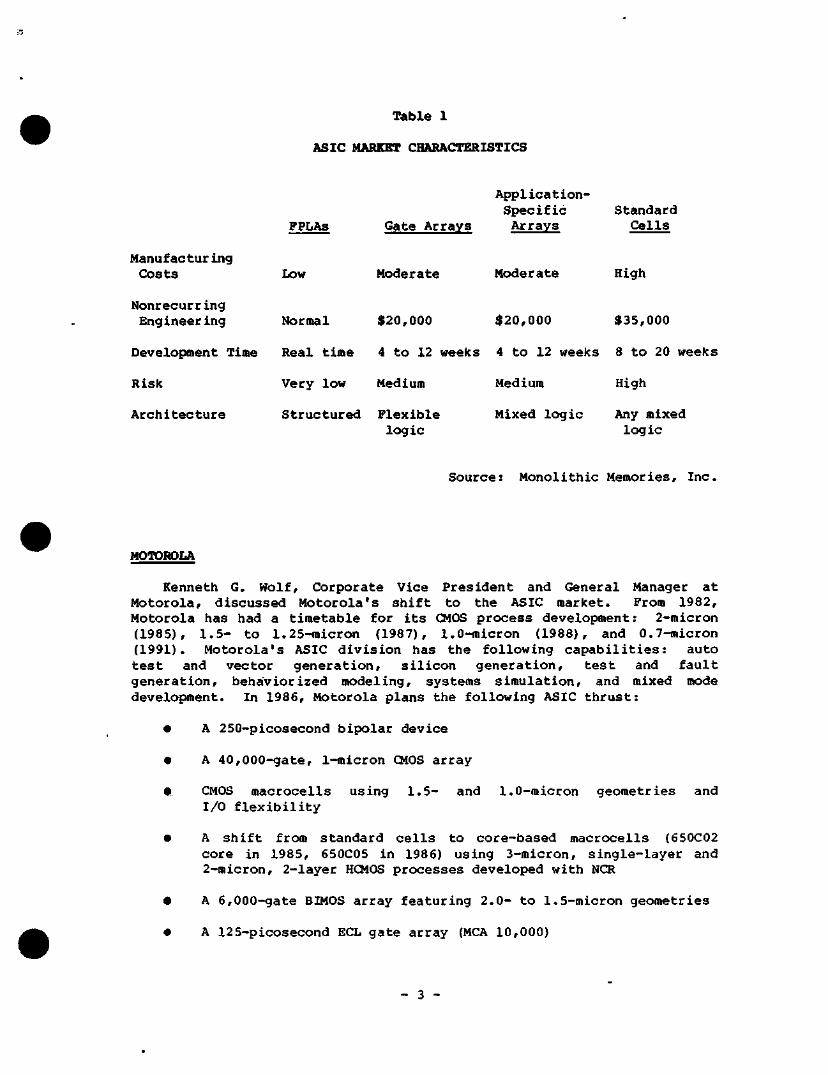
Table 1
ASIC MARKET CHARACTERISTICS
Manufacturing Costs
Nonrecurring Engineering
Development Time
Risic
Architecture
FPLAs
Low
Gate Arrays
Moderate
Application-Specific Arrays
Moderate
Standard Cells
High
Normal $20,000 $20,000 $35,000
Real time 4 to 12 weeks 4 to 12 weeks 8 to 20 weeks
Very low Medium Medium High
Mixed logic Structured Flexible logic
Any mixed logic
Source: Monolithic Memories, Inc.
MOTOROLA
Kenneth G. Wolf, Corporate Vice President and General Manager at Motorola, discussed Motorola's shift to the ASIC market. From 1982, Motorola has had a timetable for its CMOS process development: 2-micron (1985), 1.5- to 1.25-micron (1987), 1.0-micron (1988), and 0.7-micron (1991). Motorola's ASIC division has the following capabilities: auto test and vector generation, silicon generation, test and fault generation, behaviorized modeling, systems simulation, and mixed mode development. In 1986, Motorola plans the following ASIC thrust:
• A 250-picosecond bipolar device
A 40,000-gate, 1-micron CMOS array
* •
CMOS macrocells using 1.5- and 1.0-micron geometries and I/O flexibility
A shift from standard cells to core-based macrocells (650C02 core in 1985, 650C05 in 1986) using 3-micron, single-layer and 2-micron, 2-layer HCMOS processes developed with NCR
A 6,000-gate BIMOS array featuring 2.0- to 1.5-micron geometries
A 125-picosecond ECL gate array (MCA 10,000)
- 3 -
•ti A "one-month chip" goal in manufacturing
• Utilization of direct-write on wafer and dedicated masks
Motorola also plans to develop "silicon generators" to generate subfunctions to meet function specifications and to combine these subfunctions with standard cells. Mr. Wolf believes that silicon compilers will only be used for selected functions (such as ALUs) , not for all chips. Motorola is currently developing a silicon compiler.
OKI SEMICONOnCTOR
Jerry Crowley, President and Chief Executive Officer at Oki Semiconductor in Santa Clara, dispelled myths about the ASIC business by emphasizing the importance of automated manufacturing. He believes that "all creativity degenerates to hard work." Like memory makers, ASIC vendors must totally automate their design, manufacturing, and processes if they want to weather Japanese competition. To achieve this goal, Oki has pursued the following strategy:
• Developed an international CAD network with design centers in Japan, the United States, Europe, Hong Kong, and Singapore
« Developed six CAD software packages that run on IBM PCs (BINALY, ACTAS, FUNTASY, GALLOP, VILLA, and IDEAS)
• Installed a fully automated LSI packaging machine that features curing ovens, plastic molding, process control computer, die attach and bonding, and automatic inspection station
• Built an automated plant that transports 50 wafer lots daily using ceiling tracks to run deliveries
• Installed bar coding and transport in a peopleless ASIC plant using electron-beam, direct-write, and automatic inventory auditing
• Purchased a molding robot that handles 1 million units per month
Recently, Oki Semiconductor has achieved major ASIC breakthroughs using new automated techniques. These breakthroughs include:
• A standard cell 32-bit MPU (MVM6971) using 1.5-micron CMOS process and 224mm-sguare chip size; total design time was less than 12 months
• A 10,000-gate array (MSM78H000) using 2.0-micron CMOS process and dimensions of 99mm square and 154,450 square mils
» A digital signal processor (MSM6974) using 1.5-micron CMOS process, with dimensions of 124mm square and 191,981 square mils
- 4 -
Mr. Crowley concluded that most Japanese ASIC vendors are highly automated and, unless tJ.S. and European makers automate their ASIC design and manufacturing processes, they will forfeit the ASIC market to large Japanese vendors.
TBXRS INSTROMBNTS
William N. Sick, Executive Vice President of Texas Instruments, presented slides of TI's 1Mb DRAM (80,000 mil, 1-micron, 0.46-inch line) using 3-dimensional trench capacitors, and its 4Mb DRAM prototype using proprietary cells and a 0.384-inch length. The 4Mb DRAM was completed on schedule to the day using TI's new design automation system. Currently, TI has about 400 cells in its standard cell libraries and a second-sourcing agreement with Fujitsu to develop bipolar and CMOS gate arrays. TI aims at receiving 50 percent of its sales from four areas: ASICs, application processes, military, and CMOS and bipolar VLSI logic. In 1986, TI will use a 1-micron CMOS process from its ORAM work for ASIC devices, Mr. Sick said.
VLSI TECHNOLOGY
Alfred J. Stein, Chairman and Chief Executive Officer of VLSI Technology (VTI), believes that there are three keys to success in ASICs: a leading-edge process, software, and state-of-the-art manufacturing technology. VTI has established all three elements and is pushing its megacell approach. In the future, VTI will offer "full-chip composition," incorporating data path compilers, megacells, logic compilers, and ROM compilers. Common bus protocols will be used to eliminate interface circuits. These chips will feature fixed-height megacells, gate arrays, and standard cells on one chip. VTI is currently extracting megacells from standard products and inserting them into its megacell library, with the goal of developing cell-based structured arrays. In 1986, VTI will offer a 1.5-micron CMOS process, using double metal and poly. In 1987, it will have a 1.25-micron CMOS process using triple metal.
To market its ASIC devices, VTI has recently doubled its field sales force, opened new design centers, and signed agreements with Arrow Electronics, five European distributors, and three Japanese distributors. In addition, Mr. Stein said that Hewlett-Packard will market VTI's software.
- 5 -
QDESTION-AND-ANSWER PERIOD
After these presentations, the audience asked three questions:
« What are the keys to success in ASICs for major semiconductor makers?
• Wilf Corrigan (LSI Logic) believes that major companies must cannibalize their standard product markets with ASIC products, but they should also focus on developing MPUs and putting them onto boards. Start-ups have already replaced TTL-compatible peripherals.
Alfred Stein (VTI Technology) believes that the top software people and systems must be assigned to ASIC development, since software accounts for 10 percent to 15 percent of mask costs.
- Jerry Crowley (Oki Electric) believes that even the military market will see heavy ASIC competition. To survive, top makers must offer 10,000-gate arrays using 1.0-micron geometries and 100 MHz tolerances.
• Do ASIC vendors need to hook customers on their software?
—- Jerry Crowley believes that ASIC design software must be portable. Vendors should develop kits for various personal computers.
- Michael Callahan (MMI) believes that customers can support several major software packages, but not too many.
- Alfred Stein observed that ASIC users want a "total solution," not just software. The keys to success are technical support and first-time prototyping.
- Wilf Corrigan asserted that if vendors are genuinely serious about the ASIC market, they must appoint a Vice President of Software (like LSI Logic) who reports directly to the President. In addition, ASIC vendors must have a high proportion of software programmers. Of LSI Logic's 1,4 00 employees, 300 are programmers.
• Will major Japanese makers succeed in the U.S. ASIC market?
- Jerry Crowley observes that Hitachi, NEC, and other major Japanese companies are aggressively entering the market. He believes that the American perception of ASICs as a "protected market" is a total myth; Japanese companies are capable of penetrating the ASIC market here. Oki Semiconductor, for example, has 300 distributors.
- 6 -
175 representatives, and 20 field engineers with a total of 3,000 years of experience. Its American software director has a Ph.D. from MIT. For years, Japanese software engineers have been "hidden" within systems groups. The real issue is: Can tJiese engineers be easily moved to ASIC groups? The corporate cultural barriers are formidable in Japan, where software development is often considered a proprietary, in-house activity, not a transparent protocol to be released to end users.
Wilf Corrigan worries about the major Japanese companies because of their consistent focus and determination. American majors ("gorillas") get bored easily and may quickly tire of the competitive ASIC market. He believes that Japan will definitely be a major factor in the high-volume sector.
Sheridan Tatsuno
- 7 -
Dataquest JAPANESE — RESEARCH NEWSLETTER
JSIS Code* Newsletters 1985-1986, JSIA 1986-10
JAPANESE SQIIOONDUCTOR MARKET UEOATB: ASCENT OF YEN MAKES JAPAN'S MARKET NUMBER ONE
SUMMARY
DATAQUEST is revising its estimates of Japanese semiconductor consumption for the entire year of 1985 due to stronger than anticipated performance in the third quarter. At this time, we expect 1985 Japanese consumption to be ¥2,048.2 billion, down 2.3 percent from 1984. Table 1 shows quarterly and annual percent changes in yen consumption for 1985 through 1987. Table 2 shows 1985 through 1987 quarterly and annual consumption in yen. Tables 3 and 4 show the same information but in U.S. dollars. Japanese consumption in 1986 will for the first time exceed U.S. consumption, and by $418 million.
EFFECTS OF CURRENCY FLUCTUATIONS
Exchange rate fluctuations have a profound effect on market growth in dollars as opposed to yen. A dollar bought ¥257, on average, in the first quarter of 1985. By the fourth quarter of 1985, it could buy only ¥207, and the new year began with an exchange rate of ¥203 per dollar. That means the dollar fell 21 percent in the course of one year, and it now takes 21 percent more dollars to purchase a given quantity of semiconductors (in constant yen value) than it took a year ago.
Our forecasts use the exchange rate in effect at the beginning of 1986—¥203 per dollar. It must be noted that in recent weeks the dollar has fallen as low as ¥186 per dollar, and it is impossible to predict what the rate will be even one month from now.
© 1986 Dataquest Incorporated Feb. 11 ed.-Reproduction Prohibited
The content of this report represents our interpretaion and anaIysis of information generally available to the pubIic or released by responsibIe individuaIs in the subject companies, but is not guaranteed as to accuracy or compIeteness It does not contain materia) provided to us in confidence by our clients Individual companies reported on and anaIyzed by DATAQIJEST, may be cIients ol this and/or other DATAQUEST services, This information is not furnished in connection with a sale or offer to sell securities or in connection with the solicitation of an offer to buy securIties This firm and its parent and/or their officers, stockhoIders. or members of their families may, from time to time, have a long or short
Azabu Heights, Suite 711, 1-5-10 Roppongi, Minato-ku, Tokyo 106, Japan 1290 RIdder Park Drive / San Jose, CA 95131 / (408) 971-9000 / Telex 171973
IMDOSTRY STATUS
The following trends are evident to DATAQUEST at this time
• The 1986 outlook still is for moderate growth of about 9 percent in yen; this translates into 28 percent growth in dollars.
• Expansion is seen for 1987 by the inajor manufacturers, and we forecast 31 percent growth in 1987.
• Prices are stabilizing in DRAMs.
Ii MOS fab utilization rate for l.Su to 2.0u lines is 70 percent.
• Trade friction and a stronger yen will cause creative marketing in Japan's export markets.
• U.S. companies could make large dollar gains in the Japanese market.
After a recent trip to Japan, we have found that most of the major manufacturers are not overly optimistic about a strong first half of 1986. Capital spending is still decelerating and R&D is accelerating. We expect a substantial number of very creative new products in the second half of 1986, boding well for a strong market in 1987.
Even though pricing is still aggressive on most memory products, we see 64K DRAMs up to $0.85 frc»n lows of $0.50 to $0.60. Also, manufacturers are trying to raise prices on 256Ks by 10 to 20 percent, but the customers are still marching to a different drummer. During the slow period in the third and fourth quarters, many of the manufacturers were converting from 4- to 5-inch lines and from 2.5 to 2.0u, which will increase both the capacity and the technology advancements necessary for 1Mb DRAMs and ASICs.
The manufacturers we talked to are confused by different demands coming from the U.S. government and the SIA, as related to the many lawsuits against them. Trade friction is the key rallying issue among the Japanese today. But we are convinced that if the U.S. government tries to limit product imports direct from Japan, it will also have to find ways to keep products from coming in from other regions, such as Hong Kong.
OONCLOSION
For some, 1986 will be almost as memorable a year as 1929, because this is the year that the Japanese market will become the largest market for semiconductors as measured in U.S. dollars. It is our estimate that the total consumption in Japan will be $11.0 billion, surpassing the mighty United States by almost $0.5 billion for the first time in history. Due in part to the rapid ascent of the yen and in part to their rapidly emerging industrial electronic equipment market, semiconductor
- 2 -
manufacturers based in Japan will enjoy a 28 percent market growth versus the U.S. market growth of only 11 percent. LooIcing a little further into the ramifications of this differing growth trend, one sees the second year in a row in which the large Japanese manufacturers, because of their dominant market share in Japan, will gain significant worldwide market share (in dollars) from their U.S. and European competitors.
NOTE: Look for our complete forecast from 1986 through 1991, plus 1996, to be mailed to all JSIS notebook holders in March.
Gene Norrett Patricia S. Cox
- 3 -
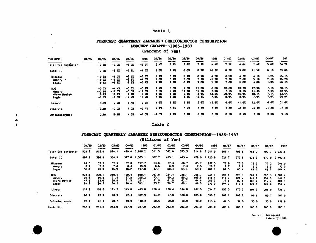
I
itk
I
Y/Q GRWTH
Total Samiconductor
ToloI IC
BIpoIar Memory Logic
HOS Umory Micro Qmr-tta Logic
Linaor
Ditcrata
Opt««iectr9nl:c
Table 1
FORECAST gilARTERLY JAPANESE SQlIOOHDUCTOR CONSUMPTION PERCENT GROWTH—1985-1987
(Percent o f Yen)
01/85 02/85 03/85 04/85
-2.CT
-2.7X
-»e.5% -ie.3% -le.GC
-3.755 -12.8X
ie .9X -i.m
3.9X
-3.9X
2.a(
-2.2X
-3.ex
-8.33S -ie.3X -fl.m
-4.4X -17.7X ie.9X -e.ix
2.2X
-2.2%
le.ex
-e.9X
-2.ex
-e.6x
-B.6X e.Tx
-5.2X -5.5X 4.6X
-12.2X
3. IX
1.7X
4.5X
1985
-2.3X
-1.5X
-3.ax -4.5X -3.7X
-3.2X -19.5X 2.2X 17.2X
2.9X
-5.7X
-1.3X
01/86 Q2/B6 03/86 04/86
2.4X
2.ex
1.9X 1.6X 1.9X
4.2X 8 3X e.ex 4.ex
i.ex
1.9X
-1.3X
e.ex
7. IX
6.9X 6.2X 7.ex
6.SX 9.7X e.ex 8.9X
8.ex
3.ex
i.ex
S.8X
6.ax
5.9X 5.ax 6.ex
7.5X 11.3X 2.ex e.ex
e.ex
3. IX
e.ex
7.2X
8.2X
8.2X 2.7X
9.ex
12.ex 18.3X 3.ex 12.IX
2.ex
5.ex
e.ex
1986
9.4X
ie.3X
4.2X -5.7X 5.7X
8.8X 7.ex 13.2X 7.5X
15.ax
6.2X
8.3X
01/87 02/87 03/87 04/87
7 5X
8.7X
6.5X 2.7X 7.ex
ie 8X 7.7X
2e.ex e.ex
e.ex
2 ex
e.ex
6.BX
9.8X
4.7X 2.6X
5.ex
ie.3x
9.2X 15.ex 8.ex 11.ex
-6.IX
e.9x
7.9r.
11.5X
4.IX 5.IX 4.ex
12.9X 14.4X 18. IX
7.ex
12.ex
-9.9X
1.2X
5 ex
6.IX
1.2X 2 4X I.ex
7. IX 7.2X 7. IX 7.ex
6 ex
-I.ex
e.ex
1987
36. 7X
39.6X
25. IX 15 2X 26.4X
48. tX 52 9X 53.6X 38 9X
31 6X
-2. IX
9.6X
Table 2
Totol Semiconductor
Total IC
Bipolar Memory Logic
MOS ttomory Micro Device Logic
Linear
Discrete
Optoelectronic
Cxct). Rt.
FORECAST QOARTERLY JAPANESE SQIIOONDUCTOR CONSQMPTION—1985-1987
(Billions o£ Yen)
04/85 1985 01/86 02/86 03/86 01/85
529.3
407.2
64.5 8.7 55.8
228.5 99.5 47.8 81.2
114.2
96.7
25.4
257. e
02/85
515.4
396.4
57.7 7.8
49.9
22e.1 86.8 53.e 8e.3
118.6
92.9
26.1
251. e
03/85
504.1
384.5
52.9 7.e 45.9
2ie.4 71.4 58.8 8e.2
121.2
9e.9
28.7
243. e
04/86 1986 01/87 02/87 03/87 04/87
499.4 2.048.2
377.e 1.565.1
52.6 6.4 46.2
199.4 67.5 61.5 70.4
125.0
92.4
30.0
207.0
227.7 29.9 197.8
858.4 325.2 221.1 312.1
479.0
372.9
110.2
237.0
511.5
387.7
53.6 6.5
47.1
207.8 73.1 61.5 73.2
126.3
94.2
29.6
203.0
542.0
415.1
57.3 6.9
50.4
221.4 80.2 61.5 79.7
136.4
97.0
29.9
203.0
573.3
443.4
6e.7 7.3
53.4
238.1 89.3 62.7 86.1
144.6
leo.o
29.9
203.0
614.8 2,241.5
479.9 1.725.9
65.7 7.5
58.2
266.7 105.6 64.6 96.5
147.5
105.0
29.9
203.0
237.3 28.2
209.1
933.9 348.1 250 3 335.5
554.7
396.2
119.4
203.0
661.1
521.7
70.0 7.7
62.3
295.4 113.7 77.5 104.2
156 3
107.1
32.3
263.6
705.8
572.6
73 3 7.9
65 4
325.8 124.2 89 1 112.5
173.5
100 6
32 6
263 0
761.9
638.3
76.3 8.3 68.0
367 .7 142 .1 105.2 120.4
194 3
90 6
33 0
203 0
799.7 2
677 0 2
77 2 8 5 68.7
393.8 1 152.3 112 7 128 8
206 0
89 7
3i 0
203 e
1987
.928.6
.409.8
296.9 32.5 264.4
,382.7 532 3 384 5 465 9
738 2
387 9
130.9
203 0
Source: Dataquest February L986
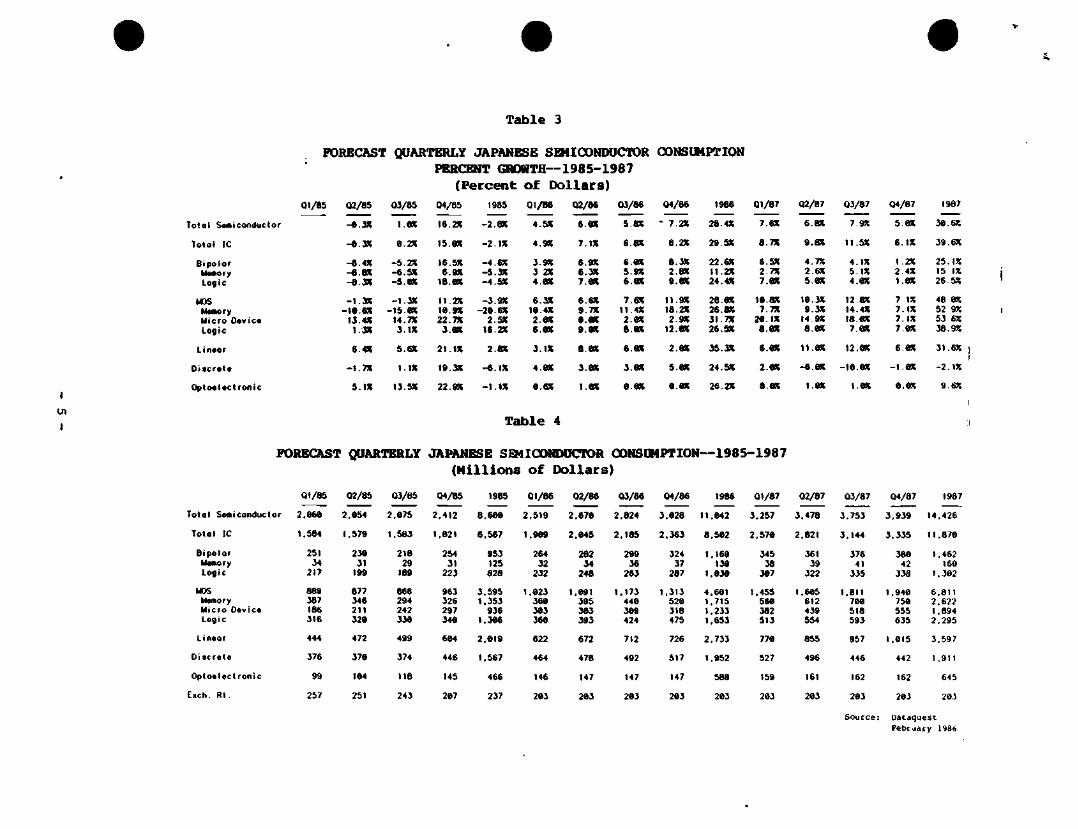
Table 3
I
ui
I
FORECAST QUARTERLY JAPANESE SBtlGDNDUCTOR OONSUMPTION PERCENT GROWTH—1985-1987
(Percent of Dollars) Ot/85 02/85
Total Semiconductor
TotoI 10
BipoIor Itonory Logic
MOS ktomory Micro Device Logic
Lineor
Diacrete
Optoelectronic
-«.3X
-e.3X
-a.4% -B.m -a.sx
-l.W -te.ex 13.4% \.3X
6.4S
-1.7X
5.IX
03/85
i.es
e.2x
-5.2X -6.5>! -S.CK
-1.3X - is .ex
14.755 3.tX
5.6X
t.ix
13.5X
04/B5
16.2X
IS.ex
16.5X 6.9X
la.M 11.2X ta.9x 22.7X 3.flK
21 .IX
19.3X
22.9X
I 985
-2.8X
-2. IX
-4.6X -5.3X -4.5X
-3.9X -28.6X
2.5X tG.2X
2.8X
- 6 . IX
-1.1X
01/86
4.5X
4.9X
3.9X 3 2X 4.ax
6.3X ia.4X 2.ex 6.ax
3. IX
4.m
e.6x
Table 4
02/86
6.ex
7. IX
6.9X 6.3X 7.ex
6.6X 9.7X a.ex e.oc
a.ex
3.ex
i.ex
03/86
5.ax
6.8X
6.ex S.9X 6.ex
7.ex 11.4X 2.ex 8.ex
6.ex
3.ex
e.ex
04/86
" 7 2X
8.2X
8.3X 2.8X e.ex
11.9X 18.2X 2.9X
12.eK
2.eK
5.ex
e.ex
1986
28.4X
29.»:
22.ec 11.2X 24.4X
28.ex 26.8X 31.7X 26.SX
35.3X
24.SX
26.2X
01/87
7.6X
8.7X
6 SX 2.7X 7.ex
le.ax 7.7X
28. IX a.ex
e.ex
2.ex
a.ex
02/87
6.ax
9.ax
4.7X 2.6X 5.ex
ie.3x 9.3X 14.9X a.ex
11.ex
-e.ex
i.ex
03/87
7 9X
11.5X
4.IX 5.IX 4.ex
12 ax 14. 4X 18.ex 7.aIi
12.ex
-le.ex
1 ex
04/87
5 ex
6.IX
1.2% 2.4X I.ex
7 IX 7. IX 7. IX 7 m
6.ax
-I.ex
e.ex
1987
3e.6X
39.6X
25. IX 15 IX 26.5X
48 er. 52 9X 53 6X 38.9X
31 6X
-2 IX
9 6X
FORECAST QOARTERLY JAPANESE SmiOONDDCTOR OONSUMPTION—1985-1987 (Millions of Dollars)
Total Semiconductor
Total IC
Bipolar Memory Logic
MOS Memory Micro Device Logic
Linear
Diacrete
Optoe Iect ronic
Exch. Rt.
01/85 02/85 03/85 04/85
2.860
1.S84
251 34 217
889 387 186 316
444
376
99
257
2.854
1.579
230 31 199
877 346 211 320
472
376
104
251
2.075
1,583
218 29 189
866 294 242 330
499
374
118
243
2.412
1.821
254 31 223
963 326 297 340
604
446
145
207
1985
8,600
6.567
953 125 828
3,595 1,353 936
1,306
2,019
1,567
466
237
01/86 02/86 03/86 04/86 1986 01/87 02/87 03/87 04/87
2,519
1,909
264 32 232
1,023 360 303 360
622
464
146
203
2,670
2,045
282 34 248
1,091 395 303 393
672
478
147
203
2,824
2.185
299 36 263
1.173 440 309 424
712
492
147
203
3,028
2.363
324 37 287
1.313 520 318 475
726
517
147
203
11,
8,
1,
1,
4, 1, I, 1,
042
502
169 139 030
,601 .715 ,233 ,653
,733
.952
588
203
3.257
2,570
345 38 307
1,455 560 382 513
770
527
159
203
3,478
2,821
361 39 322
1.605 612 439 554
855
496
161
263
3.753
3.144
376 41 335
1,811 700 518 593
957
446
162
203
Source:
3,939
3,335
380 42 338
1,940 750 555 635
1.015
442
162
203
1987
14.426
11.870
1.462 160
1.302
6.811 2.622 1.894 2.295
3.597
I .911
645
203
Dataquest Pebcjary 1986
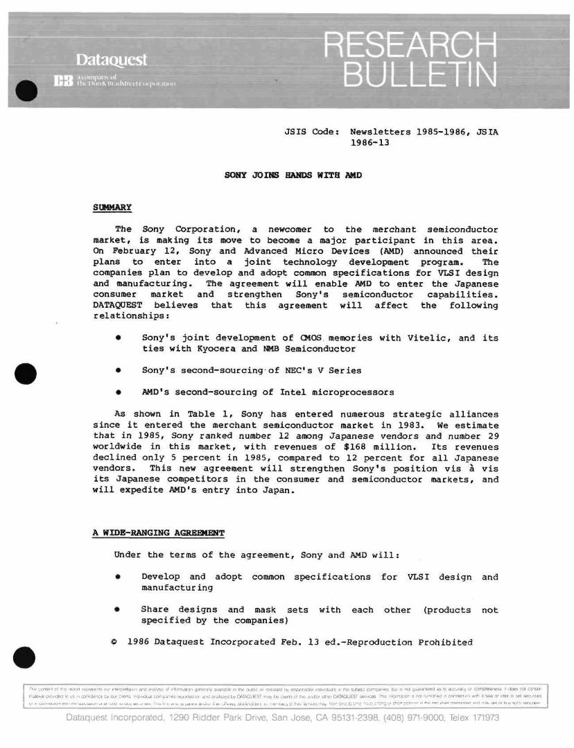
Dataqiiest RESEARCH BULLETIN
JSIS Code: Newsletters 1985-1986, JSIA 1986-13
SONY JOINS HANDS WITH AMD
SOMMARY
The Sony Corporation, a newcomer to the merchant semiconductor market, is making its move to become a major participant in this area. On February 12, Sony and Advanced Micro Devices (AMD) announced their plans to enter into a joint technology development program. The companies plan to develop and adopt common specifications for VLSI design and manufacturing. The agreement will enable AMD to enter the Japanese consumer market and strengthen Sony's semiconductor capabilities. DATAQUEST believes that this agreement will affect the following relationships:
• Sony's joint development of CMOS memories with Vitelic, and its ties with Kyocera and NMB Semiconductor
• Sony's second-sourcing of NEC's V Series
• AMD's second-sourcing of Intel microprocessors
As shown in Table 1, Sony has entered numerous strategic alliances since it entered the merchant semiconductor market in 1983. We estimate that in 1985, Sony ranked number 12 among Japanese vendors and number 29 worldwide in this market, with revenues of $168 million. Its revenues declined only 5 percent in 1985, compared to 12 percent for all Japanese vendors. This new agreement will strengthen Sony's position vis a vis its Japanese competitors in the consumer and semiconductor markets, and will expedite AMD's entry into Japan.
A WIDE-RANGING AGREBtENT
Under the terms of the agreement, Sony and AMD will:
• Develop and adopt common specifications for VLSI design and manufactur ing
• Share designs and mask sets with each other (products not specified by the companies)
© 1986 Dataquest Incorporated Feb. 13 ed.-Reproduction Prohibited
The conleni of this repon represenis our Interpretation and analysIs 0) mlormal ion generally awaIlable lo the pubiIc or released by responsible mdIviduals In Ihe subieci compan Ies bu l is not guaranteed as to accuracy or completeness It dIDes not ContaIn
material prov ided to us m conl idence by our clients individual compan ies reported on a n d analyzed by DATAQUEST may be clients of Ihis and/or other DATAQUEST services This mtormaiion is not furnished m connecl ion wilh a sale or offer to sell securities
ui in uuI intxjI iui i ' snr i rn;*> cr4\ or hi lu ty i rh SPTI irilip»:
Dataquest Incorporated, 1290 Ridder Park Drive, San Jose, CA 95131-2398, (408) 971-9000, Telex 171973
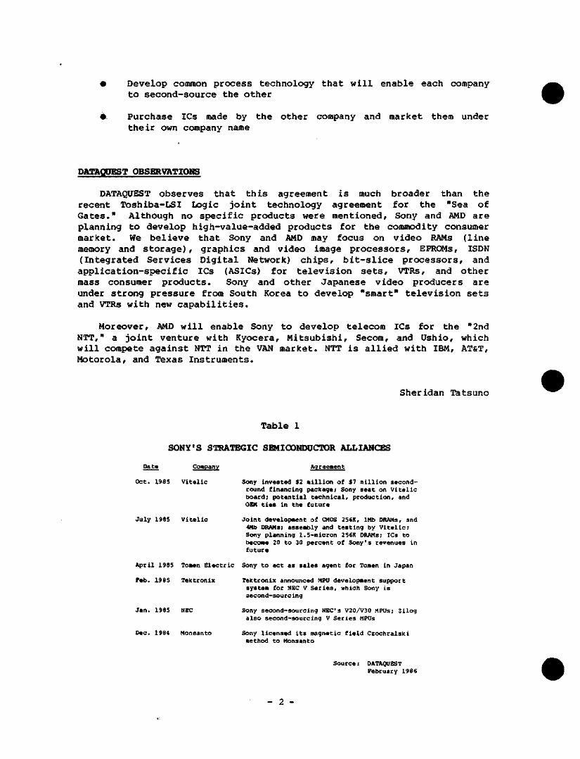
Develop common process technology that will enable each company to second-source the other
Purchase ICs made by the other company and market them under their own company name
DATAQDEST OBSERVATIOMS
DATAQUEST observes that this agreement is much broader than the recent Toshiba-LSI logic joint technology agreement for the "Sea of Gates." Although no specific products were mentioned, Sony and AMD are planning to develop high-value-added products for the commodity consumer market. We believe that Sony and AMD may focus on video RAMs (line memory and storage), graphics and video image processors, EPROMs, ISDN (Integrated Services Digital Network) chips, bit-slice processors, and application-specific ICs (ASICs) for television sets, VTRs, and other mass consumer products. Sony and other Japanese video producers are under strong pressure from South Korea to develop "smart" television sets and VTRs with new capabilities.
Moreover, AMD will enable Sony to develop telecom ICs for the "2nd NTT," a joint venture with Kyocera, Mitsubishi, Secom, and Ushio, which will compete against NTT in the VAN market. NTT is allied with IBM, AT&T, Motorola, and Texas Instruments.
Sheridan Tatsuno
Table 1
SONY'S STRATEGIC SQIICONDUCTOR ALLIANCES
Date
Oct. 1985
Company
Vitelic
Agreement
Sony invested $2 million of 37 million second-round financing pacIcage; Sony seat on Vitelic board; potential technical, production, and OEM ties in the future
Joint development of CMOS 256K, IHb ORAMs, and 4Mb ORAMs; assembly and testing by Vitelic; Sony planning 1.5-micron 2S6K DRAHs; ICs to become 20 to 30 percent of Sony's revenues in future
April 198S Tomen Electric Sony to act as sales agent for Tomen In Japan
July 1985 Vitelic
Feb. 1985 Telctronix
Jan. 1985 NEC
Dec. 1984 Monsanto
TeIctronix announced MPU development support system for NEC V Series, which Sony is second-sourc ing
Sony second-sourcing NEC's V20/V30 MPUs; Zilog also second-sourcing V Series MPUs
Sony licensed its magnetic field Czochralsl<i method to Monsanto
Source: DATAQUEST February 1986
2 -
JSIS Code : JSIA N e w s l e t t e r s 1986-5 Rev. 2 / 2 1 / 8 6
RtELIMINARy 1985 U.S.-JAPAN SailCJONDUCTOR TRADE ESTIMATES:
WINNERS AND LOSERS
SUMMARY
DATAQUEST recently completed its annual comprehensive survey of the semiconductor sales of the top 100 semiconductor companies worldwide, by region and by product. This newsletter looks at how U.S. and Japanese companies fared in each other's markets in 1985. The results: both U.S. and Japanese suppliers lost share of each other's markets, even as trade friction escalated to warlike dimensions.
U.S. companies' share of the Japanese semiconductor market declined from 11.2 percent in 1984 to 9.5 percent in 1985. Sales were off by 20 percent. Japanese companies' sales in the U.S. semiconductor market were down 37 percent; their market share fell from 15.5 percent in 1984 to 13.4 percent in 1985. In both cases, sales to the market fell substantially more than the total market fell. We will examine some reasons for this in this newsletter.
MARKET SHARE ESTIMATES
Table 1 shows estimated semiconductor sales in Japan by U.S. companies. (Note; Signetics is excluded from U.S. company sales; we now include Signetics' revenues as part of Philips-Signetics, a European-based company.) Sales peaked in 1984 at $977 million, a strong increase of 65 percent from 1983. In 1985, however, sales of MOS ICs plunged 25 percent. Also hard hit were discrete and optoelectronic devices, which fell below 1983 levels. Compound annual growth rates (CAGRs) for the four-year period shown in this table and the two following tables are skewed due to the dramatically large sales decline in 1985.
© 1986 Dataquest Incorporated Jan. 31 ed.-Reproduction Prohibited
The content of this report represents our interpretaion and analysis of information generally available to the public or released by responsible individuals in the subject companies, but is not guaranteed as to accuracy or completeness It does not contain material provided to us in conlidence by our clients Individual companies reported on and analyzed by DATAQUEST, may be clients of this and/or other DATAQUEST services Ttiis information is not furnished in connection with a saIe or offer to seII securities or in connection with the solicitation of an offer to buy securities This firm and its parent and/or their officers, stockholders, or members of their families may, from time to time, have a long or short position in the securities mentioned and may sell or buy such securities.
Azabu Heights, Suite 711, 1-5-10 Roppongi, Minato-ku, Tokyo 106, Japan 1290 Bidder Park Drive / San Jose, CA 95131 / (408) 971-9000 / Telex 171973
Semiconductor sales in the United States by Japanese companies are shown in Table 2. The Japanese companies had enjoyed incredible growth of 80 percent from 1983 to 1984, mainly in MOS ICs, and fueled largely by explosive growth in the U.S. personal computer market. In 1985, sales fell 37 percent, from $2,067 million to $1,295 million. MOS memory sales plunged 44 percent, to $747 million, which was lower than 1983's sales.
SBIIOONDUCTOR ACCOONT BALANCE
The U.S. semiconductor account balance with Japan (i.e., U.S. sales in Japan less Japanese sales in the United States) was negative $511 million in 1985, only about half of the U.S. deficit in 1984. U.S. companies have maintained a surplus for the last four years in bipolar digital logic and linear ICs, due to a dearth of Japanese competition in those areas, particularly in industrial linear, a real U.S. strength. Table 3 shows the U.S. semiconductor account balance with Japan. Figure 1 shows U.S. sales in Japan, Japanese sales in the United States, and the U.S. account balance from 1980 through 1985.
MANUFACTURERS' SALES
Japanese semiconductor sales in the United States are dominated by the top four Japanese manufacturers, Hitachi, Fujitsu, Toshiba, and NEC. All experienced severe revenue declines in 1985, especially Hitachi and NEC, which relied heavily on DRAM sales in the United States. Hitachi, number one among Japanese manufacturers in the United States for the past four years, saw its revenues sink 41 percent in 1985, from $627 million to $367 million. Table 4 shows Japanese manufacturers' semiconductor sales in the United States from 1982 through 1985.
Texas Instruments, Intel, and Motorola, the top three U.S. semiconductor manufacturers in Japan, maintained their rankings in 1985, although all three experienced slumping revenues. AMD, which had achieved 157 percent growth in Japan in 1984, declined 56 percent in 1985, from $54 million to $24 million. National Semiconductor came in fourth in Japan, with revenues of $39 million. Table 5 shows U.S. manufacturers' semiconductor sales in Japan from 1982 through 1985.
TRADE FRICTION
At DATAQUEST's April 1985 Japanese Semiconductor Industry Conference in Hakone, Japan, U.S.-Japan trade friction was a major topic among speakers and in conversation. U.S. and Japanese government speakers at the conference called for increased communication and understanding between the two countries.
- 2 -
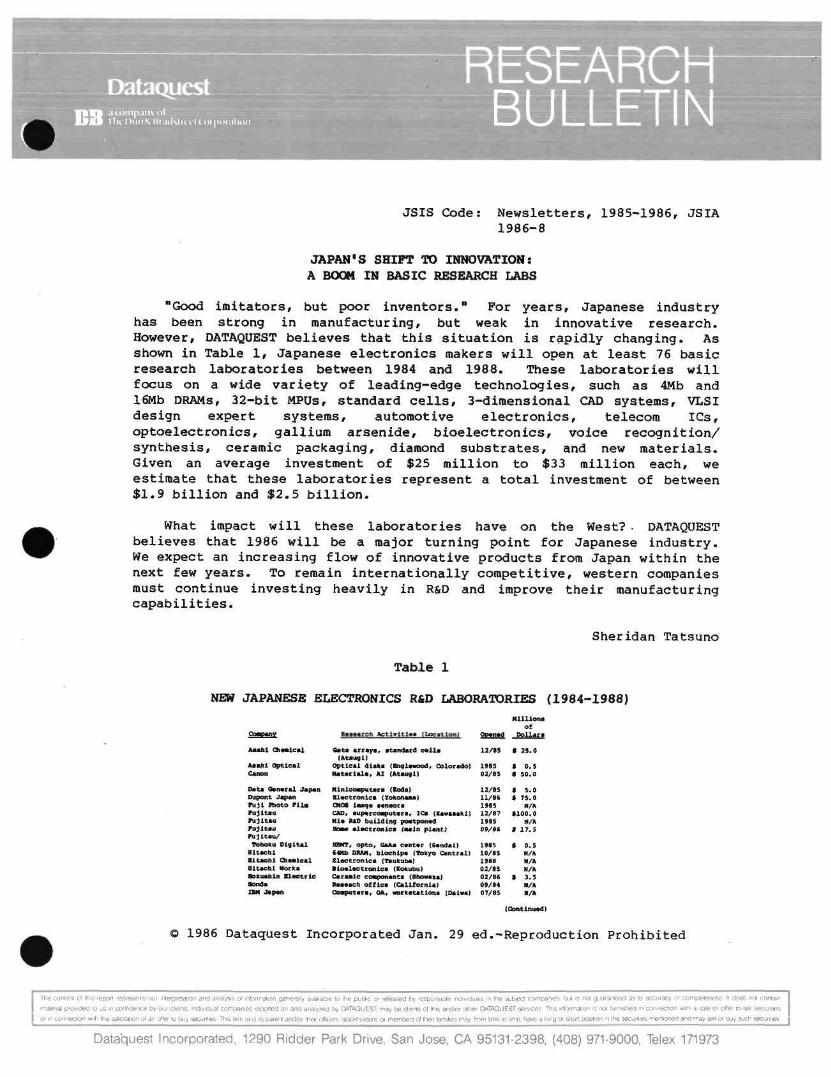
Dataquest .ui i ; i ]p. lru 111 lL i Miipih IWjiJNliti. t i iTq i
RESEARCH BULLETIN
JSIS Code: News le t t e r s , 1985-1986, JSIA 1986-8
JAPAN'S SHIFT TO INWJVATION: A BOOM IN BASIC RESEARCH LABS
"Good i m i t a t o r s , but poor i n v e n t o r s . " For y e a r s , Japanese i ndus t ry has been s t rong in manufacturing, but weak in innovat ive r e sea r ch . However, DATAQUEST b e l i e v e s t h a t t h i s s i t u a t i o n i s r ap id ly changing. As shown in Table 1, Japanese e l e c t r o n i c s makers w i l l open a t l e a s t 76 bas i c research l a b o r a t o r i e s between 1984 and 1988. These l a b o r a t o r i e s w i l l focus on a wide v a r i e t y of leading-edge t e c h n o l o g i e s , such as 4Mb and l a i b DRAMS, 32 -b i t MPUs, s tandard c e l l s , 3-dimensional CAD systems, VLSI design exper t sys tems , automotive e l e c t r o n i c s , telecom ICs, o p t o e l e c t r o n i c s , ga l l ium a r s e n i d e , b i o e l e c t r o n i c s , voice r e c o g n i t i o n / s y n t h e s i s , ceramic packaging, diamond s u b s t r a t e s , and new m a t e r i a l s . Given an average investment of $25 mi l l i on to $33 mi l l ion each, we es t ima te t h a t t hese l a b o r a t o r i e s r ep resen t a t o t a l investment of between $1.9 b i l l i o n and $2 .5 b i l l i o n .
What impact w i l l t hese l a b o r a t o r i e s have on the West? . DATAQUEST be l i eves t h a t 1986 w i l l be a major turn ing p o i n t for Japanese i n d u s t r y . We expect an inc reas ing flow of innovat ive products from Japan wi th in the next few y e a r s . To remain i n t e r n a t i o n a l l y compe t i t i ve , western companies must cont inue i nves t i ng heav i ly in R&D and improve t h e i r manufacturing c a p a b i l i t i e s .
Sheridan Tatsuno
Table 1
NEW JAPANESE ELECTRONICS R&D LABORATORIES (1984-1988)
CoKWnv
Aaahl GhaBleai
AtBhl Optical Canon
Data Ganacal Japan Dupont Japan Fuji Fhoto Flla rujitau rujltau ru^ltau Fujltau/ Tohoku Digital Hitachi aitaehl Chaalcal Hitachi Norka Bokuafain Blaetrlc Honda IBM Japan
baaacqh A^^lv^claa ItjscMtiany
Qata arraya, atandard oalla (Ataiigl)
Optical dlaka {Biglamod, Oolorado) Hatarlala, AI (Ataugl)
Hlnieoaputara (loda) Blactronlca (Yokohaaa) OIOS laaqe aanaora CAD, auparcoaputara, XCa (Kawaaakl) Hla SAD building poatponad Hoaa alactconica (sain plant)
HEHT, opto, GaAa cantar (Sandai) C « b DRAM, biochipa (Tokyo Cantral) Electronica (Taukuba) Bioalaotronlca (Kokubu) Coraaic coaponanta (Showaca) Raaaach offica (California) Coaputara, OA, aorkatationa (Oaiwa)
Opanad
12/as
19S5 02/85
12/8S 11/ee 1>85 12/87 1985 09/8«
1985 10/85 1988 02/85 02/8< 09/84 07/85
Hllllona of
Dollara
( 25.0
t o.s • 50.0
* 5.0 « 75.0
H/A $100.0
H/A $ 17.5
( 0.5 N/A N/A N/A
S 3.5 a/Ik H/A
(Oontinuad)
1986 Dataquest Incorporated Jan . 29 ed. -Reproduct ion Proh ib i ted
The conlenl ot this report represents our interpretation and analysis of information generally available to the public or released by responsible individuals m the sub|ect companies but is not guaranteed as to accuracy or corripieieness It does not contain
material provided to us m confidence by our clients Individual companies repofted on and analyzed t)y [>LTAQUEST may be cherts of this and/or other [>i,TAOUEST services This information is not furnished in connection with a sale or offer lo sell securities
or m connection with ttie sdolation ot an offer to buy securities This firm and its parent and/or their officers stockholders or members of \T\eii families may from time lo time, have a long or short position m \be secunties mentioned and may sell or txiy sucn secuniIes
Dataquest Incorporated, 1290 Ridder Park Drive, San Jose, CA 95131-2398, (408) 971-9000, Telex 171973
Table 1 (Continued)
NEW JAPANESE ELECTRONICS R&D LABORATORIES (1984-1988)
Company
Japan Automation Japan Victor (JVC) JIRA Kanto Electronics Kanto Electronics Kawasaki Steel KOD Kot>e Steel Konlshiroku Kyocera Kyowa Electric Matsushita Electric Matsushita Electric Matsushita Electric Matsushita Electronics
Matsushita Reiki Mazda Minolta Mitsubishi Electric Mitsubishi Electric Mitsubishi Electric Mitsubishi Electric Mitsubishi Electric/ Mitsubishi Kasei MITI/UPT MITI/STA MITI/Tokyo University
Hakaoichi NEC NEC NEC/HOE Physics Lab Nippon Oenso Nippon Oenso Nissan Motors NHB Semiconductors NTT/H1tach i/To3h iba NTT/KDD Oki Electric Oki Electric Ono Measuring Osaka Titanium Ricoh
Sanken Electric Sanyo Sharp Sony Sumitomo Electric Tamura Works Tafceishi Electric TDK Tokyo Electron (TEL) Tokyo Sanyo Toshiba Toshiba Toshiba Ceramics Toyo Oxygen Toyo Technica Xaesu Husen Vaskawa Electric Yazaki Industries
geaearch Jtotivlties ILocation)
CAD/CAM (Fuji) 3-micron LSIs (Yamato) Laser technology center (Chiba) Joint semiconductor RiO (Nagano) iCs, peripherals (Silicon Valley) New IC materials (Kawasaki) Switching, software (Kamifuku-Oka) Research office (North Carolina) New materials (Silicon Valley lab) Electronic materials (Vancouver, WA) New materials (Chofu) Sub-micron lS(b DRAHs (Kadoma) Biochips, thin film (Kawasaki) R&O plan (Taiwan i West Germany)
4Mb, next-generation ICs (Tokyo) Electronics (East Osaka) Electronics (Yokohama) Optoelectronics, thin films (Osaka) Optical components (Obune) Semiconductors (Research Triangle) 4Mb DRAMS, X-ray, E-besm (Itami) Original OiOS HCUs
Joint materials research Basic technology research center New joint RtD system (Tsukuba)
Bioholonics Computer (Tsukuba) Consumer electronics (California) VLSI, AI, bioelectronics (Tsukuba) 32-bit MPU, GaAs, Opto (Sagamihara) Synchrotron for lMb+ ORAHs (Tsukuba) Electronics (Aichl Prefecture) Auto electronics (Michigan) Electronics CMOS DRAMS, EBPROHs (Tateyama) 64Mb-i- DRAM synchrotron (Atsugi) Transmission think-tank 1-micron VLSI R&D center (Bachioji) CAO, OA, LAN, E-mail (Takasaki) Sensors, measuring (Yokohama) VLSI wafers (Saga) Optoelectronics, materials (Yokohama)
Semiconductors (Saitama) Bioelectronics, AI, FA (Tsukuba) 0.8- to 1.2-micron VLSI, (Fukuyama) Optical media (Portland, Oregon) IC materials (Raleigh, N. Carolina) Semiconductors (Tokyo) Telecommunications (Machida) Components (Ichikawa) Ultra LSI equipment (Nirasaki) Semiconductors 4 and 16Mb DRAMs (Kawasaki) ASICs, LANs, CAD (Horikawa) 16Mb ceramic substrates IC gas equipment (Kawasaki) CAO software (Atsugi) Satellites, wireless (California) Robots, factory automation (Okura) Hybrid ICs (Shizuoka)
Opened
03/85 04/85 1985 1985 1984 03/85 02/88 09/84 03/85 1985 09/85 10/85 04/86 1986
09/85 07/85 1986 11/84 08/85 1984 12/85 1965
11/85 1986 1985
1985 09/84 06/87 1985 01/85 08/89 1986 10/85 1985 1988 1985 1985 11/85 10/89 09/85
04/86 1985 10/85 09/85 1984 1984 02/85 03/86 N/A
12/85 02/86 04/85 01/87 1985 1986 12/84 1985 04/86 06/85
Millions of
Dollars
$
$
$
S S $
15.0 N/A 1.0 N/A N/A N/A 25.0 N/A 0.3
10.0 5.0
$100.0
$
s $
$ «
$
$ $
$
3.0 N/A
80.0 10.0 N/A 15.0 15.0 N/A 90.0 N/A
1.5 56.0 N/A
N/A N/A 65.0
$100.0
$
$ $ $ $ $ s $
N/A N/A N/A 8.0 N/A 30.0 0.8 46.5 25.0 25.0 10.0
50.0 3116.0
$
$
s »
38.5 N/A N/A N/A N/A 15.0 N/A 8.0 15.0
$110.0 $100.0
$ $ $
$
11.6 10.0 7.4 N/A 7.5 N/A
N/A » Not Available
DATAQUEST January 1986
- 2 -
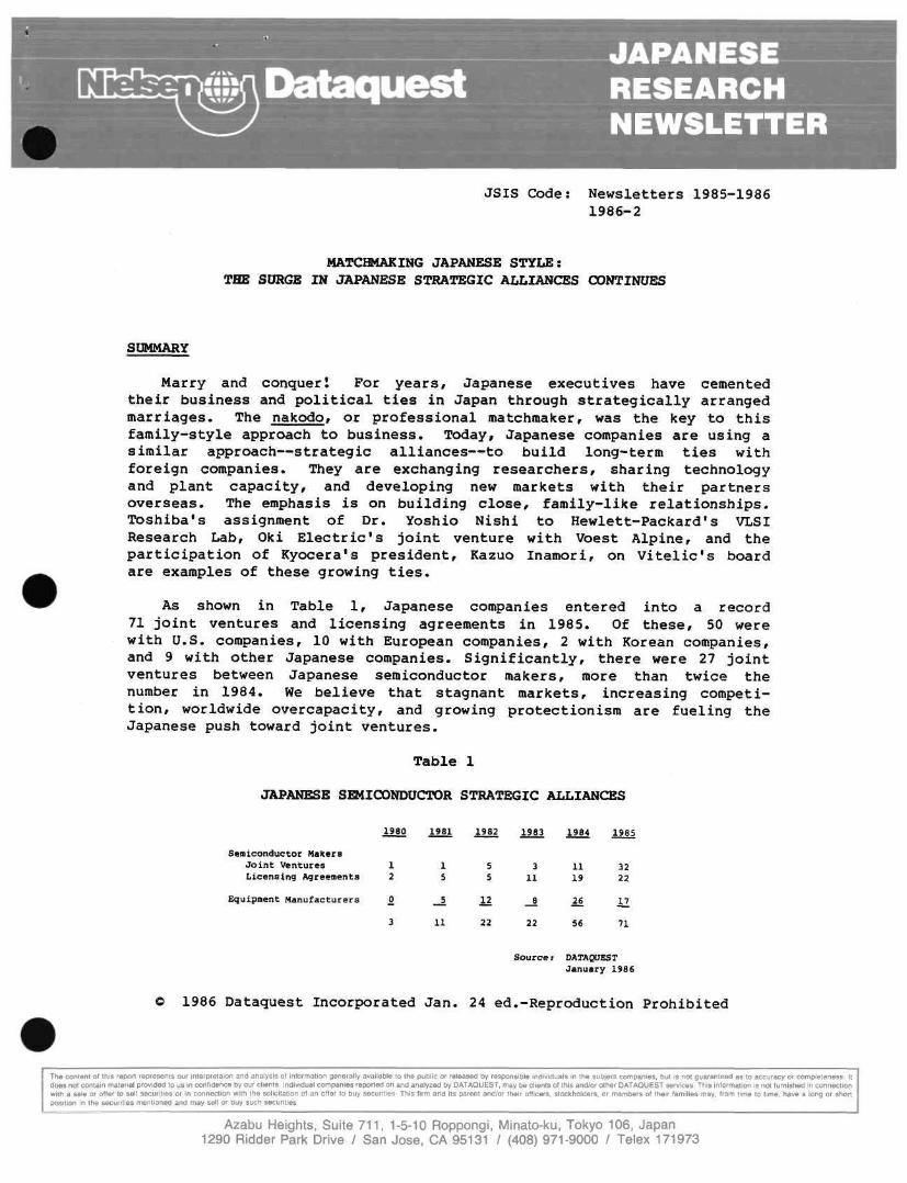
Dataquest JAPANESE RESEARCH NEWSLETTER
JSIS Code: Newsletters 1985-1986 1986-2
MATCHMAKING JAPANESE STYLE: THE SURGE IN JAPANESE STRATEGIC ALLIANCES CONTINUES
SUMMARY
Marry and conquer I For years, Japanese executives have cemented their business and political ties in Japan through strategically arranged marriages. The nakodo, or professional matchmalcer, was the key to this family-style approach to business. Today, Japanese companies are using a similar approach—strategic alliances—to build long-term ties with foreign companies. They are exchanging researchers, sharing technology and plant capacity, and developing new markets with their partners overseas. The emphasis is on building close, family-like relationships. Toshiba's assignment of Dr. Yoshio Nishi to Hewlett-Packard's VLSI Research Lab, Oki Electric's joint venture with Voest Alpine, and the participation of Kyocera's president, Kazuo Inamori, on Vitelic's board are examples of these growing ties.
As shown in Table 1, Japanese companies entered into a record 71 joint ventures and licensing agreements in 1985. Of these, 50 were with U.S. companies, 10 with European companies, 2 with Korean companies, and 9 with other Japanese companies. Significantly, there were 27 joint ventures between Japanese semiconductor makers, more than twice the number in 1984. We believe that stagnant markets, increasing competition, worldwide overcapacity, and growing protectionism are fueling the Japanese push toward joint ventures.
Table 1
JAPANESE SEMICONDUCTOR STRATEGIC ALLIANCES
1980 1981 1982 1983 1984 1985
Semiconductor Makers Joint Ventures Licensing Agreements
Equipment Hanufactuirers
1 2
0
3
1 5
_5
11
5 S
i2
22
3 11
_8
22
Source;
11 32 19 22
li 12 56 71
DATAQUEST January 1986
O 1986 Dataquest Incorporated Jan. 24 ed.-Reproduction Prohibited
The content of this report represents our interpretaion and analysis of information generally available to the public or released by responsible individuals in the subject companies, but is not guaranteed as to accuracy or completeness It does not contain material provided to us in confidence by our clients. Individual companies reported on and analyzed by DATAQUEST, may be clients of this and/or other DATAQUEST services This information is not furnished in connection with a sale or offer to sell securities or in connection with the solicitation of an offer to buy securities This firm and its parent and/or their officers, stockholders, or members of their families may, from time lo time, have a long or short position in the securities mentioned and may sell or buy such securities
Azabu Heights, Suite 711, 1-5-10 Roppongi, IVIinato-ku, Tokyo 106, Japan 1290 Bidder Park Drive / San Jose, CA 95131 / (408) 971-9000 / Telex 171973
THE SEARCH FOR IDEAL PARTNERS
In the past, Japanese strategic alliances were primarily limited to technology transfers and marketing agreements. In 1985, however, we observed a pronounced shift toward more complex and varied agreements. Japanese companies are systematically entering alliances to diversify their product portfolios, exchange technologies, penetrate markets, and utilize excess plant capacity. They are parlaying their strengths— memory technologies and CMOS wafer processing—in exchange for MPU support systems, CAD systems, and advanced IC designs. Companies like Fuji Electric, NMB Semiconductor, Oki, Ricoh, Seiko, and Sony are using their CMOS processing capabilities as a springboard into technology sharing and joint product development agreements. For many Japanese companies, the ideal partner is a company with leading-edge designs that is seeking low-cost wafer fab capacity.
Japanese semiconductor makers are also mixing their strategies. For example, Hitachi, NEC, and Toshiba are second-sourcing MPUs while jointly designing CAD systems for their proprietary MPUs with other companies. Exar, Seiko, and Sony are investing in or acquiring U.S. start-ups and offering wafer fab capacity. Some companies are simultaneously moving into several new areas. As shown in Table 2, Toshiba was the most active in 1985, signing 12 agreements covering a broad range of products.
The ground swell of strategic alliances has only begun. Because of the growing Japanese interest in Europe, and the coming shakeout in ASIC, CAD, and IC start-up companies, we believe that we will see more strategic alliances between Japanese companies in 1986. As shown in Table 3, there were 10 alliances with European companies in 1985, up from 2 in 1984.
Table 2
1985 JAPANESE STRATEGIC ALLIANCES BY COMPANY
Company
Toshiba Hitachi NEC Oki Electric Sony Mitsubishi
Number
12 7 5 6 4 3
Company
Ricoh NTT Seiko Group Matsushita Fujitsu Rohm
Number
3 3 3 2 2 2
Source: DATAQUEST January 1986
- 2 -
Table 3
1985 JAPANESE STRATEGIC ALLIANCES BY OOtJNTRY AND PRODUCT AREA
Memory Process Microprocessors ASICs Other Devices Equipment
Total
United S t a t e s
7 3
10 8 9
13
Europe
4 -2 -3 1
South Korea
----1 1
Japan
4 1 2 2
50 10
Total
11 3 16 9 15 IZ
71
Source: DATAQUEST January 1986
THE RUSH TOWARD PBODOCT GROUPINGS
We have observed that Japanese companies are forming major product groupings, or "camps," with U.S. and European makers to establish themselves worldwide. The race to find partners before being locked out of these camps is especially fierce. In 1985, we noted the following trends:
• Japanese newcomers are offering CMOS wafer fab capacity in exchange for design technology (NMB Semiconductor/Vitelic, Fuji Electric/Mosel, Seiko Epson/Xilinx/Siliconix, Rohm/Zilog, Kawasaki Steel/Nihon LSI).
• New groupings are being formed around shared product families (Sony/NMB/Vitelic, Oki/Voest/Thomson CSF/Siemens, Fuji/Mosel, Sharp/Wafer Scale Integration, Hitachi/Motorola, NEC/Sharp/ Sony/Zilog, Fujitsu/Intel).
• Japanese companies are signing up with Japanese partners, an indication of their growing confidence in domestic technology and willingness to cooperate (Kanebo/Mitsubishi, Matsushita/Hayashibara, NEC with Sharp/Oki/Sony, Casio with NEC/Oki/Hitachi, Mitsubishi/Tokyo Electron).
• Japanese-European alliances are on the rise because of Japanese interest in European markets and creative research (Oki/Thomson CSP, Toshiba/Siemens, Oki/Voest, Hitachi/Thomson CSF, Kobe Steel/Trefimetaux, Toshiba/SGS-Ates, Matsushita/Philips, Canon Sales/CIT-Alcatel).
- 3 -
• Japanese-U.S. alliances are heavily focused on microprocessor second-sourcing (10 alliances), joint ASIC development (8), and equipment joint ventures (13).
• Despite strong rivalry, Japanese-Korean ties are emerging because of cost pressures and the growing U.S.-Korean alliance (Ricoh/Hyundai, TOshiba/Pohang Jonghup Steel, Sharp/Samsung).
Overall, it appears that Japanese companies are using strategic alliances to blunt the wave of protectionism that threatens their overseas markets, an approach pioneered by Japanese automobile makers. We believe that this is the wave of the future in semiconductors. In February, we will issue a service section covering trends in Japanese strategic alliances from 1980 through 1985.
MERGERS AND ACQaiSITIOWS—THE OPENING GAMBIT?
Although Japanese companies are not noted for actively acquiring new companies, we believe that they will look at struggling U.S. start-ups as possible sources of leading-edge technology. Oki's licensing of Exel's EEPROMs and Exar's subsequent acquisition of Exel are cases in point (see Table 4) . On the other hand, U.S. equipment makers are buying out their partners to establish majority-owned Japanese subsidiaries.
Table 4
1985 JAPANESE SEMICONDUCTOR MERGERS AND ACQUISITIONS
Date Japanese
12/85 Exar (Rohm)
12/85 Midoriya
Foreign Activity
Exel Exar offer to acquire Exel; Exar to exchange $5.7 million in newly issued stock for common and preferred stock held by Exel shareholders; Exel has 5.7 million shares of stock outstanding; agreement awaiting approval of Exel shareholders
Materials MRC to buy four-fifths of Midoriya's Research 20 percent stock in 1986, bringing MRC
ownership to 98 percent
10/85 Anelva Corp. Varian
05/85 Toshiba Olivetti
Varian sold remaining 19 percent share of Anelva to NEC, which now owns Anelva completely, ending 18-year joint venture
Toshiba bought 20 percent of Olivetti Japan to become stragegic supplier to Olivetti
Sourcei DATAQUEST January 1986
- 4 -
MEMORY ALLIANCES; TRADING CMOS DRAMS FOR NEW DESIGNS
There were 11 alliances in memory technology (15 percent of all alliances) in 1985. Japanese companies were primarily interested in start-up companies like Exel, Mosel, Vitelic, and Wafer Scale Integration and in large European makers like Siemens, Thomson CSF, and Voest. The hottest technologies were CMOS 256K and 1Mb DRAMs, EEPRCMs, and 64K SRAMs. As shown in Table 5, Oki, Toshiba, and Vitelic were the most active companies. An interesting team is being formed by Vitelic (design), NMB Semiconductor (automated CMOS wafer fab), Sony (investor in Vitelic and potential OEM), and Taiwan's Electronic Research and Service Organization (Vitelic's other wafer supplier).
Table 5
1985 JAPANESE MEMORY STRATEGIC ALLIANCES
Date Japanese Foreign Agreement
11/85 NMB Semi- Vitelic Vitelic to license CMOS 1Mb DRAM conductor technology for one-third NMB plant
capacity; NMB licensing 64K SRAM from another U.S. firm; NMB Class 1 fab to ramp up to 4 million chips monthly by late 1986
10/85 Sony Vitelic Sony invested $2 million of $7 million second-round financing package; Sony seat on board; potential technical, production, and OEM ties in future
10/85 Fuji Electric
Mosel Fuji to produce CMOS 64K SRAMs for Mosel under OEM contract using Mosel's 1.5- to 2.0-micron CMOS process; Fuji to also develop custom CMOS LSIs; $74 million Fuji semiconductor investment in 1985 for plant and technology
10/85 Sharp Wafer Scale Integration
Expansion of 1984 agreement; WSI's 1.6-micron CMOS technology offered for royalties and plant capacity
09/85 Oki Thomson CSF Oki to supply 64K and 256K DRAM technology to Thomson's Marseille plant
(Continued)
- 5 -
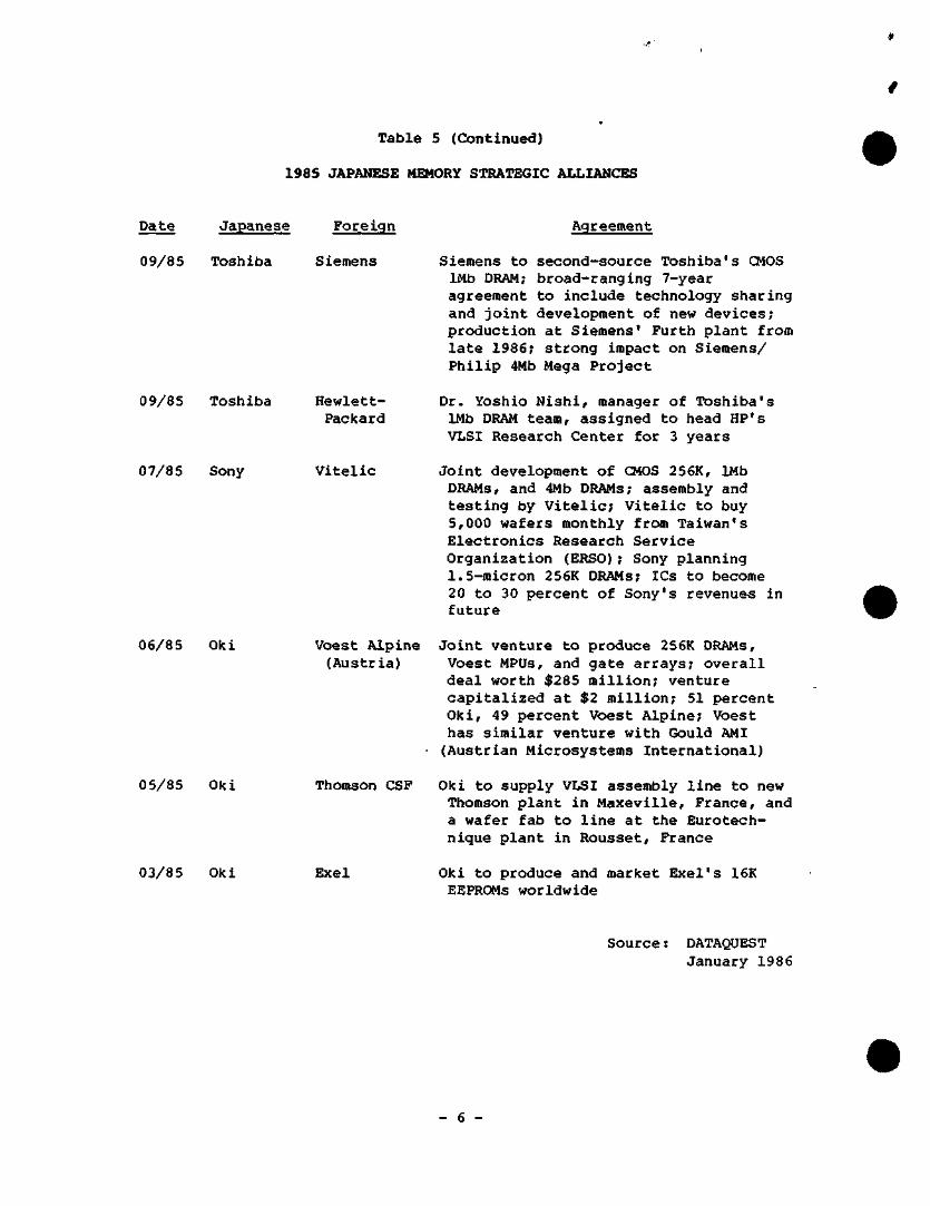
Table 5 (Continued)
1985 JAPANESE MEMORY STRATEGIC ALLIANCES
Date Japanese Foreign
09/85 Toshiba Siemens
09/85 Toshiba
07/85 Sony
Hewlett-Packard
Vitelic
06/85 Oki Voest Alpine (Austria)
05/85 Oki Thomson CSP
03/85 Oki Exel
Agreement
Siemens to second-source Toshiba's CMOS 1Mb DRAM; broad-ranging 7-year agreement to include technology sharing and joint development of new devices; production at Siemens' Furth plant from late 1986; strong impact on Siemens/ Philip 4Mb Mega Project
Dr. Yoshio Nishi, manager of Toshiba's 1Mb DRAM team, assigned to head HP's VLSI Research Center for 3 years
Joint development of CMOS 256K, 1Mb DRAMs, and 4Mb DRAMs; assembly and testing by Vitelic; Vitelic to buy 5,000 wafers monthly from Taiwan's Electronics Research Service Organization (ERSO); Sony planning 1.5-micron 256K DRAMs; ICs to become 20 to 30 percent of Sony's revenues in future
Joint venture to produce 256K DRAMs, Voest MPUs, and gate arrays; overall deal worth $285 million; venture capitalized at $2 million; 51 percent Oki, 49 percent Voest Alpine; Voest has similar venture with Gould AMI (Austrian Microsystems International)
Oki to supply VLSI assembly line to new Thomson plant in Maxeville, France, and a wafer fab to line at the Eurotech-nique plant in Rousset, France
Oki to produce and market Exel's 16K EEPRCMs worldwide
Source: DATAQUEST January 1986
- 6 -
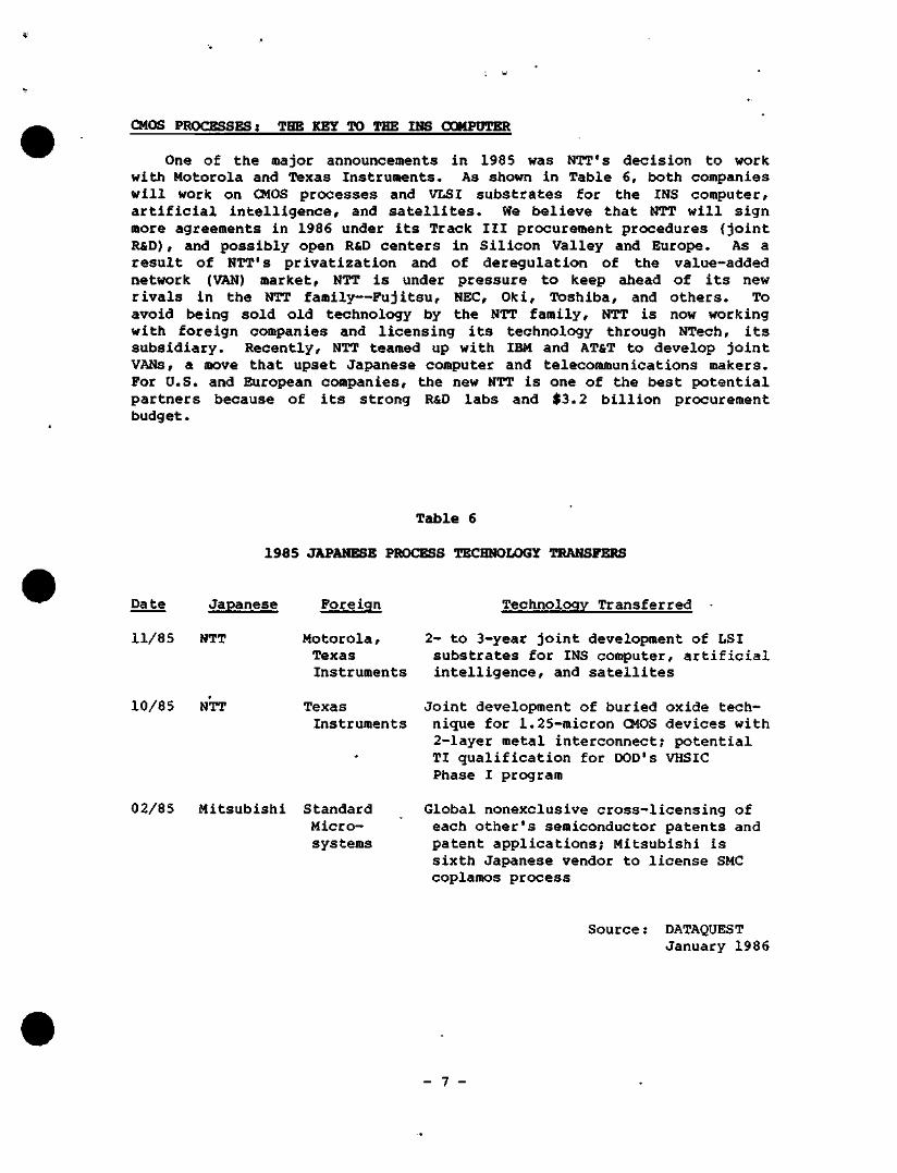
CMOS PROCESSES; THE KEY TO THE INS COMPPTER
One of the major announcements in 1985 was NTT's decision to work with Motorola and Texas Instruments. As shown in Table 6, both companies will work on CMOS processes and VLSI substrates for the INS computer, artificial intelligence, and satellites. We believe that NTT will sign more agreements in 1986 under its Track III procurement procedures (joint R&D), and possibly open R&D centers in Silicon Valley and Europe. As a result of NTT's privatization and of deregulation of the value-added network (VAN) market, NTT is under pressure to keep ahead of its new rivals in the NTT family—Fujitsu, NEC, Oki, Toshiba, and others. To avoid being sold old technology by the NTT family, NTT is now working with foreign companies and licensing its technology through NTech, its subsidiary. Recently, NTT teamed up with IBM and AT&T to develop joint VANS, a move that upset Japanese computer and telecommunications makers. For U.S. and European companies, the new NTT is one of the best potential partners because of its strong R&D labs and $3.2 billion procurement budget.
Table 6
1985 JAPANESE PROCESS TECmK>LOGy TRANSFERS
Date Japanese Foreign Technology Transferred
11/85 NTT Motorola, Texas Instruments
2- to 3-year joint development of LSI substrates for INS computer, artificial intelligence, and satellites
10/85 NTT Texas Joint development of buried oxide tech-Instruments nique for 1.25-micron OlOS devices with
2-layer metal interconnect; potential TI qualification for DOD's VHSIC Phase I program
02/85 Mitsubishi Standard Global nonexclusive cross-licensing of Micro- each other's semiconductor patents and systems patent applications; Mitsubishi is
sixth Japanese vendor to license SMC coplamos process
Source! DATAQUEST January 1986
- 7 -
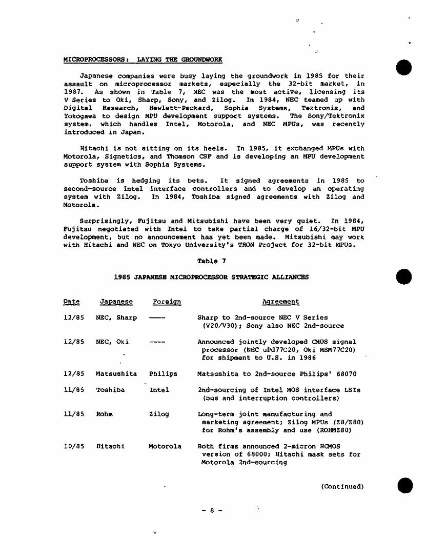
MICROPROCESSORS; LAYING THE GROUNDWORK
Japanese companies were busy laying the groundwork in 1985 for their assault on microprocessor markets, especially the 32-bit market, in 1987. As shown in Table 7, NEC was the most active, licensing its V Series to Oki, Sharp, Sony, and Zilog. In 1984, NEC teamed up with Digital Research, Hewlett-Packard, Sophia Systems, Tektronix, and Yokogawa to design MPU development support systems. The Sony/Tektronix system, which handles Intel, Motorola, and NEC MPUs, was recently introduced in Japan.
Hitachi is not sitting on its heels. In 1985, it exchanged MPUs with Motorola, Signetics, and Thomson CSF and is developing an MPU development support system with Sophia Systems.
Toshiba is hedging its bets. It signed agreements in 1985 to second-source Intel interface controllers and to develop an operating system with Zilog. In 1984, Toshiba signed agreements with Zilog and Motorola.
Surprisingly, Fujitsu and Mitsubishi have been very quiet. In 1984, Fujitsu negotiated with Intel to take partial charge of 16/32-bit MPU development, but no announcement has yet been made. Mitsubishi may work with Hitachi and NEC on Tokyo University's TRON Project for 32-bit MPUs.
Table 7
1985 JAPANESE MICROPROCESSOR STRATEGIC ALLIANCES
Date Japanese Foreign
12/85 NEC, Sharp
12/85 NEC, Oki
12/85 Matsushita Philips
11/85 Toshiba Intel
11/85 Rohm
10/85 Hitachi
Zilog
Motorola
Agreement
Sharp to 2nd-source NEC V Series (V20/V30); Sony also NEC 2nd-source
Announced jointly developed CMOS signal processor (NEC uPd77C20, Oki MSM77C20) for shipment to U.S. in 1986
Matsushita to 2nd-source Philips' 68070
2nd-sourcing of Intel MOS interface LSIs (bus and interruption controllers)
Long-term joint manufacturing and marketing agreement; Zilog MPUs (Z8/Z80) for Rohm's assembly and use (ROHMZ80)
Both firms announced 2-micron HCMOS version of 68000; Hitachi mask sets for Motorola 2nd-sourcing
(Continued)
- 8 -
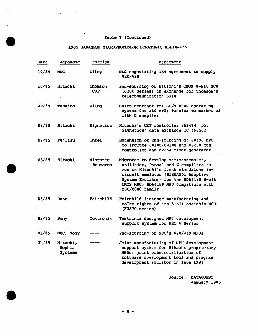
Table 7 (Continued)
1985 JAPANESE MICROPROCESSOR STRATEGIC ALLIANCES
Date
10/85
10/85
Japanese
NEC
Hitachi
Foreign
Zilog
Thomson CSF
09/85 Toshiba
09/85
09/85
Hitachi
Fujitsu
08/85 Hitachi
Zilog
Signetics
Intel
Microtec Research
03/85 Rohm
02/85 Sony
Fairchild
Tektronix
01/85
01/85
NEC, Sony
Hitachi, Sophia Systems
Agreement
NEC negotiating OEM agreement to supply V20/V30
2nd-sourcing of Hitachi's CMOS 8-bit MCU (6300 Series) in exchange for Thomson's telecommunication LSIs
Sales contract for CP/M 8000 operating system for Z80 MPU; Toshiba to market OS with C compiler
Hitachi's CRT controller (63484) for Signetics' data exchange IC (68562)
Extension of 2nd-sourcing of 80286 MPU to include 80186/80188 and 82288 bus controller and 82284 clock generator
Microtec to develop macroassembler, utilities, Pascal and C compilers to run on Hitachi's first standalone in-circuit emulator (H180AS01 Adaptive System Emulator) for the HD64180 8-bit CMOS MPU; HD64180 MPU compatible with Z80/8080 family
Fairchild licensed manufacturing and sales rights of its 8-bit one-chip MCU (F3870 series)
Tektronix designed MPU development support system for NEC V Series
2nd-sourcing of NEC's V20A30 MPUs
Joint manufacturing of MPU development support system for Hitachi proprietary MPUs; joint commercialization of software development tool and program development emulator in late 1985
Source: DATAQUEST January 1986
- 9 -
ASICS; THE BATTLELINES ARE FORMING
Japanese companies signed nine agreements for application-specific ICs (ASICs) in 1985, as shown in Table 8. Kawasaki Steel, LSI Logic, and Toshiba were clearly the most aggressive. LSI Logic and Toshiba renewed their ties to develop 50,000- to 60,000-gate "Sea of Gates" technology; Kawasaki Steel and Nihon LSI Logic are building a new CMOS plant. In 1984, Kawasaki Steel acquired silicon producer NEK Corporation, of Santa Clara, to obtain wafer processing know-how. The big question is whether LSI Logic will build its ties with Hewlett-Packard through Toshiba's Dr. Nishi.
The Seiko Group and Casio are quietly building ties of their own. Seiko Epson signed agreements with Xilinx and Siliconix, and Suwa Seikosha has ties with start-ups Applied Micro Circuits (AMCC) and SMOS System. Casio, which uses ASICs for its own products, will have Hitachi, NEC, and Oki produce its custom LSIs.
As a result of numerous joint ventures and licensing agreements, six major ASIC camps are forming. As shown in Table 9, these camps include LSI Logic, TI/Fujitsu, Fairchild/VLSI Technology, Gould/AMI, Motorola/ National, and Seiko/Honeywell. Not all companies in each camp are related, but they often share mutual ties with other companies in the group.
- 10 -
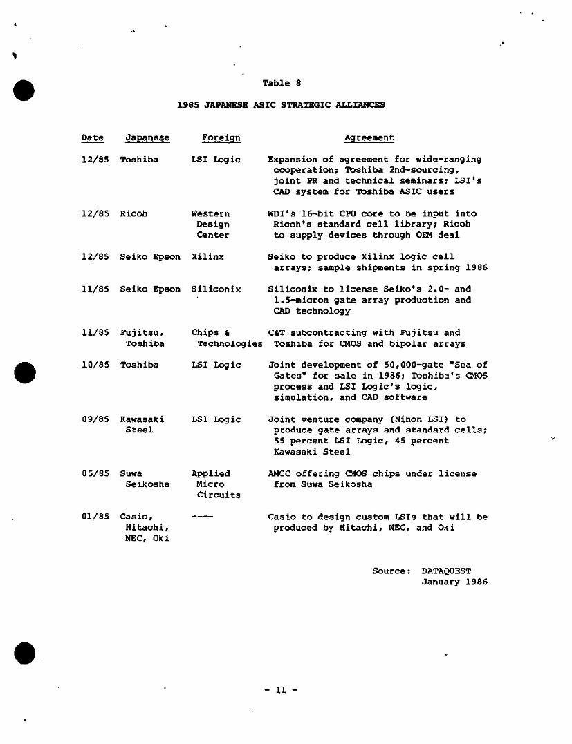
Table 8
1985 JAPANESE ASIC STRAOXGIC ALLIANCES
Date Japanese Foreign
12/85 Toshiba LSI Logic
12/85 Ricoh Western Design Center
12/85 Seiko Epson Xilinx
11/85 Seiko Epson Siliconix
11/85 Fujitsu, Toshiba
10/85 Toshiba
09/85 Kawasaki Steel
Agreement
Expansion of agreement for wide-ranging cooperation; Toshiba 2nd-sourcing, joint PR and technical seminars; LSI's CAO system for Toshiba ASIC users
WDI's 16-bit CPU core to be input into Ricoh's standard cell library; Ricoh to supply devices through OEM deal
Seiko to produce Xilinx logic cell arrays; sample shi^ents in spring 1986
Siliconix to license Seiko's 2.0- and 1.5-micron gate array production and CAD technology
Chips & C&T subcontracting with Fujitsu and Technologies Toshiba for CMOS and bipolar arrays
LSI Logic Joint development of 50,000-gate "Sea of Gates" for sale in 1986; Toshiba's OVIOS process and LSI Logic's logic, simulation, and CAO software
LSI Logic Joint venture company (Nihon LSI) to produce gate arrays and standard cells; 55 percent LSI Logic, 45 percent Kawasaki Steel
0 5/85 Suwa Seikosha
Applied Micro Circuits
AMCC offering CMOS chips under license from Suwa Seikosha
01/85 Casio, Hitachi, NEC, Oki
Casio to design custom LSIs that will be produced by Hitachi, NEC, and Oki
Source; DATAQUEST January 1986
- 11 -
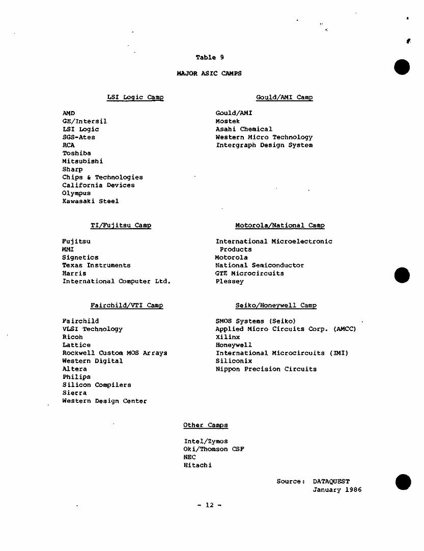
Table 9
MAJOR ASIC CAMPS
LSI Logic Camp
AMD GE/Intersil LSI Logic SGS-Ates RCA Toshiba Mitsubishi Sharp Chips & Technologies California Devices Olympus Kawasaki Steel
Gould/AMI Camp
Gould/AMI Mostek Asahi Chemical Western Micro Technology Intergraph Design System
TI/Fujitsu Camp
Fujitsu MMI Signetics Texas Instruments Harris International Computer Ltd.
Motorola/National Camp
International Microelectronic Products
Motorola National Semiconductor GTE Microcircuits Plessey
Fairchild/VTI Camp
Fairchild VLSI Technology Ricoh Lattice Rockwell Custom MOS Arrays Western Digital Altera Philips Silicon Compilers Sierra Western Design Center
Seiko/Honeywell Camp
SMOS Systems (Seiko) Applied Micro Circuits Corp. (AMCC) Xilinx Honeywell International Microcircuits (IMI) Siliconix Nippon Precision Circuits
Other Camps
Intel/Zymos Oki/Thomson CSF NEC Hitachi
Source: DATAQUEST January 1986
- 12 -
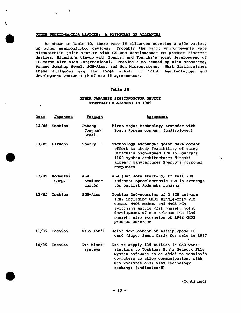
OTHER SailCONPaCTOR DEVICES; A POTPOORRI OF ALLIANCES
As shown in Table 10, there were 15 alliances covering a wide variety of other semiconductor devices. Probably the major announcements were Mitsubishi's joint venture with GE and Westinghouse to produce discrete devices, Hitachi's tie-up with Sperry, and Toshiba's joint development of IC cards with VISA International. Toshiba also teamed up with Brooktree, Pohang Jonghup Steel, SGS-Ates, and Sun Microsystems. What distinguishes these alliances are the large number of joint manufacturing and development ventures (9 of the 15 agreements).
Table 10
OTHER JAPANESE SQ4ICONDUCTOR DEVICE STRATEGIC ALLIANCES IH 1985
Date Japanese
12/85 Toshiba
Foreign
Pohang Jonghup Steel
Agreement
First major technology transfer with South Korean company (undisclosed)
11/85 Hitachi Sperry Technology exchange; joint development effort to study feasibility of using Hitachi's high-speed ICs in Sperry's 1100 system architecture; Hitachi already manufactures Sperry's personal computers
11/85
11/85
Kodenshi Corp.
Toshiba
ABM Semiconductor
SGS-Ates
ABM (San Jose start-up) to sell 200 Kodenshi optoelectronic ICs in exchange for partial Kodenshi funding
Toshiba 2nd-sourcing of 3 SGS telecom ICs, including CMOS single-chip PCM combo, NMOS modem, and NMOS PCM switching matrix (1st phase); joint development of new telecom ICs (2nd phase); also expansion of 1982 CMOS process contract
11/85 Toshiba
10/85 Toshiba
VISA Int'l
Sun Microsystems
Joint development of multipurpose IC card (Super Smart Card) for sale in 1987
Sun to supply $35 million in CAD workstations to Toshiba; Sun's Network File System software to be added to Toshiba's computers to allow communications with Sun workstations; also technology exchange (undisclosed)
(Continued)
- 13 -
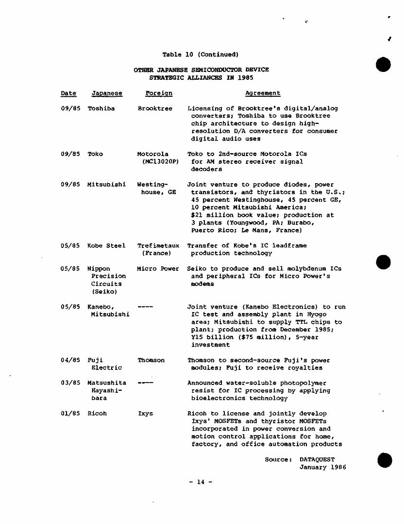
Table 10 (Continued)
OTHER JAPANESE SEMICONDUCTOR DEVICE STRATEGIC ALLIANCES IN 1985
Date Japanese
09/85 Toshiba
09/85 Toko
Foreign Agreement
Brooktree Licensing of Brooktree's digital/analog converters; Toshiba to use Brooktree chip architecture to design high-resolution D/A converters for consumer digital audio uses
Motorola Toko to 2nd-source Motorola ICs (MC13020P) for AM stereo receiver signal
decoder s
09/85 Mitsubishi Westing- Joint venture to produce diodes, power house, GE transistors, and thyristors in the U.S.;
45 percent Westinghouse, 45 percent GE, 10 percent Mitsubishi America; $21 million book value; production at 3 plants (Youngwood, PA; Burabo, Puerto Rico; Le Mans, France)
05/85 Kobe Steel Trefimetaux Transfer of Kobe's IC leadframe (France) production technology
05/85 Nippon Precision Circuits (Seiko)
05/85 Kanebo, Mitsubishi
Micro Power Seiko to produce and sell molybdenum ICs and peripheral ICs for Micro Power's modems
Joint venture (Kanebo Electronics) to run IC test and assembly plant in Hyogo area; Mitsubishi to supply TTL chips to plant; production from December 1985; Y15 billion ($75 million), 5-year investment
04/85 Fuji Thomson Electric
03/85 Matsushita Hayashi-bara
01/85 Ricoh Ixys
Thomson to second-source Fuji's power modules; Fuji to receive royalties
Announced water-soluble photopolymer resist for IC processing by applying bioelectronics technology
Ricoh to license and jointly develop Ixys' MOSFETs and thyristor MOSFETs incorporated in power conversion and motion control applications for home, factory, and office automation products
Source: DATAQUEST January 1986
- 14 -
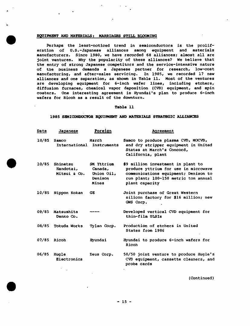
EQUIPMENT AND MATERIALS; MARRIAGES STILL BLOCMING
Perhaps the least-noticed trend in semiconductors is the proliferation of U.S.-Japanese alliances among equipment and materials manufacturers. Since 1980, we have recorded 68 alliances; almost all are joint ventures. Why the popularity of these alliances? We believe that the entry of strong Japanese competitors and the service-intensive nature of the business demands a Japanese partner for research, low-cost manufacturing, and after-sales servicing. In 1985, we recorded 17 new alliances and one separation, as shown in Table 11. Most of the ventures are developing equipment for 6-inch wafer lines, including etchers, diffusion furnaces, chemical vapor deposition (CVD) equipment, and spin coaters. One interesting agreement is Hyundai's plan to produce 6-inch wafers for Ricoh as a result of the downturn.
Table 11
1985 SmiCONOUCTOR E(^IFMENT AND MATERIALS STRATEGIC ALLIANCES
Date Japanese Foreign Agreement
10/85 Samco March International Instruments
Samco to produce plasma CVD, MOCVD, and dry stripper equipment in United States at March's Concord, California, plant
10/85 Shinetsu Handotai, Mitsui & Co.
SM Yttrium $9 million investment in plant to Canada, produce yttrium for use in microwave Union Oil, communications equipment; Denison to Denison run plant; 100-150 metric ton annual Mines plant capacity
10/85 Nippon Kokan GE Joint purchase of Great Western silicon factory for $16 million; new GWS Corp.
09/85 Matsushita Denko Co.
Developed vertical CVD equipment for thin-film ULSIs
08/85 Tokuda Works Tylan Corp. Production of etchers in United States from 1986
07/85 Ricoh Hyunda i Hyundai to produce 6-inch wafers for Ricoh
06/85 Hugle Zeus Corp. Electronics
50/50 joint venture to produce Hugle's CVD equipment, cassette cleaners, and probe cards
(Continued)
- 15 -
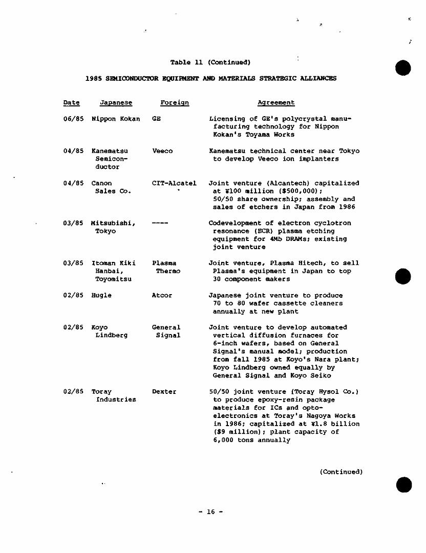
Table 11 (Continued)
1985 SEMICONDUCTOR EQUIPMENT AND MATERIALS STRATEGIC ALLIANCES
Date Japanese Foreign
06/85 Nippon Kokan GE
04/85 Kanematsu Semiconductor
Veeco
Agreement
Licensing of GE's polycrystal manufacturing technology for Nippon Kokan's Toyama Works
Kanematsu technical center near Tokyo to develop Veeco ion implanters
04/85 Canon Sales Co.
03/85 Mitsubishi, Tokyo
CIT-Alcatel
03/85
02/85
Itoman Kiki Hanbai, Toyomitsu
Hugle
Plasma Thermo
Atcor
02/85 Koyo General Lindberg Signal
02/85 Toray Dexter Industries
Joint venture (Alcantech) capitalized at ¥100 million ($500,000); 50/50 share ownership; assembly and sales of etchers in Japan from 1986
Codevelopment of electron cyclotron resonance (ECR) plasma etching equipment for 4Mb DRAMs; existing joint venture
Joint venture. Plasma Hitech, to sell Plasma's equipment in Japan to top 30 component makers
Japanese joint venture to produce 70 to 80 wafer cassette cleaners annually at new plant
Joint venture to develop automated vertical diffusion furnaces for 6-inch wafers, based on General Signal's manual model; production from fall 1985 at Koyo's Nara plant; Koyo Lindberg owned equally by General Signal and Koyo Seiko
50/50 joint venture (Toray Hysol Co.) to produce epoxy-resin package materials for ICs and optoelectronics at Toray's Nagoya Works in 1986; capitalized at ¥1.8 billion ($9 million); plant capacity of 6,000 tons annually
(Continued)
- 16 -
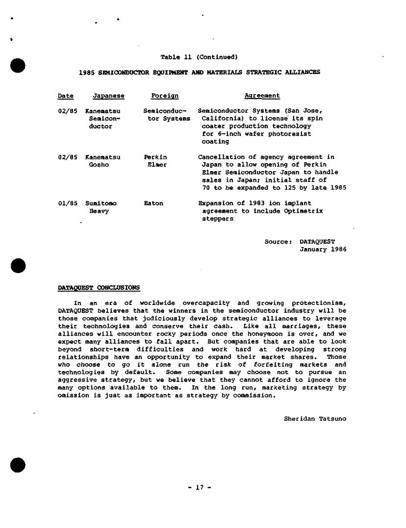
Table 11 (Continued)
1985 SEMICONDUCTOR B(^IFHENT AND MATERIALS STRATEGIC ALLIANCES
Date Japanese
02/85 Kanematsu Semiconductor
02/85 Kanematsu Gosho
Foreign
Semiconductor Systems
Perkin Elmer
01/85 Sumitomo Heavy
Eaton
Agreement
Semiconductor Systems (San Jose, California) to license its spin coater production technology for 6-inch wafer photoresist coating
Cancellation of agency agreement in Japan to allow opening of Perkin Elmer Semiconductor Japan to handle sales in Japan; initial staff of 70 to be expanded to 125 by late 1985
Expansion of 1983 ion implant agreement to include Optimetrix steppers
Source: DATAQUEST January 1986
DATAQUEST CONCLUSIONS
In an era of worldwide overcapacity and growing protectionism, DATAQUEST believes that the winners in the semiconductor industry will be those companies that judiciously develop strategic alliances to leverage their technologies and conserve their cash. Like all marriages, these alliances will encounter rocky periods once the honeymoon is over, and we expect many alliances to fall apart. But companies that are able to look beyond short-term difficulties and work hard at developing strong relationships have an opportunity to expand their market shares. Those who choose to go it alone run the risk of forfeiting markets and technologies by default. Some companies may choose not to pursue an aggressive strategy, but we believe that they cannot afford to ignore the many options available to them. In the long run, marketing strategy by omission is just as important as strategy by commission.
Sheridan Tatsuno
- 17 -
la Dataquest JAPANESE RESEARCH NEWSLETTER
JSIS Code; Newsletters 1985-1986, JSIA 1986-4
JAPANESE AND EUROPEAN SEMICONDUCTOR AGREEMENTS
Both Japan and the European community recognize the importance of promoting industrial cooperation and averting trade wars. However, over the years, friction between the European Economic Community (EEC) and Japan has increased. The main reason for this friction is the widespread view in Europe that the Japanese are penetrating European markets while restricting the flow of European goods to Japan. Japan's investment in the EEC has been high, particularly in the high-technology area. EEC investment in Japan has been much smaller, and it* has been mostly limited to traditional areas such as chemicals.
One of the ways for Japanese companies to broaden their markets in other countries is through agreements with local companies. Especially in the case of Europe, it is important for a Japanese company to be viewed as willing to cooperate locally, for political and economic reasons. For example, for a European state-controlled telecommunications authority (PTT), a Japanese product produced or developed through an agreement with an indigenous company would be viewed far more favorably for procurement than a product having no local link at all.
Thus, through alliances in Europe, the Japanese get increased market penetration. In addition, their major customers get a local supplier and the Japanese company gets access to local technology and/or products for less cost and in a shorter space of time than if a go-it-alone policy was adopted.
The benefits are not one-sided, though. The European partner gets the same advantages: an increased market penetration outside Europe, a quick and low-cost way of acquiring advanced technology and/or products, and a broader customer base.
© 1986 Dataquest Incorporated Jan. 20 ed.-Reproduction Prohibited
The content of this report represents our interpretaion and analysis Of information generally available to the public or released by responsible individuals in the subject companies, but is not guaranteed as to accuracy or completeness. It does not contain material provided to us in confidence by our clients Individual companies reported on and analyzed by DATAQUEST, may be clients of this and/or other DATAQUEST services This information is not furnished in connection with a sale or offer to sell securities or in connection with the solicitation of an offer to buy securities This firm and its parent and/or their officers, stockholders, or members ot their families may, from time to time, have a long or short position in ihs :iU(;uirii»» rnoniiOriou anCj may m l OT buj 3uC^ 39Cur;u93
Azabu Heights, Suite 711, 1-5-10 Roppongi, l\/llnato-ku, Tokyo 106, Japan 1290 Ridder Park Drive / San Jose, CA 95131 / (408) 971-9000 / Telex 171973
Table 1 lists all semiconductor agreements signed between Japanese and European companies in 1985, as well as some agreements from previous years. It is interesting to note that, apart from ICL, there is an absence of U.K. companies in the list of alliances. There seems to be a reticence on their part to get involved with Japanese companies. Two reasons could account for this situation—a general unwillingness to share their unique technologies and an unwillingness or inability to raise the necessary money to finance such alliances.
(This newsletter is reprinted with European Semiconductor Industry Service.)
the permission of DATAQUEST's
Sheridan Tatsuno Iza Hallberg
Table 1
JAPANESE-EUROPEAN SEMICONDUCTOR AGREEMENTS
Date
1985 (Nov.)
Companies
Matsushita, Philips
Agreement
Matsushita will second-source Philips' 68070 MPU. This device contains a CPU, a memory management unit, direct memory access control, an I2C bus, an RS-232-C interface, and three counters/timers—all on the same chip.
1985 (Oct.)
Hitachi, Thomson
Under this cross-licensing agreement, Thomson will second-source Hitachi's 6800 CMOS 8-bit microcontrollers. In return, Thomson will provide Hitachi with telecommunications LSI technology.
1985 Toshiba, This is a joint venture in DRAMs. Siemens (July) Siemens agreed to pay Toshiba for design, testing, and
production data on Toshiba's 1-Mbit DRAM. Siemens will thus speed up production of its megabit products. Both companies agreed on a cross-license agreement for the entire field of semiconductor component patents with mutual worldwide rights. Toshiba will gain access to Siemens' telecom technology.
1985 (May)
1985 (May)
Oki, Voest Alpine
Oki, Thomson
These companies plan a joint plant to be built in Austria to manufacture DRAMs, MPUs, and gate arrays.
Oki will supply a VLSI assembly line to the new Thomson plant in Maxeville, France, and a wafer fab line at the Eurotechnique plant in Rousset, France.
(Continued)
- 2 -
s Table 1 (Continued)
JAPANESE-EUROPEAN SEMICONDUCTOR AGREEMENTS
Date
1985 (May)
1985 (April)
1985 (Mar.)
1984
1984 (Feb.)
1984 (June)
1984 (Oct.)
Companies Agreement
Toshiba, They are taking steps toward an alliance. Olivetti Toshiba is buying 20 percent of Olivetti
Japan to become a strategic supplier to Olivetti and, therefore, to Europe.
Fuji, Thomson will second-source Fuji's power Thomson modules. Fuji gets money; Thomson gets
technology of high-power modules.
Kyocera, Philips will develop, produce, and sell Philips electronic data networks in Japan.
NMB (Minebea), NMB acquired a license to manufacture Inmos' Inmos 256K CMOS DRAM, and Inmos will buy half of
NMB's production. The two companies will also work toward a 1-Mbit chip.
Oki, Thomson
Fujitsu, ICL
Hitachi, AMI
1982 Toshiba, (Ongoing) SGS
Under an alternate source agreement, Thomson will manufacture Oki's 2- and 3-micron families of CMOS gate arrays and Oki will manufacture Thomson's 2- and 3-micron families. These products will be simultaneously marketed by both companies on a worldwide basis.
The companies extended their 1981 cooperation agreement until 1991. Fujitsu will supply gate arrays to ICL; both companies will develop new products and become committed to OSI (the computer standard).
Gould AMI and Hitachi signed an alternate-source agreement for Hitachi's family of codecs (S44230 series), with AMI (Austria Microsystems International) marketing the products in Europe.
In a continuing joint-venture agreement to develop CMOS process technology, both companies are jointly expanding CMOS logic. Manufacture will be in Italy and Japan jointly. SGS gets a modern, high-yield 3-micron CMOS process; Toshiba gets increased market penetration. The relationship will be extended to other technologies. The latest agreement is for telecom ICs.
Source; DATAQUEST January 1986
- 3 -
DataQucst .1 i l l l t l p . l l l S 111 l l l i M i n t s I V . I I I M I I 1 1 4 <ii|>i
^ESEARCK BULLETIN
JSIS Code: Newsletters 1985-1986, JSIA 1986-6
GaAs ASIC AND FOUNDRY ACTIVITIES STOR SYSTEMS DEVELOPMENT
SONPIARY
ASIC technology provides an inexpensive means of incorporating GaAs into an existing silicon subsystem or system. A user can upgrade system performance by a factor of two or three by making minor changes to existing hardware, such as incorporating GaAs into clock distribution circuits and prescalers. GaAs suppliers that support ASIC and foundry work are offering customers the opportunity to add value to existing designs, thus accelerating the transition from silicon to GaAs in very high-performance systems.
ASIC AND FOUNDRY ACTIVITIES
Application-specific GaAs devices offer a relatively attractive means of evolving system designs from the silicon world to the III-V world. Several companies have mounted substantial R&D and man«facturing programs to support GaAs ASICs, including Vitesse, TriQuint, Plessey, Honeywell, GigaBit, Adams Russell, and captive makers. Table 1 shows the fees of merchant GaAs foundries in the United States and Western Europe that were offering ASIC services in late 1985. There are no announced merchant foundries in Japan.
TriQuint and Honeywell are marketing multiuser prototype programs that allow several customers to design devices to the respective suppliers' ground rules and receive first prototype devices from wafers fabricated during a single run. To accomplish this, the vendor allots standardized reticle areas (e.g., 80 mils x 80 mils) for chip locations, such that several customers' chips can be interspersed on the same wafer. This represents a major breakthrough in economy of scale in developing new GaAs devices. The cost savings to the user can be on the order of 50 percent per wafer run.
Gene Miles Sheridan M. Tatsuno
© 1986 Dataquest Incorporated January 20 ed.-Reproduction Prohibited
The conteni of this report represents our inlerpfelation and analysis of information generally availalale to ihe pubic or released by responsible individuals in Ihe subject companies but is not guaranteed as lo accuracy or completeness ll does noi coniam
material provided lo us in confidence by Our clients Individual companies reported on and analyzed bv DATAQUEST may be clients of Ihis and/or other DAlAQUEST services This information is noi furnished m connection with a sale or offer lo sell securities
or in connection with the sdicilalion of an offer to buy securmes This firm and its parent and/or their officers siockhdders or members of their families may, from lime to lime, have a long or short posilion tn me secuniies mer^ioned ana may seii oi Duy sucn securities
Dataquest Incorporated, 1290 Ridder Park Drive, San Jose, CA 95131-2398, (408) 971-9000, Telex 171973
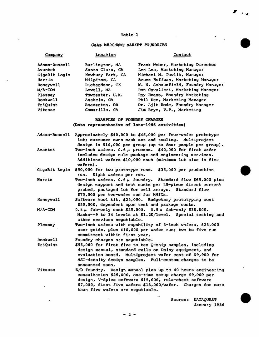
Table 1
GaAs MERCHANT MARKET FOUNDRIES
Company
Adams-Russell Avantek GigaBit Logic Harris Honeywell M/A-COM Plessey Rockwell TriQuint Vitesse
Adams-Russell
Avantek
GigaBit Logic
Harris
Honeywell
M/A-COM
Plessey
Rockwell TriQuint
Vitesse
Location
Burlington, MA Santa Clara, CA Newbury Park, CA Milpitas, CA Richardson, TX Lowell, MA Towcester, U.K. Anaheim, CA Beaverton, OR Camarillo, CA
Contact
Frank Weber, Marketing Director Len Lea, Marketing Manager Michael M. Pawlik, Manager Bruce Hoffman, Marketing Manager W. N. Schaunfield, Foundry Manager Ron Cavalieri. Marketing Manager Ray Evans, Foundry Marketing Phil Dee, Marketing Manager Dr. Ajit Rode, Foundry Manager Jim Brye, V.P., Marketing
EXAMPLES OF FOUNDRY CHARGES (Data representative of late-1985 activities)
Approximately $40,000 to $45,000 per four-wafer prototype lot; customer owns mask set and tooling. Multiproject design is $10,000 per group (up to four people per group). Two-inch wafers, 0.5 M process. $40,000 for first wafer includes design rule package and engineering services. Additional wafers $10,000 each (minimum lot size is five wafers). $50,000 for two prototype runs. $35,000 per production run. Eight wafers per run. Two-inch wafers, 0.5M foundry. Standard flow $65,000 plus design support and test costs per 25-piece direct current probed, packaged lot for cell arrays. Standard flow $75,000 per two-wafer run for MMICs. Software tool kit, $25,000. Budgetary prototyping cost $50,000, dependent upon test and package costs. 0.8 ;u fab-only cost $25,000. 0.5 M fab-only $30,000. Masks—9 to 14 levels at $1.2K/level. Special testing and other services negotiable. Two-inch wafers with capability of 3-inch wafers, £25,000 user guide, plus £10,000 per wafer run; two to five run commitment within first year. Foundry charges are negotiable. $55,000 for first five to ten Q-chip samples, including design manual, standard cells on Daisy equipment, and evaluation board. Multiproject wafer cost of $9,900 for MSI-density design samples. Full-custom charges to be announced soon. E/D foundry. Design manual plus up to 40 hours engineering consultation $25,000, one-time setup charge $9,000 per design, V-Spice software $15,000, rule-check software $7,000, first five wafers $13,000/wafer. Charges for more than five wafers are negotiable.
Source: DATAQUEST January 1986
- 2 -
Dataqiicst .1 ktLnijvinv i\\ H H n t j i i ^ U i j i k t u I M in
RESEARCH BULLETIN
JSIS Code: Newsletters 1985-1986, EIEJ 1986-7
NEC INSTITUTES TOXIC WASTE SURVEY
SUMMARY
Due to growing concern over toxic wastes, Kyushu NEC recently announced a pollution prevention agreement with Kumamoto City and has implemented a study to investigate measures for preventing toxic waste problems. The basic agreement includes the following provisions:
• Basic understanding regarding pollution prevention
Prior consultation with Kumamoto City before changes in Kyushu NEC's manufacturing processes
Urgent countermeasures
construction or
• Immediate study to investigate carcinogenic gases and chemicals
Kyushu NEC plans to issue a detailed agreement in June 1986 after investigating the matter. The agreement will cover the existing toxic waste situation, standards for individual gases and chemicals, monitoring systems, and closed water-recycling systems.
DATAQUEST ANALYSIS
DATAQUEST believes that Kyushu NEC's announcement is an indication of the serious concern over toxic wastes among Japanese semiconductor companies. Moreover, it is NEC's step to protect its plant on Kyushu island, Japan's "Silicon Island," where the company is producing 256K and 1Mb DRAMS.
During the last year, DATAQUEST has been visited by Japanese prefectural government officials who are clearly worried about toxic wastes and farmland preservation. Unlike Silicon Valley where IC plants are several miles from housing areas, most Japanese IC plants are located within several hundred yards of prime farmlands and housing areas. Given
© 1986 Dataquest Incorporated Jan. 22 ed.-Reproduction Prohibited
The conient ot Ihis report represents Our interpretation and analysis of mtormatIon generally available lo the puWIc or released by responsible IndIviduals in the subject companies bul is not guaranteed as to accuracy or completeness It ijoes not contaIn
material provided to us m confidence by our clients Individual companies reported on and analyzed by Qf TAQUEST may be clierts ot this and/or other DATAQUEST services This mformalion is not (urmshed in connection with a sale or offer to sell securities
or in connection with the sdicilalion of an otter to buy securlies This firm and its parent and/or tfieir officers siockhotders or members ot ther lamIiies may irom Dme to lIme na\e a Iong or snon poaiiun in me; bw-urmei ineiunjiic^ unu iimy acu ur lAiy aui-n aci uimcs
Dataquest Incorporated, 1290 Ridder Park Drive, San Jose, CA 95131-2398, (408) 971-9000, Telex 171973
Japan's frequent earthquakes, typhoons, and other natural disasters, toxic leaks could trigger a public outcry and seriously hamper Japanese semiconductor makers. According to the Japanese press, most prefectural governments lack toxic waste standards for high-tech industries. Japan's existing environmental regulations, a result of industrial poisoning cases in the mid-1970s, are aimed at heavy industries.
In an effort to protect the public and prevent this issue from becoming a political football, DATAQUEST believes that other Japanese semiconductor makers will also announce agreements with local governments in the future. We applaud NEC for taking the initiative in this difficult matter and believe that MITI and other semiconductor makers are closely examining the Semiconductor Industry Association (SIA) model toxic waste ordinance for possible implementation in Japan.
Sheridan Tatsuno
- 2 -
Dataquest JAPANESE RESEARCH NEWSLETTER
JSIS Code: Newsletters 1985-1986, JSIA 1986-1
JAPANESE TECHNOLOGY: THE FUTURE WAVE
At DATAQUEST's recent CAD/CAM Focus Conference in Palo Alto , JSIS Industry Analyst Sheridan Tatsuno gave a presenta t ion on Japanese semiconductor technology trends and na t iona l R&D projec ts to provide an understanding of the CAD systems required for Japan 's next-generation ICs. A copy Of h is speech, e n t i t l e d Japanese Technology; The Future Wave, i s presented on the pages tha t follow.
1986 Dataquest Incorporated Jan. 7 ed.-Reproduction Protiibited
The content of this report represents our interpretaion and analysis of information generally available to the public or released by responsible individuals m the subject companies, but is not guaranteed as to accuracy or completeness It does not contain material provided to us in confidence by our clients Individual companies reported on and analyzed by DATAQUEST, may be clients of this and/or other DATAQUEST services This information is not furnished in connection with a sale or offer to sell securities or in connection with the solicitation ol an offer to buy secunties This firm and its parent and/or their officers, stockholders, or members of their families may, from time to time, have a long or short
Azabu Heights, Suite 711, 1-5-10 Roppongi, Minato-ku, Tokyo 106, Japan 1290 Ridder Park Drive / San Jose, CA 95131 / (408) 971-9000 / Telex 171973
OVERVIEW
Leading-edge ICs
Joint R&D projects
Next-generation ICs
Next-generation computers
Market opportunities
LEADING-EDGE ICs
• Memory
• ASICs
• Microprocessors
- 2 -
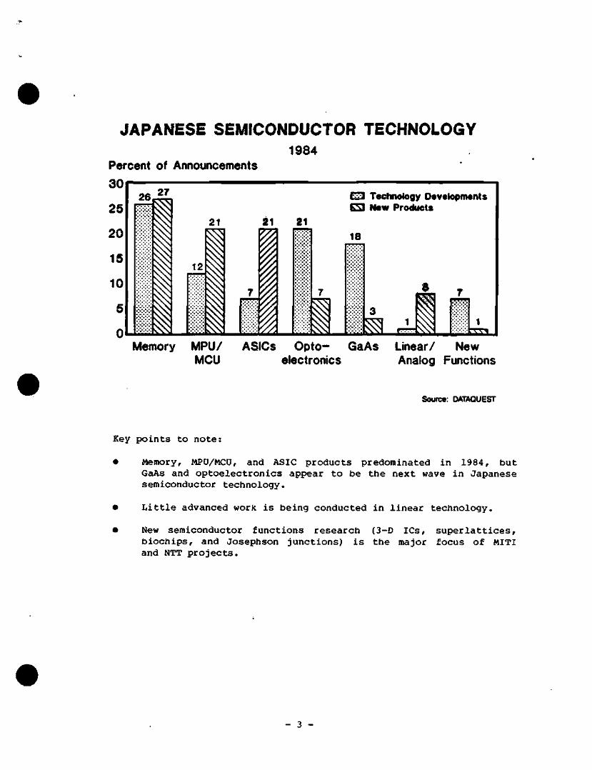
JAPANESE SEMICONDUCTOR TECHNOLOGY 1984
Percent of Announcements 30
25
20
15
10
5
27
21
•I
21 Vy
21
'I ^
C3 Technology Developments ES New Products
18
i 3 J 1 £S3.
Memory MPU/ ASICs Opto- GaAs Linear/ New MCU electronics Analog Functions
Source: DATA0UE5T
Key points to note:
• Memory, MPU/MCU, and ASIC products predominated in 1984, but GaAs and optoelectronics appear to be the next wave in Japanese semiconductor technology.
• Little advanced work is being conducted in linear technology.
• New semiconductor functions research (3-D ICs, superlattices, biochips, and Josephson junctions) is the major focus of MITI and NTT projects.
- 3 -
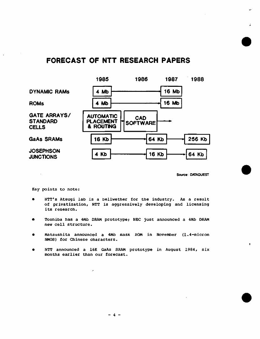
FORECAST OF NTT RESEARCH PAPERS
DYNAMIC RAMs
ROMs
GATE ARRAYS/ STANDARD CELLS
GaAs SRAMs
JOSEPHSON JUNCTIONS
1985
AUTOMATIC PLACEMENT & ROUTING
1986 1987
4 Mb
4 Mb
16 Mb
16 Mb
CAD SOFTWARE
1988
16 Kb 64 Kb 256 Kb
4 Kb 16 Kb 64 Kb
Source: DATAQUEST
Key points to note:
• NTT's Atsugi lab is a bellwether for the industry. As a result of privatization, NTT is aggressively developing and licensing its researcti.
• Toshiba has a 4Mb DRAM prototype; NEC just announced a 4Mb DRAM new cell structure.
• Matsushita announced a 4Mb mask ROM in November (1.4-raicron NMOS) for Chinese characters.
• NTT announced a 16K GaAs SRAM prototype in August 1984, six months earlier than our forecast.
- 4 -
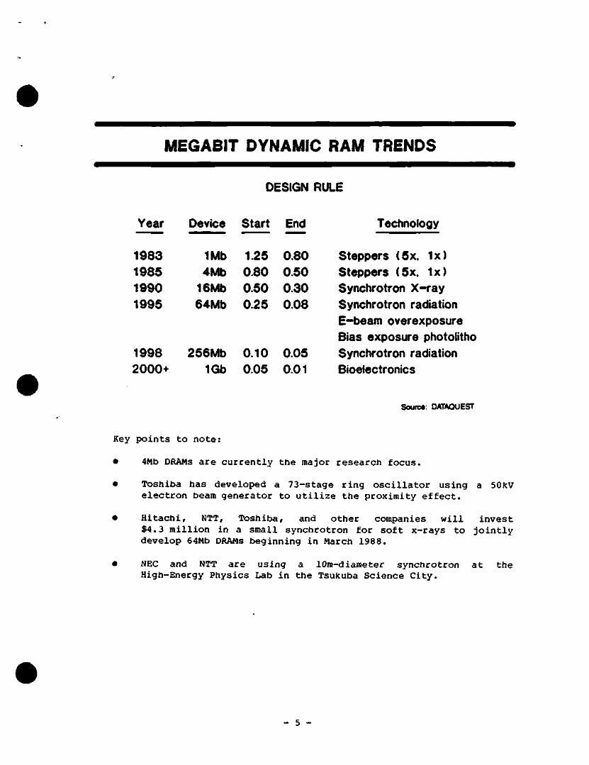
MEGABIT DYNAMIC RAM TRENDS
Year Device
1983 1Mb 1985 4Mb 1990 16Mb 1995 64Mb
1998 256Mb 2000+ 1Gb
DESIGN RULE
Start
1.25 0.80 0.50 0.26
0.10 0.05
End
0.80 0.50 0.30 0.08
0.05 0.01
Technology
Steppers (5x. 1x) Steppers (5x. 1x) Synchrotron X-ray Synchrotron radiation E-beam overexposure Bias exposure photolitho Synchrotron radiation Bioeiectronics
Source: OATAOUEST
Key points to note:
• 4Mb DRAMS are currently the major research focus.
• Toshiba has developed a 73-stage ring oscillator using a 50kV electron beam generator to utilize the proximity effect.
• Hitachi, NTT, Toshiba, and other companies will invest $4.3 million in a small synchrotron for soft x-rays to jointly develop 64Mb DRAMs beginning in March 1988.
• NEC and NTT are using a lOm-diameter synchrotron at the High-Energy Physics Lab in the Tsukuba Science City.
- 5 -
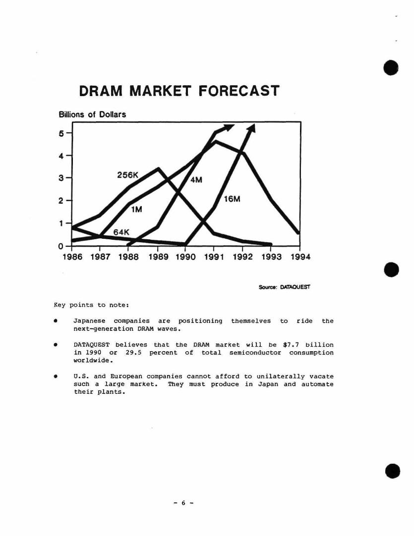
DRAM MARKET FORECAST Billions of Dollars
1986 1987 1988 1989 1990 1991 1992 1993 1994
Source: DATAQUEST
Key points to note:
Japanese companies are positioning themselves to ride the next-generation DRAM waves.
DATAQUEST believes that the DRAM market will be $7.7 billion in 1990 or 29.5 percent of total semiconductor consumption worldwide.
U.S. and European companies cannot afford to unilaterally vacate such a large market. They must produce in Japan and automate their plants.
- 6 -
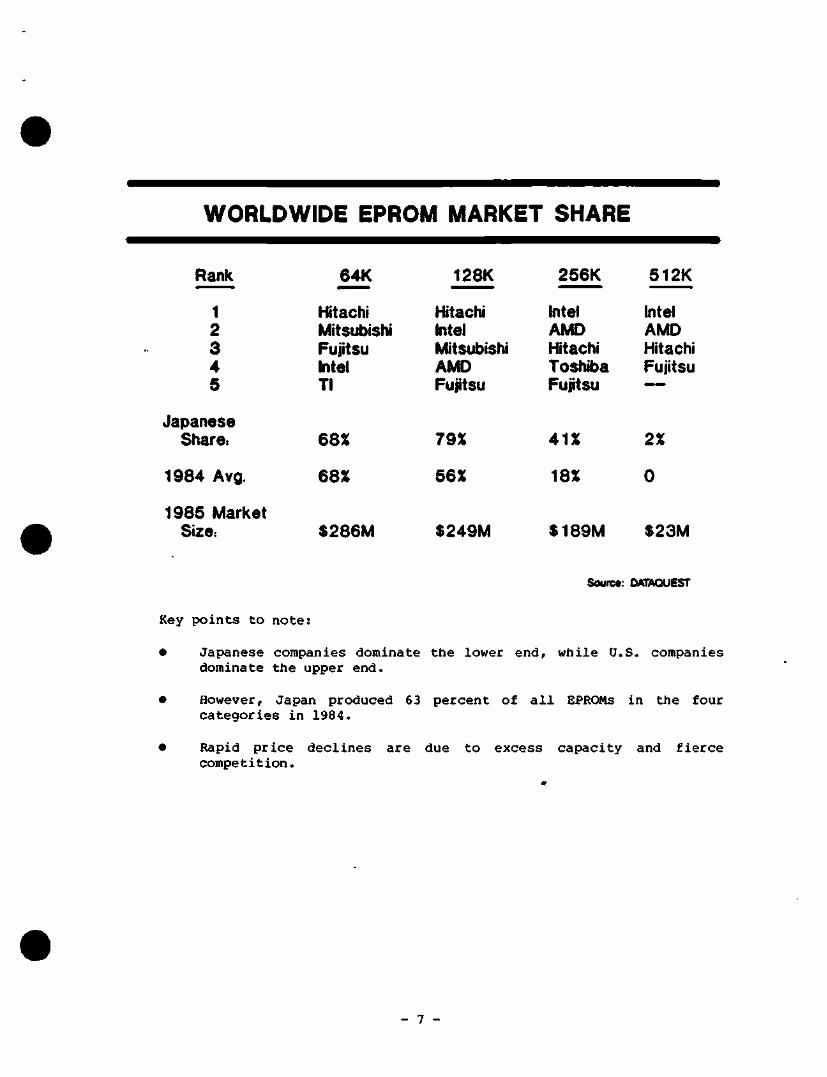
WORLDWIDE EPROM MARKET SHARE
Rank 64K 128K 256K 512K
1 2 3 4 5
Japanese Share:
1984 Avg.
1985 Market Size:
Hitachi Mitsubishi Fujitsu Intel Tl
68%
68%
$286M
Hitachi Intel Mitsubishi AMD Fujitsu
79%
56%
$249M
Intel AMD Hitachi Toshiba Fujitsu
41%
18%
$189M
Intel AMD Hitachi Fujitsu
2%
0
$23M
Source: OATAQUEST
Key points to note:
• Japanese companies dominate the lower end, while U.S. companies dominate the upper end.
• However, Japan produced 63 percent of all EPROMs in the four categories in 1984.
• Rapid price declines are due to excess capacity and fierce competition.
- 7 -
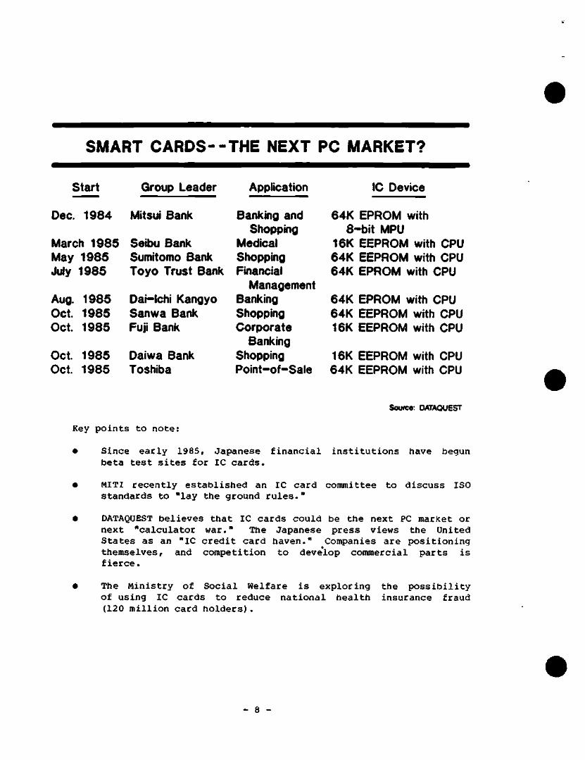
SMART CARDS--THE NEXT PC MARKET?
start Group Leader Application
Dec. 1984
March 1985 May July
Aug. Oct. Oct.
Oct. Oct.
1985 1985
1985 1985 1985
1985 1986
Mitsui Bank
Seibu Bank Sumitomo Bank Toyo Trust Bank
Dal-lchi Kangyo Sanwa Bank Fuji Bank
Oalwa Bank Toshiba
Banking and Shopping
Medical Shopping Financial
Management Banking Shopping Corporate
Banking Shopping Polnt-of-Sale
IC Device
64K EPROM with 8-blt MPU
16K EEPROM with CPU 64K EEPROM with CPU 64K EPROM with CPU
64K EPROM with CPU 64K EEPROM with CPU 16K EEPROM with CPU
16K EEPROM with CPU 64K EEPROM with CPU
Key points to note:
Source: DATAQUEST
Since early 1985, Japanese financial beta test sites for IC cards.
institutions have begun
MITI recently established an IC card committee to discuss ISO standards to "lay the ground rules."
DATAQUEST believes that IC cards could be the next PC market or next "calculator war." The Japanese press views the United States as an "IC credit card haven." Companies are positioning themselves, and competition to develop commercial parts is fierce.
The Ministry of Social Welfare is exploring the possibility of using IC cards to reduce national health insurance fraud (120 million card holders).
- 8 -
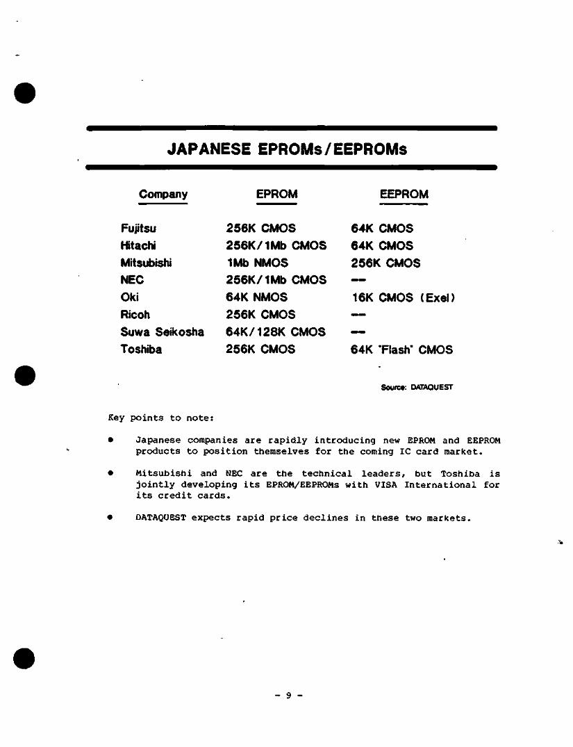
JAPANESE EPROMs/EEPROMs
Company
Fujitsu Hitachi Mitst^ishi
NEC Oki
Ricoh Suwa Seikosha Toshiba
EPROM
256K CMOS 256K/1Mb CMOS 1Mb NMOS 256K/1Mb CMOS 64K NMOS 256K CMOS 64K/128K CMOS 256K CMOS
EEPROM
64K CMOS 64K CMOS 256K CMOS —
16K CMOS (Exel) —
—
64K -Flash" CMOS
Soun»: DATAQUEST
Key points to note:
• Japanese companies are rapidly introducing new EPROM and EEPROM products to position themselves for the coming IC card market.
• Mitsubishi and NEC are the technical leaders, but Toshiba is jointly developing its EPROM/EEPROMs with VISA International for its credit cards.
• DATAQUEST expects rapid price declines in these two markets.
- 9 -
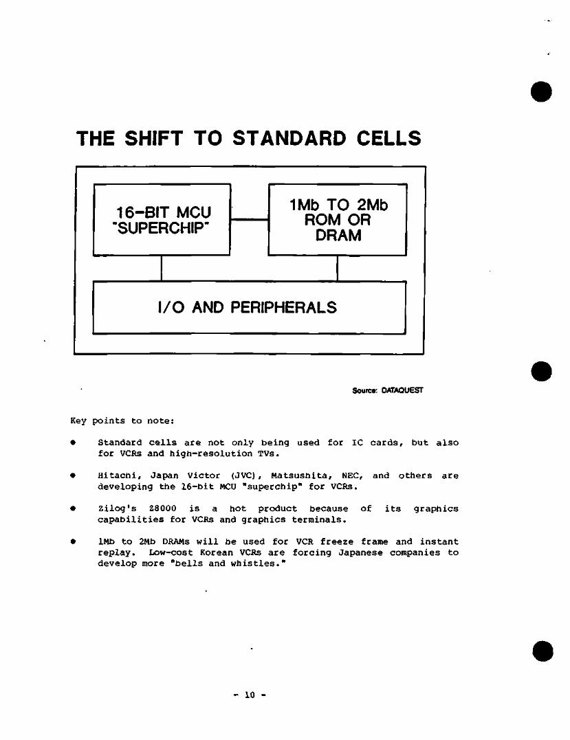
THE SHIFT TO STANDARD CELLS
16-BIT MCU "SUPERCHIP"
1Mb TO 2Mb ROM OR
DRAM
I/O AND PERIPHERALS
Source: OATAOUEST
Key points to note:
• Standard cells are not only being used for IC cards, but also for VCRs and tiigti-resolution TVs.
• Hitachi, Japan Victor (JVC), Matsushita, NEC, and others are developing the 16-bit MCU "superchip" for VCRs.
• Zilog's 28000 is a hot product because of its graphics capabilities for VCRs and graphics terminals.
• 1Mb to 2Mb DRAMs will be used for VCR freeze frame and instant replay. Low-cost Korean VCRs are forcing Japanese companies to develop more "bells and whistles."
- 10 -
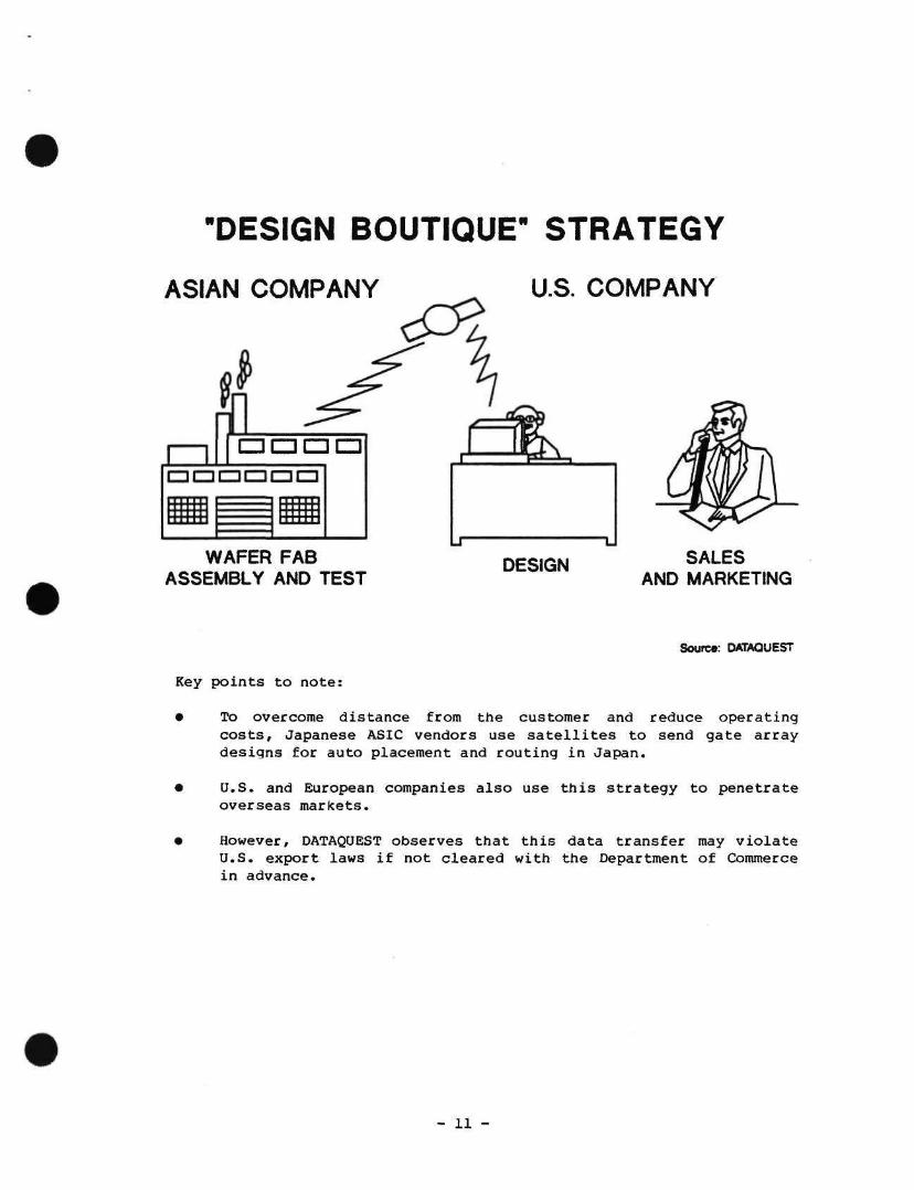
DESIGN BOUTIQUE" STRATEGY
ASIAN COMPANY
WAFER FAB ASSEMBLY AND TEST
U.S. COMPANY
DESIGN SALES AND MARKETING
Source: DATAOUEST
Key points to note:
To overcome distance from the customer and reduce operating costs, Japanese ASIC vendors use satellites to send gate array designs for auto placement and routing in Japan.
U.S. and European companies also use this strategy to penetrate overseas markets.
However, DATAQUEST observes that this data transfer may violate U.S. export laws if not cleared with the Department of Commerce in advance.
- 11 -
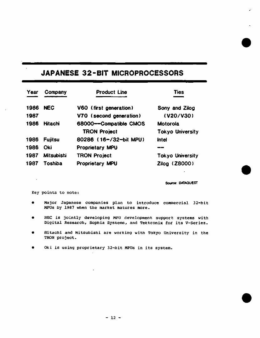
JAPANESE 32-BIT MICROPROCESSORS
Year Company Product Line Ties
1986 NEC 1987 1986 Hitachi
1986 Fujitsu 1986 Oki
1987 Mitsubishi
1987 Toshiba
V60 (first generation) V70 (second generation) 68000—Compatible CMOS
TRON Project
80286 (16- /32-b i t MPU) Proprietary MPU
TRON Project
Proprietary MPU
Sony and Zilog (V20/V30)
Motorola Tokyo University Intel
Tokyo University
Zilog (Z8000)
Source. OATAOUEST
Key points to note:
Major Japanese companies plan to introduce commercial 32-bit MPUs by 1987 when the market matures more.
NEC is jointly developing MPU development support systems with Digital Research, Sophia Systems, and Tektronix for its V-Series.
Hitachi and Mitsubishi are working with Tokyo University in the TRON project.
Oki is using proprietary 32-bit MPUs in its system.
- 12 -
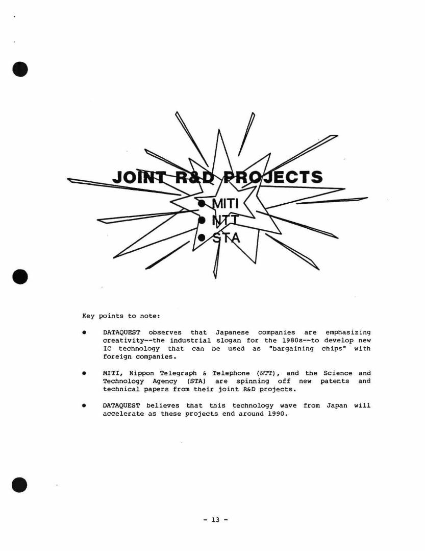
Key points to note:
• DATAQUEST observes that Japanese companies are emphasizing creativity—the industrial slogan for ttie 1980s—to develop new IC technology ttiat can be used as "bargaining chips" with foreign companies.
• MITI, Nippon Telegraph & Telephone (NTT), and the Science and Technology Agency (STA) are spinning off new patents and technical papers from their joint R&D projects.
• DATAQUEST believes that this technology wave from Japan will accelerate as these projects end around 1990.
- 13 -
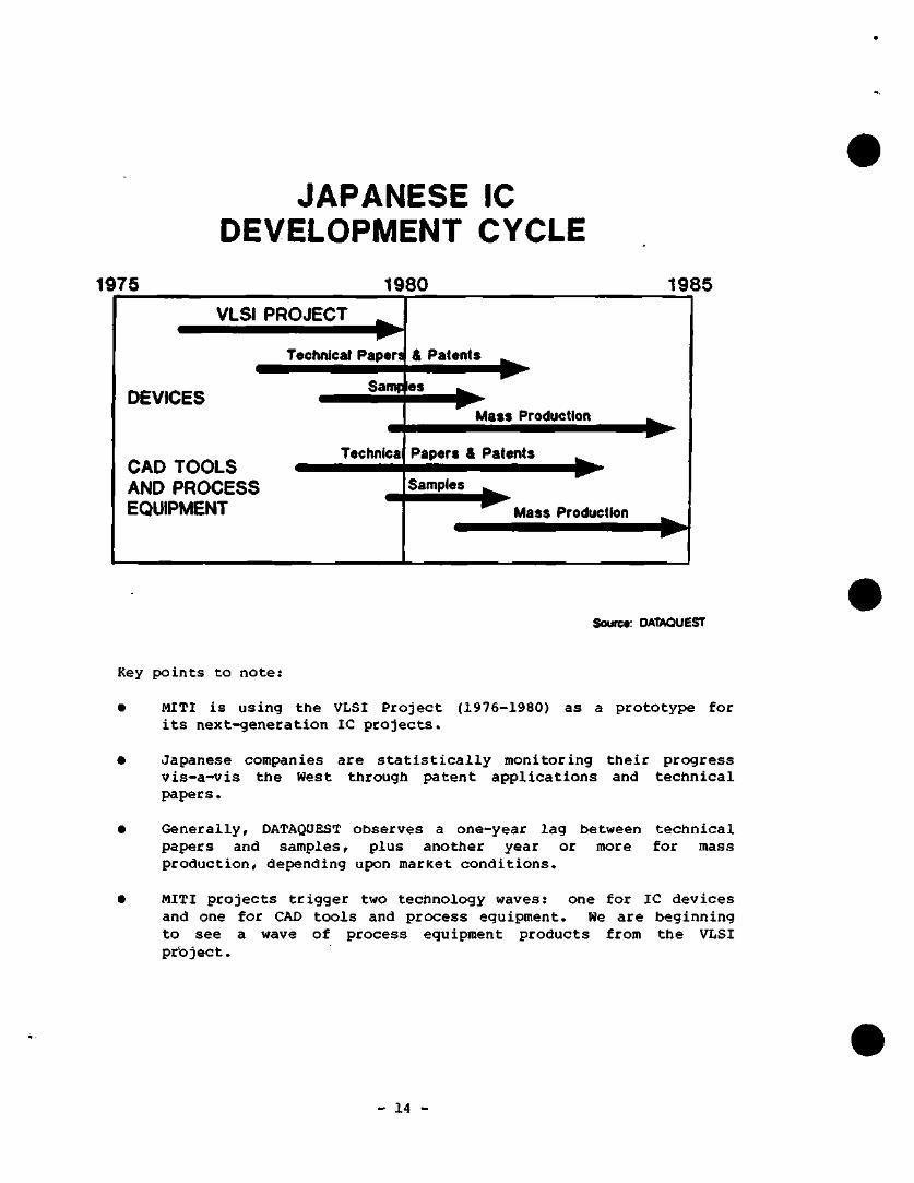
JAPANESE IC DEVELOPMENT CYCLE
1975 1980 1985
VLSI PROJECT ^
DEVICES
CAD TOOLS AND PROCESS EQUIPMENT
Technical Papers
Samp
Teehnica
& Patents ^^
les fc^
Mass Production
Papers & Patents ^
Samples ^
Mass Production
*
Source: DATAQUEST
Key points to note:
• MITI is using the VLSI Project (1976-1980) as a prototype for its next-generation IC projects.
• Japanese companies are statistically monitoring their progress vis-a-vis the West through patent applications and technical papers.
• Generally, DATAQUEST observes a one-year lag between technical papers and samples, plus another year or more for mass production, depending upon market conditions.
• MITI projects trigger two technology waves: one for IC devices and one for CAD tools and process equipment. We are beginning to see a wave of process equipment products from the VLSI prbject.
- 14 -
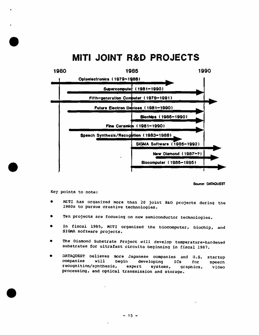
MITI JOINT R&D PROJECTS 1980 1985
Optoelectronics (1979-1968)
Supercompute (1981 -1990)
Fifth-generation Comiuter (1979-1991)
1990
Future Electron D< trices (1981-1990)
BiocNps (1986-1990)
Fine Ceramics (1981-1990)
Speech Synthesis/Recognition (1983-1988)
SIGMA Software (1985-1992)
New Diamond (1987-?)
Biocomputer (1985-1995)
Source: OATAOUEST
Key points to note:
MITI tias organized more than 20 joint R&D projects during the 1980s to pursue creative technologies.
Ten projects are focusing on new semiconductor technologies.
In fiscal 1985, MITI organized the biocomputer, biochip, and SIGMA software projects.
The Diamond Substrate Project will develop temperature-hardened substrates for ultrafast circuits beginning in fiscal 1987.
DATAQUEST believes more Japanese companies and U.S. startup companies will begin developing ICs for speech recognition/synthesis, expert systems, graphics, video processing, and optical transmission and storage.
- 15 -
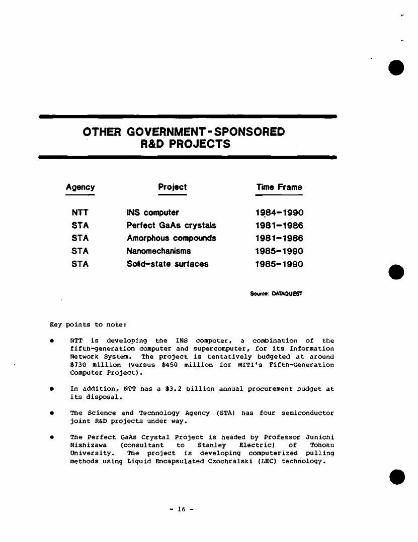
OTHER GOVERNMENT-SPONSORED R&D PROJECTS
Agency Project Time Frame
NTT
STA
STA
STA
STA
INS computer Perfect GaAs crystals Amorphous compounds
Nanomechanisms Soiid-state surfaces
1984-1990 1981-1986 1981-1986
1985-1990 1985-1990
Source: DATAOUEST
Key points to note:
• NTT is developing the INS computer, a combination of the fifth-generation computer and supercomputer, for its Information Network System. The project is tentatively budgeted at around $730 million (versus Computer Project).
$450 million for MITI's Fifth-Generation
In addition, NTT has a $3.2 billion annual procurement budget at its disposal.
The Science and Technology Agency (STA) has four semiconductor joint R&D projects under way.
The Perfect GaAs Crystal Project is headed by Professor Junichi Nishizawa (consultant to Stanley Electric) of Tohoku University. The project is developing computerized pulling methods using Liquid Encapsulated Czochralski (LEC) technology.
- 16 -
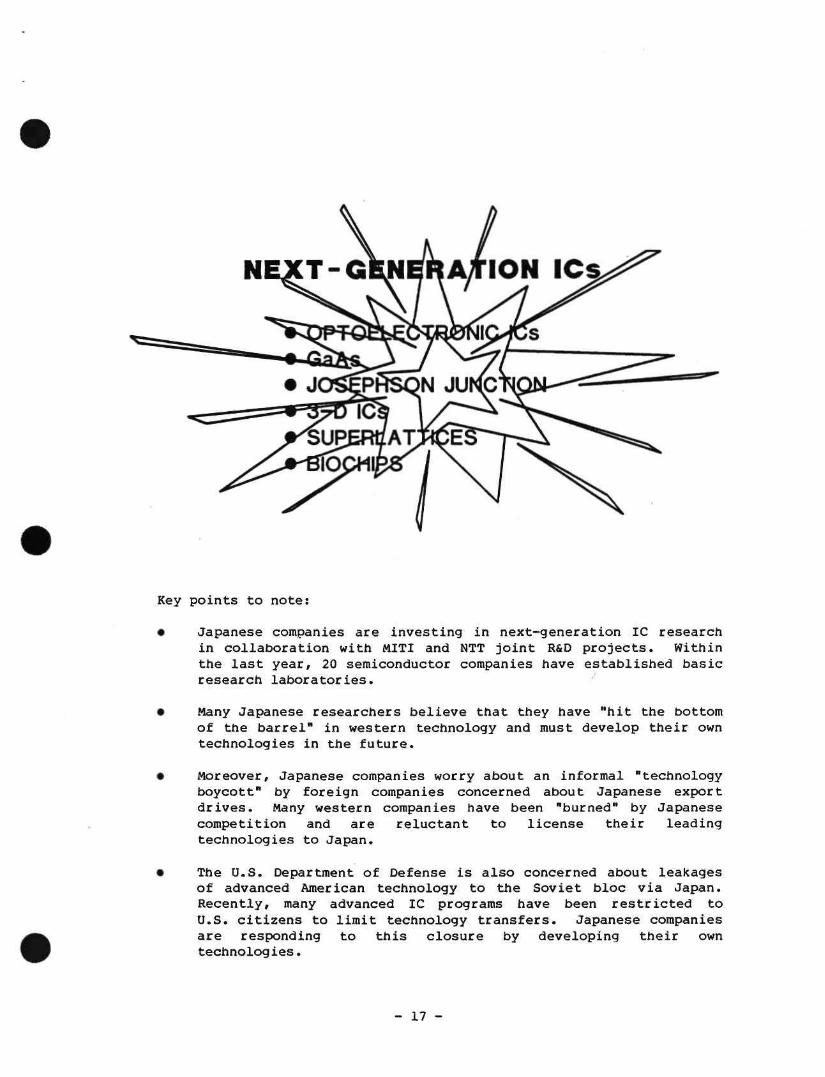
Key points to note:
• Japanese companies are investing in next-generation IC research in collaboration with MITI and NTT joint R&D projects. Within the last year, 20 semiconductor companies have established basic research laboratories.
• Many Japanese researchers believe that they have "hit the bottom of the barrel" in western technology and must develop their own technologies in the future.
• Moreover, Japanese companies worry about an informal "technology boycott" by foreign companies concerned about Japanese export drives. Many western companies have been "burned" by Japanese competition and are reluctant to license their leading technologies to Japan.
• The U.S. Department of Defense is also concerned about leakages of advanced American technology to the Soviet bloc via Japan. Recently, many advanced IC programs have been restricted to U.S. citizens to limit technology transfers. Japanese companies are responding to this closure by developing their own technologies.
- 17 -
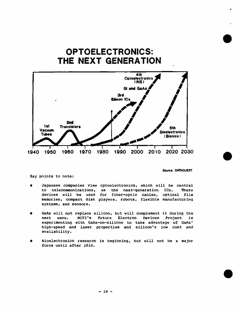
OPTOELECTRONICS: THE NEXT GENERATION
1 1940 1950
T I - I 1 r 1 r I960 1970 1980 1990 2000 2010 2020 2030
Source: DATA0UE5T
Key points to note;
Japanese companies view optoelectronics, wtiicti will be central to telecommunications, as the next-generation ICs. These devices will be used for fiber-optic cables, optical file memories, compact disk players, robots, flexible manufacturing systems, and sensors.
GaAs will not replace silicon, but will complement it during the next wave. MITI's Future Electron Devices Project is experimenting with GaAs-on-silicon to take advantage of GaAs' high-speed and laser properties and silicon's low cost and availability.
Bioelectronics researcti is beginning, but will not be a major force until after 2010.
- 18 -
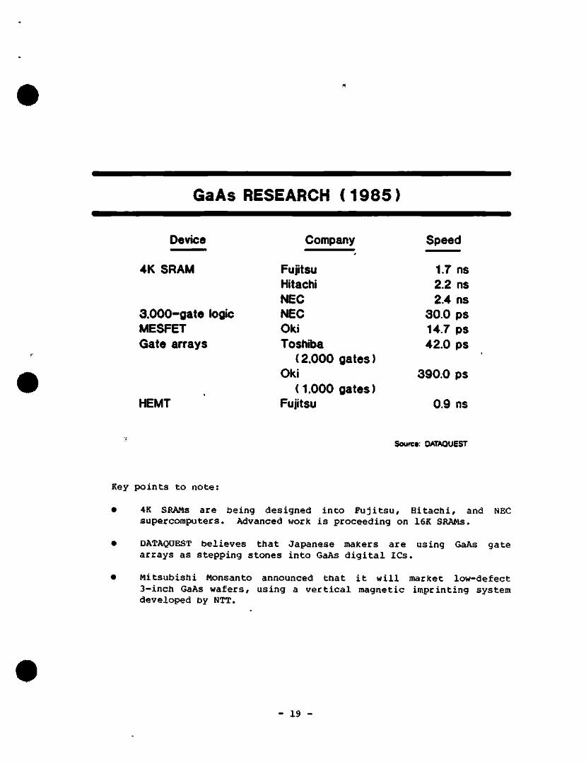
GaAs RESEARCH (1985)
Device
4K SRAM
3.000'gate logic MESFET Gate arrays
HEMT
Company
Fujitsu Hitachi NEC NEC Oki Toshiba
(2.000 gates) Oki
(1.000 gates) Fujitsu
Speed
1.7 ns 2.2 ns 2.4 ns
30.0 ps 14.7 ps 42.0 ps
390.0 ps
0.9 ns
Source: DATAOUEST
Key points to note:
• 4K SRAMs are being designed into Fujitsu, Hitachi, and NEC supercomputers. Advanced work is proceeding on 16K SRAMs.
• DATAQUEST believes that Japanese makers are using GaAs gate arrays as stepping stones into GaAs digital ICs.
• Mitsubishi Monsanto announced that it will market low-defect 3-inch GaAs wafers, using a vertical magnetic imprinting system developed by NTT.
- 19 -
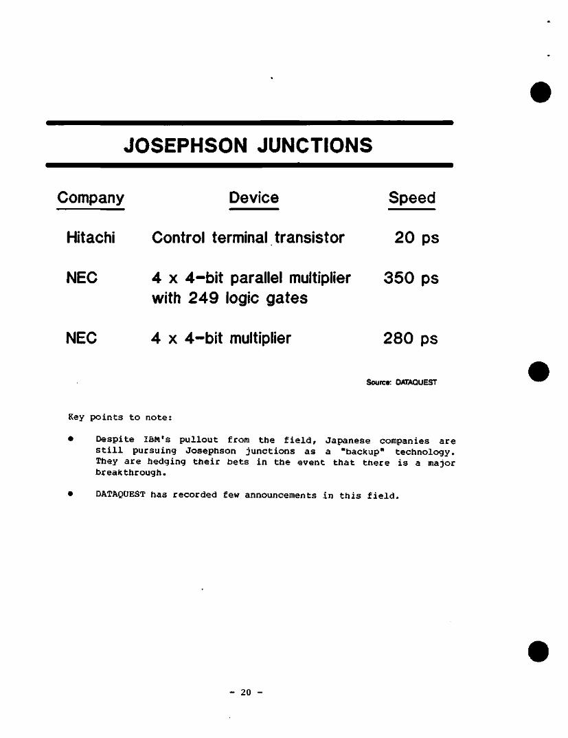
JOSEPHSON JUNCTIONS
Company Device Speed
Hitachi Control terminal transistor 20 ps
NEC 4 X 4-bit parallel multiplier with 249 logic gates
350 ps
NEC 4 X 4-bit multiplier 280 ps
Source: DATAQUEST
Key points to note:
• Despite IBM's pullout from the field, Japanese companies are still pursuing Josephson junctions as a "backup" technology. Ttiey are hedging their bets in the event that there is a major breakthrough.
• DATAQUEST has recorded few announcements in this field.
- 20 -
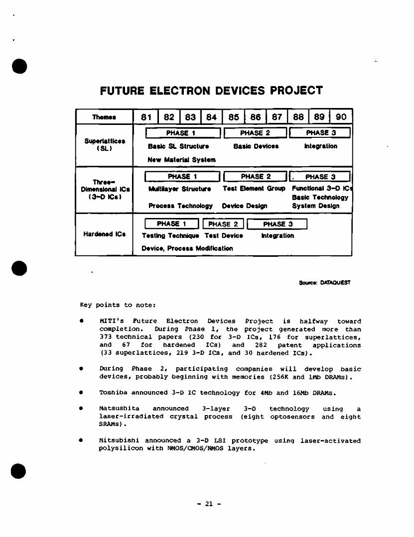
FUTURE ELECTRON DEVICES PROJECT
Themes
S(4>eriattices (SL)
Three-Dftnensionai ICs
(3 -D ICs)
Hardened ICs
81 82 83 84 85 86 87 88 89 90
1 PHASE 1 1 PHASE 2 | PHASE 3
Basic SL Structure Basic Devices Integration
New Material System
1 PHASE 1 11 P
Multilayer Structure Test B
Process Tecttnology Device
>HASE 2 I I , PHASE 3
ement Group Functional 3 - D IC: Basic Technology
Design System Design
PHASE 1 1 PHASE 2 PHASE 3
Testing Technique Test Device Integration
Device, Process Modification
Source: DAIAOUEST
Key points to note:
e MITI's Future Electron Devices Project is tialfway toward completion. During Phase 1, the project generated more than 373 technical papers (230 for 3-D ICs, 176 for superlattices, and 67 for hardened ICs) and 282 patent applications (33 superlattices, 219 3-D ICs, and 30 hardened ICs).
• During Phase 2, participating companies will develop basic devices, probably beginning with memories (256K and 1Mb DRAMs).
• Toshiba announced 3-D IC technology for 4Mb and 16Mb DRAMs.
• Matsushita announced 3-layer 3-D technology using a laser-irradiated crystal process (eight optosensors and eight SHAMS).
e Mitsubishi announced a 3-D LSI prototype using laser-activated polysilicon with NMOS/CMOS/NMOS layers.
- 21 -
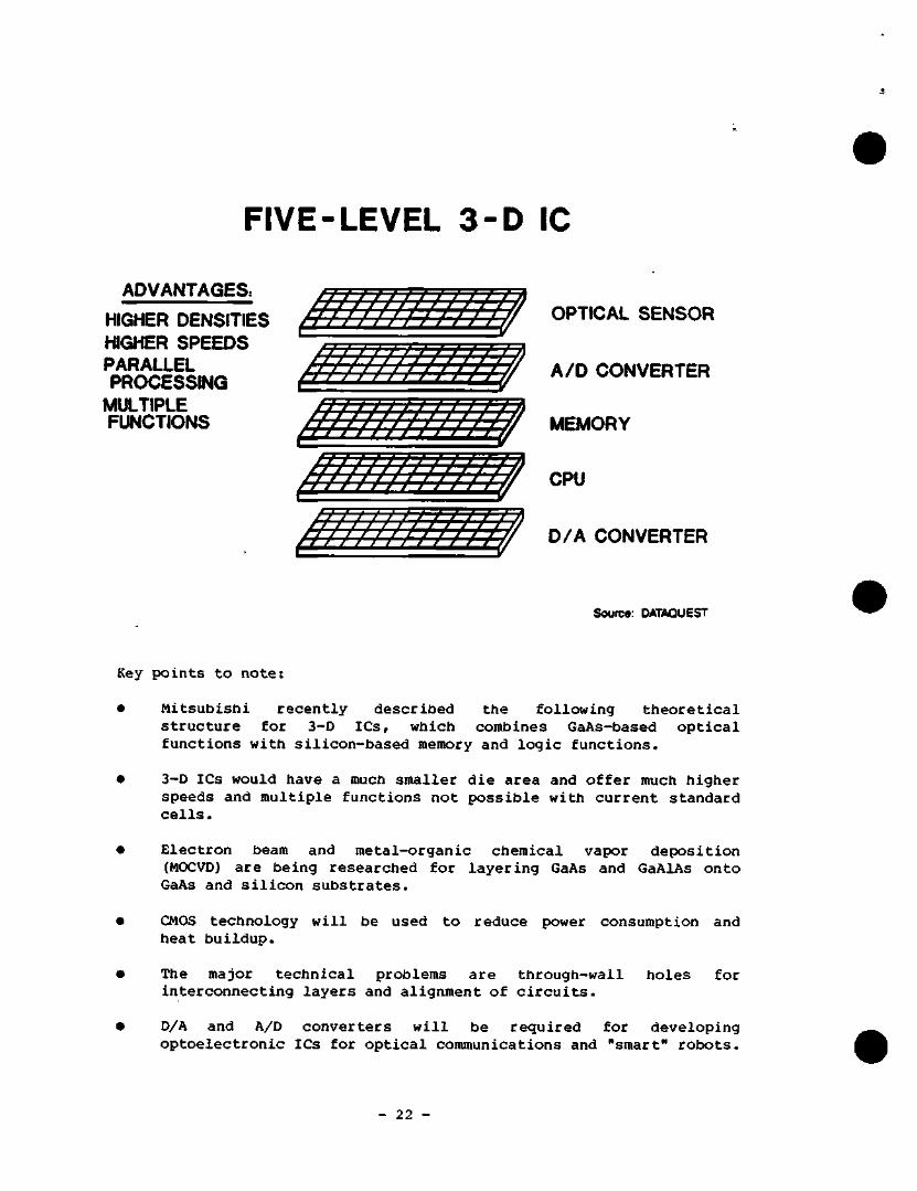
FIVE-LEVEL 3-D IC
ADVANTAGES: HIGHER DENSITIES HIGHER SPEEDS PARALLEL PROCESSING
MULTIPLE FUNCTIONS
A /D CONVERTER ^ ^ ' ^ ^ ^ ^ ^ ^ ^ ^ ^ ^ ^ ^ ^ ^ ^ ^ - ^
y>'>'<'>'<'^'>'<'.'>'<'>'^ C P U
ymmrn^
OPTICAL SENSOR
D/A CONVERTER
Sourca: DATAQUEST
Key points to note:
• Mitsubistii recently described the following theoretical structure for 3-D ICs, which combines GaAs-based optical functions witti silicon-based memory and logic functions.
• 3-D ICs would tiave a much smaller die area and offer much higher speeds and multiple functions not possible with current standard cells.
• Electron beam and metal-organic chemical vapor deposition (MOCVD) are being researched for layering GaAs and GaAlAs onto GaAs and silicon substrates.
• CMOS technology will be used to reduce power consumption and heat buildup.
• The major technical problems are through-wall holes for interconnecting layers and alignment of circuits.
• D/A and A/D converters will be required for developing optoelectronic ICs for optical communications and "smart" robots.
- 22 -
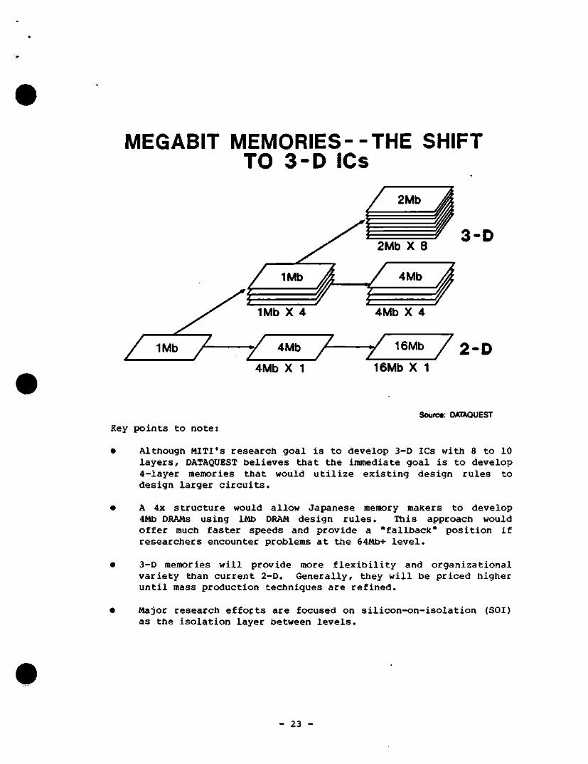
MEGABIT MEiVIORIES--THE SHIFT TO 3-D ICs
16Mb
3-D
4Mb X 1 16Mb X 1 72-D
Source: DAIAQUEST
Key points to note:
Alttiough MITI's research goal is to develop 3-D ICs with 8 to 10 layers, DATAQUEST believes that the immediate goal is to develop 4-layer memories that would utilize existing design rules to design larger circuits.
A 4x structure would allow Japanese memory makers to develop 4Mb DRAMS using 1Mb DRAM design rules. Ttiis approach would Offer much faster speeds and provide a "fallback" position if researchers encounter problems at the 64Mb+ level.
3-D memories will provide more flexibility and organizational variety than current 2-D. Generally, they will be priced higher until mass production techniques are refined.
Major research efforts are focused on silicon-on-isolation (SOI) as the isolation layer between levels.
- 23 -
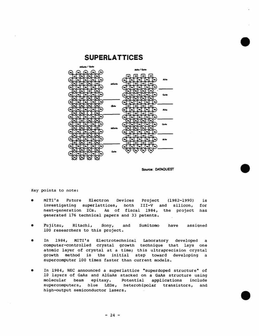
SUPERLATTICES MitoXCUto
Zv* (A>
( A .
(^
JU
M
4
r%^j imy
b
h
M
Al
y
ito
'A .
^
G^ <>• M
Al
Al
y A.
Al
Al
^
A>)
* • )
^
Key points to note:
Sourcs: DATAQUE5T
MITI's Future Electron Devices Project (1982-1990) is investigating superlattices, botti III-V and silicon, for next-generation ICs. As of fiscal 1984, the project has generated 176 technical papers and 33 patents.
Fujitsu, Hitachi, Sony, and 100 researchers to this project.
Sumi tomo have assigned
In 1984, MITI's Electrotechnical Laboratory developed a computer-controlled crystal growtti technique that lays one atomic layer of crystal at a time; this ultraprecision crystal growth method is the initial step toward developing a supercomputer 100 times faster than current models.
In 1984, NEC announced a superlattice "superdoped structure" of 10 layers of GaAs and AlGaAs stacked on a GaAs structure using molecular beam epitaxy. Potential applications include supercomputers, blue LEDs, tieterobipolar transistors, and high-output semiconductor lasers.
- 24 -
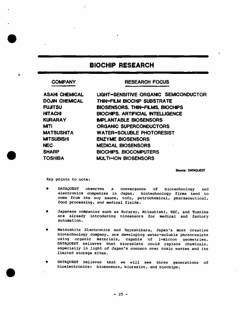
BIOCHIP RESEARCH
COMPANY
ASAHI CHEMICAL OOJIN CHEMICAL FUJITSU HITACHI KURARAY MITI MATSUSHITA MITSUBISHI NEC SHARP TOSHIBA
RESEARCH FOCUS
LIGHT-SENSITIVE ORGANIC SEMICONDUCTOR THIN-FILM BIOCHP SUBSTRATE BIOSENSORS. THIN-FILMS. BIOCHPS BIOCHIPS. ARTFICIAL INTELUGENCE IMPLANTABLE BIOSENSORS ORGANIC SUPERCONDUCTORS WATER-SOLUBLE PHOTORESIST ENZYME BIOSENSORS MEDICAL BIOSENSORS BIOCHIPS. BIOCOMPUTERS MULTI-ION BIOSENSORS
Source: DATAQUEST
Key points to note:
DATAQUEST observes a convergence of biotechnology and electronics companies in Japan. Biotechnology firms tend to come from the soy sauce, tofu, petrochemical, ptiarmaceutical, food processing, and medical fields.
Japanese companies such as Kuraray, Mitsubishi, NEC, and Tostiiba are already introducing biosensors for medical and factory automation.
Matsushita Electronics and Hayashibara, Japan's most creative biotechnology company, are developing water-soluble photoresists using organic materials, capable of 1-micron geometries. DATAQUEST believes that bioresists could replace chemicals, especially in light of Japan's concern over toxic wastes and its limited storage sites.
DATAQUEST believes that we will see three generations of bioelectronics: biosensors, bioresist, and biochips.
- 25 -
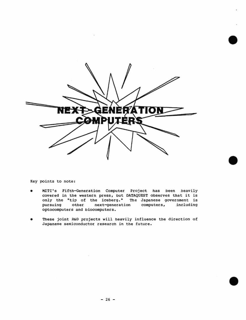
Key points to note:
• MITI's Fifth-Generation Computer Project has been heavily covered in the western press, but DATAQUEST observes that it is only the "tip of the iceberg." The Japanese government is pursuing other next-generation computers, including optocomputers and biocomputers.
• These joint R&D projects will heavily influence the direction of Japanese semiconductor research in the future.
- 26 -
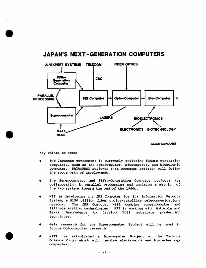
JAPAN'S NEXT-GENERATION COMPUTERS
AI/EXPERT SYSTEMS TELECOM
1 FIBER OPTICS
Fifth-Generation Computer
PARALLEL PROCESSING
K C&C
MS Computer
Supercomputer V
-*• Opto-Computer -*• Bio-Computer
LASERS /
BIOELECTRONICS
y N ELECTROfiflCS BIOTECHNOLOGY
Source: OAIAQUEST
Key points to note:
The Japanese government is currently exploring future generation computers, such as the optocomputer, biocomputer, and bioholonic computer. DATAQUEST believes that computer research will follow the above path of development.
The Supercomputer and Fifth-Generation Computer projects are collaborating in parallel processing and envision a merging of the two systems toward the end of the 1980s.
NTT is developing the INS Computer for its Information Network System, a $150 billion fiber optics-satellite telecommunications network. The INS Computer will combine supercomputer and fifth-generation technologies. NTT is working with Motorola and Texas Instruments to develop VLSI substrate production techniques.
GaAs research for the Supercomputer Project will be used in future Optocomputer research.
MITI has established a Biocomputer Project at the Tsukuba Science City, which will involve electronics and biotechnology companies.
- 27 -
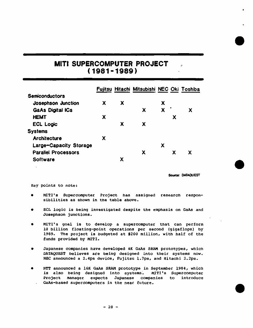
MITI SUPERCOMPUTER PROJECT (1981-1989)
Fujitsu Hitachi Mitsubishi NEC Oki Toshiba Semiconductors
Josephson Junction GaAs Digital ICs HEMT ECL Logic
Systems Architecture Large-Capacity Storage Parallel Processors Software
X
X
X
X
X
X
X
X
X
X X
X
Source: OATAOUEST
Key points to note:
MITI's Supercomputer Project has assigned research responsibilities as shown in the table above.
ECL logic is being investigated despite the emphasis on GaAs and Josephson junctions.
MITI's goal is to develop a supercomputer that can perform 10 billion floating-point operations per second (gigaflops) by 1989. The project is budgeted at $200 million, with half of the funds provided by MITI.
Japanese companies have developed 4K GaAs SRAM prototypes, which DATAQUEST believes are being designed into their systems now. NEC announced a 2.4ps device, Fujitsu 1.7ps, and Hitachi 2.2ps.
NTT announced a 16K GaAs SRAM prototype in September 1984, which is also being designed into systems. MITI's Supercomputer Project manager expects Japanese companies to introduce GaAs-based supercomputers in the near future.
- 28 -
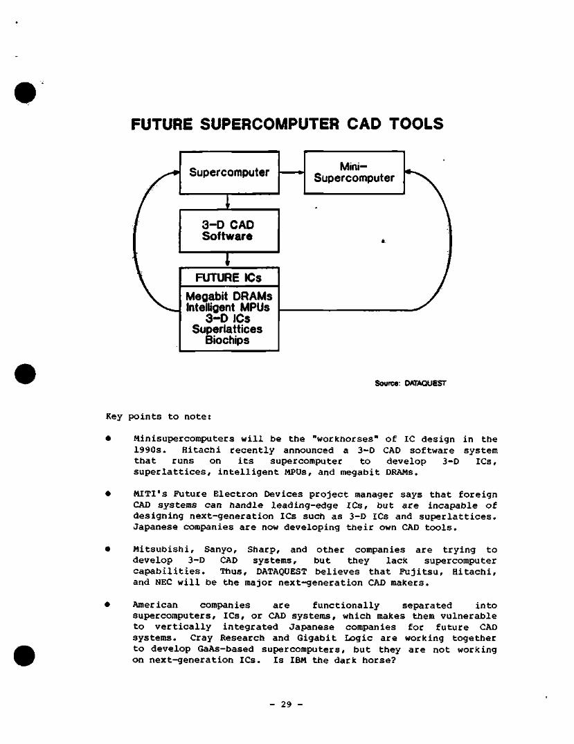
FUTURE SUPERCOMPUTER CAD TOOLS
Supercomputer
3-D CAD Software
FUTURE ICs
Megabit DRAMs intelligent MRUs
3-D ICs Superlattices
Biochips
Mini-Supercomputer
Source: OATAQUEST
Key points to note;
• Minisupercomputers will be the "workhorses" of IC design in the 1990s. Hitachi recently announced a 3-D CAD software system ttiat runs on its supercomputer to develop 3-D ICs, superlattices, intelligent MPUs, and megabit DRAMs.
• MlTI's Future Electron Devices project manager says that foreign CAD systems can tiandle leading-edge ICs, but are incapable of designing next-generation ICs such as 3-D ICs and superlattices. Japanese companies are now developing their own CAD tools.
• Mitsubishi, Sanyo, Sharp, and other companies are trying to develop 3-D CAD systems, but they lack supercomputer capabilities. Thus, DATAQUEST believes that Fujitsu, Hitachi, and NEC will be the major next-generation CAD makers.
• American companies are functionally separated into supercomputers, ICs, or CAD systems, which makes them vulnerable to vertically integrated Japanese companies for future CAD systems. Cray Research and Gigabit Logic are working together to develop GaAs-based supercomputers, but they are not working on next-generation ICs. Is IBM the dark horse?
- 29 -
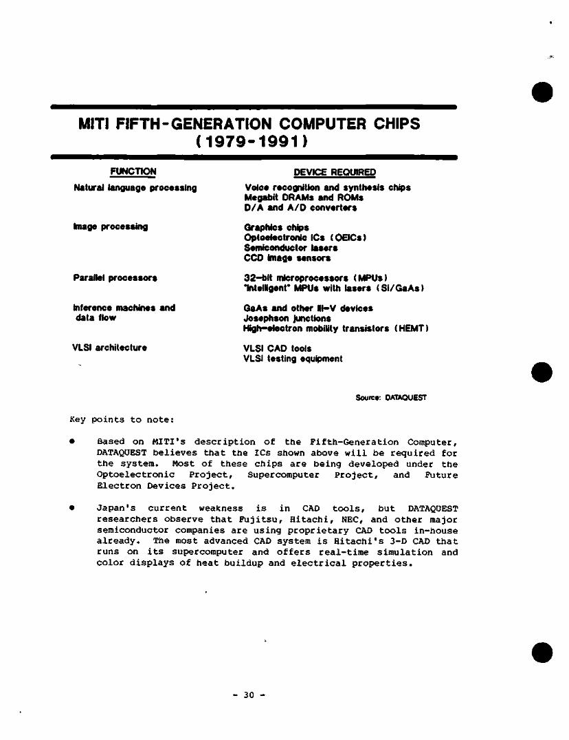
MITI FIFTH-GENERATION COMPUTER CHIPS (1979-1991)
FUNCTION
Natural language processing
bnage processing
Parallel processors
Inference machines and data flow
VLSI architecture
DEVICE REQUIRED
Voice recognition and synthesis chips Megabit ORAMs and ROMs D/A and A/D converters
Graphics chips Optoelectronie ICs (OEICs) Semiconductor lasers c e o Image sensors
32-bit microprocessors (MPUs) 'InteIHgenr MPUs with lasers (Si/GaAs)
GaAs and other Hl-V devices Josephson Junctions High-electron mobility transistors (HEMT)
VLSI CAD tools VLSI testing equipment
Source: DATAQUEST
Key points to note:
e Based on Mill's description of the Fifth-Generation Computer, DATAQUEST believes that the ICs shown above will be required for the system. Most of these chips are being developed under the Optoelectronic Project, Supercomputer Project, and Future Electron Devices Project.
e Japan's current weakness is in CAD tools, but DATAQUEST researchers observe that Fujitsu, Hitachi, NEC, and other major semiconductor companies are using proprietary CAD tools in-house already. The most advanced CAD system is Hitachi's 3-D CAD that runs on its supercomputer and offers real-time simulation and color displays of heat buildup and electrical properties.
30 -
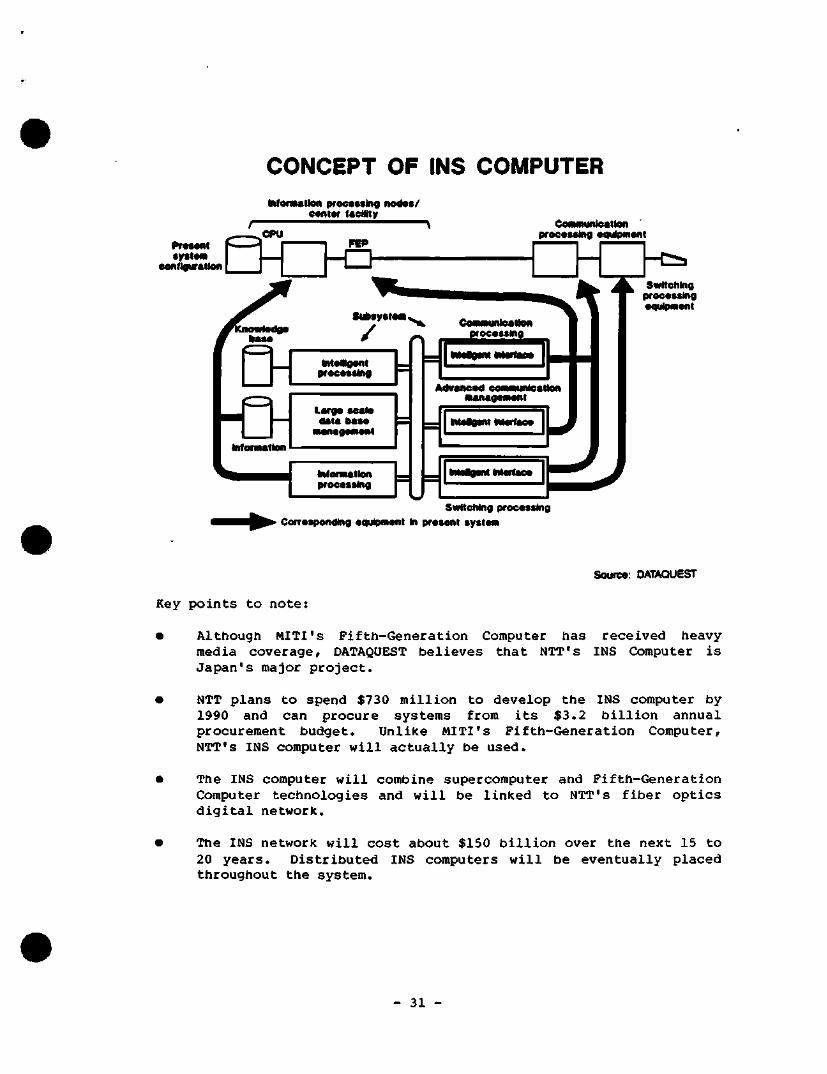
CONCEPT OF INS COMPUTER kiformallon processing nod«s/
c«nt«r UcWty
Pr««Mit •ystMn
configuration ffl FEP
CoNMHinlcatton precossing oqu^mont
WKnomim^gt^
' Jis?
Switching processing oqulpmont
::—;
kiloMgant precosting
Largo seal* da la baa*
Monagotnoni
Inlonnailofl procatsfeig
SwitcMng processing Corresponding equipmoni In present system
Source: OATAQUEST
Key points to note:
Although Mill's Fifth-Generation Computer has received heavy media coverage, OATAQUEST believes that NTT's Japan's major project.
INS Computer is
NTT plans to spend $730 million to develop the INS computer by 1990 and can procure systems from its $3.2 billion annual procurement budget. Unlike MITI's Fifth-Generation Computer, NTT's INS computer will actually be used.
The INS computer will combine supercomputer and Fifth-Generation Computer technologies and will be linked to NTT's fiber optics digital network.
The INS network will cost about $150 billion over the next 15 to 20 years. Distributed INS computers will be eventually placed throughout the system.
- 31 -
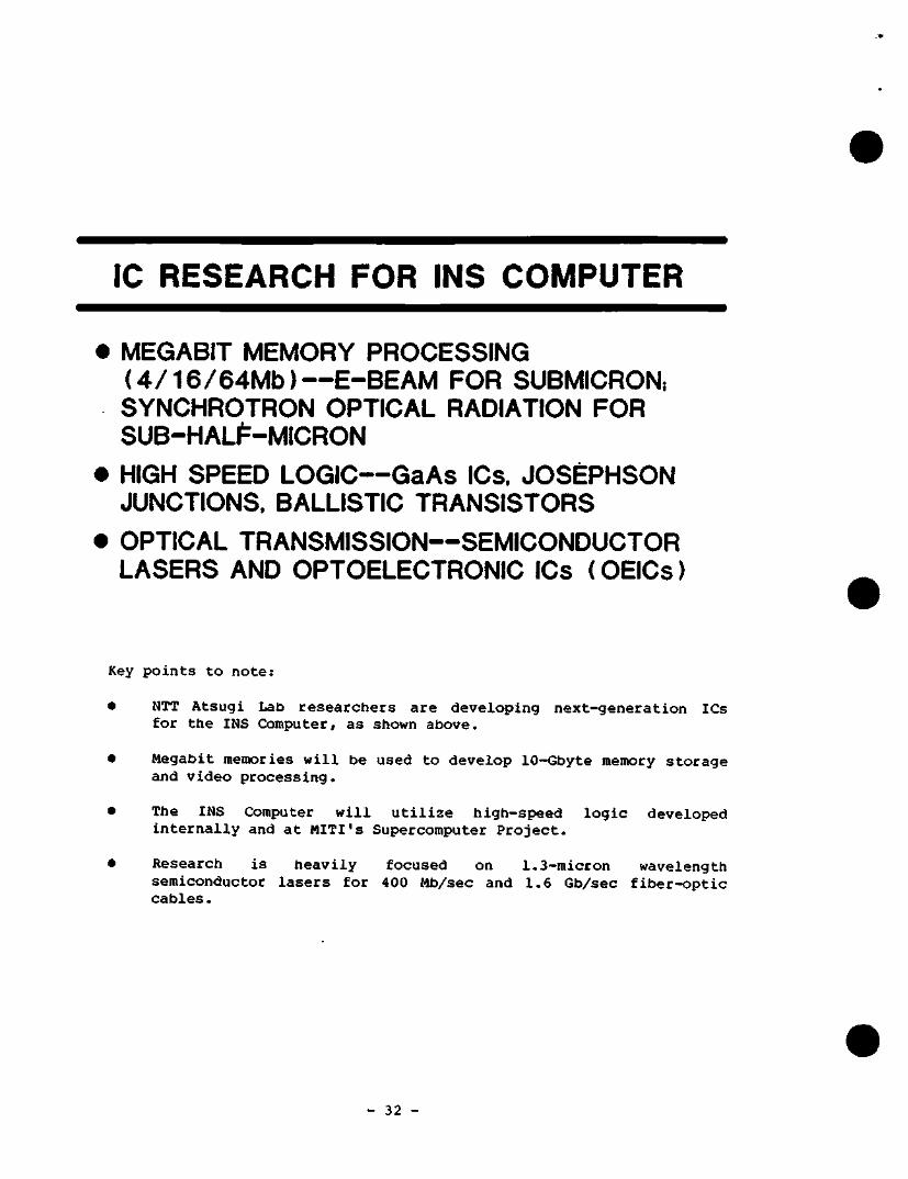
IC RESEARCH FOR INS COMPUTER
MEGABIT MEMORY PROCESSING (4/16/64Mb)—E-BEAM FOR SUBMICRON; SYNCHROTRON OPTICAL RADIATION FOR SUB-HALf-MICRON HIGH SPEED LOGIC—GaAs ICs. JOSEPHSON JUNCTIONS. BALLISTIC TRANSISTORS OPTICAL TRANSMISSION—SEMICONDUCTOR LASERS AND OPTOELECTRONIC ICs (OEICs)
Key points to note:
• NTT Atsugi Lab researchers are developing next-generation ICs for the INS Computer, as shown above.
• Megabit memories will be used to develop 10-Gbyte memory storage and video processing.
• The INS Computer will utilize higti-speed logic developed internally and at MITI's Supercomputer Project.
• Research is heavily focused on 1.3-micron wavelength semiconductor lasers for 400 Mb/sec and 1.6 Gb/sec fiber-optic cables.
- 32 -
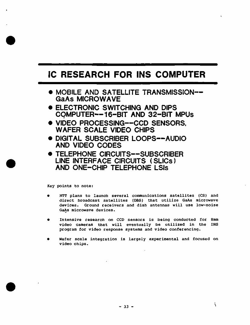
IC RESEARCH FOR INS COMPUTER ^^^^^^^^^^^^^^^^^^^^^^^^^^^^^^^^^^^i^^^^^l^^^^^^^H^^^^^^^^H^^^^H^BM^^^^^^P
• MOBILE AND SATELLITE TRANSMISSION— GaAs MICROWAVE
• ELECTRONIC SWITCHING AND DIPS COMPUTER—16-BIT AND 32-BIT MPUs
• VIDEO PROCESSING~CCD SENSORS. WAFER SCALE VIDEO CHIPS
• DIGITAL SUBSCRIBER LOOPS—AUDIO AND VIDEO CODES
• TELEPHONE CIRCUITS—SUBSCRIBER LINE INTERFACE CIRCUITS (SLICs) AND ONE-CHIP TELEPHONE LSIs
Key points to note:
• NTT plans to launch several communications satellites (CS) and direct broadcast satellites (DBS) that utilize GaAs microwave devices. Ground receivers and dish antennas will use low-noise GaAs microwave devices.
• Intensive research on CCD sensors is being conducted for 8mm video cameras t:tiat will eventually be utilized in the INS program for video response systems and video conferencing.
• Wafer scale integration is largely experimental and focused on video chips.
- 33 -
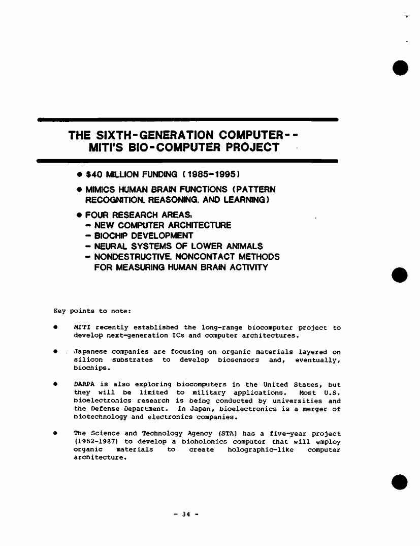
THE SIXTH-GENERATION COMPUTER-MirrS BIO-COMPUTER PROJECT
• $40 MILLION FUNDING (1985-1995)
• MIMICS HUMAN BRAIN FUNCTIONS (PATTERN RECOGNITION. REASONING. AND LEARNING)
• FOUR RESEARCH AREAS. - NEW COMPUTER ARCHITECTURE - BIOCHIP DEVELOPMENT - NEURAL SYSTEMS OF LOWER ANIMALS - NONDESTRUCTIVE. NONCONTACT METHODS
FOR MEASURING HUMAN BRAIN ACTIVITY
Key points to note:
• MITI recently established ttie long-range biocomputer project to develop next-generation ICs and computer a rch i t ec tu res .
• Japanese companies are focusing on organic mater ials layered on s i l i con substra tes to develop biosensors and, eventual ly, biochips.
• DARPA i s a lso exploring biocomputers in the United S ta t e s , but they wi l l be limited to mi l i ta ry appl ica t ions . Most U.S. bioelectronics research i s being conducted by un ive r s i t i e s and the Defense Department. In Japan, bioelectronics i s a merger of biotechnology and e lec t ronics companies.
• Ttie Science and Technology Agency (STA) has a five-year project (1982-1987) to develop a bioholonics computer that wi l l employ organic materials to create holographic-l ike computer a r ch i t ec tu re .
- 34 -
Key points to note:
• Despite fierce price competition from Japan, there are numerous market opportunities for foreign companies. What are these?
Joint R&D with NTT and subsequent sales of systems
Strategic alliances in specific markets (e.g., ASICs)
Development and sales of advanced CAD tools for next-generation ICs
Semiconductor equipment for next-generation ICs
Design-in of semiconductors in tJ.S. telecommunications equipment tailored to the Japanese market
Development of next-generation ICs (speech synthesis and recognition, video processing, expert systems, etc.)
• DATAQUEST believes that U.S. and European makers must establish a major presence in Japan to remain competitive internationally.
- 35 -
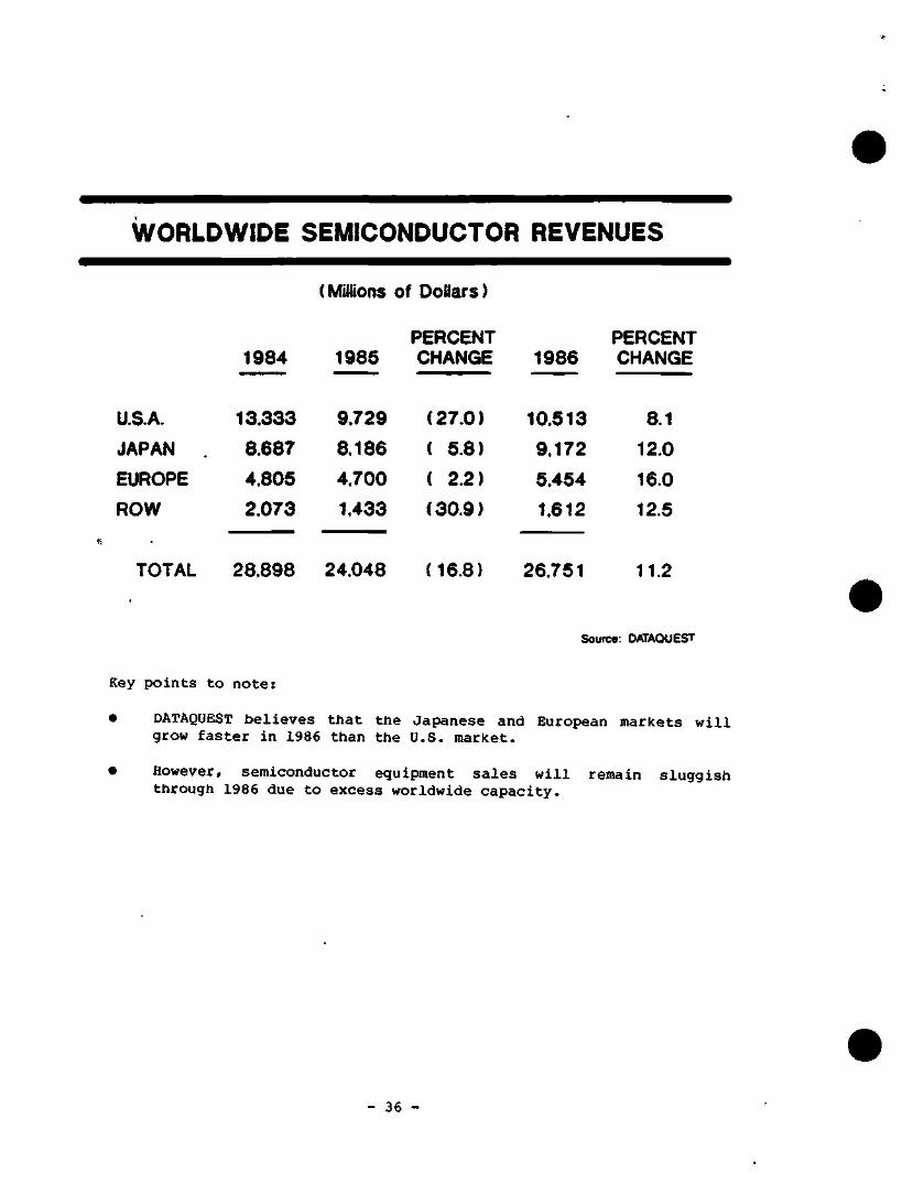
WORLDWIDE SEMICONDUCTOR REVENUES
(Millions of Dollars)
PERCENT PERCENT 1984 1985 CHANGE 1986 CHANGE
U.S.A.
JAPAN
EUROPE
ROW
13.333
8.687
4.805
2.073
9.729
8.186
4.700
1.433
(27.0)
( 5.8)
( 2.2)
(30.9)
10.513
9.172
5.454
1.612
8.1
12.0
16.0
12.5
TOTAL 28.898 24.048 (16.8) 26.751 11.2
Source: DATAQUEST
Key points to note:
• DATAQUEST believes ttiat ttie Japanese and European markets will grow faster in 1986 than the U.S. market.
• However, semiconductor equipment sales will remain sluggish through 1986 due to excess worldwide capacity.
- 36 -
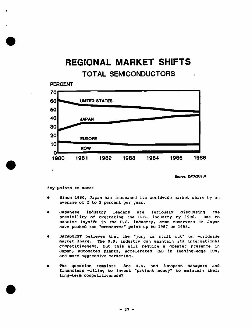
REGIONAL MARKET SHIFTS TOTAL SEMICONDUCTORS
PERCENT
70
1980
U^aTED STATES
ROW
1981 1982 1983 1984 1985 1986
Source: DATAQUEST
Key points to note:
• Since 1980, Japan has increased its worldwide market share by an average of 2 to 3 percent per year.
• Japanese industry leaders are seriously discussing the possibility of overtaking the U.S. industry by 1990. Due to massive layoffs in the tJ.S. industry, some observers in Japan tiave pushed the "crossover" point up to 1987 or 1988.
• DATAQUEST believes that ttie "jury is still out" on worldwide market stiace. The U.S. industry can maintain its international competitiveness, but ttiis will require a greater presence in Japan, automated plants, accelerated R&D in leading-edge ICs, and more aggressive marketing.
• The question remains: Are U.S. and European managers and financiers willing to invest "patient money" to maintain their long-term competitiveness?
- 37 -
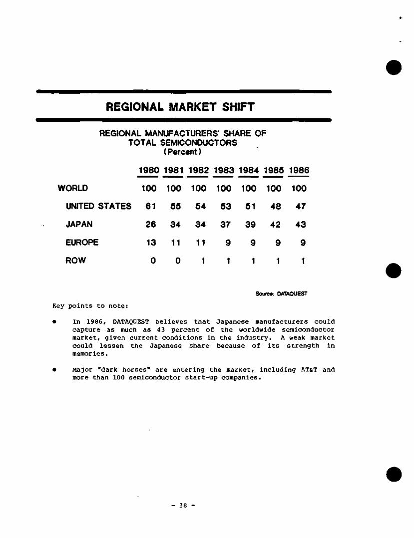
REGIONAL MARKET SHIFT
REGIONAL MANUFACTURERS' SHARE OF TOTAL SEMICONDUCTORS
(Percent)
1980 1981 1982 1983 1984 1985 1986
WORLD 100 100 100 100 100 100 100
UNITED STATES 61 55 64 53 51 48 47
JAPAN 26 34 34 37 39 42 43
EUROPE 13 11 11 9 9 9 9
ROW 0 0 1 1 1 1 1
Sourcs: OATAQUEST
Key points to note:
In 1986, DATAQUEST believes that Japanese manufacturers could capture as much as 43 percent of the worldwide semiconductor market, given current conditions in the industry. A weak market could lessen the Japanese share because of its strength in memories.
Major "dark horses" are entering the market, including AT&T and more than 100 semiconductor start-up companies.
- 38 -
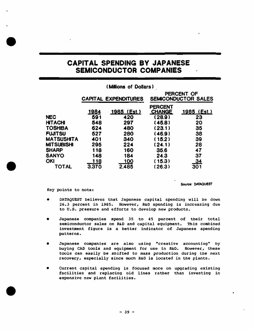
CAPITAL SPENDING BY JAPANESE SEMICONDUCTOR COMPANIES
(Millions of Dollars) PERCENT OF
CAPITAL EXPENDITURES SEMICONDUCTOR SALES
NEC HITACHI TOSHIBA FUJITSU MATSUSHITA MITSUBISHI SHARP SANYO OKI
TOTAL
1984 591 548 624 527 401 295 118 148 118
3.370
1985 CEst.) 420 297 480 280 340 224 160 184 100
2.485
PERCENT CHANGE
(28.9) (45.8) (23.1) (46.9) (15.2) (24.1) 35.6 24.3
(15.3) (26.3)
1985 (Est.) 23 20 35 38 39 28 47 37 34
301
Source: OATAQUEST
Key points to note:
• OATAQUEST believes that Japanese capital spending will be down 26.3 percent in 1985. However, R&D spending is increasing due to U.S. pressure and efforts to develop new products.
• Japanese companies spend 35 to 45 percent of their total semiconductor sales on R&D and capital equipment. This combined investment figure is a better indicator of Japanese spending patterns.
• Japanese companies are also using "creative accounting" by buying CAD tools and equipment for use in R&D. However, ttiese tools can easily be shifted to mass production during the next recovery, especially since much R&D is located in the plants.
• Current capital spending is focused more on upgrading existing facilities and replacing old lines rather than investing in expensive new plant facilities.
- 39 -
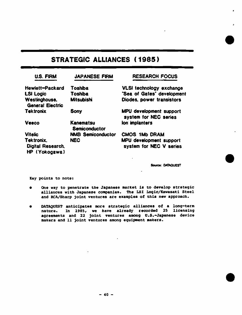
STRATEGIC ALLIANCES (1985)
U.S. FIRM JAPANESE FIRM RESEARCH FOCUS
Hewlett-Packard LSI Logic Westinghouse. General Electric
Tektronix
Veeco
Viielic Tektronix. Digital Research. HP (Yokogawa)
Toshiba Toshiba Mitsubishi
Sony
Kanematsu Semiconductor
NMB Semiconductor NEC
VLSI technology exchange *Sea of Gates* development Diodes, power transistors
MPU development support system for NEC series
Ion implanters
CMOS 1Mb DRAM MPU development support system for NEC V series
Soum: OXrAOUEST
Key points to note:
• One way to penetrate ttie Japanese market is to develop strategic alliances with Japanese companies. Ttie LSI Logic/Rawasaki Steel and RCA/Stiarp joint ventures are examples of ttiis new approacti.
• DATAQUEST anticipates more strategic alliances of a long-term nature. In 1985, we tiave already recorded 25 licensing agreements and 22 joint ventures anong D.S.-Japanese device makers and 11 joint ventures among equipment makers.
- 40 -
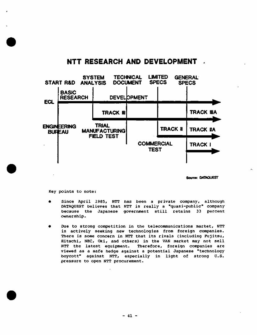
NTT RESEARCH AND DEVELOPMENT
SYSTEM TECHNICAL UMITED GENERAL START R&D ANALYSIS DOCUMENT SPECS SPECS
ECL
BASIC RESEARCH DEVEL DPMENT
TRACK 111
ENGINtERING TRIAL BUR EAU MANUFACTURING
FELD TEST
TRACK II
COMMERaAL TEST
TRACK HIA
TRACK HA
TRACK I
Source: OAFAOUEST
Key points to note:
• Since April 1985, NTT has been a private company, although DATAQUEST believes that NTT is really a "quasi-public" company because the Japanese government still retains 33 percent ownership.
• Due to strong competition in the telecommunications market, NTT is actively seeking new technologies from foreign companies. There is some concern in NTT that its rivals (including Fujitsu, Hitachi, NEC, Oki, and others) in the VAN market may not sell NTT the latest equipment. Therefore, foreign companies are viewed as a safe hedge against a potential Japanese "technology boycott" against NTT, especially in light of strong U.S. pressure to open NTT procurement.
- 41 -
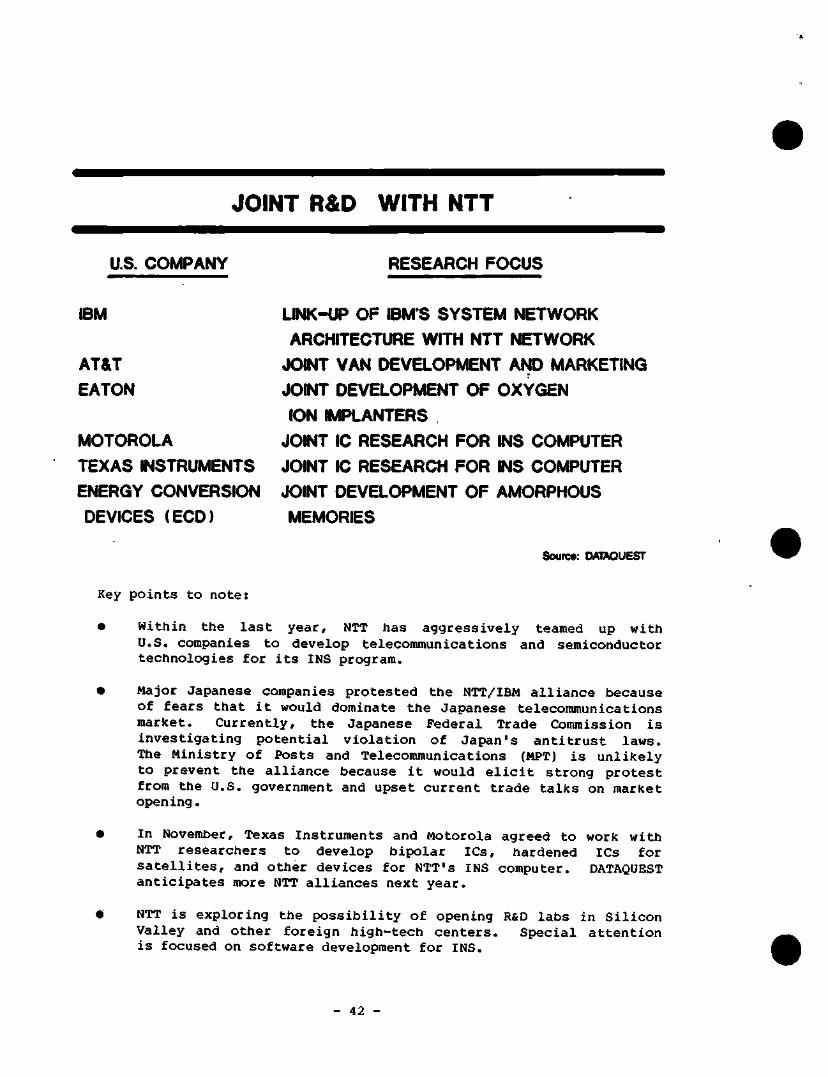
JOINT R&D WITH NTT
U.S. COMPANY RESEARCH FOCUS
IBM
AT&T EATON
MOTOROLA
TEXAS INSTRUMENTS ENERGY CONVERSION DEVICES (ECD)
LINK-UP OF IBM'S SYSTEM NETWORK ARCHITECTURE WITH NTT NETWORK
JOINT VAN DEVELOPMENT AND MARKETING JOINT DEVELOPMENT OF OXYGEN ION IMPLANTERS
JOINT IC RESEARCH FOR INS COMPUTER JOINT IC RESEARCH FOR INS COMPUTER JOINT DEVELOPMENT OF AMORPHOUS MEMORIES
Source: OATAOUEST
Key points to note:
• Within the last year, NTT has aggressively teamed up with U.S. companies to develop telecommunications and semiconductor technologies for its INS program.
• Major Japanese companies protested the NTT/IBM alliance because of fears that it would dominate the Japanese telecommunications marlcet. Currently, the Japanese Federal Trade Commission is investigating potential violation of Japan's antitrust laws. The Ministry of Posts and Telecommunications (MPT) is unlikely to prevent the alliance because it would elicit strong protest from the U.S. government and upset current trade talks on market opening.
• In November, Texas Instruments and Motorola agreed to work with NTT researchers to develop bipolar ICs, hardened ICs for satellites, and other devices for NTT's INS computer. DATAQUEST anticipates more NTT alliances next year.
0 NTT is exploring the possibility of opening R&D labs in Silicon Valley and other foreign high-tech centers. Special attention is focused on software development for INS.
- 42 -
SUMMARY
• Japanese companies are emphasizing creative research; creativity is Japan's industrial slogan for the 1980s.
• Research is rapidly proceeding on next-generation IC technologies, including 3-D ICs, superlattices, GaAs, and bioelectronics.
• MITI officials emphasize the lack of sophisticated CAD tools to develop these next-generation ICs. As a result, Japanese companies are developing them in-house. DATAQtJEST believes that next-generation CAD tools will be "Personal Grays" (PCs) or desktop supercomputers.
• Although media attention is focused on MITI's Fifth-Generation Computer, the real research in future computing is being conducted by NTT and the corporate labs.
• The INS Computer will combine supercomputer and Fifth-Generation Computer technology.
• Initial work is beginning on optocomputers and biocomputers.
• American companies, especially start-ups, are developing the semiconductors needed for Japan's next-generation computers. Now is the time to capitalize on these technologies by strategically entering joint ventures without "giving away the store."
• NTT is aggressively pursuing foreign R&D partners under its Track III procurement guidelines. AT&T, IBM, Motorola, and Texas Instruments are already signed up. DATAQUEST anticipates more joint ventures and licensing by NTT in the future.
• Given the growing strength of the Japanese semiconductor industry, foreign companies have two choices: "ride the wave" or be demolished by the coming Japanese wave. The survivors will be those companies that have strategically positioned themselves to take advantage of Japan's mass production capabilities and next-generation IC research. A good example is IBM's agreement to license patents from MITI's next-generation projects.
Sheridan Tatsuno
- 43 -
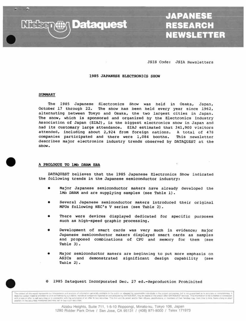
JSIS Code: JSIA Newsletters
1985 JAPANESE ELECTRONICS SHOW
SUMMARY
The 1985 Japanese Electronics Show was held in Osaka, Japan, October 17 through 22. The show has been held every year since 1962, alternating between Tokyo and Osaka, the two largest cities in Japan. The show, which is sponsored and organized by the Electronics Industry Association of Japan (EIAJ), is the biggest electronics show in Japan and had its customary large attendance. EIAJ estimated that 341,900 visitors attended, including about 2,924 from foreign nations. A total of 478 companies participated and there were 1,084 booths. This newsletter describes major electronics industry trends observed by DATAQUEST at the show.
A PROLOGUE TO 1Mb DRAM BRA
DATAQUEST believes that the 1985 Japanese Electronics Show indicated the following trends in the Japanese semiconductor industry:
• Major Japanese semiconductor makers have already developed the 1Mb DRAM and are supplying samples (see Table 1).
• Several Japanese semiconductor makers introduced their original MPUs following NEC's V series (see Table 2).
• There were devices displayed dedicated for specific purposes such as high-speed graphic processing.
• Development of smart cards was very much in evidence; major Japanese semiconductor makers displayed smart cards as samples and proposed combinations of CPU and memory for them (see Table 3) .
• Major semiconductor makers are beginning to put more emphasis on ASICs and demonstrated significant design capability (see Table 2) .
1985 Dataquest Incorporated Dec. 27 ed.-Reproduction Prohibited
The content of this report represents our interprelaion and analysis of information generally available to the public or released by responsible individuals in the subject companies, but is not guaranteed as to accuracy or completeness It does not contain material provided to us in confidence by our clients Individual companies reported on and anaIyzed by DATAQUEST, may be clients ot this and/or other DATAQUEST services This information is not furnished in connection with a sale or offer lo sell securities or in connection with the solicitation of an offer to buy securities This firm and its parent and/or their officers, stockholders, or members of their families may, from time to lime, have a long or short position in the securities mentioned and may sell or buy such securities
Azabu Heights, Suite 711, 1-5-10 Roppongi, Minato-ku, Tokyo 106, Japan 1290 Bidder Park Drive / San Jose, CA 95131 / (408) 971-9000 / Telex 171973
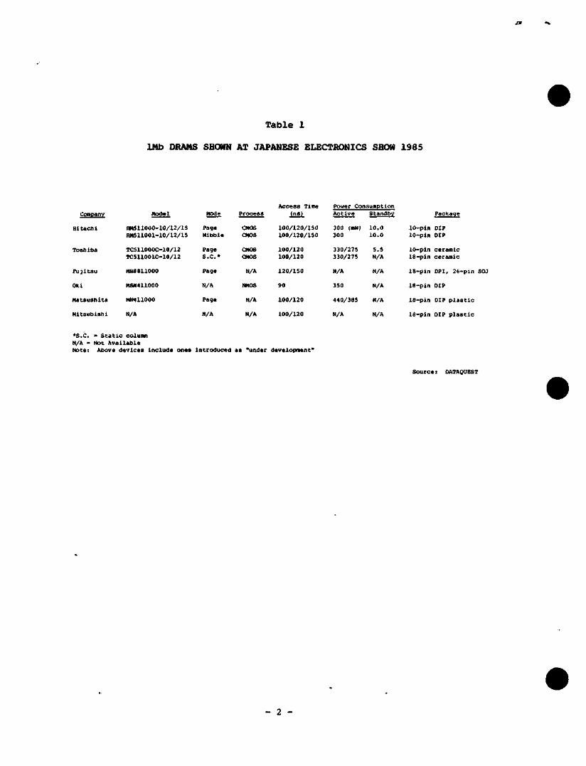
Table 1
1Mb DRAMS SHOWN AT JAPANESE ELECTRONICS SHOW 1985
Company
Hitacni
Tosh iba
Fujitsu
Oki
Matsushita
Mitsubishi
Model
HMSllOOO-10/12/15 HM511001-10/12/15
TCSllOOOC-10/12 TC51100iC-10/12
HB8811000
HSH41ia00
MN4110aO
N/A
Mode
Page Nibble
Page S.C.*
Page
N/A
Page
N/A
Process
CMOS CMOS
CMOS CMOS
N/A
NMOS
N/A
N/A
Access Time
(ns)
100/120/150
100/120/150
100/120 100/120
120/150
90
100/120
100/120
Power Consumption Active
300 (mH) 300
330/275 330/275
N/A
350
440/385
N/A
Standby
10.0 10.0
5.5 N/A
N/A
N/A
N/A
N/A
10-pin 10-pln
10-pln 18-pin
18-pin
18-pin
18-pin
18-pln
Package
DIP DIP
ceramic ceramic
DPI, 26-pin SOJ
DIP
DIP plastic
DIP plastic
*S.C. . static column N/A - Not Available
Note; Above devices include ones introduced as *under development*
Source: OATAQUEST
- 2 -
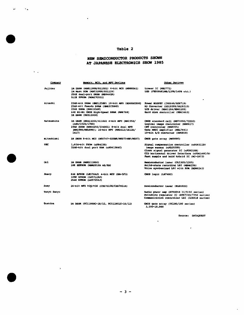
Table 2
NEW SBHICONOUCTOR PRODUCTS SHOWN AT JAPANESE ELECTRONICS SHOW 1985
Company
Fujitsu
Matsushita
Mitsubishi
NBC
OKi
Sharp
Sony
Tokyo Sanyo
Memory, MCU, and MPU Devices
IM DRAM (MBSllOOO/ailOOl) 4-blt HCU (MB88S61) IM Hasic ROM (Mfi83100a/831124) 2S6K dual-port DRAM (HB9461A) S12K EFROM (HOH27CS12)
2S6K-0it DRAM (BMS12S8F) 16-bit MPU (HO68aC000) 2S6K-bit Pseudo SRAM (HH6S2SGAP) 2S6K SRAM (HHe22S«P) 64K Hi-Bi CMOS Bi9b-Speed SRAM (HM6768) IH DRAM (HflSllOOO)
IM DRAM (MN411000/4110al 4-bit HPU (MN1S50/ 1480/1520/1700) 2S6K SRAM (NN442S6/234001) 8-blt dual HPO (HN1880/MN1890); 16-bit HPU (MN1613/1613A/ 1617)
Other Devices
Linear IC (H83771) LEO (PBD086KlHB/L3PB/L4Pa etc.)
Power HOSFET (28K646/HS8719) AO Converter (HD19209/HA19210) LCD driver (HO61104/HDeil0S) Bard disk controller (a063463)
CMOS standard cell (HN7100O/720O0) Logical image controller (HNSei7) CRT controller (HN8355) GaAs HMIC amplifier (MEL7441) 10-bit A/D converter (AN68S9)
IH ORAH 8-blt MCU (HS0747-XXXBP/MS0734BP/M507) OtOS gate array (M60000)
1,024-bit PRQH (UPB423G) 2S6K-blt dual port RAN (uP041264C)
IH ORAM (HSHlllOOO) 1«K BEPROH (HBn2816A AS/RB)
«4K EPSOM (LaS764J) 4-bit HCD (fiM-5F3) 128K EPROH (LHS7128J) 256K EPROH (LBS7256J)
16-bit HPU V2P/V30 (CXG70ia8/CXG70116)
IM DRAM (TCllOOOC-10/12, TCSllOOlC-10/12)
Signal compensation controller (uP09311B) image sensor (uPD3S20D)
Clock signal generator IC (uPD9310B) CCO horizontal driver interface (uP06146C/B) Fast sample and hold hybrid IC (HC-5973)
Semiconductor laser (OLI305/1205) Solid-state recording LSI (HBH6258) Voice synthesized LSI with ROM (HSH6243)
CMOS logic (LR74HC)
Semiconductor laser (BLOIOIU)
Audio power amp (BTK4044 II/V/XI series) Switching regulator IC (BTK7340/7350 secies) Communication controller LBI (LC8910 series)
CMOS gate array (TC18Q/190 series) 3,200-10,000
Source: DATAQUEST
- 3 -
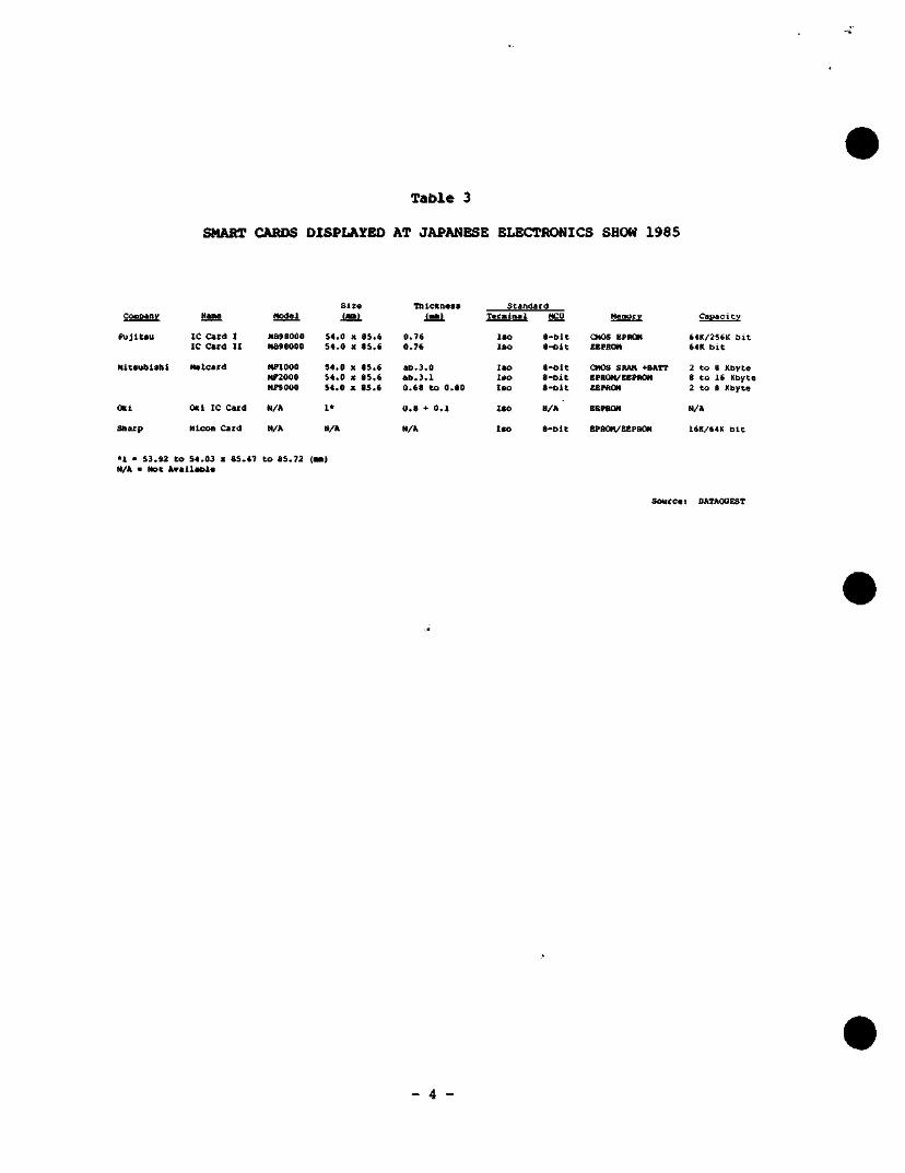
Table 3
SMART CARDS DISPLAYED AT JAPANESE ELECTRONICS SHOW 1985
Company
Fujitsu
Mitsubishi
Oki
Sharp
Name
IC Card I IC Card II
Melcard
Oki IC Card
Hicon Card
Model.
HB98000 MS98000
HFIOOO MF2aOO MF5000
N/A
N/A
Size (ran)
54 .0 X 85.6 54.0 X 85.6
54.0 X 85.6 54.0 X 85.6 54 .0 X 85.6
1*
N/A
Thickness
iasi. 0.76 0.76
aD.3.0 ah.3.1 0.68 to 0.
0.8 + 0.1
N/A
.80
standard Terminal
ISO ISO
ISO ISO ISO
Zso
ISO
HCU
8-bit 8-bit
8-blt 8-blt 8-bit
N/A
8-bit
Memory
CMOS EPROM EEPSOM
CMOS SSAM -t-BATT EPH0M/EEP80N EEPROM
EEPRQM
EPROH/EEPROM
Capacity
64K/2S6K bit 64K bit
2 to a Kbyte 8 to 16 Kbyte 2 to 8 Kbyte
N/A
16X/64K bit
•1 • 53.92 to 54.03 x 85.47 to 85.72 (on) N/A • Not Available
Source; DATAOUBST
- 4 -
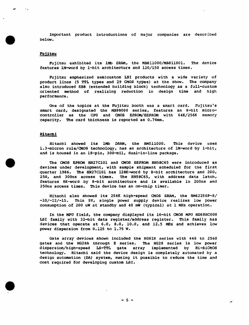
Important product introductions of major companies are described below.
Fujitsu
Fujitsu exhibited its 1Mb DRAM, the MB811000/MB811001. The device features IM-word by 1-bit architecture and 120/150 access times.
Fujitsu emphasized semicustom LSI products with a wide variety of product lines (5 TTL types and 29 CMOS types) at the show. The company also introduced EBB (extended building block) technology as a full-custom oriented mettiod of realizing reduction in design time and high performance.
One of ttie topics at the Fujitsu booth was a smart card. Fujitsu's smart card, designated the MB98000 series, features an 8-bit microcontroller as the CPU and CMOS EPROM/EEPROM with 64K/256K memory capacity. The card thickness is reported as 0.76mm.
Hitachi
Hitachi showed its 1Mb DRAM, the HM511Q00. This device uses 1.3-micron rule/CMOS technology, has an architecture of IM-word by 1-bit, and is housed in an 18-pin, 300-mil, dual-in-line package.
The CMOS EPROM HN27C101 and CMOS EEPROM HN58C65 were introduced as devices under development, with sample shipment scheduled for the first quarter 1986. The HN27C101 has 128K-word by 8-bit architecture and 200, 250, and 300ns access times. The HN58C65, with address data latch, features 8K-word by 8-bit architecture and is available in 200ns and 250ns access times. This device has an on-chip timer.
Hitachi also showed its 256K high-speed CMOS SRAM, the Hiyi62256P-8/ -10/-12/-15. This 5V, single power supply device realizes low power consumption of 200 uW at standby and 40 mW (typical) at 1 MHz operation.
In the MPU field, the company displayed its 16-bit CMOS MPU HD68HC000 LSI family with 32-bit data register/address register. This family has devices that operate at 6.0, 8.0, 10.0, and 12.5 MHz and achieves low power dispersion from 0.125 to 1.75 W.
Gate array devices shown included the HG61H series with 448 to 2560 gates and the HG28A through E series. The HG28 series is low power dispersion/high-speed LS-TTL gate array implemented by Hi-BiCMOS technology. Hitachi said the device design is completely automated by a design automation (DA) system, making it possible to reduce the time and cost required for developing custom LSI.
- 5 -
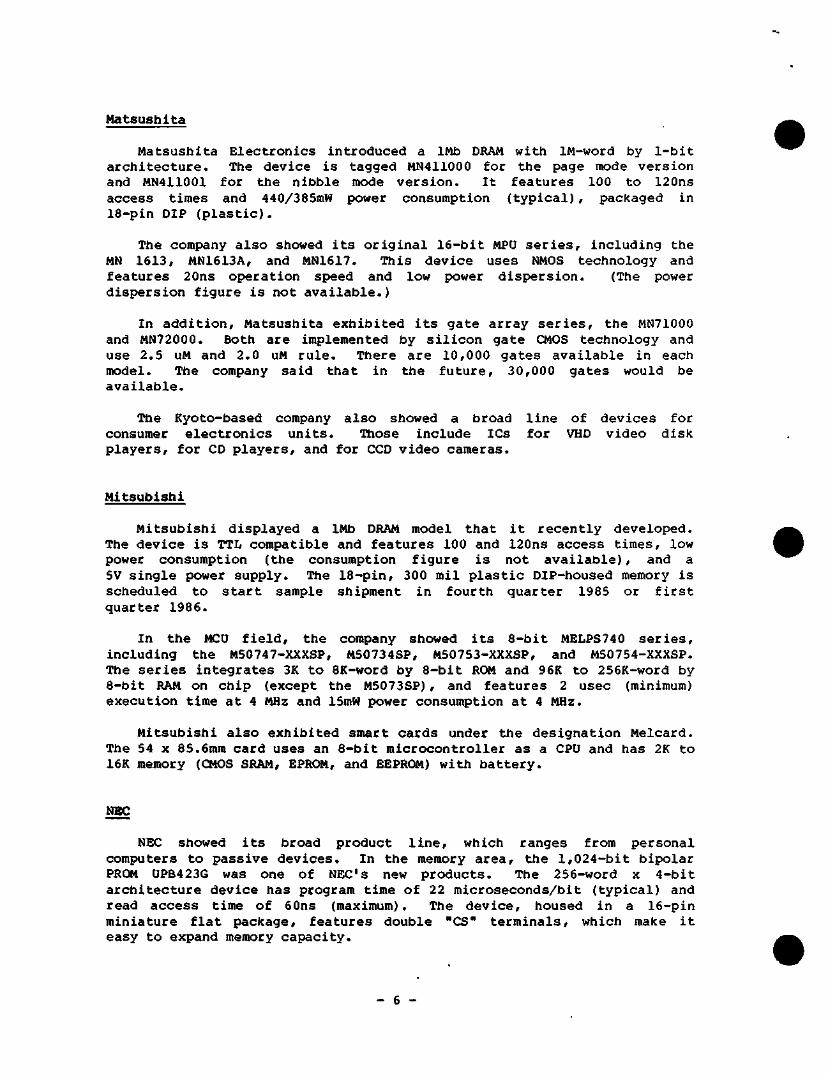
Matsushita
Matsushita Electronics introduced a 1Mb DRAM with IM-word by 1-bit architecture. The device is tagged MN411000 for the page mode version and MN411001 for the nibble mode version. It features 100 to 120ns access times and 440/385mW power consumption (typical) , packaged in 18-pin DIP (plastic).
The company also showed its original 16-bit MPU series, including the MN 1613, MN1613A, and MN1617. This device uses NMOS technology and features 20ns operation speed and low power dispersion. (The power dispersion figure is not available.)
In addition, Matsushita exhibited its gate array series, the MN71000 and MN72000. Both are implemented by silicon gate CMOS technology and use 2.5 uM and 2.0 uM rule. There are 10,000 gates available in each model. The company said that in the future, 30,000 gates would be available.
The Kyoto-based company also showed a broad line of devices for consumer electronics units. Those include ICs for VHD video disk players, for CD players, and for CCD video cameras.
Mitsubishi
Mitsubishi displayed a 1Mb DRAM model that it recently developed. The device is TTL compatible and features 100 and 120ns access times, low power consumption (the consumption figure is not available), and a 5V single power supply. The 18-pin, 300 mil plastic DIP-housed memory is scheduled to start sample shipment in fourth quarter 1985 or first quarter 1986.
In the MCU field, the company showed its 8-bit MELPS740 series, including the M50747-XXXSP, M50734SP, M50753-XXXSP, and M50754-XXXSP. The series integrates 3K to 8K-word by 8-bit ROM and 96K to 256K-word by 8-bit RAM on chip (except the M5073SP) , and features 2 usee (minimum) execution time at 4 MHz and ISmW power consumption at 4 MHz.
Mitsubishi also exhibited smart cards under the designation Melcard. The 54 X 85.6mm card uses an 8-bit microcontroller as a CPU and has 2K to 16K memory (CMOS SRAM, EPROM, and EEPROM) with battery.
NBC
NEC showed its broad product line, which ranges from personal computers to passive devices. In the memory area, the 1,024-bit bipolar PROM UPB423G was one of NEC's new products. The 256-word x 4-bit architecture device has program time of 22 microseconds/bit (typical) and read access time of 60ns (maximum). The device, housed in a 16-pin miniature flat package, features double "OS" terminals, which make it easy to expand memory capacity.
- 6 -
NEC also displayed several specialty devices designed for graphic processes, including an image-pipelined processor, the UPD7281D, and a 256K dual-port RAM, the UPD41264C. The UPD41264C has a dual-port architecture consisting of a 64K-word by 4-bit RAM port with 120ns and 150ns access times and a 256K-word by 4-bit serial access port with 40ns and 60ns serial read cycle times.
In the gate array area, the company demonstrated its CMOS-4/4A and TTL-2A/3 gate array families with design processes based on the PC-9801 series and ACOS engineering workstations.
OIci Electric
Oki Electric showed a 1Mb DRAM tagged MSM41000. The device is implemented by N-channel silicon gate technology and features 1,048,576-word by 1-bit architecture. It uses a 5V single power supply and the inputs are TTL compatible. Access time is 90ns.
Other devices displayed were: a 2K x 8-bit EEPROM, the MSM2816A AS/RS; voice-synthesized LSI with ROM, the MSM6243; solid-state recording LSI, the MSM6258; and a semiconductor laser, the OL1305/1205, which has 65mW maximum output and 1.2 to 1.3 uM oscillation wavelength.
Oki also demonstrated a smart card plus a system to read and write into the card. The Oki IC card reader and writer system has 1,200 to 9,600 Bits/sec transfer speed through a RS-232-C start/stop synchronous interface.
TDstiiba
Toshiba introduced its 1Mb CMOS DRAMs, the TC511000C-10 and 12 and TCllOOlC-10 and 12. The company has already announced plans to start l-million-per-month production of the 1Mb DRAMs in April 1986 at its Oita plant. Toshiba's 1Mb DRAMs have 1,048,576 x 1 architecture and access times of 100 and 120ns.
A new CMOS gate array series, the TC18G/19G, was also exhibited. The TC19G series has 3,200 to 10,000 gates and applies 1.5 uM design rule with features of 1.0 ns/gate. The company will start taking orders in the first quarter of 1986. A new series with up to 47,000 gates is under development and will be introduced as the TCllSG series in 1986.
Toshiba displayed a variety of microwave semiconductors such as semiconductor diodes, low-noise GaAs PETs, power GaAs FETs, and bipolar power transistors. Among them, a high electron mobility transistor, the S8900, was introduced as being under development. The device achieves ultra-low noise figures of l.SdB at F = 18 GHz and 2.4dB at F = 30 GHz.
- 7 -
DATAQDEST CONCLUSIONS
We believe that 1Mb DRAM development in Japan is clearly under way and that the marketplace will see volume shipments by 1987.
Further, there is a strong feeling in Japan that the IC card and its reader/writer system will be another huge consumer market opportunity.
Nagayoshi Nakano Gene Norrett
- 8 -
Dataquest JAPANESE — RESEARCH NEWSLETTER
JSIS Code: JSIA Newsletters
PRELIMINARY 1985 JAPANESE COMPANY MARKET SHARE ESTIMATES
SUMMARY
In the worldwide semiconductor industry's most dismal year on record, Japanese-based semiconductor companies performed significantly better than the world market. While the top 50 companies worldwide experienced a revenue decrease of 16 percent, the Japanese companies' semiconductor revenues declined only 12 percent. In the extremely depressed MOS integrated circuit market, Japanese companies' revenues were down 19 percent. This year, the linear IC market was the place to be, and Japanese companies' linear sales were up 5 percent, the only major product category where there were gains.
TOTAL SEMICONDUCTOR
Table 1 shows worldwide total semiconductor sales and worldwide rankings of the top 14 Japanese semiconductor manufacturers. NEC this year became the first Japanese company to be ranked number one worldwide in total semiconductor revenues, with sales of $1,984 million; the company was ranked third in 1984.
Five Japanese companies are in the top ten worldwide, and nine are in the top twenty. The company suffering the greatest decline was Mitsubishi, which paid this year for the tremendous gains it had made in MOS memory in 1983 and 1984.
Overall, Japanese companies gained 2 percentage points of market share worldwide, increasing from 40 percent of the total market in 1984 to 42 percent in 1985. Figure 1 shows the estimated geographic split of Japanese-based companies' total semiconductor sales in 1985. The largest portion of sales, 72.9 percent, were in Japan, 12.9 percent were in the United States, 5.3 percent were in Europe, and 8.9 percent were in Rest of World countries.
© 1985 Dataquest Incorporated Dec. 31 ed.-Reproduction Prohibited
The content of this report represents our interpretaion and analysis of information generally available to the public or released by responsible individuals in the subject companies, but is not guaranteed as to accuracy or completeness. It does not contain material provided to us in confidence by our clients Individual companies reported on and analyzed by DATAQUEST, may be clients of this and/or other DATAQUEST services This information is not furnished in connection with a sale or offer to sell securities or in connection with the solicitation of an offer to buy securities This firm and its parent and/or their officers, stockholders, or members of their families may, from time to time, have a long or short
Azabu Heights, Suite 711, 1-5-10 Roppongi, Minato-ku, Tokyo 106, Japan 1290 Bidder Pari< Drive / San Jose, CA 95131 / (408) 971-9000 / Telex 171973
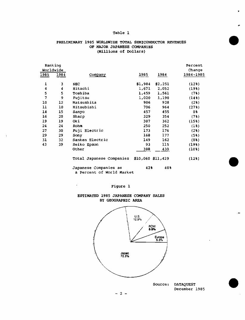
Table 1
PRELIMINARY 1985 WORLDWIDE TOTAL SEMICONDUCTOR REVENUES OF MAJOR JAPANESE COMPANIES
(Millions of Dollars)
Rank ing Worldwide 1985
1 4 5 7
10 11 14 16 19 24 27 29 31 43
1984
3 4 5 9
12 10 15 20 19 24 30 29 32 39
Company
NEC Hitachi Toshiba Fujitsu Matsushita Mitsubishi Sanyo Sharp Oki Rohm Fuji Electric Sony Sanken Electric Seiko Epson Other
1985 1984
Percent Change
1984-1985
$1,984 1,671 1,459 1,020 906 706 457 329 307 250 173 168 149 93
388
$2 2 1 1
,251 ,052 ,561 ,190 928 964 455 354 362 252 176 177 162 115 430
(12%) (19%) (7%) (14%) (2%) (27%)
o% (7%)
(15%) (1%) (2%) (5%) (8%)
(19%) (10%)
Total Japanese Companies $10,060 $11,429 (12%)
Japanese Companies as a Percent of World Market
42% 40%
Figure 1
ESTIMATED 1985 JAPANESE COMPANY SALES BY GEOGRAPHIC AREA
Source: DATAQUEST December 1985
- 2 -
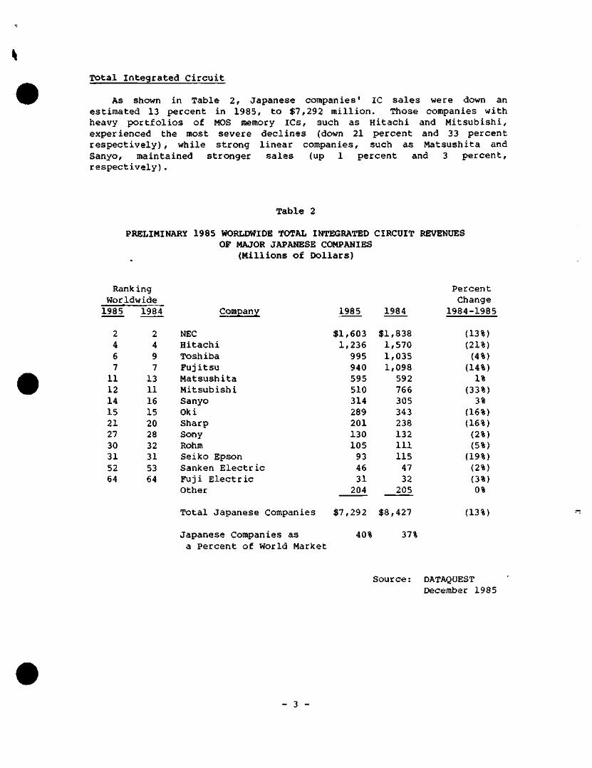
Total Integrated Circuit
As shown in Table 2, Japanese companies' IC sales were down an estimated 13 percent in 1985, to $7,292 million. Those companies with heavy portfolios of MOS memory ICs, such as Hitachi and Mitsubishi, experienced the most severe declines (down 21 percent and 33 percent respectively), while strong linear companies, such as Matsushita and Sanyo, maintained stronger sales (up 1 percent and 3 percent, respectively).
Table 2
PRELIMINARY 1985 WORLDWIDE TOTAL INTEGRATED CIRCUIT REVENUES OF MAJOR JAPANESE COMPANIES
(Millions of Dollars)
Rank ing Worldwide 1985
2 4 6 7 11 12 14 15 21 27 30 31 52 64
1984
2 4 9 7
13 11 16 15 20 28 32 31 53 64
Company
NEC Hitachi Toshiba Fujitsu Matsushita Mitsubishi Sanyo Oki Sharp Sony Rohm Seiko Epson Sanken Electric Fuji Electric Other
1985 1984
Percent Change
1984-1985
$1,603 1,236 995 940 595 510 314 289 201 130 105 93 46 31 204
$1 1 1 1
,838 ,570 ,035 ,098 592 765 305 343 238 132 111 115 47 32
205
(13%) (21%) (4%)
(14%) 1%
(33%) 3%
(16%) (16%) (2%) (5%)
(19%) (2%) (3%) 0%
Total Japanese Companies $7,292 $8,427 (13%)
Japanese Companies as a Percent of World Market
40% 37%
Source: DATAQUEST December 1985
- 3 -
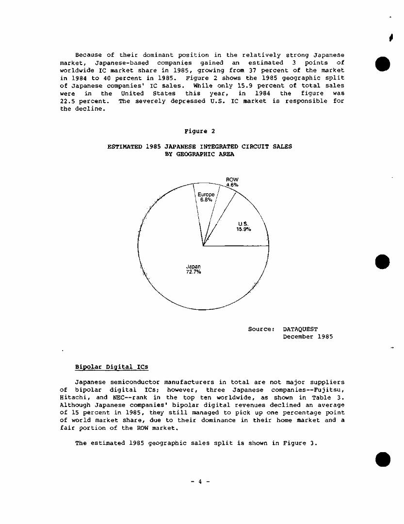
Because of their dominant position in the relatively strong Japanese market, Japanese-based companies gained an estimated 3 points of worldwide IC market share in 1985, growing from 37 percent of the market in 1984 to 40 percent in 1985. Figure 2 shows the 1985 geographic split of Japanese companies' IC sales. While only 15.9 percent of total sales were in the United States this year, in 1984 the figure was 22.5 percent. The severely depressed U.S. IC market is responsible for the decline.
Figure 2
ESTIMATED 1985 JAPANESE INTEGRATED CIRCUIT SALES BY GEOGRAPHIC AREA
ROW 4.5%
Sou r ce: DATAQUEST December 1985
Bipolar Digital ICs
Japanese semiconductor manufacturers in total are not major suppliers of bipolar digital ICs; however, three Japanese companies—Fujitsu, Hitachi, and NEC—rank in the top ten worldwide, as shown in Table 3. Although Japanese companies' bipolar digital revenues declined an average of 15 percent in 1985, they still managed to pick up one percentage point of world market share, due to their dominance in their home market and a fair portion of the ROW market.
The estimated 1985 geographic sales split is shown in Figure 3.
- 4 -
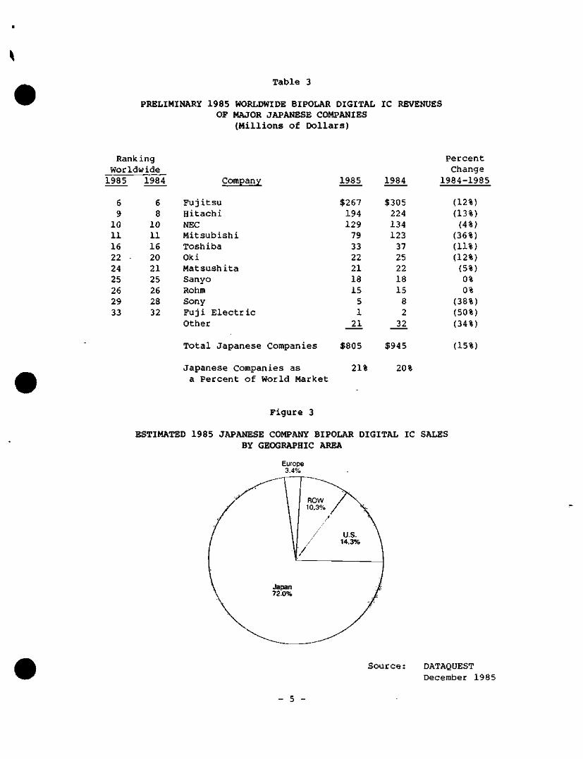
Table 3
PRELIMINARY 1985 WORLDWIDE BIPOLAR DIGITAL IC REVENUES OP MAJOR JAPANESE COMPANIES
(Millions of E>ollars}
Rank ing Worldwide 1985
6 9
10 11 16 22 24 25 26 29 33
1984
6 8
10 11 16 20 21 25 26 28 32
Company
Fujitsu Hitachi NEC Mitsubishi Toshiba Oki Matsushita Sanyo Rohm Sony Fuji Electric Other
Total Japanese Companies
Japanese Companies as a Percent of World Market
1985 1984
$267 194 129 79 33 22 21 18 15 5 1 21
$805
21%
$305 224 134 123 37 25 22 18 15 8 2 32
$945
20%
Percent Change
1984-1985
(12%) (13%) (4%)
(36%) (11%) (12%) (5%) 0% 0%
(38%) (50%) (34%)
(15%)
Figure 3
ESTIMATED 1985 JAPANESE COMPANY BIPOLAR DIGITAL IC SALES BY GEOGRAPHIC AREA
Europe 3.4%
Source: DATAQUEST December 1985
5 -
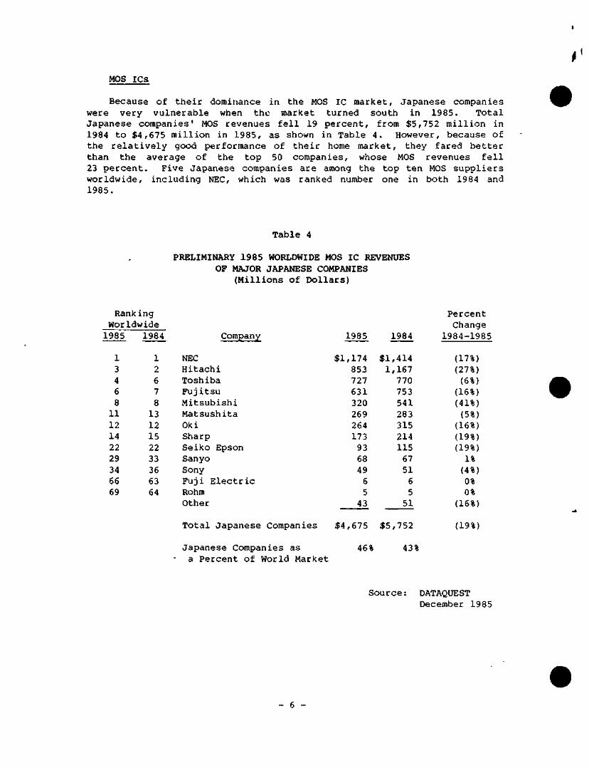
MOS ICs
Because of their dominance in the MOS IC market, Japanese companies were very vulnerable when the market turned south in 1985. Total Japanese companies' MOS revenues fell 19 percent, from $5,752 million in 1984 to $4,675 million in 1985, as shown in Table 4. However, because of the relatively good performance of their home market, they fared better than the average of the top 50 companies, whose MOS revenues fell 23 percent. Five Japanese companies are among the top ten MOS suppliers worldwide, including NEC, which was ranked number one in both 1984 and 1985.
Table 4
PRELIMINARY 1985 WORLDWIDE MOS IC REVENUES OF MAJOR JAPANESE COMPANIES
(Millions of Dollars)
Ran king Worldwide 1985
1 3 4 6 8 11 12 14 22 29 34 66 69
1984
1 2 6 7 8 13 12 15 22 33 36 63 64
Company
NEC Hitachi Toshiba Fujitsu Mitsubishi Matsushita Oki Sharp Seiko Epson Sanyo Sony Fuji Electric Rohm Other
1985
1,174 853 727 631 320 269 264 173 93 68 49 6 5 43
1984
$1,414 1,167
770 753 541 283 315 214 115 67 51 6 5 51
Percent Change
1984-1985
(17%) (27%) (6%) (16%) (41%) (5%)
(16%) (19%) (19%) 1% (4%)
o% o%
(16%)
Total Japanese Companies $4,675 $5,752 (19%)
Japanese Companies as 46% 43% a Percent of World Market
Source: DATAQUEST December 1985
- 6
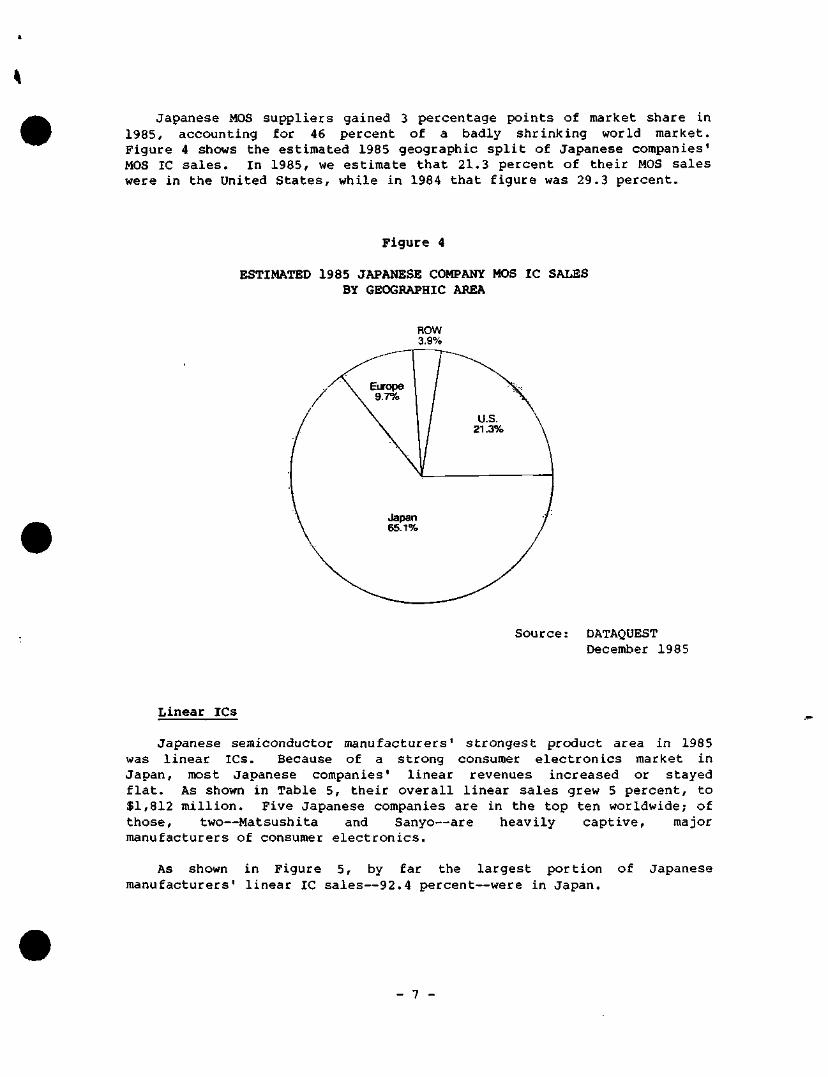
Japanese MOS suppliers gained 3 percentage points of market share in 1985, accounting for 46 percent of a badly shrinking world market. Figure 4 shows the estimated 1985 geographic split of Japanese companies' MOS IC sales. In 1985, we estimate that 21.3 percent of their MOS sales were in the United States, while in 1984 that figure was 29.3 percent.
Figure 4
ESTIMATED 1985 JAPANESE COMPANY MOS IC SALES BY GEOGRAPHIC AREA
ROW 3.9%
Source: DATAQUEST December 1985
Linear ICs
Japanese semiconductor manufacturers' strongest product area in 1985 was linear ICs. Because of a strong consumer electronics market in Japan, most Japanese companies' linear revenues increased or stayed flat. As shown in Table 5, their overall linear sales grew 5 percent, to $1,812 million. Five Japanese companies are in the top ten worldwide; of those, two—Matsushita and Sanyo—are heavily captive, major manufacturers of consumer electronics.
As shown in Figure 5, by far the largest portion manufacturers' linear IC sales—92.4 percent—were in Japan.
of Japanese
- 7 -
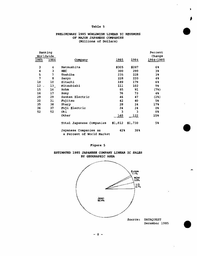
Table 5
PRELIMINARY 1985 WORLDWIDE LINEAR IC REVENUES OF MAJOR JAPANESE COMPANIES
(Millions of Dollars)
Ranking Worldwide 1985
3 4 5 7
10 12 . 15 16 29 30 35 36 52
1984
4 3 7 8
10
13. 16 ' 17 29 31 38 37 52
Company
Matsushita NEC Toshiba Sanyo Hitachi Mitsubishi Rohm Sony Sanken Electric Fujitsu Sharp Fuji Electric Oki Other
1985 1984
Percent Change
1984-1985
$305 300 235 228 189 111 85 76 46 42 28 24 3
140
$287 290 228 220 179 102 91 73 47 40 24 24 3
122
6% 3% 3% 4% 6% 9% (7%) 4% (2%) 5%
17%
o% o%
15%
Total Japanese Companies
Japanese Companies as a Percent of World Market
$1,812 $1,730
42% 38%
5%
Figure 5
ESTIMATED 1985 JAPANESE COMPANY LINEAR IC SALES BY GEOGRAPHIC AREA
Europe
Source: DATAQUEST December 1985
- 8 -
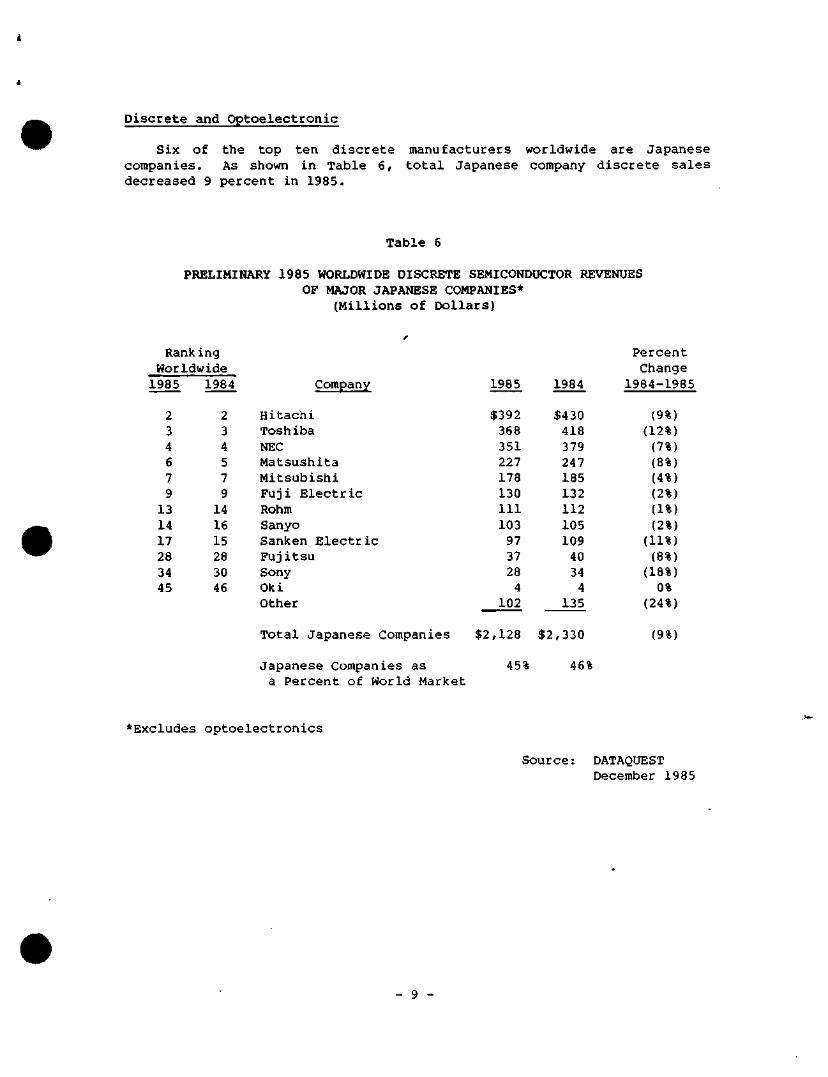
Discrete and Optoelectronic
Six of the top ten discrete manufacturers worldwide are Japanese companies. As shown in Table 6, total Japanese company discrete sales decreased 9 percent in 1985.
Table 5
PRELIMINARY 1985 WORLDWIDE DISCRETE SEMICONDUCTOR REVENUES OF MAJOR JAPANESE COMPANIES*
(Millions of Dollars)
Rank ing Worldwide 1985
2 3 4 6 7 9 13 14 17 28 34 45
1984
2 3 4 5 7 9
14 16 15 28 30 46
Company
Hitachi Toshiba NEC Matsushita Mitsubishi Fuji Electric Rohm Sanyo Sanken Electric Fujitsu Sony Oki Other
1985 1984
Percent Change
1984-1985
$392 368 351 227 178 130 111 103 97 37 28 4
102
$430 418 379 247 185 132 112 105 109 40 34 4
135
(9%) (12%) (7%) (8%) (4%) (2%) (1%) (2%) (11%) (8%)
(18%)
o% (24%)
Total Japanese Companies $2,128 $2,330 (9%)
Japanese Companies as a Percent of World Market
45% 46%
*Excludes optoelectronics
Source: DATAQUEST December 1985
- 9 -
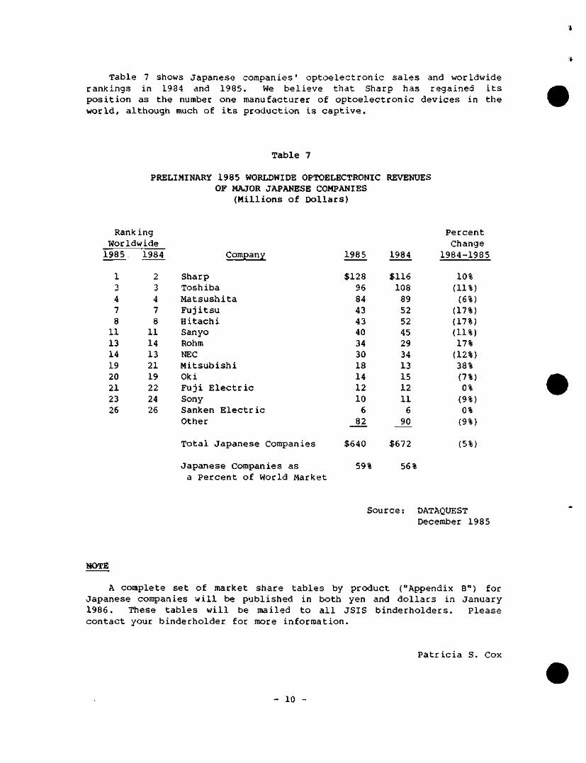
Table 7 shows Japanese companies' optoelectronic sales and worldwide rankings in 1984 and 1985. We believe that Sharp has regained its position as the number one manufacturer of optoelectronic devices in the world, although much of its production is captive.
Table 7
PRELIMINARY 1985 WORLDWIDE OPTOELECTRONIC REVENUES OF MAJOR JAPANESE COMPANIES
(Millions of Dollars)
Rank World 1985 .
1 3 4 7 8 11 13 14 19 20 21 23 26
ing wide 1984
2 3 4 7 8 11 14 13 21 19 22 24 26
Company
Sharp Toshiba Matsushita Fujitsu Hitachi Sanyo Rohm NEC Mitsubishi Oki Fuji Electric Sony Sanken Electric Other
Total Japanese Companies
Japanese Companies as a Percent of World Market
1985
$128 96 84 43 43 40 34 30 18 14 12 10 6 82
$640
59%
1984
$116 108 89 52 52 45 29 34 13 15 12 11 6 90
$672
56%
Percent Change
1984-1985
10%
(11%) (6%)
(17%) (17%) (11%) 17% (12%) 38% (7%) 0% (9%) 0% (9%)
(5%)
Source: DATAQUEST December 1985
NOTE
A complete set of market share tables by product ("Appendix B") for Japanese companies will be published in both yen and dollars in January 1986. These tables will be mailed to all JSIS binderholders. Please contact your binderholder for more information.
Patricia S. Cox
10 -
JSIS Code: JSIA Newsletters
JAPANESE INDUSTRIAL ELECTRONICS PRODUCTION TO REACH 3rll.3 TRILLION IN 1989
INTRODUCTION
The Electronics Industry Association of Japan (EIAJ) predicts in its recent report that Japanese industrial electronics production will be 5fll.3 trillion (US$54.2 billion at ¥240 per US$1) in fiscal 1989 and will achieve an overall 12.4 percent compound annual growth rate (CAGR) from 1984 to 1989. See Table 1.
The computer and computer-related products category will record the highest growth, with a 14.9 percent CAGR. The EIAJ medium-range forecast points out as the reason for this that ttiere will be raised demands for very large scale oriented computer systems and that the number of workstations connected to these systems will increase because of network expansion. The EIAJ expects production in this category to reach 5f6.0 trillion (US$25.0 billion) in fiscal 1989, which will not only represent half of the total industrial electronics production value at that time but will also be equivalent to the whole industrial electronics production value of fiscal 1984.
By product category, word processors will grow at the highest rate, with a 22.6 percent CAGR. Compared with production size in fiscal 1985, word processor production value in 1989 will be almost three times (2.8 times) larger, or ¥250 billion (US$1,042 million).
OBSERVATIONS
DATAQUEST believes that Japanese electronics production will follow the pattern of U.S. electronics production more and more and will become more oriented toward industrial products, resulting in a 10 percent annual growth rate by 1989. At the same time, consumer electronics is projected to have less than a 10 percent growth rate according to the Japan Electronics Industry Development Association.
Nagayoshi Nakano
© 1985 Dataquest Incorporated Dec. 13 ed.-Reproduction Prohibited
Inp ( onipni o' l " is repo' i 'ep'es
ifoviOed lo us in contidence by o
* i ih ihe sol ic i ianon o( an otter n
d analyzed By DATAQUEST may be c •r OATAOUEST se^v
y Qi cornjj leleness II doe:
a sale or uHer lo sell secur
oniaIn maienai jr pn connection
Dataquest Incorporated, A Subsidiary of A.C. Nielsen Company /1290 Bidder Park Drive / San Jose, CA 95131 / (40&) 971-9000 / Telex 171973
Table 1
ELECTRONICS PRODUCTION FORECAST IN JAPAN (Billions Of Yen)
Result 1984
Forecast CAGR Composition 1985 1989 1989/1984 1984 1985 1969
Industrial Electronics 6,317.9 7,067.2 11,341.3 12.4% 100.0% 100.0% 100.0%
Telecommunications Systems
Radio Communications Systems Broadcasting Equipment Radio Communications Equipment Radio Application Equipment
Electronics Application Equipment Computer and Related Equipment Others
1 , 1 9 7 . 3
6 1 2 . 1 5 9 . 6
3 7 0 . 2 1 8 2 . 3
3 , 5 7 2 . 8 2 , 9 9 3 . 6
5 7 9 . 2
1 , 3 3 3 . 4
6 3 9 . 3 6 6 . 0
3 7 6 . 9 1 9 6 . 4
4 , 0 2 2 . 4 3 , 3 6 0 . 0 3 , 3 6 0 . 0
1 , 7 9 8 . 9
9 1 2 . 7 8 9 . 3
5 4 2 . 7 2 8 0 . 5
6 , 9 7 5 . 3 6 , 0 0 0 . 0
9 7 5 . 3
8.5%
8 .3% 8.5% 8.0% 9 .0%
14.3% 14 .9% 11 .0%
19 .0%
9.7% 0.9% 5.9% 2 .9%
56 .6% 47 .4%
9 .2%
18 .9%
9.0% 0.9% 5.3% 2.8%
56 .9% 47 .5%
9.4%
15 .9%
8.0% 0.8% 4.8% 2.5%
61 .5% 52 .9%
8.6%
Electric Measuring Instrumentation 549.4 619 .2 975 .7 12.2% 8.7% 8.8% 8.6%
Electronic Business Machines Word Processors
3 8 6 . 3 9 1 . 0
4 5 2 . 9 1 3 5 . 0
6 7 8 . 7 2 5 2 . 0
11 .9% 22 .6%
6 .1% 1.4%
6.4% 1.9%
6.0% 2 .2%
Source: Electronics Industry Association of Japan DATAQUEST
- 2 -
Dataquest JAPANESE RESEARCH NEWSLETTER
JSIS Code: JSIA Newsletters
JAPANESE END MARKET ANALYSIS
SUMMARY
DATAQUEST's Japanese Semiconductor Industry Service (JSIS) has just updated its analysis of semiconductor sales by end use. We have concluded that if prices were held constant from 1984 to 1985, Japanese semiconductor consumption would increase in value by 20.8 percent. However, this is not a realistic viewpoint, due to the overcapacity problem. The actual consumption in yen value will decline by 5.2 percent. This represents a price decline of 26 percent overall (20.8 percent + 5.2 percent). For details of this actual price decline see our JSIS newsletter dated September 23, 1985, entitled "Japanese Semiconductor Market Update."
The largest Japanese semiconductor end use in 1985 is video and audio products combined, at 36.4 percent, followed by computers. The next product is digital audio disk players. These products are growing faster than VCRs and each one consumes $50 worth of semiconductors. Geographically, we have observed that Kanto is the region and Kanagawa is the specific prefecture that consumes the largest amounts of semiconductors in Japan.
JAPANESE SEMICONDUCTOR CONSUMPTION
While semiconductor consumption will be increased in 1985 by 20.8 percent at constant prices and decrease at 5.2 percent at real prices, the semiconductor industry is facing the most difficult time in its history. There are both excess capacity and significantly lower demand.
In 1984, Japanese manufacturers raised production capacity significantly, trying to meet end-user demands. However, in June 1984, semiconductor prices began to decline sharply, due to oversupply. We believe that this is still the case today.
© 1985 Dataquest Incorporated Oct. 25 ed.-Reproduction Prohibited
The content of this report represents our interpretaion and analysis of information generally available to the public or reIeased by responsible individuals in the subject companies, but is not guaranteed as to accuracy or completeness It does not contain materia) provided to us in confidence by our clients IndividuaI companies reported on and analyzed by DATAQUEST, may be clients of this and/or other DATAQUEST services This information is not furnished in connection with a sale or offer to sell securities or in connection with the solicitation of an offer to buy securities This firm and its parent and/or their officers, stockholders, or members of their families may, from time to time, have a long or short position in the securities mentioned and may sell or buy such securities
Azabu Heights, Suite 711, 1-5-10 Roppongi, Minato-ku, Tokyo 106, Japan 1290 Ridder Park Drive / San Jose, CA 95131 / (408) 971-9000 / Telex 171973
Consumer Electronics
Table 1 shows monthly Japanese semiconductor consumption classified by industry categories. Video and audio products combined have the lion's share of semiconductor consumption, controlling 38.0 percent in 1984. However, this share has decreased moderately from 41.5 percent in 1982 to 36.4 percent (forecast) in 1985 (constant price).
Japanese semiconductor consumption forms a striking contrast to U.S. semiconductor consumption, as shown in Table 2. In the United States, the data processing and communications categories have shares of 44.1 percent and 14.6 percent, respectively, while consumer electronics has only 8.0 percent. On the other hand, in Japan, the data processing and communications categories have 36.4 percent and 9.8 percent, respectively, and the consumer category has 46.5 percent. In other words, in Japan, consumer electronics ranks in the same position as industrial electronics in the United States.
Digital Audio Disk Players
In 1984, digital audio disk players had a 0.4 percent >share of total semiconductor consumption. In terms of semiconductor consumption, this figure is still low compared with VCR semiconductor consumption. We believe that the range of total semiconductors used in the disk players is $40 to $50 per unit.
DATAQUEST further estimates that monthly production of digital audio disk players will show a fivefold increase over 1984 to ¥3.3 billion in 1985.
Other Consumer Products
In Table 3, we have shown the fastest-growing end markets for semiconductors. In Table 4, we show the rankings of the major consumer products.
In Table 5, we have listed the three consumer products that are climbing the ladder of semiconductor consumption the fastest.
End Equipment Trends
Some conclusions on end equipment trends:
• We believe that the combination of the telecom market opening in Japan and the new office automation boom focused on communications will provide significant opportunity for telecom semiconductors.
- 2 -
The word processing equipment market share has increased because many Japanese makers are now supplying low-end portable versions of Japanese word processors due to a heavy demand to automate previously inefficient offices. In Japan, manufacturers of Japanese word processors that are also capable of handling Chinese characters are now estimated to control more than 80 percent of the demand in the domestic market.
Consumption by Regions
Table 6 shows estimated regional semiconductor consumption. The Kanto region has more than 50 percent share in total semiconductor consumption in Japan. The Ttokai region increased its share from 10.5 percent in 1982 to 11.8 percent in 1985. DATAQUEST expects the ratio of semiconductors consumed in the Ttokai region to continue to grow.
The average monthly semiconductor consumption in Kanagawa prefecture was 5f34.3 billion in 1984, equivalent to 20 percent of the total Japanese monthly consumption, as shown in Table 7. Che interesting observation of Table 7 is that Shizuoka prefecture's rank in semiconductor consumption grew from number 10 in 1982 to number 8 in 1984. We expect Shizuoka to move up to number 5 in 1985 as a result of the increasing importance of the manufacturing of Ando (optical communications). Brother, Nippon Automation (robots), Roland (musical instruments), Suzuki (motorcycles), Toshiba, and Yamaha.
Nagayoshi Nakano Csamu Qhtake Gene Norrett
- 3 -
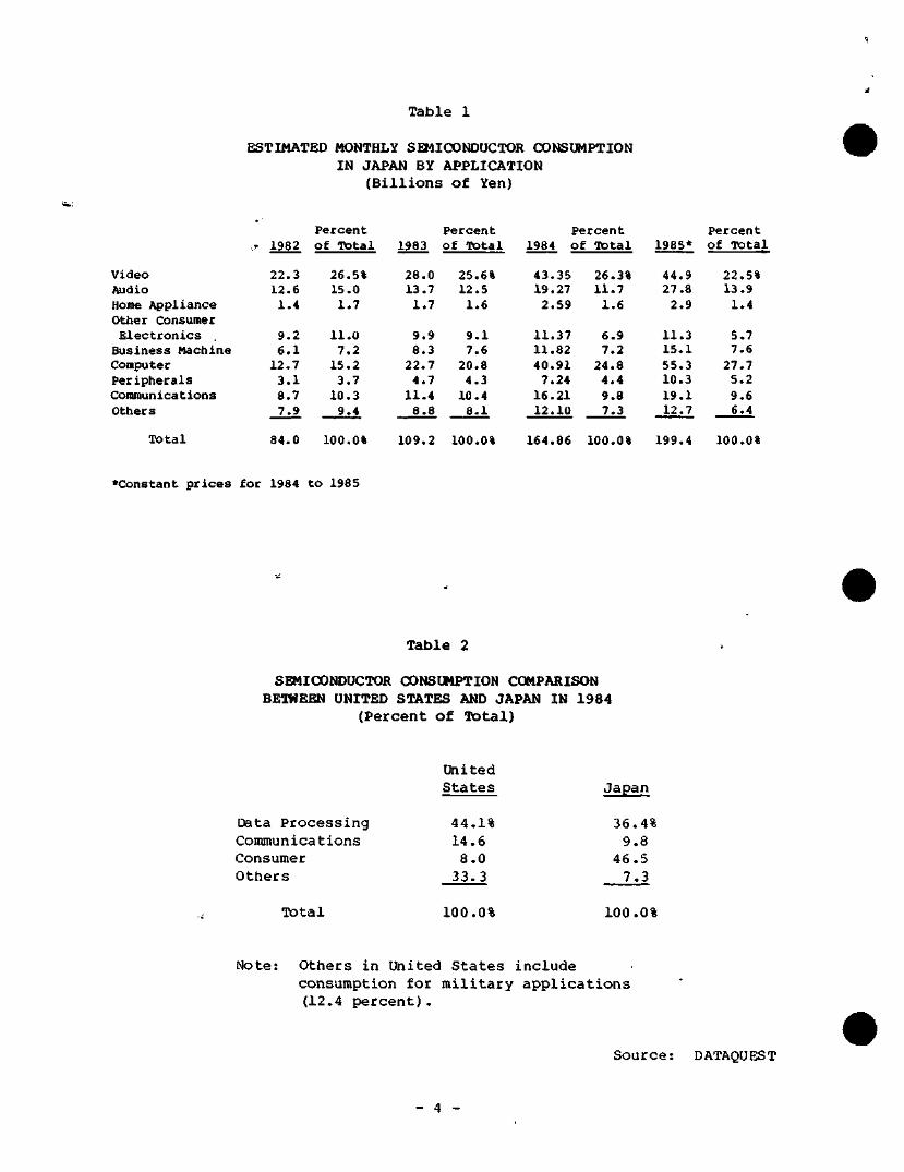
T a b l e 1
ESTIMATED MONTHLY SEMICONDUCTOR CONSUMPTION IN JAPAN BY APPLICATION
( B i l l i o n s o f Yen)
Video Audio Home App l iance Other Consumer
E l e c t r o n i c s Business Machine Computer Per iphera ls Communications Others
-• 1982
22 .3 12 .6
1 .4
9 .2 6 . 1
12 .7 3 . 1 8 .7 7.9
P e r c e n t o f To ta l
26.5% 15 .0
1.7
11 .0 7.2
15.2 3.7
10 .3 9 .4
1983
28 .0 13 .7
1.7
9 .9 8 .3
22 . 7 4 .7
11 .4 8 .8
P e r c e n t of To ta l
25.6% 12 .5
1.6
9 . 1 7 .6
20 .8 4 . 3
10.4 8 .1
P e r c e n t 1984 o f
43 .35 19.27
2 .59
11 .37 11 .82 4 0 . 9 1
7.24 16 .21 12.10
T o t a l
26.3% 1 1 . 7
1.6
6.9 7 .2
24 .8 4 .4 9.8 7 .3
1985*
44 . 9 27 .8
2 .9
11 .3 1 5 . 1 55 .3 10 .3 1 9 . 1 12 .7
P e r c e n t o f To ta l
22.5% 13 .9
1.4
5.7 7 .6
27 .7 5 .2 9.6 6.4
T o t a l 84.0 100.0% 109.2 100.0% 164.86 100.0% 199.4 100.0%
•Cons t ant p r i c e s for 1984 t o 1985
Table 2
SEMICONDUCTOR CONSUMPTION COMPARISON
BEOWEEN UNITED STATES AND JAPAN IN 1984
(Percent of Total)
D a t a P r o c e s s i n g C o m m u n i c a t i o n s C o n s u m e r o t h e r s
I J i i t e d S t a t e s
4 4 . 1 % 1 4 . 6
8 . 0 3 3 . 3
Japan
36.4%
9.8
46.5
7.3
Total 100.0% 100.0%
Note: others in United States include
consumption for military applications
(12.4 percent).
Source: DATAQUEST
- 4 -
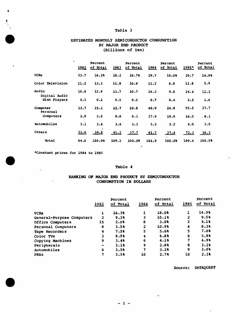
Table 3
ESTIMATED MONTHLY SEMICONDUCTOR CONSUMPTION
BY MAJOR END PRODUCT
(Billions of Yen)
Percent Percent Percent Percent 1982 of "total 1983 of Total 1984 of Total 1985* of Total
VCRs
Color T e l e v i s i o n
Audio D i g i t a l Audio
Disk P l a y e r s
Computer Persona l
Computers
Automobiles
Others
13 .7
11 .2
10 .8
0 . 1
12 .7
2 .9
3 . 1
32 .6
16.3%
13 .3
12.9
0 . 1
1 5 . 1
3.5
3.6
38 .8
18.2
11 .8
11 .7
0 . 5
22 .7
8 .8
3.6
4 1 . 2
16.7%
10 .8
10 .7
0 .5
2 0 . 8
8 . 1
3 .3
37 .7
29 .7
11 .2
16 .2
0 .7
4 0 . 9
17 .9
5 . 2
61 .7
18.0%
6 .8
9 .8
0 .4
2 4 . 8
10 .9
3.2
37 .4
29 .7
11 .8
24 .4
3 . 3
55 .2
1 6 . 5
6.0
72 .3
14.9%
5.9
12 .2
1.6
27 .7
. 8 .3
3.0
36 .3
T o t a l 84 .0 100.0% 109.2 100.0% 164.9 100.0% 199.4 100.0%
•Cons tan t p r i c e s for 1984 t o 1985
Table 4
RANKING OF MAJOR END PRODUCT BY SEMICONDUCTOR CONSUMPTION IN DOLLARS
VCRs G e n e r a l - P u r p o s e Compu ters O f f i c e Compu ters P e r s o n a l C o m p u t e r s Tape R e c o r d e r s C o l o r TVs C o p y i n g M a c h i n e s P e r i p h e r a l s A u t o m o b i l e s PBXs
1 9 8 2
1 2
15 8 4 3 9 -6 7
P e r c e n t o f T o t a l
16 .3% 9.3% 2.0% 3.5% 7.5% 8 .9% 3.4% 3.1% 3 .5% 3 .5%
1 9 8 4
1 3 8 2 5 4 6 9 7
10
P e r c e n t o f T o t a l
18 .0% 10.1%
3.0% 1 0 . 9 %
5.6% 6.8% 4 .1% 2.8% 3 .2% 2 .7%
1985
1 2 3 4 5 6 7 8 9
10
P e r c e n t o f T o t a l
14.9% 9 .5% 9.1% 8 .3% 7.0% 5.9% 4 . 9 % 3.1% 3.0% 2 .3%
Source: DATAQUEST
- 5 -
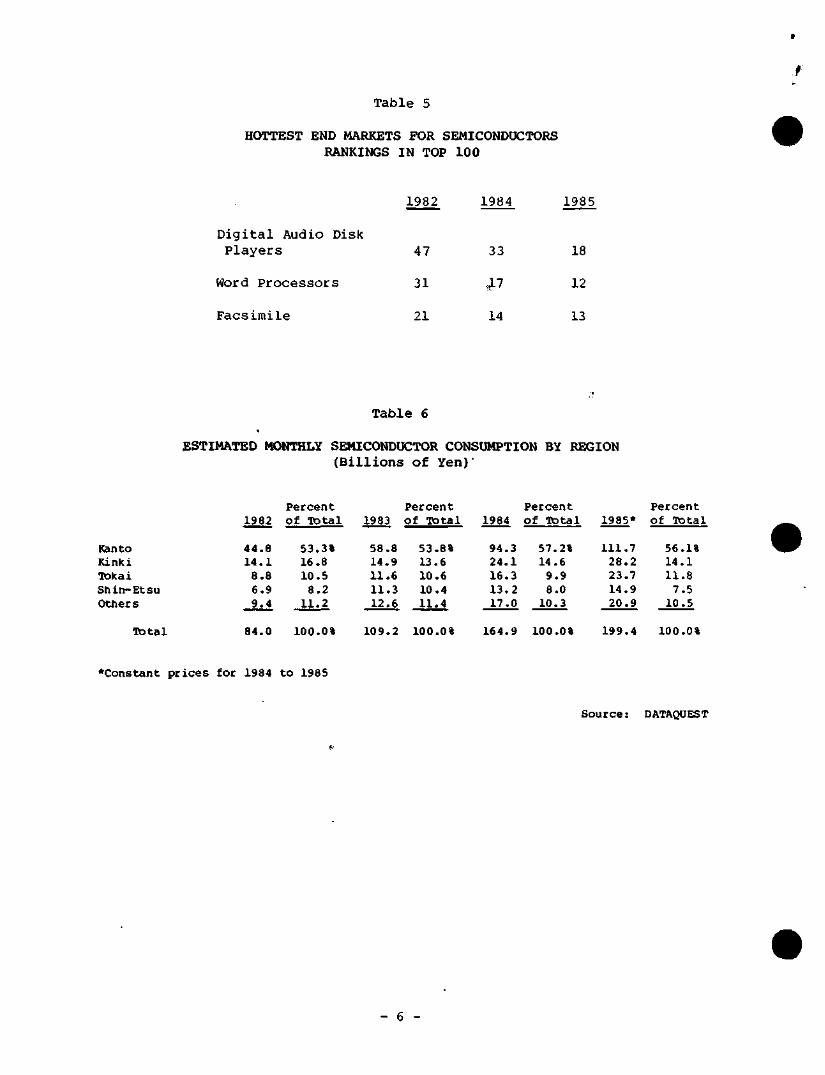
T a b l e 5
HOTTEST END MARKETS FOR SEMICONDUCTORS RANKINGS IN TOP 1 0 0
1 9 8 2 1 9 8 4 1 9 8 5
D i g i t a l A u d i o D i s k P l a y e r s
Word P r o c e s s o r s
F a c s i m i l e
47
31
21
33
:17
14
18
12
13
T a b l e 6
ESTIMATED MONTHLY SEMICONDUCTOR CONSUMPTION BY REGION ( B i l l i o n s o f Y e n ) '
Kan t o Kinki Tokai S h i n - E t s u Othe r s
I t o t a l
1982
4 4 . 8 1 4 . 1
8 .8 6 .9 9 .4
84 .0
P e r c e n t of I to t a l
53.3% 16 .8 1 0 . 5
8 .2 1 1 . 2
100.0%
1983
58 .8 14 .9 1 1 . 6 1 1 . 3 12 .6
109 .2
P e r c e n t of T o t a l
53.8% 13 .6 1 0 . 6 10 .4 11 .4
100.0%
1984
9 4 . 3 2 4 . 1 1 6 . 3 1 3 . 2 17 .0
164 .9
P e r c e n t of I to t a l
57.2% 14 .6
9 . 9 8.0
1 0 . 3
100.0%
1985*
111 .7 2 8 . 2 2 3 . 7 1 4 . 9 2 0 . 9
199 .4
P e r c e n t of T o t a l
56.1% 1 4 . 1 1 1 . 8
7 .5 1 0 . 5
100.0%
• C o n s t a n t p r i c e s for 1984 t o 1985
S o u r c e : DATAQUEST
- 6 -
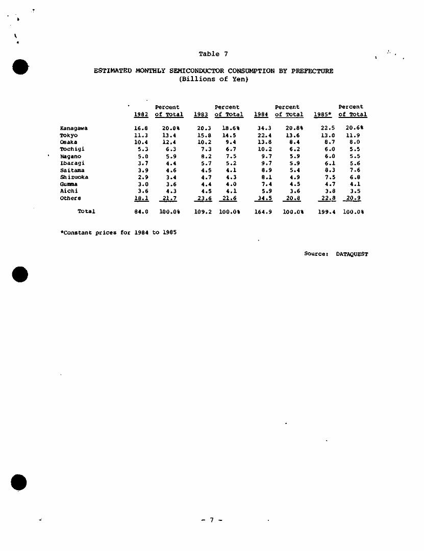
T a b l e 7
ESTIMATED MONTHLY SEMICONDUCTOR CONSUMPTION BY PREFECTURE
(Bil l ions Of Yen)
Kanagawa Tokyo Osaka Tochigi Nagano Ibaragi Saitama ShizuoKa Gumma Aichi Others
1982
16.8 11.3 10.4 5.3 5.0 3.7 3.9 2.9 3.0 3.6
18.1
Percent of Total
20.0% 13.4 12.4 6.3 5.9 4.4 4.6 3.4 3.6 4.3 21.7
1983
20.3 15.8 10.2 7.3 8.2 5,7 4.5 4.7 4.4 4.5
23.6
Percent of Total
18.6% 14.5 9.4 6.7 7.5 5.2 4.1 4.3 4.0 4.1 21.6
1984
34.3 22.4 13.8 10.2 9.7 9.7 8.9 8.1 7.4 5.9
34.5
Percent of Total
20.8% 13.6 8.4 6.2 5.9 5.9 5.4 4.9 4.5 3.6
20.8
1985*
22.5 13.0 8.7 6.0 6.0 6.1 8.3 7.5 4.7 3.8
22.8
Percent of Total
20.6% 11.9 8.0 5.5 5.5 5.6 7.6 6.8 4.1 3.5
20.9
T o t a l 84.0 100.0% 109.2 100.0% 164.9 100.0% 199.4 100.0%
• C o n s t a n t p r i c e s for 1984 t o 1985
Source: DATAQUEST
- 7
Dataquest —JAPANESE
RESEARCH NEWSLETTER
JSIA Code: Newsletters
JAPANESE CAPACITY DATA BASE SECOND UPDATE: 1984 CONSTRUCTION BOOM CREATES OVER-CAPACITY
SUMMARY
DATAQUEST's Japanese Semiconductor Industry Service staff in Tokyo recently updated the Japanese semiconductor capacity data base on new factory lines and production capacity in 1984. It appears from company announcements that Japanese and U.S. companies will bring 57 new fabs on-line in Japan from 1983 to 1987, as shown in Table 1. These figures exceed the 32 new fabs recorded in our last newsletter ("Japanese Capacity Data Base First Update," September 12, 1984). These announced factories may be stretched out due to the collapse of the demand for semiconductors. We believe that in fiscal 1985, Japanese capital spending will decline by 23 percent in yen due to the current industry downturn and over-capacity situation. Nevertheless, several companies are still planning plant expansions, especially consumer electronics manufacturers and newcomers to the industry.
RAPID PRODUCTION GAINS IN 1984
In 1984, total average monthly wafer starts increased 44.1 percent, while average monthly unit production was up 47.6 percent, as shown in Table 2. NEC remained the largest producer, but Toshiba added the most wafer capacity and Mitsubishi recorded the fastest production growth.
Oir analysis shows the following trends in 1984:
• Average monthly wafer starts grew more slowly than average monthly unit production because of the trend toward usage of larger wafers and higher productivity.
• Overall average "yield" (average monthly production divided by monthly wafer starts) varied widely, but increased for all manufacturers.
The introduction of 5-inch and 5-inch wafer lines and improved wafer processing technology accounts for the jump in monthly unit production per wafer start, especially for Hitachi and NEC. Ftor example, NEC
© 1985 Dataquest Incorporated Oct. 25 ed.-Reproduction Prohibited
The content of this report represents our interprelaton and analysis of information generally avaiIable to ihe public or released by responsible individuals in the subjecl companies, but is not guaranteed as lo accuracy or completeness li does not contain material provided to us in confidence by our clients Individual companies reported on and analyzed by DATAQUEST, may be clients of this and/or other DATAQUEST services This information is not furnished in connection with a sate or offer to sell securities or in connection with the solicitation of an offer to buy securities This firm and its parent and/or their officers, stockholders, or members of their families may, from time to time, have a long or short Dosition in the securities mentioned and may sell or buy such securities
Azabu Heights, Suite 711, 1-5-10 RoppongI, Minato-ku, Tokyo 106, Japan 1290 Ridder Park Drive / San Jose, CA 95131 / (408) 971-9000 / Telex 171973
\
produced an average of 1,800 units per wafer start in 1984, up 3 percent from 1,750 units in 1983. Althougn these ratios mask differences in product mix, wafer size, and wafer yields by production line, they provide an overall comparison of productivity trends among the top nine manufacturers.
REDUCED CAPITAL SPENDING IN FISCAL 1985
Japanese and U.S. manufacturers significantly increased their capital spending in fiscal 1984 by 101 percent I As shown in Table 3, Japanese capital spending doubled from Sf410 billion ($1.8Q billion) in fiscal 1983 to ^820 billion (33.45 billion) in 1984. DATAQUEST believes that this growtti would have been greater if bottlenecks had not occurred in semiconductor equipment production.
However, we believe that Japanese capital spending will decline 23 percent in fiscal 1985 because of excess capacity, weak demand, and growing trade friction with the United States. In March, DATAQUEST estimated that Japanese semiconductor inventory had reacned 9 percent of total domestic production. By June, we estimate that Japanese manufacturers were holding 97 million memory devices in inventory, or over 1.5 months' backlog. Further, we believe that the Japanese market will decline by 5.2 percent in yen and approximately 7 percent in dollars. (See JSIA newsletter, "Japanese Semiconductor Market Update," dated September 23, 1985.)
We also believe that U.S. consumption will be down more than 30 percent in 1985, due to a very reduced demand for PCs and small office systems for the office. We believe that underutilization of existing plants and the 24 new Japanese fabs coming on-line in 1985, 1986, and 1987 will be more than enough to handle expected demand. Furthermore, additional capacity from South Korea and Taiwan will put strong price pressure on both U.S. and Japanese manufacturers of RAMs and ASICs.
A FLURRY OF 6-INCH WAFER LINES
From our analysis, we estimate that 47 new Fab lines will have been built by U.S. and Japanese companies in Japan from 1983 to 1985, as shown in Table 1. In our data base we have captured many data points on these factories. In Table 4, we present the production operation, product manufacturer, and estimated investment amount for many of these factories. As shown in Table 5, 45 of these new lines and factories will have an investment of over sflO billion ($40 million). This very high level of investment is representative of the Japanese commitment to this industry and the very high cost of new facilities.
We believe that the shift to 6-inch wafer MOS factories is accelerating. As shown in Table 6, 10 new factories will offer 6-inch wafer processing. We believe that several more 6-inch wafer lines will be announced later this year.
-2-
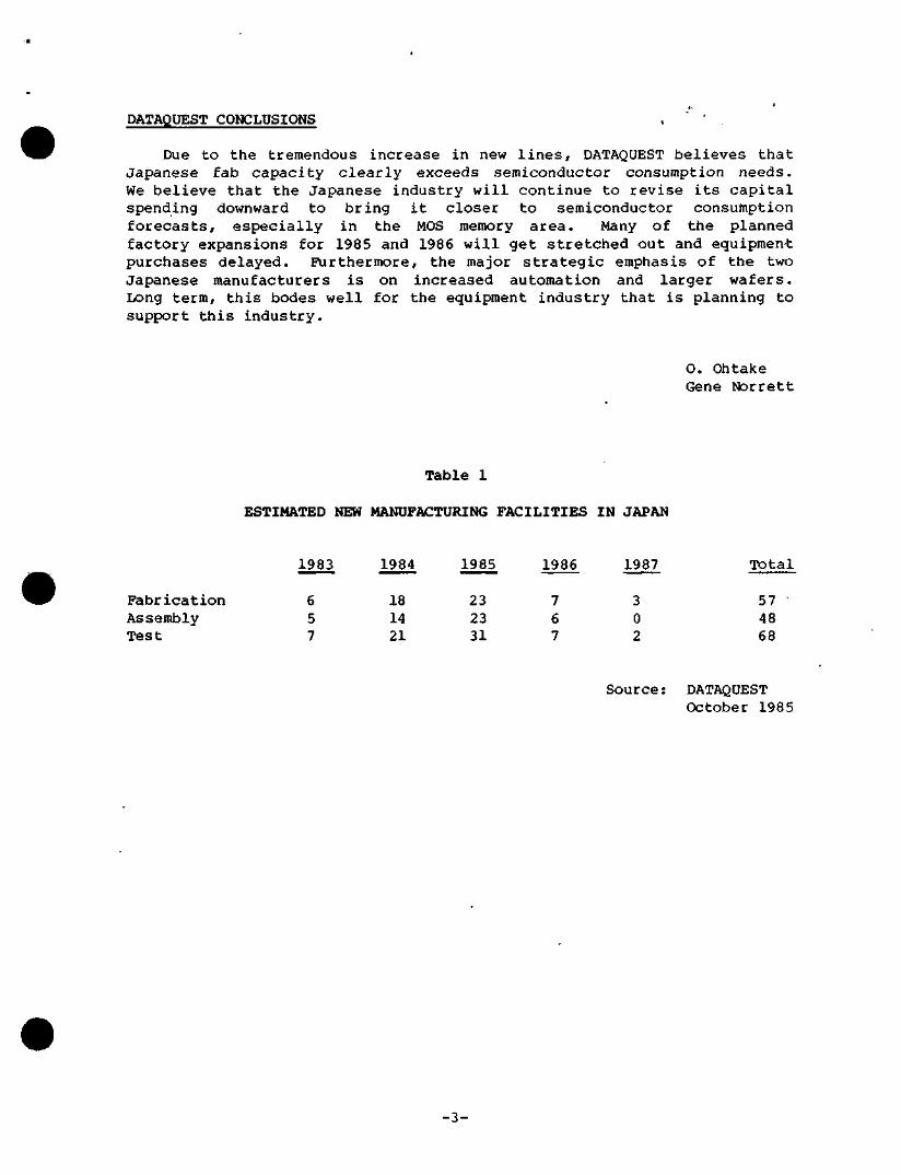
DATAQUEST CONCLUSIONS . ' '
Due to the tremendous increase in new lines, DATAQUEST believes that Japanese fab capacity clearly exceeds semiconductor consumption needs. We believe that the Japanese industry will continue to revise its capital spending downward to bring it closer to semiconductor consumption forecasts, especially in the MOS memory area. Many of the planned factory expansions for 1985 and 1986 will get stretched out and equipment purchases delayed. Furthermore, the major strategic emphasis of the two Japanese manufacturers is on increased automation and larger wafers. Long term, this bodes well for the equipment industry that is planning to support this industry.
O. Ohtake Gene Norrett
Table 1
ESTIMATED NEW MANUFACTURING FACILITIES IN JAPAN
1983 1984 1985 1986 1987 Total
Fabrication Assembly Test
6 5 7
18 14 21
23 23 31
7 6 7
3 0 2
57 48 68
Source: DATAQUEST October 1985
-3-
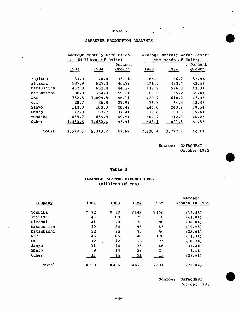
Table 2
JAPANESE PRODUCTION ANALYSIS
Average iMonthly Production (Millions of Units)
Average Monthly Wafer Starts (Thousands of Units)
Fujitsu Hitachi Matsushita Mitsubishi NEC Oki Sanyo Sharp Toshiba Other
Total
1983
33.0 587.9 452.0 96.9 752.8 20.7
114.0 42.0 438.7
1,060.6
3,598.6
1984
44.0 827.3 652.4 154.3
1,099.5 26.8 160.0 57.7 655.8
1,632.4
5,310.2
Percent Growth
33.3% 40.7% 44.3% 59.2% 46.1% 29.5% 40.4% 37.4% 49.5% 53.9%
47.6%
1983
65.3 356.2 418.9 87.0
429.7 26.9 146.0 39.6 507.7 543.1
2,620.4
1984
86.7 493.4 596.0 135.2 610.2 34.5
203.7 53.6 742.2 821.8
3,777.3
Percent Growth
32.8% 38.5% 42.3% 55.4% 42.0% 28.3% 39.5% 35.4% 46.2% 51.3%
44.1%
Source: DATAQUEST October 1985
Table 3
JAPANESE CAPITAL EXPENDITURES (Billions of Yen)
Company
Toshiba Fujitsu Hitachi Matsushita Mitsubishi NEC Oki Sanyo Sharp Other
Total
1982
¥ 32 40 41 , 10 23 48 12 11 9 13
1983
¥ 97 60 70 24 35 65 12 14 14 15
1984
¥148 125 130 95 70 140 28 35 28 21
1985
¥100 70 90 85 50 120 25 46 30 15
Percent Growth in 1985
(32.4%) (44.0%) (30.8%) (10.5%) (28.6%) (14.3%) (10.7%) 31.4% 7.1%
(28.6%)
¥239 ¥406 ¥820 ¥631 (23.0%)
Source: DATAQUEST October 1985
-4-
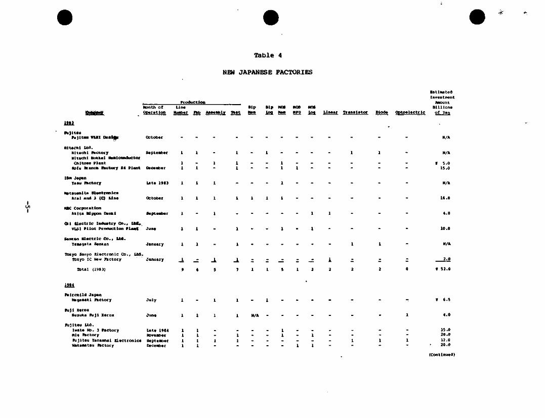
Table 4
NGN JAPANESE FACTORIES
Pcpduetlori Hontli o f Opera t ion
Line Hinbef F»b AaaaablY l » a t
Blp B l p HOB NOe HOB l o g We« WPU l o g Linear T c a n a l a t o r Diode O p t o e l e c t r l c
E a t l a a t e d I n v e s t m e n t
Anount B i l l i o n s
o f Yen
at 3 R l j l t i u
f \ i j l t a u VLSI Daalijki October N/A
I Ln I
Hltacn i Ltd, Hltaqfit m c t o r y Septeabec Hl tacn i UonIial Bes tcond i i c to t
Cnlcoae P t a n t Kotu IKancn Factory K4 P l a n t Dtceiriier
IBM Japan Yaau n c t o r y I ^ t e 1983
Hatsus t iUa U e e t c o n l c a Aral and i (C) L i n * October
Htc cocpocation Akl ta Hlppon CttnKl Septeaber
<kl E l e c t r i c Induatry O a . , LtdV VLSI P i l o t Prcmuct lon P l a n t June
Santan K lac t r lc Co . , I . td . Yaam^ata fianAan January
ToKyo Sanyo E l a c t i o n l c C o . , L M . IDKyo IC Mew n c t o c y January
Tota l (1981)
N/A
1 S.O IS.O
N/A
16 .0
4 . 0
1 0 . 0
N/A
2 . ^
T S2.a
HB«
r a i r c h l l d Japan NB9aaakl F a c t o r y
Fuj i Xerox SuxuAa F u j i Xerox
J u l y
June N/A
FVijitau Ltd . Iwate Ho. 3 F a c t o r y U t e 1984 1 1 Nla Factory Noveaber 1 1 F u j i t s u Yanaahai E l a c t r o n l c a Septeaber 1 1 Haxaaatau Factory Decenber 1 1
IS 20 12 20
.0
.0 0
.0
(Continued)
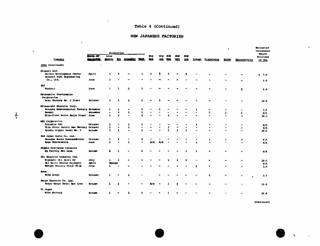
Table 4 (Continued)
NEW JAPANESE FACTORIES
CoiBpany
1984 (Continued)
NWiHi «» Production
Line iMipeer
Blp tap AaaMlJii y fiE|l^ tSS.
Blp HOB M08 HOS tog Xa* WPU Log Linear Tranalator Diode Optoelectrie
Eatlmated Investment
Amount Bi l l ions of Yen
I Oi I
Hitachi Ltd. Device Oevelopnent Center Hltacnl V[£I Engineering Co., Ltd.
MT Factory
HatBUBItlca Utct tonlcB Corporation
Aral Factory No. 4 Plant
April
June
June
October
HltekUiistil Electric Corp. FuxuoKa Beiilconductor Factory Itoveaber I^nsnl NoveiOer Klta - icas i Hocli* Sal}o Plant June
NEC corporation rukuaIila NEC October Kita Ninon Oeninl NiH factory October KyuBhu Klppon Dankl No. 7 Autuon
New Japan J!«dlo Co. Ltd. Kawaqofl Worha Senloonductor October Saga electron lea June
Nippon P[e<:lslon Circu i t ! UQ Factory New Line Autuan
Okl Electric Induatry Ltd. Nlya»t(l CKl oantt Hi July (hi Hiero Daii^n Niyaiakl April Honjyo factory Ttiicli F i l a June
Doha Roha Anagl October
Sanyo Electric Co. Ltd. IDkyo Sanyo Oenkl New Line Autuan
TI Japan Hlho Factory Autuan
Oealgn
N/A N/A
N/A
H 7.0
1.0
6.0
20.0
7.0 N/A 30.5
N/A N/A
30.0
0.8 H/A
N/A
20.0 N/A 2.0
2.5
10.0
(Continued)
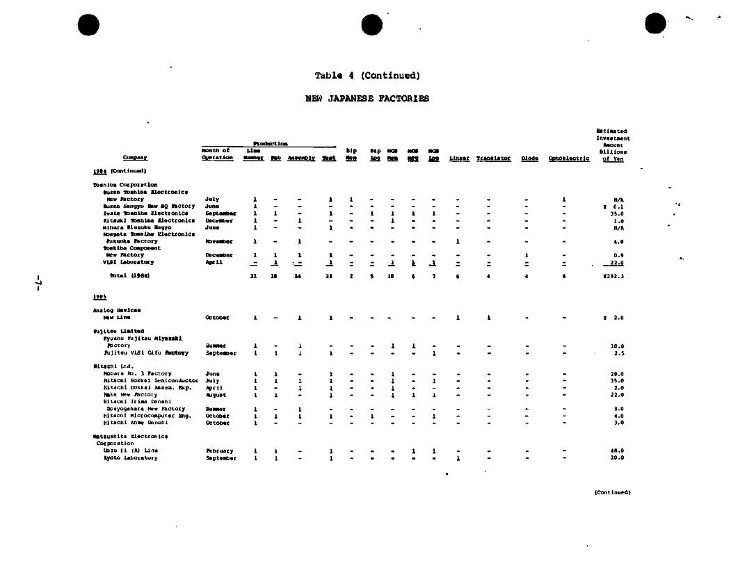
I
Table 4 (Continued)
VEH JAPANESE FACTORIBS
Prodyetioo
CcMtanV
Li»* (Continundl
^arbitia CorpQ[«tlon iuiten IbahiDa Electronlca
New FBCtoiy Buien SangyD tku HQ tectory Ivate lOBfilba CJ.«ctronic8 KitauKl 70a:iit)a Llectconica H l h a c s U n i o k u laqyo (bursts IDanlba electconlca FuKuDka factory
loaliiba Conponant WW Factory
VLSI Uboiatocy
KoLai uaa4i
Month oC Ltna Blp Opeiatton matiai nt> Aaaantily la at HCB
81p HOe lag Hca WPll l o g
Juty June £aptanbar Daceibatf J una
1 1 1 1 L
Pecanbef A ^ l l
i l U U 31
Batliuted Inveatnent
AjDount
BllXlona Linear Ttanalator Diode Optoelectrlc of Yen
H/A 0 .1
35.0 1.0 N/A
ID 7
4.0
0.9
22-0
Anal.04 Davlcaa He* Una
Rijltau Umltad Kyuanu nij i tau Hlyauki
Factory Fu}itau VUl Gifu MQtety
Ultacnl U d . NDtiaca ttj, 3 ractoiy Hitachi hoKkal SealcondtJCtot Hitachi uokttal Aaava. Sep. IBka tKn F&ctO[y ultaQtil Irlaa Denatil Ooayogahara New Factory
Hitachi Microca*E>utar Ekig. Hitachi AhB* Dsnahl
October
Sumner Septeabec
June July April Auguat
Sunner October October
1
1 1
1 1 1 1
1 1 1
-
-1
1 1 . 1
-1 -
1
1 1
-1 1 -X 1 -
1
-1
1 1 1 1
. 1 -
Matauahita ^actronica Corporation
Uiiu II IA) Una lyato Laboratory
February Septenbar
10.0 2.5
20.0 35.0
2.0 22 .0
3.0 4.0 3.0
40.0 20.0
(Continued)
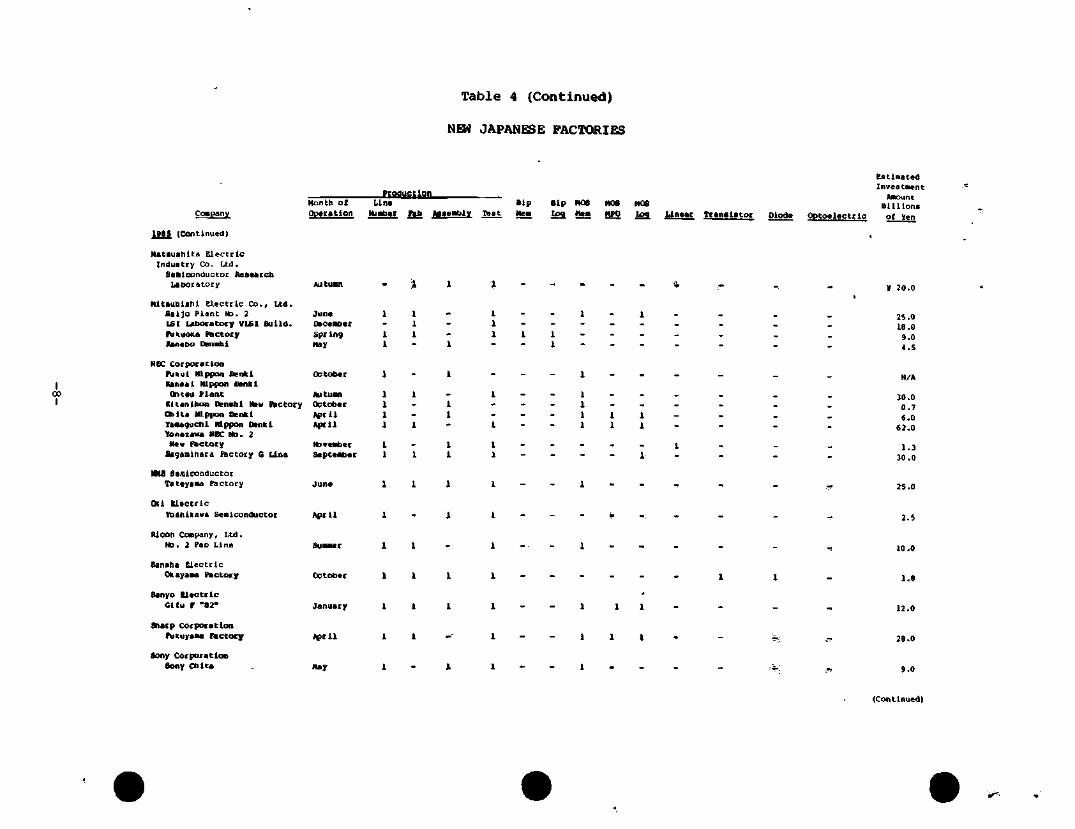
Table 4 (Continued)
NGN JAPANESE FACTORIES
I 00 I
Coapany
t»as (Continued)
Hatauahita Electr ic Industry Co. Ud .
Sanlconductof Aeaearch La<30catoiy
Mitaublanl e lectr ic Co., U d . £a i ]o Plane K>. 2 LSI Laboratory VLSI fiuild. FuItuaKa E^ctoiy Kane£)0 C^nahi
NBC corporation ftikul Nippon Oenlil Kangai IUppon DanKl
Honbh of Opatation
June OaceBbet spring May
October
Production
WtB Senicxiflductor Tateyaiaa ftctocy
Oii Electric Yoatiinaiia SeBiconductoc
Rlcon Company, Ltd. K>. 2 Pao Line
SinBha Uectc tc Ohayana factory
eanyo Electric Gltu r "82*
Snarp corporation FuJcuyaAfl Factory
Sony Corporation Sony Ctilca
April
SuuKr
October
January
i«>rll
May
Line t t i t i e r fab MaeMilv T>at
ontau Plant Kltanilion CfenaIil Naw Aictory Ot)lta Nippon DcnKi Vanagucnl Nl[^»n Denki Yonaiaua NEC Do. 2 New Factory
fiagaminara factory G Line
Autunn October April April
tbveaiber Septeober
1 1 1 1
1 1
Bip Mea
Bip MQ6 log Mea
MOS HPU
MOS Log. Unear Tranalator Diode Optoelectric
Estimated Investment
Amount Bi l l ions of Yen
25.0 18.0
9.0 4.S
M/A
30.0 0 .7 6.0
62.0
1 .3 30.0
2S.0
28 .0
9.0
(Continued)
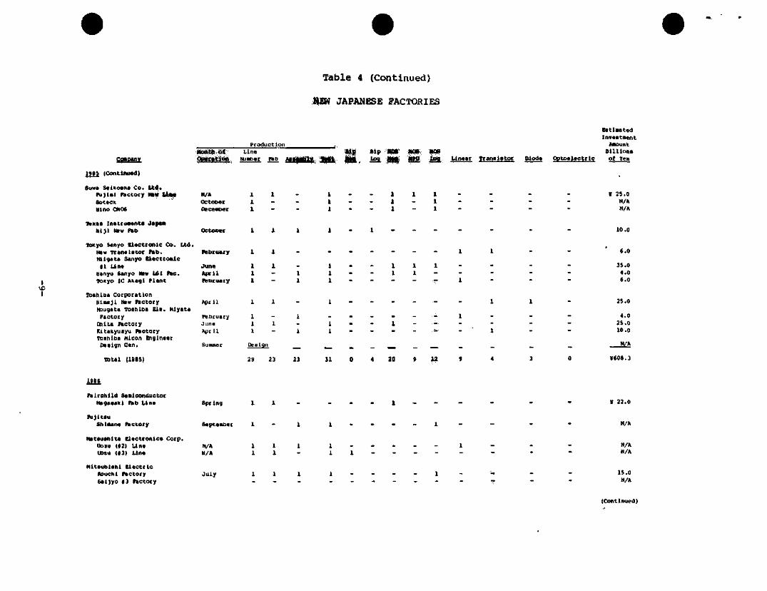
Table 4 (Continued)
HEW JAPANESE FACTORIES
I V£> I
Ceapany
I M S (Contlmiedl
Buwa s«I1[DHna Co . Ltil>
Ptoductlon •Mofiliti.iit: Line fliijteittiaft, (tiatiar ran m a ^ ^ y - iBtt..
Fu] lB l Fac tory NaW L^Ii S o t e c x d lno CMOS
Itoxaa I n a t i u B s n t a Japan t t l ] l ttow Fab
ToKyo s«nyo K l e c t c o n l c Co. L td . Hew TcanBtsco i F a b . M l g a t a Sanyo E t e c t i o n l c
11 U n e Hanyu Banyo Dm l ^ t f a c . lOKyo IC Ahagl P l a n t
Toshiba c o r p o r a t i o n t u n e j l Hen Tacto fy IC^Ligata Taahlba £ l e . K lya ta
? * c t o i y c n l t a Factocy icitakyuayu n c t o c y Toshiba Mlcon ^ g l n e e t
Des ign c « n .
N/A October QeceaiDer
OettMti
February
June Apc i l ^ b r u a r y
A p i t l
Febcuacy J una
*etn
SuBoner
1 1 I
1
1
1 1 1
1
1 1 l
Deelqn
1
--
X
I
1
--
1
-1
-
---
I
-
-1 1
-1
-1
I 1 1
1
-1 1 1
1
-1 1
,
m Bip ''«qa.' -.ttm, p p tag tltfij: "MKI. iaH.- Linear T tana ls to t plode Optee lec t t lc
Eat laated Inveatraent
Amount Billlona of Yen
V 25.0 M/A N/A
Total I19SS) } 1 20
10.0
6.0
3S.0 4.0 e.o
2S.0
4.0 2S.0 10.0
N/A
¥608.3
laas
Fa lcct i l ld SeBlconiiuctoc Kaqsaaiii Fab Line
Fuj i tsu shlaane Factozy
Hatauahita Electronica Uoiu (t2) U n e uom ( |3) Llna
Corp .
SprIng
Septeabet
N/A N/A
L
1
1 1
1
-
1 1
y 22 .0
N/A
N/A N/A
MltBublahi E l e c t r i c Kouchl Factory Sal jyo 13 Factory
Ju ly 1 1 IS .O N/A
(Continued)
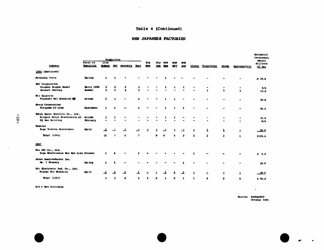
Table 4 (Continued)
NEN JAPANESE FACTORIES
o I
Eatlaated Investment
— _ fT«luetlon , ^ u „ t Month at Line B l p B i p HOS HOS HOB B i l l i o n s
Ccwwnv Opecetlon tuntiet » b A»«e»ItiIy tvtt^ MM Loa H » MPO Iga Llneet Transistor Mode Optoelectrlc pt yen
l^ti rContlnued)
Motorols IifSte Sjii Ing L I - - _ _ i _ .. . _ _ _ ,» 20.0
Nee C o r p o r a c l o n CAugoku Nippon Denlil Early 1>BS 1 1 1 1 - - 1 1 1 - . . . ^/j^ OitsuKl ^ctotjf Bumec 1 1 1 i _ - . . . _ j j j ^^^^
Ckl Electric Mlyaiejil CKl Electr ic ll^ Autunn 1 1 - 1 - - 1 1 - - . - . 20.0
aiaip Corporation FuKuyana t2 Lint Saptenbar 1 1 -• 1 - - 1 1 1 - - . _ 20.0
tbKyo Eenyo Glsctrlc Co., Ltd. Nllgata Sanyo e lectronics t2 Autumn 1 1 - - - - 1 1 - - - - . jj^o HQ (tew Bulialng February - _ . _ _ _ . . _ . . _ _ "
Toshiba Kii9< Tbehibe Blectconic ^ r l l ^ _ : _ i ^ Z Z -Z Z -Z ~ L 1 - 10.0
•total Il»a«l 10 T « 7 0 0 5 3 2 2 2 1 »135.0
1981
Hen JkC Co., Ltd. Saga Blactronica Mew tab Line October 1 1 - 1 - - - - - L - ;. _ v o . e
Ninon Sealccmiluctor Inc . No. 1 fcundty Spring 1 1 - - - - - - j . . _ _ jo.O
Ckt electronic Ind. Co . , Ltd. Hlyagi ft! e l e c t r i c April . i _ i _ l ^ Z Z -k L -L Z Z - - 30.0
total {19871 3 3 0 2 0 0 1 0 1 1 0 0 0 V 50.8
N/A - Hot Aval laU*
SourceI DATAQUEST October 19B5
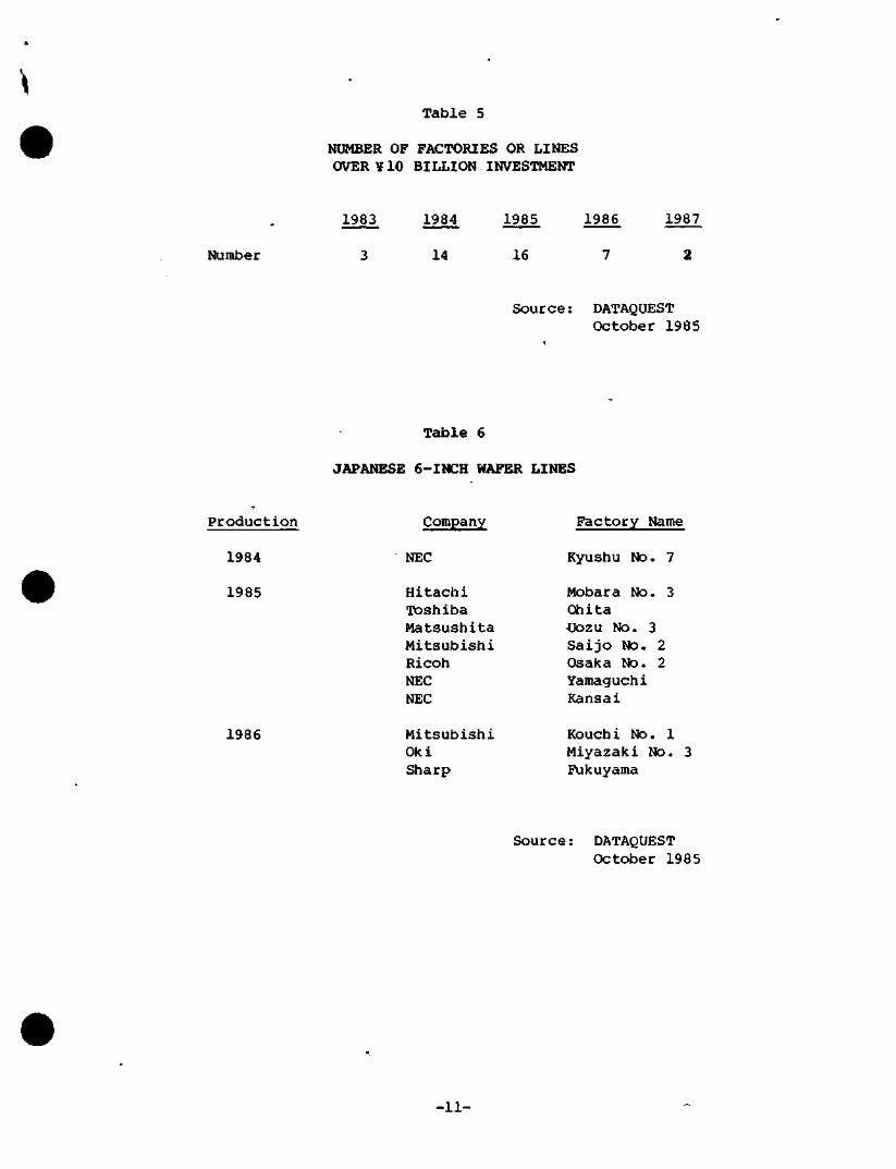
^
Table 5
NUMBER OF FACTORIES OR LINES OVER ¥10 BILLION INVESTMENT
1983 1984 1985 1986 1987
Number 14 16
Source: DATAQUEST October 1985
Table 6
JAPANESE 6-INCH WAFER LINES
Production
1984
1985
1986
Company
NEC
Hitachi Toshiba Matsushita Mitsubishi Ricoh NEC NEC
Mitsubishi Oki Sharp
Factory Name
Kyushu No. 7
Mobara No. 3 C»iita UOzu NO. 3 Saijo No. 2 Osaka No. 2 Yamaguchi Kansai
Kouch i No. 1 Miyazaki No. 3 Fukuyama
Source: DATAQUEST October 198 5
-11-
Dataquest JAPANESE RESEARCH NEWSLETTER
JSIS Code: JSIA Newsletters
JAPANESE SEMICONDUCTOR TECHNOLOGY TRENDS THIRD QUARTER 1985
SUMMARY
If 1984 was the Year of the Ox (plant investment boom), 1985 is turning out to be ttie Year of ttie Dog (R&D spending boom) in Japan. Because of the severe industry downturn, DATAQUEST observes ttiat Japanese semiconductor makers are shifting much of their capital spending to R&O spending (see Corporate R&D section of this newsletter). This R&D strategy is similar to AMD's "Liberty Chips" campaign, which is focused at developing new products. We believe that in 1985, the top Japanese semiconductor makers will spend more than 15 percent of their revenues on new researcti centers and new technologies. Ttiere are many reasons for ttiis rapid shift:
• Poor sales of existing products and excess plant capacity
• U.S. government demands for cutbacks in Japanese capital spending
• Tlie need to move up the technology ladder in light of the Semiconductor Industry Association's 301 petition to open the Japanese market and the challenge from South Korea
• The need to diversify out of the depressed memory market and prepare for the industry recovery
• The need to develop original technology due to a growing western "boycott" on technology flows to Japan
• The desire to catch up and surpass the West in microprocessors, A'SICs, and gallium arsenide (GaAs) ICs
DATAQUEST Observes that the race to develop next-generation ICs is strongly influencing device testing manufacturers. In a recent survey conducted by the Journal of Electronic Engineering, 36 percent of Japanese measuring instrument makers said they are emphasizing basic research to support new device development, including GaAs ICs, megabit 3-D memories, Josephson devices, ballistic transistors, high-speed D/A
© 1985 Dataquest Incorporated Nov. 1 ed.-Reproduction Prohibited
The content of this report represents our interpretaion and analysis of information generally availabIe to the public or reIeased by responsibIe individuals in the subject companies, but is not guaranteed as to accuracy or completeness. It does not contain material provided lo us in confidence by cur clients. Individual companies reported on and analyzed by DATAQUEST. may be clients of this and/or other DATAQUEST services This information is not furnished m connection with a sale or offer to sell securities or in connection with the solicitation of an offer to buy securities This firm and its parent and/or their officers, stockholders, or members of their families may, from time to time, have a long or short position in tne securities meniioneo ana may seii ur buy :>UI:M sui;uiiiiua.
Azabu Heights, Suite 711, 1-5-10 RoppongI, l\/linato-ku, Tokyo 106, Japan 1290 Bidder Park Drive / San Jose, CA 95131 / (408) 971-9000 / Telex 171973
themselves to prepare for ttie impact of expert systems, voice recognition and synthesis, new materials, large-capacity storage using vertical magnetization, pattern recognition, and video imaging.
DATAQUEST notes that these findings are consistent with current trends in MITI and NTT-sponsored R&D projects, wtiich are halfway toward completion. Already we see a proliferation of semiconductor lasers and optoelectronic ICs from the Optoelectronic Project (1979-1988) ; prototype 3-D ICs, GaAs, and GaAs/silicon super lattices from the New Function Elements Project (1981-1990); and prototype GaAs digital ICs, HEMT, ballistic transistors, and ECL devices from the Supercomputer Project (1981-1989) . We believe ttiat these announcements will accelerate as Japanese makers race to commercialize these experimental devices.
CORPORATE R&D LABS
As stiown in Table 1, Japanese semiconductor companies are racing to open new semiconductor R&D centers. For instance, within the last year, plans for at least 20 new research centers have been announced:
NEC announced that it will double its semiconductor R&O investment for fiscal 1985. The investment will be made in Sagamihara Works and Tamagawa works, which are NEC's centers for developing new semiconductor products. NEC researchers will focus on 32-bit MPUs for its V series, high-speed gate arrays over 20,000 gates, 1Mb and 4Mb DRAMs, large-capacity memories, and GaAs logic and memory.
Oki Electric announced that it will invest jflO billion ($46.5 million) in a new LSI research laboratory in Hachioji, a Tokyo suburb. At tihe same time, Oki has revised downward its capital spending plans for fiscal 1985 from ¥32 billion ($148.8 million) to ¥25 billion ($116.3 million), or 332.5 million less. Thus, Oki's overall capital and R&D spending will increase $14 million over fiscal 1984.
The Japan Industry Research Association announced in October that it has opened a Laser Technology Center in Chiba Prefecture. Initially financed at $1 million, the 10 researchers will conduct research in excimer lasers and other next-generation lasers for VLSI fine-line geometries (4Mb to 64Mb DRAMs). Starting in April 1986, 20 researchers will work with a 400 to 500 watt excimer laser at the center.
- 2 -
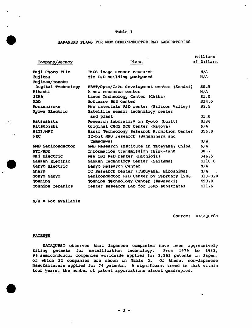
Tab le 1
JAPANESE PLANS FOR NEN SEMICONDUCTOR R&D LABORATORIES
Company/agency
R i j i P t ioto F i lm F u j i t s u F u j i t s u / T o h o k u
D i g i t a l Techno logy Hi tac t i i JIRA KDD Konis t i ico lcu Kyowa E l e c t r i c
M a t s u s t i i t a M i t s u b i s t i i MITI/MPT NEC
NMB S e m i c o n d u c t o r NTT/KDD Oki Electric Sanken Electric Sanyo Electric Sharp Tokyo Sanyo Toshiba Toshiba Ceramics
Millions Plans of Dollars
CMOS image sensor research N/A Mie R&D building postponed N/A
HEMT/Opto/GaAs development center (Sendai) $0.5 A new research center N/A Laser Technology Center (Chiba) $1.0 Software R&D center 324.0 New materials R&D center (Silicon Valley) $2.5 Satellite sensor technology center and plant $5.0 Research laboratory in Kyoto (built) $186 Original CMOS MCU Center (Nagoya) N/A Basic Technology Research Promotion Center $56.0 32-bit MPU research (Sagamihara and Tamagawa) N/A
NMB Research Institute in Tateyaraa, Chiba N/A Information transmission think-tank $0.7 New LSI R&D center (Hachioji) $46.5 Sanken Technology Center (Saitama) $116.0 Sanyo Research Center N/A IC Research Center (Fukuyama, Hiroshima) N/A Semiconductor R&D Center by February 1986 $10-$20 Toshiba Technology Center (Kawasaki) $93.0 Center Research Lab for 16Mb substrates $11.6
N/A = Not available
Source: DATAQUEST
PATENTS
DATAQUEST observes that Japanese companies have been aggressively filing patents for metallization technology. From 1979 to 1983, 96 semiconductor companies worldwide applied for 2,551 patents in Japan, Of which 32 companies are shown in Table 2. Of these, non-Japanese manufacturers applied for 74 patents. A significant trend is that within four years, the number of patent applications almost quadrupled.
- 3 -
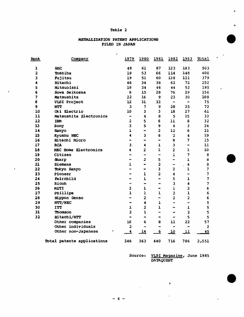
Bank
Table 2
METALLIZATION PATENT APPLICATIONS FILED IN JAPAN
Company 1979 1980 1981 1982 1983 lOtal
1 2 3 4 5 6 7 8 9 10 1 1 1 2 13 1 4 15 1 6 17 1 8 19 20 2 1 22 23 24 25 26 2 7 28 29 30 3 1 32
NEC Ibs t i iba F u j i t s u H i t a c t i i M i t s u b i s h i Suwa S e i k o s h a Matsu s t i i t a VLSI P r o j e c t NTT Oki E l e c t r i c Matsus t i i ta E l e c t r o n i c s IBM Sony Sanyo Kyustiu NBC Hitac t i i Micro RCA NEC Home E l e c t r o n i c s C i t i z e n Sharp S i emens Otokyo Sanyo P i o n e e r E a i r c t i i l d Ricot i MITI P t i i l l i p s Nippon Denso NTT/NEC ITT Thomson Hitact i i /NTT O ther companies O the r i n d i v i d u a l s O the r n o n - J a p a n e s e
T o t a l p a t e n t s a p p l i c a t i o n s
49 19 19 46 18
8 22 12
3 10
-2 3 1 4 -3 4 --1 ----2 1 --1 2 -
10 2 4
246
61 53 51 34 34 15 16 31
7 3 4 5 5 -3 -4 2 -2 --1 1 -1 1 2 4 2 1 -6 -
14
363
S o u r c e :
87 66 60 38 46 28
9 32
9 3 8 6 9 2 6 -1 1 -5 2 3 2 ---1 -1 1 --8 -6
440
VLSI
123 114 13 8
62 44 76 23
-28 18
5 11
4 12
2 8 3 2 1 --3 4 5 3 1 2 2 ----
11 -
10
716
18 3 148 111
72 53 29 30
-25 27 15
8 3 6 4 7 -1 7 1
. 4 1 -1 4 2 1 2 -1 2 5
22 -
11
786
M a g a z i n e , June
503 400 379 252 195 156 10 0
75 72 61 32 32 24 2 1 19 15 1 1 10
8 8 8 7 7 7 7 6 6 6 5 5 5 5
57 2
45
2 , 5 5 1
1985 DATAQUEST
- 4 -
GOVERNMENT R&D PROJECTS
NTT's 64-Megabit DRAM Joint R&D Project
Nippon Telegraph and Telephone's (NTT) Atsugi ECL is working with Hitactii and Toshiba to build a small "synchrotron to generate soft X-rays to design sub-micron VLSls. Located at ttie Atsugi ECL in Kanagawa Prefecture, ttie ¥20 billion ($4.3 million) 5-meter-diaraeter particle accelerator will be ready in March 1988. Currently, NTT and NEC are developing submicron VLSIs using soft X-rays produced by the 10-meter-diameter synctvrotron run by the High Energy Physics National Laboratory of ttie Ministry of Education at the Tsukuba Science City. The goal is to develop 64Mb DRAMs witti 0.1- to 0.2-micron lines using soft X-rays with 5- to 10-angstrom wavelengths.
NTT's Information Network System (INS)
On September 25, Shuji Katayama, senior manager of NTT's Engineering Departiment, gave a presentation at Santa Clara's Marriott Hotel on VLSI requirements for the Information Network System, NTT's $125 billion fiber optics and satellite network. Mr. Katayama said that two key INS features will be network digitization and intelligent processing, requiring t:tie use of new VLSI devices. In particular, the following devices will be essential to ttie system:
• INS Stii-Generation Computer—Intelligent, parallel processors
• Higli-speed VLSI—4Mb DRAM and up with 100,000 transistors
• High-speed logic—GaAs ICs, Josephson junctions, and ballistic transistors
• Optical transmission—Semiconductor lasers and optoelectronic ICs
• Mobile and satellite cormnunications—GaAs microwave circuits
• Video processing—Wafer-scale integration (one screen of 64-color graphic data on a 4-inch, 1.5Mb wafer, and natural color display on four wafers recently announced at prototype level)
• Electronic switching and DIPS computer—16-bit and 32-bit MPUs
• Megabit memory processing (4/16/64Mb DRAMs)—Electron-beam etching for submicron and synchrotron optical radiation for sub-half^nicron, plus plasma deposition equipment
f Digital subscriber loop—Audio and video codecs
• Telephone circuits—Subscriber line interface circuits (SLIC) and one-chip telephone LSIs
- 5 -
Of particular interest is NTT's INS Computer, a combination of supercomputer and 5th-generation technology, whicti DATAQUEST believes is more ambitious than MITI's 5th-generation computer because of its planned link-up witti coiranunications processing equipment. Currently, the INS Computer is being developed by the Base Intelligence Research Group at NT.T's YokosuKa Electrical Communications Laboratory. According to Mr.' Katayama, the INS Computer's major tectinologies include:
• Intelligent processing technology (knowledge base, learning, knowledge acquisition, and inference machine)
• Intelligent man-machine interface (natural language processing, ) speecti recognition and synthesis, image processing, and
automatic language translation)
• Software technology (automatic software production and testing)
• Superfast circuits
MITI's Sth-Generation Computer Project
Ttie Science and Technology Agency (STA) and MITI's Agency of Industrial Science and Tectinology (AIST) announced successful development of a Japanese-to-English automatic translation system with 70 percent translation accuracy. The system runs on a Fujitsu FACQI4 M380 mainframe computer. The translation rate is 5,000 words per hour, with 3,000 programmed grammar rules and ROH-based Japanese and English 60,000-word dictionaries. Ttie dictionaries will be expanded to 100,000 words. The LISP system is being used by ttie Japanese Information Center of Science and Technology to translate scientific and tecnnical papers from ttie West. An English-to-Japanese translation system will be released next spring. DATAQUEST notes that Japanese companies, sucti as Bravice International and NEC, have already announced similar systems.
MITI Supercomputer Project (1981-1989)
Hitachi has announced a low-end supercomputer capable of 160 million floating point operations per second (MFLOPS), parallel pipe-line processing, and 32-kilobyte vector register. The S-810 Model 5 also offers 31-bit extended addressing capacity, a maximum 32-channel I/O capacity, 96-megabytes/second throughput, and a 128-megabyte maximum memory capacity. Priced at 20 percent less than the Model 10 (315 MFLOPS), the machine has a monthly rental fee of .¥40 million ($186,000) and will be shipped starting in January 1986. DATAQUEST believes that this machine signals a trend by Hitachi and other participants in MITI's Supercomputer Project to develop low-end machines and, eventually, mini-supercomputers.
- 6 -
MITI Optical Reactive Materials Project (1985-1992)
On September 17, MITI disclosed its outline for an Optical Reactive Materials R&D Project that will receive 5f6 to ¥7 billion ($28 million to $33 million) during the next eight years. MITI aims at establishing multilayer technology for photochromic material, and photochemical hall burning (PHB) material ttiat can be used fot storing 100 million to 100 billion bits per square centimeter. Prospective participants include Hitachi, Mitsubishi, and Toshiba.
NEW PROOUCOS AND OXCHNOLOGY TRENDS
Memory
Fujitsu—A CMOS 72K SRAM witti 8K x 9-bit organization (MB81C79) ; error ctieck parity in ttie 9-bit part; 1.5-micron design rule; polycide gate technology; NMOS memory cell; 660mW power consumption during operation and 83mW at standby; 28-pin DIP; 5.8 X 7.24inm chip size; 45ns part priced at ¥15,000 ($62.50) and 55ns part at ¥12,000 ($50)
A 1.7ns GaAs 4K SRAM with 600mW power consumption; faster than NTT 2ns prototype witti 900mW power consumption announced last year; for use in supercomputers
TWO 16-bit ECL RAMs witti 4Kx4-bit architecture; 1.5-micron design rule; 70,000 elements on 6.4x4.0mm chip; 15ns access time and 8ns device selection access; 1.25 and 1.08 watts power consumption during operation; 18-pin flat or DIP packages; priced at ¥15,000 ($70)
The first 512K CMOS EPROM (MBM27C512); 200/250/300ns versions; double E>olysilicon N-channel floating avalanche-injection MOS (FAMO5) construction; 64Kx8-bit organization; 165mW power consumption at 4 MHz and below 42mW at 1 MHz; 28-pin ceramic DIP and 32-point LCC packages; sample price of ¥12,000 ($55.80) for 250ns version
Two combo SRAM-EEPROM chips with 256x4-bit structure; operates like an SRAM when power is on, with BEPROM as backup memory when electricity shuts off; for use as control storage device; MBM-2212-20 witti 200ns access time; MBM-2212-25 with 250ns access time; 18-pin DIP package; sample price of ¥3,200 ($13.30); production since October
A 1Mb CMOS mask ROM (MB83100); 150ns access speed; 128x8-bit structure; 1.7-inicron design rule; 220mW power consumption during operation; 275mW in standby; 122mW power dissipation during operation; sample price ¥5,000 ($23.25); 350ns version already available
- 7 -
A CMOS 256K DRAM (MB51256) in zig-zag inline package (ZIP) and plastic lead chip carrier (PLCC) package; for 100-mil grid PC boards for DIP-chip mounting at densities 50 to 80 percent greater than DIP packages; ZIP sample devices 5f2,700 ($12.55) and PLCC version ¥3,500 ($16.30)
A 4-Mbyte bubble memory being sampled with customers; marketing during second half of 1985
Hitactii—A prototype 16Mb compound magnetic bubble memory using ion implantation to lay a garnet thin-film surface coating on a gadolinium-gallium-garnet substrate; 3.0 x 3.5mm memory cells; reverse movement prevented by permalloy elements; commercialization planned for 1986; prototype 64Mb bubble memory planned for 1988
A bubble disk file memory compatible with conventional 8-inch flexible disk systems; three configurations available (0.25MB, 0.5MB, and 1.2MB)—sample prices ¥160,000 ($667), ¥200,000 ($930), ¥260,000 ($1,210), respectively; sales since September
Two CMOS 256K SRAM samples (B162256) , one witti battery backup; 80/100/120ns access times; 28-pin plastic DIP package; pin-compatible with Hitachi's 64K SRAM
NEC—^A 2Mb CMOS mask ROM using 1.2-micron design rule; 2.4 million elements on a 6.63 x 8.42mm substrate; 250ns access time; 40mA power consumption during operation and 100 mmA at standby; 181,,072xl6-bit organization in word mode and 262,144x8-bit in byte mode; 40-pin plastic or ceramic DIP packages; pin-compatible witti 1Mb EPROM under development; priced at ¥8,000 ($33) for lots of 1,000
Nippon Denso—A 1Mb DRAM by Japan's top automotive electronics maker to enhance its electronics expertise in automotive components; no plans for commercialization
NMB Semiconductor—CMOS 25 6K DRAM sampling; 150/200ns access time; N-channel process; technology from Inmos; production at Tateyama plant in Chiba
NTT—Joint development of 64Mb DRAM using synchrotron equipment with Hitachi, Toshiba, and other makers; goal of 100Mb DRAM by ttie year 2000
Oki Electric—A 1Mb CMOS ROM with a 15mA active operating current and lOOuA standby current (MSM531000); 131,071x8-bit organization; easy interface with 80C86/88 CMOS MPU that Oki manufactures under license from Intel: 250ns access time; TTL-compatible; 28-pin plastic DIP; priced at $23 in lots of 5,000
- 8 -
A 120ns CMOS DRAM (MSM41256-12) ; fully decoded; page-mode type witti 262,144xl-bit organization; 16-pin dual in-line package; 385mW power consumption during operation and 28mW at standby; priced at 35.80 in lots of 100
Sony—A 512K EEPROM; 5-volt power supply; 32xl6-bit structure; 20mW power dissipation; ¥700 ($3.25)
Three series of Chinese character generator NMOS ROMs; 682/3755/ 3800 ctiaractec capacity; low-scan CRT method; 24x24-bit, sample price Of ¥50,000 ($230) ; low-scan method 16xl6-bit; ¥20,000 ($93); column scan mettiod 24x24-bit, ¥30,000 ($140), low-scan CRT display with 350ns access time; 1Mb mask ROM; ceramic 28-pin DIP; column scan with 250ns access time; 1.2Mb mask ROM; ceramic 40-pin DIP
Suwa Seikosha—3 CMOS 1Mb mask ROMs; a 450ns asynchronous static device (SMM23100C) in 280-pin plastic DIP; a 250ns device (SMM63100C) in 28-pin plastic DIP; and a 450ns synchronous device in 40-pin package
Two CMOS 64K EPROMs; 100/150ns access time; 28-pin glass window ceramic package
Toshiba/Siemens—Technical agreement to jointly develop and manufacture Toshiba's 1Mb CMOS DRAM; Siemens to build a new plant in fall of 1985 and sample 1Mb DRAMs by 1:he summer of 1986
itt>Plication-Specific Memory (ASM)
• Dai Nippon—A 2Mb ROM optical card on a standard plastic card with dimensions of 85.5 x 54 x 0.75mm; first layer printed on a photosensitive surface from a master mask; light-reflective area for the second layer; CCD image sensor reader; 422K memory cards priced at ¥200 to ¥400 ($80 to $1.25)
• Hitachi-Maxell—IC cards with EPROMs and EEPROMs for banking and financial institutions, distributors, medical warehouses, and government agencies; EE-64 IC card with 64K EEPROM priced at ¥15,000 ($62.50); EP-1 64K ROM IC card priced at ¥12,000 ($50); EP-2 256K EPROM priced at ¥15,000 ($62.50); MR-Ol card reader-writer priced at ¥50,000 ($208) ; MR-121 card reader-writer with 10-key entry priced at ¥90,000 ($375)
• Toshiba—A VHS VTR witJi a built-in digital memory circuit; four 256K DRAMS and two 64K DRAMs; VTR priced at ¥169,800 ($790)
- 9 -
Microprocessors/Microcontroller ,,
• Hitachi/Mitsubisni—32-bit MPU joint development through Tokyo Uhiversity's TRON Project headed by Professor Ken Sakamura; goal Of commercializing devices by 1987
• Hitachi—TWO flexible disk drive controllers; HA16656M with a read data reproduction IC and gate signal-generation circuits; HA16652P/MP with a read-write amplification IC; sample prices of ¥2,000 ($8.37) and ¥1,500 ($6.30)
Joint development of CMOS 16/32-bit MPU with Motorola (68HC000) sampling from November; 8/10/12.5MHz versions; ceramic 64-pin DIP; 68-pin PGA; lOOmW power dissipation; SOOmw for 12.5 MHz version; 68-pin PLCC; 64-pin DIP plastic from 1986
A CMOS 16/32-bit 68000 MPU jointly developed with Motorola (68HC000); 8/10/12.5 MHz speeds; 2-micron geometry; lOOmW standard and 200mW maximum at 12.5MHz operating speed; 64-pin DIP and 68-pin pin grid array; 68-pin PLCC and 64-pin plastic DIP available from first quarter 1986
IVo fluorescent display controllers using a semi-isolation pattern process titiat puts a high-resistance transistor on epitaxial layer and a high-speed, bipolar transistor on thin epitaxial layer; anode and grid driver each priced at ¥5,000 ($23); 5-MHz logic circuit with 150V voltage
• Matsushita—A higti-performance, bit-map CRT controller (MN8356) ttiat has 64K CMOS RAM for high-speed transfer of picture data at 20ns per dot (monochrome) and 500ns (16-bit color gradation) ; 2-layer, 2^nicron CMOS silicon-on-aluminum; 85,000 transistors; 98mm square device; 84-pin flat package; sample price of ¥20,000 ($93)
• Mitsubishi—A multifunction CMOS controller for video and television remote controls {M50461-SP); lKx8-bit ROM, 32x4-bit RAM; 3 nanowatt power consumption; 2.2 to 5.5V operating voltage at 37.9 kHz to 40 kHz; 30-pin shrink-DIP package; sample price Of ¥350 ($1.65)
• A one-chip read-write logic controller for flexible disk drives (M52810EP) using a bi-CMOS process; bipolar read-write analog circuits and CMOS digital logic control circuits; 5V or 5V/12V power supply; standard I/O for 3.5-inch drives
An MCU for VTR and television remote control signals (M50460-P); 500x8-bit ROM, 16x4-bit RAM; sampling at ¥350 ($1.60)
• NEC—A high-speed CMOS interface IC (uPD4701C) for optical mouse data entry and control devices; three switch inputs; data exchange between central processor and peripheral terminal on a CPU-compatible, 8-bit data bus; lOmW power consumption during operation and 250mW at standby
- 10 -
V Series MPUs being sold in Akihabara area in lOkyo at 30 to 40 percent lower prices than Intel products; 16-bit uPD70116-8 (V30) priced at y3,400 to ¥4,000 (315.80 to $18.60); 8-bit UPD70108-8 (V20) priced at ¥3,000 to ¥3,600 ($13.95 to $16.75)
• Sharp—Two CMOS 8-bit single-chip MCUs (SM803 and LU800V1) that - are compatible with Zilog's 28; 7.14 x 5.74mm chip size; 1.5 microsecond minimum command execution time; 4K mask ROM, 6OK external memory address space, 144 bits of register file and 32 I/O ports on SM803 model; 64K memory space, 144 bits, and 24 I/O ports on LU80GV1; sample price of ¥3,000 ($12.50) and ¥2,600 ($10.80), respectively, 2.0-micron rule using CMOS silicon gate process
• Sony—TWO high-speed 4-bit CMOS single-chip MCUs; built-in LCD controller/driver and eight LCD segment outputs in CXP5024; 4,096x8-bit ROM; 224x4-bit RAM; priced at ¥800 ($3.30); general-purpose model CXP5000; 224x4-bit internal RAM; 8,192x 8-bit ROM; 64-pin shrink piggy-back package; for VCRs and CD players
• Suwa Seikosha—Three CMOS 8-bit single-chip MCUs with built-in gate arrays equal to 200 three-input NAND gates; 512 bytes ROM and 16x4-bit RAM in SMC4040C; 1,024 bytes ROM, 32x4-bit RAM in SMC4050C; 24- and 28-pin DIPs; 24-pin mini-flat package
I* Two 4-bit MPUs in 9 versions (SMC6000 Series); lKxl2-bit ROM and 489x4-bit RAM (SMC6110F); 2Kx9-bit ROM and 966x4-bit RAM (SMC6120F); 122ns and 244ns; 60-pin and 80-pin flat packages; priced at ¥360
• Tokyo Sanyo—A high-speed one-chip MCU (IiC7980) for dot matrix displays; 640x256-bit LCD panel; lOMb/sec. data transmission
(• Toshiba—Pour CMOS serial I/O controllers that function as peripheral LSIs for Z80 MPU; I/O terminals with two channels that permit simultaneous transmission and reception; synchronous data link control that prevents interference of control and data signals and allows standard interface control; two devices in 44-pin flat package for synchronous, high-speed communication; two devices in 40-pin DIP packages for lower-speed communications; sample price of ¥2,500 ($10.40)
A CMOS voice recognition LSI using switched capacitor filter technology; sample price of ¥2,000 ($9.30)
• Toshiba—A one-chip voice recognition LSI with 4K or 16K RAM (T6658A) using switched capacitor filter technology; combines pre-processing, recognition circuits, and voice registration memory on 6mm square chip in a 67-pin package
- 11 -
Digital Signal Processor (DSP)
;#' Fujitsu—An ultra-high-speed image processing system capable of processing 30 frames per second (multistage switching network) ; capable of various image-processing applications; 32-bit 68000-based minicomputer with 16 processor modules that perform histogram computation, light-shade conversion, and image calculations
• Stiarp—A DSP LSI for use in stationary-head digital audio tape recorders; sampling in October
• Sony/Toshiba—Two DSP LSIs to provide image playback graphics for compact disk audio systems; one image processor and one for generating horizontal and vertical image synchronous signals; designed under Sony/Philips specifications; comparable to 70 conventional ICs; synchronous signal IC capable of generating signals for television broadcasting in the United States and Japan (NTSC), and in Europe (PAL)
Standard Logic
• Hitachi—Two driver LSIs for fluorescent display tubes; built-in high logic circuits; 150V resistance pressure; sample price of ¥5,000 ($23.25)
• Mitsubishi—A one-chip, read-write, logic control LSI for flexible disk drives (M52810EP) using a Bi-CMOS process; bipolar, read-write analog circuits, and CMOS digital logic-control circuits integrated on the same chip; 5V or 12V power supply
implication-Specific IC (ASIC)
• Hitachi—^Bi-CMOS gate array series; 0.8ns delay time; 603 to 2,500-gate products; orders taken starting in September
• NEC—A low-price gate array product line housed in plastic PGA packages that cost 25 percent to 40 percent less than ceramic PGA packages; 2ns 2,100 to 11,000 gate arrays and 1.4ns 2,100 and 20,000 gate arrays in 72-pin packages; 2ns 3,300 to 11,000 gate arrays and 1.4ns 3,700 to 20,000 gate arrays in 13 2-pin
' packages; 208-pin packages available by late 1985
Standard cell orders taken starting in September; 1.5-micron CMOS process; 1.4ns delay time per gate; 120 cells; 12mA buffer; RAM, ROM, bit-slice CPU, and peripheral ICs
- 12 -
Eigtit CMOS gate arrays with 1.4ns gate delay and 4.5ns output buffer delay time at 5 picoF load; 2,100/3,700/4,700/6,700/ 8,000/10,500/14,000/20,000 gate devices; development cost of ¥4.4 million ($18,300) for 2,100 gate products priced at ¥1,700 ($7.10) in lots Of 10,000
Four CMOS gate arrays featuring 1.5-micron geometry and 1.4ns delay time 320/500/1000/1500 gates; 54-pin package for 320-gate device; lOO-pin for 1,500 gate device; 31.00 per unit for 320-gate arrays in 10,000-piece lots; 36,250 development cost
• NTT Atsugi Lat>—An experimental 5,000-gate array with 165ps access time; faster than previous record of 265ps; 80ps per gate
• OKi—Pour 1.5ns CMOS gate arrays; 3100/4400/6000/8000-gate arrays in 86/102/126/148-pin paclcages, respectively; ¥6 million ($27,900) developnent cost and $9.60 unit price for 2,000 units Of 3,100-gate device; ¥8.6 million (340,000) and $9.60 unit price for 8,000-gate device in lots of 1,000
A CMOS standard cell series (MSM91000) to enter the, LSI market in October; 1.5ns, 2-micron process; 30ns standard RAM access time; up to 25,000 gates and 208 pins
• Ricoh—Pour CMOS electrically programmable logic arrays (EPLs) for programming logic cj.rcuits onto an array of EPROM memory cells; 35ns delay time; logic circuit with AND(fixed)-OR/XOR construction and three with AND-OR/XOR register construction; available in 20-pin plastic DIP and 20-pin ceramic DIP; sample prices of ¥3,000 ($14.00)
• Toshiba—fai agreement to jointly develop next-generation gate arrays ("Sea of Gates") with more than 20,000 gates using 1.5-micron process; cooperative R&D agreement to be expanded eventually to 50,Q00 and 60,000 gate arrays
Two gate arrays using CMOS silicon-on-sapphire (SOS) technology; 8,370 gate array (T7027) with 35,000 elements on a 9.84 x 9.92mm chip using 1.8-micron CMOS process; 0.75ns gate delay time; 16-word X 16-bit multiplier with 11,500 elements on a 435mm square chip using 1.8-micron CMOS pattern (T9503); 250mW power consumption; T7017 priced at ¥50,000 (3208)
CAD Systems
• Seiko Electronics—A VLSI CAD workstation (SX-8000) that runs on a VAX-II; for single users
- 13 -
Optoelectronics
Matsushita—Eleven LEDs for glass fiber optic communication links; seven GaAs LEDs in LN180 series for 0.8-micron band at 30- to 70-MHz frequency ranges; four InGaAs LEDs in LN19G series in 80- to 100-MHz frequencies for 1.3-micron, long-distance cable links
A new thin-film technology to develop 1.3-micron multiquantum well laser diode; 100-angstrom ultra-thin films raised using an improved liquid phase epitaxial growth method at 589 degrees centigrade; prototype 5-layer InGaAsP laser diode operating at a 15-milliampere threshold current
A In/InAs semiconductor laser for coherent optical communication systems; new device capable of 100,000 times the information of existing lasers; 0.9-MHz wavelength
Mitsubishi—An AlGaAs/GaAs distributed feedback single-mode laser diode with continuous beam generation; 42-milliampere ttireshold current; coherence measurement and high-quality pickup for digital audio and video disks; MBE growth method under ultra-high vacuum used; developed for government program
TWO photocouplers; 50mA corrector; 35V corrector/emitter; 5KV I/O voltage; 6-pin DIP; sampling at ¥85 ($0.40) starting in September
NEC—World's first AlGalnP 689.7nm visible light laser diode that continuously generates light at normal room temperature; developed using special air lock system for metal organic chemical vapor deposition (MOCVD) system; potential for developing SBOnm visible yellow-light laser diode; plans for commercial 630nm visible light laser diode in five years
TWO 1.5-micron photodiodes for optical fiber telecommunications; commercialization by 1990; one diode capable of transmitting 2Gb/sec for 161km; second capable of transmitting 565Mb/sec. for 204km; sample photocouplers for general use and high-speed optoelectronic communications; a GaAlAs infrared LED and silicon phototransistor on a 4.0x4.4x2.0mm package (PS2101) in a 4-pin, mini-flat package; 10-microsecond response time; sample price of ¥60 (do.28); GaAlAs LEDs with photodiode transistors on the same 7.08x7.60x3.50 substrate (PS2041/PS2042); 0.3 microsecond response time; compatible with Matsushita products
Optical Technology Joint Research Center—A new epitaxial crystal growth technique for optoelectronic ICs (OEICs) integrating laser diodes with transistors; MBE method combined with maskless focused ion beam implant method to form GaAs/ AlGaAs crystals by selectively injecting ions to form p/n layers; for use in heterostructure bipolar transistors
- 14 -
Sanyo—A new mettiod for developing higti-purity, large-diameter single crystals of silundum carbon silicon for blue LEDs (the sublimation method); silundum vaporized through high-temperature (2,300 degrees centigrade), low-pressure treatment to grow 33mm diameter single crystal ingots that could yield 10,000 LED ctiips; commercialization planned for full-color blue LED displays; blue LEDs with 7 to 8 candela brightness at 3.5 volts possible
Sharp—A photocoupler series that complies with West German VDU 0730 specifications for internal insulation; 5,000V rms insulation resistance, 2.54mm pin pitch, and 8-pin DIP package priced at ¥250 ($1.16) for PC904; PCIOO and PClOl priced at ¥200 (S0.93)
Sony—Four high-output GaAlAs isemiconductor lasers produced using MOCVD; multimode type with gain-guide taper stripes (SLD201/SLD202) with maximum light output of 20/25mW and operating wavelength of 780/820nm respectively; self-aligning, narrow-stripes (SLD203/SLD204) with maximum light output of 30/40mW and output wavelength of 780/820nm, respectively
Two CMOS charge-coupled device (CCD) time-base correctors for video equipment (CXL1003P); 680-element CCD, clock driver, auto bias circuit, and clock frequency adjustable between 6 and 14 MHz; 8-pin, dual in-line package; priced at ¥1,000 ($4.65)
Stanley Electric—An infrared LED with 15mW output; 70 to 100 times faster response time; low-cost lighting source for optical coiranunications; sample price of ¥2,000 ($9.30)
Tokyo university—A semiconductor laser for environmental sensing using a CCD line sensor
Image Sensors
Sony—Two CMOS CCD time-base correctors for video equipment; time base corrector for audio signals (CXKL1003P) with a clock driver, auto bias circuit, and 680 elements in an 8-pin dual-in-line (DIL) package; priced at ¥1,000 ($4.20); time-base corrector for video signals (CSL1004P) with 15.2 to 27.2 MHz frequency range and 680 element in 24-pin DIL; priced at ¥2,400 ($10)
Gallium Arsenide
Fujitsu—A high-electron mobility transistor (HEMT) low-noise amplifier for 20 to 30 GHz satellite communication ground relay stations; GaAs and AlGaAs heterojunction placed between a Josephson junction and GaAs device; cooled by Peltier effect to -50 degrees centigrade; 1.71dB noise index and 14 0 degree Kelvin noise temperature; 38dB gain with received power amplified 6,000 times at 200W power consumption
- 15 -
A tunneling hot electron transistor ("chirp" RHET) consisting of multi-layers of AlGaAs and GaAs; potential for Ips switching speed using tunneling effect
A 4K GaAs SRAM with 600mW power consumption; 1.7ns access time; faster than NTT 2ns prototype with 900mW power consumption announced last year; 27/000 transistors on a 5.5x3.7mm chip
A higti-output GaAs FET for the transmission amplifier of a 12-GHz (KU-band) satellite transmitter; 3-watt output and 6dB power gain, with 40 percent operating efficiency; 0.5-micron gate; gold-plated heat sink through-hole construction with airbridge electrode wiring in a nonresonant package; priced at ¥1 million ($4,650)
Institute of Industrial Technology—CMOS-type ultra-high density GaAs LSI transistor described as silicon-insulator-silicon (SIS) FET structure; 3-layer structure consisting of N layers over a layer of insulation deposited on GaAS substrate; MBE method used; theoretically possible to develop 1Mb SIS FET device with 0.6-watt power dissipation and 4Mb with 1 watt
Japan Aerospace Industry Association—GaAs semiconductor compounds to be raised on U.S. space shuttle in May 1986; space lab experiments to include raising GaAs crystals, examining the effect of bismuth dopants, forming a thin single crystal film of gallium antimony over an insulator substrate, conducting vapor growth experiments with in, Ga, and Al, raising crystals by diffusion method for optoelectronics, and melting and solidifying lead silicon; expected cost of experiments about $1.2 million
Matsushita—A GaAs Hall element with a 300-millivolt output voltage; for use as rotation controller and position sensor for VTRs and compact disk players; replacement for indium-antimony; sample price of ¥80 ($30)
Mitsubishi—A high-integration GaAs FET with 0.2-micron gate width; l.OSdB noise index at 12 GHz; mutual conductance of 170 to 180 milliseconds per millimeter; 6- to 12-dB gain; E-beam focusing improved by using 100-KeV double-charged silicon device with ion irradiation through an 0.5-micron thick mask
Three GaAs FET amplifier modules with 1.8dB gain and 2.2 to 2.4dB noise; FA12201 for business telecommunication systems and DBS in Japan; 11.7 to 12.2 GHz; priced at ¥7,500 ($34.90); FA12202 for DBS in the Uhited States and Australia (12.2 to 12.75 GHz), ¥8,000 ($37.20); FA12203 for DBS in Europe; 11.7 to 12.5 GHz, ¥8,000 (NDJ/300)
NEC—New technology to fabricate GaAs logic circuits with 3,000 gates and a 30ps delay time; commercial-quality GaAs logic at 16K reached; result of MITI's Supercomputer Project
- 16 -
•
A prototype High-speed GaAs FET capable of 602 millisiements per square millimeter at room temperature, or three times conventional FETs; reduced resistance in central electrode made witti self-aligned gate structure; silicon oxide insulator applied to walls of tungsten silicide gate
A 5ps GalnAs transistor employing a 5-atom thick AlAlAs film over a GalnAs substrate; twice the speed, of conventional GaAs; mutual conductance value 1.5 times greater than HEMT; 5ps switching speed achieved at normal room temperature (equal to Josephson device at -270 degrees centigrade); for use in developing higti-speed ICs and ultra-high-speed transistors for communications systems
Nippon Metals—Sampling 2-inch GaAs wafers starting in October; plans for 3-inch wafers in the future
Oki Electric—A "reverse HEMT" with AlGaAs and GaAs layers over AlGaAs substrate; 0.7 micron elements; 30 milli<7olts for 1,coo-element prototype
Higli-purity GaAs crystal grown on silicon substrate; experimental material being developed u'nder MITI New Functions Element Project's superlattice project
Ptiysical and Chemical Research Institute—A laser beam irradiation MOCVD process for increasing GaAs crystal epitaxial growtti by 100 times; crystal growth pattern isolated and epitaxial layer thickness controlled; semiconductor masks fabricated wititiout mask reticles; precise control of GaAlAs doping; argon laser used to irradiate substrate in a chamber filled with gas compound of trimethyl gallium, hydrogenated arsenide, and hydrogen; further work to reduce crystal width from 350 microns to several microns
Josephson Junctions
No major announcements.
Stemdard Logic
• Mitsubishi—A prototype prescaler IC using silicide-self-aligned silicide base, contact technology (SCOT); 2.1-GHz operation frequency and 56mW power consumption; 27 patents filed two years ago
- 17 -
Bipolar Digital
Fujitsu—Two 16K ECL RAMs with 4Kx4-bit structure; U-shaped isolation and 1.5-micron pattern; 70,000 elements on 6.4x4.0iiim chip; 15ns access time; 8ns device selection access; 1.25 watt (MBM10484-15) and 1.08 watt (MBM10G484-15) power consumption during operation; 18-pin flat or DIP packages; priced at 5fl5,O00 (370)
Matsustiita—Sampling advanced low-power Schottky (ALS) TTL; 4ns access time; ImW power dissipation
Mitsubishi—A pre-scaler IC ttiat can handle 2.1-GHz frequencies at 56mW with a power dissipation of 63mW; frequencies of 1.4 GHz at 30mW and 850 MHz at 19mW also handled; for use in mobile wireless systems and satellite broadcasting receivers; silicide-self-aligned silicide base, contact technology (SCOT); 27 patents filed 2 years ago; SCOT bipolar transistor with 11.5-micron wide emitter capable of reactiing 9.6-GHz cutoff frequency
TDK Corporation—Eigtit high-output, TTL delay lines; 8-pin DIP packages with Schottky TTL in a transfer-molded, resin unit; 60ns. input/output times; low-profile (5.08mm) for automatic insertion mounting
Linear/Analog
NEC—Two hybrid ICs for satellite microwave amplifiers; 15,000 times amplification of weak signals; ultrasmall earth stations with power supply equipment possible; sample price of ¥132,OOO ($614)
Rohm—A linear IC (BA1610) for frequency-shift keying for local area networks and data communications links; a transmission IC and receiving IC integrated on one chip; half-duplex send-receive capability and a phase-locked loop method to prevent operation errors; 26.3x6.5x3.4mm 20-pin DIP package
A single-chip digital servo LSI using linear CMOS process for controlling rotation and phase for VCR drums (BU2710S); 40mW power consumption; 4.5V to 6V operating voltage range
Discretes
No major announcements.
- 18 -
New Semiconductor Functions
• Ajinomoto/Tokyo institute of Technology—A prototype bioelectronic switching device (biochip) ttiat combines protein from fish eyes witti an ion-sensitive PET; silicon nitride insulating membcance coated witti porous acetyl cellulose membrane film; pores filled with a deep red, photosensitive pigment found in fish retinas (rhodopsin), combined with ptiosphatidyl choline by ultrasonic wave irradiation, and iimnobilized; lOOmW time electrical potential generated
• Fujitsu—A hot electron transistor (HET) potentially faster than a Josephson junction device; MBE method used to develop multilayer structure of GaAs/AlGaAs laid over a GaAs substrate; total of seven layers; tunneling effect employed to achieve 1.3 amplification of electrical currents
• Hitactii—A semiconductor laser 2-dimensional device simulator called Hitactii Laser Diode Engineering (HILADIE) software; capable of analyzing electron movement and laser oscillation using Hitactii's S-810 supercomputer
• MITI—High-sensitivity biosensor developed at Electrotechnical Laboratory in Tsukuba
• Tokyo University—A 3-dimensional IC using amorphous oxidized silicon; group tieaded by Professors Takagi and Ishikawa; 0.35-micron thin-film layer; ion beam and plasma CVD methods used
• Toshiba—A new 3-dimensional IC technology for 4Mb and 16Mb DRAMs; 4mm square single crystal silicon film grown on an IC substrate covered with an insulating film; goal of practical use within five years
New Processes
• Toshiba—A prototype 73-stage ring oscillator with a 49ps delay time using a 50KV electron beam generator to achieve a 0.25-micron pattern; use of proximity effect that spreads light and creates an uneven exposure over the pattern; for use in 4Mb, 16Mb, and 64Mb DRAMs
• New Metals National Research Institute—A method to produce large single-crystal tungsten from tungsten polycrystals by injecting calcium and magnesium to polycrystal tungsten powder; pressure molding and sintering at 1,850 degrees centigrade to develop compound, which is then hot-rolled into sheets and annealed at 2,500 degrees
• Toshiba Ceramics—Plans to build central research laboratory to develop silicon substrates for 16Mb DRAMs
- 19 -
Manufacturing Processes
• Toshiba—A bias exposure photolithography method to develop 0.25-micron geometries for 64Mb DRAMs
• Toshiba/Toshiba Ceramics—A high-precision, long-lasting lapidary disk to polish silicon wafers; 105cm diameter for 4-inch wafers; 120cm diameter for 5-inch wafers; priced at ¥950,000 ($4,420) per disk
• Ultrasonic Engineeering—A fully automatic gold wire bonder for hybrid ICs (UBB-7-1A); moving sphere of manipulator plus/minus 35mm in X and Y directions; 64-chip maximum pattern recognition capability; priced at 5fl5 million (369,800)
Manufacturing Equipment
• Fuji Electric—A dust counter capable of measuring 0.11-micron dust particles for 1Mb DRAM class VLSIs
• Institute of Industrial Technology—An X/Y table to detect the accuracy (within 0.01 micron) of placing a wafer mask over the wafer, using synchrotron orbital radiation (SOR) lithography; potential use for developing 0.1-raicron geometries for 256Mb DRAMS and up; greater accuracy than steppers, E-beam, and x-ray litihography that are only sufficient for up to 0.3-micron geometries
• Seiwa Sangyo—Three dust-proof clean chambers for producing and storing ICs; Class 10 level for CBS-100 and CBS-200; Class 100 for CBS-300
• Shimizu Construction—A filter system that removes 99.9 percent of the fine salt particles from air, enabling companies to build plants near the ocean; a 3-stage filtering system priced at ¥20 million ($83,000)
• Tamura—A compact automated solderer for soldering lead frames of DIP devices (EC15-42S); capable of soldering 5,200 chips per hour on a 16-pin IC
Test Equipment
• Ando Electric—A VLSI memory tester for 1.6Mb DRAMs and SRAMs (DIC8042); 40-MHz test rate with plus/minus 1.1ns timing accuracy, lOOps resolution, and lOOps strobe resolution; autohandler (AH-633) capable of measuring 16 devices at the same time
- 20 -
Anritsu Electric/Mitsui—A helium-neon laser probe (Data Probe 2010) to locate defects in logic ICs; 1.8-micron laser operating under 20 MHz without vacuum equipment to inspect chips at 18 to 25 degrees centigrade
Nihon Den-Netsu—In-circuit IC tester (NCT-12 00) with an automatic guarding system; capable of automatically inspecting for solder bridge, poor insertion of mounted parts; disconnected patterns, and short circuits; 2-second testing of short and open circuits on 320 pins
Takeda Riken—DC analyzer (T661A) to measure DC parameters of MOS devices for up to six channels ranging from O.Ol picoA to 500mA and 10 microV to 1,500V, priced at ^7.1 million ($29,600); companion system (T661A) for other devices priced at ¥10.79 million ($45,000)
Packaging
Mitsubishi Metals—A low-void solder suitable for die bonding witti a ceramic-sealed package; dissolved gases and oxides reduced to 2 to 5 parts per million
NEC—A transfer nold package for Compact Series hybrid ICs; CK24/C42/C64 devices in flat and mini-flat packages with 2.54mm and 1.778mni lead pitches
Sheridan Tatsuno
- 21 -
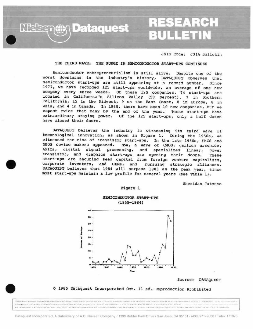
Dataquest RESEARCH BULLETIN
JSIS Code: JSIA Bulletin
THE THIRD WAVE: THE SURGE IN SEMICONDUCTOR START-UPS CONTINUES
Semiconductor entrepreneurialism is still alive. Despite one of the worst downturns in the industry's history, DATAQUEST observes that semiconductor start-ups are still appearing at a record number. Since 1977, we have recorded 125 start-ups worldwide, an average of one new company every three weeks. Of these 125 companies, 74 start-ups are located in California's Silicon Valley (59 percent), 7 in Southern California, 15 in the Midwest, 9 on the East Coast, 8 in Europe, 8 in Asia, and 4 in Canada. In 1985, there have been 10 new companies, but we expect twice that many by the end of the year. These start-ups have extraordinary staying power. Of the 125 start-ups, only a half dozen have closed their doors.
DATAQUEST believes the industry is witnessing its third wave of technological innovation, as shown in Figure 1. During the 1950s, we witnessed the rise of transistor start-ups. In the late 1960s, PMOS and NMOS device makers appeared. Now, a wave of CMOS, gallium arsenide, ASICs, digital signal processing, and specialized linear, power transistor, and graphics start-ups are opening their doors. These start-ups are securing seed capital from foreign venture capitalists, corporate investors, and OEMs, and pursuing strategic alliances. DATAQUEST believes that 1984 will surpass 1983 as the peak year, since most start-ups maintain a low profile for several years (see Table 1).
Sheridan Tatsuno Figure 1
SEMICONDUCTOR START-UPS (1955-1984)
Source: DATAQUEST
1985 Dataquest Incorporated Oct. 11 ed.-Reproduction Prohibited
Tf\e contenl of
provided 10 us
witM the so I ic i l
this report represents out
, c o n N a e n c e b y o u - n , e n ,
a t i o n o l a n o H e r I o h u v s e
interpreial ion and analysis ol mlormal ion
ioOi>'iGuai compan.eH reponeo or ana ana
unties fh is f i rm and ils parent and/o- Ihe
genetaHy available lo 1
yzed Dy DATAQUEST
o'l^cers stocKhoide-s
ie puDhc or
i>dy be c|.(;n
or rnen^tipr
eleasp
s o i r
of -he
] by 'espo
sand. 'o-o
- families
siDle individuals in Ihe su
her DATAQUEST services
Tiay t-om lime lo hr,ie hav
l e c
T h .
e a
companies Ou
,r.Io-mat.on,s
)ng or ShOM pOS
i s n
l ion
1 guarjr
r^.shed
n I h . s e
leedas
cunl ies
l o a
m e
ccura
none
,y or comple leneis Iji4^pMt nL|1._i;ntitl|i11 TTrfLLAf'tl
.• j i ' F I i r ;»* I I 1(1 f Ij I ITIrr T r .T rirTunf^rnnf
d a n d m j . sell o , b u , such „ c u n „ «
Dataquest Incorporated, A Subsidiary of A.C Nielsen Company / 1290 Bidder Park Drive / San Jose, CA 95131 / (408) 971-9000 / Telex 171973
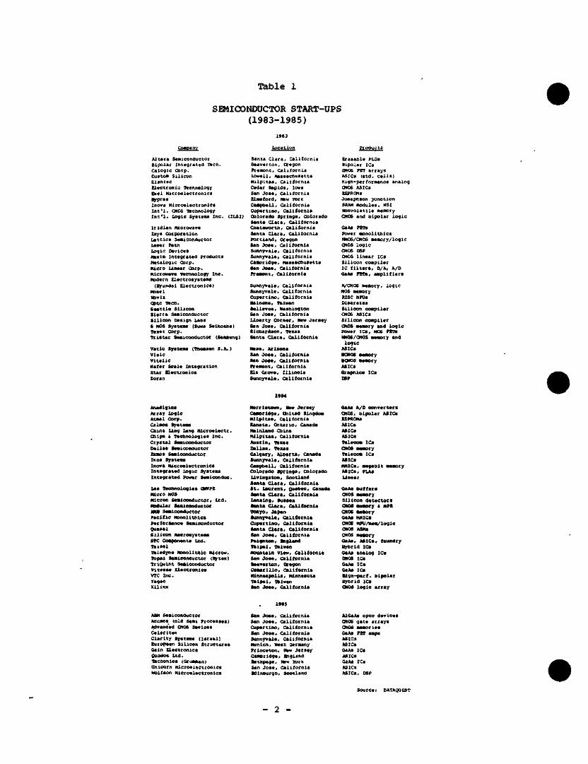
Table 1
SEMICONDUCTOR START-UPS (1983-1985)
Conpany
A l t e r a Semiconductor B i p o l a r I n t e g r a t e d Ttecti. C a l o g i c Corp . Custom S i l i c o n E l a n t e c E l e c t r o n i c n c n n o l o g y Bxe l H i c r o e l e c t r o n i c B Hypres Znova H i c r o c l e c t r o n i c s I n t ' l . atOS iftcftno logy I n t ' l . Log ic Sys tems I n c . (ZLSI)
Irldian Hicrowave Ixya Corporation lattice Semiconductor Idser Pa til Logic Devices Haxim Integrated products Hetalogic Corp. Micro Linear Corp. Microwave netirralogy Inc. Modern Electrosystans (Hyundai Electronics)
Hosel NDvix Opto Dich. Seattle Silicon Sierra Semiconductor Silicon Design Labs 6 MOS SystCBS (Suwa Seikostia) Texet Corp. Trlatar Semiconductor (Saiuung)
Vatic Systeas (Thoaaen S.A.) Visic vitelle Hafer Scale integration
xtar Electronics Zoran
Ideation
Santa Clara, California fieaveiton, Cregon Fremont, California Lowell, Massacnuaetts Milpitas, California Cedar Rapids, lowa San Jose, California Eineford, New yoric Caapbell, California Cupertino, California Colorado Springs, Colorado Santa Clara, California Cnatsworti), <^lifornia Santa Clara, California Portland, Oregon San Jose, California Sunnyvale, California Sunnyvale, California CaMoridge, Haasacnusetts San Joae, California
nt, California
Sunnyvale, California Sunnyvale, California Cupertino, California Baincnu, Iklwan Bellevue, Hasnington San Jose, California Lioerty Oorner, Hew Jersey San Jose, California Richardson, Taxas Santa Clara, California
Mtsa, Arizona San Jose, California San Jose, California Fteaont, California Elk Grove, Illinois Sunnyvale, California
ProdIjcts
E r a s a b l e PLDs B i p o l a r ICs CMOS PET arrays ASICs (std. cells) Hlg t i -per formance a n a l o g CMOS ASICs EEPRCMS Josephson j u n c t i o n SRAM modulea , WSI I t o n v o l a t l l e memory CHOG and b i p o l a r l o g i c
GaA8 PBTB Power B o n o l i t n i c B tnos/CHOS a e n o r y / l o g i c CMOS l o g i c CMOS DSP CMOS l i n e a r IC s S i l i c o n c o m p i l e r IC f i l t e r s , 0 / A , A/D GaAB P E n , B C p l l f i e r s
N/CMOS n e m r y , l o g i c MOS memory RISC HPUB D i a c r e t c B S i l i c o n c o m p i l e r CMOS ASICs S i l i c o n c o a p l l e r atOS memory and l o g i c Power ICS, MOG FEIV mOS/CMOS memory and
l o g i c ASICs
tmory BCMOS memory ASICa G r a p h i c s IC s DSP
1 M 4
Anadigica Array l o g i c Atmal Corp. Calmos s y s t e m s China Ling I^ng H i c r o e l e c t r . C h i p s k T e c h n o l o g i e s I n c . C r y s t a l S e m i c m d u c t o r D a l l a s Semiconductor fioDOs Semiconductor IkoB Systerna Inova M l c r o e l e c t r o n i c a I n t e g r a t e d l o g i c Syatems I n t e g r a t e d Power Semiconduc.
iMM T e c h n o l o g i e s CMVPE Micro MOS Micron Semiconductor, Ltd. Modular Semiconductor 1MB Semiconductor Pacific Monolithics Performance Semiconductor Quasel Silicwi Macrosystens STC Components Ltd. Taisel
m e d y n e Monolithic Mierow. lopaz Semiconauctor (i^tex) TriQuint Semiconductor Vicesse Electronics VTC Inc. Yageo Xilinx
M o r r l s t o i n i , Maw J e r s e y Camor ldge , u n i t e d Kingdom H i l p i t a s r C a l i f o r n i a Kanata , O n t a r i o , Canada Mainland China M l l p i t A B , C a l i f o r n i a A u s t i n , n x a a D a l l a a , n x a a C a l g a r y , A l b e r t a » Canada S u n n y v a l e , C a l i f o r n i a C a m p b e l l , C a l i f o r n i a C o l o r a d o S p r i n g s , C o l o r a d o L i v i n g s t o n , S c o t l a n d S a n t a C l a r a , C a l i f o r n i a S t * Imucent* Quebec , Canada S a n t a C l a r a , C a l i f o r n i a l A n s i n g , Suaaex S a n t a C l a r a . C a l i f o r n i a Tokyof Japan S u n n y v a l e , C a l i f o r n i a C u p e r t i n o , C a l i f o r n i a Santa C l a r a , C l a l i f o r n i a San J o a e , C a l i f o r n i a P a i g n t o n , Migland T f t i p a i , Taiwan Mountain View, C a l i f o r n i a San J o s e , C a l i f o r n i a B e a v e r t o n , CKegon C a a a r i l l o , C a l i f o r n i a M i n n e a p o l i s , Minneso ta T a i p e i * Taiwan San J o s e , C a l i f o r n i a
GaAB A / 0 c o n v e r t e r s CMOS, b i p o l a r ASICa SEPROHB ASICs ASICs ASICs Telecom I C s CMOS m«mory T e l e c o a I C s ASICs MMlCs, m e g a b i t memory ASICa, PLAS Linear
GaAs b u f f e r s (MOS aamory S l l i e o n d e t e c t o r s Qt08 aamory t HPR CMOS memory GaAB MMICB CMOS ttPU/aea/logic OtOS ASMS CMOS memory GaAs, A S I C S , foundry Hybrid i c s GaAB a n a l o g i C s CMOS ICs GaAB I C s GaAs ICB B l g h - p e r f . b i p o l a r Hybrid I C B OIOS l o g i c a r r a y
ASH Semiconductor AcufflOB (Old Semi P r o c e a a e s ) Advanced CMOS D e v i c e s C e l e r i t e k Clarity Systems (Israel) European Silicon Structures Gain Electronics Ouodos Ltd. TBcnonics (Grumman) Unicorn Microelectronics Holfson Micioclcctronics
1985
San J o s e , C a l i f o r n i a San J o s e , C a l i f o r n i a C u p e r t i n o , C a l i f o r n i a San J o a e , C a l i f o r n i a S u n n y v a l e , C a l i f o r n i a M n i c n , H e s t Germany P r i n c e t o n , New J e r s e y Cambridge , B i g l a n d B e t h p a g e , New YorK San J o s e , C a l i f o r n i a fidlnburgn, S c o t l a n d
AlGaAs o p t o d e v i c e a CMOS g a t e a r r a y s (31C3S memories GaAB FET amps ASICs ASICs GaAs ICa ASICa GaAB IC s ASICS ASICs, DSP
S o u r c e : DATAQU£ST
- 2 -
JSIS Code: JSIA Newsletters
THE NEW MITSUBISHI SAIJO FACTORY— A FULLY AUTOMATED FACILITY
INTRODUCTION
DATAQUEST recently had the exceptional opportunity to visit Mitsubishi Electric Corporation's impressive new semiconductor factory located in Saijo on the island of Shikoku, Japan. DATAQUEST was escorted on the factory visit by Dr. Hiroyoshi Komiya, Deputy Manager of the Saijo factory, and Mr. Shigeru Rinakawa, Semiconductor Overseas Marketing Manager for Mitsubishi. This factory, the first semiconductor facility on the island of Shikoku, was completed in early 1984 and is a fully automated front- and back-end facility dedicated to the production of DRAMS. The entire production process from bare silicon wafer start to final packaged and tested part is completely automated.
Dr. Komiya has been invited to give a talk on the Saijo facility at DATAQUEST's annual Semiconductor Equipment and Materials Conference held October 14 through 17 in Tucson, Arizona. The theme of the conference will be "An Industry in Transition." Dr. Komiya's talk on the Saijo facility at the conference should, indeed, be a very interesting topic, as attested to by the following brief overview of our visit to the facility.
THE SAIJO FACTORY
Presently, the Saijo factory consists of production buildings B and C, each of which has three floors covering 22,000 square meters of floor space. Building B is dedicated solely to the production of 64K DRAMs and has a capacity of 10 million parts per month. It was constructed at a cost of $127 million, including all capital equipment and automation hardware and software. Volume production of 64K DRAMs on 5-inch wafers began in March of 1984. Building C is dedicated to 256K DRAM production and was constructed at a cost of $190 million. It has a capacity of 7 million parts per month and volume production was scheduled to begin in July 1985. Next to Building C is an empty lot—yes, you guessed it—for a 1-Mbit DRAM facility, which is scheduled to be in production in the near future.
1985 Dataquest Incorporated Oct. 11 ed.-Reproduction Prohibited
The content o( this report represents our interpretaion and analysis o( information generally available to the public or released by responsible individuals in the subject companies, but is not guaranteed as to accuracy or completeness It does not contain materia) provided to us in confidence by our clients. Individual companies reported on and analyzed by DATAQUEST, may be clients of this and/or other DATAQUEST services This information is not furnished in connection with a sale or offer to sell securities or in connection with the solicitation of an offer to buy securities This firm and its parent and/or their officers, stockholders, or members of their families may, from time to time, have a long or short position in ine secunues niuiuiunuu and lIicty suii ur uuy aui.,li acCuiiiicS
Azabu Heights, Suite 711, 1-5-10 Roppongi, Minato-ku, Tokyo 106, Japan 1290 Bidder Park Drive / San Jose, CA 95131 / (408) 971-9000 / Telex 171973
I DATAQUEST visited the Building B 64K DRAM facility and the following discussion pertains to that facility. It is our understanding that the 256K DRAM facility is constructed along similar lines.
Device production occurs on two floors. The wafer fabrication area is located on the first floor and is a Class IQ/Class 100 facility designed with a "main street" and "side street" concept. Up and down the wide main street move trackless but optically guided, automatically guided vehicles (AGVs) carrying cassettes of wafers. Branching off from main street at right angles are narrower side streets dedicated to the various wafer fabrication processes. Etor instance, there is a photolithography side street along which are clustered steppers and photoresist processing equipment. Dry etchers are clustered along another side street.
The AGVs in main street transfer their cassettes of wafers to I/O stations located at the junctions of the main and side streets. Robots moving in the side streets transfer the cassettes from the I/O stations to the various pieces of processing equipment located up and down the side street. The entire wafer fabrication production sequence is entirely automated; at no point in the production sequence do operators handle the wafers. Inspection at various points in the production process is done via CCTV by operators outside the clean room.
The first floor also includes the wafer test area laid out in the same main and side street approach. This area was designed to be Class 1000, but because of the reduction of people present (there appeared to be two) Class 100 levels were actually being reached. DATAQUEST noticed that in the wafer test area there were additional stationary robots transferring cassettes among several pieces of equipment clustered about them.
At the completion of wafer fabrication and probing, the wafers are automatically moved in an elevator up to the second floor where assembly and test occurs. On the second floor, overhead robots running on ceiling tracks transfer the devices among the various types of test equipment. All phases of assembly and test are fully automated including encapsulation and burn-in. Optical pattern recognition systems are used for automatic inspection of the marking step.
Communications and Control
The following is a brief overview of the factory automation system. A central factory computer interfaces with two control computers, one for each floor. Par the first floor wafer fabrication and test area, the control computer interfaces to several process control CPUs, each of which interfaces with several individual pieces of process equipment. The first floor control computer also interfaces to another CPU for traffic control of the AGVs in main street. The AGVs communicate to the traffic control CPU through the I/O stations. The AGV receives its instructions from the I/O station. This is in contrast to the U.S.-manufactured Veeco and Flexible Manufacturing Systems AGVs, both of which communicate directly to their control computer via an infrared
2 -
link. The control computer on the second floor has a similar architecture.
In the factory computer control center, operators sit at a long console and monitor factory status via CRT monitors in the console. In front of the console is a large illuminated electronic board that schematically depicts the entire two-floor production process and the various pieces of equipment. Every bare wafer is marked and, although lots are usually tracked, individual wafers can be called up and located in the factory by the monitoring and tracking system.
Process data are collected by the system and analyzed. Dr. Komiya noted that as the human element has been removed, the process data have tended to exhibit a very tight distribution about the mean. The factory central computer also communicates with Mitsubishi's Kita-Itami Works. For instance, quality control data are sent to Kita-Itami for further analysis, the results of which are fed back to the Saijo factory computer.
Mitsubishi built all robots and AGVs in the factory as well as writing the factory automation software. It took Mitsubishi three years to complete the system.
Results of Autzomation
DATAQUEST was told that the 64K DRAM facility was obtaining a defect density of 0.1 defects/mask level/cm^. This should be compared to a world class Class 100 facility that can obtain 0.5 defects/level/cm^. Mitsubishi has paid much attention to the reduction of particulate levels in the fab. All robotic equipment and AGVs were designed to contribute minimum levels of particulates. Mitsubishi worked closely with the equipment vendors to minimize the equipment particulates and, further, the process equipment was cleaned before it was installed in the clean room.
Cycle time for the wafers for the first floor (wafer fabrication and probing) is about three weeks. This should be compared to the 6 to 10 weeks required for an average U.S. fab cycle, with 6 weeks being a very good cycle time. Cycle time for the second floor (assembly and test) is about one week.
Although Mitsubishi would not disclose its device yields, it indicated that automation resulted in about a 20 percent relative increase in yields. Mitsubishi also believes that the Saijo facility can produce the lowest-cost 64K DRAM in the world. Taking all factors into consideration, DATAQUEST estimates that this facility is obtaining yields of between 85 percent and 90 percent for 64K DRAMs. DATAQUEST also estimates that the factory capacity of 10 million parts per month corresponds to 20,000 wafer starts per month at these yields.
(This newsletter is reprinted with the permission of DATAQUEST's Semiconductor Equipment and Materials Service.)
Sheridan Tatsuno Joseph Grenier
- 3 -
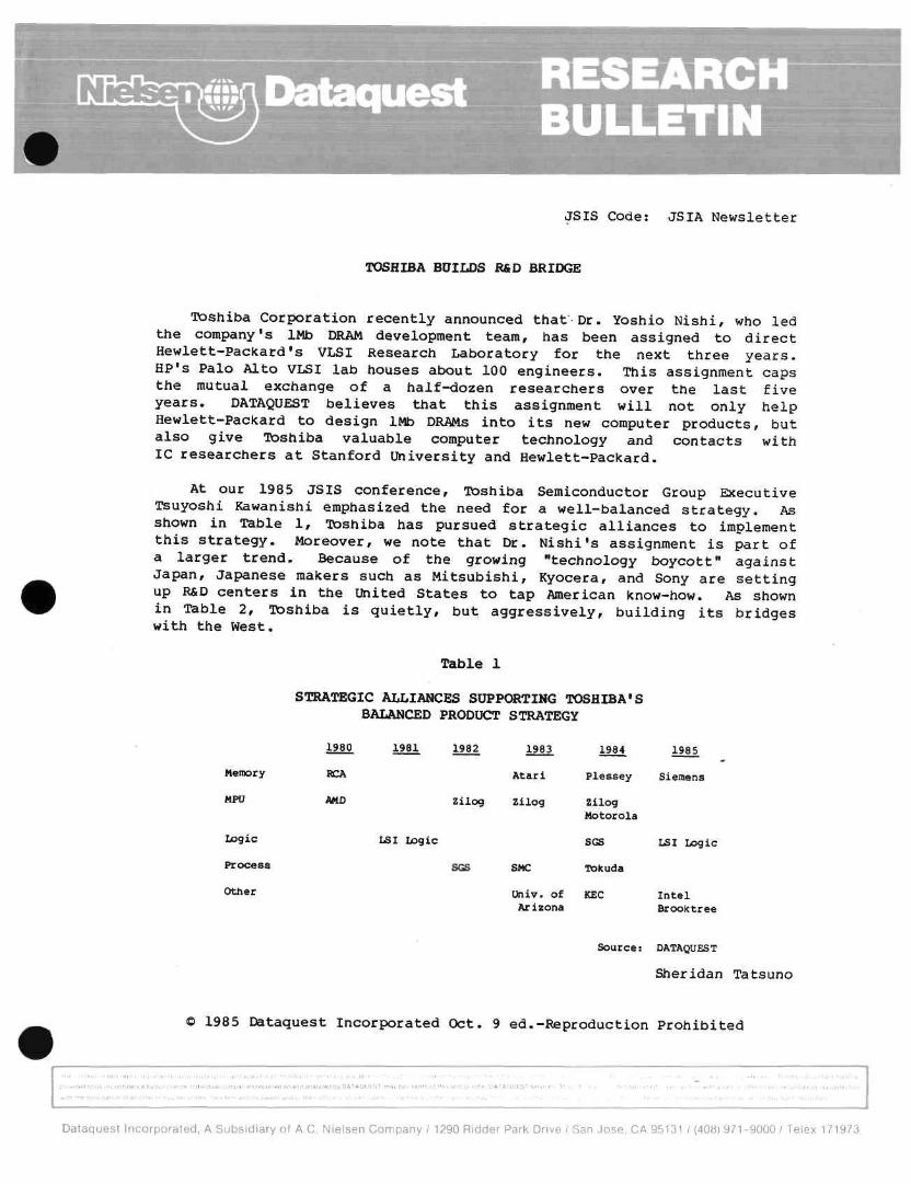
Dataquest RESEARCH BULLETIN
JSIS Code: JSIA Newsletter
TOSHIBA BUILDS R&D BRIDGE
Toshiba Corporation recently announced that Dr. Yoshio Nishi, who led the company's 1Mb DRAM development team, has been assigned to direct Hewlett-Packard's VLSI Research Laboratory for the next three years. HP's Palo Alto VLSI lab houses about 100 engineers. This assignment caps the mutual exchange of a half-dozen researchers over the last five years. DATAQUEST believes that this assignment will not only help Hewlett-Packard to design 1Mb DRAMs into its new computer products, but also give Toshiba valuable computer technology and contacts with IC researchers at Stanford university and Hewlett-Packard.
At our 1985 JSIS conference, Toshiba Semiconductor Group Executive Tsuyoshi Kawanishi emphasized the need for a well-balanced strategy. As shown in Table 1, Toshiba has pursued strategic alliances to implement this strategy. Moreover, we note that Dr. Nishi's assignment is part of a larger trend. Because of the growing "technology boycott" against Japan, Japanese makers such as Mitsubishi, Kyocera, and Sony are setting up R&D centers in the IMited States to tap American know-how. As shown in Table 2, Toshiba is quietly, but aggressively, building its bridges with the West.
Table 1
STRATEGIC ALLIANCES SUPPORTING TOSHIBA'S BALANCED PRODUCT STRATEGY
Heinory
MPU
Logic
Process
Other
1980
RCA
AMD
1981 1982
Zi log
LSI l o g i c
1983
Atari
Zilog
SMC
Univ . of Arizona
1984
P l e s s e y
Zi log Motorola
SGS
Tokuda
KEC
1985
Siemens
LSI Logic
I n t e l Brooktree
S o u r c e : DATAQUEST
Sheridan Tatsuno
1985 Dataquest Incorporated Oct. 9 ed.-Reproduction Prohibited
I^, 1, .Tn , i , I
pfovKlf i t 10 \)f, :'i ( on
* ' | t ; "l-r liwri: iM Mfi^
aence t j you ' c
1 • ' * n r T'
t
iie:ns
r l * '
,„.i.„. l-.Cl..ltlu,ll<C
mm. 1„„1
• r . .J4 | i« .k i^ V mn i . i . : . . ' .
^•pd'l|ps rcuorieo 0 " and jn,-i
"1 .nrt ilf. t.*l^rTT.f. i l . |. i r * -
. • . , 4 . 1 4.U I.I .
;ed by DATAQUE-ST
• " • ' • ' • • ' • • • • • •••-
IPS, t,C iienT, c Ih,sand or Hhp DATAOIJESI w , „ . , . , I . ., 1 •
''- -o - . -
. . .„
. . . , ^ . ^ .til mi]Ti'.Ma.*tr* Mi^Hll ^t^
I.I Lit'wi •i.it t - j , s ^ i- Bi
11 . - . l i l . . i l LL.'LJiii -^J!<i.4
I.COUt^iniiil .1 hi}ttplhh.ti»l
t ,Lj (^ ^Hi'iilliir.
Dataquest Incorporated, A Subsidiary of A C. Nielsen Company / 1290 Ridder Park Drive / San Jose, CA 95131 / (408) 971-9000 / Telex 171973
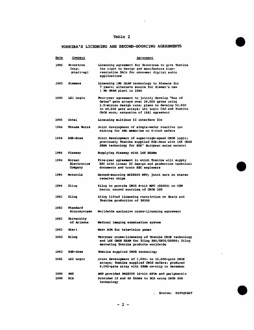
Table 2
TOSHIBA'S LICENSING AND SECOND-SOURCING AGREEMENTS
Date
1985
1985
1984
1984
1984
Company
Broolctree Corp . ( s tar t -up)
Siemens
1985 LSI Logic
1985 Intel
1984 Tolcuda WOrKs
1984 SGS-Ates
P l e s s e y
Korean Electronics Company
Motorola
1984 Zilog
1983 Zilog
1983
1983
1983
1982
Standard Microsystems
U i i v e r s i t y o f Arizona
Atari
Z i log
1982 SQ5-Ates
1981 LSI Logic
1980 AMD
1980 RCA
Agreement
Licensing agreement for Brooktree to give Tbshiba the right to design and manufacture high-resolution DACs for consumer digital audio applications
Licensing 1Mb DRAM technology to Siemens for 7 years; alternate source for Siemen's new 1 Mb DRAM plant in 1986
FDur-year agreement to jointly develop 'Sea of Gates* gate arrays over 20,000 gates using l.S-micron design rule; plans to develop 50,000 to 60,000 gate arrays; LSI Logic CAO and Toshiba CMOS worIc; extension of 1981 agreement
Licensing multibus II interface ICs
Joint development of single-wafer reactive ion etching for 4Mb memories on 6-inch wafers
Joint development of super-high-speed CMOS logic; previously Toshiba supplied SGS-Ates with leK 0408 SRAM technology for SGS' European sales networic
Supplying Plessey with 16K SRAMs
Five-year agreement in which Toshiba will supply K£C with linear IC design and production technical documents and train KEC engineers
Second-sourcing HC68000 MPU; joint worIc on stereo receiver chips
Zilog to provide CMOS 8-bit MPU (Z8000) on OEM basis; second sourcing of CMOS Z80
Zilog lifted licensing restriction on Sharp and Toshiba production of Z8000
worldwide exclusive cross-licensing agreement
Medical imaging examination system
Hasic ROM for television games
l>9n-year cross-licensing of Toshiba CMOS technology and 16K CMOS SRAM for Zilog Z80/Z800/Z8000; Zilog marlceting Toshiba products worldwide
Toshiba supplied CMOS technology
Joint development of 1,000- to 10,000-gate CMOS arrays; Ibshiba supplied anOS wafers; produced 6,000-gate array with SRAM on-chip in December
AMD provided AMZ8000 16-bit MPUs and peripherals Provided IK and 4K DRAMS to RCA using CMOS SOS technology
. Source: DATAQUEST
- 2 -
Dataquest RESEftRCH BULLETIN
JSIS Code: JSIA Newsletters
JAPANESE ELECTRONIC EQUIPMENT PRODUCTION TO REACH ¥18 TRILLION IN 1990
A recent report from the Japanese Electronics Industry Development Association (JEIDA) predicts Japanese electronic equipment production of almost YlB trillion (US$75 billion, at ¥240 per U.S. dollar).
The Japanese electronic equipment industry will achieve an overall compound annual growth rate (CAGR) of 9.2 percent from 1984 through 1990. The fastest growing product areas will be computers, electronic measuring instruments, and telecoiranunications equipment. Table 1 gives 1983 and 1984 historical production, plus JEIDA's forecast for 1985 and 1990.
JEIDA also predicts that total production of new media, home automation, office automation, and factory automation will be ¥7.0 trillion (US$29.2 billion) in 1990, more than doubling to ¥15.0 trillion (US$62.5 billion) by 1995. In 1995, new media and home automation are each expected to account for ¥1.2 trillion (US$5.0 billion), office automation for ¥9.6 trillion (US$40.0 billion), and factory automation for ¥3.0 trillion (US$12.5 billion).
DATAQUEST believes that Japanese telecommunications equipment production will experience faster growth than JEIDA forecasts, largely due to increased competition and easier access to the market brought about by the privatization of Nippon Telegraph and Telephone Public Corporation and the huge growth necessary to support totally integrated office automation (i.e., a network that can connect all kinds of computers among various companies and industries), which will exist in 1990.
Nagayoshi Nakano Patricia S. Cox
© 198 5 Dataquest Incorporated Oct. 8 ed.-Reproduction Prohibited
SJp:i-.Tftf l o I T * ^ t ^ — ' ^ * i M » liT * J f M * * * ^ Individual conipam .ily/P:; Ijy DATAOIJFST rr.sv li •f OATAQUF.ST • icrvKfs Th
Dataquest Incorporated, A Subsidiary of A.C. Nielsen Connpany / 1290 Ridder Park Drive / San Jose, CA 95131 / (408) 971-9000 / Telex 171973
Table 1
ESTIMATED JAPANESE ELECTRONIC EQUIPMENT PRODUCTION (Billions of Yen)
:al Electronic figuipment
Consumer TV VTR Other
Industrial
Telecommunications Equipment
Wired Equipment Broadcasting/Uireless Equipment
Computer
Electronic Measuring Instruments
Other Electronic Instruments and Medical Electronics
Business Machines
Hist 1983
V8,371.1
y3,742.6 706.1
1,516.4 l,S2a.l
ir4,628.5
1,475.9 938.8
537.1
1,955.3
462.2
434.2
300.9
orv 1984
(10,626.5
K 4,592.2 776.5
2,090.1 1,725.6
1 6,034.3
1,756.3 1,157.4
598.9
2,810.7
550.0
553.0
364.3
Forecast
1985
irl2,248.0
y 4,930.0 820.0
2,220.0 1,890.0
V 7,318.0
1,988.8 1,317.6
671.2
3,786.4
626.0
521.8
395.0
1990
¥17,990.5
y 5,430.0 850.0
2,350.0 2,230.0
112,560.5
3,016.4 1,999.5
1,016.9
7,036.6
1,147.0
798.0
562.5
Percent 1983-1984
26.9«
22.7% 10.0% 37.8% 13.5%
30.4%
19.0% 23.3%
11.5%
43.7%
19.0%
27.4%
21.1%
Growth
1984-1985
15.3%
7 . 4 %
5 . 6 %
6.2% 9.5%
21.3%
1 3 . 2 %
13.8%
12.1%
34.7%
13.8%
(5.6%)
8.4%
CAGR 1984-1990
9 . 2 %
2 . 8 %
1.5% 2 . 0 %
4.4%
13.0%
9 . 4 %
9.5%
9.2%
16.5%
13.0%
6 . 3 %
7.5%
Source! Japanese Electronics Industry Development Association Electronics Industry Association o£ Japan Ministry of International Trade and Industry
- 2 -
JSIS Code: JSIA Newsletters
NINTH ANNUAL SIA FORECAST DINNER; FORECASTING THE RECOVERY
SUMMARY
The Semiconductor Industry Association's ninth annual forecast dinner was held amid a mood of optimism combined with deep concern for the future viability of the U.S. semiconductor industry.
The evening began with a roast of retiring SIA president Tom Hinkelman and was emceed by Charlie Sporck, president of National Semiconductor Corporation. The featured speakers were Dr. Gil Amelio, president of Rockwell International's semiconductor products division, and Dr. Bob Noyce, vice chairman of Intel Corporation.
Mr. Sporck compared the U.S. semiconductor industry to a football player who is bleeding from an injury in a game where the competition is not penalized for breaking the rules. Although the U.S. industry has managed to survive under these conditions, the bleeding has not stopped. He called for forced change through "forms of leverage that some may call protectionist."
FORECAST
Dr. Amelio presented the consensus forecast for 1985 through 1986, which was prepared by the World Semiconductor Trade Statistics (WSTS) forecast committee, comprising representatives from 30 semiconductor manufacturers worldwide.
The WSTS forecast calls for a worldwide consumption decline of 17 percent in 1985, followed by three years of growth: 18 percent in 1986, 23 percent in 1987, and 23 percent in 1988. Over the long term, Japan will be the fastest-growing market, gaining several points in world market share in 1985 and maintaining them through 1988. Dr. Amelio pointed out that NMOS and PMOS memory are still showing no sign of recovery, while analog ICs are doing well, particularly in Japan, where the consumer electronics market is still fairly strong. Bipolar digital ICs are also doing well, having maintained a book-to-bill ratio of l.O since May.
1985 Dataquest Incorporated Sept. 30 ed.-Reproduction Prohibited
• „HI •yitCI^i I f f I^H". '
. Tr|n |ii|r.(4i^[5 i H f j j H
Dataquest Incorporated, A Subsidiary of A.C Nielsen Company / 1290 Bidder Park Drive / San Jose, CA 95131 / (408) 971-9000 / Telex 171973
Dr. Amelio pointed to several causes of 1985's disastrous market decline:
• A slowdown in the OEM market, particularly computers, which account for 40 percent of the U.S. semiconductor market
• A huge semiconductor inventory at OEMs (estimated to have been between $2 billion and $2.5 billion)
He believes that end users (i.e., consumers and businesses) have slowed consumption because they want more innovative products. OEMs will continue to slim down their semiconductor inventories as part of better asset management, but eventually demand will firm, as will prices. Finally, new, innovative products will spur end-user demand.
U.S.-JAPAN TRADE
Dr. Noyce's topic was U.S.-Japan trade friction. While admitting that many unfair trade practices do exist on the part of the Japanese, he believes that unfair practices are not the sole cause of the U.S. industry's current dilemma. Prior to 1980, the United States enjoyed years of trade surplus. Since 1980, however, the U.S. trade deficit has escalated dramatically. U.S. manufacturers are no longer competitive in the world market, Americans are substituting foreign sources of goods and services for domestic sources, and thousands of formerly U.S. manufacturing jobs are being moved offshore.
Dr. Noyce stated that the high value of the U.S. dollar bears a direct relationship to the current U.S. savings and trade deficits. The implication of this is that if the U.S. savings rate increases to the point of becoming a savings surplus, the U.S. dollar will fall in value and the trade deficit will become a trade surplus. Approximately 65 percent of U.S. corporate profits go into savings, while only 4.5 percent of personal income is saved. If President Reagan's tax proposal is passed, shifting more of the tax burden onto corporations and off of individuals, the resulting decrease in corporate profits would lower the corporate savings rate, decrease net savings in the country, and increase import penetration by $22 billion.
Dr. Noyce concluded that the solution to the problem is in the hands of the United States, which must produce a surplus of goods to send overseas, rather than bringing in goods from other countries. This can be done by increasing personal and government savings.
DATAQUEST ANALYSIS
A dichotomy of opinion on the trade issue was clearly in evidence at the dinner. Although most attendees agreed that free trade is best in the long run, many called for short-term protectionist measures. Even those against any form of protectionism would probably agree with Mr. Sporck's often-repeated rallying cry: "Protectionism beats extinction any day."
Patricia S. Cox
- 2 -
Dataquest JAPANESE RESEARCH NEWSLETTER
JSIS Code: JSIA Newsletters
JAPANESE SEMICONDUCTOR MARKET UPDATE
DATAQUEST has revised its forecast for Japanese semiconductor consumption in 1985 and 1986 based on recent events that suggest a more prolonged downturn than originally foreseen. Table 1 shows a comparison of this forecast and our previous forecast of June 18, 1985.
One of 1985's major growth markets for both Japanese-made semiconductors and Japanese-made end equipment, such as televisions and refrigerators, has been the People's Republic of China. However, recent government restrictions and a lack of foreign currency have caused cancellation of orders in the second half of 1985. Many Japanese electronics firms were hard hit by the change in policy, which has certainly contributed to the current depressed state of the Japanese market.
Because of Japan's preeminence in consumer electronics, the Japanese semiconductor market is not as dependent on the ups and downs of the computer marketplace as the U.S. semiconductor market is. Thus, while the U.S. marKet is expected to decline 31.4 percent in 1985 and to grow 9.8 percent in 1986, the Japanese market will decline only 5.2 percent in 1985 and grow 12.0 percent in 1986 (yen basis). This huge delta in growth rates between the two countries means that by the end of 1986, the Japanese marKet will have grown to 33.9 percent of the world market, up from 30.1 percent in 1984.
Figure 1 shows our estimates of the quarter-to-quarter percentage changes in Japanese semiconductor consumption from 1984 through 1986. Although the second quarter of this year was up a scant 0.6 percent, we believe that the third and fourth quarters will show negative growth. We do not expect shipments to picK up until the first quarter of 1986.
Table 2 shows our quarterly growth forecast for the Japanese market through 1986. MOS memory is clearly the hardest hit. product line this year, but it will show good recovery in 1986. Linear ICs and MOS logic devices will show positive growth this year, continuing into 1986.
Table 3 shows actual market values in yen for the same period as Table 1.
© 1985 Dataquest Incorporated Sept. 23 ed.-Reproduction Prohibited
The content of this report represents our interpretaion and analysis of information generally available to the public or released by responsible individuals in the subject companies, but is not guaranteed as to accuracy or completeness It does not contain material provided lo us in confidence by our clients Individual companies reported on and analyzed by DATAQUEST, may be clients of this and/or other DATAQUEST services This information is not furnished in connection with a sale or otter to sell securities or in connection with the solicitation of an oHer to buy securities This firm and its parent and/or their officers, stockholders, or mennbers of their families may, from time to time, have a long or short
Azabu Heights, Suite 711, 1-5-10 Roppongi, Minato-ku, Tokyo 106, Japan 1290 Ridder Park Drive / San Jose, CA 95131 / (408) 971-9000 / Telex 171973
t
Figures 2 and 3 are 12/12 rate-of-ctiange graphs. They are graphs of the percentage cnange of a moving 12-month total from the total for the same 12 months one year earlier. The resulting graphs show a smooth picture of the rate of change for a given product line.
Figure 2 shows historical and forecast rates of change for total semiconductor consumption. The point at which the line crosses the Y axis in December of each year is the yearly growth rate for that year. We estimate that this point will be -5.2 percent in December 1985. By December 1986, however, the rate of change is expected to reach 12.0 percent.
Figure 3 shows historical and forecast rates of change for MOS memory, MOS micro devices, and MOS logic. As shown, the growth rate for MOS memory is falling precipitously from 91.1 percent in December 1984 to an anticipated -25.5 percent in December 1985. We believe that the turn in rate of change will occur in the second quarter of 1986.
Patricia S. Cox Gene Norrett
- 2 -
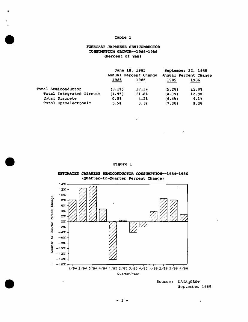
Table 1
FORECAST JAPANESE SEMICONDUCTOR CONSIMPTION GROWTH—1985-1986
(Percent of Yen)
TIDtal Semiconductor Total Integrated Circuit Total Discrete Total Optoelectronic
June 18, 1985 Annual Percent Change 1985 1986
September 23, 1985 Annual Percent Change 1985 1986
(3.2%) (4.9%) 0.5% 5.5%
17.3% 21.8% 4.2% 8.3%
(5.2%) (4.0%) (9.4%) (7.3%)
12.0% 12.9% 9.1% 9.3%
Figure 1
ESTIMATED JAPANESE SEMICONDUCTOR CONSUMPTION—1984-1986 (Quarter-to-Quarter Percent Ctiange)
14%
o
c a X
o ..J
c t> o <s a. o t: o -> O _o
L.
o t: o 3 (J
'
12%
10%
8%
6%
4%
2%
0%
- 2 %
- 4 %
- 6 %
- 8 %
-10% -12%
-14%
-16%
ii ^
/
1.^ •" I
JL
"TA
yr
/ . ^
1 1 1 1 1 1 1 1 r- 1 1 1 — 1/84 2/84 3/84 4/84 1/85 2/85 3/85 4/85 1/86 2/86 3/86 4/86
Quarter/Year
Source: DATAQUEST September 1985
- 3
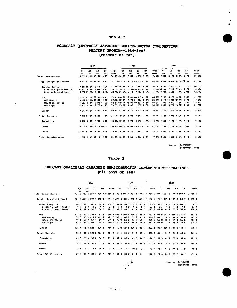
Table 2
FORECAST QUARTERLY JAPANESE SEMICONDUCTOR CONSUMPTION PERCENT GROWTH—1984-1986
(Percen t o f Yen)
Total Semi conductor
Total Integrated Circuit
Bipolar Dtgi tal
Bipolor Digital iJtemory Bipolar Digital Logic
MOS
MOS Memory
MOS Micro Device
MOS Log i c
Li neor
Totol Discrete
Tronsi stor
Diode
Other
Total Ootoelect ron Ic
01
— 8 V.
8 55!
7 er. 37 ax 4 75!
11 25!
9 45!
t 25!
27 45!
4 95!
7 6X
5 05!
10 15!
14 45!
11 6!!
02
12
13
18
8
19
11
14
8
8
14
11
8
15
11
8
65!
25!
25!
85!
55!
tx 85!
45!
2X
2%
65!
95!
85!
85!
45!
Q3
13
16
8
0
9
25
45 7
S
5
3
3
2
3
10
35!
35!
65!
05!
45!
35!
85!
9X 75!
45!
25!
9X
2X
25!
IS!
04
4
5
7
8
8
6
13
-1
-1
3
0
-a
2
8
75!
75!
3% \7. iX
45!
35!
2X 15!
95!
m
15!
85!
95!
55!
1984 01
51
57
41
59
39
74
93
42
79
40
36
36
36
40
33
75!-I4
55!-16
3S-18
05! 9
55!-21
4S-18
8R-32
65!-15
35! 13
65! -7
75! -8
15!-12
75! -6
55! 5
5K-16
25!
35!
45!
05!
65!
75!
25!
75!
95!
05!
ST.
T7.
5%
05!
95!
02
0
1
1
23
-2
9 -7
19 4
4
-4
-7
-2
5
0
6X
n
3X 35!-
15!
45!
75!-
9S
95!
15!
05!
25!
55!
75!
95!
03
-4
-4
-3 34
2
-9
21
-0 1
3
-3
-0
-5
-5
-5
95!
IX
65!
45!
45;
95!
5S
ex 15!
95!
ex
25!
9r.
45!
55!
04
-2
-2
-5
-5
-5
-2
-8
9
9
0
-1
-1
-1
1
-2
05!
25!
65!
\X 75!
77. 35!
85!
555
m
^x
35!
67.
m
95!
1985
-5
-4
-a 12
-11
-8
-25 -4
24
5
-9
-14
-7
13
-7
25!
05!
95!
15!
45!
05!
55!
55!
15!
S5!
45!
55!
85!
05!
35!
01
3
4
5
12
4
5
S
7
1
2
.i
3
i
0
-3
85!
45!
85!
55!
95!
45!
15!
ex SX
2X
25!
.65!
.55!
95!
37.
02
8
8
6
7
6
10
15
6
B
7
7
7
7
4
14
77.
ex
45!
95!
25!
},X ex ex 25!
55!
0X
15!
TX
77.
ex
03
8
8
1 1
7
11
9
18
7
3
5
5
4
8
3
9
Source:
15!
55!
05!
45!
45!
85!
15!
95!
9X
65!
9X
ex
ex
BX
45!
04
— .? • J 47.
2 IS!
1 77. 2.05!
2 85!
3 75!
1 95!
2 45!
1 95!
3 75!
3 15!
5 07.
1 77.
5 15!
DATAQUEST
September .
1986
12 05!
12 95!
10 95!
0 45!
12.4X
12 27.
7 25!
19 65!
12 55!
14 95!
9 15!
9 35!
9 97.
6 17.
9 i7.
1985
Table 3
FORECAST QUARTERLY JAPANESE SEMICONDUCTOR CONSUMPTION—1984-1986 (B i l l i on s o£ Yen)
1984 i9as
Total Semiconductor
Total Integrated Circuit
Bipolar Digi tol
Bipolar Digital Memory
Bipolar Digital Logic
MOS
MOS Memory
MOS Micro Device
MOS Logic
Linear
Total Discrete
Transi stor
Diode
Other
Total Optoelectronic
01 02 03 04 1984 Ql
434 5 489 2 554 4 580 7 2.058 9 498 2
321 2 363 5 422 9 446 9 1.554 5 378 3
48 3 57 1 62 0 66 9 234 3 54 6 5 7 6 2 6 2 6 7 24 8 7 3
42 6 50 9 55 7 60 3 209 5 47 3
171 5 190 6 238 8 254 2 855 I 206 7
74 8 85 9 125 2 141 9 427 8 96 2
49 1 53 2 57 4 56 7 216 4 47 8
47 7 51 6 56 1 55 5 210 9 62 7
101 4 115 8 122 I 125 8 465 1 117 0
89 6 109 0 103 2 103 2 396 0 94 1
49 5 53 9 56 9 56 9 215 4 48 9
31 6 36 6 37 4 37 1 142 7 34 7
8 5 9 5 9 8 10 0 37 8 10 5
23 7 25 7 28 3 30 7 198 4 25 8
02 03
501 0 481 0
384 7 368 8
55 3 53.3 9 0 5 9 46 3 47 4
207 6 188 9 88 8 69 7 53 0 52 7 65 8 66 5
121 8 126 6
99 3 87 6
45 4 45 3
33 8 318
n \ 19 5
26 0 24 6
rl
04
471 4
360 7
50 3 5 6 44 7
183 fl 63 9 53 1 66 B
126.6
86 6
44 7
31 3
10 6
24 1
1985
1.951 6
1 . 492 5
213 5 27 8 185.7
787 0
318 6
206 6
261 8
492 9
358 6
184 3
131 6
42 7
100 5
01
489 1
376 4
53 2
6 3
46 9
193 8 69 1 56 8 67 9
129 4
89 4
46 3
32 4
10 7
23 3
02
531 8
409 4
56 6 6 8 49 8
213 7 80 0 60 2 73 5
139 1
95 7
49 6
34 9
1 1 2
26 7
03
574 8
444 3
62 8 7 3
55 5
234 6 94 5 64 4 75 7
146 9
101 3
52 0
37 7
11 6
29 2
04
590 6
454 9
64 1
7 5
56 6
241 1
98 0
65 6 77 5
149 7
195 0
53 6
39 6
1 1 8
30.7
1986
2 .186 3
1 .685 9
236.7 27 9
208 8
883 2 341 6 247 0 294,6
565 1
391 4
291 5
144 6
45 3
109 9
Source: DATAOUEST September. 1985
- 4 -
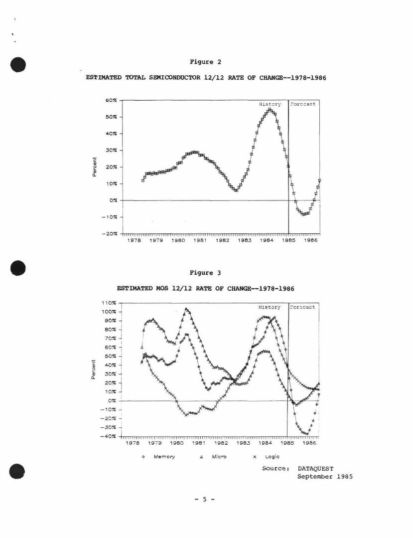
Figure 2
ESTIMATED TOTAL SEMICONDUCTOR 12/12 RATE OF CHANGE—1978-1986
6 0 %
5 0 % -
4 0 % -
3 0 % -
o 20%
a.
10% -
-10%
- 2 0 % l l l l l l 1 1 I T n I 1 I T I 1 I T I I I I I i l [ | l l l M ; [ I I I I I I I I I N I I T T T T I I 1 I I I I I I I I I I I I | l l [ I I I I I I I I I I l l I I I I l I I I ! n i l l l l l i l l M I
1 9 7 8 1 9 7 9 1 9 8 0 1981 1 9 8 2 1 9 8 3 198-4 1 9 8 5 1 9 8 6
Figure 3
ESTIMATED MOS 12/12 RATE OF CHANGE—1978-1986
110%
100%
90%
80% -
7 0 %
6 0 %
50% J
§ 4.0% o © 3 0 %
Q.
2 0 %
10%
0%
- 1 0 % -I
- 2 0 % -
- 3 0 % -
-4-0%
History rorocast
i i i i i i ' i i ! i r r n i i i r i i i ! i i i i i i M i r u n T T T i i i r i i i i i i i i i r : i i i i i i i i i i i i i i i i i i u i r u i . i i i i i l i ! l i | i i i | i ] i i i [ i ! ! [ l 1 9 7 8 1 9 7 9 1 9 8 0 1981 1 9 8 2 1 9 8 3 1 9 8 4 1 9 8 5 1 9 8 6
<• Memory A Micro X Logic
Source: DATAQUEST September 1985
- 5 -
Dataquest RESEARCtt BULLETIN
JSIS Code: EIEJ Newsletters
JAPAN PLANS NEW MARKET-OPENING MEASURES
On September 4, Motoo Shiina, Vice Chairman of the Policy Research Commission for Japan's Liberal Democratic Party (LDP), met with members of Stanford University's U.S.-Japan Forum to discuss trade friction issues. Mr. Shiina is a high-ranking LDP official responsible for drafting trade policies for Prime Minister Yasuhiro Nakasone. He is currently touring the United States to gather information and evaluate prevailing attitudes toward protectionism. Mr. Shiina made the following points during the discussion:
• Japanese export restraint may be necessary to defuse explosive trade friction, but it is only a short-term solution. Japanese market opening is the only long-term solution.
• MITI held a conference in June with 60 Japanese companies to request a ' $5 billion increase in purchases from the United States. These companies are already planning to purchase $2 billion in fiscal 1985, so an "affirmative action program" would only net about $3 billion. MITI is planning to call in another 73 companies to increase total purchases from the United States to 310 billion.
• Americans have requested that Japan implement policies to expand domestic demand, but Japan has limited policy options.
Lowering interest rates would weaken the yen further and increase Japanese exports to the United States, while raising interest rates would shut off domestic growth and reduce U.S. imports.
Increased public spending runs counter to the government's efforts to reduce its large budget deficits.
© 1985 Dataquest Incorporated Sept. 10 ed.-Reproduction Prohibited
:i Ci i^ tu i I imj IH
provided 10 us m i y DATAQUEST ma^ Jlhfir DATAQUEST 5
ng Of shori posi
Dataquest Incorporated, A Subsidiary of A C. Nielsen Company / 1290 Ridder Park Drive / San Jose, CA 95131 / (408) 971-9000 / Telex 171973
- Private investment in the public sector is being pursued, but it is difficult to implement in practice.
- Re-regulation of Japanese capital outflows would bolster the yen and free up funds for domestic spending. A 2 percent to 3 percent tax on interest income earned abroad might stem the current outflow.
Mr. Shiina said that Japanese officials are extremely worried about a protectionist backlash in the tJnited States this year, which would seriously weaken the Japanese economy. Thus, MITI is asking Japanese companies to help defuse the trade friction by buying more abroad. Even the Ministry of Posts and Telecommunications, which has been very protectionist to date, is beginning to feel the heat.
DATAQUEST believes that Prime Minister Nakasone will make another market-opening announcement this fall based on Mr. Shiina's policy recommendations. This announcement will probably elaborate on nis "affirmative action program" and possibly list the procurement plans announced by major Japanese companies. We note that Hitachi has already announced that it will spend $120 million by December 1986, while NEC will increase its purchases from $160 million to $200 million by 1987. Other major companies are expected to make their announcements this fall.
Sheridan Tatsuno
- 2 -
Dataquest RESEARCH BULLETIN
JSIS Code: JSIA Newsletters
TURNING THE TIDE: U.S. SailCONDUCTOR ACTIVITIES IN ASIA
The media has bombarded us in recent months with news about the demise of the U.S. semiconductor industry in the face of the Japanese and Korean challenges. How valid is this view? Are American makers destined to gradually decline? DATAQUEST believes that much of this reporting is sensationalism based on old |news—the excellent sales achieved by Japanese companies in 1984. However, with the collapse of the computer market, we note that Japanese semiconductor makers are losing share in the Iftiited States (see our trade update newsletter of July 10). Sales of MOS memory products, which accounted for 62 percent of total Japanese semiconductor exports to the United States in 1984, dropped 22 percent in the first half of 1985.
Moreover, we see signs of a serious effort by American makers to increase their presence in the Japanese market, as shown in Table 1. We believe that the following recent activities are significant:
• IBM's staffing up of its Tokyo office, its entry into the value-added network (VAN) market with Mitsubishi, and its patent licensing agreement with MITI
• Nihon LSI Logic's tie-up with Kawasaki Steel to enter the gate array and standard cell market
• New Japanese plants announced by Analog Devices, Fairchild, Monsanto, Motorola, and National Semiconductor
• Opening of new design centers in Tokyo by AMI, GE Semiconductor, ITT Semiconductor, National Semiconductor, Nissec Fairchild, and Syntek
• New investments in Taiwan by Mosel, Motorola, Syntek, Unicorn Microelectronics, and Vitelic
© 1985 Dataquest Incorporated Sept. 5 ed.-Reproduction Prohibited
(.. prOV
"""
...... , <ledioi ,s
Ihesol.r.
1 ih - ift^r
mronl iOc
l a i i o n o l a
1 lF<'l.1i.H.h. n *
i f . ebyou-c i .en is
l o t l e M o buy sec
i.^lLP.II.ir.1.1- .tMrJ ril..|
inOiviOual companies
' i f e s This (I'm anil .1
Cpo'IPdf
Daren! a
nana ana l ,
• " " " " " " "
. . . .*. . ..JM.„.„ . !ea by DATAQUEST
t i l l e's sIorhhfjKier!^
-ndvrR
n- m..,
• l e n T s f !
nn.>-sol i
h,. ,<„,!(! '
' • " ' " ' • " "
i..|,p„J,.ri<>- ' <<<
iitier DATAQUEST seiv
"••" ' ' ' " " • ' l-ne 10 l,rr,f
^,^ 1
ces T>ir
• 1 Uii. MIi l^dl 1+ i i iJ I^M4<.|I^i'*l1tI141lrllH-Jrnr*ikx.i ..bijiHi^Jc ie± i
11WI ' ' ; * ' ! n * ' * ^CI1'H'"• ^" I ' l l 1^ C^ -TW^ 1: in « I P K » u i r u ' p ^ l * ! T|i M
' i i i | I'j i i - i^ ' i r?in " Fi <nf «pirLiiilIF>iiin'i|iH4iiti]l*iii^ in * t t n ^mriLr
II biL z!:* rK>i c 1 i i *> " mi i l4 t4»
V i f u ^ n ' i t nr 11 GiliTn'KiTrnr"
t SwGti I tC t iF i ^m
Dataquest Incorporated, A Subsidiary of A.C Nielsen Company / 1290 Bidder Park Drive / San Jose, CA 95131 / (408) 971-9000 / Telex 171973
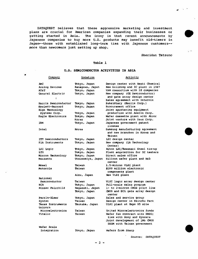
DATAQUEST believes that these aggressive marketing and investment plans are crucial for American companies expanding their businesses or getting started in Asia. The irony is that recent announcements by Japanese companies to buy more U.S. products may benefit old-timers in Japan—those with established long-term ties with Japanese customers— jnore than newcomers just setting up shop.
Sheridan Tatsuno
Table 1
U . S . SEMICONDUCTOR ACTIVITIES IN ASIA
Company Loca t ion A c t i v i t y
AMI Analog Devices AT&T General Electric
I
Harris Semiconductor Hewlett-Packard High Technology Systems Corp. Hugle Electronics
IBM
Intel
Tokyo, Japan Kanagawa, Japan Tokyo, Japan Tokyo, Japan
Tokyo, Japan Tokyo, Japan
Tokyo, Japan Tokyo, Japan Korea Tokyo, Japan
Korea
ITT Semiconductors KLA Instruments
LSI Logic LTX Micron Technology Monsanto
Mosel Motorola
National Semiconductor NCR Nissec Fairchild
Perkin-Elmer Syntek Texas Instruments Unicorn Microelectronics Vitelic
Tokyo, Japan Tokyo, Japan
Tokyo, Japan Tokyo, Japan Tokyo, Japan Utsunomiya, Japan
Taiwan Taiwan
Aizu, Japan
Taiwan Tokyo, Japan Nagasaki, Japan Tokyo, Japan
Tokyo, Japan Taiwan Tsukuba, Japan
Taiwan Taiwan
Wafer Scale Integration Tokyo, Japan
Etesign center with Asahi Chemical New building and IC plant in 1987 VAN consortium with 18 companies New company (GE Semiconductor) and gate array design center Sales agreement with Internix Subsidiary (Harris Corp.) Procurement office Joint sputtering equipment production with Anelva Corp. Wafer cassette plant with Atcor Joint venture with Zeus Corp. Japanese government patent license
Samsung manufacturing agreement and new branches in Korea and Taiwan LSI design center New company (LA Technology Center) Nihon LSI/Kawasaki Steel tie-up Plant acquisition for IC testers Direct sales office Silicon wafer plant and R&D center 1.5-micron VLSI plant $100 million electronic components plant New VLSI plant
VLSI logic array design center Full-scale sales program 1- to 2-micron CMOS pilot line CMOS and ECL gate array design center Sales and service group Design center in Hsinchu Park ULSI plant at Expo 85 site
United Microelectronics funds Wafer fab contract with ERSO; ties with Sony and Kyocera
Joint development of 1Mb CMOS DRAM with Taiwan government
Wafers from Sharp
Source: DATAQUEST
- 2 -
Dataquest ^JAPANESE — RESEARCH NEWSLETTER
JSIA Code: Newsletters
JAPANESE SEMICONDUCTOR TECHNOLOGY TRENDS Second Quarter 1985
SUMMARY
Despite the severe industry downturn, the outpouring of new Japanese technologies and products is accelerating. During the second quarter, DATAQUEST observed a rapid shift from commodity items to application-specific memories (ASMs), original MPUs/MCUs, gate arrays, standard cells, and optically based sensors and ICs. New applications are also being pursued, such as IC memory cards, 8mm video cameras, high-definition and sound multiplex televisions, facsimiles, medical diagnostic tools, optical communications, voice synthesis/recognition, graphics and television displays, and laser printers. We also note that MITI's 10-year joint R&D projects are half way through completion and spinning off new technologies.
DATAQUEST believes that the following developments in semiconductor technology are significant.
Japanese
Basic Research
• Opening of new corporate R&D centers (NEC, Tokyo Sanyo, TDK)
• MITI's planned new synthetic diamond substrate joint R&D project
• Expansion of the installed base of supercomputers
• Progress in 3-dimensional ICs and superlattices at MITI's New Function Elements Project (1981-1990)
New Products and Device Technologies
• Sampling of 1Mb DRAMs (Fujitsu, Hitachi, Oki, and Toshiba)
• Introduction of high-speed bipolar CMOS (Hi-Bi-CMOS) 64K SRAMs (Hitachi) and gate arrays (Toshiba)
for
© 1985 Dataquest Incorporated Aug. 16 ed.-Reprodiaction Prohibited
The content of this, report represents our interpretaion and analysis of information generalIy available to the public or released by responsible individuals in the subject companies, but is not guaranteed as to accuracy or completeness lt does not contain material provided to us in confidence by our clients Individual companies reponed on and analyzed by DATAQUEST, may be clients of this and/or other DATAQUEST services This information is not furnished in connection with a sale or offer to sell secunties or in connection with the solicitation o( an ofler to buy securities This firm and its parent and/or their officers, stockholders, or members of their families may, from time to time, have a long or short position in tne securmes mennonea ana may seii ur uuy au^ii aubunliea
Azabu Heights, Suite 711, 1-5-10 Roppongi, Minato-ku, Tokyo 106, Japan 1290 Bidder Park Drive / San Jose. CA 95131 / (408) 971-9000 / Telex 171973
Rapid growth in IC cards with MPUs, EPROMs, and EEPROMs for bankingf credit, and medical identificationr and for data processing (Kyodo Printingf Mitsubishi, and Dai Nippon)
Development of a three-level polysilicon structure for CMOS EEPROMs (Toshiba)
Proliferation of original 8-bit and 16-bit CMOS MPUs and intense research on application-specific .16-bit MCU "superchips" (Hitachi, Japan Victor, Mitsubishi, and NEC)
Introduction of a 3-D CMOS 16-bit MPU (Matsushita)
Development work on 32-bit MPUs (Hitachi, NEC, and Oki)
Marketing of a V20/V30 MPU development support system (Sony/ Tektronix)
Development of digital signal processors (DSP) for television and graphics displays and speech recognition (Fujitsu, Hitachi, Mitsubishi, and NEC)
Introduction of CMOS standard cell libraries (Asahi Microsystems, Fujitsu, Japan Victor, Matsushita, Mitsubishi, NEC, Ricoh, Sharp, Toshiba, and Yamaha)
Use of semiconductor lasers in car systems (Nissan); optical disks, television animation, audio, and video disks (NEC); copiers, printers, POS, and OA equipment (Sharp)
Use of CCD image sensors for video cameras, sound multiplex and high-definition televisions, facsimiles, copiers, and computer input (Fuji Photo Film, Matsushita, Mitsubishi, NEC, Olympus, TI Japan, and Toshiba)
Development of GaAs logic ICs for high-speed multiplexed communication signals (Matsustiita)
Use of biosensors in medical diagnostic tools and artificial human organs (Matsushita); and bioelectronic research (NEC/MITI)
Equipment, Materials, and Packaging
• An excimer laser photolithographic unit for 16Mb DRAMs and electron-beam lithography, and fog exposure technology for 64Mb-level DRAMs (Toshiba)
• New equipment for photomask correction (NEC); wafer particle detection (Hitachi); and fully automatic defect detection (NJS)
• Ultra high-speed electron beam testing (Hitachi)
#
- 2 -
• Zig-zag in-line packaging (ZIP) for 256K DRAMs (Fujitsu and Mitsubishi)
* Replacement of gold wire bonding with copper wire bonding (Mitsubishi)
CORPORATE R&D LABS
NEC has establish a ¥10 billion ($40 million) R&D center within its Sagamihara Works near Tokyo to develop silicon wafers for next-generation ICs, sucii as 4Mb DRAMs and 32-bit MPUs. The center comprises 3,000 square meters of space and has highly sophisticated equipment.
Tokyo Sanyo Electric has announced plans to build a new R&D center and laboratory by next spring either in its main plant or in the VLSI plant in Niigata Sanyo Electric. The center will focus on 4Mb and higher VLSIs.
TDK Corporation, the world's largest maker of ferrites and magnetic tapes with V178.8 billion (3715 million) in sales in 1984, announced that it will enter, ttie semiconductor market. The company plans to build a Semiconductor Technology Technical Center in Saku, Nagano Prefecture, by the end of this year. The two-storied ¥4.5 billion plant ($18 million) will produce thin-film magnetic heads for its hard disk drives. Its 200 to 300 researchers will focus on GaAs sensors, high-power transistors, and thermal printer drive ICs.
The Japanese government plays a major role in promoting joint research in next-generation semiconductors. During the second quarter, the Ministry of International Trade and Industry (MITI) and Nippon Telegraph and Telephone (NTT) made the following announcements that we believe will greatly affect the semiconductor industry:
GOVERNMENT R&O PROJECTS
Nippon Telegraph and Telephone's (NTT) Information network System (INS)
NTT announced on May 21 that it will invest ¥1.66 trillion ($6.64 billion) in plant and equipment in fiscal 1985, including ¥480 billion ($1.92 billion), in its nationwide Information Network System. DATAQUEST believes that in 1985, the semiconductor content of the telecommunications equipment procured by NTT will be approximately 12 percent, or $800 million. Of this amount, INS procurement will
- 3 -
account for $230 million. In fiscal 1984, NTT invested about ¥380 billion ($1.52 billion) in INS, of which we believe semiconductors accounted for about 11.5 percent, or $175 million. NTT is also increasing its R&D budget. In fiscal 1985, NTT plans to spend ¥170 billion ($680 million) for basic research, which is about six times the amount spent by the Ministry of International Trade and Industry (MITI) .,
MITI New Diamond Porum
MITI recently held an inaugural meeting of the New Diamond Forum to discuss the possibility of using synthetic diamonds as substrates for future semiconductors. About 200 companies from the electronic, automotive, steel, and other industries are being sought to form a joint goverrunent-industry R&D project and to secure budget support starting in fiscal 1987. MITI is attempting to catch up with the United States, which is currently using synthetic diamonds in space electronic equipment. Materials with better heat resistance and thermal conductance are required for faster data processing speeds and extreme conditions, such as space, aviation, nuclear power plants, and automobile engines.
MITI Supercomputer Project (1981-1990)
Fujitsu has added two supercomputers to its VP series. The high-end machine (VP400) executes 1.14 GFLOPS (billion floating-point operations per second) and has a maximum memory of 256 megabytes, 128 kilobytes of vector register, and 2,048-byte mask register. The entry-level machine (VP50) handles 140 MFLOPS (million floating-point operations per second) and offers a 128-megabyte maximum memory, a 32-kilobyte vector register, and a 512-byte mask register. Both machines have 64 kilobytes of buffer storage, a maximum of 32 channels, and a maximum transfer speed of 96 megabytes per second. They are compatible with IBM's M series mainframes and can perform vector processing. The VP400 will be delivered starting in December and leased at ¥79 million ($322,450) per month. The VP50 will be shipped in September and leased at ¥46,000 ($184,000) per month. DATAQUEST observes that the VP400 is competitive with NEC's SX2 (1.3 GFLOPS), the Cray 2 (2.0 GFLOPS), and Hitachi's S810 (630 MFLOPS).
Supercomputer makers are gradually increasing their installed base in Japan. DATAQUEST notes that several companies and research centers have purchased or are planning to purchase a supercomputer, as shown in Table 1.
- 4 -
Table 1
R£C£NT SUPERCOMPUTER PURCHASES IN JAPAN
Computer Maker
Cray Research
Fujitsu
Model
Cray 1
Cray X-MP
VPIOO
Hitachi S810 SX-2
Purchaser
Mitsubishi Central Research Lab Toshiba Research Lab Nippon Telegraph and Telephone
Nissan Motor Company (36.5 million; planned)
Nagoya University Plasma Research Lab Kyoto University Data Processing Center Japan Nuclear Research Lab Power Generation & Nuclear Fuel Development Agency Toyota Motors (planned)
Tokyo University Data Processing Center Osaka University
Source: DATAQUEST
MITI New Semiconductor Function Elements Project (1981-1990)
On June 28, Shigeru Fukuda, a Fujitsu employee and current manager of MITI's superlattice research, gave a presentation at DATAQUEST on the status of the New Function Elements Project. DATAQUEST believes this is MITI's VLSI Project for the 1980s, which will introduce next-generation technologies, including 3-dimensional ICs, superlattice devices (silicon and GaAs), and hardened ICs. Due to national budget deficits, the project is only budgeted for ¥1.2 billion (34.5 million) in fiscal 1985, half the originally scheduled amount. Nevertheless, the member companies are increasing their R&D spending in these areas. We will issue a special newsletter examining the progress of this important project.
To date, the project has generated 373 papers and 282 patents (pending), as shown in Tables 2 and 3, respectively.
Almost two-thirds of the papers and pending patents in Tables 2 and 3 are for 3-dimensional ICs. When asked about this trend, the previous research manager, Mr. Kawashima, explained that MITI has decided to focus its efforts on 3-D ICs, where it believes Japan has a two-^ear lead over the West. In contrast, he noted that Japan is about six to seven years behind in hardened ICs, and is about equal in superlattices. In addition to developing new "bargaining chips" to trade with the West, DATAQUEST
- 5 -
believes that MITI has chosen the 3-D IC because of its immediate applications to 4Mb and 16Mb DRAM research. New 3-D technology will enable Japanese companies to develop faster memory and logic chips using the new configurations.
Table 2
MITI NEW FUNCTION ELEMENTS PROJECT (Technical Papers)
Fiscal Year
1981 1982 1983 1984
Superlattice Devices
1 11 31 33
3-Dimens iona1 ICs
6 53 86 85
Hardened ICs
0 18 30 19
Total
7 82 147 137
Total 176 230 67 373
Table 3
NQf SEMICONDUCTOR FONCTION ELEMENTS PROJECT (Patents Pending Iftider Contract)
Fiscal Year
1981 1982 1983 1984
Superlattice Devices
1 6 16 10
3-Dimensional ICs
6 64 75 74
Hardened ICs
1 10 12 7
Total
8 80 103 91
Total 33 219 30 282
Source: DATAQUEST
- 6 -
MITI's Institute of Indus'trial Technology
The Institute of Industrial Technology recently unveiled a prototype reading machine that automatically turns pages, reads books in Japanese, and vocalizes the words synthetically. The system consists of a robot manipulator page turner linked to an optical character reader. MITI plans to develop a commercially viable machine by 1988 for use by the blind and handicapped. The price will be about ¥30 million ($120,000). DATAQUEST believes that a limited market for optical sensors and voice synthesis chips will develop around this product.
NEW PRODUCTS AND TECHNOLOGY TRENDS
In past newsletters, DATAQUEST reported technology trends (advanced research and prototype development) and new products announcements in separate sections. Beginning with titiis newsletter, we will combine the two sections into a single New Products and Technology Trends section. To monitor Japanese trends, we'use the following rule of thumb: Japanese technical papers generally precede prototype devices by 12 to 18 months, product samples by 24 months, and mass production by 30 to 36 months, depending upon the market demand.
Memory
Although production of 256K DRAMs has just begun, Japanese makers have announced that they will begin sampling 1Mb DRAMs. By the end of 1985, DATAQUEST believes that Fujitsu, Hitachi, Oki, and Toshiba will begin sampling, while NEC will take a more prudent stance by not preceding these makers. Matsushita and Mitsubishi will start sample shipments in early 1986.
• Fujitsu—256K DRAMs in zig-zag in-line package (ZIP) and PLCC packages; access times of 100/120/150ns; sample prices of ¥3,700 ($14.80) for ZIP devices and ¥3,500 ($14) for PLCC devices
• Gold Star—Plans to sample 64K CMOS SRAMs starting in August
• Hitachi—A high-speed bipolar-CMOS (HiBiCMOS) 64K SRAM (HM6787) with ECL speeds and CMOS low-power consumption; 25ns access time; 220mW power consumption during operation and 16mA driving output power; TTL-compatible; 8.5x3.4mm; 22-pin CERDIP package 22-pin 300-mil ceramic DIP; sampling price of ¥15,000 ($60), or ¥8,000 ($32) for lots of 1,000; monthly production of 300,000 to 500,000 units
Six CMOS 25 6K SRAM models; general types and battery backup type; 85/100/120ns access times; 1.3-micron rule; 1.6 million transistors on a 4.98x9.4mm chip; shiEHAents in June; sample prices between ¥15,000 ($60) and ¥22,000 ($88); monthly production of 200,000 by late 1985
- 7 -
A CMOS' 256K EPROM with low program voltage of 12.5 volts (HN27C256); access times of 200/250/300ns; 200ns device sampling at ¥5^000 ($20) for orders of 10,000; developed using polysilicon EMOS technology
Two CMOS 256K SRAM versions, one with battery backup, and three access times (85/100/120ns); 28-pin plastic DIP packages
Sampling of 1Mb DRAMs; static column CMOS type; 4.66x10.1mm
A 64K SRAM in a 3G0-mil slim-line package (HM6264ASP); access times of 120/150ns; power dissipation of 15mW during operation and lOmW at standby; 8,192x8-bit parts sampling at ¥4,000 ($16)
A prototype 16Mb magnetic bubble memory developed using ion implant technology; conventional Permalloy transfer circuit and ion implanter circuit combined on ttie chip; commercialization planned for mid-1986, witti 64Mb model by 1989
• Matsushita—An 8-bit content-addressable memory (CAM) for use in non-Neumann logic computers; 30x36^nicron device with 3-layer blocks for checking data block by block; 236x32-bit memory structure; 99,000 transistor equivalent
Two NMOS 128K DRAMs using 2-micron silicon gate process; 128Kxl-bit structure; chip size of 3.8 x 5.16mm; 16-pin DIL package; access time of 120ns (MN41128-12) and 150ns (MN41128-15); priced at ¥550 (32.20); monthly production of 50,000 units to be increased to 500,000 units by late 1985; 2ig zag in-line package (ZIP) and PLCC
• Mitsubishi—256K DRAMs in two package types; three access speeds and page or nibble mode available for each type; device in PLCC package one-third tlie size of DIP-mounted devices (M5M4256J) ; device in zig-zag in-line package (ZIP) using through-hole mounting (M5M4256L); PLCC versions priced at ¥5000 ($20) for 120ns, ¥4500 ($18) for 150ns, and ¥4000 ($16) for 200ns; ZIP devices priced at ¥3800 ($15.20) for 120ns, ¥3400 (13.60) for 150ns, and ¥3000 ($12) for 200ns
A NMOS 256K EPROM using 2-micron rule N-channel silicon gate process; 200/250/300ns access times; sample shifsnents in June; initial monthly production of 50,000 units; priced at ¥4,000 ($16)
A line of 16K SRAMs (M5M21C67P); 16Kxl-bit and 4Kx4-bit types; 35/45/55ns access times; sample price of ¥2,000 ($8) for 35ns types
An NMOS silicon gate 1Mb ROM (M5M231000P) available in 250 and 300ns access times; 28-pin DIL plastic package; sample price of ¥6,000 ($24)
- 8 -
• NEC—A pseudostatic 256K RAM combining NMOS and CMOS DRAM functions {uPD42832C); available in 100/120/150ns; 32Kx8-bit structure pin-compatible with similarly structured CMOS SRAMs; 4.6 X 9.0mm; 28-pin DIP package; ¥6,000 ($24) sample price for 150ns type
• Ricoti—A 256K CMOS EPROM with 12.5V write voltage and 150ns access time; 2-layer silicon with 1.5-micron pattern, with a sense circuit to accept wide voltage fluctuation; sample prices Of ¥4,000 ($16)
«l Toshiba—8 percent to 9 percent yields with free 1Mb DRAMs being given to a limited number of users; sampling expected when yields exceed 10 percent
A 64K CMOS GEPROM with 50ns access time; 1 transistor, 3-level polysilicon structure; 2-inicron n-channel CMOS; 5.95x4.88mm chip; power consumption of 25mW during operation
Application-Specific Memory (ASM)
• Dai Nippon Printing—An optical memory card with 422 kilobytes of storage capacity (160 pages of A4 size text); production cost about $1.20; priced at $20 to 40; enhancement of storage capacity to 2 megabytes possible with fine pattern drawing technology; data read-out only using COD line sensors
• Fujitsu—A hybrid device combining a 2,375-gate array and 1,024-bit SRAM on a 6.7x7.1mm chip; 2.2ns delay time; four types (256x4/128x8/ 64x16/32x32)
• Kyodo Printing—16K, 64K, and 128K IC cards with EPROMs and EEPROMs in 16K and 64K capacities; two types of 8C card read-write machines for processing data
• Mitsubishi—Five types of IC memory smart cards; sample 1.8mm mask ROM card priced at ¥4,500 (518); EPROM card with 8-bit MPU at ¥10,000 (540); card witti 8-bit MPU and 64K SRAM for computer data files at ¥15,000 (560) ; an ISO-standard 0.75mm thick IC card with MPU and EPROM being developed for banking and credit uses
• NEC~A CMOS 2Mb mask ROM (uPD23C2000C) integrating 2.4 million elements and capable of storing 8,000 kanji characters; 6.63 X 8.42mm chip; 1.2-micron geometry; 250ns access time; power dissipation of 40 milliamperes during operation and 100 microamps at standby; 131,072 x 16-bit for word mode designation and 262,144 x 8-bit for byte mode; plastic or ceramic 40-pin 400 mil DIP; for use in portable Japanese language word processors, hand-held computers, and typewriters; priced at ¥8,000 ($32) each in lots of 1,000
- 9 -
Sharp—Four 1.2Mb CMOS kanji character generators (LH53012 series); suitable for CRT displays; I/O TTL-compatible; single +5V power supply; 3-state output; 40-pin plastic DIP; priced at ¥13,500 (354)
Suwa Seikosha—A CMOS tone-pulse telephone dialing circuit; 10-extensionf 18-digit repeat memory devices for telephone number storage and 24-digit redial memory capability; 20,000 devices'per month production
Microprocessors/Microcontrollers
• Fujitsu—Three NMOS and one CMOS one-chip MPUs with 256-word RAM capacity and power-on reset circuit; optional selection of 4-bit units; 4,096x8-bit ROM capacity
Sample shipments of 8-bit and 16-bit MPOs (80186/80188/ 80286) licensed from Intel
Two CMOS 4-bit MCUs added to a total of 14 series and 40 models; MB88201H witti 0.5 Kbyte ROM and 16x4-bit RAM and MB88202H with 1 Kbyte ROM and 32x4-bit RAM; sample shipments at ¥230 ($0.92) and ¥280 ($1.12), respectively; also a low-price, general-purpose MCU with built-in A/D converter (MB88211) priced at ¥360 ($1.44) for 1,000-unit orders; initial monthly production Of 200,000
• Hitachi—Two proprietary CMOS 8-bit MPUs with 4K EPROM and memory peripherals for the 6305 series; HD6505V mask ROM and HD6375V with 256K EPROM; 31 I/O ports, serial interface, and two timers; software-compatible and 192-byte RAM; minimum execution times of 0.5, 0.67, and Ins; 40-pin package
A CMOS 8-bit single-chip MPU with 4 Kbytes of mask ROM and EPROM (HD6305V) ; 54-pin flat package; 1.0/1.5/2.OMHz speed; wait mode lOmW; operating mode 35mW; sample price of ¥1,500 ($6); also an 8-bit MCU with an EPROM (HD63705V); sample price of ¥8,000 ($32)
Two original 8-bit CMOS single-chip MCUs using a 40-pin package; one device with mask ROM (HD6305V) and another with an EPROM; 40-pin package
Three CMOS 8-bit MCUs (Zero Turnaround Time); plastic package; shipments from May at ¥2,000-¥3,800 ($8-15.20)
A real-time operating system for measurement and control systems using 16-bit MCUs; parallel program development possible by mounting CP/M-68K as a second operating system; 27 to 28 modules
- 10 -
Matsushita—An original 3-dimensional CMOS 16-bit MPU (MN1617) developed using silicon-gate/ 2-micron gate patternsr and 2-layer, 3-D aluminum wiring patterns; 200ns execution time with 200mW power consumption at 20 MHz; SOmW at standby; 64-pin flat package; priced at ¥10,000 (340); sales since June
An original NMOS silicon-gate, 8-bit MPU (MN18900) using 2.5-micron rule; parallel processing with two 8-bit microprocessors and timing based on paired, 16-bit timer counters; 51 I/O parts, 4K ROM, and 256-byte RAM; expandable to 64K; 500ns execution time; 64-pin, shrink DIP package
A series of CMOS 4-bit MCUs (MN1700 series); 2-micron silicon gate process; multiplication direction function witti 1 microsecond direction cycle; MN1758 with 8K ROM and 512-word RAM sampling at ¥2,000 ($8); EP17516 piggyback type at ¥20,000 ($80) ; MN1799 evaluator witii 16K ROM and 512-word RAM at ¥6,000 ($30)
A CRT controller (MN8355) with a built-in erasable RAM; transfer speed of 30ns/dot in monochrome and SOOns/pixel (16-bit gradation) in color; shipments starting in September; sample price of ¥20,000 ($80)
Mitsubishi—An 8-bit CMOS MPU incorporating an A/D converter, timer/event counter, and universal asynchronous receiver/ transmitter (M50734-SP); for use in electronic typewriters, hand-held computers, copiers, and electronic musical instruments; priced at ¥1,450 ($5.80) ; monthly production of 100,000
A flexible disk drive single-chip MCU (M52810FP) designed for portable computers; fabricated using Bi-CMOS wafer processing; SOmW power dissipation; sample price of ¥2,000 ($8) ; monthly production of 200,000 units
Plans for sample shipment of 16-bit MCU prototypes within one year; 32-bit MPU also being developed
NEC—A CMOS 16-bit direct-memory access (DMA) controller (UPD71071C) ; transmits data at 5.3Mb/sec at 8 MHz without an MPU; four separate DMA channels consisting of 5,000 elements; 2-micron; 16Mb of address space; capable of interfacing with 8-or 16-bit MPUs; four independent built-in DMA channels; monthly production of 50,000 doubling by late 1985
Sampling of CMOS 8-bit V40 (uPD70208) and CMOS 16-bit V50 (UPD70216) MPUs starting this summer; 68-pin leadless chip carrier; 4-channel CMA controller; DRAM refresh controller; 8-level controller; 16-bit timer/counter; programmable wait function; serial interface; 64 Kbyte I/O space
- 11 -
A CMOS flexible disk format controller (MB89311), which is compatible with NEC's NMOS flexible disk controller (MB8877A); sample shipments in August; priced at v2,500 ($10)
Two 4-bit CMOS MPUs with peripherals having the performance of 8-bit MPUs; 0.95-microsecond command execution time for the central processor; first of NEC's uC0MOS-75X series, including the UPDD75106CW with a 6K mask ROM and the uPD75Pl08DW with an 8K EPROM
• Oki Electric—An advanced 8-bit MCU (80C51) with 4Kx8-bit ROM and 128x8-bit RAM; 12rMHz operating frequency; capable of executing the same instruction set used with Intel's HMOS 8051; 111 instructions, including hardware multiply and divide; 32 I/O lines organized into four 8-bit ports; priced at if3,500 (314) ; monthly production of 5OK to 10OK
Development of proprietary 32-bit MPU for introduction by late 1985; plans for captive use in minicomputers; second-sourcing agreements also being sought
• Sanyo—An NMOS 8-bit, single-chip MPU with built-in 8-bit bus interface for apparatus control (LM8854); 16K ROM; 2K RAM; 5V power supply; 64-pin shrink DIP; priced at ¥700 ($2.80)
• Sony—Three CMOS 4-bit MCU devices; a 64-pin, piggyback MCU (CXP5020) for debugging and evaluating; a general-purpose MCU (CXP5034) with 4K ROM and RAM structure; one MCU with an 8K external EPROM extension
Sony/Tektronix—NEC V20/V30 MPU development support system that can also handle Motorola 68010 and Intel 80186
Original 8-bit CMOS single-ctiip MCU planned for commercialization within one year; 4-bit MCU (SPC-5000 series) available since late 1984; second sourcing of NEC's 16-bit V20 and V30 MPUs
• Suwa Seikostia—4-bit and 8-bit CMOS, one-chip MCUs; 8-bit SMC8340F series with 4K ROM and 128 bytes of RAM; 4-bit SMC4040C MPUs with 512-byte ROM and 16x4-bit RAM
• Toshiba—A CMOS 4-bit MPU for handling truncated dialing and automatic redialing, with a dual-time, multifrequency tone dialer; 38.2x14.2mm; 2K ROM and 256x4-bit ROM configuration for repeat dialing; 31 I/O ports; 42-pin shrink package
A real-time clock LSI (TC8250P) for constant time control; display timer and refresh for repeated image display at 1mA power consumption; 16-pin DIP package; ¥500 sample price (32); also a CRT controller LSI (TC8505P) with display timing and memory refresh for repeated image display
- 12 -
Digital Signal Processors (DSP)
• Fujitsu—Two CMOS high-efficiency television display controllers capable of controlling the display of 180 characters and symbols on CRTs; sample prices of ¥1,000 ($4.00) for 1,000-unit orders of the MB88323 and ¥1,300 (35.20) for the MB88324; shipments from late 1985
• Hitachi—A bipolar CHOS digital signal processing RAM with a LED and 280-bit SRAM; 400-MHz bipolar transistor; 80mA, 9-segment LED; 12.7V power voltage; 1,500 gates; 5-micron silicon gate CMOS; S.OxS.Siran chip size
• Matsushita—Two speech signal processors connected to a minicomputer; LPC analysis and 2-channel filter analysis performed by DSP-1; input parameter compared to phoneme standard pattern by DSP-2; calculations executed in real time
A graphics display control processor (MN8350) for CRTs and LCD displays; CMOS silicon gate; 2.0^nicron process; shrink DIP and flat package; 10-MHz operating frequency; 300 mmW power consumption; sample price of ¥10,000 ($40); shipments from fall 1985
Two high-function DSP LSis with twice the processing capacity as conventional models; MN1909 priced at ¥100,000 ($50) ; MN1901 with 8K built-in ROM priced at ¥5,000 ($20)
• NEC—^A high-performance LSI (uPD7764) for DP matching processes; NMOS chip with 40,000 devices for speech recognition template matching; 40-pin standard package; capable of matching about 300 discrete words and recognizing 30 connected words by two-level DP matching
Application-Specific ICs (ASICs)
• Fujitsu—A hybrid device combining a 2,375-gate array and 1,024-bit SRAM on a 6.7 x 7.1mm chip; 2.2ns delay; four architectures (256x4/128x8/64x16/32x32) ; 13 package types up to 135-pin grid array; 2.3-micron rule for the SRAM portion
A standard cell library with 100 cells; CMOS parts with 2.1ns per gate delay time; orders accepted in Tokyo, Osaka, and Santa Clara; new design centers planned for Boston, Dallas, and Manchester, U.K.; recent standard cell entrants include Nippon Gakki (Yamaha), Asahi Microsystems, Otoshiba, Sharp, NEC, Japan Victor (JVC), and Mitsubishi
• Hitachi—Six CMOS gate array products with from 448 to 2,560 gates; (HG61H Series); 2ns delay time; capable of mounting SRAMs; can be designed with Daisy and Mentor CAD workstations; $2.00 to $9.40 for 40-pin package devices in lots of 10,000
- 13 -
• Matsushita—An original standard cell CAD system capable of developing full-custom LSIs; cell library of 200 cells, including various functional blocks of RAMs, ROMs, comparators, A/D and D/A converters
A new CAD program (SMILE) for automatic layout of 10,000-gate class LSIs within 6 minutes; layout time 1/5 to 1/20 of conventional methods due to new method of wiring and block arrangement; developed experimental DSP LSI for portable CD
• Mitsubishi—A 1,100-gate CMOS array using silicon-on-insulator (SOI) and laser recrystallization; 5.37 x 4.9mm prototype chip with 3,432 cells, 66 I/O buffers, and 7,524 transistors; 120ns operations on an 8 x 8 parallel multiplier section; 1.3ns delay per inverter stage with a no-load 19-stage ring oscillator; 0.25mN power consumption; 0.8ns delay possible with 1.5-micron design rule
• NEC—A new CMOS gate array series of 8 models up to 20,000 gates; prices for arrays: development cost of ¥15.5 million ($62,000) for 20,000-^ate model priced at y36,000 ($144), ¥4.4 million ($17,600) for 2,100-gate model priced at Yl,700 ($6.80) for 10,000-unit orders, ¥9.4 million ($37,600) for 6,700-gate model priced at ¥5,400 ($21.60)
• Nippon Gakki (Yamaha)—Company goal of reducing standard cell development time to six weeks; turnaround time for 500-gate arrays about two weeks
•I Stiarp—Orders accepted for CMOS standard cell LSIs; four types (CMOS 1 to CMOS 4); plans to produce 500,000 units monthly
A standard cell correction program that allows changes in the position of elements even after wiring has begun; potential 10 percent reduction in chip size possible
• Toshiba—CMOS/SOS (silicon on sapphire) gate arrays for captive use; 8,370 gates and 35,000 devices on a 9.84x9.92mm chip; 0.75ns gate delay time; 300 mmW power consumption; also a 16xl6-bit multiplier with 11,500 devices on a 4.35x4.35mm chip; 30ns multiplication time; 250 mmW power consumption; multiplier priced at ¥50,000 ($200)
A triple-layer wiring program for standard cells that permits a 10 percent reduction in chip size 10 percent reduction in chip size
CAD Systems
• Fujitsu—A CAD system that completely automates logic circuit design using artificial intelligence (AI) technology; 200 complex design rules gathered from experts and input into computer's knowledge base
- 14 -
standard Logic
Fujitsu—High-speed CMOS standard logic ICs (MB74HC series); TTL-compatible; operating voltage range of 2V to 6V; plastic DIP and mini-flat paclcages; 75 high-speed CMOS models by end of 1985
Bipolar Digital
Mitsubishi—Two high-speed ECL RAMs; IK device (M10422S-5-7) with 256x4-bit structure and 5 to 7ns access time; ¥5,000 ($20) for 5ns version and ¥2,500 ($10) for 7ns version; 4K device M10474S-10-15 with 241,024x4-bit structure; ¥7,000 ($28 4) for 10ns version and ¥3,000 ($12) for 15ns version; interchangeable with lOK ECL series
Tokyo Sanyo—Two motor driver ICs for 2-phase, bi£)olar, brushless DC motors; LB1664 in dual in-line, 16-pin package; I1BI66O in 8-pin DIL package; priced at ¥240 ($0.96)
Linear/Analog
• Fujitsu—A telephone LSI combining primary audio circuits, filters, and tone ringer (MB4513) ; can be used with a piezo-ceramic phone transmitter-receiver and DIMF tone generator; sample price ¥1,200 ($4.80)
• New Japan Radio—Two B/C dolby ICs developed with Dolby Research Institute; 1.8 to 6.0V operating voltage; device for high-performance headphone stereos (NJM2065) ; device for radio cassettes (NJM2075); 20-pin DIP and 20-pin flat packages
• Mitsubishi—Two graphic equalizer ICs for high-fidelity audio equipment (M5227P); 9.5V RMS maximum input voltage; an op-amp in the resonator circuit to expand dynamic range and improve the low-range distortion factor; 0.002 percent total harmonic distortion factor; 16-pin DIP package; ¥280 ($1.12)
• Rohm—A single-chip half duplex-type IC for frequency shift keying linear modems (BA1610) ; maximum frequency range of 200 KHz; directly connectable to TTLs, DTLs, and ECLs; 26.3x5.0x3.4mm 20-pin package with 2.54mm pin pitch; designed for personal computer communications, LANs, POS, and home automation
Discretes
Hitachi—World's largest gate turn-off (GTO) thyristor capable of on/off control of 2000A and allowing lOOOA to flow in reverse direction
15 -
• Mitsumi Electric—A low-priced single 15V switching regulator (LAG626} with power amplifier for multipurpose telephones; 5V output voltage; SOmV maximum ripple current; 40dB power amplifier gain
• NEC—A silicon monolithic microwave amplifier IC (uPC1659) for 0.6 to 2.3 GHz; very high-frequency range with broad bandwidth and high gain; direct-nitride, passivated base surface process; priced at ¥3,000 ($12) for lots of 30,000
A wide-band, high-output linear power transistor capable of 860 MHz UHF bandwidth
• Ricoti—Two MOS FET series jointly developed with Ixys Corp. of San Jose, California; thyristor MOS FET with lOOV to 1,000V rated voltage and 8A to 60A drain current; standard MOS FET with rated voltage of 60V to 1,000V and drain current of 2.5A to 40A
• Tokyo Sanyo—General-purpose operation amplifier ICs; dual low-noise LA6462 sampling at ¥100 (30.40); dual J-FET LA6082 and LA6083 at vlSO (30.60) ; shifmients starting in May
Optoelectronics
• Fujitsu—An experimental optoelectronic IC (OEIC) transmission method using an integrated semiconductor laser and four FETs on a GaAs substrate; 22x38x9mm module used in 4km optical fiber cable connection combining a light sensor, six EETs, two rectifiers and resistors; eliminates need for amplification circuit; developed as part of MITI's Optoelectronics Project for fiber optic control and oil refining management
An infrared semiconductor laser capable of operating at -70 degrees centigrade; quantum well structure composed of thin layers of lead, tin, and tellurium; for use in detecting methane or sulfurous acid vapors; 6-micron wavelength beam; developed using a hot well epitaxial procedure
First successful experiment of full-scale optoelectronic transmission using optoelectronic ICs (OEICs) that are considered the most likely next-generation transmission system
• Kodenshi—A 40mW GaAlAs infrared LED for optical remote control; double the light-emitting power of conventional infrared LEDs; epitaxial growth layering in a resist-molded package; priced at ¥100 (30.40)
• Kokusai Denshin Denwa (KDD)—A quarter-wave shift, window-structure, distribution-feedback 1.3-micron semiconductor laser
• Matsushita Electronics—A high-speed optical communications semiconductor GaAs laser drive IC being developed for introduction next year; 2Gb/sec return-to-zero (RZ) signal; for use in 400Mb/sec optical fibers; sampling price of ¥5,000 (320)
- 16 -
i| NEC—A semiconductor laser with 671-nanometer visible-light oscillation wavelength for use in optical disk files, audio and video disks; 2 to 3mW output and more than lOmW pulsed output; based on crystal witti double hetecostructure of InGaAsP and InGaP; high crystal defect rate avoided by using a two-chamber, hydride gas, phase-epitaxial growth; plans for a 630-nanometer laser within two years; research into III/V compounds including InGaAsP, AlGaAsP, GaAnAsP
A bi-stable laser diode for controlling on-off switching functions in optical switching systems; semiconductor laser and photo diode combined on the diode; light generation and amplification when a light signal is applied; 500ps switching speed capable of sending 100 newspaper pages per second; NEC experiments in time division light switching using four parallel laser diodes for optical switching
A bi-stable laser diode for switching color animated pictures with time division optical switching system; single channel capable of transmitting 64Mb per second
• Nissan Motor/Meisei Electric—A laser radar that allows an automobile to see vehicles 120 meters away; two infrared light beams emitted by laser diodes and detected by a photo diode; use in automatic speed control systems; price about ¥50,000 3200
• Omron-Tateishi—Two ptioto microsensors with self-contained amplifiers; SX330 switches off with activation by light source; EE-SX430 switches on with light; priced at ¥985 each ($3.94)
• Sharp—^A 750-nanometer GaAlAs semiconductor laser for copiers, laser beam printers, point-of-sale terminals, bar code readers, and OA equipment; made with V-channel substrate inner stripe (VSIS structure) with cap layer of 40 to 50 microns; 8 times the brightness of conventional diodes; 50,000-hour life span
• Sumitomo Electric—A high-performance PIN-photo diode capable of receiving signals at 200 million bits/sec; l.B^nicron wave length reception; one watt of light converted to 0.8 amperes of electrical current; initial production of 100 units/month for in-house use in 7km optical communication systems and high-speed optical data links for computers
• Tohoku University—A 2-dimensional coaxial transverse junction LED for ultra high-speed printers and optical computers; 40,000 cylindrical spikes integrated onto a 1 square cm GaAs substrate; eacti spike 21 microns in diameter and 19 microns high; developed by vapor deposition of an argon-arsenide layer over the substrate and etching with a silicon oxide mask containing minute spikes arranged in 50-micron intervals; potential for improving speed and clarity by 10 to 100 times over current printers
- 17 -
Tokyo Institute of Technology—A 1.55-micron semiconductor laser with nearly 100 percent transmission efficiency; a unique Bundle Integrated Guide (BIG) arrangement used within the wave guide; 20mW power output and 1 to 2mW continuous emission
Toshiba—Four types of PIN photo diodes, ¥55,000 (3220) and ¥40,000 ($160); two types of avalanche photo diodes for plastic fibers, ¥70,000 ($280) and ¥50,000 ($200); and LED ¥480 ($1.92)
Image Sensors
• Fuji Photo Film—Development of image sensor with 1.5 million picture elements for practical use in video cameras within five years; a CMOS image sensor with 400,000 elements already available; for captive use only
• Hamamatsu Photonics—Three PCD (plasma-coupled device) linear image sensors; TTL-compatible logic inputs; lOV supply voltage; 30mW power consumption and 2-MHz operation frequency
• Matsushita—A single-element, CdSSe, thin-film sensor for facsimiles, copiers, and computer input devices; photocurrent of 30-microamperes created at 100 lux and lOV; expected to replace optical CCD sensors; 20-second reading rate based on A4 scanning at 10 milliseconds per line
A color CCD linear image sensor (MN8061C) capable of reading size A4 color documents at a resolution of 8 dots per mm; shipnents by late 1985
• Mitsubishi—A 2-layer linear image sensor with 2,500 PN diodes; MOS phototransistor sensors connected in parallel on the outer layer; 404 square micron light-sensitive area; visual sensitivity of 0.45 microamperes per square millimeter at 550 nanometers; signal processing circuits on lower layer
• NEC—Five types of CCD delay line ICs; television noise reduction decoder ICs for sound multiplex televisions in the United States and sound multiplex signal demodulating ICs; sample prices of ¥650-1,100 ($2.60-$4.40) for CCD ICs, ¥500 ($2.00) for decoder ICs, and ¥1,000 ($4.00) for signal demodulator ICs
• Olympus Optical—A static inductance transistor (SIT) image sensor with 10 times the sensitivity of CCD sensors; sensitivity ojf 0.045 lux (saturated exposure volume) and 100 microampere output; 21,000 picture elements; plans for 400,000 picture elements in two years by reducing size of picture element from 30 to 15 microns; conmiercialization in two years for astronomical cameras and high-definition television
- 18 -
Texas Instruments—Four types of image sensors (VID Series), including CCD types capable of 380,000 picture elements; samples of VID 267 color sensor available since May
Toshiba—A color CCD image sensor that reads A4-size color documents in 2 seconds; 15x90x6mm sensor strip made up of four sensors arranged in a zig-zag pattern; 3,456 picture elements; speed of 0.4 millisecond per line and resolution of 16 lines per millimeter; 16 lines per millimeter reading resolution at 0.4 milliseconds per line; for use in facsimiles and copiers; color samples priced at ¥60,000 ($240) and monochrome at ¥50,000 (3200)
Gallium Arsenide
• Furukawa Electric—A GaAs varied heterostructure semiconductor laser using MOCVD technology; device to be marketed within one year
• Hitachi—A prototype 4K GaAs SRAM with 2.2 to 3.0ns response time; 28,000 elements on a 4.7 x 3.7mm chip; 1 watt power dissipation; compatible with Hitachi's bipolar memories; packaging still to be developed; plans to develop 16K GaAs SRAM within a year
• Matsushita—A tiigh-speed semiconductor laser driver IC for optical communication at 1 to 2 gigabit/sec at the ECL signal level; eight Schottky junction FETs, six diodes, an amplification circuit, and digital signal processor; source-coupled FET logic (SCFL) and multiple-layer processing and wiring; samples in plastic packages for IGb/sec speeds priced at ¥1,000 (34) ; 2Gb/sec samples in ceramic packages at ¥5,000 (320); shipments since June
GaAs logic ICs for high-speed multiplexed communication signals; 4:1 multiplexer with four signal inputs, dual-D flip-flop, half divider binary counter, quad logic with two inputs and NOR gate, and 5-transistor logic array; 0.12 to 0.22ns delay time per gate; available in 16 packages, including ceramic; priced at less than ¥10,000 (340); shipments starting in September; current work on GaAs 4K SRAMs and 1,000-gate GaAs arrays
An ultra-low noise GaAs FET using focused ion beam lithography; 1.08dB noise factor in the 12 GHz band; 0.2-micron line width; 1.2dB with 0.3-micron gate widths previously achieved with electron beam lithography; mass production of new GaAs FETs in two years
• Mitsubishi—A GaAs FET with 0.2-micron gate width; 1.08dB noise index at 12GHz; 170 to 180 millisecond mutual conductance; focusing process improved by using a 200 KeV double-charged silicon device with ion irradiation; commercial version within two years
- 19 -
• NEC—Improved GaAs crystal growing method that reduces dislocations and striations by two to three times; modified version of LEG method using indium dopants to reduce dislocations; growth striations reduced by lowering temperature gradient around the crystal by one-third to one-fourth previous levels (30 to 15C/cm)/ using a crystal forming method that lowers thermal distortions, and optimizing the cooling conditions; dislocations reduced to 10 to 20 per square centimeter; virtually dislocation-free 2-inch wafer produced; prototype FET device with 8 millivolt threshold voltage
• New Japan Radio—GaAs FETs for satellite broadcast television receive-only/ low-noise amplifiers; III/V compound semiconductor line completed in 1984 at the Kawagoe Works in Saitama Prefecture
• Toshiba—^A high-output, GaAs FET for microwave communications for 20W output; ion-implantation process for planar device structure; 4.9 to 5.1 GHz range; 8.8dB gain
Josepliaon Junction
No major announcements
New Semiconductor Functions
• Matsushita Electric—A 2-layer, 3-dimensional CMOS device and a 3-layer, 3-dimensional device produced using a laser-irradiated, single crystal process and a flat tieat sink structure; 12x200-micron poly- crystal silicon islands converted by two laser beams into one Scm-square silicon monocrystal; average electron migration of 540 square cm per V/sec; method used to make 10-bit dynamic shift registers with 3-layer, multiple-function, 3-D device with 8 optical sensors and 8 static memories
A water-soluble polymer material for sub-micron VLSI using ultraviolet light; polymer from chemical synthesis of a saccharide derived from a starch using an enzyme culture technology and an optical bleaching reagent; developed with Hayashibara Biochemical Research Institute of Okayama City; satisfactory results with 0.5-micron lines; for 4Mb and larger VLSIs
The world's first biosensor comprising an enzyme for detecting sugar; designed as a diagnostic aid for diabetics and potential use as a sensor for an automatic control for an artificial pancreas; enzymes indirectly attached to metal electrode via a layer of high polymer film such as cellulose acetate; glucose sensor of tiny strips of white gold electrodes measuring 1mm by 5 to 10mm
- 20 -
Mitsubishi—A 3-dimensional LSI built with laser-activated polysilicon to form a single silicon substrate; layer mobility of -753, 528, and 549 square cm per volt-second for top, middle, and base layers respectively; NMOS 2-micron base layer, 3-micron CMOS middle layer, and 3-micron NMOS top layer; independent operation with signal reception by through-hole connection; developed with MITI's New Function Elements Program (1981-1990) ; goal of commercializing 5-dimensional device by 1990
NEC/MITI Electrotechnical Laboratory—Joint research into bioelectronics, focusing on the reaction mechanism of eelworms; application of external irritation mechanism to new types of semiconductor sought
Nissan Motors—A semiconductor vibration sensor incorporating a sensor and IC for analyzing signals on a single chip; ultra-thin vibrational plates used to detect external vibration for use in engine knocking prevention and chassis vibration detection; 10 polycrystalline silicon sheets 1-micron thick and 100 microns wide, varying from 60 to 600 microns in length; capable of detecting 5 KHz to 300 KHz
Sharp—A 3-dimensional IC capable of video signal processing; 5-level polysilicon prototype structure developed by planarizing a low-viscosity coating material (polymide-like resin); results from MITI's .New Semiconductor Functions Element Project (July 3-4 symposium in Tokyo)
TOkyo Institute of Technology—Basic technology for mass producing single-unit IC enzyme biosensors; use of spin-out photolithography IC method to drip a photosensitive plastic liquid onto a rotating silicon wafer base upon which an ion-sensitive FET is etched; an ultra-thin 0.5-micron enzyme coating obtained using centrifugal action; microsensors possible by coupling enzyme to semiconductor base for monitoring artificial human organs and analyzing blood
New Processes
Toshiba—Development of self-alignment construction of gate electrodes using metals with high melting points; applicable for aligning circuit patterns on small GaAs FETs and ICs; prevents destructive effects of heat on gate electrode materials and substrates; currently used for GaAs FETs for DBS equipment
A new electron-beam lithography technology for 64Mb-level DRAMs with 0.25-micron design rules ("over-exposure method"); wafers subjected to two exposure stages, with first £-beam exposure applied lightly as a preparatory step to catalyze chemical reactions for the second exposure; proximity effect lessened; prototype CMOS ring oscillator with 49ps operating speed developed; 50Kv E-beam pattern drawer used; new technology being used to develop masks for 4Mb and 16Mb DRAMs; plans to introduce 16Mb DRAM prototype by 1988
- 21 -
Materials
• MITI Electrotechnical Lab—Silicon single crystal grown by controlling the formation of each successive atomic layer; atomic layers stacked using MBE to produce a maximum 2r200-layer structure; speeds 10 to 100 times possible with 3-D ICs; potential application to superlattice semiconductors, optoelectronic ICs, and high-performance lasers for fiber optic communications; GaAs crystal created last year using this process
• Nippon Mining—An indium-phosphide (InP) 3-inch single crystal with a very low dislocation rate for photosensors and other optoelectronic devices; temperature-controlled, liquid epitaxial coating of a 3-inch sulfur crystal doped with indium
• Sumitomo Oenko—A diamond crystal (HS Series) for semiconductor lasers and high-frequency diodes; 3-layer diamond surface (Ti/Pt/Au); largest size of 4x4xlmm; priced at ¥3,000-¥8,000 ($12-32)
• Ricoh—An organic semiconductor material with twice the sensitivity of conventional selenium-type photosensitive drums; a stilbene-based organic compound combined with selenium and amorphous silicon with sensitivity of 1,400 volts square cnv'micro-joule; for use in image processing systems, personal comput:ers, color facsimile, laser LEDs, printers, and copiers; cost reduction to 1/30 of currfent price
• Toshiba—CMOS/SOS (silicon on sapphire) material for gate arrays (See ASIC section)
Manufacturing Processes
• NEC—A Chemical deposition vapor phase growth method for photomask correction, using a 266-nanometer neodymium-YAG (yttrium-aluminum-garnet) laser; pine holes and disconnections from 2 to 10 microns detected and repaired in 10 seconds
• Toshiba—Development of a 0.25-micron VLSI pattern using fog exposure technology; chromium film formed over white-spot defects; experimental CMOS ring oscillator with 49ps gate delay time; use planned for NEC lines within two years; potential for developing 64Mb DRAMs
An excimer laser photolithographic unit that projects an image of the IC mask onto photoresist-covered silicon wafers; use of high-output ultraviolet rays to write fine circuit patterns and a two-way mirror arrangement for focusing; laser generated by exciting xenon and chlorine gas through electron beam bombardment; potential use for designing 0.3 to 0.5-micron geometries for 16Mb DRAMS
- 22 -
Manufacturing Bguipment
• Anelva (NEC subsidiary)—Plans to produce sputterers for 5-inch and 6-incti metal thin-film silicon wafers for 256K DRAM production; joint development witti Technology Systems of San Jose, California
• Hitachi Engineering—A monitor that detects 0.5-micron particles on polished, unpatterned wafers and 3.0-micron particles on etched wafers; 3-minute inspection for a 6-inch wafer; priced at ¥48.5 million ($194,000); 40 units produced monthly
• Nikon—Full-scale orders of X-ray steppers for next-generation VLSIs; stepper developed jointly with NTT's Atsugi Electrical Communications Laboratory
A new stepper (NSR-HT3025G) with the processing capacity of a mirror projection aligner; throughput of 85 five-inch wafers per hour; sales of 50 units targeted for 1986
• NJS Corporation—A fully-automatic defect detector (7MD62) for LSI photomask manufacturing, including IHb DRAMs; stiipments from June; price of ¥98 million (3392,000)
• Sony—A leadless chip-mounting machine (DSH-222A) capable of mounting resistor and capacitor chips on PCB at 0.4 seconds per chip; designed for cylindrical chips; dual mounting heads spaced 90 degrees apart; 50 cassettes holding up to 8,000 (1.25mm diameter X 2mm) chips carried on each feeder; 100 types of chips handled; compact machine measures 1.5 (height) x 2.5 (width) X 1.3 (depth) meters; lower chip mounting cost of $0.0004 to 30.0008 per chip; priced at ¥30 million ($120,000)
• Tokyo Electron—Vertical-type diffusion furnaces being jointly developed with four semiconductor makers to produce commercial model
A VLSI tester (GR14) with the efficiency of Genrad's GR-16; 30MHz and 144 pins; suitable for gate arrays and standard cells up to 144 pins and MPUs over 16-bit; will be priced at ¥80-200 (3320,000 to $820,000)
• • Toshiba/Tokuda Works—Chemical dry etching equifanent for LSI production; capable of processing 8-inch wafers at a processing speed 1.5 to 2 times faster than conventional models; shipments since June; priced at ¥35 million ($140,000)
- 23 -
Test Equitanent
• Hitachi—An ultra high-speed electron beam tester that produces test data in lOps increments; electron beam used for probing 0.5-micron pattern lines and measuring the propagation wave shape of high-speed signals; combines newly developed electron beam deflection phase adjustment method with Hitachi's electro-radiation gun; suitable for 1Mb DRAMs and GaAs chips
• Tokyo Seimitsu—An yttrium-aluminum-granat (YAG) laser and probes to isolate and repair memory devices at 145mm/sec; bad elements marked and redundant circuits rerouted around damaged areas; 532-nanometer wavelength beam with 0.1-micron precision; delivery in September; priced at ¥140 million ($560,000)
Packaging
• Hitachi—A 20G-mil wide skinny package for 64K SRAMs
• Mitsubishi—A copper wire bonding method that works as well as gold wire bonding; copper ball formed within crude argon medium and bonded with a heater to a capillar chip; precisely controlled aluminum foil electrodes used to reduce bonding stress
• NEC—An aluminum nitride ceramic with a thermal conductivity 10 times higher than conventional alumina ceramics for semiconductor packaging; commercialization by March 1986; new substrates to be used for semiconductor lasers, LED packages, and VLBIs
Sheridan Tatsuno
- 24 -
Dataquest JAPANESE RESEARCH NEWSLETTER
JSIS Code: JSIA Newsletters
U.S. AND JAPANESE SEMICONDUCTOR INDUSTRY INTERRELATIONSHIPS
DATAQUEST has observed that the U.S. and Japanese semiconductor markets are both closely linked to the ups and downs of the U.S. economy. The Japanese economy, which has historically been very stable, seems to have little influence on the course of the Japanese semiconductor market.
We believe that this relationship exists because of the high level of end-equipment exports from Japan to the United States, particularly in the consumer electronics, telecommunications, and automotive areas. These products are large consumers of semiconductors; therefore, during periods of U.S. economic strength, the U.S. end-equipment market can absorb large amounts of Japanese imports, thus strengthening the semiconductor consumption market in Japan.
DATAQUEST believes that the U.S. and Japanese semiconductor markets will be down 20.4 percent and 3.2 percent, respectively, in 1985. During this year, both economies are expected to remain relatively stable, although both are experiencing lower than expected growth so far. The Japanese GNP grew only 0.1 percent in the first quarter of 1985, the most recent data available.
Table 1 shows year-to-date growth rates for the U.S. and Japanese semiconductor markets from 1980 through the projected decreases in 1985. Japanese market growth is shown in both yen and dollars. Because of constantly fluctuating exchange rates, we believe that true growth is shown by looking at growth in yen. For example. Table 1 shows that in 1982 the Japanese market grew 6.6 percent in yen, but declined 5 percent in dollars.
Figure 1 shows this market growth, as well as U.S. and Japanese real GNP growth.
1985 Dataquest Incorporated July 31 ed.-Reproduction Prohibited
The content ot this report represents our interpretaion and analysis of information generally available to the public or released by responsible individuals in the subject companies, but is no! guaranteed as to accuracy or compIeteness It does not contam material provided to us in confidence by our clients Individual companies reported on and analyzed by DATAQUEST, may be clients o( this andlor other DATAQUEST services. This information is not furnished in connection with a sale or offer to sell securities or in connection with the solicitation ot an ofter to buy securities This firm and its parent and/or their officers, stockholders, or members of their families may. from time to time, have a long or short position in the securities mentioned and may sell or buy such securities
Azabu Heights, Suite 711, 1-5-10 Roppongi, Minato-ku, Tokyo 106, Japan 1290 Ridder Park Drive / San Jose, CA 95131 / (408) 971-9000 / Telex 171973
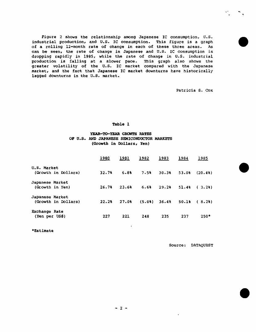
Figure 2 shows the relationship among Japanese IC consumption, U.S. industrial production, and U.S. IC consumption. This figure is a graph of a rolling 12-month rate of change in each of these three areas. As can be seen, the rate of change in Japanese and U.S. IC consumption is dropping rapidly in 1985, while the rate of change in U.S. industrial production is falling at a slower pace. This graph also shows the greater volatility of the U.S. IC market compared with the Japanese market, and the fact that Japanese IC market downturns have historically lagged downturns in the U.S. market.
Patricia S. Cox
Table 1
YEAR-TO-YEAR GROWTH RATES OF U.S. AND JAPANESE SEMICONDUCTOR MARKETS
(Growth in Dollars, Yen)
1980 1981 1982 1983 1984 1985
U.S. Market (Growth in Dollars) 32.7% 6.8% 7.5% 30.3% 53.0% (20.4%)
Japanese Market (Growth in Yen) 26.7% 23.6% 6.6% 29.2% 51.4% ( 3.2%)
J a p a n e s e Marke t (Growth i n D o l l a r s ) 22.2% 27.0% (5.0%) 36.4% 50.1% ( 8.2%)
Exchange Rate (Yen per US$) 227 221 248 235 237 250"
•Estimate
Source: DATAQUEST
- 2 -
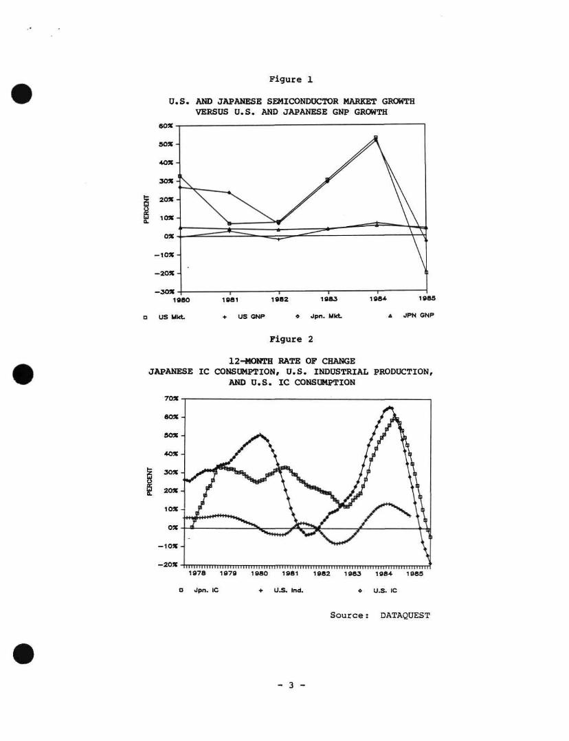
Figure 1
U.S. AND JAPANESE SEMICONDUCTOR MARKET GROWTH VERSUS U.S. AND JAPANESE GNP GROWTH
1980
a US Mkt.
1981 1982 1983
* US GNP « Jpn. MkL
1985
A JPN GNP
Figure 2
12-MONTH RATE OF CHANGE JAPANESE IC CONSUMPTION, U.S. INDUSTRIAL PRODUCTION,
AND U.S. IC CONSUMPTION
iiiiiiIIIIIIiiiniiiiiiiiiiiIirriiIImIuiriiiiiTLiriLiiiimmiiiIijIILIIIIiniiiiiiIiiLur 1978 1979 1980 1981 1982 1983 1964 1985
O <Jpn. IC U.S. Ind. U.S. IC
S o u r c e : DATAQUEST
- 3 -
Dataquest 1 V
JSIS Code: JSIA Newsletters
HITACHI UNVEILS PLAN TO EASE TRADE FRICTION
Hitachi, Ltd., today announced a three-pronged plan aimed at increasing Hitachi's presence in the United States and easing U.S.-Japanese trade friction.
At a Washington, D.c, press conference teleconferenced live to New York, Boston, and Palo Alto, Toshi Kitamura, Hitachi's executive managing director and group executive of the international operations group, outlined the following plans:
In August, an import promotion team headed by Shiro Kawada, executive vice president of Hitachi, Ltd., will begin identifying suppliers and negotiating contracts for exporting U.S. products and services to Japan. The team will spend $120 million between August 1985 and December 1986 in this effort. Hitachi plans to procure $400 million in U.S. goods during 1986 as a result of the program.
Hitachi plans to further expand its extensive manufacturing investment in the United States. Currently, Hitachi operates ten manufacturing plants in five states, including Hitachi Semiconductor (America), Inc., which assembles MOS memory devices. Hitachi directly employs 3,655 people in the United States, of whom 93 percent are U.S. citizens. Three new U.S. plants are planned, to be located in Harrodsburg, Kentucky, Irving, Texas, and at an undisclosed third site.
• Hitachi plans to establish the Hitachi Foundation in the United States with an endowment of $20 million. A prime mission of the Hitachi Foundation will be to promote cultural exchange between Japan and the United States. The foundation will also fund scientific and educational research in the United States.
Mr. Kitamura also announced the appointment of Hiroshi Miyamoto, vice president and corporate secretary of Hitachi America, Ltd., as the first senior representative at Hitachi's soon-to-be-established Washington office for government and corporate affairs.
Mr. Kitamura affirmed Hitachi's belief that free international trade must be maintained and stated that Hitachi has no plans to restrain semiconductor exports to the United States. When questioned about
© 1985 Dataquest Incorporated July 31 ed.-Reproduction Prohibited
Dataquest incorporated, A Subsidiary of A.C, Nielsen Company / 1290 Ridder Park Drive / San Jose, CA 95131 / (403) 971-9000 / Telex 171973
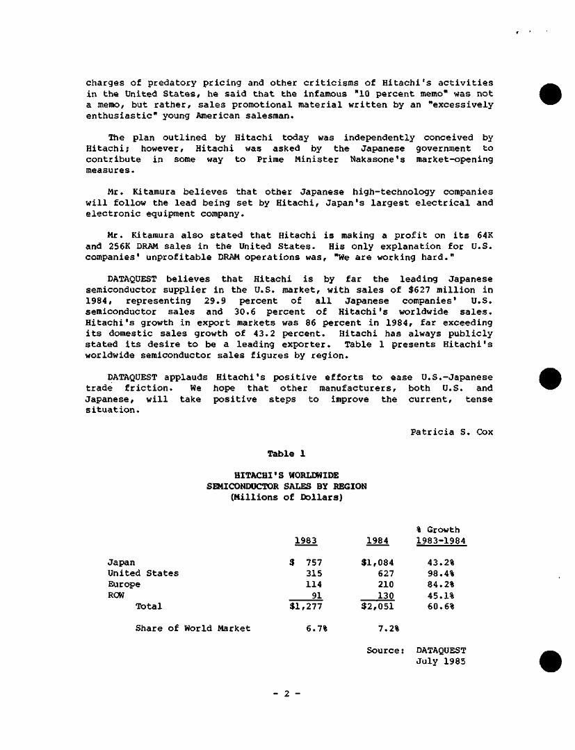
charges of predatory pricing and other criticisms of Hitachi's activities in the United States, he said that the infamous "10 percent memo" was not a memo, but rather, sales promotional material written by an "excessively enthusiastic" young American salesman.
The plan outlined by Hitachi today was independently conceived by Hitachi; however, Hitachi was asked by the Japanese government to contribute in some way to Prime Minister Nakasone's market-opening measures.
Mr. Kitamura believes that other Japanese high-technology companies will follow the lead being set by Hitachi, Japan's largest electrical and electronic equipment company.
Mr. Kitamura also stated that Hitachi is making a profit on its 64K and 256K DRAM sales in the United States. His only explanation for U.S. companies' unprofitable DRAM operations was, "We are working hard."
DATAQUEST believes that Hitachi is by far the leading Japanese semiconductor supplier in the U.S. market, with sales of $627 million in 1984, representing 29.9 percent of all Japanese companies' U.S. semiconductor sales and 30.6 percent of Hitachi's worldwide sales. Hitachi's growth in export markets was 86 percent in 1984, far exceeding its domestic sales growth of 43.2 percent. Hitachi has always publicly stated its desire to be a leading exporter. Table 1 presents Hitachi's worldwide semiconductor sales figures by region.
DATAQUEST applauds Hitachi's positive efforts to ease U.S.-Japanese trade friction. We hope that other manufacturers, both U.S. and Japanese, will take positive steps to improve the current, tense situation.
Patricia S. Cox
Table 1
HITACHI'S WORLDWIDE SEMICONDUCTOR SALES BY REGION
(Millions of Dollars)
Japan United States Europe ROW
Total
Share of World Market
1983
3 757 315 114 91
$1,277
6.7%
1984
$1,084 627 210 130
$2,051
7.2%
Source:
% Growth 1983-1984
43.2% 98.4% 84.2% 45.1% 60.6%
DATAQUEST July 1985
- 2 -
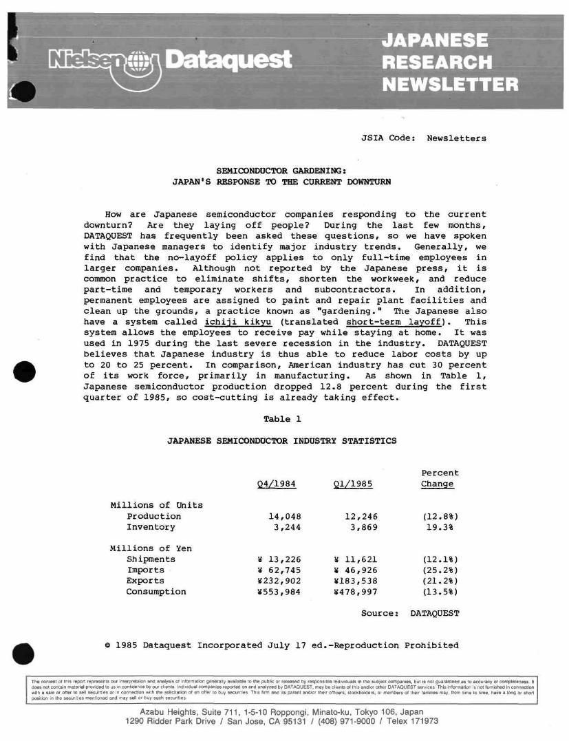
Dataquest JAPANESE RESEARCH NEWSLETTER
JSIA Code: Newsletters
SEMICONDUCTOR GARDENING: JAPAN'S RESPONSE TO THE CURRENT DOWNTURN
How are Japanese semiconductor companies responding to the current downturn? Are they laying off people? During the last few months, DATAQUEST has frequently been asked these questions, so we have spoken with Japanese managers to identify major industry trends. Generally, we find that the no-layoff policy applies to only full-time employees in larger companies. Although not reported by the Japanese press, it is common practice to eliminate shifts, shorten the workweek, and reduce part-time and temporary workers and subcontractors. In addition, permanent employees are assigned to paint and repair plant facilities and clean up the grounds, a practice known as "gardening." The Japanese also have a system called ichiji kikyu (translated short-term layoff). This system allows the employees to receive pay while staying at home. It was used in 1975 during the last severe recession in the industry. DATAQUEST believes that Japanese industry is thus able to reduce labor costs by up to 20 to 25 percent. In comparison, American industry has cut 30 percent of its work force, primarily in manufacturing. As shown in Table 1, Japanese semiconductor production dropped 12.8 percent during the first quarter of 1985, so cost-cutting is already taking effect.
Table 1
JAPANESE SEMICONDUCTOR INDUSTRY STATISTICS
Millions of Units Production Inventory
Millions of Xen Shipments Imports Exports Consumption
Q4/1984
14,048 3,244
¥ 13,226 5f 62,745 ¥232,902 ¥553,984
Ql/1985
12,246 3,869
¥ 11,621 ¥ 46,926 ¥183,538 ¥478,997
Source:
Percent Change
(12.8%) 19.3%
(12.1%) (25.2%) (21.2%) (13.5%)
DATAQUEST
© 1985 Dataquest Incorporated July 17 ed.-Reproduction Prohibited
The content of this report represents our interpretaion and analysis of information generally available to the public or released by responsible individuals in the subject companies, but is not guaranteed as to accuracy or completeness It does not contain material provided to us in confidence by our clients Individual companies reporfed on and analyzed by DATAOUEST, may be clients of this andlor other DATAQUEST services This information is not furnished in connection with a sale or offer to sell securities or in connection with the solicitation of an offer to buy securities This firm and its parent andlor their officers, stockholders, or members of their families may, from time to time, have a long or short position in the securities mentioned and may sell or buy such securities.
Azabu Heights, Suite 711, 1-5-10 RoppongI, IVIinato-ku, Tokyo 106, Japan 1290 Ridder Park Drive / San Jose, CA 95131 / (408) 971-9000 / Telex 171973
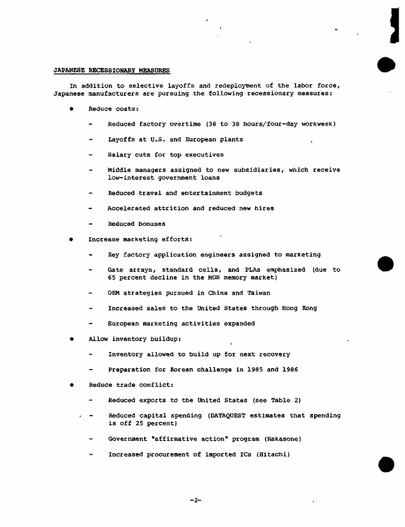
1 JAPANESE RECESSIONARY MEASURES
In addition to selective layoffs and redeployment of the labor force, Japanese manufacturers are pursuing the following recessionary measures:
• Reduce costs:
Reduced factory overtime (36 to 38 hours/four-day workweek)
- Layoffs at U.S. and European plants
Salary cuts for top executives
Middle managers assigned to new subsidiaries, which receive low-interest government loans
Reduced travel and entertainment budgets
Accelerated attrition and reduced new hires
Reduced bonuses
• Increase marketing efforts:
Key factory application engineers assigned to marketing
Gate arrays, standard cells, and PLAs emphasized (due to 65 percent decline in the MOS memory market)
OEM strategies pursued in China and Taiwan
Increased sales to the United States through Hong Kong
European marketing activities expanded
• Allow inventory buildup:
Inventory allowed to build up for next recovery
Preparation for Korean challenge in 1985 and 1986
• Reduce trade conflict;
Reduced exports td the United States (see Table 2)
Reduced capital spending (DATAQUEST estimates that spending is off 25 percent)
Government "affirmative action" program (Nakasone)
Increased procurement of imported ICs (Hitachi)
-2-
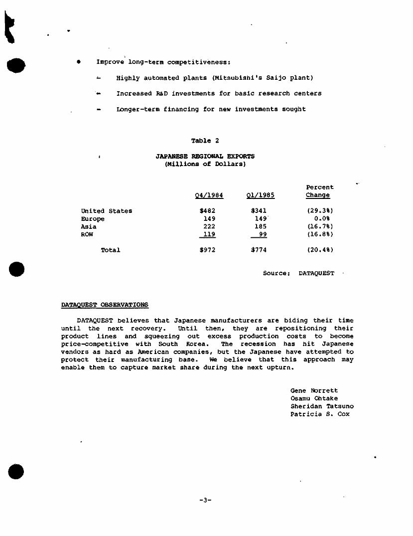
t Improve long-term competitiveness:
Highly automated plants (Mitsubishi's Saijo plant)
** Increased R&D investments for basic research centers
— Longer-term financing for new investments sought
Table 2
JAPANESE REGIONAL EXPORTS (Millions of Dollars)
United States Europe Asia ROW
Total
Q4/1984
$482 149 222 119
Ql/1985
$341 149 185 99
Percent Change
(29.3%) 0.0%
(16.7%) (16.8%)
$972 $774 (20.4%)
Source: DATAQUEST
DATAQUEST OBSERVATIONS
DATAQUEST believes that Japanese manufacturers are biding their time until the next recovery. Until then, they are repositioning their product lines and squeezing out excess production costs to become price-competitive with South Korea. The recession has hit Japanese vendors as hard as American companies, but the Japanese have a t tempted to protect their manufacturing base. We believe that this approach may enable them to capture market share during the next upturn.
Gene Norrett Osamu Ohtake Sheridan Tatsuno Patricia S. Cox
-3-
Dataquest -JAPANESE —
RESEARCH NEWSLETTER
JSIS Code: JSIA Newsletters
THE JAPANESE MARKET: SALES BY ALL MANUFACTURERS IN 1984
SUMMARY
The year 1984 was one of record growth in the Japanese semiconductor industry, record sales by companies worldwide, and large opportunities for foreign suppliers—especially U.S. companies—to capitalize on a booming Japanese market.
Our data show that overall, Japanese companies sacrificed high growth in their home market—which grew 50.1 percent in 1984—in order to achieve phenomenally high growth in overseas markets. Sales by Japanese suppliers grew only 49.0 percent in their home market, while their worldwide sales increased 60.8 percent. At the same time, U.S. companies' sales in Japan grew 65.2 percent, higher than their worldwide growth of 44.9 percent. Sales in Japan by European and Rest of World companies grew 25.5 percent versus 36.8 percent worldwide and 23.0 percent versus 23.6 percent worldwide, respectively. All data in this newsletter are stated in terms of U.S. dollars.
TOTAL SEMICONDUCTOR
Table 1 lists 1984 sales in Japan of integrated circuits, discretes, and optoelectronics, by the leading suppliers to the Japanese market. Leading the list as the top five suppliers are NEC, Toshiba, Hitachi, Matsushita, and Mitsubishi. Texas Instruments, Number 7, is the only non-Japanese company in the top ten, with total 1984 sales of $344 million. It is also interesting to note that TI is one of the top ten producers of semiconductors in Japan, with 1984 production of approximately $400 million.
® 1985 Dataquest Incorporated June 28 ed.-Reproduction Prohibited
The content of this report represents our interpretaion and analysis of information generally available to the public or released by responsible individuals In the subject companies, but is not guaranteed as to accuracy or completeness It does not contain material provided to us in confidence by our clients Individual companies repoded on and analyzed by DATAQUEST, may be clients of this and/or other DATAQUEST services This intormation is not furnished in connection with a sale or offer to sell securities or in connection with the solicitation of an offer to buy securities This firm and its parent and/or their officers, stockholders, or members of their families may, from time to time, have a long or short position in the securities mentioned and may sell or buy such securities
Azabu Heights, Suite 711, 1-5-10 RoppongI, MInato-ku, Tokyo 106, Japan 1290 Bidder Park Drive / San Jose,. CA 95131 / (408) 971-9000 A Telex 171973
Japanese companies held 87.6 percent of their home market in 1984, a drop of 0.8 percentage points from 1983, while U.S. companies gained 1 percentage point, to hold 11.4 percent of the Japanese market (see Figure 1) . Table 2 lists 1982 through 1984 Japanese total semiconductor sales for the leading suppliers, plus yearly growth rates. Companies exhibiting phenomenal growth include AMD, growing 176.2 percent to overtake National Semiconductor, General Instrument, Fairchild, and Signetics; Harris, growing 80;0 percent; and MMI, growing 200.0 percent.
Total Integrated Circuit
Figure 2 shows the geographic split by company base for sales of ICs in Japan. In this arena, U.S. companies enjoy their highest market share, 14.0 percent. Because of their relatively high concentration of discrete sales in Japan, Japanese suppliers hold only 85.4 percent of the Japanese IC market.
Table 3 lists sales in Japan by the leading IC suppliers to that market.
Total Bipolar Digital
Figure 3 shows the geographic split by company home base for bipolar digital IC sales in Japan. U.S. companies hold 33 percent of this market, which is the largest U.S. market share in the Japanese semiconductor market. U.S. companies' bipolar digital sales in Japan grew 71.2 percent versus worldwide growth of 60.4 percent. Japanese companies' bipolar digital IC sales in Japan grew 28.4 percent, while the Japanese market grew 39.9 percent. Thus, U.S. companies gained significant market share in this field, picking up 6 percentage points in one year.
Table 4 lists the leading bipolar digital suppliers to the Japanese market. The Number 2 supplier is TI, with 1984 sales of $180 million.
Total MOS
As shown in Figure 4, U.S. companies held 10.5 percent of the Japanese MOS market in 1984, while Japanese companies held 89.3 percent, and European companies had only 0.2 percent. Amazingly, U.S. companies' growth in Japan was 86.3 percent, considerably larger than their worldwide growth of 52.6 percent. Growth by Japanese companies in Japan was 71.7 percent, less than their 76.4 percent growth worldwide; this is because Japanese companies concentrated their MOS sales heavily in export markets—44 percent of all Japanese MOS production was exported in 1984.
Table 5 lists MOS revenues of the leading suppliers to the Japanese market. Intel and TI are the only foreign companies among the top ten, with MOS sales of $103 million and $100 million, respectively.
2 -
Linear
U.S. companies' sales of linear ICs in Japan grew 46.0 percent in 1984, higher than their worldwide growth of 34.1 percent. Japanese companies, on the other hand, experienced growth in Japan of only 39.0 percent, lower than their worldwide growth of 45.3 percent. We attribute these facts to the increasing Japanese demand for high-end, industrial linear ICs, in which U.S. linear suppliers excel, coupled with high Japanese exports of consumer linear ICs to Asia.
Figure 5 shows that U.S. companies held 10.8 percent of the 1984 Japanese linear market, Japanese companies held 88.2 percent, and all others held l.O percent. Table 6 lists Japanese linear revenues by the leading suppliers to the Japanese market. Three U.S. companies—TI, National Semiconductor, and Analog Devices—number among the top ten. We believe that about 30 percent of the Japanese linear market is supplied by a very large number of relatively small Japanese companies.
Discretes and Optoelectronics
Figure 6 shows that U.S., European, and Rest of Wbrld suppliers hold only 5.7 percent of the Japanese discrete market, while Japanese suppliers have a 94.3 percent market share. Table 7 lists the leading suppliers to the market.
Similarly, U.S., European, and Rest of World companies have only 5.7 percent of the Japanese optoelectronics market, as shown in Figure 7, while Japanese companies hold 94.3 percent of the market. Table 8 lists the top suppliers to the Japanese optoelectronics market, which is heavily dominated by the three leaders—Sharp, Matsushita, and Toshiba.
CONCLUSION
The Japanese semiconductor market remained the province of Japanese manufacturers, dominated by the big nine, in 1984. The European and Rest of World presence was hardly felt, accounting for less than 1 percent of the total market. U.S. companies picked up a small amount of market share, as a result of massive Japanese exports diverting potential domestic sales to overseas markets (i.e., the exports left a partial void, which the U.S. companies filled).
As Japan/world trade tension heats up, we believe that Japanese industry as a whole, and electronics in particular, will be forced to open its domestic markets to more foreign goods. One portent of this is Hitachi's recent announcement that it plans to increase its procurement of foreign-produced semiconductors from 1 percent of total procurement to 5 percent during the current fiscal year. We believe that policies like this could lift the "12 percent barrier" that many U.S. suppliers believe exists (so that the future U.S. share of the Japanese semiconductor
- 3 -
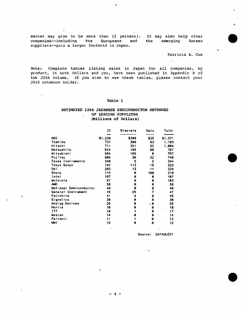
market may grow to be more than 12 percent) companies—including the Europeans and suppliers—gain a larger foothold in Japan.
It may also help other the emerging Korean
Patricia S. Cox
Note: Complete tables listing sales in Japan for all companies, by product, in both dollars and yen, have been published in Appendix B of the JSIA volume. If you wish to see these tables, please contact your JSIS notebook holder.
Table 1
ESTIMATED 1 9 8 4 JAPANESE SEMICONDUCTOR REVENUES OF LEADING SUPPLIERS ( M i l l i o n s o f D o l l a r s )
NEC Tosh I bo HI tochI Motsushi to M l tsubi sh i Fuj i tsu Texos Instruments Tokyo Sanyo Oki Sharp I n t e l Motoro la AMD Not iona l Sein I conductor General Instrument Fa I r c h i I d SIgnet ics Ana log Devices Horr i s ITT Mostek Fe r rant i MMI
IC
$1 ,238 731 711 524 584 686 346 192 203 115 107 97 58 49 15 41 30 26 18 16 14 11 12
Discre te
$308 309 351 195 165 30
2 113
13 0 0 6 0 0
25 4 0 0 0 1 0 1 0
Opto Total
$25 $1,571 63 22 68
8 32
2 16 11
100 0 0 0 0 7 0 0
. 0 0 0 0 0 0
1,103 1,084
787 757 748 344 322 224 215 107 103 58 49 47 45 30 26 18 17 14 12 12
Source: DATAQUEST
- 4
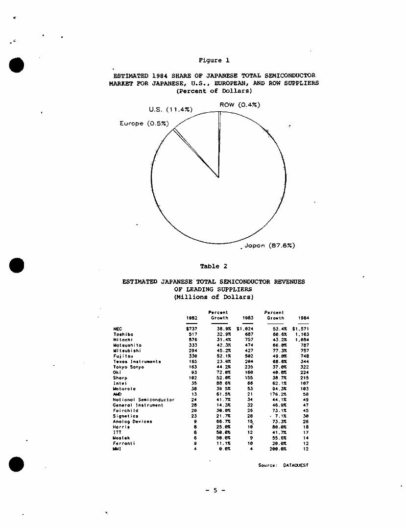
Figure 1
ESTIMATED 1984 SHARE OF JAPANESE TOTAL SEMICONDUCTOR MARKET FOR JAPANESE, U.S., EUROPEAN, AND ROW StJPPLIERS
(Percent of Dollars)
U.S. (1 1.4%)
Europe (0.5%)
ROW (0.4%)
Japan (87.6%)
Table 2
ESTIMATED JAPANESE TOTAL SEMICONDUCTOR REVENUES OF LEADING SUPPLIERS (Millions of Dollars)
NEC Toshiba H i tachi kiIatsushi ta Mi tsubishi Fuj i tsu Texas Instruments Tokyo Sanyo Oki Shorp I n t e l MotoroIa AMD No t iona l Semiconductor GeneroI Instrument Fai rch i Id Signet ics AnaIog Devices Ho r r i s ITT litostek Ferront i luMI
1982
$737 517 576 333 294 330 165 163 93
102 35 38 13 24 28 20 23
9
e e 6 9 4
Percen t Growth
38.9% 32.955 31 .4% 42.3% 45. 2X 52.1J5 23.65! 44. 2J! 72.05J 52.055 88.655 39 555 61 .55! 41 .75! 14.35! 30.0?: 21 .7X 66.75! 25.05! 50.055 50.055 11.15! 0.05!
1983
$1 .024 687 757 474 427 502 204 235 160 155 66 53 21 34 32 26 28 15 10' 12 9
10 4
Percent Growth
53.4X 60.65! 43.25! 66.05! 77.35! 49.05! 68.65! 37.05! 40.05! 38.75! 62.15! 94.35!
176.25! 44.1% 46.955 73.15!
• 7 . I X 73.35! 80.05! 41 .75! 55.65! 20.05!
200.055
1984
$1 ,571 1 .103 1 .084
787 757 748 344 322 224 215 107 103 58 49 47 45 30 26 18 17 14 12 12
Source: OATAOUEST
- 5 -
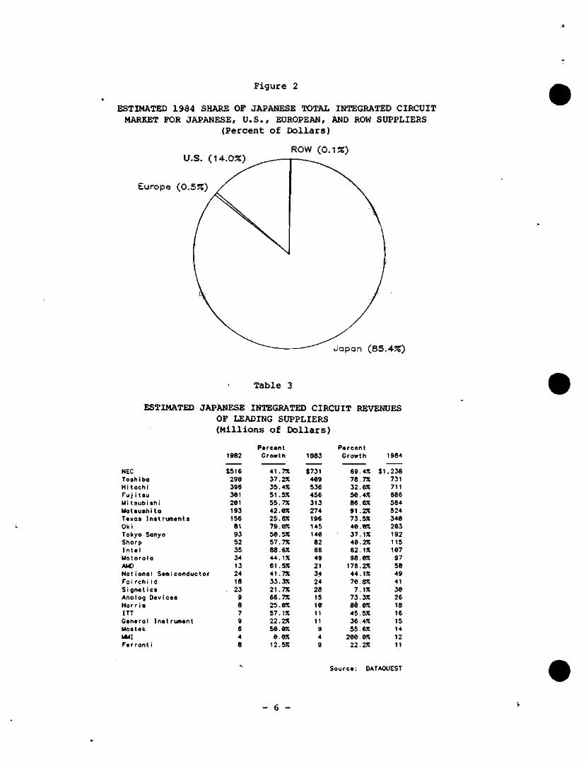
Figure 2
ESTIMATED 1984 SHARE OF JAPANESE TOTAL INTEGRATED CIRCUIT MARKET FOR JAPANESE, U.S., EUROPEAN, AND ROW SUPPLIERS
(Percent of Dollars)
U.S. (14.0%) ROW (0.1%)
Europe (0 .5%)
Japan (85 .4%)
Table 3
ESTIMATED JAPANESE INTEGRATED CIRCUIT REVENUES OF LEADING StJPPLIERS (Millions of Dollars)
NEC Tosh!bo
Hitachi
Fuj i tsu
Uitsubishi Matsushi to
Texas Instruments
Ok! Tokyo Sanyo
Sharp
Intel
Motorola
AMD Nat lona I Semiconductor Foi rchi Id S i g n e t ics
AnoIog Devices H o r r i s
ITT GeneroI Instrument Mostek
ItMI
Ferrant i
1982
$516 298 396 jei 201 193 156 81 93 52 35 34 13 24 18
, 23 9 8 7 9 6 4 8
Percent Growth
41.7J!
37.25!
35. 4J!
51.5%
55.7%
42.0%
25.6%
79.0%
50.5%
57.7%
88.6%
44.1% 61.5% 41.7% 33.3% 21.7% 66.7% 25.0% 57.1% 22.2% 50.0% 0.0% 12.5%
1983
$731 409 536 456 313 274 196 145 140 82 66 49 21 34 24 28 15 10 11 11 9 4 9
Percent Growth
69.4% 78.7% 32.6% 50.4% 86.6% 91 .2% 73.5% 40.0% 37.1% 40.2% 62.1% 98.0% 176.2% 44.1% 70.8% 7.1%
73.3% 86.0% 45.5% 36.4% 55.6%
200.0% 22.2%
1984
$1,238 731 711 686 584 524 340 203 192 115 107 97 58 49 41 30 26 18 16 15 14 12 11
Source: DATAQUEST
- 6 -
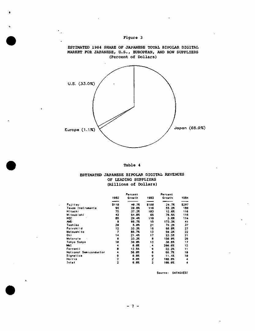
Figure 3
ESTIMATED 1984 SHARE OF JAPANESE TOTAL BIPOLAR DIGITAL MARKET FOR JAPANESE, U.S., EUROPEAN, AND ROW SUPPLIERS
(Percent of Dollars)
U.S. (33.0%)
Europe (1.1%) Japan (65.9%)
Table 4
ESTIMATED JAPANESE BIPOLAR DIGITAL REVENUES OF LEADING SUPPLIERS (Millions of Dollars)
Fuj1tsu Texas Instruments Hitachi Mi tsubi Shi NEC AMD Toshiba Fai rchi I d Matsushi to OI(i Motor© I a Tokyo Sanyo lAII Ferrant i Notional Semiconductor Signet ics Horr i s Intel
1982
$118 96 75 42 85 9
20 12 7 14 6 ie 4 8 4 9 2 2
Percent Growth
48.7X 20.8% 37.3% 54.8SJ 29.4% 66.7%
5.0% 33.3% 85.7% 21.4% 33.3% 36.0%
e.e% 12.5% 50. e% 0.0% 0.0% 0.0%
1983
$166 116 103 65 110 15 21 16 13 17 8 13 . 4 ' 9 6 9 2 2
Percent Growth
24.7% 55.2% 12.6% 78.5% 3.6%
173.3% 76.2% 68.8% 69.2% 23.5% 150.0% 30.8%
200.0% 22.2% 66.7% 11.1%
100.0% 100.0%
1984
$207 180 116 116 114 41 37 27 22 21 20 17 12 11 10 10 4 4
Source: DATAOUEST
- 7
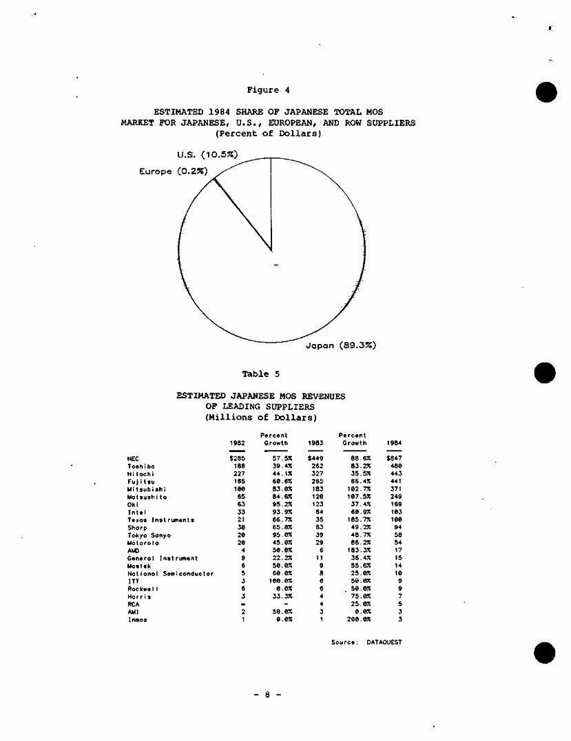
Figure 4
ESTIMATED 1984 SHARE OF JAPANESE TOTAL MOS MARKET FOR JAPANESE, U.S., EUROPEAN, AND ROW SUPPLIERS
(Percent of Dollars)
U.S. (10.5%)
Europe (0.2%)
Japan (S9.3%)
Table 5
ESTIMATED JAPANESE MOS REVENUES OF LEADING SUPPLIERS (Millions of Dollars)
NEC Toshiba H i tachi Fuj i tsu Mi tsubi Shi MatsushIto Oki In te I Texas Instruments Shorp Tol<yo Sonyo Motoro la AMD GeneraI Instrument Mostek NationaI Semiconductor ITT RockweI I Ha r r i s RCA AMI Inmos
1982
$285 188 227 165 lee 65 63 33 21 38 20 2e
4 9 6 5 3 6 3
—. 2 1
Percent Growth
57.5J! 39 . 4J! 44.15! 6e.6% 83.e;s 84.6% 95.255 93 . 9J: 66.755 65.855 95.05! 45.055 50.055 22.255 50.055 60.055
100.055 0.0%
33.35!
-50.05!
0.05!
1983
$449 262 327 265 183 120 123 64 35 63 39 29
6 11 9 8 6 6 4 4 3 1
Percen t Growth
88.65! 83.25! 35.55! 66.45!
102.7% 107.5%
37.4% 60.9%
185.7% 49.2% 48.7% 86.2%
183.3% 36.4% 55.6% 25.0% 50.0% 50.0% 75.0% 25.0%
0.0% 200.0%
1984
$847 480 443 441 371 249 169 103 100 94 58 54 17 15 14 10 9 9 7 5 3 3
Source: DATAOUEST
- 8 -
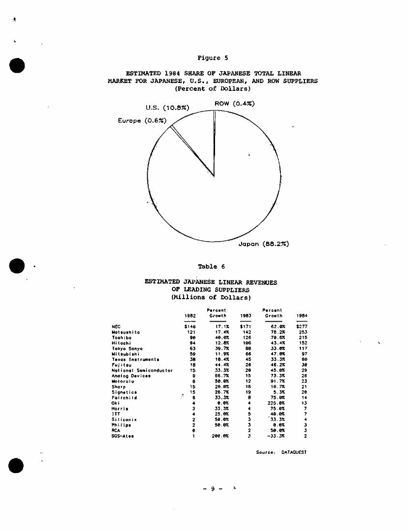
Figure 5
ESTIMATED 1984 SHARE OF JAPANESE TOTAL LINEAR MARKET FOR JAPANESE, U.S., EUROPEAN, AND ROW SUPPLIERS
(Percent of Dollars)
U.S. (10.8%)
Europe (0.6%)
ROW (0.4%)
Japan (88.2%)
Table 6
ESTIMATED JAPANESE LINEAR REVENUES OF LEADING SUPPLIERS (Millions of Dollars)
NEC Matsuslii to Tosliiba Hitachi Tokyo Sanyo Mi tsubishi Texas Instruments Fuj i tsu Na t iona I Semiconductor AnoIog Devices MotoroIa Sharp Signet ics Fai rchi Id Oki Horr is ITT Si 1 icon!X Phi 1ips RCA SGS-Ates
1982
$146 121 90 94 6J 59 3B 18 15 9 8 15 15 6 4 3 4 2 2 0 1
Percent Growth
17.15! 17.4?! 40.0% 12.8X 39.75! 11.9% 18.4% 44.4% 33.3% 66.7% 50.0% 20.0% 26.7% 33.3% 0.0%
33.3% 25.0% 50.0% 50.0%
200.0%
1983
$171 142 126 106 88 66 45 26 20 15 12 18 19 8 4 4 5 3 3 2 3
Percent Growth
62.0% 78.2% 70.6% 43.4% 33.0% 47.0% 33.3% 46.2% 45.0% 73.3% 91 .7% 16.7% 5.3%
75.0% 225.0% 75.0% 40.0% • 33.3% 0.0%
50.0% -33.3%
1984
$277 253 215 152 117 97 60 38 29 26 23 21 20 14 13 7 7 4 3 3 2
Source: DATAOUEST
- 9 -
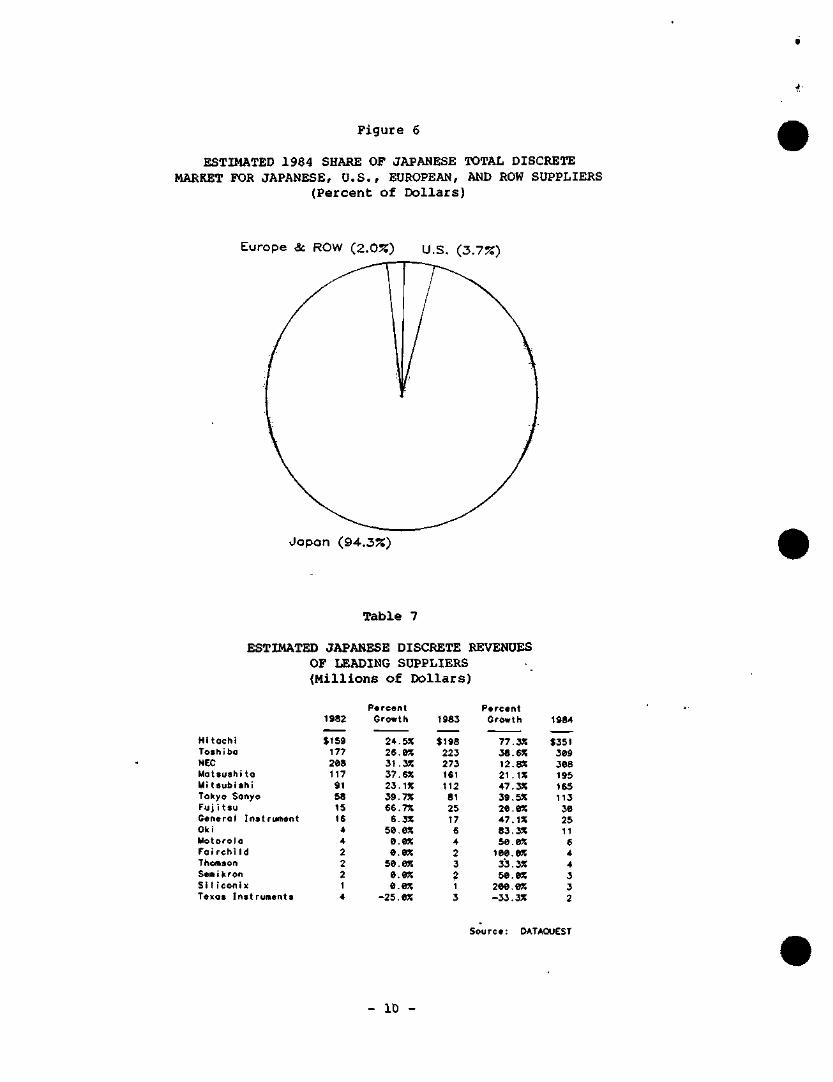
Figure 6
ESTIMATED 1984 SHARE OF JAPANESE TOTAL DISCRETE MARKET FOR JAPANESE, U.S., EUROPEAN, AND ROW SUPPLIERS
(Percent of Dollars)
Europe &. ROW (2.0%) U.S. (3.7%)
Japan (94.3%)
Table 7
ESTIMATED JAPANESE DISCRETE REVENUES OF LEADING SUPPLIERS (Millions of Dollars)
Hitachi Toshiba NEC Matsushi ta Mi tsubiahi Tokyo Sanyo Fuj f tsu GeneraI Instrument Oki IttotoroIc Fai rchi Id Thomson Semi kron Si t iconi X Texas Instruments
1982
$159 177 208 117 91 58 15 16 4 4 2 2 2 1 4
Percent Growth
24.5X 26. e^ 31.3X
37. ex 23.155 39.75! 66.75! 6.35!
50.05! 0.05! 0.05!
50.05! 0.05; 0.05!
-25 .05!
1983
$198 223 273 161 112 81 25 17 6 4 2 3 ? 1 3
Percent Growth
77.35! 38.6X 12.855 21 .15! 47.35! 39.5X 20.05! 47.15! 83.355 50.0%
100.BX 33.35! 50.05!
200.05! -33.35!
1984
$351 309 308 195 165 113 30 25 11 6 4 4 3 3 2
Source: OATAOUEST
ID -
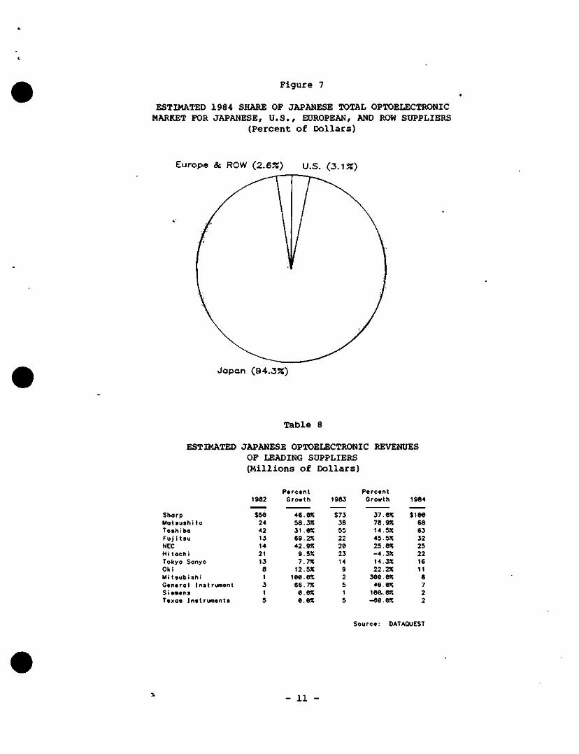
Figure 7
ESTIMATED 1984 SHARE OF JAPANESE TOTAL OPTOELECTRONIC MARKET FOR JAPANESE, U.S., EUROPEAN, AND ROW SUPPLIERS
{Percent of Dollars)
Europe <Se ROW (2.6%) U.S. (3.1%)
Japan (94.3%)
Table 8
ESTIMATED JAPANESE OPTOELECTRONIC REVENUES OF LEADING SUPPLIERS (Millions of Dollars)
Sharp Matsushi ta Toshiba Fuj i tsu NEC Hitochi Tokyo Sanyo Oki Mi tsubi Shi General Ins Si emens Texas Instr
t rument
uments
1982
$5e 24 42 13 14 21 13 8 1 3 1 5
Percent Growth
46.0% 58.3J! 31 .ex 69.2% 42.9% 9.5% 7.7% 12.5% iee.e% 66.7% e.e% e.e%
1983
$73 38 55 22 20 23 14 9 2 5 1 5
Percent Growth
37.8% 78.9% 14.5% 45.5% 25. e% -4 .3% 14.3% 22.2%
3ee.e% 40. e% iea.e% -60.0%
1984
$100 68 63 32 25 22 16 11 8 7 2 2
Source: DATAQUEST
- 11 -
Dataquest RESEARCH BULLETIN
JSIA Code: Newsletters
U.S.-JAPAN SEMICONDUCTOR TRADE UPDATE FIRST QUARTER 1985
The global semiconductor slump is severely cutting into sales by U.S. and Japanese semiconductor suppliers in each other's markets. DATAQUEST believes that U.S. companies are losing market share in Japan and that Japanese manufacturers are faring even worse in the U.S. market. We see the following situations:
• U.S. sales in Japan were down 16.5 percent in the first quarter of 1985 from the fourth quarter of 1984, while the Japanese market fell 14.3 percent. At the same time, Japanese sales in the United States fell 29.1 percent in the first quarter of 1985, while the U.S. market dropped 19.5 percent.
• Japanese companies, which gained more than three percentage points of market share in the United States in 1984 due to their dominance in the MOS memory market, are paying for that now as the market drops precipitously. We believe that the Japanese share of the U.S. semiconductor market was only 12.5 percent in the first quarter of 1985.
• Inventories of imported finished goods are high, expecially in the United States. We believe that many parts are being sold at very low margins in order to deplete inventory.
• Because of the reduced semiconductor trade between the United States and Japan, the U.S. deficit has also been reduced, to $155 million in the first quarter of 1985, from $261 million in the fourth quarter of 1984.
Table 1 shows semiconductor sales in Japan by U.S. companies and semiconductor sales in the United States by Japanese companies. Figure 1 shows quarterly semiconductor trade between the United States and Japan from first quarter 1983 to the first quarter of 1985. All numbers used in this newsletter are DATAQUEST's estimates of actual sales of finished goods by U.S.-based companies and Japanese-based companies in each Other's markets.
Patricia S. Cox
© 1985 Dataquest Incorporated July 10 ed.-Reproduction Prohibited
Tne conlen I o( Ihis reooi
provided icfus in t ontit lei
jrally avaiialile lo ine pul
d tjy DATAQUFST m.iy h • r o'hKi DATAQUEST sc-v
s firm and it's p.i 'pni .
: suD(Hcl companies out is not gu.
Dataquest Incorporated, A Subsidiary of A.C. Nielsen Company / 1290 Bidder Park Drive / San Jose, CA 95131 / (408) 971-9000 / Telex 171973
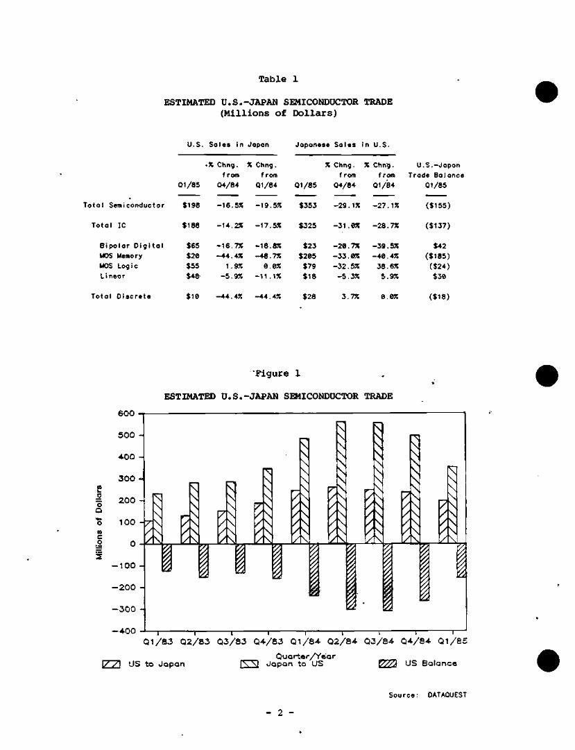
Table 1
ESTIMATED U.S.-JAPAN SEMICONDUCTOR TRADE (Mi l l ions o f Do l lars)
Tota l Semiconductor
Toto l IC
U.S. Sales In Japon
•% Chng. X Chng. from from
01/85 04/84 01/84
Japanese Sa les in U.S.
$198
$188
-16.5% -19.5%
-14.2J! -17.5%
Q1/85
$353
$325
% Chng. % Chn'g. U.S.-Japan
from from Trade Balance
04/84 01/84 01/85
-29.1% -27.1%
-31.0% -28.7%
($155)
($137)
Bipolar D ig i ta l $65 MOS Memory $20 MOS Logic $55 Linear $48-
-16 .7% -18.8% $23 -44.4% -48.7% $205
1.9% 0.0% $79 -5 .9% - 1 1 . 1 % $18
-20 . 7% -39 .5% $42 -33 .0% -40 .4% ($185) -32 .5% 36.6% ($24 )
- 5 . 3 % 5.9% $30
Tota l D i s c r e t e $ 1 0 - 4 4 . 4 % - 4 4 . 4 % $28 3.7% 0.0% ($18)
'Figure 1
ESTIMATED U.S.-JAPAN SEMICONDUCTOR TRADE
600
o
o 03
C
o
500 -
400 -
3OO
200 -
100 -
O
-1OO -
-200 -
-300
I 5 \ Z>
I I
^
I I i J
^ ^
I i
R^ / \ ^ \
M ,
-4OO -J 1 -1 [ 1 1 [ Q1/S3 Q2/8J Q3/SJ Q4/S3 Q1/84 Q2/84
I I
1771 us to Japan Quarter/Year
F V ^ J a p a n t o U S
1 1 r Q 3 / S 4 Q 4 / S 4 Q l / S S
fTPZ^ US Ba lance
Sou rce: DATAQUEST
- 2 -
JSIA Code: Newsletters
JAPANESE SEMICONDUCTOR TECHNOLOGY TRENDS First Quarter 1985
SUMMARY
The outpouring of Japanese papers at the 1985 International Solid State Circuits Conference (ISSCC) was the highlight for the first quarter of 1985. As discussed in our newsletter dated March 18, 1985, "Japan Takes Center Stage at ISSCC 1985," Japanese research teams presented 44 percent of all papers presented at the conference. However, the announcement of 1Mb DRAMs and 256K SRAMs only signals the beginning of the race for the next-generation devices. DATAQUEST notes the following developments in Japanese semiconductor technology:
m Opening and expansion of corporate basic research centers (Konishiroku Photo, Matsushita, Mitsubishi, Oki, Sanyo, Sharp, Tokyo Electron, Toshiba)
• Shift to submicron processes and 3-dimensional structures (multilevel memory cells and stacked capacitor cells) for 4Mb and 16Mb DRAMs)
• Triple-layer polysilicon and hot electron technology (Toshiba's "flash" EEPRQM)
• Joint development of original MPU software development tools (Hitachi/Sophia and NEC/Sophia)
• Emergence of GaAs gate arrays as a stepping-stone to GaAs digital ICs (Oki, Toshiba)
• Introduction of standard cell methods and libraries (Mitsubishi, NEC, Ricoh)
• Heated competition to open ASIC design centers and develop PC-based workstations
Accelerating research in semiconductor lasers optically based Information Network System (INS) value-added networks (VAN)
for NTT's and private
© 1985 Dataquest Incorporated June 21 ed.-Reproduction Prohibited
The content of this report represents our interpretaion and analysis of information generally available to the public or released by responsible individuals in the subject companies, but is not guaranteed as to accuracy or completeness It does not contain material provided to us in confidence by our clients Individual companies reported ori and analyzed by DATAQUEST, may be clients of this and/or other DATAQUEST services This information is not furnished in connection with a sale or offer to sell securities or in connection with the solicitation of an offer to buy securities This firm and its parent and/or their officers, stockholders, or members of their families may, from time to time, have a long or short ljosJiion in the securities menticndd and may sell or buy such socurities
Azabu Heights, Suite 711, 1-5-10 Roppongi, Minato-ku, Tokyo 106, Japan 1290 Ridder Park Drive / San Jose, CA 95131 / (408) 971-9000 / Telex 171973
• Reductions in GaAs wafer defect densities (Hitachi, MITI Optoelectronics Project, NTT, Show Denko, Sumitomo Metal Mining, Tohoku University)
• Development of laser CVD or defect corrections (NEC) and laser recrystallization for 3-dimensional silicon-on-insulator (Mitsubishi)
• Introduction of water-soluble photopolymer resists (Matsushita/ Hayashibara) and molybdenum silicide photomask materials for 4Mb and over
GOVERMMENT R&D PROJECTS
DATAQUEST staff visited MITI's New Semiconductor Functions Elements Project (1981-1990), their Supercomputer Project (1981-1990), their Light Reactive Project, and finally, NTT's Atsugi Laboratory. The following are highlights of our discussions with their project managers.
MITI's New Semiconductor Functions Elements Project
Shigeru Fukuda, project manager, pointed out that the project is organized as shown in Figure 1. A committee of university professors is advising MITI's Agency for Industrial Science and Technology (AIST) on basic research. There are approximately 300 corporate researchers assigned to the project, equally divided among the three areas. Major results of the project to date include:
• MBE for AlGaAs/GaAs—Fujitsu has increased crystal perfection, and decreased alloy clusters (117,000 square cm/v sec at 77 degrees Kelvin)
• MBE for InGaAs/GaSb—Sumitomo has achieved 7,200 square cm/v sec at room temperature
• MBE for silicon—Hitachi has developed a formation of p-n doping superlattice structures and silicon-nickel electrodes.
• MOCVD for AlGaAs/GaAs—Sony has investigated heterostructure abruptness (32-46 angstroms) and developed an impurity high doping technique that permits high-speed growth.
DATAQUEST believes that the New Functions Project is MITI's VLSI Project for the 1980s. The next major breakthroughs in semiconductor technology will come in the areas of 3-dimensional ICs (e.g., Mitsubishi's 1Mb DRAM with 3-dimensional stacked capacitor cells and Hitachi's 4-bit, 16-level cell storage for the file memory) and III-V compound superlattice devices. We will update you on the latest developments after the project's annual symposium in July.
- 2 -
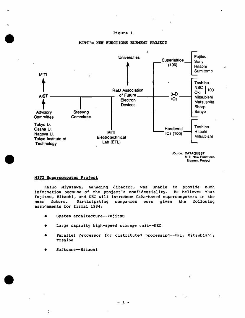
F i g u r e 1
MITI'S NEW FUNCTIONS ELQIENT PROJECT
MITI
t AIST
t Advisory Committee
Tokyo U. Osaha U. Nagoya U. Tokyo Institute of Technology
Steering Committee
Universities
i L
M
R&D Association of Future Electron Devices
Tl Electrotechnical
Lab (ETL)
Superlattice (100)
Fujitsu Sony Hitachi Sumitomo
3-D ICs
100
Hardened ' iCs (100)'
Source:
Toshiba NSC Oki Mitsubishi Matsushita Sharp Sanyo
Toshiba Hitachi Mitsubishi
DATAQUEST MITI New Functions
Element Project
MITI Supercomputer Project
Kazuo Miyazawa, managing director, was unable to provide much information because of the project's confidentiality. He believes that Fujitsu, Hitachi, and NEC will introduce GaAs-based supercomputers in the near future. Participating companies were given the following assignments for fiscal 1984:
• System architecture—Fujitsu
• Large capacity high-speed storage unit—NEC
• Parallel processor for distributed processing—Oki-, Mitsubishi, Toshiba
• Software—Hitachi
- 3 -
• Josephson junction—Fujitsu, Hitachi, NEC
• High electron mobility transistors (HEMT)—Fujitsu, Oki
• GaAs—Mitsubishi, NEC, Toshiba
For results of these projects, see the Technology Development and New Product Announcements sections of this and previous JSIS Technology Trends newsletters (April 5, 1984; August 17, 1984; October 26, 1984; January 23, 1985).
MITI Light Reactive Material Project
In January, MITI organized a $40 million project to develop high-performance photochromic materials and other materials that alter magnetic or light refraction when exposed to light. The goal is to develop materials for voice, image, and computer storage systems. Hitachi, Mitsubishi Electric, and Toshiba are likely candidates among the 5 to 10 firms that will be selected. Other candidates include Mitsubishi Chemical Research Centers.
NTT Atsuqi Lab
Dr. Sudoh, semiconductor research manager, explained that the Atsugi Lab has the latest experimental semiconductor equipment from Japanese equipment makers. NTT is pursuing four processes: plasma x-ray using the synchrotron at the Tsukuba High Physics Lab; 0.1-micron level electron beam; submicron stepping; and plans for excimer lasers. NTT is interested in long-term joint research with foreign companies (e.g., Eaton for ion implant equipment and Energy Conversion Devices for memory). Companies interested in joint research should contact NTT New York City or Los Altos, California (Silicon Valley). NTT is also pursuing wafer scale integration at the Musashino Lab for memory-level application, but not at the logic level.
CORPORATE R&D
In January, Japanese companies highlighted their research achievements in 1984 and goals for 1985. As shown in Table 1, the major companies are pursuing basic research in 1985.
- 4 -
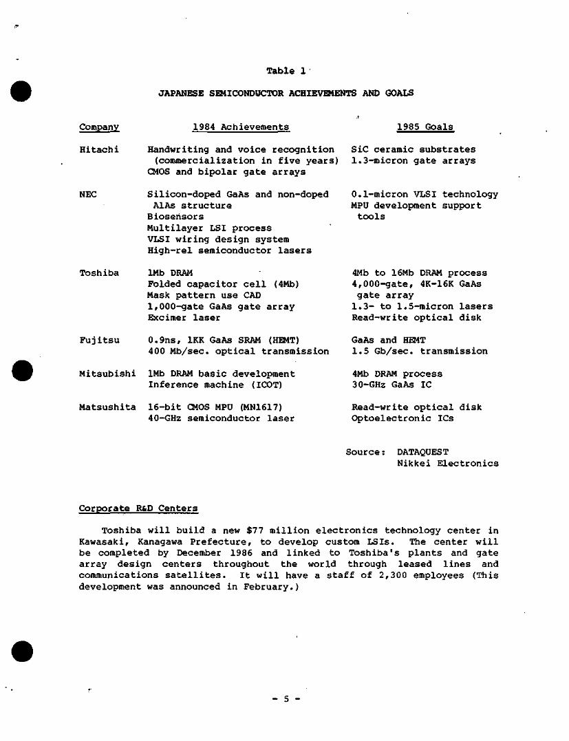
Table 1
JAPANESE SEMICONDUCTOR ACHIEVEMENTS AND GOALS
Company 1984 Achievements
Hitachi Handwriting and voice recognition (commercialization in five years)
CMOS and bipolar gate arrays
NEC Silicon-doped GaAs and non-doped AlAs structure Bioseiisors Multilayer LSI process VLSI wiring design system High-rel semiconductor lasers
Toshiba 1Mb DRAM Folded capacitor cell (4Mb) Mask pattern use CAD 1,000-gate GaAs gate array Excimer laser
Fujitsu 0.9ns, IKK GaAs SRAM (HEMT) 400 Mb/sec. optical transmission
Mitsubishi 1Mb DRAM basic development Inference machine (ICOT)
Matsushita 16-bit CMOS MPU (MN1617) 40-GHz semiconductor laser
1985 Goals
SiC ceramic substrates 1.3-micron gate arrays
0.1-micron VLSI technology MPU development support tools
4Mb to 16Mb DRAM process 4,000-gate, 4K-16K GaAs gate array 1.3- to 1.5-micron lasers Read-write optical disk
GaAs and HEMT 1.5 Gb/sec. transmission
4Mb DRAM process 30-GHz GaAs IC
Read-write optical disk Optoelectronic ICs
Source: DATAQUEST Nikkei Electronics
Corporate R&D Centers
Toshiba will build a new $77 million electronics technology center in Kawasaki, Kanagawa Prefecture, to develop custom LSIs. The center will be completed by December 1986 and linked to Toshiba's plants and gate array design centers throughout the world through leased lines and communications satellites. It will have a staff of 2,300 employees (This development was announced in February.)
- 5 -
NEW INDUSTRY ASSOCIATIONS
In March, 350 Japanese companies formed the Japanese Semiconductor Equipment and Materials Association. The association has as its director Mr. Yoshida, director of Nikon and a speaker at our April 14-15 conference in Hakone.
TECHNOLOGY DEVELOPMENTS
With the rapid decline in 256K DRAM prices, the megabit DRAM era is in full swing. Five Japanese companies introduced 1Mb DRAM papers at ISSCC 1985 (Fujitsu, Hitachi, Mitsubishi, NEC, and Toshiba), in addition to AT&T, IBM, and Mostek. (See our JSIS newsletter, "Japan Takes Center Stage at ISSCC 1985," dated March 18, 1985.) Fujitsu, Hitachi, and Toshiba announced that they will begin sampling 1Mb DRAMs from mid-1985.
Memory
Hitachi—A multilevel memory cell that quadruples the storage capacity of memory cells in DRAMs; input signals split into 16 sections and stored with information; access time slowed to 70 microseconds due to additional amplifier circuit (preamp) required to restore voltage; future use as file memory for portable computers and image data files (announced in February)
Matsushita Electric—An 8K-bit content addressable memory for data-flow and next-generation computers; 2-micron design rule; 30 X 36 micron cell size; 4.8 x 7.1mm chip size; instantaneous data retrieval system ten times faster than conventional systems; 100ns execution cycle time; 12 functions for managing internal data, including re-entrant operation mode that automatically enters fresh data into an address after eliminating old data (announced in February); plans to mass produce 4Mb DRAMs and sample 16Mb DRAMs, and to sample 1Mb SRAMs by 1987 and 4Mb SRAMs by 1990 (announced March 12)
Toshiba—A "flash" EEPRCM prototype developed using triple-layer polysilicon and hot electron method for writing in data; one transistor and erasing, controlling, and floating gates; number of transistors reduced by one-third; 12.5 volt required; plastic packaging feasible; plans for commercial introduction of 64K flash EEPRCM in 1986 (announced in January)
Seiko Denshi—A 256-bit nonvolatile RAM with a simplified design and 5V for writing in data, developed using perpendicular accelerated-channel injection MOS; seven transistors per bit; memory retention capacity of 10 years and 10,000 data-write cycles; sample 256-bit parts by spring 1986 and 16K NVRAMs by late 1986 (announced in January)
- 6 -
Microprocessors/Microcontrollers
• Hitachi—Basic agreement with Sophia Systems to jointly develop software and support system for Hitachi original MPUs, commercialize software development tool (in-III) and program emulator (HSP/HD61810) by second half of 1985, and develop software to support Hitachi 40/8-bit MPUs (H685DS) and 16-bit (H6805D200); 1,000 units of software systems and 3,000 units of SA-Series emulator to be developed (announced January 18)
• Mitsubishi—A proprietary 16-bit MPU under development; to be compatible with Mitsubishi Electric's Processor Series (MELPS) 740 series original 8-bit MPU parts (announced in January)
• NEC—Five-year second-source agreement with Sony for 16-bit V-20 and 32-bit V-30 series; similar agreement with Zilog in April 1984; NEC to sample 32-bit MPUs by late 1985; CMOS parts with 600,000 to 700,000 elements (announced in January)
Application-Specific Integrated Circuits (ASICs)
Japanese semiconductor makers are rapidly moving into ASICs because Of the soft memory and MPU markets. Dempa Shimbun estimates total Japanese gate array sales were $320 million in 1984 (compared to DATAQUEST's forecast of $295 million), with Fujitsu ($200 million), NEC ($40 million), and Toshiba ($40 million) leading the pack. Hitachi, NEC, and Toshiba plan to double their sales to about $80 million each. Mitsubishi Electric began taking orders in April. Matsushita Electronics and Sharp plan to double production by 1986. Other active gate array makers include Asahi Microsystems, Fairchild Japan, Motorola Japan, Nihon LSI Logic, Oki, Ricoh, Rohm, Suwa Seikosha, and TI Japan.
• Oki Electric—A GaAs gate array with 390ps computing speed; 3.7 X 3.9mm GaAs substrate integrating 1,000 transistors; 8 X 8-bit multiplier fabricated using Super Buffer FET Logic (SBFL); twice the speed of conventional Direct Coupled FET Logic (DCFL) (announced in March)
• Ricoh—A new standard cell method for designing custom single-chip MCUs around Rockwell's 8-bit CMOS MCU; design-to-delivery time one-third that of conventional custom chips and production costs one-half that of cell library of standard logic, ROMs, RAMs, I/O'ports, timers/counters, DMA controllers and real-time clocks (announced in January)
• Sharp—Opening a custom LSI design center in Chiba to strengthen sales of CMOS gate arrays and standard cells in the Tokyo region (announced March 28)
- 7 -
Matsushita Electronics—Fiber optic network to link its Nagaoka plant with Kyoto University R&D center, Matsushita Semiconductor Research Center, and design center in Tokyo;, users to increase gate array backlogs; current monthly production of 1 million units; marketing of standard cells since March; production goal Of ¥10 million ($40 million) in 1985 (announced March 26)
Standard Logic
Kumamoto University—A semicustom, inference logic that calculates expressions in marginal differences and arithmetic sums, not linear digital computations; called "fuzzy logic ICs" due to result-by-hunch approach; 12 patent applications filed to create master-slice, p-channel, metal-oxide semiconductor; standard CMOS processes used (announced in January)
NTT Atsugi Lab—A high-speed floating-point arithmetic LSI with 0.18 microsecond multiplication speed; addition speed of 0.36 microseconds and subtraction speed of 0.6 microseconds; 50,000 logic gates, 15K ROM, multiplier, and register fabricated on 10 square mm chip using 1.2-micron design rule and CMOS process; IEEE standard 80-bit input signals; 1 watt power dissipation (announced in March)
A prototype macro cell array with computing speed of 78ps; 756 macro cells, each with 8 transistors and 8 resistors; equivalent of 2,500 gate arrays; fabricated using Super Self-Aligned Technology, which requires fewer photomasks; 16 x 16-bit multiplier achieved 7.5ns speed (announced in March)
Bipolar Digital
• Hitachi—A 500-MHz D/A conversion LSI; for future high-performance displays with up to 2,000 scanning lines; data multiplex method that divides image data into two input channels, halving the data transfer speed to 250 MHz per channel; 1.2 x 1.2mm chip size (announced in February)
• NTT Atsugi Lab—A macro cell array with 78ps computing speed; 756 macro cells, each with 8 bipolar transistors and 8 resistors; prototype equivalent to 2,500 gate array; fabricated using super self-aligned (SST) technology requiring fewer photomasks; 7.5ns operating speed for 16 x 16-bit multiplier using this technology (announced in March)
• Toshiba—A hybrid MOSFET module; sample shipments of 500V 25A, pressure-tight model since March; 1.0 to 1.2-microsecond switching speed; four-layer thyristor structure with P-layer substrate (announced in January)
- 8 -
Linear/Analog
No major announcements.
Discretes
Hitachi—An ion beam MOSFET featuring an arsenic-doped layer impregnated with boron ions; between the source and drain; 30 percent faster than conventional EMOS transistors; produced using a micro beam system for injecting ions directly into wafers; patterns 0.1- to 1.0-microns wide possible without a mask; potential use for 4Mb and 16Mb DRAMs (announced in January)
Optoelectronics
NTT Atsugi—An optical semiconductor capable of receiving optical signals, converting them to electrical signals, then amplifying them fourfold from the input level; indium phosphate substrate on which indium gallium arsenide grown by liquid phase growth method; 130 4mm square columns around 80 micrometer light-receiving PIN; light electricity conversion efficiency of 0.7; for use in optical coimnunication receivers (announced in January)
KDD—A 1.55-micron laser diode capable of doubling communication distance due to low transmission loss through single mode fibers; new structure using a detraction grid that creates windows with low reflection ratios at both ends of the diode; 100km without repeater stations in underwater cables; to use in No. 3 Pan-Pacific Underwater Cable System by 1988 (announced in January)
NEC—A 671-nanometer laser diode using vapor-phase epitaxy and a mesa stripe structure to develop a double heterojunction indium-gallium phosphide; sensitivity about 2,000 times that of 780nm lasers; to be used for laser printers, optical disk memory, and other optical information processing (announced in March)
Sharp—An interference visible semiconductor (VSIS) laser with a 780-nanometer wavelength that provides stable oscillation axis over a broad temperature range at low noise; an internal reflection region formed by a double resonance structure (IRI-VSIS); stable, single-axis mode oscillation possible at 10ns (announced in January)
A GaAlAs semiconductor laser with a short wavelength; sample price of ¥20,000 ($80); 10,000 units monthly production from April (announced on March 27)
- 9 -
• Sumitomo Electric—A high-performance PIN-photo diode capable of receiving signals at 200 million bits per second (MBS); designed to receive light signals at 1.3-micron wavelength; capacity to transmit and receive image and other large volume data at real time; converts 1-watt light into 0.8 amperes of electrical current; monthly production of 100 units for in-house long distance (7-km) optical communication system and high-speed optical data links for computers (announced in March)
• Tohoku University—A 2-dimensional coaxial transverse junction LED for future ultra-high-speed printers and optocomputers; 40,000 cylindrical spikes (each 21 microns wide and 19 microns high) integrated onto 1 square cm GaAs substrate; fabricated by vapor deposition of argon-arsenide compound over GaAs substrate and etching with silicon oxide mask that has spike pattern; 10 to 100 times faster and clearer than conventional printers; plans to develop optical parallel digital logic arithmetic device for optocomputer (announced in March)
Image Sensors
• Fuji Photo Film—A high-definition MOS-type image sensor that can be used as 8mm video camera "eyes"; 10.1 x 8.7mm chip integrating 380,640 photo diodes in 488 vertical and 780 horizontal arrangement; commercialization within two years (announced in March)
• Hitachi—An optoelectronic IC (OEIC) for complex information processing tasks; 40 milliampere threshold current; 0.19 milliwatt per ma slope efficiency; integration of a laser diode, 12 FETs, and 3 resistors on a single chip; 120 to 13Ops response from a 200ps signal input; process input signals as low as 0.8 to 1.0 volts; next-generation IC for optical computer system (announced in January)
Gallium Arsenide
• NEC—A 12 X 12-bit extended parallel multiplier with 1,813 logic gates of 3,646 transistors, 1,136 diodes, and 45 resistors; 2.5 watt power consumption (1.7mW per gate); 4ns maximum operation time and 170ps delay per gate; depression field-effect transistor and buffer FET logic gate circuit that increases driving capacity of the load and the source-coupled FET logic (SCFL); uses sidewall-assist, self-align technology; developed as part of MITI's Supercomputer Project (announced in January)
• Matsushita Electronics—A microwave monolithic integrated circuit (MMIC) for ultra-high frequency signal conversion for direct broadcast (DBS-TV); noise ratio of 1.6dB in 12 GHz, with 8dB high gain and 6V breakdown voltage; plans for 1- to 12-GHz devices and 3-stage amplifier ICs integrating 10 FETs in a DBS-TV satellite head amplifier (announced in January)
- 10 -
• Mitsubishi—A 28-GHz GaAs FET amplifier with 1-watt output and 7.5dB gain; potential to halve the cost of 28-GHz transmitters for satellite, communication earth stations; unique technology that synthesizes electric power within the chip; two chips to produce 1 watt; measures 3 x, 4.2 x 7cm in size; commercialization by 1986 (announced in January)
• Oki Electric—A GaAs gate array with 390ps computing speed at load conditions, twice that of direct coupled FET logic (DCFL) multiplier; 1,000 transistors integrated on a 3.7 x 3.9mm GaAs substrate; 8 x 8 multiplier fabricated using Super Buffered FET Logic (SBFL) (announced in March)
A GaAs metal semiconductor FET (MESFET) with processing speed of 14.7ps; gate electrode length of 0.5 microns and 22.4mW power dissipation; speed increased inversely with length of electrode; shallow channel used to overcome current leakage caused by short gate length (announced in March)
• Furukawa Electric—Production of epitaxial GaAs wafers for high-value uses such as supercomputers; shipments by mid-1985 (announced March 25)
• Showa Denko—GaAs wafer with dislocation density of 200 to 300 per square centimeter, using an indium annexing method with crystal GaAs; sample shipments in April; mass production at Chichibu plant since September (announced March 27)
Josephson Junction
• NEC—A Josephson junction circuit with 80ps speed in 4 x 4 multiplication; 249 gates integrated on 2.7 x 2.7mm chip; 862 Josephson junctions; fabricated using NEC's resistor-coupled JJ logic and dual-rail logic that sends multiplication instructions without requiring a separate "not" step; use of single, two-thirds majority decision gate instead of three AND gates and an OR gate; step toward development of an ultra-highspeed Josephson computer (announced in March)
New Semiconductor Functions
• Mitsubishi Electric—Prototype of world's first 3-layer, 3-dimensional circuit produced using a selective laser recrystallizing method to form a single crystal silicon layer over an insulation film; temperature distribution of laser controlled to form optimum single crystal; a 256-bit SRAM developed integrating a photo sensor, signal processing, 10-bit linear image sensor, and peripheral circuits; CAD technology proposed to commercialize 3-dimensional LSIs (announced March 14)
- 11 -
NEC—A single-chip biosensor capable of measuring urea, glucose, and potassium in blood samples; one-month life span three times existing devices; sensor designed on 2 x 6mm sapphire substrate incorporating four ion sensitive FETs and four MOS FETs arranged in pairs; urease, glucose oxidase, and barinomycin built into the IC device; commercial device capable of detecting 20 substances expected within one year; to be used as medical diagnostic tool for new-born infants and seriously ill patients (announced in March)
Manufacturing Processes
NEC—A laminate process that bonds to conventional chips face-to-face under 300 to 400 degree centigrade heat to form a double-layered, 3-dimensional device; combinations of 50,000 chips of 5 square mm joined at each connection in 10-micron area; commercialization of multifunction compound ICs, optoelectronic ICs, and high-speed hybrid ICs combining ICs and wafer-scale MPUs possible within two years (announced in January)
A laser CVD method that corrects tiny white defects much as pinholes and poor connections on photomasks within 10 seconds; production use within one to two years (announced March 17)
Rohm—Practical use of molecular beam epitaxy (MBE) for crystal growth to produce semiconductor lasers for compact digital audio disk players; capable of producing wafers up to 75mm in diameter, yielding 88,000 chips each (announced in January)
Mitsubishi—Trial production of 1,100-gate CMOS array using laser recrystallization technology to develop silicon on insulator (SOI) construction; 3-micron design rule; 2.5ns delay time; operating speed 20 percent greater than general CMOS LSIs; SOI substrate ideal for CMOS LSIs due to its high density and high speed, absence of latch-up effect, and negligible parasitic capacitance; only six masks due to elimination of well processing step; commercialization within three years (announced March 30)
Mcmufacturing Equipment
No major announcements.
Test Equipment
• Matsushita Electric—A water-soluble photopolymer resist for producing very, very large scale ICs (WLSIs) ; jointly developed with Hayashibara Biochemical Laboratories, Inc. of Okayama; new photoresist for making submicron circuit patterns (0.5 micron) using ultraviolet rays and other beams; compound of
- 12 -
polysaccharide compound and photo-bleaching reagents; light-scattering problem reduced; highly heat resistant and easily washed away during production (announced in March)
Mitsubishi—A molybdenum silicide photomask material for fabrication of 4Mb DRAMs; greater compatibility with quartz substrates required for 1Mb to 4Mb DRAMs; excellent adhesive qualities and faster etching; low electrical resistance of 100 Ohms; prototype circuit patterns of 0.5 microns wide (announced in February)
Packaging
No major announcements.
CAD Systems
• Fujitsu—Artificial intelligence CAD systems ("automatic logic circuit composition system") capable of designing logic circuits and complex wiring design; high-level knowledge of specialists input into system; practical use in near future (announced March 30)
• NEC—A standard cell library and CAD software; introduced at Custom circuits Conference in Portland, Oregon (announced in May) .
MAJOR PRODUCT ANNOUNCEMENTS
Meiaory
• Fujitsu—A 16-bit MOS one-time, sequentially programmable ROM with an address counter (MB8541); clock input and 1-bit serial output; one-transistor stack gate cell with CMOS peripheral circuits; 32 bits of test cell space for user write verification: 5.21V to write and 3V to read (announced in February)
• Hitachi—Six 256K DRAM types; page mode (HM50256CP) at sampling price of ¥3,000 ($12); nibble mode (HM50257CP) at ¥4,000 ($16); 256K X 1 organization; 120/150/200ns; PLCC packaging with 30 percent smaller package size and 40 percent height reduction; BSOmW operating power and 20mW standby; 80-pin with 1.27mm lead pitch; 13.51 x 8.31mm chip size; 3.56mm height (announced January 22)
- 13 -
A 256K static column CMOS DRAM (HM51258P) ; 2-niicron design rule; 100/120/150ns in normal mode; 45/55/70ns in static column mode; 256K X 2-bit organization; 16-pin 300 mil plastic DIP; power dissipation of 250mW during operation and 20mW at standby; sample prices ¥4,900 to ¥6,700 ($19.60 to $26.80); monthly production of 100,000 since July (announced in January)
A 1Mb CMOS mask ROM with 250ns access time (HN62301AP) ; power dissipation of 75mW during operation and 2.5mW at standby; 128K X 8-bit organization; 6 bits of check bits for 32 bits of data for error correction circuit (announced in January)
Fujitsu—A one-time programmable 256K CMOS ROM with address counter (MB8541); power dissipation of 10 milliaroperes during operation and 20 microamps at standby; 5 and 21 volts for writing; 3 to 8V for readout; maximum 5ns access time; priced at ¥280 ($1.12) in lots of 10,000 (announced in January)
A 224K memory designed for video digital signal processing (UPD41221C); large-capacity high-speed serial access monolithic memory; 500,000 elements on a single chip; 320 x 700 memory cell; used for NTSC and PAL TV receiver broadcasting systems (announced in January)
Two CMOS 256K SRAMs; RAM controlled by chip selection signal and output control signal (MuPD43256C); RAM controlled with two chip select signals (MuPD43257C); both 32K x 8-bit organization; titanium silicide gates featuring gate interconnect resistance of one-tenth that of conventional polysilicon gate interconnections; 5.09 X 8.0mm chip sizes; 100/120/150ns access times; 385mW power dissipation at 100ns operation and 550mW at standby (announced in February)
Two 256K video RAMs for high-performance graphic displays {UPD41264C); 120ns and 150ns parts; 64K x 4-bit NMOS organization and 256 x 4-bit serial data register; 1.3-micron design rule; 4.9 x 11mm chip; dual port design for simultaneous random memory access and serial readout (announced in March)
Oki—A 128K stacked DRAM using two 64K DRAM chips (model MSM37S64A); 131K x 1-bit organization; 120/150/lOOns access times; 128 refresh cycles at 2 milliseconds, noncritical clock timing requirements; TTL-compatible I/Os, standard 16-pin DIL plastic package; single +5V power supply; ¥1,750 ($7.00) for 200ns chip and ¥1,940 ($7.75) for 150ns chip in orders of 100,000 (announced in March)
Sony—16K and 64K SRAMs using NMOS for memory cells and CMOS for peripheral circuits; 8K x 8-bit types (CXK5864P) with 100/120/ 150ns access times and 50 microamperes power dissipation; 2K X 8-bit types (CXK5816P series) with 100/120/150ns access times; 50-microampere and 1 milliampere power dissipation (announced in February)
- 14 -
• Toshiba—A 64K CMOS SRAM (TC5561P) with NMOS memory cell structure and CMOS peripherals; 3.86 x 6.99iraii chip; 22-pin, plastic DIL package; 55ns access time; 64K x 1-bit architecture; 550mW power consumption in operation and 5.5mW at standby to be used in supercomputer main memories and microcomputer cache; monthly production of 50,000 units (announced in January)
• Suwa Seikosha—Entering EPRCM market with sample shipments of 64K and 128K EPRCMs; production of 64K SRAMs begun and 256K SRAMs under development (announced March 26)
Microprocessors/Microcontrollers
• Fujitsu—Four single-chip 4-bit NMOS and CMOS MCUs; available in piggyback configuration; quantity prices of MB88401H/411H/421H/ 501H will be $2.65/$2.95/$3.85/$3.25 for orders of 500; 42-pin MDIP and 84-pin MFPT packages (announced March 14)
• Tokyo Sanyo—A single-chip NMOS 8-bit MPU with Sanyo bus interface (LM8854); 4K RCM and 256-bit RAM; can be directly hooked to bus of an 8088, 8085 or Z-80 host CPU; housed in 64-pin DIP; ¥700 ($2.80) in lots of 50,000 (announced in February)
Application-Specific ICs (ASICs)
• Suwa Seikosha—A new CMOS gate array series (SLA6000) offering 800/1400/1700/2700/3300/4300/6200 gates; STTL-compatible; 2.0-micron design rules; 2-layer metal, 2ns gate delay speed, plastic DIP; up to 150 I/O; 8 to 12 week turnaround (announced January 18)
• Fujitsu—A 2,300-gate array incorporating IK SRAM (model MB60VM000 Series) with 2.2ns delay per gate; organized at 256K X 4-bit, 128K x 8-bit, 64K x 16-bit, or 32K x 32-bit; 33ns standard access for 32K x 32-bit SRAM; samples from June at ¥3,000 ($11.50) (announced in March)
• Ricoh—A library of 130 new cells used for designing gate arrays and standard cells; 2.0- and 2.5-micron layer thicknesses using silicon gate CMOS processing; to be used for 512K and 1Mb NMOS devices and 64K, 128K, and 256K mask ROMs; orders for 5,500 to 8,000 gate devices starting in March (announced in January)
- 15 -
• Oki—A 10,coo-gate CMOS array (MSM78H000) designed for use in 32-bit systems where large amount of random logic circuitry and controllers for memory, 1 logic, bus, and system bus required; fabricated using 2-micron dual-layer silicon gate CMOS process; programmed as a system-on-a-chip unit cell consisting of two pairs of transistors (MIOS and NMOS transistors per pair); 2.3ns propagation delay; 68 to 176-pin packages; CMOS- and TTL-compatible I/Os, 3 to 6 voltage range; 40-MHz operating frequency and operating temperature range of -40 degrees C to +85C; unit price of ¥25,000 ($100) in 84-pin plastic LCC; 16 to 18 week delivery time (announced in March)
Application-Specific Standard Circuits (ASSCs)
• Fujitsu—Two semiconductor disk subsystems using 256K DRAMs (FACQM 6630A/B); 0.3-millisecond access time, or one-eightieth that of conventional disk systems (announced in February)
• Oki—A 10,000 gate CMOS array (MSM78H000) designed for 32-bit systems with large random logic circuitry and controllers for memory, logic, bus, and system bus; 2-micron dual-layer silicon gate CMOS, unit cells consisting of two pairs of PMOS and NMOS transistors; 68- to 176-pin package; 2.3ns propagation delay; CMOS- and TTL-compatible I/Os, 3- to 6-voltage supply; 40-MHz operating frequency; priced at ¥25,000 ($100) in 84-pin PLCC; 16- to 18-week delivery time from data input (announced in March)
• Toshiba—Two driver ICs and three display control ICs for liquid crystal displays up to 200 x 640 dots; 26-volt capability; driver for 64 channel rows priced at ¥1,100 ($4.40); driver for 80 channel columns ¥1,150 ($4.60); LSIs for character, graphics, and character/graphics display control (announced in February)
A realtime clock LSI (TC8250P) incorporating a circuit that distinguishes between 3V and 5V power supply; memory protection circuit and recharge control circuit; 50 percent space reduction; ¥500 ($2.00) sample price; a CRT control LSI (TC8505P) for programming characters, scanning lines, and display positions; paging and scrolling with light pen; sample price of ¥1,150 ($4.60) for 40-pin DIP unit (announced in March)
Standard Logic
• Fujitsu—Full-scale production of three CMOS logic series (MB74HC): HC series with CMOS input and I/O buffer, HCT devices with TTL input and I/O buffer, and unbuffered HCU series (announced in February)
- 16 -
Nippon Precision—A 16 x 16-bit high-speed multiplier-accumulator integrated on a single-chip CMOS molybdenum gate LSI (SM5810); pin-compatible with the TD CIOIO industry standard; 80ns speed; 30 miliampere power dissipation at 12.5 MHz/ 5 volts; 2-micron rule; 0.55ns per gate propagation delay time; sample price ¥45,000 ($180) (announced in January)
Bipolar Digital
• Hitachi—Four models of high-frequency, low-noise, bipolar transistors; 6 GHz cut-off frequency, lldB power gain, and 1.5dB noise factor (2SC3511); and 7.5 GHz cut-off frequency, 12.5dB power gain and 1.2dB noise factor (announced in January)
• Matsushita Electronics—A hybrid IC 16-bit A/D and D/A converter having full-scale output temperature range and conversion rate; sample shipments from May; initial production of 10,000 units monthly (announced March 29)
Linear Analog
• Sony—Two automatic audio processors with universal demodulation IC that will be compatible with AM broadcasting systems in the United States and Canada; PLL and malfunction-preventing circuits for stereo reception that introduce no co-channel interference (CX20177); universal demodulation IC with an envelope detector, PLL synchronous AM detector, PLL orthosynchronous deteptor, dividing inverse modulator, mute circuit, and FM detector (announced in January)
• Mitsubishi—Three models of Bi-FET operational amplifiers; 73dB at 13V/microsecond, 8-pin SIL (M523BL) priced at ¥200 ($0.80); 73db device in DIL package priced at ¥200 ($0.80); 82dB at 40V/micro- second, 16-pin DIL, (M5240P) priced at ¥400 ($1.60); initial shipment of 1.3 million units per month since April, rising to 20 million units (announced February 7)
Full-scale sales of video amplifiers for high-resolution display terminals; incorporates bipolar processed IC; priced at ¥900 ($3.60) (announced March 21)
• Toshiba—Five types of EM car radio ICs having functions of FM medium frequency amplification detection and noiseless stereo demodulation; sample price of ¥l,200 ($4.80) for kit; monthly production of 300,000 units since March (announced March 27)
- 17 -
Matsushita Electronics—Six ICs for long distance telephone transmission: one for communication; three ringer ICs to detect calling signals from telephone offices (multifunctional AN6171 priced at ¥300 ($1.20), standard AN6170 and AN6172. at ¥160 ($0.64), and two ringer ICs to convert telephone numbers into pulse or DOMF for transmission to telephone office (MN6114 priced at ¥1,000 ($4) and MN6112 at ¥500 ($2) (announced March 28)
Optoelectronics
• Sharp—A laser beam printer semiconductor laser (LT026MD) using a VSIS structure; 5mW maximum output and 780 nanometer visible light wavelength; 10-micron point separation; totally automated epitaxial process; 5nW optical output; sample price ¥7,000 ($28); initial monthly production of 10,000 (announced January 25)
Three series of nine large-diameter LEDs; LT9507D series of 7.5inm diameter red and green LEDs at 150 mCda output, and yellow at 80 mCda output; LT9512D series at 10mm (using a parabolic lens) of 70 mCda red, 100 mCda green, and 30 mCda yellow LEDs; LT9526D series of red LEDs at 200 mCda output, green at 250 mCda, and yellow at 80 mCda (announced in February)
A 750-nanometer laser diode with eight times the brightness of 780nm laser diodes; 50,000 hour life at 25 degrees centigrade and 3mW; proprietary VSIS structure and 50-micron thick cap layer used to reduce aluminum content without creating internal distortions; 'sampling at ¥20,000 ($80); monthly production of 10,000 units (announced in March)
• Sony—Two aluminum gallium arsenide (AlGaAs) high-output laser diodes fabricated using metal organic chemical vapor deposition (MOCVD); suitable for optical disk systems and high-speed laser printers; sampling price for 30mW model ¥200,000 ($800) and 40mW ¥300,250 ($1,200) (announced in April)
• Matsushita Electronics—A series of small, high-output LEDs and reflection sensors; LNO-1201C red LED with 1.5 mCda output at 15mA; LNO-1301C green LED with 10 mCda output at 20mA; LNO-1401C yellow LED with 5 mCda output at 20mA; LNO-2102C68 red LED at 3 mCda and green LED at 1.5 mCda at 10mA; single-LED packages measure 3.0 x 2.2 x 1.5mm, two-color devices 3.4 x 2.7 x 1.5mm (announced in February)
• Toshiba—A high-output semiconductor laser for optical disk filing equipment (TOLD500); 30mW output at peak 810-nanometer wavelength; beam concentration of 1 micron; very thin film developed with MOCVD; sample price of ¥150,000 ($600) (announced in February)
- 18 -
Image Sensors
No major announcements.
Gallium Arsenide
Mitsubishi Electric—A field-effect transistor for microwave receivers (MGF1405); noise level of 0.5dB at 4 GHz and 1.4dB at 12 GHz; drain current of 70mA with allowable loss of 200mW; minimum power gain noise of ISdB at 4 GHz and lO.SdB at 12 GHz; packaged in a 1.8 x 1.8 x 1.1mm microceramic package with a soldered metal cap; priced at ¥68,200 ($272); four Ga/^ FETs also offered for satellite broadcast applications and microwave communications (announced in January)
Toshiba—Three types of GaAs Hall sensors; designed to convert magnetic force into electrical force; 30 percent more sensitive than existing products; SIP type (TH106A) priced at ¥45 ($0.18); supermini (THS107A) with 1.7 x 1.5 x 0.6mm size and THS108A both priced at ¥60 ($0.24); monthly production of 70,000 planned (announced January 29)
Josephson Junction
NO major announcements.
New Semiconductor Functions
No major announcements.
Manufacturing Processes
No major announcements.
Manufacturing Equipment
No major announcements.
Test Equipment
NJS Corporation—A fully automatic defect detection for photomasks (7MD62) capable of handling 1Mb DRAMs; priced at ¥98 million ($392,000); shipments since June; sales goal of 20 units in first year (announced April 4)
- 19 -
Chemicals and Materials
No major announcements.
Packaging
Fujitsu—Plastic lead chip carriers (PLCCs) for LSI being shipped; leads bent inward to absorb the application heat to reduce spreading during automatic mounting on PC boards; DIP standard 0.50mm lead pitch; 24.2 x 24.2 x 4.3mm carriers for 68-pin packages for gate arrays with 1,275/2,000/2,640/3,900 gates; material cost one-tenth that of conventional PLCCs (announced in January)
Sheridan Tatsuno
- 20 -
Dataquest APANESE —
RESEARCH NEWSLETTER
JSIA Code: JSIA Newsletters
JAPANESE MARKET UPDATE—CURRENT OUTLOOK
SUMMARY
While the U.S. semiconductor market is currently in a depression marked by three consecutive quarters of declining consumption, the Japanese semiconductor market is in a recession, marked by only two consecutive quarters of declining consumption. The Japanese market will not decline as much as the rest of the world because of two major large markets: the INS (Information Network System) of telecommunications, and the large and expanding market in China (PRC) for made-in-Japan televisions.
DATAQUEST ANALYSIS AND FORECAST
Japan in a Global Perspective
We expect the Japanese semiconductor market to grow faster than the worldwide market over the long term from 1985 to 1995. Table 1 shows year-to-year growth rates of the four major geographic regions from 1984 to 1990, and the compound annual growth rates (CAGRs) from 1990 to 1995.
We also believe that Japan will grow as a percent of the worldwide market, gaining 4 percentage points from 1984 to 1995—more than any Other region—to stand at 33 percent of the world market. By comparison, we predict that the U.S. market will lose 6 percentage points, dropping from 47 percent of the market in 1984 to 41 percent of the worldwide market in 1995 (see Table 2).
1985 Dataquest Incorporated June 18 ed.-Reproduction Prohibited
The content of this report represents our interpretaion and analysts ot inJormation generally avaiIable to the public or reIeased by responsible individuals in the subject companies, but is not guaranteed as to accuracy or completeness. It does not contain materiaI provided to us in confidence by our cIients IndividuaI companies reported on and analyzed by DATAQUEST, may be clients of this and/or other DATAQUEST services This information is not furnished in connection with a sale or offer to sell securities or in connection with the solicitation of an offer to buy securities This firm and its parent and/or their officers, stockhoIders, or members of their families may, frorfi time to time, have a long or short position in the securities mentioned and may sell or buy such securities
Azabu Heights, Suite 711, 1-5-10 Roppongi, Minato-ku, Tokyo 106, Japan 1290 Bidder Park Drive / San Jose, CA 95131 / (408) 971-9000 / Telex 171973
Table 1
ESTIMATED WORLDWIDE SEMICONDUCTOR 'REGIONAL CONSUMPTION GROWTH, YEAR-TO-YEAR
(Percent of Dollars)
CAGR
Total World Japan United States Europe ROW
1984
50% 50% 53% 43% 42%
1985
(11%) ( 3%) (20%) 2%
(12%)
1986
18% 17% 20% 16% 19%
1987
31% 29% 34% 26% 34%
1988
25% 26% 25% 24% 26%
1989
2% 3% 1% 3% 4%
1990
20% 21% 19% 19% 18%
1990-1995
21% . 22% 20% 21% 22%
Table 2
ESTIMATED WORLDWIDE SEMICONDUCTOR MARKET— GEOGRAPHIC REGIONS AS A PERCENT OF THE TOTAL MARKET
(Percent of Dollars)
1984 1985 1986 1987 1988 1989 1990 1995
Total World Japan United States Europe ROW
100% 29% 47% 17% 7%
100% 32% 42% 19% 7%
100% 31% 43% 19% 7%
100% 31% 44% 18% 7%
100% 31% 44% 18% 7%
100% 31% 43% 18% 8%
100% 32% 43% 18% 7%
100% 33% 41% 18% 8%
Sou r c e: DATAQUES T
- 2 -
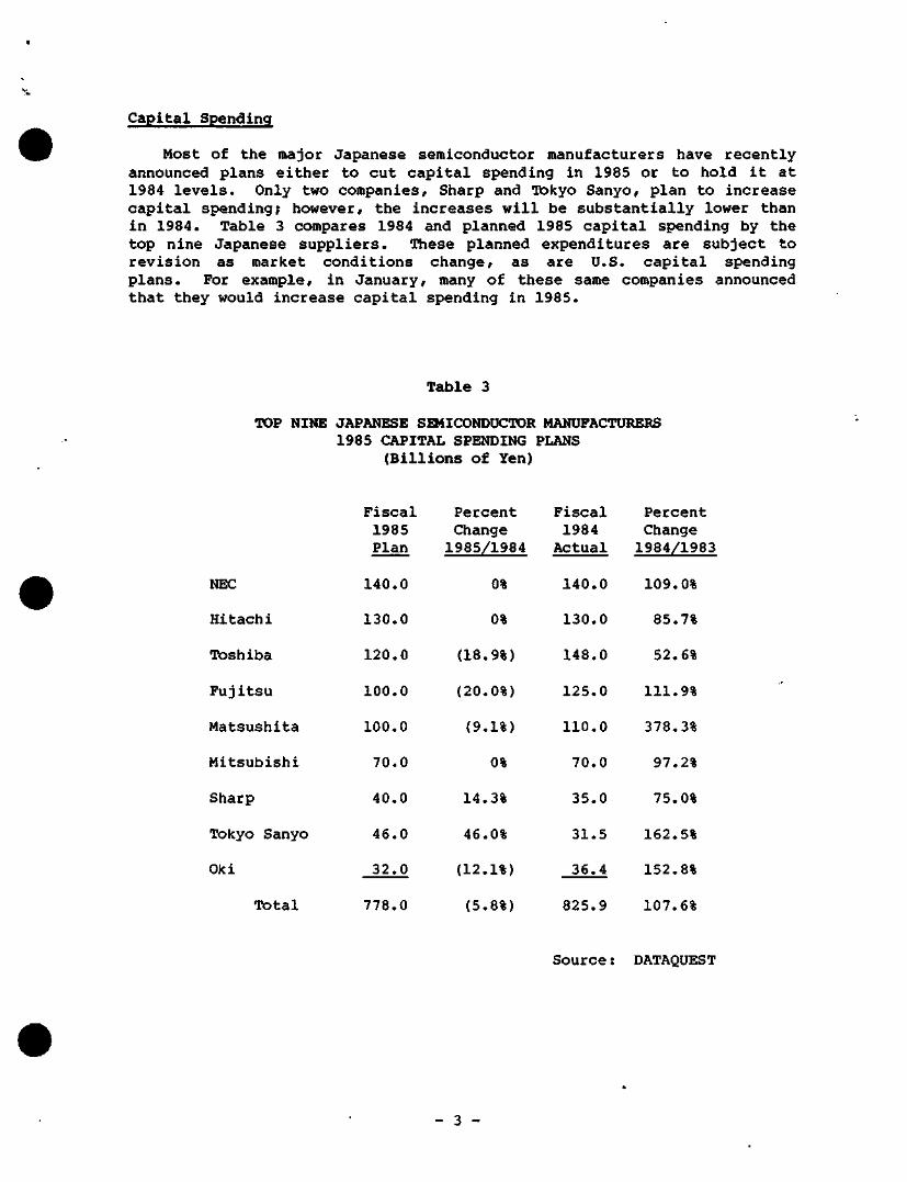
Capital Spending
Most of the major Japanese semiconductor manufacturers have recently announced plans either to cut capital spending in 1985 or to hold it at 1984 levels. Only two companies. Sharp and Tokyo Sanyo, plan to increase capital spending; however, the increases will be substantially lower than in 1984. Table 3 compares 1984 and planned 1985 capital spending by the top nine Japanese suppliers. These planned expenditures are subject to revision as market conditions change, as are U.S. capital spending plans. For example, in January, many of these same companies announced that they would increase capital spending in 1985.
Table 3
TOP NINE JAPANESE SEMICONDUCTOR MANUFACTURERS 1985 CAPITAL SPENDING PLANS
(Billions of Yen)
NEC
Hitachi
Toshiba
Fujitsu
Matsushita
Mitsubishi
Sharp
Tokyo Sanyo
Oki
Total
Fiscal 1985 Plan
140.0
130.0
120.0
100.0
100.0
70.0
40.0
46.0
32.0
778.0
Percent Change 1985/1984
0%
0%
(18.9%)
(20.0%)
(9.1%)
0%
14.3%
46.0%
(12.1%)
(5.8%)
Fiscal 1984 Actual
140.0
130.0
148.0
125.0
110.0
70.0
35.0
31.5
36.4
825.9
Percent Change 1984/1983
109.0%
85.7%
52.6%
111.9%
378.3%
97.2%
75.0%
162.5%
152.8%
107.6%
Source: DATAQUEST
- 3 -
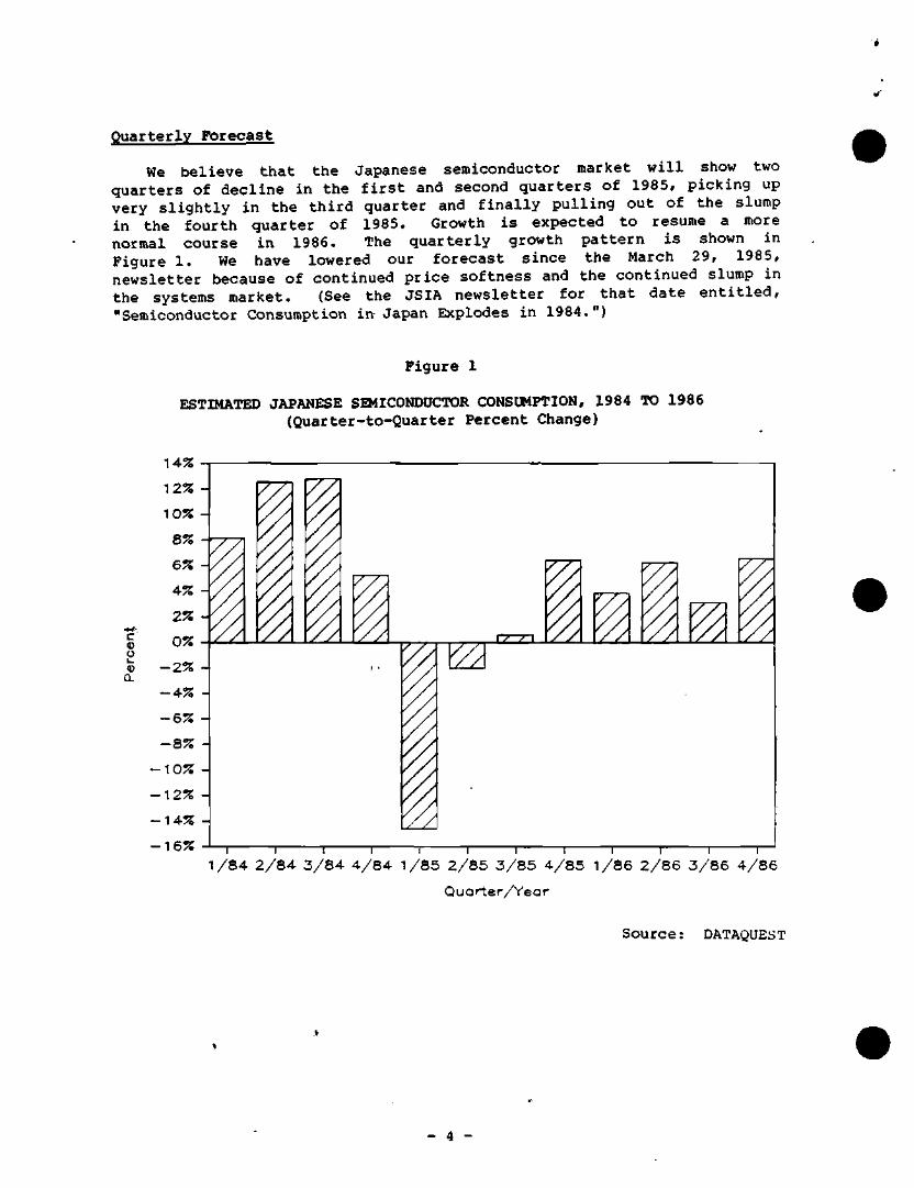
Quarterly Forecast
We believe that the Japanese semiconductor market will show two quarters of decline in the first and second quarters of 1985, picking up very slightly in the third quarter and finally pulling out of the slump in the fourth quarter of 1985. Growth is expected to resume a more normal course in 1986. The quarterly growth pattern is shown in Figure 1. We have lowered our forecast since the March 29, 1985, newsletter because of continued price softness and the continued slump in the systems market. (See the JSIA newsletter for that date entitled, "Semiconductor Consumption in- Japan Explodes in 1984.")
Figure 1
ESTIMATED JAPANESE SEMICONDUCTOR CONSUMPTION, 1984 TO 1986 (Quarter-to-Quarter Percent Change)
c o l_ V Q. m
rp-^^
T 1 ! 1 1 1 1 1 1 1 1 r 1 / 8 4 2 / 8 4 3 / 8 4 4 / 8 4 1 /85 2 / 8 5 3 / 8 5 4 / 8 5 l / S 6 2 / 8 6 3 / 8 6 4 / 8 6
Quarte r /Year
Sou rc e : DATAQUE S T
- 4 -
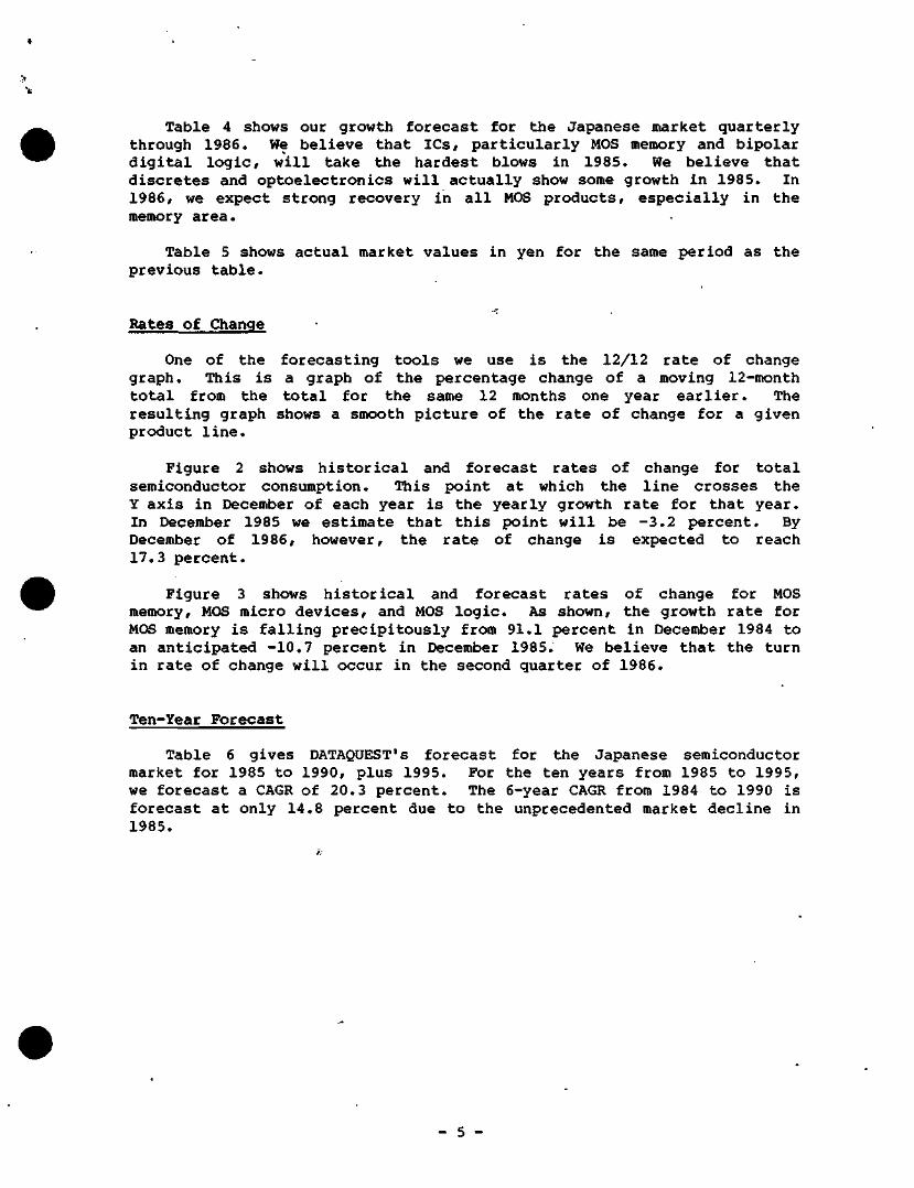
Table 4 shows our growth forecast for the Japanese market quarterly through 1986. We believe that ICs, particularly MOS memory and bipolar digital logic, will take the hardest blows in 1985. We believe that discretes and optoelectronics will actually show some growth in 1985. In 1986, we expect strong recovery in all MOS products, especially in the memory area.
Table 5 shows actual market values in yen for the same period as the previous table.
Rates of Change
One of the forecasting tools we use is the 12/12 rate of change graph. This is a graph of the percentage change of a moving 12-month total from the total for the same 12 months one year earlier. The resulting graph shows a smooth picture of the rate of change for a given product line.
Figure 2 shows historical and forecast rates of change for total semiconductor consumption. This point at which the line crosses the Y axis in December of each year is the yearly growth rate for that year. In December 1985 we estimate that this point will be -3.2 percent. By December of 1986, however, the rate of change is expected to reach 17.3 percent.
Figure 3 shows historical and forecast rates of change for MOS memory, MOS micro devices, and MOS logic. As shown, the growth rate for MOS memory is falling precipitously from 91.1 percent in December 1984 to an anticipated -10.7 percent in December 1985. We believe that the turn in rate of change will occur in the second quarter of 1986.
Ten-Year Forecast
Table 6 gives DATAQUEST's forecast for the Japanese semiconductor market for 1985 to 1990, plus 1995. For the ten years from 1985 to 1995, we forecast a CAGR of 20.3 percent. The 6-year CAGR from 1984 to 1990 is forecast at only 14.8 percent due to the unprecedented market decline in 1985.
- 5 -
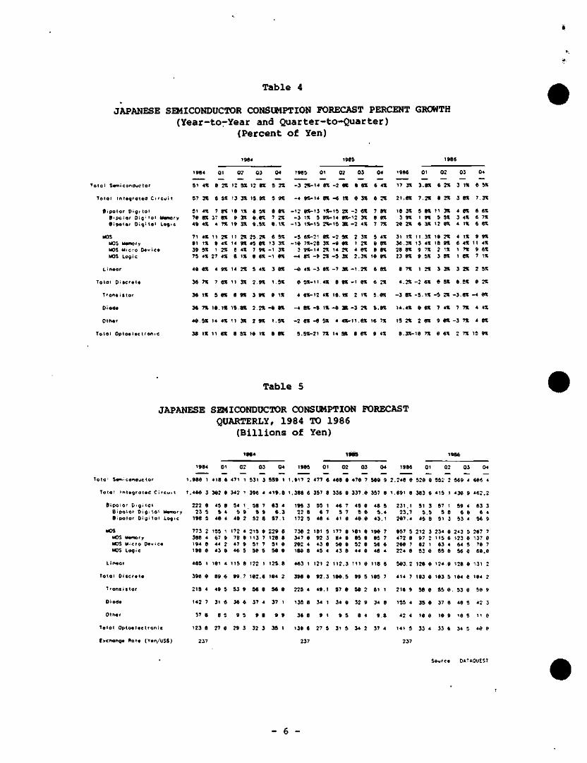
Table 4
JAPANESE SEMICONDUCTOR CONSUMPTION FORECAST PERCENT GROWTH ( Y e a r - t o - Y e a r and Q u a r t e r - t o - Q u a r t e r )
( P e r c e n t o f Yen)
1984 1985 1986
1984 01 02 03 04 1985 01 02 03 04 1986 01 0 2 03 04
T o t o l S«n lconauctor 51 4% 8 2% 12 5S 12 8S 5 23 - 3 2 ^ 1 4 6X - 2 R ( 6 6S 6 4X 17 3!( S .SX 6 2X 3 I X 6 5!!
T o t o l I n t ^ g r o t e a C . r e u i t 57 3« 8 5S 13 3S 15 .9S 5 9!! - 4 9S -14 8» - « 1« 6 JH 6 2S 2 1 , 8 X 7. 2S 8 2H 3 8» 7 . 3X
B i p o l o r O : g i t o ) 51 411 7 ffS 18 i n 8 511 8 9R - 1 2 6S-13 1%-15 3 - 3 6 X 7 8 1 t l B 3 X 5 8 » 1 1 3 » 4 e ! t 6 6X B i p c l a r O i g ' l o l Uamory 76 8X 37 8!l 9 3% » m T 7% - 3 IX 5 9S-14 9X-12 i% b m 3 9X 1 9X 5 SX 3 4X 6 71S B i p o l a r D i g i t o l Logic 49 4 » 4 7 » 19 3X 9 . 5 S 8 1» - 1 3 1» -15 2 S - 1 5 B - 2 4S 7 7% 26 2it 6 3X 12 « 4 1« 6 6S
MOS 71 4X 11 2X 11 2it 25.2R 6 5S - 5 6S-21 eJS - 2 S» 2 3S 5 4 1 31 IS 11 . 3S 16 2» 4 1« 9 9X UOS IMinory 91 IX 9 4Z 14 9X 45 8X 13 3X - 1 6 7X-2e 3X - 9 6X 1 2X 6 8X 3 6 . 3 X 13 4X 18 9X 6 4X 11 4X MOS Mic ro D « v i c t 39 5X 1 2X 8 4X 7 9X - 1 3X 3 95 -14 21t 14 2X 4 8X 8 8% 28 8X 9 7X 2 IX 1 7X 9 6X MOS Logic 75 4X 27 4X 8 IX 8 6X - 1 6X - 4 8S - 9 : X - 5 3X 2 . 3 X 16 eX 23 9X 9 5X 3 8X 1 8X 7 IX
L i ncor 46 6X 4 9X 14 2X 5 4X 3 6X - 6 4X - 3 6X - 7 3X -1 . 2X 6 8X 8 7X 1 2X 3 3X 3 2X 2 5X
T o t a l O i s c r . l . 3 6 . 7 X 7 6X 11 3X 2 . 9 X 1.5X 6 5 X - 1 1 - 4 X 8 9X - 1 eX 6 2X 4 .2X - 2 6X 6 5X e . 5 X 6 2%
I ' o n t i t t o r 36 IX 5 BX 8 9X 3 9X 6 1X 4 6X -12 4X 1«. IX 2 IX 5 . e X - 3 8X - 5 . IX - 5 2X - 3 . e x -4 eX
O i o d * 36 7X I B . I X 1S.8X 2 . 2 X - « SX - 4 8X - 8 I X - B SC - 3 2X 5 . 8 X 14 .4X 6 6X 7 4X 7 7X 4 4X
O t h * r 4B 5X 14 4X 11 3X 2 9X 1.SX - 2 «X - B 5X 4 « ( - t 1 6X 16 7X 15 2X 2 BX 9 BX - 3 7X 4 8X
T o t o l O p t o « l « c t r o n i c 38 IX 11 6X 8 5X 16 IX 8 8X 5 . 5 X - 2 1 7X 14 SX 8 6X 9 4X e . 3 X - i e 7X 6 6X 2 7X 15 9X
Table 5
JAPANESE SEMICONDUCTOR CONSUMPTION FORECAST QUARTERLY, 1984 TO 1986
( B i l l i o n s o f Yen)
1984 01 02 03 04 1985 01 02 03 04 1986 01 02 03 04
Totol S«"iiconaijctor 1.986 1 418.6 471 1 531 3 559 1 1.917 2 477 6 468 6 476 7 566 9 2.248 6 526 6 552 2 569 4 666 4
Toto! integrotta Circuit 1,466 3 362 6 342 1 396 4 419.8 1.388 6 357 8 336 6 337.6 357 8 1.691 8 383 6 415 1 436 9 462.2
Bipolor Digi tal 222 6 Bipolor Digital Memory 23 5 Bipolar Digital Logic 198 5 46
MCS MOS Memory MOS Micro Device I40S Logic
45 8 54 1 58 7 63 4 195 3 55 1 46 7 45 6 48 5 231.1 51 3 57 1 59 4 63 3 5 4 5 9 5 9 6.3 22 8 6 7 5 7 5 6 5 .4 23.7 5.5 5 8 6 6 6 4 46 4 48 2 52 8 57.1 172 5 48 4 41 6 46 6 43.1 2B7.4 45 8 51 3 53 4 56 9
773 2 155 1 172 4 215 9 229 8 736 2 181 5 177 6 181 6 196 7 957 5 212 3 234 e 243 5 267 7 388 4 67 9 78 B 113 7 128 8 347 6 92 3 84 6 85 6 85 7 472 8 97 2 115 6 123 6 137 6 194 e 44 2 47 9 51 7 51 6 262 4 43 8 56 6 52 6 56 6 266 7 62 l 63 4 64 5 76 7 196 6 43 B 46 5 56 5 56 6 186 8 45 4 43 B 44 6 48 4 224 B 53 6 55 6 56 6 66.6
Lineor 465 1 IBl 4 115 8 122 1 125 8 463 1 121 2 112.3 m B 118 6 563 2 126 6 124 6 128 6 131 2
Total Discrete 396 B 89 6 99 7 162.6 164 2 398 6 92 3 166.5 99 5 165 7 414 7 163 6 163 5 164 6 164 2
Tronsittor 215 4 49 5 53 9 56 6 56 B 225 4 49.1 57 B 58 2 61 1 216 9 58 6 55 6. 53 6 56 9
Diode 142 7 31 6 36 6 37 4 37 1 135 8 34 1 34 6 32 9 34 8 155 4 35 6 37 6 46 5 42 3
o t h e r 37 8 8 5 9 5 9 8 9 9 36 8 9 1 9 5 8 4 9 8 42 4 16 6 16 9 16 5 1 1 6
Totol Optoelectronic 123 8 27 8 29 3 32 3 35 1 136 6 27 5 31 5 34 2 37 4 141 5 33 4 33 6 34 5 46 6
E>cnonge Role (Ten/US») 237 237 237
Source DATAOUEST
- 6 -
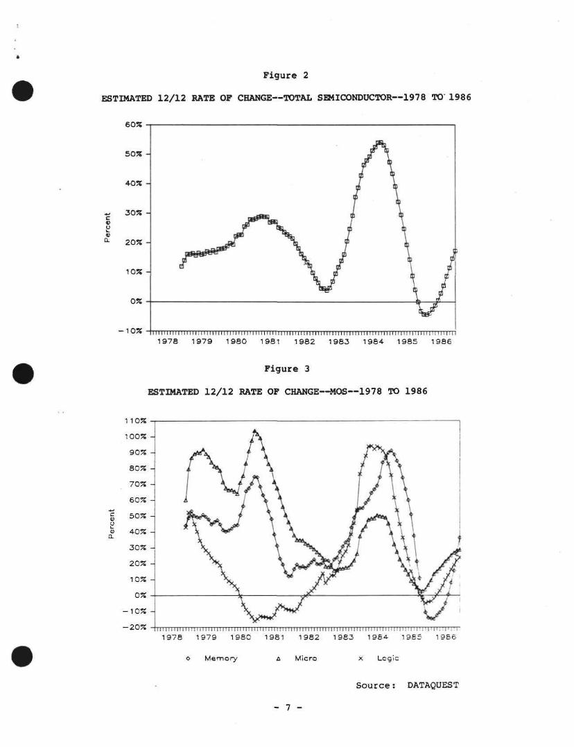
Figure 2
ESTIMATED 12/12 RATE OF CHANGE—TOTAL SEMICONDUCTOR—1978 TO 1986
60%
• • '0% niii i iIniTiiM'iiTriiM'inTiriT'nnTniiini'n'TiTTiii i i i i i i i i iMinii i i i i inTiTrrnmTi'nIt i i i i iI i ' ir iTiT'i i 1978 1979 1980 1981 1982 1983 1984 1985 1986
Figure 3
ESTIMATED 12/12 RATE OF CHANGE—MOS—1978 TO 1986
1 10%
c v o L.
(U CL
100% -
90% -
80% -
70% -
60% -
50% -
40% -
30% -
20% -
10% -
0 % -•
-10% -
•20% • t i i n i i i i i i i n i i i i i i i i i i i i ! i i i Imi i i i i i i i n i i TnnTmT iTn in i i nTnn i i i i i ( i u i i i i : i n i n iMWM! i ' i ' ! ; I ; 1978 1979 1980 1981 1982 1983 1984 19S5 1966
o Memory A Micro X Log!
S o u r c e : DATAQUEST
- 7 -
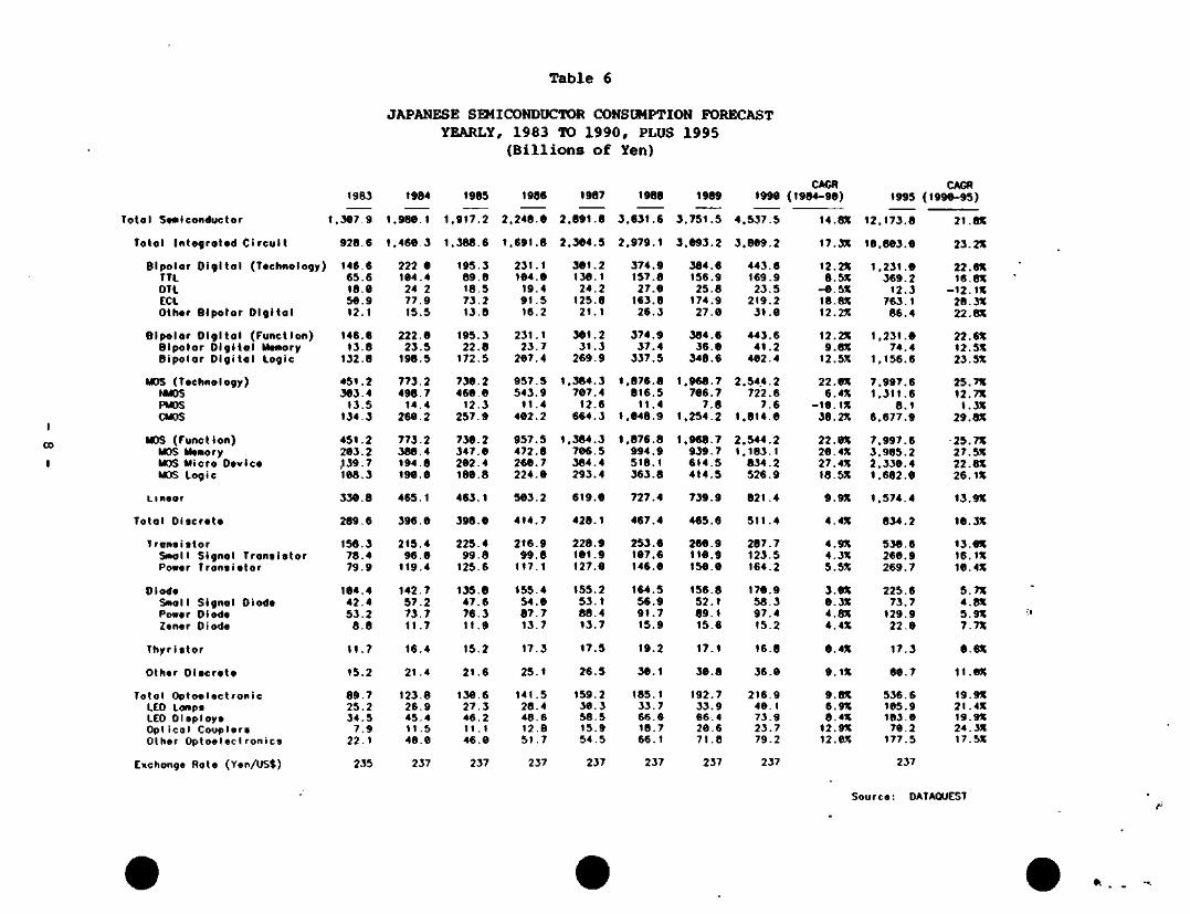
Tab le 6
JAPANESE SEMICONDUCTOR CONSUMPTION FORECAST YEARLY, 1983 TO 1 9 9 0 , PLUS 1995
( B i l l i o n s o f Yen)
I
00
Total Semiconductor 1
Totol In tegrotad C i r c u i I
Bipolar D i g i t a l (Technology) TTL DTL ECL Other Bipolar D i g i t a l
Bipolar D i g i t a l (Funct ion) Bipolar D i g i t a l Memory Bipolar D i g i t a l Logic
MOS (Technology) NMOS PMOS CMOS
MOS (Funct ion) MOS Memory MOS Micro Device MOS Logic
L inear
Total Discrete
Transistor Small Signal Transistor Power Transistor
Diode Small Signal Diode Power Diode Zener Diode
Thyristor
Other Discrete
Total Optoelectronic LED Lamps LED Displays Opt leal Couplers Other Optoelectronics
Exchonge Rote (Yen/US$)
19S3
307 9
928.6
146 .6 65 .6 18 .0 SO.9 12 .1
146 .6 13 .8
132 .8
451 .2 383 .4
13 .5 134 .3
451 .2 203 .2 ,139.7 108 .3
330 .8
289 .6
158 .3 78 . 4 79 .9
104.4 42 .4 53 .2
8 . 8
11 .7
15 .2
89 .7 25 .2 34 .5
7 .9 22 .1
1984
1.980 .1
1 .460 3
222 0 104.4 24 2 77 .9 15 .5
222 .0 23 .5
198 .5
773 .2 498 .7
14 .4 260 .2
773 .2 388 .4 194.8 190 .0
465 .1
396 .0
215 .4 9 6 . 0
119 .4
142 .7 57 .2 73 .7 11 .7
16 .4
21 . 4
123 .6 26.9 45 .4 11 .5 40.0
1985
1 .917 .2
1 .388 .6
195.3 8 9 . 8 18.5 73 .2 13 .8
195 .3 22 .8
172 .5
730 .2 460 .0
12 .3 257 .9
730 .2 347 .0 202 .4 180 .8
463 .1
398 .0
225 .4 99 .8
125.6
135.6 47 .6 76 .3 11 .9
15 .2
21 .6
130 .6 27 .3 46 .2 11.1 46 .0
1986
2 ,248 .0
1 . 6 9 1 . 8
231 .1 104.0
19 .4 91 .5 16.2
231 .1 23 .7
207 .4
957 .5 543 .9
11 .4 402 .2
957 .5 472 .8 260 .7 2 2 4 . 0
503 .2
414.7
216 .9 9 9 . 8
117 .1
155 .4 5 4 . 0 8 7 . 7 13.7
17 .3
25 .1
141 . 5 2 8 . 4 48 .6 12.8 51 . 7
1987
2 . 8 9 1 . 8
2 . 3 0 4 . 5
301 .2 130 .1 2 4 . 2
125 .8 21 .1
301 .2 31 .3
269 .9
1 .384 .3 707 .4
12 .6 6 6 4 . 3
1 . 3 8 4 . 3 706.5 384 .4 293 .4
619 .0
428 .1
228 .9 101 .9 127 .0
155 .2 53 .1 88 . 4 13 .7
17 .5
26 .5
159 .2 30 .3 58 .5 15 .9 54 ,5
1988
3 . 6 3 1 . 6
2 . 9 7 9 . 1
3 7 4 . 9 157 .8 27 .0
163 .8 26 .3
374 .9 37 . 4
337 .5
1 .876 .8 816 .5
11 .4 1 .048 .9
1 .876 .8 9 9 4 . 9 518.1 363 .8
727 .4
467 .4
253 .6 107 .6 146 .0
164.5 56 .9 9 1 . 7 15 .9
19 .2
30 .1
185 .1 33 .7 66 .6 18 .7 6 6 . 1
1989
3 . 7 5 1 . 5
3 . 0 9 3 . 2
384 .6 156 .9 25 .8
174.9 27 .0
384 .6 3 6 . 0
348 .6
1 .968 .7 706 .7
7 .8 1 .254 .2
1 .968 .7 939 .7 614 .5 414 .5
739 .9
465 .6
260 .9 110 .9 150 .0
156 .8 52 . 1 89 .1 15 .6
17 .1
3 0 . 8
192 .7 33 .9 66 . 4 20.6 7 1 . 8
1990
4 . 5 3 7 . 5
3 . 8 0 9 . 2
443.6 169 .9 23 .5
219 .2 3 1 . 0
443 .6 41 .2
402.4
2 .544 .2 722 .6
7 .6 1 . 8 1 4 . 0
2 . 5 4 4 . 2 1.183.1
8 3 4 . 2 526 .9
8 2 1 . 4
511 .4
287 .7 123 .5 164.2
170 .9 58 .3 97 . 4 15 .2
16 .8
36 .0
216.9 40 .1 73 .9 23 .7 79.2
CAGR (1984 -90)
14.8X
17.355
12.2X 8 .5X
- 0 . 5 X 18.8X 12 .2«
12.2X 9 .8X
12 .5n
22.OX 6 .4X
- 1 0 . I X 38 .2X
22.OX 20 .4X 27 .4X 18.5X
9 .9X
4 .4X
4.9X 4.3X 5 .5X
3.OX 0 .3X 4.8X 4.4X
e . 4X
9 . I X
9 .8X 6 .9X S .4X
12.9X 12.0X
12
10
1
1
1
7 1
6
7 3 2 1
1
1995
. 1 7 3 . 8
,803 .0
. 2 3 1 . 0 369 .2
12 .3 763.1
86 . 4
. 2 3 1 . 0 74 .4
. 156 .6
,997 .6 . 3 1 1 . 6
8 . 1 . 6 7 7 . 9
. 9 9 7 . 6
. 9 8 5 . 2
. 3 3 0 . 4
. 6 8 2 . 0
. 574 .4
834 .2
530 .6 260 .9 269 .7
225 .6 73 .7
129 .9 22 .0
17 .3
60 .7
536 .6 105 .9 183.0 70.2
177 .5
CAGR (1990-95)
21.8X
23 .2X
22 .6X 16.8X
- 1 2 . I X 28 .3X 22 .8X
22 .6X 12.5X 23 .5X
25 .7X 12.7X
1.3X 29 .8X
25 .7X 27 .5X 22 .8X 26 . IX
13.9X
10.3X
13.OX 1 6 . I X 10 .4X
5 .7X 4.8X 5 .9X 7 .7X
e .6X
11.OX
19.9X 2 1 . 4X 19.9X 24. 3X 17.5X
235 237 237 237 237 237 237 237 237
Source: OATAQUEST
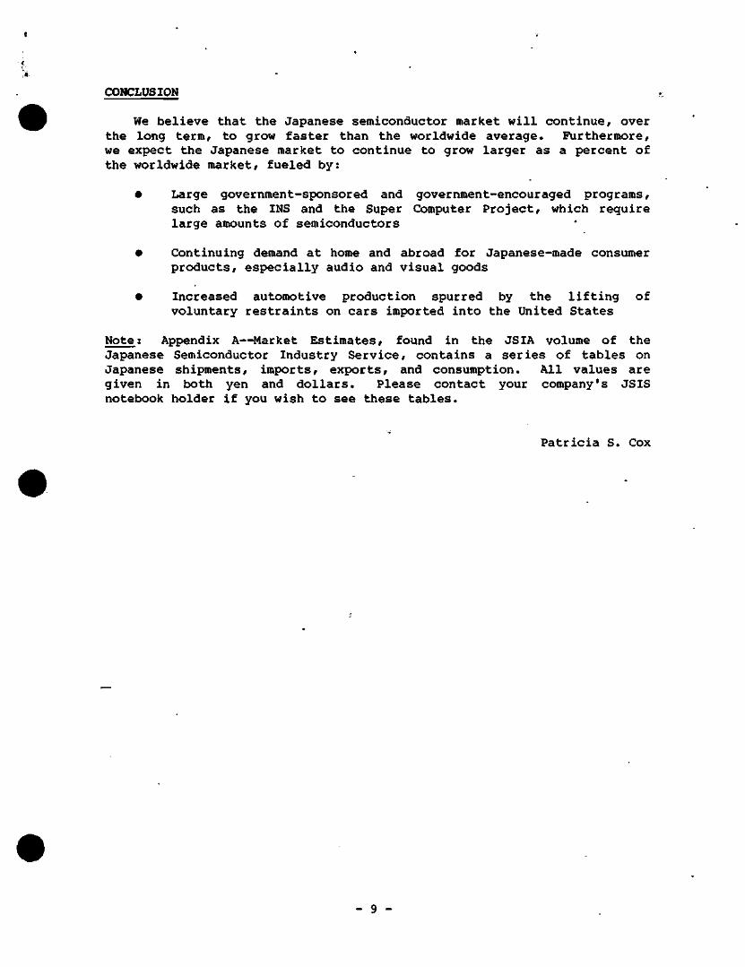
t
CONCLUSION
We believe that the Japanese semiconductor market will continue, over the long term, to grow faster than the worldwide average. Furthermore, we expect the Japanese market to continue to grow larger as a percent of the worldwide market, fueled by:
• Large government-sponsored and government-encouraged programs, such as the INS and the Super Computer Project, which require large amounts of semiconductors
• Continuing demand at home and abroad for Japanese-made consumer products, especially audio and visual goods
• Increased automotive production spurred by the lifting of voluntary restraints on cars imported into the United States
Note; Appendix A—^Market Estimates, found in the JSIA volume of the Japanese Semiconductor Industry Service, contains a series of tables on Japanese shipments, imports, exports, and consumption. All values are given in both yen and dollars. Please contact your company's JSIS notebook holder if you wish to see these tables.
Patricia S. Cox
- 9 -
JSIA Code: Newsletters
THE SIMICONDUCTOR START-UP BOOM CONTINUES
Despite the industry downturn, semiconductor start-ups are alive and well. As shown in Table 1, DATAQUEST's Japanese Semiconductor Industry Service has recorded 47 semiconductor start-ups since late 1983—a record for the industry. This figure tops the 29 start-up companies recorded for the same period covered by our last newsletter on this subject, "Asian Ties with U.S. Semiconductor Start-Ups," January 18, 1984. Twenty-eight of the start-ups are located in Silicon Valley. DATAQUEST believes that there are at least 10 more start-up companies that have not yet been publicly announced. We believe that the continuing boom in semiconductor start-ups reflects the emergence of new market niches in application-specific ICs (ASICs), CMOS memory and logic, gallium arsenide (GaAs), linear, digital signal processing (DSP), and silicon compilers.
A major development is the growing number of ties between Asian electronics companies and U.S. semiconductor start-ups. Some of the more notable alliances are as follows:
• Barvon Research—Licensing agreement with Ricoh
• China Micro—British-Chinese joint venture
• Ixys Corporation—Ricoh wafers
• Modular Semiconductor—Licensing of CMOS 256K DRAM and 16K SRAM to Ricoh
• Mosel—First round Taiwan investors
NMB Semiconductor—Subsidiary of Minebea Co. (Tokyo ball bearing maker)
Panatech Semiconductor—Sales and Marketing agreement with Ricoh
Quasel—Joint venture with Taiwanese investors
SID Microelectronica S.A.—Sales of Sharp products
C 1985 Dataquest Incorporated May 16 ed.-Reproduction Prohibited
Tne conteni o( tnis
p i o . . a e a t o u s i n r ,
reoor
nlUlRF
Of an
reoresonl
, . e l i , o> . . r
o l l eMo B.
s ou
l e n
nlerDretalion an
s Individual co" i
c j f i t i es Tnis (irrr
d anaty
. ,n i , . . , ,
ana Its
SISOl
, | ,o, le,
pdien!
lorn
a n a
nal iong
naanai
• " " " " '
nneral
IBdb
o l ' i ce ,
y a . a d a b l P I o ,
DATAQLiEST
s Mocknaider
h e
m a
0 ,
b e
m e n
C d .
l i e
b e
re
IS
easec
0' in
i b e
b y
S , l
''
respor
d l.r 0
n i ies
sible individuals i
nef DATAQUEST s
n a , l . o m . i m e . o ,
( b e
e.vice
me n
ubiecl cdmpanie
s Tb is in lo ima!
a v e a i o n g o r s b d
s bu
n i s
i p b
i i s n o l g u a r a i
ml (uin ..bed
i b o n i n i b e s e
Bed as
:anm.
.unl ies
o a r
m e n
cura
* i l
-one
y d i c d
a .sale
, and m
npieleness
i d d e i l b s e
a , sell 0. bu
" . . . , tTwun<i " i i 'n rT i . i ^ r i« i
s e c u n b e s b r m c a n n e c b o ,
sucn securibes
Dataquest Incorporated, A Subsidiary of A.C. Nielsen Company / 1290 Ridder Park Drive / San Jose, CA 95131 / (408) 971-9000 / Telex 171973
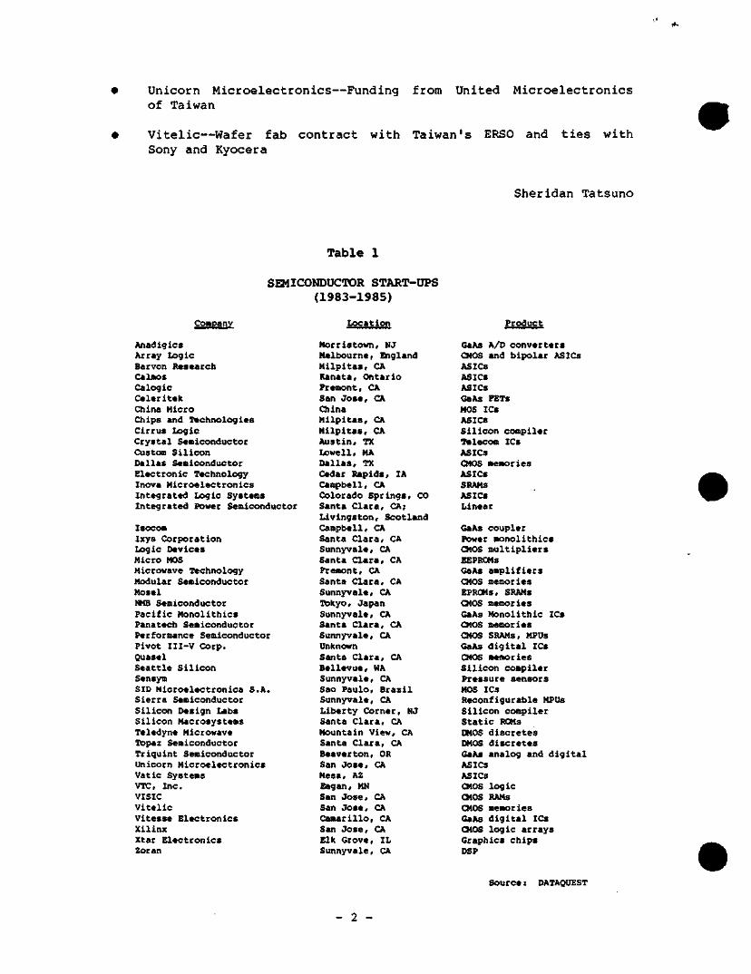
• Unicorn Microelectronics—Funding from United Microelectronics of Taiwan
• Vitelic—Wafer fab contract with Taiwan's ERSO and ties with Sony and Kyocera
Sheridan Tatsuno
Table 1
SEMICONDUCTOR START-UPS (1983-1985)
Company
Anadigics Array Logic Barvon Research Calnos Caloglc Celeritek China Micro Chips and Technologies cirrus Logic Crystal Semiconductor Custom Silicon Dallas Semiconductor Electronic Technology Inova Microelectronics Integrated Logic Systems Integrated Power Semiconductor
Isocom Ixys Corporation Logic Devices Micro MOS Microwave Technology Modular Semiconductor Mosel NMB Semiconductor Pacific Honolithlcs Panatech Semiconductor Performance Semiconductor Pivot III-V Corp. Quasel Seattle Silicon Sensym SID Mlcroelectronica S.A. Sierra Semiconductor Silicon Design Labs Silicon Macrosystems Teledyne Microwave Topaz Semiconductor Triquint Semiconductor Unicorn Microelectronics Vatic Systems VTC, Inc. VISIC Vitelic Vitesse Electronics Xillnx Xtar Electronics Zoran
Location
Horristown, NJ Melbourne, England Milpltas, CA Kanata, Ontario Fremont, CA San Jose, CA China Milpltas, CA Milpltas, CA Austin, TX Lowell, HA Dallas, TX Cedar Kapids, lA Campbell, CA Colorado Springs, CO Santa Clara, CA; Livingston, Scotland Campbell, CA Santa Clara, CA Sunnyvale, CA Santa Clara, CA Fremont, CA Santa Clara, CA Sunnyvale, CA ToI<yo, Japan Sunnyvale, CA Santa Clara, CA Sunnyvale, CA Unknown Santa Clara, CA Bellevue, WA Sunnyvale, CA Sao Paulo, Brazil Sunnyvale, CA Liberty Corner, NJ Santa Clara, CA Mountain View, CA Santa Clara, CA Beaverton, OR San Jose, CA Mesa, AZ Eagan, MN San Jose, CA San Jose, CA Caroarlllo, CA San Jose, CA Elk Grove, IL Sunnyvale, CA
Product
GaAs A/D converters CMOS and bipolar ASICs ASICs ASICs ASICs GaAs FETS MOS ICs ASICs Silicon compiler Telecom ICs ASICs CMOS memories ASICs SRAMS ASICs Linear
GaAs coupler Power monolithics CMOS multipliers EEPROMS GaAs amplifiers CMOS memories EPRCMs, SRAMS QIOS memories GaAs Monolithic ICs OlOS memories CMOS SRAMS, MPUs GaAs digital ICs CMOS isemorles Silicon compiler Pressure sensors HOS ICs Reconfigurable MPUs Silicon compiler Static ROMs DMOS discretes OMOS discretes GaAs analog and digital ASICs ASICs OlOS logic CMOS RAMs CMOS memories GaAs digital ICs QIOS logic arrays Graphics chips DSP
Sou rce: DATAQtJEST
- 2 -
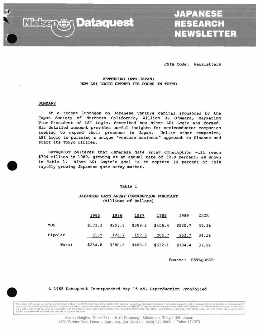
Dataquest JAPANESE RESEARCH NEWSLETTER
JSIA Code: Newsletters
VENTURING INTO JAPAN: HOW LSI LOGIC OPENED ITS DOORS IN TOKYO
SUMMARY
At a recent luncheon on Japanese venture capital sponsored by the Japan Society of Northern California, William J. O'Meara, Marketing Vice President of LSI Logic, described how Nihon LSI Logic was formed. His detailed account provides useful insights for semiconductor companies seeking to expand their presence in Japan. Unlike other companies, LSI Logic is pursuing a unique "venture business" approach to finance and staff its Tokyo offices.
DATAQtJEST believes that Japanese gate array consumption will reach $794 million in 1989, growing at an annual rate of 32.9 percent, as shown in Table 1. Nihon LSI Logic's goal is to capture 10 percent of this rapidly growing Japanese gate array market.
Table 1
JAPANESE GATE ARRAY CONSUMPTION FORECAST (Millions of Dollars)
1985 1986 1987 1988 1989 CAGR
MOS
Bipolar
Total
$173.3
81.5
$254.8
$253.8
126.7
$380.6
$309.2
157.0
$466.2
$406.4
205.7
$612.1
$530.7
263.7
$794.4
32.3%
34.1%
32.9%
Source: DATAQUEST
© 1985 Dataquest Incorporated May 15 ed.-Reproduction Prohibited
The content of this report represents our interpretaion and analysis of information generally available to the public or released by responsible individuals in the subject companies, but is not guaranteed as to accuracy or completeness It does not contain matericil provided to us in confidence by our clients Individual companies reported on and analyzed by DATAQUEST, may be clients of this and/or other DATAQUEST services This information is not furnished in connection with a sale or offer to sell securities or in connection with the solicitation ol an offer to buy securities This firm and its parent and/or their officers, stockholders, or members of their families may, from time to time, have a long or short position in the securities mentioned and may sell or buy such securities
Azabu Heights, Suite 711, 1-5-10 Roppongi, Minato-ku, Tokyo 106, Japan 1290 Ridder Park Drive / San Jose, CA 95131 / (408) 971-9000 / Telex 171973
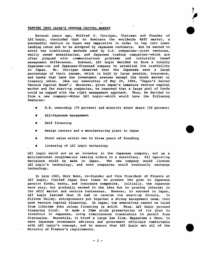
TAPPING INTO JAPAN'S VENTURE CAPITAL MARKET
Several years ago, Wilfred J. Corrigan, Chairman and Founder of LSI Logic, concluded that to dominate the worldwide ASIC market, a successful venture in Japan was imperative in order to tap into lower lending rates and to be accepted by Japanese customers. But he wanted to avoid the traditional methods used by U.S. companies—joint ventures, wholly owned subsidiaries, and Japanese trading companies—which are often plagued with communications problems and culturally based management differences. Instead, LSI Logic decided to form a totally Japanese-run and Japanese-financed company to establish its credibility in Japan. Mr. Corrigan observed that the Japanese save a large percentage of their income, which is held by large pension, insurance, and banks that have few investment avenues except the stock market or treasury notes. (See our newsletter of May 29, 1984, "Japan's Second Venture Capital Boom".) Moreover, given Japan's immature venture capital market and few start-up companies, he reasoned that a large pool of funds could be tapped with the right management approach. Thus, he decided to form a new company—Nihon LSI Logic—which would have the following features:
U.S. ownership (70 percent) and minority stock share (30 percent)
All-Japanese management
Self financing
Design centers and a manufacturing plant in Japan
Stock sales within two to three years of founding
Licensing of LSI Logic technology
LSI Logic would act as an investor in the Japanese company, not as a multinational conglomerate issuing orders to a subsidiary. All operating decisions would be made in Japan. The new company would license LSI Logic's technology, and both companies would eventually exchange technology.
In late 1983, Mick Bohn, co-founder and Vice President of Finance at LSI Logic, visited Japan four times to present the plan to Japanese pension funds, banks, and insurance companies. Initially, the Japanese were wary, but gradually warmed to the idea due to growing interest in the ASIC market and venture businesses. However, to succeed in Japan, LSI Logic learned that it had to reverse its start-up formula. In Silicon Valley, entrepreneurs put together a strong management team, then seek venture capital financing. In Japan, top executives cannot be lured from lifetime jobs unless financing is solid. Thus, LSI Logic pursued financing first. It made a 35mm slide presentation of its plan to investors in Japanese, using simultaneous translators to permit free discussion. Meanwhile, it hired a large law firm, Nagashima & Ohno, to make Japanese investment advisors and government officials comfortable with LSI Logic's concept, and to ensure that LSI Logic met all of the Ministry of Finance's requirements.
- 2 -
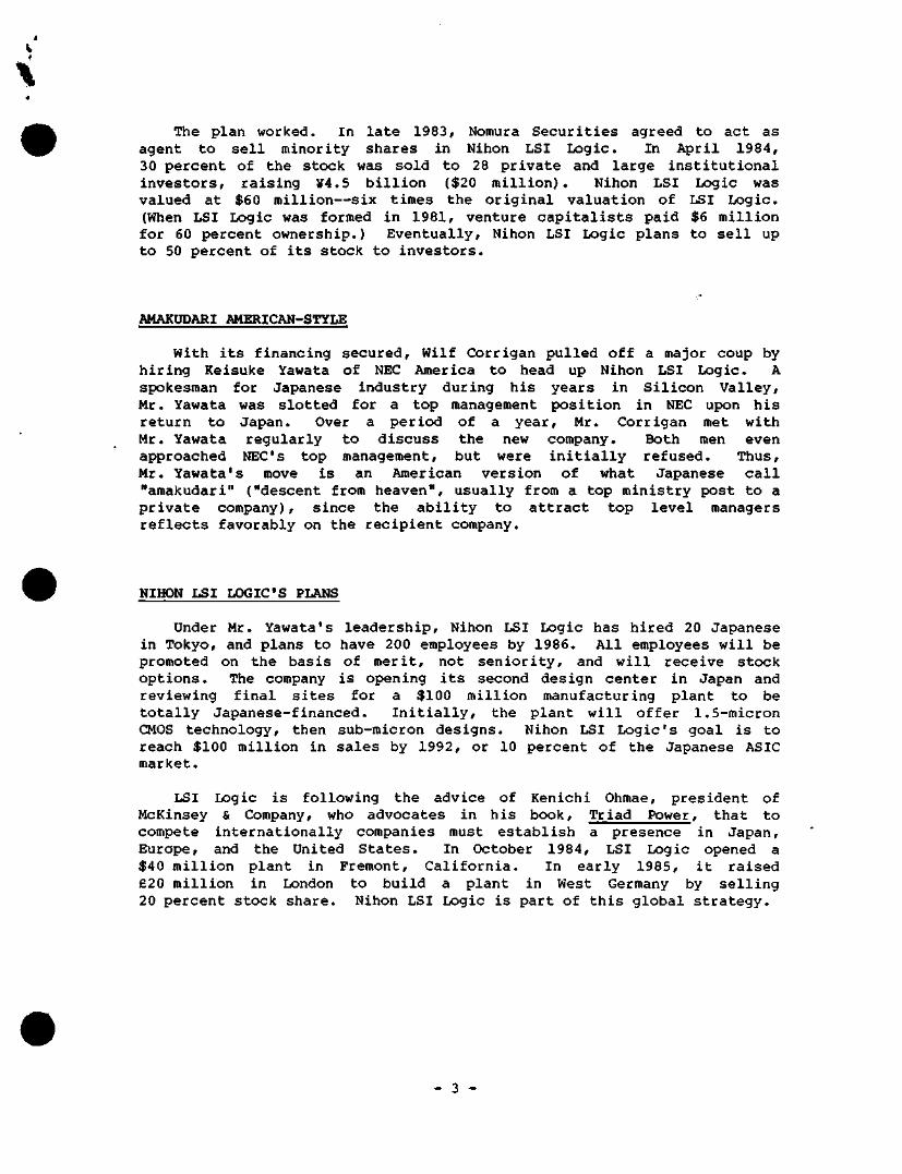
The plan worked. In late 1983, Nomura Securities agreed to act as agent to sell minority shares in Nihon LSI Logic. In April 1984, 30 percent of the stock was sold to 28 private and large institutional investors, raising ¥4.5 billion ($20 million). Nihon LSI Logic was valued at $60 million—six times the original valuation of LSI Logic. (When LSI Logic was formed in 1981, venture capitalists paid $6 million for 60 percent ownership.) Eventually, Nihon LSI Logic plans to sell up to 50 percent of its stock to investors.
AMAKPDARI AMERICAN-STYLE
With its financing secured, Wilf Corrigan pulled off a major coup by hiring Keisuke Yawata of NEC America to head up Nihon LSI Logic. A spokesman for Japanese industry during his years in Silicon Valley, Mr. Yawata was slotted for a top management position in NEC upon his return to Japan. Over a period of a year, Mr. Corrigan met with Mr. Yawata regularly to discuss the new company. Both men even approached NEC's top management, but were initially refused. Thus, Mr. Yawata's move is an American version of what Japanese call "amakudari" ("descent from heaven", usually from a top ministry post to a private company), since the ability to attract top level managers reflects favorably on the recipient company.
NIHON LSI LOGIC'S PLANS
Under Mr. Yawata's leadership, Nihon LSI Logic has hired 20 Japanese in Tokyo, and plans to have 200 employees by 1986. All employees will be promoted on the basis of merit, not seniority, and will receive stock options. The company is opening its second design center in Japan and reviewing final sites for a $100 million manufacturing plant to be totally Japanese-financed. Initially, the plant will offer 1.5-micron CMOS technology, then sub-micron designs. Nihon LSI Logic's goal is to reach $100 million in sales by 1992, or 10 percent of the Japanese ASIC market.
LSI Logic is following the advice of Kenichi Ohmae, president of McKinsey & Company, who advocates in his book. Triad Power, that to compete internationally companies must establish a presence in Japan, Europe, and the United States. In October 1984, LSI Logic opened a $40 million plant in Fremont, California. In early 1985, it raised £20 million in London to build a plant in West Germany by selling 20 percent stock share. Nihon LSI Logic is part of this global strategy.
- 3 -
ENTERING THE JAPANESE MARKET
DATAQUEST believes that the only way to compete internationally with Japanese semiconductor companies is to establish a major presence in Japan. Companies such as Fairchild, Motorola, and Texas Instruments have successfully penetrated the bipolar market because of their local manufacturing capabilities. Recently, AMI, Nihon LSI Logic, and Thomson CSF have opened local design centers in Japan to enter the highly competitive ASIC market.
To finance and staff these operations, we believe that several routes are available to non-Japanese companies:
• Local financing:
Japan Development Bank (JOB) loans—7.3 percent for research centers and plant facilities in any of the 15 Technopolis zones (such as Materials Research Corporation's Gita plant)
Regional bank financing—Secured with the assistance of local prefecture industry and government leaders
Venture capital financing (Nihon LSI Logic)
Local government tax incentives and special land writeoffs (Fairchild's Nagasaki plant, Monsanto*s Utsunomiya plant)
- Joint ventures with cash-rich conglomerates seeking new markets (AMI and Asahi Chemical)
• Staffing:
Hire internationally minded Japanese executives with overseas experience (Nihon LSI Logic's Mr. Yawata, Motorola's Dr. Iriye, DATAQUEST's Mr. Morishita)
Hire mid-level managers and professionals (IBM, DATAQUEST)
- Establish joint technology development with a Japanese company (Thomson CSF and Oki)
Sheridan Tatsuno
- 4 -
Dataquest JAPANESE . RESEARCH NEWSLETTER
JSIA Code: Newsletters
DATAQUEST'S JAPANESE CONFERENCE DEBUT— FAR EAST INDUSTRY: ACHIEVEMENTS AND CHALLENGES
SUMMARY
DATAQUEST's Japanese Semiconductor Industry Service (JSIS) held its first annual conference April 14-16 at the Hakone Prince Hotel, Hakone, Japan (south of Tokyo). The conference was completely sold out. The 210 attendees heard 21 industry leaders, government officials, and DATAQUEST analysts speak at this first-ever, full-length DATAQUEST Japanese conference. Speakers and attendees represented U.S., European, Japanese, Korean, and Taiwanese companies and government agencies. It is particularly noteworthy that more than half of the attendees were Japanese, and about the same percentage were top-level executives. Keynote speakers were Dr. Atsuyoshi Ouchi, Vice Chairman of NEC Corporation, and Mr. W. J. Sanders III, Chairman, President, and CEO of Advanced Micro Devices, Inc.
The conference theme, "Far East Industry: Achievements and Challenges," was particularly timely because of the great achievements made by the Japanese semiconductor industry in the last five years, the emergence of Taiwan and Korea as fast-growing participants in the semiconductor industry, and the highly publicized challenge being posed to U.S. and European suppliers in their attempts to penetrate Japanese industry.
This newsletter will cover the major topics addressed at the conference in the areas of market trends and strategies, trade and technology issues, equipment and materials, and product trends. Conference notebooks were distributed to all conference attendees and will be mailed to subscribers who did not attend the conference. Readers who wish to read specific speeches should contact their companies' JSIS notebook holder or conference attendee.
© 1985 Dataquest Incorporated May 8 ed.-Reproduction Prohibited
The content of this report represents our interpretaion and analysis of information generally available lo the public or reIeased by responsible individuals in the subject companies, but is not guaranteed as to accuracy or completeness It does not contain material provided to us in confidence by our clients Individual companies reported on and analyzed by DATAQUEST, may be clients of this and/or other DATAQUEST services This information is not furnished in connection with a sale or offer to sell securities or in connection with the solicitation of an offer to buy securities. This firm and its parent and/or their officers, stockholders, or members of their families may. from time to time, have a long or short position in the securities mentioned and may sell or buy such securities
Azabu Heights, Suite 711, 1-5-10 Roppongi, Minato-ku, Tokyo 106, Japan 1290 Ridder Park Drive / San Jose, CA 95131 / (408) 971-9000 / Telex 171973
i MARKET TRENDS AND STRATEGIES
Overview
DATAQUEST's Fred Zieber, Senior Vice President and Semiconductor Division Manager, kicked off the conference with an updated world semiconductor outlook. Predicting that the worldwide semiconductor market will grow only 2 percent in 1985, he blamed the disastrous first quarter of 1985 on a confluence of tremendous change in expectations, overbookings, a weak PC market, and very high prices in early- and mid-1984, which fell like a rock. He cited a growing U.S. economy and growth in real semiconductor usage as reasons for continued long-term growth of the industry. Mr. Zieber also pointed out the increasing ratio of materials cost to manufacturing, and projected a steadily decreasing trend for return on capital invested.
Sheridan Tatsuno, JSIS Research Analyst and author of an upcoming book entitled "Technology: Japan's HiTech Strategy for the 21st Century," noted a high correlation between the growth of Japanese-based companies' share of the world IC market, the Japanese share of the U.S. IC market, and the steadily increasing Japanese companies' share of papers presented at the International Solid State Circuits Conference. This correlation suggests that Japan is moving ahead quickly in both sales and technological expertise. He pointed to the dramatic increase in joint ventures and licensing between Japanese and Other firms as signaling a change from the "we vs. them" philosophy to a new philosophy of sharing and working together. Mr. Tatsuno presented DATAQUEST's forecast of 7 percent growth for the Japanese market in 1985, with a caution that this figure is at the upper end of our current range of 0 to 7 percent.
Japanese Viewpoint
Tomihiro Matsumura, Senior Vice President of NEC, spoke on "Japanese Semiconductor Industry—The Coming New Age." (Mr. Matsumura received a special award from Japan's Ministry of Science and Technology on the day he spoke at the DATAQUEST Conference, for his work in developing NEC's V-Series of originally developed microprocessors.
He noted that only two Japanese semiconductor companies were in the top ten worldwide in 1975, while in 1984, five were in the top ten. He believes that this is due to:
• Creating new markets (i.e., not just waiting for the economy to turn up)
• Emphasizing mass production rather than R&D
• Having available a much larger pool of engineering graduates to draw from than either the United States or Europe
- 2 -
Regarding export sales, Mr. Matsumura suggested that to ease trade friction, 50 percent of overseas sales should be produced in the country in which they will be sold.
Tsuyoshi Kawanishi, Director and Group Executive of Toshiba, spoke on the topic "Concentrated or Well-Balanced Products Strategy?" He believes that in general, U.S. semiconductor companies tend to concentrate on specific products, while Japanese companies tend to have more balanced product lines including heavy emphasis on discrete devices. While the concentrated strategy offers capital investment concentration, clear strategy, a strong corporate image in the areas of concentration, and phases of extremely high growth, it also leads to decreased stability during downturns and an inability to provide customers with a full line of products. On the other hand, the well-balanced strategy offers technology growth due to interrelationships of products, stability, and ability to service all the customers' needs. Drawbacks include a weak corporate image, unclear strategy, and inability to concentrate capital investment.
Korea and Taiwan
Irving T. Ho, President of Taiwan's Institute of Information Industry and the holder of 36 patents in computer hardware and subsystems, spoke on "The Recent Development of the Information Industry in Taiwan." In 1979, Taiwan instituted a strategic policy of developing a domestic information industry. The results of this policy are dramatic. In 1983, for the first time, Taiwan's electrical and electronic exports exceeded textile exports. Information product exports, especially computers, have experienced the highest growth of any electronics products. Dr. Ho provided information on the major electronics producers and exporters in Taiwan, and discussed major products and companies. He revealed the heavy investment plans of IC producers in Taiwan over the next three to five years. All IC manufacturers in Taiwan cooperate extensively with ERSO, the semi-governmental IC technology company. ERSO now has 2-micron Si-gate CMOS technology with single poly and double metal.
P. June Min, Senior Managing Director of Goldstar Semiconductor, Ltd., spoke on "The Emerging Korean Semiconductor Industry." Dr. Min presented many tables detailing semiconductor production and consumption in Korea, for which he sees very high growth in the next several years. The Korean electronics industry began with Korean companies manufacturing for Others on an OEM basis. Today, Korean name brand goods are sold worldwide. As in Japan, Korean semiconductor companies are parts of large, vertically integrated organizations. Also similarly to the Japanese, Korean companies are obtaining much of their design technology through licensing agreements with U.S. and European firms, although their processing technology is domestically developed. Dr. Min expects Korean semiconductor sales to triple by 1988.
- 3 -
A U.S. Look at Japan
Eugene J. Flath, Vice President and Assistant General Manager of Intel International, spoke on "A Fresh Look at Japan and Asia," a topic for which he is well qualified, having recently moved to Japan and become responsible for expanding Intel's presence in Japan and the Pacific Basin. Mr. Flath outlined the history of the U.S. semiconductor industry, which began with vertically integrated companies and now consists of many small- to mid-size companies specializing in semiconductors. This current state contrasts with the Japanese industry, which is dominated by vertically integrated manufacturers. He believes that due to the continually escalating cost of materials, most new capacity expansion will be in the Pacific Basin. He also believes that in order to support the Japanese market in a major way, foreign companies must build manufacturing facilities in Japan. This represents a radical change of view on Intel's part.
TRADE AND TECHNOLOGY
The areas of international trade and cooperation and government policy were very timely, since the conference was held during the height of tension in the trade negotiations between the United States and Japan.
Keynote Speakers
The conference keynote speakers, Atsuyoshi Ouchi of NEC and W. J. Sanders III of AMD, both spoke on these issues at dinner.
Dr. Ouchi struck a conciliatory tone regarding international trade relations. He believes that if the captive portion of the U.S. semiconductor market is accounted for, then Japanese companies actually have a smaller portion of the U.S. semiconductor market than the U.S. companies have of the Japanese semiconductor market. He also reminded Mr. Sanders that NEC is a major purchaser of AMD's ICs. Dr. Ouchi compared the completely open semiconductor market, which he thinks should exist, with contract bridge. He said that in a properly operating market, as in contract bridge, partners give each other signals that can be seen and understood by all partners, and all players follow the same rules. The perception now is that too much of the game is being played behind closed doors.
Mr. Sanders spoke pointedly on the U.S.-Japan trade imbalance and the difficult barriers U.S. companies face in the Japanese marketplace. While supporting the need for free international trade as vital to the free world's economic security, he termed the current imbalance "intolerable," and called for the United States to act unilaterally to provide incentive—in the form of U.S. trade barriers—to promote more openness in Japanese markets. Mr. Sanders supported his statement that barriers do exist in the Japanese semiconductor market by demonstrating that U.S. firms outperform their Japanese counterparts in the neutral markets of Europe and Rest of World. He called for "affirmative action" on the part of Japanese companies and consumers to buy more U.S. goods.
- 4 -
Government View
Clyde Prestowitz, Counselor on Japan to the U.S. Secretary of Commerce, spoke on "Government Involvement: Help or Hindrance." He noted that the U.S. government has both helped and hindered the U.S. semiconductor industry. While aiding the industry through military procurement, the Department of Defense (DoD) also hinders its ability to exploit overseas markets because the DoD makes it difficult to obtain the necessary export licenses. On the other hand, the Japanese government's efforts have been more focused and more continuous in aiding the Japanese semiconductor industry. He believes that in the matter of trade, there has been a lot of talk but little communication. He also cited several examples of instances in which, because of the bureaucratic Japanese system, U.S. companies were discriminated against, even though discrimination may not have been intended. Mr. Prestowitz noted that the Japanese still view themselves as a very small, developing country. He has been told, during the course of his trade negotiations, that "little baby companies" such as NEC and Hitachi cannot compete with "great sumo wrestler companies" like IBM and AT&T on a global basis.
Presenting the Japanese government's perspective was Shoichi Ito, a technical official from the Ministry of International Trade and Industry (MITI) . Mr. Ito stood in for Hiroshi Shima, who was called at the last minute to testify in the Diet on the proposed Japanese chip protection act. Mr. Ito's topic was, "Status Quo and Tomorrow, Japanese Semiconductor Industry." He stated MITI's position that Japan and the United States "should strive for even freer semiconductor trade, and work to avoid regulative actions while eliminating any existing trade barriers." He believes that much progress has been made in Japan with U.S. electronics trade talks, and that they have resulted in concrete benefits. According to MITI's' statistics, U.S. companies' individual growth rates in Japan in the last two years have been between 40 and 100 percent. Mr. Ito concluded by calling for further deepening of mutual understanding between Japan and the United States through such organizations as the U.S.-Japan Work Group on High-Technology Industries.
Industry View
William G. Howard, Jr., Corporate Director of R&D for Motorola, Inc., spoke on "Technology Futures." Dr. Howard described a report on international competitiveness published by the British government about the United States in 1855. The report described the mass production technology developed in the United States, and cited application of the principles of diligent management, creative ideas, and hard work as the factors that made U.S. industry far more efficient and internationally competitive than British industry. He believes that there are parallels between this British history and the United States today. To support his belief that the focus of the electronics industry is shifting from the Atlantic to the Pacific Basin, he cited three facts:
• Since 1979, international market share has fallen for all but one U.S. electronics company.
- 5 -
* The United States had an overall electronics trade deficit of $6.8 billion in 1984.
« The number of U.S.-origin patents has been decreasing since its 1971 peak, while the number of Japanese-origin patents has steadily climbed.
EQUIPMENT AND MATERIALS
Three industry leaders who are directors of their respective companies, Jon D. Tompkins of Varian Associates, Kihachi Tamura of Shin-Etsu Handotai Co., Ltd. (SEH), and Shoichiro Yoshida of Nippon Kogaku K.K. (Nikon), spoke on equipment and materials issues.
Mr. Tompkins spoke on "Challenges and Opportunities Facing U.S. Equipment Suppliers in Japan." He believes that the Japanese market can be very good for U.S. suppliers because it is the largest world market for capital equipment and offers a ready market for leading-edge manufacturing tools. He perceives that Japanese companies are becoming more willing to share technology with U.S. equipment companies in order to ensure the availability of manufacturing equipment for DRAMs of 1Mb and beyond. He stressed the importance of maintaining U.S. manufacturing and service organizations in Japan for customer support. He expressed his belief that Japanese companies will not adopt the SECS II communications protocol standard adopted by SEMI, and warned that if this happens, U.S. companies will find it much more difficult to compete in the Japanese marketplace for automated manufacturing.
Mr. Tamura focused his presentation on his estimates of the world's silicon markets. He believes that Japanese silicon consumption has been somewhat overestimated in the past while U.S. silicon consumption has been understated, primarily due to captive U.S. consumption, which has not been included. He believes that total U.S. silicon consumption is higher than Japanese silicon consumption, and that Japanese 6-inch wafer consumption is higher proportionally than U.S. 6-inch wafer consumption. He expects the percentage to be twice as high as the U.S. percentage in 1985, as more 6-inch lines come onstream in Japan. He noted that high oxygen content in wafers is very popular in the United States. SEH will begin experimental production of 8-inch wafers this year, but he would not reveal plans for 10- and 12-inch wafers.
Mr. Yoshida spoke on "Lithography Technology: Today and Tomorrow." His speech focused on lithography trends for increasing semiconductor device integration. Citing the fact that chip density tends to increase by four times every three years, he stated his belief that stepper technology can be used through the 4Mb DRAM. For 16Mb DRAMs and beyond, he believes that the lithographic method must be x-ray or e-beam. Mr. Yoshida has been named Secretary-General of the newly formed Semiconductor Equipment Association of Japan. He expects 1985 capital expenditures to be down from 1984.
- 6 -
^
PRODOCT TRENDS
Sutezo Hata, Executive Managing Director of Hitachi, and Lane Mason, Senior Industry Analyst in DATAQUEST's Semiconductor Industry Service, both spoke on MOS memory.
Mr. Hata believes that MOS memory is "the propulsion power of the IC industry." He cited the high volume of the market, high historical growth, and the fact that MOS memory technology is a catalyst for the development of other IC technologies. Hitachi is intensively promoting CMOS technology, due to its low power consumption. Mr. Hata outlined the history of MOS memory development and the diverse types of MOS memory that are now available, such as OTP PR(^s and pseudo SRAMs. He pointed to the pervasiveness of MOS memory in the form of built-in memories in a system and dedicated memory chips. He also described how increasing integration has led to decreasing line widths, and predicted that 16Mb DRAMs will require line widths of 0.5 micron.
Mr. Mason spoke on "MOS Memory Strategies: Face to Face With the New Market Realities." He discussed the rapidly changing complexion of the market, with prices and profits rising in 1983 and 1984, only to come crashing down in the second half of 1984. He believes that 1985 and 1986 will be awash in red ink for MOS memory suppliers that have ill-defined strategic plans or poor manufacturing efficiency. He stated that in the MOS memory market, a cost-driven strategy will beat out a technology-driven strategy. He recommended that to succeed in the market, companies should commit themselves to the long haul and possibly find emerging niche markets in order to differentiate their products, although the mainstream market of standard, commodity products will continue to be the primary revenue growth vehicle for the foreseeable future.
Richard L. Sanquini, Vice President and General Manager, Microprocessor Group, of National Semiconductor Corporation, spoke on "Fundamental Forces Driving the 32-Bit MPU Market." Mr. Sanquini believes that the 32-bit market will be much larger than many believe. The 32-bit MPUs offer more performance per price per unit area than 8- or 16-bit machines. They allow more tasks to be performed in parallel, thus reducing nonproductive periods. Today's applications for 32-bit MPUs include desktop and engineering workstations, robotics, file servers, satellite processors, communication networks, and data links. In the future, he sees artificial intelligence becoming an important 32-bit application. He believes that by 1990, 32-bit "computing clusters"—each consisting of 32-bit CPU, MMU, FPU, and ICU—will account for a $900 million market, and that 32-bit MPUs will be an integral part of most systems, with 8- and 16-bit MPUs taking secondary roles.
D. A. DiLeo, I.e. Product Marketing Manager for AT&T Technology Systems, focused on custom MOS ICs in his presentation. He noted the increasing pervasiveness of semiconductors in AT&T's telecommunications equipment, which is forecast to grow by a factor of three from 1979 to 1989. He gave an example of a system in which cost was reduced by four times and parts were reduced by ten times, by replacing eight boards with one board containing ten custom chips. The average AT&T custom IC design
- 7 -
^
rule is now 1.5 microns, and by 1987 this will have decreased to 1.0 micron. As design rule has decreased, so has gate delay time. Average gate delay time is now 0.7 ns. AT&T's goal is to integrate CODECS, protocol controllers, signal processing, and ISDN basic access into one custom integrated system on a chip.
PANEL DISCUSSION *
The conference ended with a stimulating panel discussion. Questions solicited from the attendees during the course of the conference were . presented to a panel consisting of David Laws of AMD, Mr. Flath, Rick Younts of Motorola, Dr. Min, Mr. Hata, and Mr. Kawanishi. Hard-hitting questions were handled very well by the panel members.
1986 JSIS CONFERENCE
The 1986 JSIS conference will be held April 13-15 at a location in Japan to be announced soon. We believe that the focus of this conference will be on the emerging applications for VLSI, such as telecommunications, artificial intelligence computers, new consumer media, and manufacturing automation.
Patricia S. Cox
- 8 -
}§}([ Dataquest JAPANESE RESEARCH NEWSLETTER
JSIA Code: Newsletters
U.S.-JAPAN TRADE: EAST LEADS WEST
INTRODUCTION
U.S.-Japan trade is an issue of great concern in both industrial and government circles. Over the last ten years, the total U.S. trade deficit with Japan has increased twentyfold. Particularly hard-hit have been the high-tech industries. We sense a severe agitation on the part of both U.S. industry and government officials.
U.S. trade with Japan hit record levels in 1984, with total trade increasing 28 percent to $80,710 million. The overall U.S. trade deficit with Japan grew 74 percent, from negative $19,289 million to negative $33,560 million. Table 1 shows U.S.-Japan trade statistics for all merchandise, beginning in 1975. As this table shows, while U.S. exports of all merchandise to Japan grew at a compound annual growth rate (CAGR) of 11 percent from 1975 to 1984, U.S. imports from Japan grew at a CAGR of 20 percent during the same period.
Trade in electronic equipment and semiconductors also showed dramatic growth in 1984. In 1984, electronic equipment imports from Japan represented 32 percent of all U.S. imports from Japan; in 1975, it had been only 17 percent.
U.S.-JAPAN TRADE IN ELECTRONIC EQUIPMENT
As shown in Table 2, U.S. imports of electronic equipment from Japan experienced a CAGR of 35 percent from 1981 to 1984. Growth has been particularly dramatic in computers, which increased in sales by an order of magnitude over the four-year period. Consumer electronic product imports grew 52 percent in 1984 alone.
© 1985 Dataquest Incorporated April 4 ed.-Reproduction Prohibited
The content oi this report represents our interpretaion and analysis ot information generally available to the public or released by responsible individuaIs m the subject companies, but is not guaranteed as to accuracy or compIeteness It does not contain material provided to us m confidence by our clients Individual companies reported on and analyzed by DATAQUEST, may be clients of this and/or otfier DATAQUEST services This information is not furnished in connection with a sale or offer to sell securities or in connection with Ihe solicitation of an offer to buy securities This firm and its parent and/or their officers, stockholders, or members of their families may, from time to time, have a long or short position in the securities mentioned and may selI or buy such securities
Azabu Heights, Suite 711, 1-5-10 Roppongi, Minato-ku, Tokyo 106, Japan 1290 Bidder Park Drive / San Jose, CA 95131 / (408) 971-9000 / Telex 171973
I
V
Table 3 shows the U.S. trade deficit with Japan in electronic equipment. From 1975 to 1984, U.S. imports from Japan increased at a CAGR of 28 percent, 4 percent higher than U.S. exports to Japan. The huge amount of electronic equipment imported from Japan to the United States in 1984—$18,122 million—resulted in a U.S. deficit of $15,448 million, 72 percent higher than in 1983. This large deficit in electronic equipment is almost half of the entire U.S. trade deficit with Japan.
Figure 1 graphically depicts U.S.-Japan trade in electronic equipment from 1975 to 1984.
U.S.-JAPAN TRADE IN SEMICONDUCTORS
U.S.-Japan semiconductor trade, as measured by the U.S. Department of Commerce, grew to a total of $1,876 million in 1984. Tables 4 and 5 show U.S. semiconductor exports to Japan, U.S. semiconductor imports from Japan, and the U.S. semiconductor trade balance with Japan. These numbers are stated at import and export valuation.
DATAQUEST's estimates of total semiconductor sales (stated at actual market value and inclusive of locally manufactured product) are shown in Tables 6 and 7. Table 6 presents DATAQUEST's estimates of U.S. sales of semiconductors in Japan and Japanese sales of semiconductors in the United States. Table 7 presents DATAQUEST's estimate of the U.S.-Japan account balance in semiconductors. Figure 2 shows the U.S.-Japan semiconductor balance graphically.
From 1982 to 1984, U.S. semiconductor sales in Japan grew at a CAGR of 49 percent, from $446 million to $992 million. Strong areas for the United States include bipolar digital ICs and industrial linear ICs. Over the same period, Japanese semiconductor sales in the United States grew at a CAGR of 63 percent, from $787 million in 1982 to $2,100 million in 1984. By far the strongest products for the Japanese are MOS memory and logic devices. Sales of MOS memory by Japanese companies in the United States reached an estimated $1,409 million in 1984. DATAQUEST estimates the U.S. deficit with Japan in this area to be negative $1,252 million, resulting in a U.S. total semiconductor deficit of $1,108 with Japan in 1984. This U.S. deficit grew at a CAGR of 80 percent from 1982 to 1984.
The U.S. MOS market is clearly of paramount importance to Japanese suppliers. In 1984, 32 percent of all Japanese MOS sales were in the United States, as shown in Figure 3. In contrast, only 6 percent of U.S. MOS sales were in Japan, as shown in Figure 4.
The Japanese share of the U.S. semiconductor market, which stood at 12.0 percent in 1982, reached 17.4 percent in 1984, as shown in Table 8. Of this, Japanese companies held 44.0 percent of the U.S. MOS memory market, and 10.7 percent of the U.S. MOS logic market. From 1982 to
- 2 -
1984, U.S. companies gained only nine-tenths of a percentage point in their share of the Japanese semiconductor market, which was 11.9 percent in 1984. The largest U.S. share is in bipolar digital ICs, of which U.S. companies hold 34.2 percent of the market.
CONCLUSION
DATAQUEST believes that the U.S. semiconductor market is clearly the most strategically important marketplace for the Japanese semiconductor industry, accounting for 19 percent of all Japanese company worldwide sales. We expect Japanese companies to maintain U.S. market share during 1985 in a falling U.S. market, and poise themselves to increase market share in 1986 when the U.S. market picks up again.
At the same time, we believe that U.S. companies will continue to establish more sales, design, and perhaps manufacturing facilities in Japan, in order to form the local relationships necessary to successfully sell into the Japanese market.
The U.S. government is taking an increasingly aggressive stance toward perceived trade barriers in the Japanese market. We believe that in 1985, considerably nore pressure than heretofore will be put on the Japanese government to reduce trade barriers and redress the U.S.-Japan trade imbalance, particularly in automobiles and electronics.
Patricia S. Cox
- 3 -
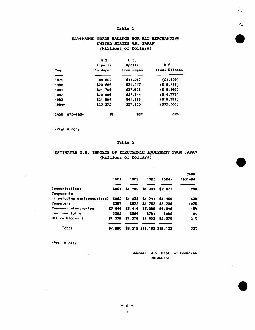
Table 1
ESTIMATED TRADE BALANCE FOR ALL MERCHANDISE UNITED STATES VS. JAPAN (Millions of Dollars)
Year
1975
1980
1981
1982
1983
1984*
CAGR 1975-1984 i1% 20% 39%
• P r e l i m i nory
Table 2
ESTIMATED U.S. IMPORTS OF ELECTRONIC EQUIPMENT FROM JAPAN (Millions of Dollars)
CAGR
1981 1982 1983 1984* 1981-84
U.S.
Exports
to Japan
$9,567
$20.806
$21,796
$20,966
$21,894
$23,575
U.S.
Imports
f rom Japan
$11,257
$31,217
$37,598 $37,744
$41,183
$57,135
U.S. Trade Balance
($1,690)
($10,411)
($15,802)
($16,778)
($19,289)
($33,560)
Communications $961 $1,109 $1,391 $2,077 29% Components
(including semiconductors) $962 $1,233 $1,741 $3,450 53%
Computers $387 $822 $1,762 $3,200 102%
Consumer electronics $3,646 $3,410 $3,985 $6,040 16%
Instrumentotion $592 $566 $701 $985 18%
Office Products $1,338 $1,379 $1,602 $2,370 21%
Total $7,886 $8,519 $11,182 $18,122 32%
•Preliminary
Source: U.S. Dept. of Commerce OATAQUEST
- 4 -
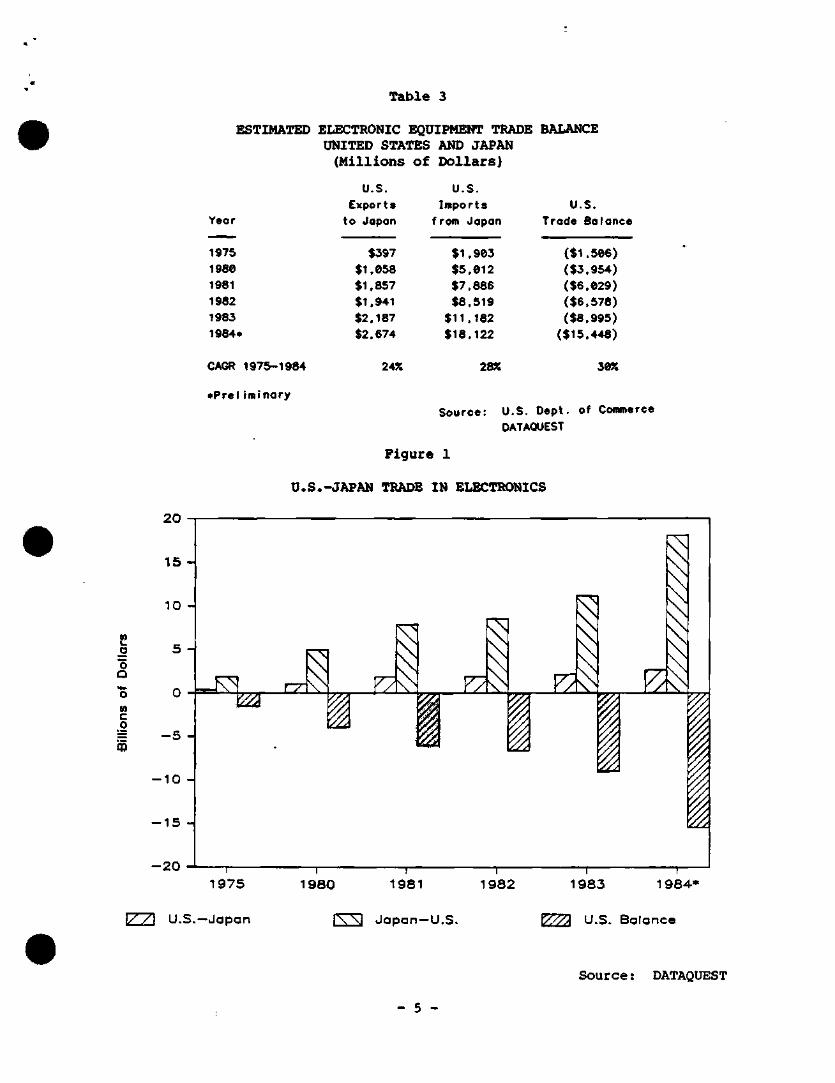
Table 3
m u "o
O
10 c o
'm
ESTIMATED ELECTRONIC EQUIPMENT TRADE BALANCE
UNITED STATES AND JAPAN
(Millions Of Dollars)
Year
1975
1980
1981
1982
1983
1984*
CAGR 197&-1984
•Prelin nary
U.S. Exports
to Japan
$397
$1,058
$1,857
$1,941 $2,187
$2,674
24%
U.S. Imports
from Japan
$1,903
$5,012 $7,886
$8,519
$11,182
$18,122
lex
U.S. Trade Balance
($1,506)
($3,954)
($6,029)
($6,578)
($8,995)
($15,448)
30%
Source: U.S. Dept. of Cownerce
DATAQUEST
Figure 1
U.S.-JAPAN TRADE IN ELECTRONICS
2 0
15 -
10 -
5 -
-5 -
- 1 0 -
•15
- 2 0
^
- ^ rrVK
7q
a K J
I ^ 0
i 1
X
2K
1975
[77n U.S.-Jopan
1980 1981 1982 1983 1984*
( X ^ Japan -U .S . g ^ ^ U.S. Balance
S o u r c e : DATAQUEST
- 5 -
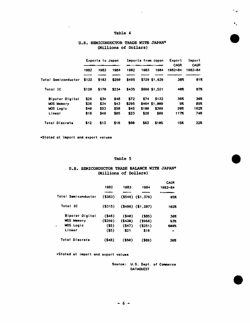
Table 4
U . S . SEMICONDUCTOR TRADE WITH JAPAN* (Mil l ions o f Dol lars)
Exports to Japan Impo r ts from Japan Expo r t Import
CAGR CAGR
1982 1983 1984 1982 1983 1984 1982-84 1982-84
Tota l Semiconduc tor $132 $183 $250 $495 $729 $1 ,626
Tota l IC $120 $170 $234 $435 $666 $1 ,521
B i p o l a r D i g i t a l $26 $34 $48 $72 $74 $133
MOS Memory $36 $34 $43 $295 $464 $1 ,009
MOS Logic $40 $53 $58 $45 $100 $309
L i nea r $ 1 8 $49 $85 $23 $28 $69
Tota l D i s c r e t e $12 $13 $16 $60 $63 $105
3S^
40%
15%
81%
87%
36% 36% 9% 85%
20% 162%
117% 74%
32%
• S t a t e d ot import and expo r t values
T a b l e 5
U . S . SEMICONDUCTOR TRADE BALANCE WITH JAPAN* ( M i l l i o n s Of D o l l a r s )
1982 1983 1984
Totol Semiconductor ($363) ($546 ) ( $ 1 , 3 7 6 )
Tota l IC ($315) ($496 ) ( $ 1 , 2 8 7 )
B i p o l a r O ig i t a l
MOS Memory
MOS Log i c
L i n e a r
Tota l D i s c r e t e
($46) ($40) ($85) ($259) ($430) ($966)
($5) ($47) ($251) ($5) $21 $16
($48) ( $ 5 0 ) ($89)
CAGR
1982-84
95%
102%
36% 93%
609%
36%
• S t a t e d a t import and expo r t volues
Sou rce: U . S . Dept . of Commerce
DATAOUEST
- 6 -
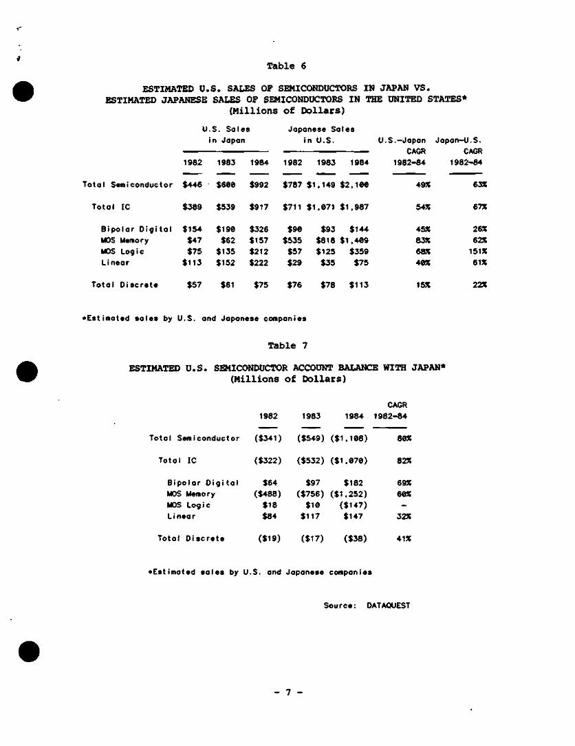
Table 6
ESTIMATED U . S . SALES OP SEMICONDUCTORS IN JAPAN VS. ESTIMATED JAPANESE SALES OF SEMICONDUCTORS IN THE UNITED STATES*
(Millions of Dollars)
U . S . Sales
in Japan
Japonese Sales
in U.S .
1962 1983 1984 1982 1983 1984
U .S . -Japon Japan—U.S.
CAGR CAGR
1982-84 1982-84
Tota l Semiconductor $446 $600 $992 $787 $1 ,149 $ 2 , 1 0 0
Tota l IC $389 $539 $917 $711 $1 , 071 $ 1 , 9 8 7
B i p o l a r D i g i t a l $154 $190 $326 $90 $93 $144
MOS Memory $47 $62 $157 $535 $818 $ 1 , 4 0 9
MOS Logic $75 $135 $212 $57 $125 $359
L inear $113 $152 $222 $29 $35 $75
Tota l D i s c r e t e $57 $61 $75 $76 $78 $113
49%
54X
45%
83%
68%
40%
63%
67%
26%
62%
151%
61%
15% 22%
'Estimated sales by U.S. and Japanese companies
Table 7
ESTIMATED U.S. SEMICONDUCTOR ACCOUNT BALANCE WITH JAPAN*
(Millions of Dollars)
1982 1983
Total Semiconductor ($341) ($549) ($1,108)
Total IC ($322) ($532) ($1,070)
CAGR
1984 1982-84
Bipolar Digital $64 $97 $182
MOS Memory ($488) ($756) ($1,252)
MOS Logic $18
Linear $84
$10 ($147)
$117 $147
Total Discrete ($19) ($17) ($38)
80%
82%
69%
60%
32%
41%
•Estimated sales by U.S. and Japanese companies
Source: DATAQUEST
- 7 -
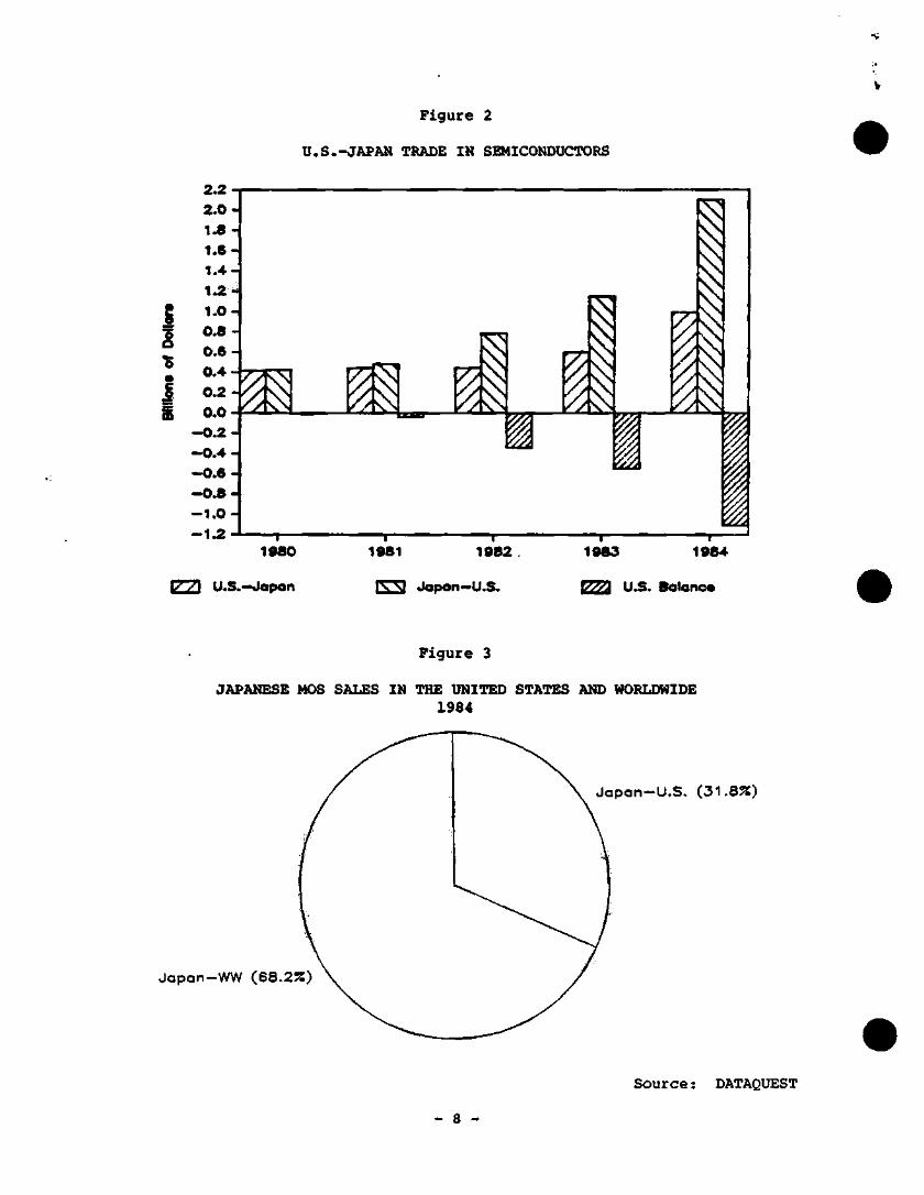
Figure 2
U.S.-JAPAN TRADE IN SEMICONDUCTORS
i i
2.2 2.0-1.8 -1.6-1.4-IJi-1.0 0.8 0.6
0.4 H 0.2 0.0
-0.2--0.4--0.6--0.8--1.0--1.2
m ^5^ m
m P . ^ ^
m i m I
J i
i 1980
CTTI U.S.—Japan
1981 1982 .
fT^ Japan-U.S.
Figure 3
1983 1984
P?^ U.S. Balanc*
JAPANESE MOS SALES IN THE UNITED STATES AND WORLDWIDE 1984
Japan-WW (68.2%)
Japan-U.S. (31.8%)
Source: DATAQUEST
- 8 -
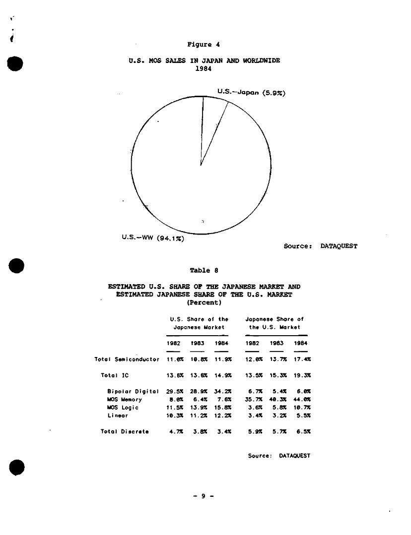
Figure 4
U.S. MOS SALES IN JAPAN AND WORLDWIDE 1984
U.S.—Japan (5.9%)
U.S.-WW (94.1%) Source: DATAQUEST
Table 8
ESTIMATED U.S. SHARE OF THE JAPANESE MARKET AND ESTIMATED JAPANESE SHARE OF THE U.S. MARKET
(Percent)
U.S. Share of the Japanese Market
1982 1983 1984
Japanese Share of the U.S. Market
1982 1983 1984
Total Semiconductor 11.0% ^.SZ 11.9% 12.0^ 13.7% 17.4%
Total IC 13.6% 13.6% 14.9% 13.5% 15.3% 19.3%
Bipolar Digital 29.5% 28.9% 34.2% MOS Memory 8.0% 6.4% 7.6% MOS Logic 11 .5% 13.9% 15.8% Linear 10.3% 11.2% 12.2%
Total Discrete 4.7% 3.8% 3.4%
6.7% 5.4% 6.0% 35 .7% 40.3% 44.0%
3.6% 5.8% 10.7% 3 .4% 3.2% 5.5%
5.9% 5.7% 6.5%
Source: DATAQUEST
- 9 -
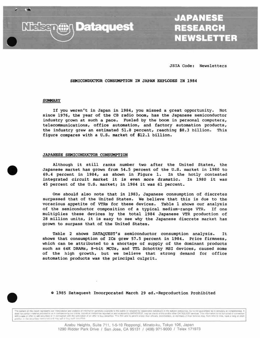
Dataquest JAPANESE RESEARCH NEWSLETTER
JSIA Code: Newsletters
SEMICONDUCTOR CONSUMPTION IN JAPAN EXPLODES IN 1984
SUMMARY
If you weren't in Japan in 1984, you missed a great opportunity. Not since 1976, the year of the CB radio boom, has the Japanese semiconductor industry grown at such a pace. Fueled by the boom in personal computers, telecommunications, office automation, and factory automation products, the industry grew an estimated 51.8 percent, reaching $8.3 billion. This figure compares with a U.S. market of $12.1 billion.
JAPANESE SEMICONDUCTOR CONSUMPTION
Although it still ranks number two after the United States, the Japanese market has grown from 54.5 percent of the U.S. market in 1980 to 69.4 percent in 1984, as shown in Figure 1. In the hotly contested integrated circuit market it is even more dramatic. In 1980 it was 45 percent of the U.S. market; in 1984 it was 61 percent.
One should also note that in 1983, Japanese consumption of discretes surpassed that of the United States. We believe that this is due to the voracious appetite of VTRs for these devices. Table 1 shows our analysis of the semiconductor composition of a typical medium-range VTR. If one multiplies these devices by the total 1984 Japanese VTR production of 28 million units, it is easy to see why the Japanese discrete market has grown to surpass that of the United States.
Table 2 shows DATAQUEST's semiconductor consumption analysis. It shows that consumption of ICs grew 57.5 percent in 1984. Price firmness, which can be attributed to a shortage of supply of the dominant products such as 64K DRAMs, 8-bit MCUs, and TTL Schottky MSI devices, caused some of the high growth, but we believe that strong demand for office automation products was the principal culprit.
o 1985 Dataquest Incorporated March 29 ed.-Reproduction Prohibited
The content of this report represents our interpretalon and anaIysis ot information generally available to the public or released by responsible individuals in the subject companies, but is not guaranteed as to accuracy or completeness. It does not contain material provided to us in confidence by our clients Individual companies reported on and analyzed by DATAQUEST, may be clients o( this and/or other DATAQUEST services This information is not furnished in connection witfi a sale or offer to sell securities or in connection with the solicitation of an offer to buy securities This firm and its parent and/or their officers, stockholders, or members of their families may, from time to time, have a long or short
Azabu Heights, Suite 711, 1-5-10 Roppongi, Minato-ku, Tokyo 106, Japan 1290 Bidder Park Drive / San Jose, CA 95131 / (408) 971-9000 / Telex 171973
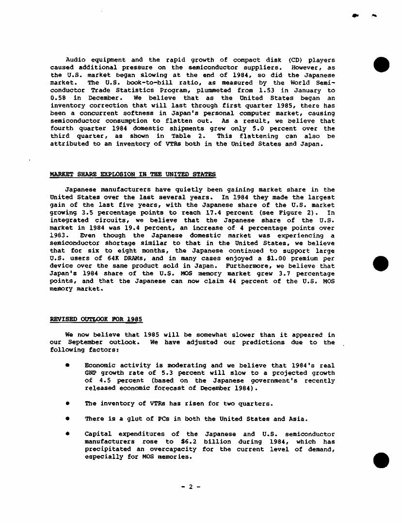
Audio equipment and the rapid growth of compact disk (CD) players caused additional pressure on the semiconductor suppliers. However, as the U.S. market began slowing at the end of 1984, so did the Japanese market. The U.S. book-to-bill ratio, as measured by the World Semiconductor Trade Statistics Program, plummeted from 1.53 in January to 0.58 in December. We believe that as the United States began an inventory correction that will last through first quarter 1985, there has been a concurrent softness in Japan's personal computer market, causing semiconductor consumption to flatten out. As a result, we believe that fourth quarter 1984 domestic shipments grew only 5.0 percent over the third quarter, as shown in Table 2. This flattening can also be attributed to an inventory of VTRs both in the United States and Japan.
MARKET SHARE EXPLOSION IN THE UNITED STATES
Japanese manufacturers have quietly been gaining market share in the United States over the last several years. In 1984 they made the largest gain of the last five years, with the Japanese share of the U.S. market growing 3.5 percentage points to reach 17.4 percent (see Figure 2). In integrated circuits, we believe that the Japanese share of the U.S. market in 1984 was 19.4 percent, an increase of 4 percentage points over 1983. Even though the Japanese domestic market was experiencing a semiconductor shortage similar to that in the United States, we believe that for six to eight months, the Japanese continued to support large U.S. users of 64R DRAMs, and in many cases enjoyed a $1.00 premium per device over the same product sold in Japan. Furthermore, we believe that Japan's 1984 share of the U.S. MOS memory market grew 3.7 percentage points, and that the Japanese can now claim 44 percent of the U.S. MOS memory market.
REVISED OUTLOOK FOR 1985
We now believe that 1985 will be somewhat slower than it appeared in our September outlook. We have adjusted our predictions due to the following factors:
• Economic activity is moderating and we believe that 1984's real GNP growth rate of 5.3 percent will slow to a projected growth of 4.5 percent (based on the Japanese government's recently released economic forecast of December 1984) .
• The inventory of VTRs has risen for two quarters.
• There is a glut of PCs in both the United States and Asia.
• Capital expenditures of the Japanese and U.S. semiconductor manufacturers rose to $6.2 billion during 1984, which has precipitated an overcapacity for the current level of demand, especially for MOS memories.
- 2 -
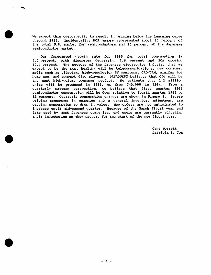
We expect this overcapacity to result in pricing below the learning curve through 1985. Incidentally, MOS memory represented about 30 percent of the total U.S. market for semiconductors and 20 percent of the Japanese semiconductor market.
Our forecasted growth rate for 1985 for total consumption is 7.0 percent, with discretes decreasing 2.6 percent and ICs growing 10.4 percent. The sectors of the Japanese electronics industry that we expect to be the most healthy will be telecommunications, new consumer media such as Videotex, high-resolution TV monitors, CAD/CAM, minifax for home use, and compact disc players. DATAQUEST believes that CDs will be the next high-volume consumer product. We estimate that 1.2 million units will be produced in 1985, up from 740,000 in 1984. From a quarterly pattern perspective, we believe that first quarter 1985 semiconductor consumption will be down relative to fourth quarter 1984 by 11 percent. Quarterly consumption changes are shown in Figure 3. Severe pricing pressures in memories and a general inventory adjustment are causing consumption to drop in value. New orders are not anticipated to increase until mid-second quarter. Because of the March fiscal year end date used by most Japanese companies, end users are currently adjusting their inventories as they prepare for the start of the new fiscal year.
Gene Norrett Patricia S. Cox
- 3 -
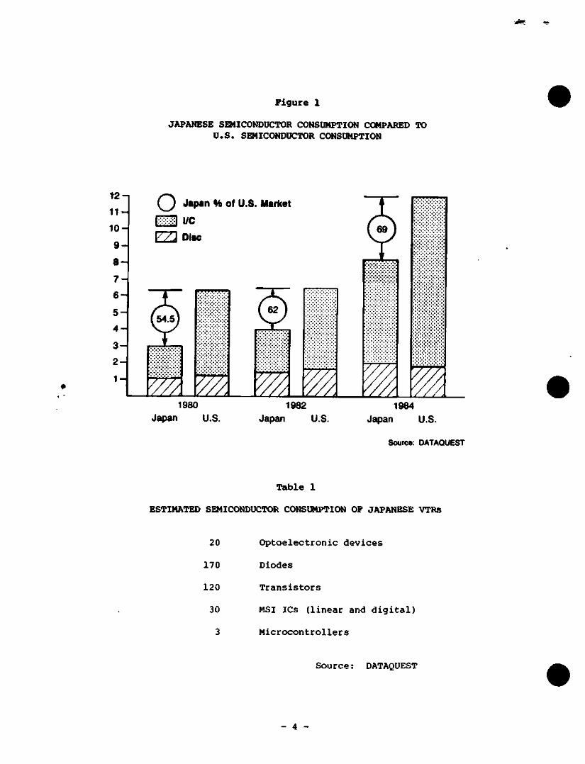
Figure 1
JAPANESE SQ*ICONDUCTOR CONSUMPTION COMPARED TO U.S. SEMICONDITCTOR CONSUMPTION
t 2 - |
1 1 -
1 0 -
9 -
8 -
7 -
6 -
5 -
4 -
3 -
2 -
' \
Q Japan % of U.S. Market
i H i / c ZZ2 D'M
vTTTwrv^m
TZ
g ^
1980 Japan U.S.
1982 Japan U.S.
1984 Japan U.S.
Source: DATAQUEST
Table 1
ESTIMATED SEMICONDUCTOR CONSUMPTION OF JAPANESE VTRs
20 Optoelectronic devices
170 Diodes
120 Transistors
30 MSI ICs (linear and digital)
3 Microcontrollers
Source: DATAQUEST
- 4 -
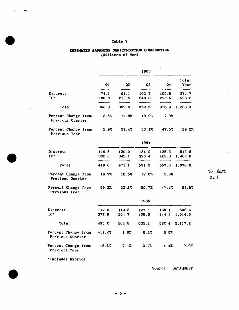
Table 2
ESTIMATED JAPANESE SEMICONDUCTOR CONSUMPTION (Billions of Yen)
1983
Discrete IC*
Total
Percent Change from Previous Quarter
Ql
74.1 188.8
262.9
2.5%
Q2
91.1 218.5
309.6
17.8%
Q3
103.7 248.8
352.5
13.9%
Q4
105.8 272.5
378.3
7.3%
Total Year
374.7 928.6
1.303.3
Percent Change from Previous Year
5.9% 29.4% 33. 1% 47.5% 29.2%
1984
Discrete IC*
Total
Percent Change from Previous Quarter
116.6 302.0
418.6
10.7%
129.0 342.1
471.1
12.5%
134.9 396.4
531.3
12.8%
135.3 515.8 422.3 1.462.8
557.6 1,978.6
5.0% 'zy^ Cecto
7 cl
Percent Change from Previous Year
59.2% 52.2% 50.7% 47.4% 51 .8%
1985
Discrete IC
Total
Percent Change from Previous Quarter
117.6 377.6
495 2
-11.2%
119.8 384.7
504.5
1.9%
127 408.
535.
6.
. 1 0
1
1%
138.1 502.6 444.3 1.614.6
582.4 2.117.2
8.8%
Percent Change from Previous Year
18.3% 7. 1% 0.7% 4.4% 7.0%
•Includes hybrids
Source: DATAQUEST
- 5 -
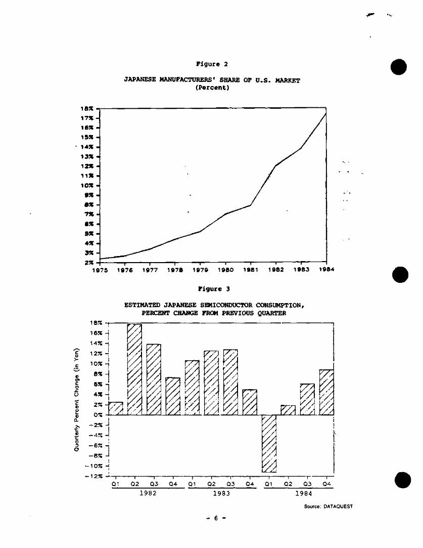
Figure 2
JAPANESE MANUFACTURERS' SHARE OF U . S . MARKET (Percent)
1BX
197S 1976 1977 1978 1979 1980 1981 1982 1983 1984
Figure 3
c o >-
«> Oi c o X
o c t> u u o a. 9 •t O 3
o
18%
16%
14%
12%
10%
8%
6%
4%
2%
O%
- 2 %
- 4 %
— O/-©
- 8 %
-10%
-12%
ESTIMATED JAPANESE SEMICONDUCTOR CONSUMPTION, PERCENT CHANGE FROM PREVIOUS QUARTER
^
/.Ai yy
^Z
mML
•//, •'A
1982 1983 1984
Source: DATAQUEST
- 6 -
Dataquest JAPANESE — RESEARCH NEWSLETTER
JSIA Code : N e w s l e t t e r s
SUCCESSFUL INTELLIGENCE GATHERING: DATAQUEST'S RECIPE
Gene N o r r e t t , V i c e P r e s i d e n t and D i r e c t o r of D a t a q u e s t ' s J a p a n e s e S e m i c o n d u c t o r I n d u s t r y S e r v i c e , a d d r e s s e d S o u t h c o n ' 8 5 on m a r k e t r e s e a r c h and i n t e l l i g e n c e g a t h e r i n g t e c h n i q u e s . The t e x t o f t h e s p e e c h i s r e p r i n t e d h e r e .
Gene N o r r e t t
1985 D a t a q u e s t I n c o r p o r a t e d March 28 e d . - R e p r o d u c t i o n P r o h i b i t e d
The conlent of this report represents our interpretaion and analysis of information generally available to the public or released by responsible individuals in the subject companies, but is not guaranteed as to accuracy or completeness It does not contain material provided to us in confidence by our clients Individual companies reported on and analyzed by DATAOUEST, may be clients of this and/or other DATAOUEST services This information is not furnished in connection with a sale or offer to sell securities or in connection with the solicitation of an offer lo buy securities This firm and its parent and/or their officers, stockholders, or members of their families may, from time to time, have a long or short position in the securities mentioned and may sell or buy such securities
Azabu Heights, Suite 711, 1-5-10 Roppongi, tVlinato-ku, Tokyo 106, Japan 1290 Bidder Park Drive / San Jose, CA 95131 / (408) 971-9000 / Telex 171973
Good afternoon, ladies and gentlemen.
First, I want to thank the leader of this session and a good friend, Betty Prince from Motorola, for giving me this opportunity to address you today. I also want to thank the directors of Southcon 1985 for providing the forum to make this presentation.
I want to address the topic of Successful Intelligence Gathering from a high-technology market research perspective. This viewpoint is a natural one for both you and me because of our common interest in the world electronics market. Further, I will address this topic in the context of providing you, the worldwide marketing managers, with an insight into marketing your electronic products abroad, in accordance with the theme of this session. (Slide 1).
My analysis will cover four major points: the What, Why, Where, and finally, the How to, of intelligence acquisition.
In preparing this speech, I was reminded of some statements made by the great Silicon Valley prophet, James R. Riley. In case some of you don't know Jim, he started the Dataquest Semiconductor Industry Service in 1974 and directed its growtn for many years. Before that, Jim was president of Signetics and then Intersil. Jim has many one-liners that very often help to crystallize ethereal concepts. For example.
What's a good tax shelter? Jim's answer: "Make a lot of money."
What is the best overall methc of making a decision? Jim quickly responds "Listen to what your gut is telling you."
"Why use Dataquest or other market research companies for decision support? Jim's answer is, "Are you good at explaining an Edsel to your stockholders?"
I believe that what Jim is saying here is that information or intelligence is critical for success. The most important thing for business and professional people to have, and the most difficult thing to find, is intelligence.
Now let's look at each of the major points in detail: (Slide 2).
The first point is "What Is Intelligence?". Webster defines intelligence as
First: The ability to learn or understand or deal with new or trying situations
Second: The ability to apply knowledge in order to manipulate one's environment
- 2 -
Therefore, to paraphrase Webster, I would say that intelligence is both the acquisition of hard facts on a given topic and the cogent use of these facts for successful decision making.
The fundamental knowledge that is needed to market your products abroad, especially in Japan, is:
1. What is the market potential for your product (i.e., total available market, past and future)?
2. Who are your potential customers?
3. Who are your competitors, what are their relative sizes, and what are their strengths and weaknesses?
4. What are the price trends of competing products?
5. What is the best method of distribution: (a) direct sales, (b) agents or reps, (c) trading or distributing company?
6. What are the major trade journals for promotion?
7. What cultural differences are important and are there any language barriers?
There are, of course, many more considerations, but once the answers to these questions are answered, then you, as world marketing managers, can make decisions that will lead to successful penetration of international markets. (Slide 3)
"Why Use Intelligence?" is the second major question. Obviously, one answer would be to minimize failures and maximize success. Jim Riley's answer would be "How good are you at explaining the Edsel to your stockholders?" Unfortunately, I believe that today there are only a very limited number of decision makers who have come to the conclusion that "In the Valley of the Blind, the one-eyed man is King." To support this opinion, I cite a study published in the prestigious Harvard Business Review. It revealed that only about 8 percent of the businesses represented by 1,200 survey participants had a department with employees trained to gather and analyze information about competitors.
In explaining the purpose of intelligence to my clients, I tell them that information should be considered as valuable a resource as capital and labor. Information has been historically underpriced, underutilized, and its contribution underrated. The question of why we use intelligence seems basic to me, but again, this is my business. But for many American executives, "seat of the pants" decision making is a way of life. The Japanese executives are much different. Furthermore I believe that there is a strong relationship between the amount of information that the Japanese gather on western technology and the trade balance between Japan and the West. (Slide 4)
- 3 -
When I was starting the Japanese Semiconductor Industry Service, I came across two very interesting statistics relating to the unbalanced level of information trade. The first one is that from a translation perspective, for every page of Japanese translated into English, there are 100 pages of English translated into Japanese. I don't know the breakdown of the text contents, but I would guess that for electronics the ratio is significantly larger. The second statistic relating to information trade is that the largest users of the National Technical Information Service (NTIS) are the Japanese. In fact, one official of the NTIS told me that the Japanese keep it solvent. The NTIS contains more than 500,000 publicly available reports on research projects sponsored by federal agencies and some state and local governments.
I can further cite another very specific example of how the Japanese value information. When I was working for Motorola as Manager of Market Research and Business Analysis, I served as Motorola's rep to the SIA. As chairman of the Statistics Committee, which met twice per year to prepare a consensus three-year forecast of the industry, I visited the Electronic Industry Association of Japan. In my discussions with this group, they told me that they had a similar coiranittee to the committee that I was chairman of. They advised me that their committee meets monthly to discuss the status of the Japanese industry, and in some cases might meet more frequently than monthly. Certainly you can see that this level of information on the status of their industry is significantly higher than that of the SIA.
At Dataquest, as reporters and analyzers of market competition, we frequently compare this competition to a game of cards. Due to the extensive information advantage of the Japanese, they generally know 50 of the 52 playing cards whereas western competitors know only 2 of the 52, a significant disadvantage, I believe.
Anyone who has done research projects knows that libraries are a fundamental source of information. They contain journals, surveys, and annual reports. Other sources are colleagues and, of course, research companies. Dataquest is relatively new at decision support but its parent companies, A.C. Nielsen Company and Dun and Bradstreet, have been educating leaders of industry on the importance of sound information and have been delivering this information to an ever-increasing population for many years. This delivery is supplemented with application related material because we know that today's executives need interpretation of information even more than the data itself.
Today, A.C. Nielsen, Dataquest's direct parent, is operating in 28 countries, employs more than 22,000 people worldwide, and serves 17,000 clients. Its 1983 sales were more than $680 million and its revenues have grown over the last ten years at a rate of 17.8 percent. Moreover, Dun and Bradstreet, which purchased A.C. Nielsen in September 1984, is a $1.5 billion information company. D&B has 28,000 employees and is the largest provider of business services and information in the private sector. (Slides 5 and 6)
- 4 -
As this slide shows. Dun and Bradstreet's business spans business information services, publishing, and marketing services. These businesses are designed to support many of the fastest growing sectors of the world's economies. The specific areas of marketing, market research, and product development are the most significantly supported by Dun and Bradstreet. (Slide 7)
Furthermore, Dataquest, like A.C. Nielsen and Dun and Bradstreet, is also an information company. Dataquest was started in 1972 and has grown into a company with 300 employees and more than 2,000 clients. We specialize in the high-technology industries of semiconductors, computers and computer peripherals, telecommunications, and design and manufacturing automation. Based in Silicon Valley we are dedicated to providing a unique consulting service to our clients, founded upon intelligence gathering and analysis. (Slide 8)
I believe the answer to the question, "where to find information" is on the surface an obvious one. We, at Dataquest, use the information sources mentioned in slide 9 as our principal sources of published information. However, to be able to get specific detail on the industries, products, companies, technologies, etc. we, at Dataquest, have developed a collection of the most important information sources and in soriie cases sources of sources on the industries that we follow. (Slide 9)
From companies' annual reports and Securities and Exchange Commission Files we are able sometimes to gather not only fundamental information on companies but also very valuable intelligence on the market in which these companies participate. I want to call your attention to Electronic Association reports. In many cases the associations in the United States, Europe, Japan, and Asia have statistical committees that are chartered to provide their members with very high quality data and analyses. We thoroughly know and utilize these data bases. (Slide 10)
We also find that utilizing other research companies' published reports is a valuable help in our analyses. These companies include, of course, those on Wall Street.
Further we are making increasing use of on-line data bases and I recommend you become familiar with the data bases that pertain to your industry. One major data bank vendor is CompuServe. The second is Dialog.
Finally, in our library we have the proceedings from the major trade shows and also our analysts' trip reports, which summarize the major happenings at these shows.
The last question, namely how to gather information is the most difficult one. (Slide 11)
In order to develop this point, I'll share with you the recipe of the Japanese Semiconductor Industry Service (JSIS), which I direct.
- 5 -
In setting up the service, we were faced with the challenge of providing a comprehensive data base on the Japanese market, technologies, and companies, including their strategies, capacities, patent applications, equipment/materials that they use, and finally their products. (Slide 12)
To do this, I set up two offices to gather information, conduct analyses, and interact with the clients.
I believe that in order to be in the international intelligence business, one must gather information locally by locals. As such, JSIS has staff in both Tokyo and in San Jose, the two centers of the competing semiconductor industries. We also maintain very good relationships with companies on the "Silicon Plain" in Texas and in the "Silicon Desert" in Phoenix. (Slide 13)
Our analysts gather both published and unpublished data and incorporate them into a total data base.
I have already shown you the published data sources. The unpublished information comes from our network of industry and government contacts that have been established over the years. When a contact is made by an analyst, manager, V.P., or President at Dataquest, a contact report is generated and sent to our central library for processing. (Slide 14)
The library receives the contact report and it is computerized and filed by subject, key word, and company. Through electronic mail, members of the Dataquest staff can see this information immediately for action and follow-up.
Direct interaction with our computerized data base is available to clients of our service. The clients can also interact with analysts through the inquiry privilege that is included in the services. These inquiry privileges allow clients to interrogate the analysts on subjects pertinent to the data base; response time is generally within one day. The need for immediate response to these unique questions drives us to do a great deal of in-depth analysis. (Slide 15)
The Japanese Semiconductor Industry Service data base is tied into Other regional semiconductor data bases, and Dataquest is in the process of linking all its services into a macro data base. This linking will enable the analysts to do significantly more research and provide much better service to the clients. Our world semiconductor data base is supported by 50 people around the world, which constitutes the world's largest group of experts that continuously monitor this very rapidly changing industry. (Slide 16)
- 6 -
Dataquest's Japanese Semiconductor Industry Service monitors technology trends in materials, components, and semiconductor manufacturing equipment. We have the most extensive data base on Japanese factories so that statements can be made on capacity levels and changes in capacity. We also report on patent trends through this data base. Patent information is available by company, by technology, and by product. We do market share and product portfolio analyses from our company profile data, and finally, the data base contains the Japanese market dissected by end-user market by product by company. A very ambitious project.
To summarize, I have addressed the what, where, why, and the how to of successful intelligence gathering for the purpose of marketing products abroad. The most critical thought to remember is that the progress of information gathering should not be passive, but interactive with experts. We at Dataquest believe that it is not only data that is needed, but a unique perspective that will enable you, as decision makers, to test the validity of your assumptions. We want you to succeed and we believe that our research and analysis will help to provide this success.
Thank you.
- 7 -
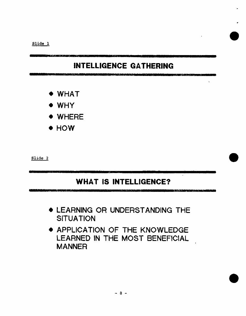
S l i d e 1
mmmmmumMMummummmmimm, KummmmmmmuimBmm^mmmmmm
INTELLIGENCE GATHERING
• WHAT
• WHY
• WHERE
• HOW
S l i d e 2
WHAT IS INTELLIGENCE? wamtam^mmmmmmmmammmammmeaiumuKamasiammfammKuamimmiam
• LEARNING OR UNDERSTANDING THE SITUATION
• APPLICATION OF THE KNOWLEDGE LEARNED IN THE MOST BENEFICIAL MANNER
- 8 -
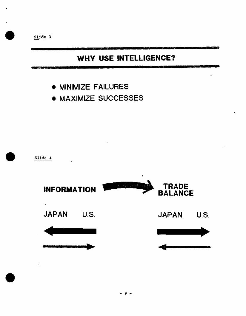
S l i d e 3
WHY USE INTELLIGENCE?
• MINIMIZE FAILURES
• MAXIMIZE SUCCESSES
S l i d e 4
INFORMATION TRADE BALANCE
JAPAN U.S. JAPAN U.S.
- ^
- 9 -
S l i d e 5
A.C. NIELSEN COMPANY REVENUES (Fiscal Years Ended August 31st}
liBii inwi laB igg i ^ an^
1934 1983
S l i d e 6
k'mnmu mmtsmt
DUN & BRADSTREET
REVENUES
INCOME
NET INCOME
PER SHARE
1982
1,361 147
2.53
1983
1.510
167
2.97
1984 (Forecast)
1.700
185
3.20
- 10 -
S l i d e 7
Products and Services
• '• •
i * •
• •
Business Infonnalloii Services Dun & Bradstreet Credit Services D u n & B rads treet International tCiwdH Srn>ic« and Commeraal collections)
D&B Computing Services Dun & Bradstreet Plan Services Dun & Bradstreet Commercial Collections DunsPlus McCormack & Dodge TSI International Zytron PuiilisUiig Reuben H. Donnelley Moody's Investors Service Official Airline Guides Technical Publishing Dun & Bradstreet Business Education Services Technical Data Resources Marlteting Services Donnelley Marketing Dun's Marketing Services Dun & Bradstreet International iMarkeUngt Donnelley Marketing Information Services Financial Services industry Group Salesnet
Some of tlw nujiy fields of econonlc activity served by
Tiie Dun & Bradstreet Corporation:
• Advertising, Direct Mail and Telemarketing • Airline and Travel Infonnation and Planning
• Banking and Insurance • Commercial Credit Information and Collection Services
• Computer Services. Software Programs and Applications • Economic and Fmancial Analysis and Investment Planning
# Human Resources Management /including personnel education and aainingl
* Manufacturing. Distribution and Purchasing • Marketing. Market Research and Product Development
• Reference Material for Schools and Libraries • Sales and Sales Management Strategic Planning
- 11 -
Slide 8
KBasaB5i5^igaaaitiKgig5gfi»8ira!BiaEaaawai5seiiaB
DATAOUEST
• STARTED IN 1971
• 2000 CLIENTS
• REVENUE GROWTH OF 20% PER YEAR
• SPECIALIZING IN HIGH TECHNOLOGY MARKET RESEARCH
S l i d e 9
SOURCES OF ELECTRONICS INFORMATION
• ANNUAL REPORTS AND SEC FILINGS BY COMPANIES
• WORLD GOVERNMENT REPORTS AND STATISTICS
• DATAQUEST NOTEBOOKS AND NEWSLETTERS « TRADE MAGAZINES
• WORLDWIDE PATENT RECORDS
• ELECTRONIC ASSOCIATION'S DATA AND REPORTS
- 12 -
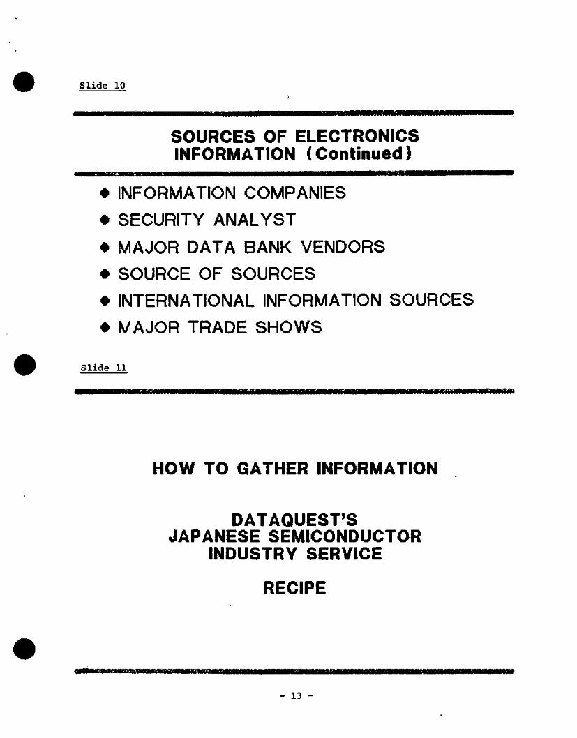
S l i d e 10
SOURCES OF ELECTRONICS INFORMATION (Continued)
•^•IIWilil(iMIM»»WH»»W»MMri«BMMM«««WWW^ M'llllllil IWWIIIWWWIII1ITI ir llllllBMiiMMiWiaBMWaWMWMMM^
• INFORMATION COMPANIES
• SECURITY ANALYST
• MAJOR DATA BANK VENDORS
• SOURCE OF SOURCES
• INTERNATIONAL INFORMATION SOURCES
• MAJOR TRADE SHOWS
S l i d e 11
•••^MamBamfiimMMMwaMMwnmfTiwfBmamaBB^
HOW TO GATHER INFORMATION
DATAQUEST'S JAPANESE SEMICONDUCTOR
INDUSTRY SERVICE
RECIPE
- 13
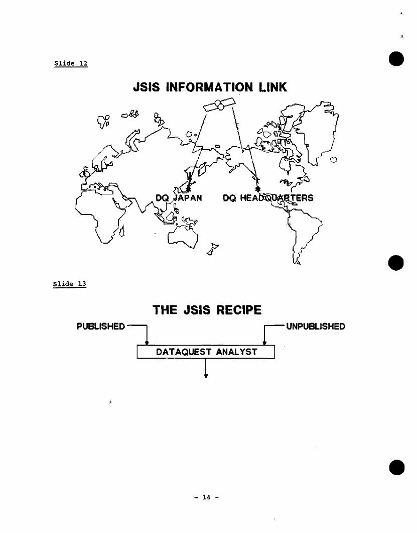
S l i d e 12
JSIS INFORMATION LINK
oS^ £1 / \
yf^Uo^l \ i^-'H
DQVAPAN DQ HEASgp^TERS
u. S l i d e 13
PUBLISHED
THE JSIS RECIPE
DATAQUEST ANALYST
UNPUBLISHED
- 14 -
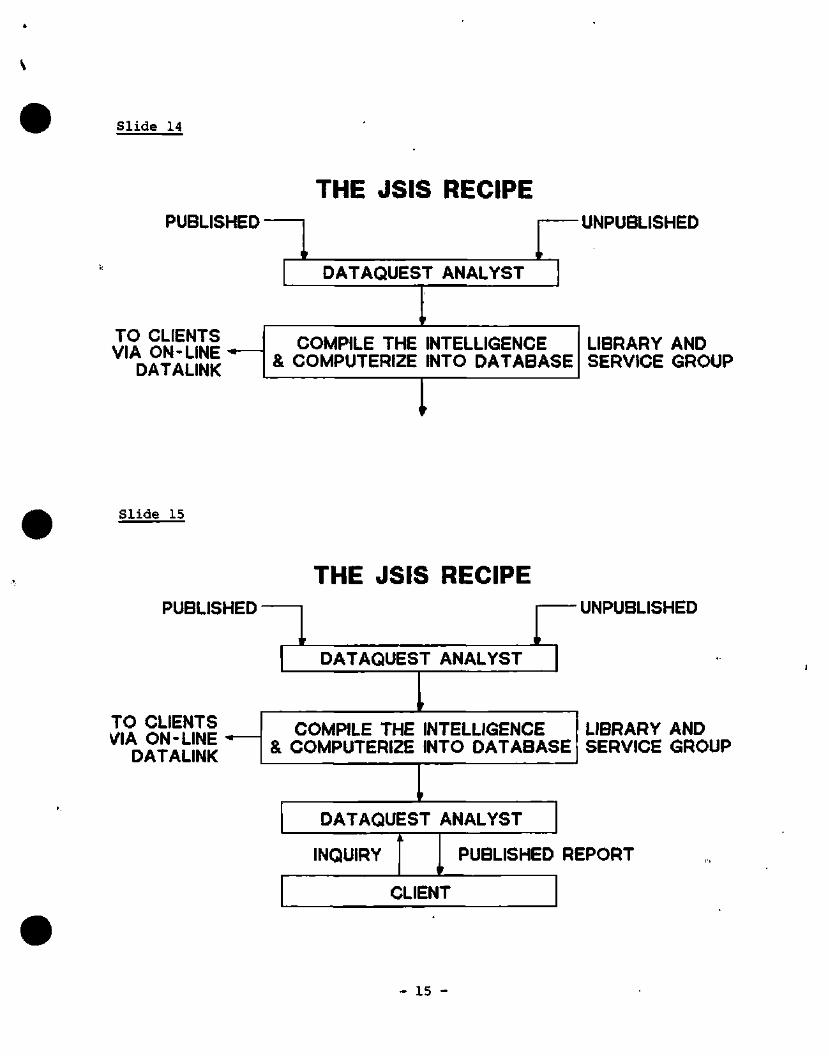
Sl ide 14
THE JSIS RECIPE PUBLISHED UNPUBLISHED
DATAQUEST ANALYST
TO CLIENTS VIA ON-LINE
DATALINK
COMPILE THE INTELLIGENCE & COMPUTERIZE INTO DATABASE
LIBRARY AND SERVICE GROUP
Sl ide 15
PUBLISHED
TO CLIENTS V\A ON-LINE
DATALINK
THE JSIS RECIPE UNPUBLISHED
DATAQUEST ANALYST
COMPILE THE INTELLIGENCE & COMPUTERIZE INTO DATABASE
LIBRARY AND SERVICE GROUP
DATAQUEST ANALYST
INQUIRY PUBLISHED REPORT
CLIENT
- 15 -
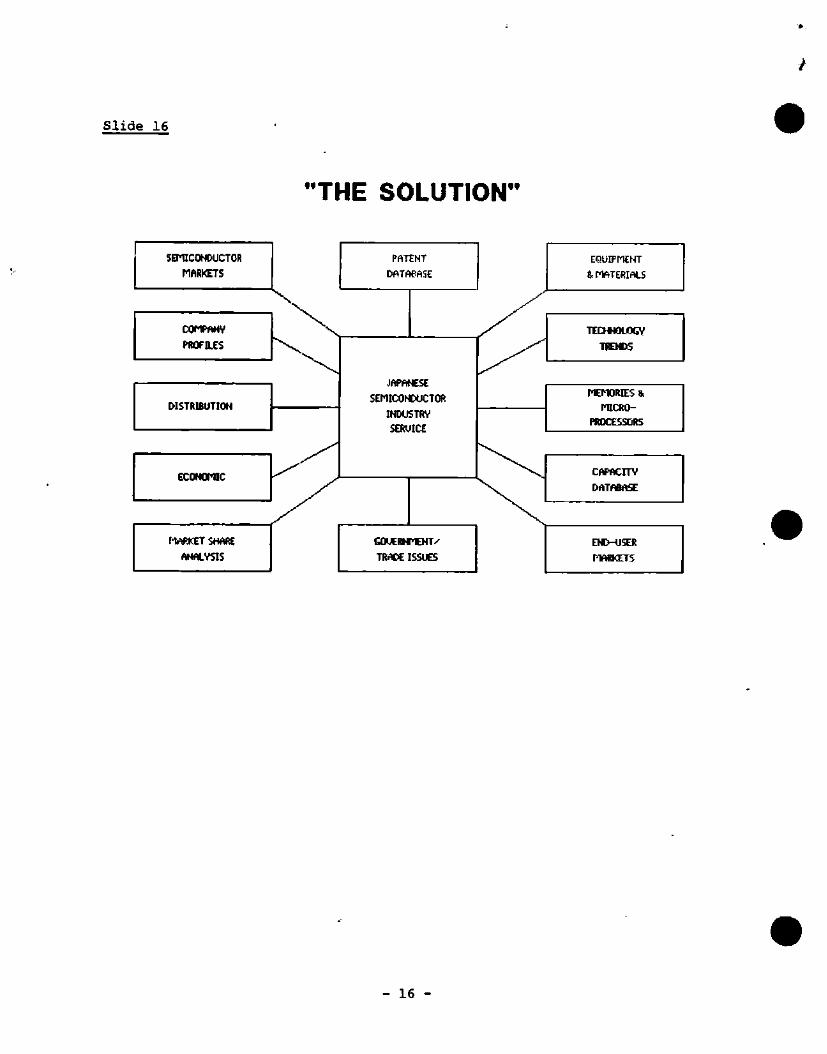
S l i d e 16
f f THE SOLUTION"
SETUCONDUCTOR
MfillKETS
COnPfIMV
PROFILES
DISTRIBUTION
ECDHOniC
r'lrlRKET SHftRE
flNflLVSIS
X
- - ^
PATENT
DftTAeflSE
JAPANESE
SEMICONDUCTOR
INDUSTRV
SEROICE
GOtJERHI^NT^
TRrtDE ISSUES
y y ^
EQUIP PUNT
fc MATERIALS
TECHHOLOGV
TRENDS
ntnoRiES li.
NlCfiO-
PJtOCESSDRS
CAPftCITV
DrtTftBflSE
END-USER
rWRKETS
- 16 -
Dataquest JAPANESE RESEARCH NEWSLETTER
JSIA Code: Newsletters
NEW TRENDS IN JAPANESE SEMICONDUCTOR DISTRIBUTION
INTRODUCTION
The Japanese semiconductor distribution market, thought to be the most complex of all the major world markets, has undergone significant change over the last five years. DATAQUEST believes that many of the leading semiconductor manufacturers are increasing their use of distribution as a major means of market penetration. For example, semiconductor resales by Hitachi's top five distributors have grown at a compound annual growth rate (CAGR) of 68.6 percent over the last five years.
DATAQUEST's Japanese Semiconductor Industry Service (JSIS) has developed a comprehensive data base on semiconductor distribution and consumption in Japan. We have analyzed the market by major semiconductor distributors' total resales and by the major distributors' sales for the top six semiconductor manufacturers in Japan. We have also compared Japanese methods of distribution with those of the United States.
DISTRIBUTOR RESALES
Table 1 lists resales for the top 50 semiconductor distributors in Japan, from 1979 through 1984.
The following points can be observed from this table:
• The number one distributor, Ryosan, lost market share from 1982 to 1984, with 10.6 percent of total distributor resales in 1982 decreasing to 8.9 percent in 1984; however, Ryosan experienced an overall CAGR of 21.9 percent.
• The market share of the top ten distributors decreased from 49.4 percent of total resales in 1982 to 47.9 percent in 1984.
© 1985 Dataquest Incorporated March 26 ed.-Reproduction Prohibited
The content of this report represents our interpretaion and analysis of information generally available to the public or released by responsible individuals in the subject companies, but is not guaranteed as to accuracy or completeness It does not contain material provided to us in confidence by our clients Individual companies reported on and analyzed by DATAQUEST, may be clients of this and/or other DATAOUEST services This Information is not furnished in connection with a sale or offer to sell securities or in connection with the solicitation of an offer to buy securities This firm and its parent and/or their officers, stockholders, or members of their families may, from lime to time, have a long or short position in the securities mentioned and may sell or buy such securities.
Azabu Heights, Suite 711, 1-5-10 Roppongi, Minato-ku, Tokyo 106, Japan 1290 Bidder Park Drive / San Jose, CA 95131 / (408) 971-9000 / Telex 171973
• The smaller distributors are growing significantly faster than the large distributors. While most of the top ten grew at CAGRs less than the average 29.4 percent, many of the smaller distributors grew much faster. Prime examples of this are O.S. Seiki, number 11, at 45.9 percent, and Koshida Shokoh, number 38, at 43.1 percent.
• Four of the top five distributors handle NEC parts.
• Only two of the top ten distributors, Marubun and Tokyo Electron, handle U.S. semiconductor manufacturers' lines
An interesting observation of Table 2 is that from 1979 to 1984, distribution resales as a percentage of total Japanese semiconductor consumption averaged about 43 percent. DATAQUEST believes that in the United States, distribution resales average about 30 percent of total semiconductor consumption.
A second major point that can be seen from this table is that distribution is increasing in importance as a method of going to market. Hitachi is a case in point. Hitachi's major distribution resales grew a whopping 68.6 percent CAGR from 1979 to 1984. This overall trend is a reflection of the increasing pervasiveness of semiconductors in Japan as well as the world. It is also due to the fact that Japanese distributors have recently become more aggressive in exporting VLSIs to the United States and Europe.
Table 3 lists resales by the top five distributors for each of the six major suppliers in the Japanese market.
This table illustrates the following:
• Total distributor sales for these six companies grew close to overall distributor resales growth, at a CAGR of 28.6 percent from 1979 to 1984.
• Hitachi experienced skyrocketing growth, with its distributor sales increasing at a CAGR of 68.6 percent. We believe that Hitachi has made a major strategic change in its path to market, with a heavy emphasis on distribution.
• The top six suppliers' percentage of total distribution resales declined from 1979 to 1984. We believe that smaller suppliers are increasing their use of distribution as a means of getting to market and therefore their distribution sales are growing faster than those of the top six suppliers.
Distribution Methods
Table 4 compares distribution in the United States and Japan. (Europe is intentionally excluded from this comparison because of the lack of homogeneity in the European marketplace. We believe that Europe
- 2 -
must be examined on a country-by-country basis.) Table 4 makes many comparisons between the two competing marketplaces; however, the most important difference is the fact that in Japan, an exclusive distributor handles only one major semiconductor manufacturer because these distributors have very close financial relationships with the semiconductor manufacturers. There are independent distributors in Japan that represent competing manufacturers, but their intent is to represent manufacturers whose products are more complementary than competitive.
We believe that in Japan, a distributor's average order size per device type is almost twice that in the United States. In the United States, a distributor with 150,000 end customers and an average order size of $500 is not uncommon. In Japan there are less than 60,000 end customers and the average order size is $1,200 ([280,000).
In the United States, the major U.S. semiconductor manufacturers sell an average 25 to 35 percent of their domestic business through distributors, and some large manufacturers such as National Semiconductor and AMD use distribution as their primary sales channel. We believe that these companies sell more than twice the average through distribution. In Japan, on the other hand, the top two manufacturers, NEC and Hitachi, sell 95 percent and 60 percent, respectively, of their noncaptive domestic business through distribution.
There are other striking differences in the general methods of doing business through distribution. Japanese equipment manufacturers tend to use the semiconductor distributors as inventory staging locations in order to carry significantly lower inventories. The Japanese semiconductor manufacturers also use the distributors in the same way in order to provide a very high level of service and very quick turnaround on delivery. And in many cases, a Japanese end user will negotiate with a distributor for a fixed price for a given quantity regardless of the unit quantity on an order. This is much different from the United States where prices are most always quoted strictly on a given unit quantity per device or a total unit quantity per order.
Although there are comparatively fewer end customers in Japan, there is a significantly larger (ten times) number of second- and third-tier distributors. This is due to the difference in the makeup of the two electronics industries. In the United States, semiconductor manufacturers tend to grant distributor franchises on a regional or a national basis. However, they do not always give their distributors franchises for all locations, because they want to limit the number of distributors in each territory. In Japan, the granting of franchises is very complex. They may be granted on an area basis or on a given customer basis. There could be a situation where a specific distributor has one major customer with many ship-to locations in a region and only a very limited geographic region to cover because of the importance of this one major customer to the semiconductor manufacturer. In the United States, the largest distribution markets are in the west (principally California) and the mid-Atlantic regions. In Japan, the largest regions are Kanto (Tokyo and Yokohama) and Kinki (Osaka, Kyoto, and Nara).
- 3 -
The average annual sales budget for a typical outside salesperson in a U.S. distributorship is estimated to be $2.5 million. This includes all products that the distributor sells; i.e., semiconductors, passive components, and systems. His counterpart in Japan is responsible for an estimated $4.8 million, almost twice as much. However, the Japanese distributor generally has more factory support for this higher sales burden. On average, there is one applications engineer per five or six salespersons in Japan, compared to one for every ten in the United States. Today, because of excess inventory and overcapacity, many Japanese semiconductor manufacturers are sending applications and marketing personnel from the factory to work with the distributors temporarily to support an intensive sales campaign. Once supply/demand balance is achieved, the factory employees will return to their former positions.
Sales margins are generally lower for Japanese distributors than for U.S. distributors. Japanese distributors typically have margins of 5 to 25 percent, while their U.S. counterparts have margins of 25 to 30 percent. However, representatives have lower margins (5 to 7 percent) in the United States. Japanese distributors of imported devices, however, typically have rather high margins of 15 to 30 percent.
Billings and payments are handled differently in Japan and the United States. In Japan, distributor invoices are generated on the customer's paperwork, while in the United States, distributors generate their own invoices. Payment both by the distributors to suppliers and by customers to distributors, can be as long as 120 days in Japan, while U.S. payment terms are generally 30 days.
REGIONAL SEMICONDUCTOR CONSUMPTION
DATAQUEST maintains a data base on regional semiconductor consumption within Japan, by prefecture and by end use. We believe that it is important to provide this information to both distributors and manufacturers.
Tables 5 and 6 list average monthly semiconductor consumption and total available market (TAM) by region and by prefecture. Table 7 lists monthly semiconductor consumption and TAM by prefecture for VCRs. Table 8 lists the same information for computers and terminals. TAM represents the total market available to merchant suppliers and distributors exclusive of captive consumption.
Osamu Ohtake Nagayoshi Nakano Gene Norrett Patricia S. Cox
- 4 -
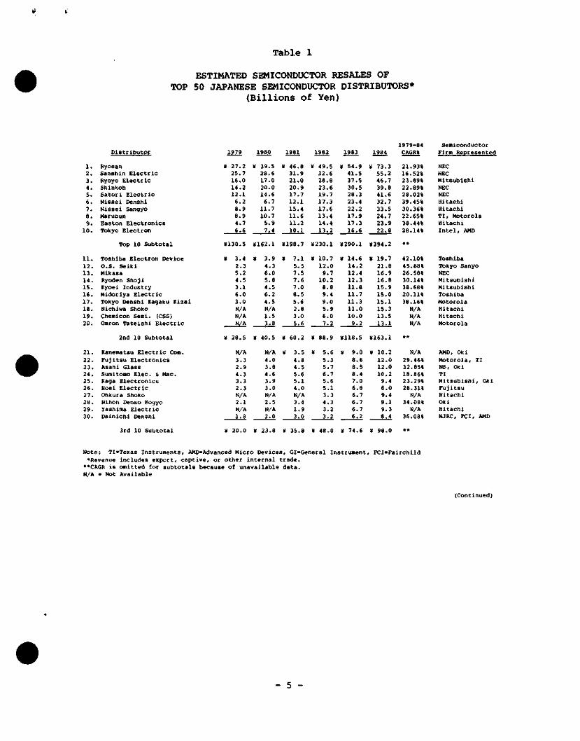
Table 1
ESTIMATED SEMICONDUCTOR RESALES OF TOP 50 JAPANESE SEMICONDUCTOR DISTRIBUTORS*
(Bil l ions of Yen)
1. 2. 3. 4. 5.
«. 7. 8. 9. 10.
Distributor
Ryosan Sanshin Electric Byoyo Electric 5hin)(Oh Satori Electric Nissei Denshi Nissei Sangyo Marubun Easton Electronics ToItyo Electron
Top 10 Subtotal
11. Toshiba Electron Device 12. O.S. Seilti 13. Miltasa 1 4 . Ryoden Shoji 15. Kyoei Industry 16. Hidorlya Electric 1 7 . Toltyo Denshi Kagaku Kizal 1 8 . Nlchiwa Shoko 19. Chemicon Semi. (CSS) 20. Omron Tatelshi Electric
1979
H 2 7 . 2 25.7 16.0 14.2 12.1 6.2 8.9 8.9 4.7 6.6
11130.5
V 3.4 2.3 5.2 4.5 3.1 6.0 3.0 N/A N/A N/A
1980
y 39.5 28.6 17 .0 20.0 14.6 6.7 11.7 10.7 5.9 7.4
11162.1
V 3.9 4.3 6.0 5.8 4.5 6.2 4.5 N/A 1.5 3.8
1981
V 46.8 31.9 21.0 20.9 17.7 12.1 15.4 11.6 11.2 10.1
V198.7
¥ 7.1 5.5 7.5 7.6 7.0 8.5 5.6 2.8 3.0 5.6
1982
V 49.5 32.6 28.8 23.6 19.7 17.3 17.6 13.4 14.4 13.2
11230.1
< 10.7 12.0 9.7 10.2 8.8 9.4 9.0 5.9 6.0 7.2
1983
V 5 4 . 9 41.5 37.5 30.5 28.3 23.4 22.2 17.9 17.3 16.6
V290.1
V 14.6 14.2 12.4 12.3 1 1 . 8 11.7 11.3 11.0 10.0 9.2
1984
V 73.3 55.2 46.7 39.8 41.6 32.7 33.5 24.7 23.9 22.8
11394.2
V 19.7 21.8 16.9 16.8 15.9 15.0 15.1 15.3 13.5 13.1
1979-84 CAGR%
21.93% 1 6 . 5 2 % 2 3 . 8 9 % 22.89% 28.02% 39 .45% 30 .36% 2 2 . 6 5 % 38 .44% 28 .14%
*•
42.10% 45.88% 26.58% 30.14% 38.68% 20.11% 38.16% N/A N/A N/A
Semiconductor Firm Represented
NEC NEC Mitsubishi NEC NEC Hitachi Hitachi TI, Motorola Hitachi Intel, AMD
Toshiba Toliyo Sanyo NEC Mitsubishi Mitsubishi Toshiba Motorola Hitachi Hitachi Motorola
2nd 10 Subtotal II 28.5 V 40.5 V 60.2 V 88.9 VllS.S V163.1
21. Kanematsu Electric Com. 22. Fujitsu Electronics 23. Asahi Glass 24. Sumitomo Elec. & Mac. 25. Kaga Electronics 26. Hoel Electric 27. Ohkura Shoko 2B. Nlhon Denso K09yo 29. Kashima Electric 30. Dainlchi Denshi
N/A 3.3 2.9 4.3 3.3 2.3 N/A 2 . 1 N/A 1 . 8
N/A V 3 .5 » 4 . 0 3 . 8 4 . 6 3 . 9 3.0 N/A 2.5 N/A 2.0
4.8 4.5 5.6 5.1 4 . 0 N/A 3 . 4 1 . 9 3 . 0
1 5 . 6 V 9 . 0 5.3 5.7 6 . 7 5 . 6 5 . 1 3 . 3 4 . 3 3 . 2 3 . 2
8.6 8.5 8.4 7.0 6.6 6.7 6.7 6.7 6.2
¥ 10.2 12.0 12.0 10.2 9.4 8.0 9.4 9.1 9.3 8 . 4
N/A 29 .46% 32.85% 18.86% 23 .29% 2 8 . 3 1 % N/A
3 4 . 0 8 % N/A
36.08%
AMD, Okl Motorola, TI NS, Oki TI Mitsubishi, Oki Fujitsu Hitachi Oki Hitachi NJRC, FCI, AMD
3rd 10 Subtotal ¥ 20.0 ¥ 23.8 ¥ 35 .8 ¥ 48.0 ¥ 74.6 ¥ 98.0
Note: TI=Texas Instruments, AMD=Advanced Micro Devices, GI'General Instrument, FCI-Falrchild •Revenue includes export, captive, or other internal t rade . **CAGR is omitted for subtotals because of unavailable da ta . N/A ' Not Available
(Continued)
- 5 -
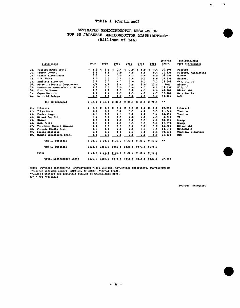
Table 1 (Continued)
ESTIMATED SEMICONDUCTOR RESALES OF TOP 50 JAPANESE SEMICONDUCTOR DISTRIBUTORS*
(Billions of Yen)
31. 32. 33. 3 4 . 3 5 . 3 6 . 3 7 . 3 8 . 3 9 . 40.
Distributor
Fujitsu Buhin Shoji Kantoh Denshi Tohman Electronics T .v . Sholiai Ashitate Electric Hitachi Electric Compone Kanematsu Semiconductor Koshida Sholtoh Japan Macnics
Dainichi Seigyo
!nts Sales
1979
V 1 . 5 1.6 2.2 1 . 5 3 . 1 N/A 1 . 8 1 . 0 1 . 1 1 . 8
1980
K 1 . 9 1.8 2.6 2.3 3.7 N/A 2.3 1 . 2 1 . 4 2.2
1981
V 2.4 2 . 9 3 . 5 3 . 6 4 . 7 1 . 4 2 . 9 1 . 9 1 . 9 2.6
1982
V 2.9 4.0 4.2 S.O 5.0 3.0 3.6 3.0 2.3 3.0
1983
V 5.9 5.8 5.6 5.5 5.2 5.0 4.7 4.3 4.2 4.2
1984
« 7 . 4 8.4 8.9 5.0 7.2
11.0 6.1 6.0 4.7 5.6
1979-84 CAGRt
37.60%
39.33* 32.25*
27.23* 18.36* N/A
27.65* 43.10* 3 3 . 7 0 * 2 5 . 4 8 *
Semiconductor
Firm Represented
Fujitsu
Fujitsu, Matsushita Mosteic
Hitachi OI(i, TI, GI
Hitachi PCI, GI Mitsubishi OI(i, Harris AMD
4th 10 Subtotal • 15.6 V 19.4 V 27.8 V 36.0 « 50.4 < 70.3
41. 42. 43. 44. 45. 4 6 . 4 7 . 4 6 . 4 9 . 5 0 .
Internix
Tokyo Shuna Kenden Kogyo Mitsui Co, L t d . Nideco
O.K. Denki Tachibana Shokal (Osaka) Chiyoda Denshi Kiki Sankoh Electric Numata Donyokusha Shoji
V 2 . 6 ¥ 2.9 V 3.1 < 3.8 ¥ 4.2 ¥ 7.1 2 . 1 1.8 3.4 1.6 1.8 1.7 1.5 0.8 1.3
2.6 2.2 3.8 2.2 2.2 2.3 1.9 1.2 1.7
3.2 2.8 6.S 2.7 2 . 7 3 . 0 2 . 4 1.5 2.1
3.5 3.1 4.8 3.1 3.3 3.4 2.7 2.0 2.4
4.1 4.1 4 . 0 3.7 3.7 3.6 3.4 3.1 3.0
5.5 5.4 4.3 4.0 5.0 S.O 4.5 4.4 4 . 0
22.25*
21.24* 24.57* 4.81*
20.11* 22.67*
24.08* 24.57* 40.63* 25.21*
Intersil
Toshiba
Toshiba TI Sharp Sharp
Mitsubishi Matsushita Toshiba, Signetics NEC
5th 10 Subtotal
Top 50 Subtotal
Total Distributor Sales
V 18.6 ¥ 23.0 ¥ 30.0 ¥ 32.1 ¥ 36.9 ¥ 49.2 •*
¥213.2 ¥268.8 ¥3S2.5 ¥435.1 ¥570 .5 ¥774.8
¥ 13.7 ¥ 1 8 . 4 ¥ 25.9 ¥ 3 1 . 3 ¥ 44.0 ¥ 48.3
¥226.9 ¥287.2 ¥378.4 ¥466.4 ¥614.5 ¥823.1 29.40*
Note: TI^Texas Instruments, AMD=Advanced Micro I3evices, GI-General Instrument, FCI-Fairchild
•Revenue includes export, captive, or other internal t r a d e . **CAGR is omitted for subtotals because of unavailable data. N/A > Not Available
Sou rce: DATAQUEST
- 6 -
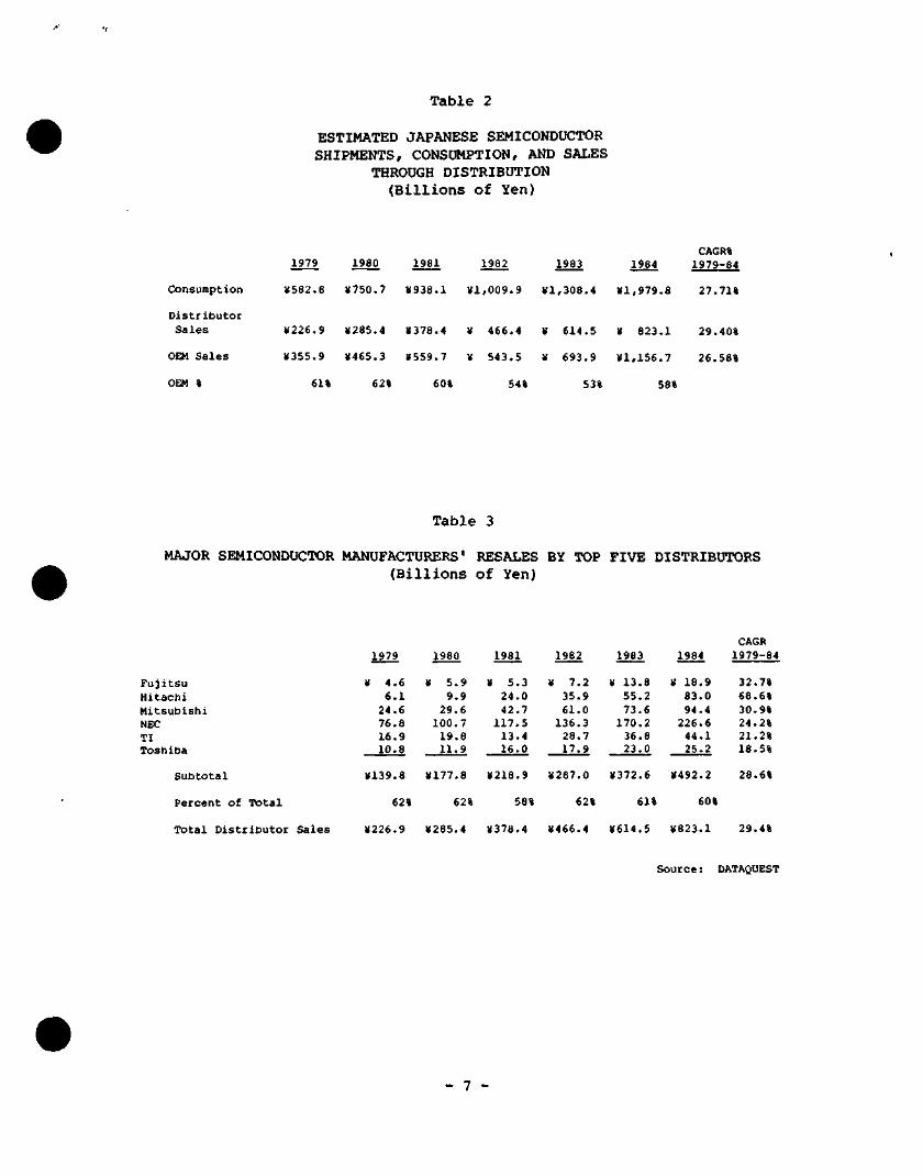
Table 2
ESTIMATED JAPANESE SEMICONDUCTOR SHIPMENTS, CONSUMPTION, AND SALES
THROUGH DISTRIBUTION (Billions of Yen)
Consumption
Distributor Sales
OEM Sales
OEM %
1979 1980 1981 1982 1983 1984
)i582.8 V750.7 11938.1 Vl,009.9 VI,308.4 VI,979.8
CAGR% 1979-84
27.71*
V226.9 V285.4 V378.4 V 466.4 V 614.5 V 823.1 29.40%
V355.9 ¥465.3 V559.7 V 543.5 V 693.9 ¥1,156.7 26.58%
61% 62% 60% 54% 53% 58%
Table 3
MAJOR SEMICONDUCTOR MANUFACTURERS' RESALES BY TOP FIVE DISTRIBUTORS (Billions of Yen)
Fujitsu Hitachi Mitsubishi NEC TI Toshiba
Subtotal
Percent of Total
Total Distributor Sales
1979
¥ 4.6 6.1 24.6 76.8 16.9 10.8
¥139.8
62%
¥226.9
1980
¥ 5.9 9.9
29.6 100.7 19.8 11.9
¥177.8
62%
¥285.4
1981
¥ 5.3 24.0 42.7
117.5 13.4 16.0
¥218.9
58%
¥378.4
1982
¥ 7.2 35.9 61.0
136.3 28.7 17.9
¥287.0
62%
¥466.4
1983
¥ 13.8 55.2 73.6
170.2 36.8 23.0
¥372.6
61%
¥614.5
1984
¥ 18.9 83.0 94.4 226.6 44.1 25.2
¥492.2
60%
¥823.1
CAGR 1979-84
32.7% 68.6% 30.9% 24.2% 21.2% 18.5%
28.6%
29.4%
Source: DATAQUEST
- 7 -
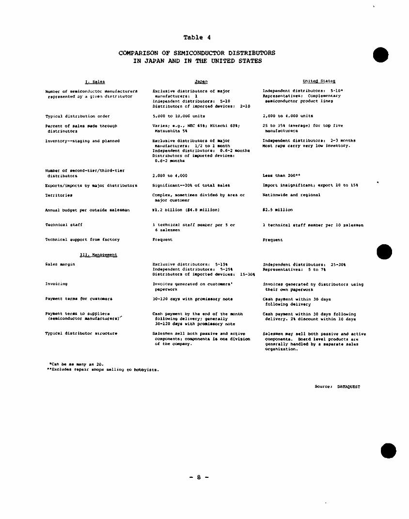
Table 4
COMPARISON OF SEMICONDUCTOR DISTRIBUTORS IN JAPAN AND IN THE UNITED STATES
I, Sales
Number of scniiconductor manufacturers represented by a givea distributor
Typical distribution order
Percent of sales made through distributors
Inventory—staging and planned
Number of second-tier/third-tier distributors
Exports/imports by major distributors
Territories
Annual budget per outside salesman
Japan
Exclusive distributors of major manufacturers: 1 Independent distributors: 5-10 Distributors of imported devices: 2-10
5,000 to 10,000 units
Varies; e.g., NEC 65%; Hitachi 60t; Matsushita 5%
Exclusive distributors of major manufacturers: 1/2 to 1 month Independent distributors: 0.6-2 months Distributors of imported devices: 0.6-2 months
2,000 to 4,000
Significant—20% of total sales
Complex, sometimes divided by area or major customer
Vl.2 billion ($4.8 million)
United States
Independent distributors: 5-10* Representatives: Complementary semiconductor product lines
2,000 to 4,000 units
25 to 35% (average) for top five manufacturers
Independent distributors: 2-3 months Most reps carry very low inventory.
Less than 200**
Import insignificant; export 10 to 15%
Nationwide and regional
$2.5 million
Technical staff
Technical support from factory
1 technical staff member per 5 or 6 salesmen
Frequent
1 technical staff member per 10 salesmen
Frequent
III. Management
Sales margin
Invoicing
Payment terms for customers
Payment terms to suppliers (semiconductor manufacturers)^
Typical distributor structure
Exclusive distributors: 5-15% Independent distributors: 5-25% Distributors of imported devices: 15-30%
Invoices generated on customers' paperwork
30-120 days with promissory note
Cash payment by the end of the month following delivery; generally 30-120 days with promissory note
Salesmen sell both passive and active components; components is one division of the company.
Independent distributors: 25-30% Representatives: 5 to 7%
Invoices generated by distributors using their own paperwork
Cash payment within 30 days following delivery
Cash payment within 30 days following delivery. 2% discount within 10 days
Salesmen may sell both passive and active components. Board level products are generally handled by a separate sales organization.
*Can be as many as 20. ••Excludes repair shops selling to hobbyists.
Source: DATAQUEST
- 8 -
Table 5
ESTIMATED AVERAGE MONTHLY SEMICONDUCTOR CONSUMPTION BY REGION 1983 AND 1984
(Billions of Yen)
1983 1984 Rank
1 2 3 4 5 6 7
Region
Kan to Kinki Tokai Shinetsu Shikoku Tohoku Chugoku
Others
Total
Consumption
H 58.6 15.8 14.6 7.9 3.8 3.4 2.7
2.2
X109.0
TAM*
¥41.3 11.4 11.1 4.5 3.1 2.5 1.9
1.0
¥76.8
Consumption
¥ 85.3 24.7 19.9 13.6 4.5 8.1 4.6
4.3
¥165.0
TAM*
¥ 66.9 21.0 16.8 9.6 3.7 6.6 3.4
2.3
¥130.3
Note: Others include Hokkaido, Hokuriku, and Kyushu. *Total Available Market excluding captive consumption
Sou r c e: DATAQUEST
- 9 -
Table 6
ESTIMATED AVERAGE MONTHLY SEMICONDUCTOR CONSUMPTION pY PREFECTURE 1983 AND 1984
(Billions of Yen)
1983 1984 Rank Region
1 2 3 4 5 6 7 8 9 10
Kanagawa Tokyo Osaka Tochigi Aichi Nagano Ibaraki Shizuoka Saitama Ehime
Top 10 others
Total
Consumption
¥ 23.2 13.6 7.0 6.5 6.0 5.7 5.4 5.3 4.7 3.4
80.8 28.2
¥109.O
TAM*
¥17.7 8.9 5.0 3.8 4.6 3.4 4.5 4.0 3.7 2.9
58.5 18.3
¥76.8
Consumption
¥ 34.6 21.9 10.3 11.0 9.
10, 7. 8. 8. 4.0
125.9 39.1
¥165.0
TAM*
I 25.9 14.4 8.0 6.7 6.5 7. 6. 6. 6. 3.
.1
.3 ,9 .7 ,3
91.8 38.5
¥130.3
*Total Available Market excluding captive consumption
Source: DATAQUEST
- 10 -
Table 7
ESTIMATED AVERAGE MONTHLY SEMICONDUCTOR CONSUMPTION AND TAM FOR VCRS
1983 AND 1984 (Billions of Yen)
1983 1984 Rank
1 2 3 4 5 6 7 8 9 10
Region
Kanagawa Ibaragi Ehime Osaka Tochigi Aichi Okayama Gumma Chiba Kyoto
Top 10 Others
Consumption
s 3.1 1.8 1.8 1.8 1.6 1.5 0.9 0.8 0.4 0.3
14.0 1.2
TAM*
V 3.0 1.5 1.6 1.7 1.0 1.3 0.8 0.6 . 0.3 0.3
12.1 0.7
Consumption
¥ 3.9 1.9 1.8 2.0 2.3 1.8 1.3 1.5 0.4 0.8
17.7 3.6
TAM*
¥ 3.8 1.5 1.5 1.8 0.9 1.6 1.1 1.2 0.4 0.7
14.6 3.6
Total ¥15.2 ¥12.8 ¥21.3
*Total Available Market excluding captive consumption
¥ 1 8 . 2
S o u r c e : DATAQUEST
- 11 -
Table 8
ESTIMATED AVERAGE MONTHLY SEMICONDUCTOR CONSUMPTION FOR COMPUTERS AND TERMINALS
1983 AND 1984 (Billions of Yen)
1983 1984 Rank
1 2 3 4 5
Reg ion
Tokyo Kanagawa Nagano Nara Yamanashi
Top 5 Others
Consumption
¥ 4.6 2.6 2.1 1.6 1.2
12.1 6.3
TAM*
X 2.7 2.0 1.0 1.4 1.1
8.2 3.7
Consumption
¥ 7.3 5.1 3.7 2.0 1.3
19.4 11.8
TAM*
¥ 4.5 3.2 2.1 1.7 1.2
12.7 7.7
Total ¥18.4 ¥11.9 ¥31.2 ¥20.4
*Total Available Market excluding captive consumption
Source: DATAQUEST
- 12 -
JAPANESE RESEARCH NEWSLETTER
JSIA Code: Newsletters
JAPAN TAKES CENTER STAGE AT ISSCC 1985
SUMMARY
Japan's "take-lead" strategy in semiconductor research is beginning to pay off. Of the 108 technical papers introduced at the 1985 International Solid State Circuits Conference (ISSCC), Japanese research teams presented 49 papers, or 44 percent, in contrast with 41 papers for the United States, 13 for Europe, and 5 for Canada. As shown in Figure 1, the number of Japanese papers presented at the conference has doubled since 1980, reflecting the heavy R&D investment made by Japanese companies. Hitachi was the leader, with 14 papers, followed by Toshiba and NEC, as shown in Table 1. Japanese research closely mirrors the commercial market: 40 percent of all the Japanese papers concentrated on memory technology, 26 percent on video consumer applications, and 16 percent on gate arrays. Clearly, the highlight of the 1985 ISSCC was the profusion of 1Mb DRAMs, 256K CMOS SRAMs, and nonvolatile memories. But DATAQUEST observes that Japanese makers are also dominant players in CMOS and GaAs gate arrays and image-sensing technology.
HIGHLIGHTS OF THE ISSCC
1Mb DRAMs
East-West competition is heating up in 1Mb DRAMs, an area dominated by the Japanese in 1984. AT&T and Mostek presented CMOS devices using 1.2- to 1.3-micron geometries, while IBM offered a fast-page-operation NMOS device with 1.5-micron line widths. As shown in Table 2, Japanese 1Mb DRAMs generally use finer geometries (l.O to 1.2 microns), smaller cell sizes (20 to 35 ^ ) , and smaller die sizes (43 to 65 mm^) . Three Japanese companies offer NMOS designs (Mitsubishi, NEC, and Toshiba); two companies offer CMOS prototypes , (Hitachi and Toshiba). Many of the devices use planar, double-poly, one-transistor cells.
© 1985 Dataquest Incorporated March 18 ed.-Reproduction Prohibited
The content o( this report represents our interpretaion and anaIysis of information generally available to the public or released by fosponsible individuals in the subject companies, but ts not guaranteed as to accuracy or completeness It does not contain material provided to us in confidence by our clients Individual companies reponed on and analyzed by DATAQUEST, may be clients of this and/or other DATAQUEST services This information is not furnished in connection with a sale or offer to sell securities or in connection with the solicitation of an offer to buy securities This firm and its parent and/or their officers, stockholders, or members of their families may, from time to time, have a long or short position in the securities mentioned and may sell or buy such securities
Azabu Heights, Suite 711, 1-5-10 Roppongi, MInato-ku, Tokyo 106, Japan 1290 Bidder Park Drive / San Jose, CA 95131 / (408) 971-9000 / Telex 171973
The 1Mb DRAMS offer a variety of new features. NEC's quasi 4-bit-wide test circuit and Mitsubishi's raultibit test mode reduce testing time. Toshiba's device features a folded capacitor cell structure using its buried oxide (BOX) isolation technology. Toshiba and IBM both offer fast-page-operation modes. Hitachi's CMOS device has an address transition detection feature to reduce power dissipation at long cycle times and a back bias generator to reduce standby power dissipation.
New memory cell structures that may be used in 4Mb DRAMs also made their appearance. Hitachi introduced a 4b {16-level) cell storage for use in a semiconductor file memory. The 4Kb test circuit can read and write a multilevel signal in a cell without using complicated precision circuits. Fujitsu introduced a 1Mb DRAM with three-dimensional stacked capacitor cells (word line, storage node, and cell plate). These technologies are the early results of MITI's New Semiconductor Function Elements Project, which is investigating three-dimensional ICs.
Nonvolatile Memories
Japanese companies are focusing heavily on EPROM technology because of its ease of programming and low process costs. Hitachi's 1Mb CMOS EPROM offers fast-page-mode programming comparable to the time required to program a 256K EPROM. Toshiba's asynchronous 1Mb CMOS EPROM offers an address transistor detector, a mid-word-line buffer, and sensing to achieve an BOns access time. Hitachi also presented a 256K CMOS EPROM that avoids latch-up problems by using polysilicon PMOS FETs in the programming control circuit. Toshiba's 256K flash EEPROM overcomes the problems of conventional UV-EPROMs and EEPROMs by rejecting failed devices with a burn-in test after plastic packaging. DATAQUEST notes that in 1986 Toshiba plans to commercialize 64K flash EEPROMS for which it has developed low-cost production techniques.
SRAMs
Japanese makers dominated this session with their 256K CMOS SRAMs. Hitachi's 32Kx8b device features variable impedance loads and a pulsed word-line technique to attain fast access times and low power dissipation during the write cycle (see Table 3). NEC uses a buried isolation structure and three-layer configuration to achieve a small die size. Its 256K CMOS SRAM consumes only lOmW standby power because doping of the polysilicon layer has been optimized. Mitsubishi's device offers a tri-level word line to minimize the peak current and a data equalizing technique to achieve high-speed operation.
Other papers introduced included Toshiba's paper on a 64K CMOS SRAM with a Schmitt trigger sense amplifier. Motorola's paper on a 16K SRAM, and NEC's paper on a CML-compatible GaAs 4K SRAM (see Table 4).
- 2 -
Flexible Gate Arrays
Despite predictions of their imminent decline, gate arrays are still popular among Japanese manufacturers because of their shorter fab cycle, fewer masks, and improved CAD systems. In addition, new array architectures offer more flexibility. Toshiba's 24,000-gate CMOS array offers triple-level wiring and a hierarchical layout that allows tighter designs. Fujitsu's 240,000-transistor CMOS masterslice features a flexible allocation of memory and channels to increase the memory area. Mitsubishi Electric presented a CMOS gate array with configurable 1,024b ROM and 256b RAM using a 1.5-micron design rule. Hitachi's 4,000-gate CMOS array has automatically generated test circuits to reduce testing time, a process that is becoming increasingly time consuming with larger arrays.
High-Speed Gate Arrays
Besides flexible gate arrays, Japanese makers are focusing on high-speed gate arrays using bipolar, GaAs, and CMOS technologies. Nippon Telegraph and Telephone (NTT) presented an BOps 2,500-gate bipolar macrocell array with ECL compatibility, using a 1.0-micron rule super self-aligned process technology (SST), to make a 26b parallel multiplier. Oki's 390ps 1,000-gate array uses GaAs MESFET superbuffer FET logic and offers high load drivability and low power dissipation. Toshiba's 42ps 2,000-gate GaAs gate array offers a small gate delay and low power consumption, making it an attractive alternative to ECL gate arrays. DATAQUEST observes that Japanese manufacturers are seeking faster development times because of shortening product life cycles in Japan's competitive market.
Image Sensors
Japan's video camera market is also pushing development of charge-coupled device (CCD) image sensors. Matsushita introduced two papers, one covering a 490 x 490-element super-8 format CCD color imager using a vertical overflow drain for blooming supression and wider dynamic range, and one about a collinear contact-type three-chip CCD image sensor containing a plane structure of photosites. Sharp presented a 580 X 500-element interline-transfer CCD imager for the 2/3-inch format that offers a high-aperture ratio and a low smear level. Mitsubishi's 480 X 400-element CCD imager features a charge sweep device that allows narrower vertical channel widths without a decline of the charge-handling capacity.
Sheridan Tatsuno
- 3 -
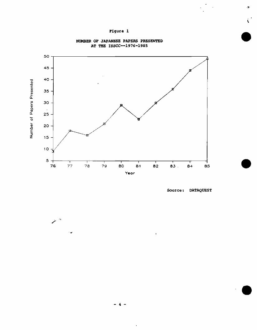
Figure 1
NUMBER OF JAPANESE PAPERS PRESENTED AT THE ISSCC—1976-1985
T3 V
-t-r c <u en lU
o a. D
Q.
t) .O
E 3
S3 . 84 85
Year
Source ; DATAQUEST
^
- 4 -
Table 1
NUMBER OF JAPANESE PAPERS PRESENTED AT THE ISSCC BY ORGANIZATION—1976-1985
Private Firms
NEC Hitachi Toshiba Fujitsu Sharp Matsushita Mitsubishi Sanyo Oki Sony TI Japan
Government Agencies
Nippon Telegraph 6 Telephone (NTT)
VLSI Development Laboratory
MITI Electronic Technology Laboratory
Control Research Laboratory
Tohuku University
Total
1976
1 1 4 1 -2 -----9
—
• • •
-
*F'
-0
9
1977
3 1 3 2
--1 ----10
3
1
1
2
1 8
18
1978
4 3 1 1 1 -1 1
-1
-13
3
-
-
-
-3
16
1979
4 5 1 --2 1 -1 --14
6
1
-
-
-7
21
1980
5 6 3 4 -3 1 --1
-23
4
1
—
-
1 6
29
1981
4 6 2 2 1 -1 -1 4 -21
2
-
-
-
-2
23
1982
6 4 5 3 1 1 2 --1 -23
7
-
-
-
-7
30
1983
7 3 4 11 1 2 3 --2 -33
3
-
-
-
-3
36
1984
6 8
11 4 -4 1 -2 3 1 40
4
-
-
-
-4
44
1985
8 14 9 4 1 3 4 -1 2 -46
2
— •
-
-
1 3
49
Total
48 51 43 32 5
17 15 1 5
14 1
232
34
3
1
2
3 43
275
Source: DATAQUEST
- 5 -
Table 2
SPECIFICATIONS OF 1Mb DRAMS
Company
NEC
Mitsubishi
Toshiba
Fujitsu
Toshiba
Hitachi
ATtT
Mostek
IBM
Die Size (mm^)
4.6 X 9.4 (43.24)
5.0 X 13.0 (65.00)
4.78 X 13.23 (63.24)
4.45 X 12.3 (54.74)
5.0 X 12.5 (62.50)
4.68 X 10.1 (47.27)
4.8 X 14.5 (69.60)
6.0 X 11.4 (68.4)
5.5 X 10.5 (57.75)
Cell Size ( fm^)
3.4 X 6.0 (20.40)
3.8 X 9.4 (35.72)
5.0 X 6.4 (32.00)
3.15 X 8.4 (26.46)
3.8 X 9.0 (34.20)
3.35 X 7.2 (24.12)
3.5 X 10.5 (36.75)
4.0 X 9.0 (36.00)
4.1 X 8.8 (36.08)
Design ( ra)
1.5
1.2
1.2
1.4
1.2
1.5
1.3
1.2
1.5
Process
^•K>s
NMOS
NMOS
NMOS
CMOS
CMOS
CMOS
CMOS
NMOS
Access Time (ns)
85
90
70
90
56
74
80
N/A
80
Functions Available
Quasi 4-bit-wlde testing
Multibit test mode Shared sensing
Folded capacitor cell structure Buried oxide (BOX) isolation
Three-dimensional stacked capacitor cells
Fast page and static column modes Substrate bias generator Laser redundancy
Address transition detection Back bias generator
On-chip substrate bias generator
Divided bit-line matrix architecture
Fast page operation
N/A > Not Available
Table 3
SPECIFICATIONS OF JAPANESE 256K CMOS SRAMs
Company
Hitachi
NEC
Matsushita
Die Size (mm^)
4.98 x 9.16 (45.62)
5.09 X 8.00 (40.72)
5.41 X 9.18 (49.66)
Cell Size (nm^)
N/A (94.72)
7.4 X 12.1 (89.54)
8.0 X 14.5 (116.0)
Design (Mm)
1.2
1.2
1.3
Process
Hl-CMOS
CMOS
CMOS
Access Time (ns)
45
55
45
Functions Available
Variable impedance loads Pulsed Hord-line Address transition detection
lOuW standby power Buried isolation Ti polycide gate
Trilevel word line Address transition activated circuit
N/A - Not Available
Source: ISSCC Proceedings DATAQUEST
- 6 -
^
Table 4
TOPICS OF JAPANESE PAPERS PRESENTED AT THE 1985 ISSCC
Company
1Mb DRAMs
NEC
Mitsubishi
Toshiba
Hitachi
Fujitsu
Toshiba
Hitachi
Title of Paper
85ns 1Mb DRAM in a 300-mil Plastic DIP with Quasi 4-bit-Wide Testing and Double Level Polycide
90ns NMOS 1Mb DRAM with Multi-bit Test Mode and Shared Sensing Scheme
1Mb NMOS DRAM with a Folded Capacitor Cell Structure, Using Buried Oxide (BOX) Isolation and Two-Level Aluminum Metal
16-Levels/Cell Storage, Single Transistor DRAM for Use in Semiconductor File Memory
1Mb DRAM with 3-Dimensional Stacked Capacitor Cells and 55fG Capacitance
1Mb CMOS DRAM with 24ns Column and 56ns Row Access Times, Using Bit-Line Precharge with Complementary Capacitor Coupled Dummy Cell and Bit-Line Level Generator
20ns Static Column 1Mb CMOS DRAM, Using Back Bias Generator and Corrugated Capacitor Cell (CCC)
Nonvolatile Memory
Hitachi
Toshiba
Hitachi
Toshiba
95ns 256K CMOS EPROM, Using Polysilicon PMOS FETs in the Programming Control Circuit
256K Flash EEPROM Using Triple Polysilicon and 2.0 Micron Design Rule
1Mb CMOS EPROM with Fast Page Mode Programming, Using High-Voltage MOS Structure with Lightly Doped Drain, Double Poly N-Well CMOS, and 1.0 Micron Minimum Gate Length
Programmable BOns 1Mb CMOS EPROM with Address Transition Detector and Mid-Word-Line Buffer, Using Selective Diffused Self-Alignment (DSA)
(Continued)
- 7 -
Table 4 (Continued)
TOPICS OF JAPANESE PAPERS PRESENTED AT THE 1985 ISSCC
f
Company
SRAMs
Hitachi
NEC
Mitsubishi
Toshiba
NEC
Title of Paper
256K CMOS SRAM with Variable Impedance Loads and Pulsed Word-Line Technique
lOmW Standby Power 55ns 256K CMOS SRAM Using 1.2 Micron P-Well CMOS, Ti Polycide Gate and Buried Isolation
45ns 256K CMOS SRAM with Tri-Level Word Line Using Double Poly Single Aluminum CMOS
17ns 64K CMOS SRAM with a Schmitt Trigger Sense Amplifier, Using Two-Level Aluminum Metal and Twin-Well CMOS Process
CML GaAs 4K SRAM with Source Coupled FET Logic for Peripheral Circuits and Conventional E/D-DCFL Circuitry for the Memory Cell
Special-Application Memories
NEC 256K Dual Port Memory
Matsushita
Fujitsu
8K Content-Addressable and Reentrant Memory, Using a Small Associative Memory Cell and PLA
64K ECL RAM with Two-Array Redundancy, Using 1.2-Microa Lithography and Isolation by Oxide and Polysilicon
Gate Arrays
Toshiba
Fujitsu
Mitsubishi
Hitachi
24,000 Gate CMOS Array Using Triple-Level Wiring and Hierarchical Layout
240K Transistor CMOS Array with Flexible Allocation of Memory Channels
1.5-Micron CMOS Gate Array (16-bit MPU) with 1,024b ROM and 256b RAM
4K CMOS Gate Array with Automatically Generated Test Circuits
(Continued)
8 -
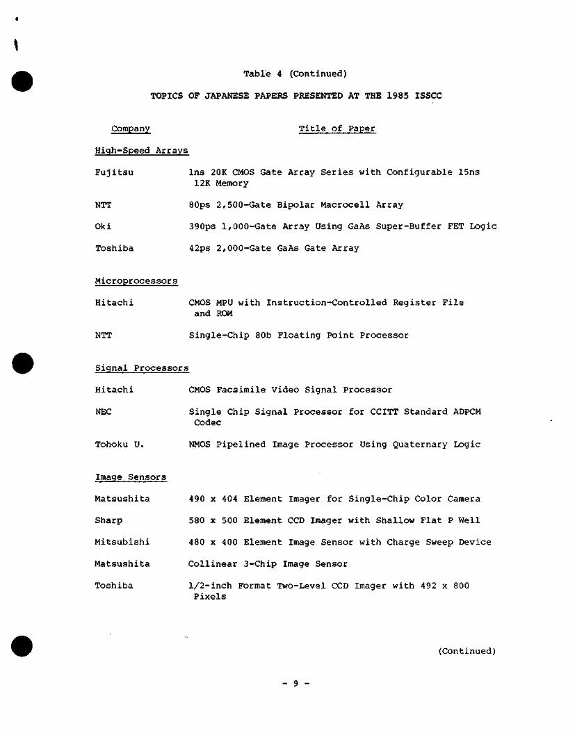
Table 4 (Continued)
TOPICS OF JAPANESE PAPERS PRESENTED AT THE 1985 ISSCC
Company
High-Speed Arrays
Fujitsu
Title of Paper
Ins 20K CMOS Gate Array Series with Configurable 15ns 12K Memory
NTT BOps 2,500-Gate Bipolar Macrocell Array
Oki 390ps 1,000-Gate Array Using GaAs Super-Buffer FET Logic
Toshiba 42ps 2,000-Gate GaAs Gate Array
Microprocessors
Hitachi
NTT
CMOS MPU with Instruction-Controlled Register File and ROM
Single-Chip 80b Floating Point Processor
Signal Processors
Hitachi CMOS Facsimile Video Signal Processor
NEC
Tohoku U.
Single Chip Signal Processor for CCITT Standard ADPCM Codec
NMOS Pipelined Image Processor Using Quaternary Logic
Image Sensors
Matsushita
Sharp
Mitsubishi
Matsushita
Toshiba
490 X 404 Element Imager for Single-Chip Color Camera
580 X 500 Element CCD Imager with Shallow Flat P Well
480 X 400 Element Image Sensor with Charge Sweep Device
Collinear 3-Chip Image Sensor
1/2-inch Format Two-Level CCD Imager with 492 x 800 Pixels
(Continued)
- 9 -
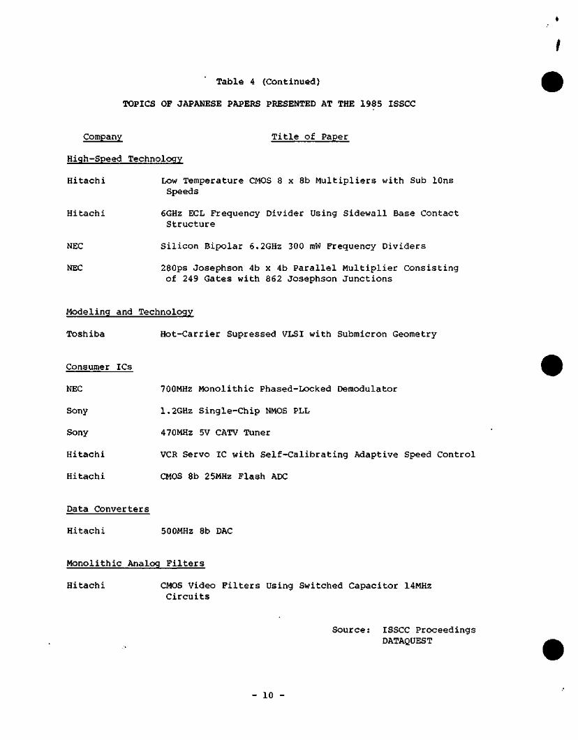
Table 4 (Continued)
TOPICS OF JAPANESE PAPERS PRESENTED AT THE 1985 ISSCC
Company Title of Paper
High-Speed Technology
Hitachi Low Temperature CMOS 8 x 8b Multipliers with Sub lOns Speeds
Hitachi 6GHz ECL Frequency Divider Using Sidewall Base Contact Structure
NEC Silicon Bipolar 6.2GH2 300 mW Frequency Dividers
NEC 280ps Josephson 4b x 4b Parallel Multiplier Consisting of 249 Gates with 862 Josephson Junctions
Modeling and Technology
Toshiba Hot-Carrier Supressed VLSI with Submicron Geometry
Consumer ICs
NEC 700MHz Monolithic Phased-Locked Demodulator
Sony 1.2GHz Single-Chip NMOS PLL
Sony 470MHz 5V CATV Tuner
Hitachi VCR Servo IC with Self-Calibrating Adaptive Speed Control
Hitachi CMOS 8b 25MHz Flash ADC
Data Converters
Hitachi 500MHz 8b DAC
Monolithic Analog Filters
Hitachi CMOS Video Filters Using Switched Capacitor 14MHz Circuits
Source: ISSCC Proceedings DATAQUEST
- 10
Dataquest JAPANESE RESEARCH NEWSLETTER
JSIA Code: Newsletters
JAPANESE SEMICONDUCTOR ACTIVITY IN THE UNITED STATES—1984 UPDATE
SUMMARY
Japanese semiconductors are becoming an increasingly pervasive part of the U.S. semiconductor market. The 1984 events contributing to this include the following:
• Imports of Japanese semiconductors into the United States continued at record high levels. Finished goods imports were up 123 percent in 1984 over 1983.
• Total 1984 Japanese company semiconductor sales grew much faster than those of U.S. companies.
• A seventh Japanese firm established manufacturing facilities in the United States.
• U.S. semiconductor sales by Japanese companies grew 83 percent from 1983 to 1984.
• The Japanese share of the U.S. semiconductor market jumped from 13.9 percent to 17.4 percent in 1984.
U.S.-JAPAN SEMICONDUCTOR TRADE
Table 1 shows U.S.-Japan semiconductor trade from January through September of 1984 compared with the same period in 1983. The numbers in this table represent DATAQUEST estimates of the total market value of imports plus locally manufactured product (e.g., devices assembled by Fujitsu in the United States for sale in the United States). While sales by Japanese companies increased more than 120 percent January through September year-to-date, growth was most dramatic in MOS logic. This is due in part to a huge influx of microprocessor products imported from Japan to the United States.
© 1985 Dataquest Incorporated Feb. 26 ed.-Reproduction Prohibited
The content of this report represents our interpretaion and analysis of information generally available to the public or released by responsible individuals in the subject companies, but is not guaranteed as to accuracy or completeness. It does not contain material provided to us in confidence by our clients Individual companies reported on and analyzed by DATAQUEST. may be clients of this and/or other DATAQUEST services This information is not furnished in connection with a sale or offer to sell securities or in connection with the solicitation of an offer to buy securities This firm and its parent and/or their officers, stockholders, or nnembers of their families may, from time to time, have a long or short position in the securities mentioned and may sell or buy such securities
Azabu Heights, Suite 711, 1-5-10 Roppongi, Minato-ku, Tokyo 106, Japan 1290 Ridder Park Drive / San Jose, CA 95131 / (408) 971-9000 / Telex 171973
PRELIMINARY 1984 MARKET SHARE DATA
Preliminary 1984 market share data show that on the average, total semiconductor sales of major U.S. companies grew approximately 46 percent over 1983, exhibiting an average compound annual growth rate (CAGR) of 15 percent from 1980 to 1984. Total semiconductor sales of major Japanese companies grew an average of 58 percent in 1984, with an average CAGR of 34 percent from 1980 to 1984. This is shown in Table 2. For the purposes of this analysis, we define "major company" as any company for which DATAQUEST has published market share estimates for a given year. According to this definition, in 1980 there were 45 major U.S. companies and 7 major Japanese companies. In 1984, there were 55 major U.S. companies and 9 major Japanese companies.
Clearly, overall Japanese growth has been much higher than overall U.S. growth. The Japanese companies have fueled their growth with sustained capacity expansion, high levels of automation, a highly captive market for consumer and industrial electronic products, and a much-publicized export boom. The Japanese government-sponsored VLSI program, which ended in 1979 and led to Japanese development of the 64K DRAM, can be thought of as the catalyst for the dramatic growth in Japanese sales that has since occurred.
JAPANESE PRODUCTION FACILITIES IN THE UNITED STATES
With the addition of two more Japanese companies to the U.S. manufacturing base in 1984, the number of Japanese companies that manufacture semiconductors in the United States now stands at seven.
Oki Semiconductor opened its Sunnyvale, California, test facility in December 1984; assembly capability will be added in the summer of 1985. Mitsubishi Semiconductor America's Research Triangle Park, North Carolina, assembly and test plant is scheduled to open early in 1985. Hitachi is currently building a second assembly facility in Irving, Texas, which will also perform final metallization of gate arrays.
Toshiba Semiconductor USA (TSUSA) recently announced a plan to shut down its Sunnyvale plants due to the outmoded lines in place there; the company plans to build a new factory in the United States in 1987.
Fujitsu has announced plans to build a wafer fab in Oregon, to be completed in 1986. The major product will be 256K DRAMs.
Sharp and RCA recently announced a joint venture for designing, developing, and manufacturing CMOS VLSIs. Expectations are that this 49 percent Sharp-owned venture will build a factory in the United States in 1986.
NEC no longer fabricates wafers at the former Electronic Arrays plant in Mountain View, California. This facility is now used for assembly only.
>- 2 -
It should be noted that the presence of manufacturing facilities in the United States is a very effective way for Japanese companies to penetrate the U.S. market while at the same time soothing trade friction. U.S. plants are overseen, in general, by Japanese personnel, but most management personnel and staff are Americans. Products that are completely manufactured and sold in the United States are not included in import/export figures.
Most of the Japanese production in the United States is in MOS memories and logic; however, Matsushita assembles hybrid ICs. DATAQUEST estimates that the sales value of Japanese products fabricated and/or assembled in the United States was $350 million in 1984.
Table 3 shows Japanese manufacturing capability in the United States.
JAPANESE SALES IN THE UNITED STATES
Table 4 gives DATAQtJEST estimates of 1982, 1983, and 1984 total semiconductor sales in the United States by the nine major Japanese companies. We believe that sales by Japanese companies in the United States grew 83 percent to $2.1 billion in 1984. This represents 17.4 percent of the total 1984 U.S. semiconductor market. Hitachi is by far the leader with U.S. sales of $595 million, or 28.3 percent of total Japanese sales in the United States.
DATAQUEST believes that sales of Japanese company-manufactured semiconductors in the United States were up only 83 percent, while imports of finished goods increased 123 percent due to the following reasons:
Imports of raw wafers to be assembled United States increased only 74 percent.
and sold in the
• Between 10 percent and 15 percent of imported goods were not sold in 1984, and are currently in inventory.
Table 5 shows DATAQUEST estimates of the Japanese share of the U.S. semiconductor market from 1980 to 1984. Over that period, Japanese share gained 10.4 percentage points, to stand at 17.4 percent of the U.S. market in 1984. The largest part of this is in MOS ICs; the Japanese share of that market is now 27.2 percent. Figure 1 graphically illustrates the sharp rise in Japanese share of the U.S. market.
Patricia S. Cox
9 - 3 -
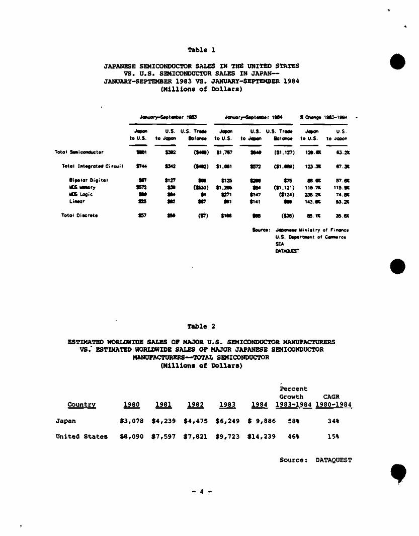
Table 1
JAPANESE SEMICONDUCTOR SALES IN THE UNITED STATES VS. U.S. SEMICONDUCTOR SALES IN JAPAN—
JANUARY-SEPTEMBER 1983 VS. JANUARY-SEPTEMBER 1984 (Millions of Dollars)
January-S»ptmb»r 19B3
U.S. U.S. Trodt
Jonuory-StptOTbtr 1904 X Chang* 1963-1964
Jopom U.S. U.S. Trod* Jopon U.S.
Totol Sskieenducter
Total Int«grat«d Circuit
Bipolar Digital MXUMory ICS Logic Linaor
Total Oiacroto
to U.S. to Japan
taei S302
$744 S342
iionca to U.S. to Japan Bol to U.S. to Japan
$67 $572 $Be
$25
$57
$127 $30 $84 $B2
$se
($408) $1,767
($402) $1,661
$66 $125 ($533) $1,205
$4 $271 $67 $61
$640
$572
($1,127) 120.ex
($1,009) 123.31
$200 $75 06.R $B4 ($1,121) 110.7X $147 ($124) 236.2X $141 $80 143.ex
($7) $106 ($36) 85. IX
63.2X
67.as
57.« 11S.9K 74.K 53.2(
35.ex
Seurco: Japonoso Miniitry of Tinonce U.S. Oapertnant of Comiiorce SIA OATAOUeST
Table 2
ESTIMATED WORLDWIDE SALES OF MAJOR U.S. SEMICONDUCTOR MANUFACTURERS VS.' ESTIMATED WORLDWIDE SALES OF MAJOR JAPANESE SEMICONDUCTOR
MANUFACTURERS—TOTAL SEMICONDUCTOR (Millions of Dollars)
Country
Japan
United States
1980 1981 1982 1983
Percent Growth CAGR
1984 1983-1984 1980-1984
$3,078 $4,239 $4,475 $6,249 $ 9,886 58% 34%
$8,090 $7,597 $7,821 $9,723 $14,239 46% 15%
Source: DATAQUEST
f - 4 -
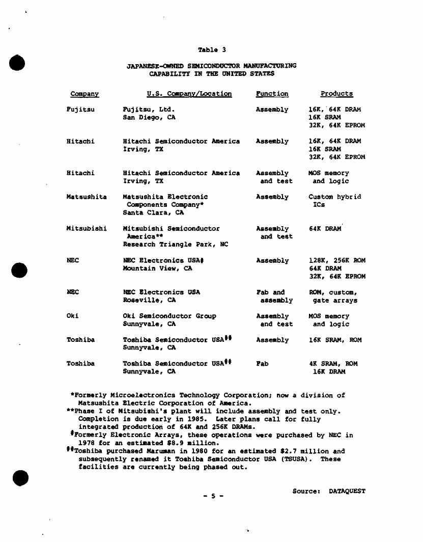
Table 3
JAPANESE-OWNED SEMICONDUCTOR MANUFACTURING CAPABILITY IN THE UNITED STATES
Company U.S. Company/Location Function
Fujitsu Fujitsu, Ltd. Assembly San Diego, CA
Hitachi Hitachi Semiconductor America Assembly Irving, TX
Hitachi Hitachi Semiconductor America Assembly Irving, TX and test
Matsushita Matsushita Electronic Assembly Components Company* Santa Clara, CA
Mitsubishi Mitsubishi Semiconductor Assembly America** and test Research Triangle Park, NC
NEC NEC Electronics USA# Assembly Mountain View, CA
NEC NEC Electronics USA Fab amd Roseville, CA assembly
Oki Oki Semiconductor Group Assembly Sunnyvale, CA and test
Toshiba Toshiba Semiconductor USA^^ Assembly Sunnyvale, CA
Toshiba Toshiba Semiconductor USA^^ Fab Sunnyvale, CA
Products
16K, 64K DRAM 16K SRAM 32K, 64K EPROM
16K, 64K DRAM 16K SRAM 32K, 64K EPROM
MOS memory and logic
Custom hybrid ICs
64K DRAM
128K, 256K ROM 64K DRAM 32K, 64K EPROM
ROM, custom, gate arrays
MOS memory and logic
16K SRAM, ROM
4K SRAM, ROM 16K DRAM
*Formerly Microelectronics Technology Corporation; now a division of Matsushita Electric Corporation of America.
**Phase I of Mitsubishi's plant will include assembly and test only. Completion is due early in 1985. Later plans call for fully integrated production of 64K and 256K DRAMs.
^Formerly Electronic Arrays, these operations were purchased by NEC in 1978 for eui estimated $8.9 million.
^^Toshiba purchased Maruiuan in 1980 for cin estimated $2.7 million and subsequently renamed it Toshiba Semiconductor USA (TSUSA). These facilities are currently being phased out.
- 5 -Source: DATAQUEST
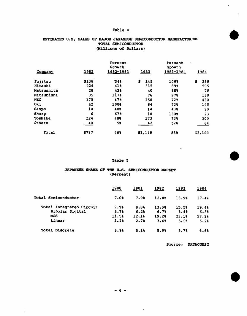
Table 4
ESTIMATED U.S. SALES OF MAJOR JAPANESE SEMICONDUCTOR MANUFACTURERS TOTAL SEMICONDUCTOR (Millions of Dollars)
Company
Fujitsu Hitachi Matsushita Mitsubishi NEC Oki Sanyo Sharp Toshiba Others
1982
$108 224 28 35 170 42 10 6
124 40
Percent Growth 1982-1983
34% 41% 43%
117% 47% 100% 40% 67% 40% 5%
1983
$ 145 315 40 76 250 84 14 10 173 42
Percent Growth 1983-1984
106% 89% 88% 97% 72% 73% 43% 130% 73% 52%
1984
$ 298 595 75 150 430 145 20 23 300 54
Total $787 46% $1,149 83% $2,100
Table 5
JAPANESE SHARE OF THE U.S. SEMICONDUCTOR MARKET (Percent)
1980 1981 1982 1983 1984
Total Semiconductor 7.0% 7 .9% 12.0% 13.9% 17.4%
Total Integrated Circuit Bipolar Digital MOS Linear
7.9% 3.7%
11.5% 3.2%
8.8% 6.2%
12.1% 2.7%
13.5% 6.7%
19.2% 3.4%
15.5% 5.4%
23.1% 3.2%
19.4% 6.3%
27.2% 5.2%
Total Discrete 3.9% 5 . 1 % 5 .9% 5.7% 6 .6%
Source : DATAQtreST
- 6 -
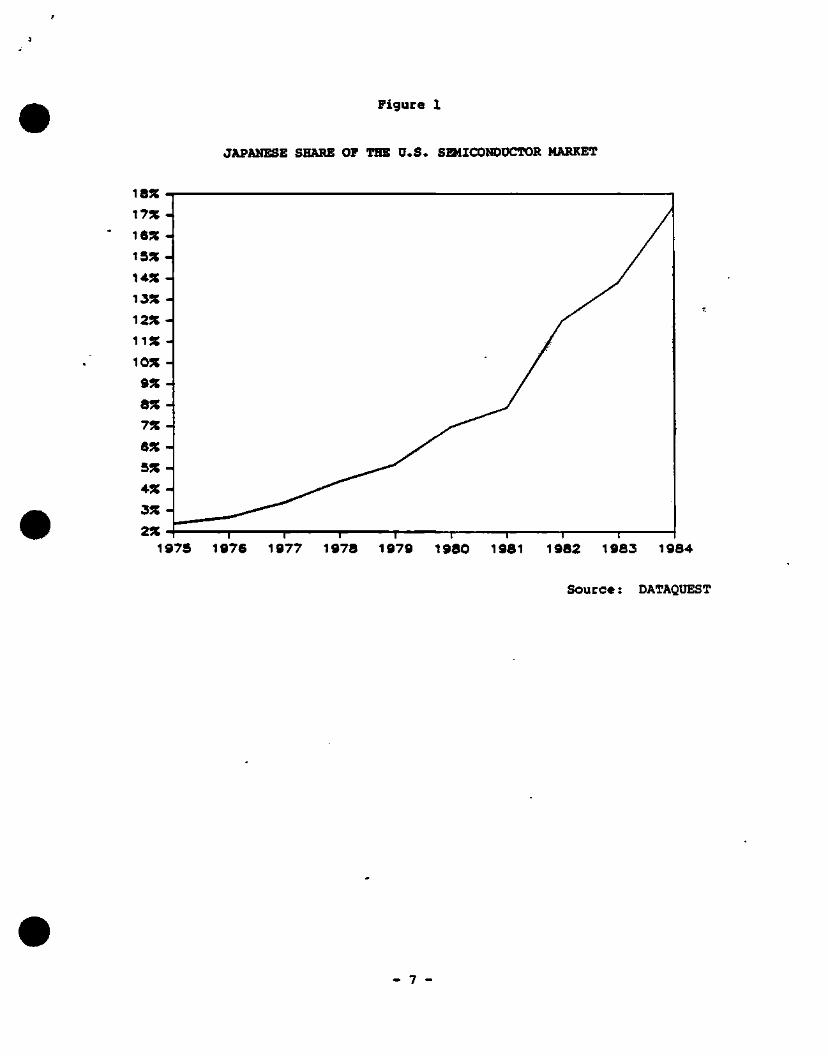
Figure 1
JAPANESE SHARE OF THE U . S . SEMICONDtTCTOR MARKET
1855 -r
1 9 7 5 1 9 7 6 1978 1979 — I 1980 1981
— I 1 1982 1983 1984
Source : DATAQUEST
- 7 -
JSIA Code: Newsletters
JAPANESE SEMICONDUCTOR TECHNOLOGY REVIEW FOURTH QUARTER 1984
SUMMARY
Japanese semiconductor makers finished 1984 with a profusion of new products and technologies, most of which were targeted for the Japan Electronics Show in October. During the fourth quarter, DATAQUEST recorded 112 major announcements—more than twice the 54 announcements made during the third quarter. The year was highlighted by the introduction of 1Mb DRAM and 256K SRAM prototypes, Nippon Telegraph and Telephone's 16K GaAs SRAM, and Hitachi's experimental 32-bit CMOS MPU. As shown in Figure 1, memory products and technologies led the way, but DATAQUEST also observes the following trends:
• New MPU/MCU product announcements exceeded those for advanced developments as top makers have kept quiet about their 16-bit and 32-bit MPU development activities.
• Japanese vendors are developing 15,000- to 20,000-gate arrays and standard cells, which are being used primarily in-house.
• The explosion of advanced research on optoelectronics and gallium arsenide (GaAs) is being driven by the introduction of laser-based compact disks, optical memory files, and optical communications.
• Linear/analog products are primarily driven by the VTR and telecommunication markets.
• Research on new semiconductor function ICs, including bio-sensors, 3-dimensional ICs, and superlattices, is being conducted at corporate and government labs.
Device technologies are being supported by a rush of new semiconductor equipment, which DATAQUEST believes is a result of the VLSI Project (1976-1980). Major semiconductor makers such as Hitachi, NEC, and Toshiba are developing advanced equipment for next-generation
© 1985 Dataquest Incorporated Jan. 23 ed.-Reproduction Prohibited
The content of this report represents our interpretaion and analysis of information generally availabie to the public or released by responsible individuals in the subject companies, but is not guaranteed as to accuracy or completeness. It does not contain material provided to us in confidence by our clients. Individual companies reported on and analyzed by DATAOUEST. may be clients of this and/or other DATAQUEST services This information is not furnished in connection with a sale or offer to sell securities or in connection with the solicitation of an offer to buy securities This firm and its parent and/or their officers, stockholders, or members of their families may, from time to time, have a long or short position in the securities mentioned and may sell or buy such securities
Azabu Heights, Suite 711, 1-5-10 Roppongi, Minato-ku, Tokyo 106, Japan 1290 Ridder Park Drive / San Jose, CA 95131 / (408) 971-9000 / Telex 171973
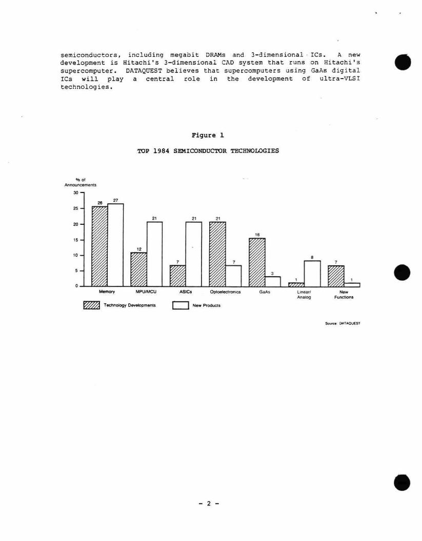
semiconductors, including megabit DRAMs and 3-dimensional - ICs. A new development is Hitachi's 3-dimensional CAD system that runs on Hitachi's supercomputer. DATAQUEST believes that supercomputers using GaAs digital ICs will play a central role in the development of ultra-VLSI technologies.
Figure 1
TOP 1984 SEMICONDUCTOR TECHNOLOGIES
% oI Announcemiants
3 0 - 1
J5 -
1 S -
10 -
Memory MPU/MCU
d Technology OeveIopments
ASICs Optoelectronics
I New Products
GaAs Linear/ Analog
New Functions
Source: DATAOUEST
- 2 -
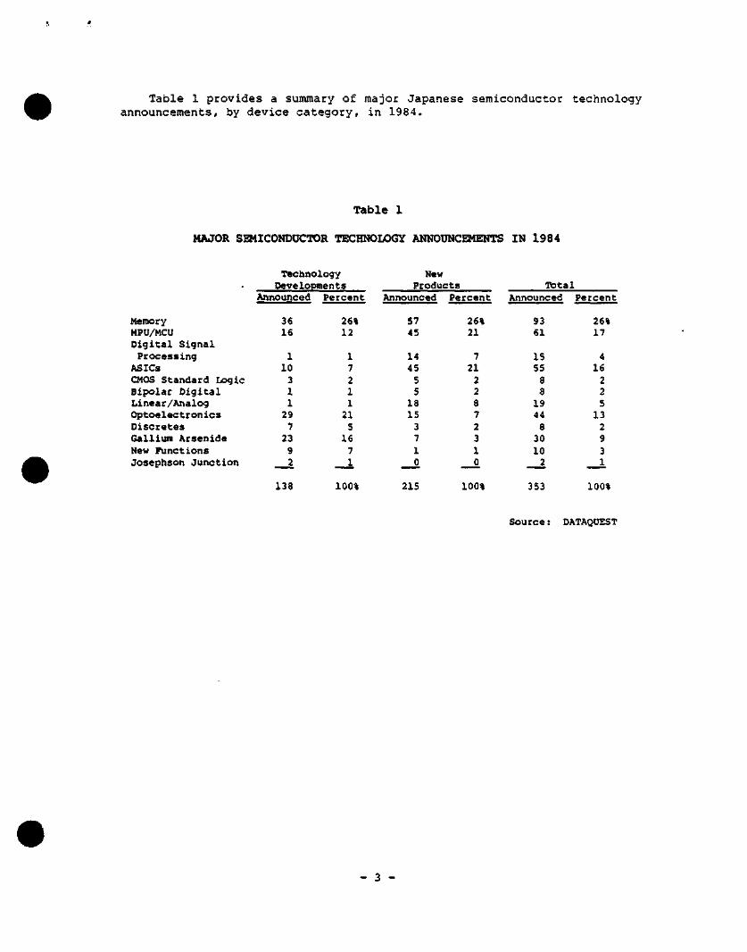
Table 1 provides a summary of major Japanese semiconductor technology announcements, by device category, in 1984.
Table 1
MAJOR SEMICONDUCTOR TECHNOLOGY ANNOUNCEMENTS IN 1984
Memory MPU/MCU Digital Signal Processing
ASICs CMOS Standard Logic Bipolar Digital Linear/Analog Optoelectronics Discretes Gallium Arsenide New Functions Josephson Junction
Technology Developments
Announced
36 16
1 10 3 1 1 29 7 23 9 2
Percent
26% 12
1 7 2 1 1 21 5
16 7 1
New Products
Announced
57 45
14 45 5 5 18 15 3 7 1 0
Percent
26% 21
7 21 2 2 8 7 2 3 1 0
Total Announced
93 61
15 55 8 8 19 44 8 30 10 2
Percent
26% 17
4 16 2 2 5
13 2 9 3
— I
138 100% 215 100% 353 100%
Source: DATAQUEST
- 3 -
1984 JAPANESE ELECTRONICS SHOW
The 1984 Japan Electronics Show was held in Tokyo in October with the theme of "Growing New Media and State-of-the-Art Technology." Sponsored by the Electronic Industry Association of Japan (EIAJ), the show offered 2,065 exhibit booths displayed by 675 companies from 18 countries. DATAQUEST observed the following trends at the show:
• Japanese semiconductor makers expect strong demand from Nippon Telegraph and Telephone's (NTT) Character and Pattern Telephone Access Information Network System (CAPTAIN)
• Prototypes of 1Mb DRAMs and 256K SRAMs
• Gallium arsenide memories with IK and 4K densities
o High-output semiconductor lasers (more than 25 milliwatts)
• Wide acceptance of gate array products
9 Promotion of industrial parks by Japanese prefectures as part of MITI's Technopolis program and by South Korea
Semiconductor highlights included Mitsubishi Electric's 1Mb DRAM prototype, and 256K SRAM prototypes by Mitsubishi and Toshiba. Hitachi displayed a photograph of its 1Mb DRAM. DATAQUEST believes that 1.3 micron geometries will be used for mass production of 1Mb DRAMs and 256K SRAMs within two to three years.
' In the area of microprocessors, Japanese makers displayed 4-bit and 8-bit CMOS MPUs, while NEC and Mitsubishi displayed their original MPU series. The major manufacturers are presently developing 32-bit MPUs.
The main logic products exhibited were high-speed CMOS standard logic and high-speed TTL, due to the expected surge in demand. Table 2 lists the major products introduced at the show.
- 4 -
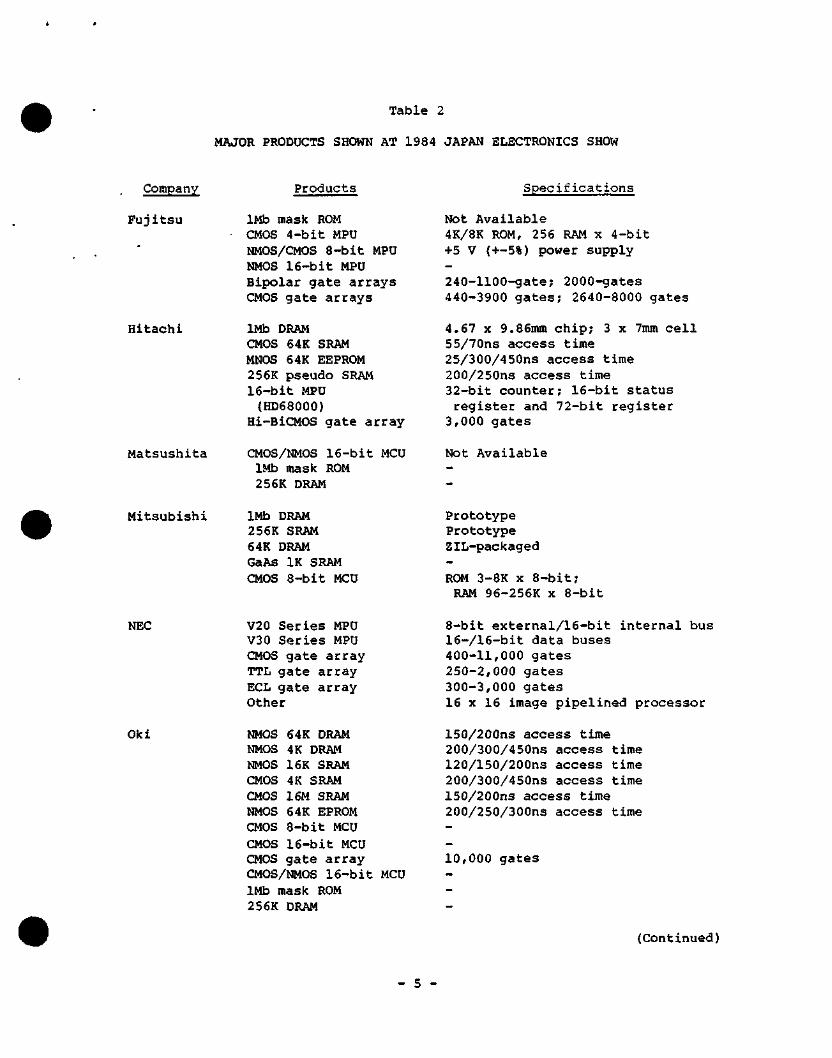
Table 2
MAJOR PRODUCTS SHOWN AT 1984 JAPAN ELECTRONICS SHOW
Company
Fujitsu
Hitachi
Matsushita
Products
1Mb mask ROM CMOS 4-bit MPU NMOS/CMOS 8-bit MPU NMOS 16-bit MPU Bipolar gate arrays CMOS gate arrays
1Mb DRAM CMOS 64K SRAM MNOS 64K EEPROM 256K pseudo SRAM 16-bit MPU (HD68000)
Hi-BiCMOS gate array
CMOS/NMOS 16-bit MCU 1Mb mask ROM 256K DRAM
Specifications
Not Available 4K/8K ROM, 256 RAM x 4-bit +5 V (+-5%) power supply
240-1100-gate; 2000-gates 440-3900 gates; 2640-8000 gates
4.67 X 9.86mm chip; 3 x 7mm cell 55/70ns access time 25/300/450ns access time 200/250ns access time 32-bit counter; 16-bit status register and 72-bit register 3,000 gates
Not Available
Mitsubishi 1Mb DRAM 256K SRAM 64K DRAM GaAs IK SRAM CMOS 8-bit MCU
Prototype Prototype ZIL-packaged
ROM 3-8K X 8-bit; RAM 96-256K x 8-bit
NEC
Oki
V20 Series MPU V30 Series MPU CMOS gate array TTL gate array ECL gate array Other
NMOS 64K DRAM NMOS 4K DRAM NMOS 16K SRAM CMOS 4K SRAM CMOS 16M SRAM NMOS 64K EPROM CMOS 8-bit MCU CMOS 16-bit MCU CMOS gate array CMOS/NMOS 16-bit MCU 1Mb mask ROM 256K DRAM
8-bit external/16-bit internal bus 16-/16-bit data buses 400-11,000 gates 250-2,000 gates 300-3,000 gates 16 X 16 image pipelined processor
150/200ns access time 200/300/450ns access time 120/150/200ns access time 200/300/450ns access time 150/200ns access time 200/250/300ns access time
10,000 gates
(Continued)
- 5 -
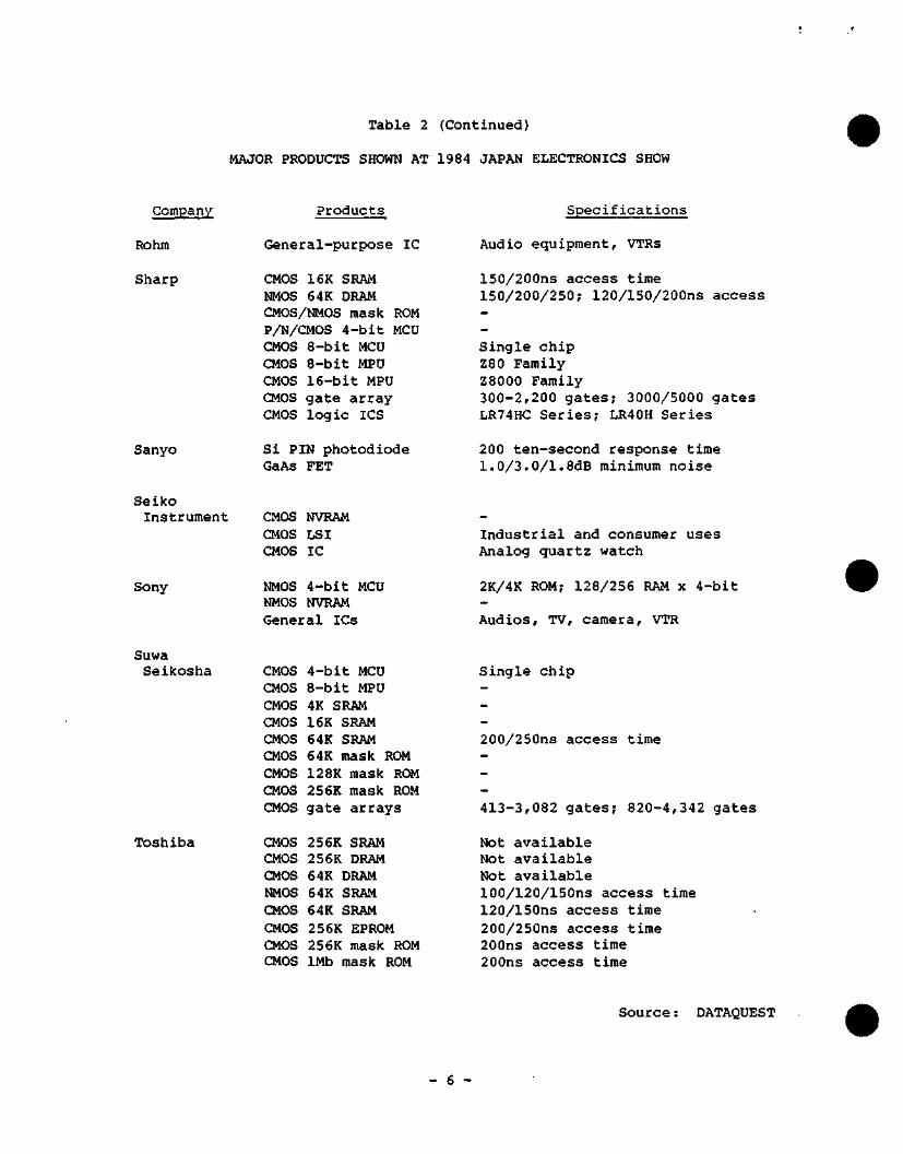
Table 2 (Continued)
MAJOR PRODUCTS SHOWN AT 1984 JAPAN ELECTRONICS SHOW
Company
Rohm
Sharp
Sanyo
Products
General-purpose IC
CMOS 16K SRAM NMOS 64K DRAM CMOS/NMOS mask ROM P/N/CMOS 4-bit MCU CMOS 8-bit MCU CMOS 8-bit MPU CMOS 16-bit MPU CMOS gate array CMOS logic ICS
Si PIN photodiode GaAs FET
Specifications
Audio equipment, VTRs
150/200ns access time 150/200/250; 120/150/200ns access
Single chip Z80 Family Z8000 Family 300-2,200 gates; 3000/5000 gates LR74HC Series; LR40H Series
200 ten-second response time 1.0/3.0/1.BdB minimum noise
Seiko Instrument
Sony
CMOS NVRAM CMOS LSI CMOS IC
NMOS 4-bit MCU NMOS NVRAM General ICs
Industrial and consumer uses Analog quartz watch
2K/4K ROM; 128/256 RAM x 4-bit
Audios, TV, camera, VTR
Suwa Seikosha
Toshiba
CMOS 4-bit MCU CMOS 8-bit MPU CMOS 4K SRAM CMOS 16K SRAM CMOS 64K SRAM CMOS 64K mask ROM CMOS 128K mask ROM CMOS 256K mask ROM CMOS gate arrays
CMOS 256K SRAM CMOS 256K DRAM CMOS 64K DRAM NMOS 64K SRAM CMOS 64K SRAM CMOS 256K EPROM CMOS 256K mask ROM CMOS 1Mb mask ROM
Single chip
200/250ns access time
413-3,082 gates; 820-4,342 gates
Not available Not available Not available 100/120/150ns access time 120/150ns access time 200/250ns access time 200ns access time 200ns access time
Source: DATAQUEST
- 6 -
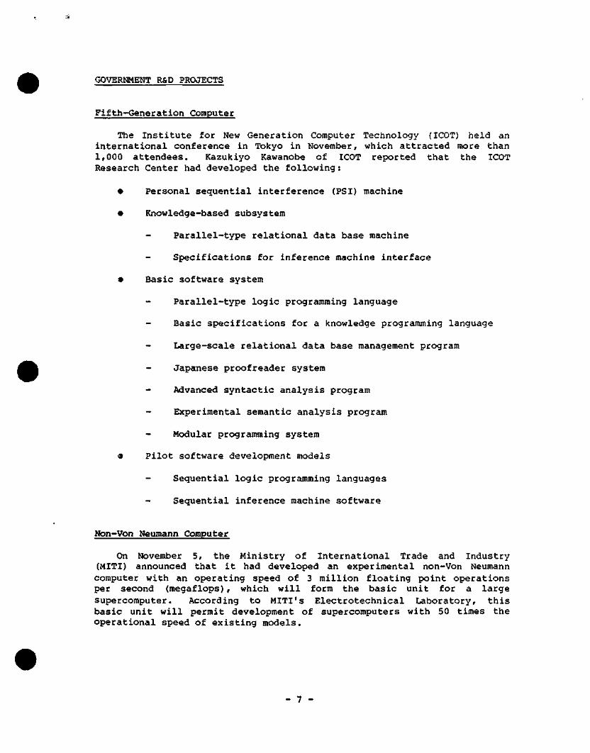
GOVERNMENT R&D PROJECTS
Fifth-Generation Computer
The Institute for New Generation Computer Technology (ICOT) held an international conference in Tokyo in November, which attracted more than 1,000 attendees. Kazukiyo Kawanobe of ICOT reported that the ICOT Research Center had developed the following;
• Personal sequential interference (PSI) machine
• Knowledge-based subsystem
Parallel-type relational data base machine
Specifications for inference machine interface
• Basic software system
Parallel-type logic programming language
- Basic specifications for a knowledge programming language
Large-scale relational data base management program
Japanese proofreader system
- Advanced syntactic analysis program
Experimental semantic analysis program
Modular programming system
9 Pilot software development models
Sequential logic programming languages
Sequential inference machine software
Nbn-Von Neumann Computer
On November 5, the Ministry of International Trade and Industry (MITI) announced that it had developed an experimental non-Von Neumann computer with an operating speed of 3 million floating point operations per second (megaflops) , which will form the basic unit for a large supercomputer. According to MITI's Electrotechnical Laboratory, this basic unit will permit development of supercomputers with 50 times the operational speed of existing models.
- 7 -
Optical Communication
On November 14, MITI announced that it plans to launch a feasibility study on international cooperation between Japan and Europe for integrated optical information transmission control technology. A study group of five to ten representatives from government offices, universities, NEC, Fujitsu, and Mitsubishi Electric were sent in November to visit the United Kingdom, France, West Germany, and the Netherlands to exchange opinions.
Supercomputers
Supercomputer technology is rapidly entering the commercial market. In October, Hitachi introduced a 3-dimensional CAD system for developing megabit DRAMs, high-function MPUs, and superlattice devices, which runs on its supercomputer (see DATAQUEST newsletter entitled "Hitachi Announces CAD System for 3-Dimensional Analysis," October 29, 1984). In a separate move, Amdahl announced that it would begin selling Fujitsu's VPIOO and VP200 supercomputers in the United States in 1985. Hitachi and NEC are expected to follow Fujitsu's lead. In Japan, there is growing interest in using GaAs digital ICs in next-generation supercomputers. Since FY1981, the Science and Technology Agency (STA) has run the Perfect Crystal Project under the leadership of Junichi Nishizawa of Tohoku University to develop defect-free GaAs single crystals for digital ICs. Currently, about 22 to 23 tons of gallium is used in Japan. A serious shortage of GaAs is expected because of the strong demand for GaAs in LEDs and semiconductor lasers for compact disks and optical communication.
NEW RESEARCH LABS
Konishiroku Photo plans to establish the Konica High Technology Laboratories in southern California by June 1986, The new research facility will be operated in cooperation with four local universities, including the University of Southern California (USC). According to President Megumi Ide, ¥1 billion ($4.2 million) will be invested in the facility annually (announced December 18).
Mitsubishi Electric is investing vl8 billion ($75 million) in a new research building at its LSI Research Center in Itami, Hyogo Prefecture, to develop next-generation VLSI, including 4Mb DRAMs (announced December 14).
Nippon Telegraph and Telephone (NTT) plans to invest V7 billion ($28.6 million) in a synchrotron at its Atsugi Laboratory to conduct R&D in super VLSIs, such as 64Mb DRAMs. Construction will begin in 1985, with operation scheduled for 1988 (announced November 6).
- 8 -
Tokyo Electron Ltd. (TEL) is investing " 2.0 billion ($8.3 million) in a research laboratory at its Nirasaki Works in Yamanashi Prefecture to conduct technical research on ultra-LSI manufacturing equipment. The current staff of 50 researchers will be expanded to 100 within three years (announced November 21).
Toshiba is building a design center in Kawasaki, Kanagawa Prefecture, for the Toshiba Microcomputer Engineering Corporation (TMEC). Scheduled for completion in April 1985, the center will have the latest CAD systems to design logic ICs and LSIs and to develop microcomputer software. TMEC expects to raise ¥3000 million ($1.25 million) in capital (announced October 24).
TECHNOLOGY DEVELOPMENTS
The megabit era is approaching. Fujitsu, Hitachi, Mitsubishi Electric, NEC, Oki Electric, and Toshiba have begun mass production of 256K DRAMs and have already manufactured experimental 1Mb DRAMs. Hitachi and NTT announced their 1Mb DRAMs at ISSCC 1984, while NEC, Mitsubishi, and Toshiba will announce 1Mb DRAMs at ISSCC 1985. Research in 256K SRAMs is proceeding rapidly, with Hitachi, NEC, and Toshiba planning to present papers at ISSCC 1985.
Memory
The following memory developments were announced during the fourth quarter of 1984:
Hitachi—A 45ns, 256K CMOS SRAM with variable impedance loads; 32K X S-bit organization; 200mW at 10-MHz active power dissipation; polycide Vss-line used in a 95-micron-square memory cell (to be presented at ISSCC 1985)
A 95ns, 256K CMOS EPROM with 12mW power dissipation at 1-MHz cycle time; 0.5ms/byte average programming time with voltage range of 11-14 volts; 12mW active operating power (to be presented at ISSCC 1985)
Matsushita—An 8K content-addressable and re-entrant memory using 20 micro CMOS; 100ns cycle time; 30 x 36 micron memory cell (to be presented at ISSCC 1985)
Mitsubishi—A 1Mb DRAM with 2.5 million transistors and 1.0 micron design rule and 256K SRAM; both displayed at Electronic Show '84 (announced October 1984)
A 90ns, 1Mb DRAM with multibit test mode using half Vcc biased memory cell and a reduced electric field; shared sense amplifier design and continuous nibble mode; 65mm-square die (to be presented at ISSCC 1985)
- 9 -
A 45ns, 256K CMOS SRAM; peak current of 45mA by usirig an address transition activated circuit with a tri-level wordline circuit (to be presented at ISSCC 1985)
NEC—A 55ns, 256K CMOS SRAI-l using optimized poly load resistors, buried isolation and Ti polycide to achieve lOmW standby power in a 40.7mm square die (to be presented at ISSCC 1985)
A 64K X 4 DRAM and a 256 x 4 serial readout memory with 35ns access time; for graphic data pickup from any location (to be presented at ISSCC 1985)
An NMOS 85ns, 1Mb DRAM; trench capacitors and extra polycide interconnect layer to develop 43.2mm-square circuit in a 300-mil plastic DIP (to be announced at ISSCC 1985)
A 4K (16-level) cell storage, single transistor DRAM with 4 x density storage (to be announced at ISSCC 1985)
Seiko Instrument & Electronics—An experimental nonvolatile random access memory (NVRAM) that combines RAM and EEPROM; developed using a perpendicular accelerated channel injection MOS (PACMOS) method; writing voltage for memory storage less than 5 volts; 7 transistors per bit; sampling from 1985 with plans to mass produce 16K NVRAMs by 1986 (announced December 3)
Toshiba—An NMOS 1Mb DRAM with 7Gns access,, using 1.2-micron design rule and Toshiba's Buried Oxide Isolation technology; two-level metal; 300-mil, 18-pin standard OIL; 4.78 x 13.23mm chip with 2,250,000 transistors and capacitators; 5.0 x 6.4 micron memory cell size; NMOS process and double-layer metal; 270mW operating power consumption and 15mW at standby (announced November 1)
A new memory cell (folded capacitor cell) that features a groove etched in the isolation field of two neighboring devices and oxide film buried in the groove; permits an increase in the capacitor area while reducing the memory cell size; marks a major step toward development of ultra-LSI devices greater than 4Mb (announced November 19)
A 17ns, 64K CMOS SRAM using a four-transistor cross-coupled flip-flop memory cell with high resistivity load composed of the second polysilicon; 12.5 x 21.5 micron cell; 3.86 x 6.99mm die in 300-mil-wide 22-pin plastic DIP (to be presented at ISSCC 1985)
A 256K flash EEPROM with a single transistor cell; 5.7 x 5.8mm square chip size achieved using 2.0-micron design rule and triple polysilicon technology (to be presented at ISSCC 1985)
- 10 -
Microprocessors/Microcontrollers
Hitachi—An experimental 32-bit CMOS MPU capable of processing 5 MIPS; 50ns execution cycle time in standard operations; 1.3-.Tiicron design rule; two-layer aluminum interconnect method; 300,000 units integrated on a 6.5 x 9.0mm chip; 20-MHz speed; 400 to 500-mmW power consumption in test model and 1 watt in commercial model; sampling from 1987 (announced November 15)
An 8-bit CMOS MPU with instruction controlled register file and ROM, using 2-micron rule (to be presented at ISSCC 1985)
NEC—joint ventures with Yokogawa Hewlett-Packard, Sophia Systems, Tektronix, and Digital Research for joint development of V Series MPU support systems (announced in May and November)
An agreement with Corvus Systems to jointly develop a CMOS single-chip controller with a 1.6-micron rule and 100,000 transistors for use in Corvus' Omninet local area network (LAN) that will offer 4Mb/sec transmission speed (announced November 15)
NTT Atsugi—A single chip, 5.6-MFLOP, 80-bit floating-point processor using 1.2-micron N-well CMOS technology; 50K gates and 15K memory; developed by hierarchical design automation system (to be presented at ISSCC 1985)
Digital Signal Processing
Tohoku University—A 2-MHz pipelined image-processing chip designed with a 5-micron NMOS process; multiple ion implant quaternary logic resulting in a four-fold reduction in complexity (to be presented at ISSCC 1985)
Application-Specific ICs (ASICs)
Fujitsu—A 240K transistor CMOS masterslice array with flexible memory and channel allocation (to be presented at ISSCC 1985)
A Ins CMOS gate array series with configurable 15ns 12K memory and 20K logic gates; 1.5-micron twin well process (to be presented at ISSCC 1985)
Hitachi—A bipolar/CMOS 1,300-gate array with the high-speed features of an ECL and low power consumption of CMOS; O.lSmW power dissipation; 0.8ns delay; complete merging of CMOS and bipolar at basic cell level; Hi-BiCMOS 1,000 to 3,0G0-gate products to be introduced within one year (announced October 9)
A 4K CMOS gate array with automatically generated test circuits; 2-micron process on a 7.2 x 7.0mm square chip; 98 to lOO percent dc fault testing with logic design restrictions in a chip area of 5 percent (to be presented at ISSCC 1985)
- 11 -
Mitsubishi—A 1.5-micron CMOS gate array with configurable ROM and RAM; 3,000-gate array with double word line memory addressing on a 9.9 X 9.8iraTi chip (to be presented at ISSCC 1985)
Nippon Telegraph and Telephone—A high-density bipolar gate array with 0.32ns processing speed and 5,000 gates; processing time three to four times conventional arrays; Icm-square silicon substrate; to be used as logic for supercomputers and telecommunications equipment (announced October 19)
An BOps 2,500-gate bipolar microcell array using 1-micron rule; 7.5ns, 16-bit multiplier achieved (to be presented at ISSCC 1985)
Toshiba—A triple-level, wired, 24K-gate CMOS array using 2-micron design rule on a 12.8mm-square chip (to be presented at ISSCC 1985)
CMOS Standard Logic
Hitachi—A low-temperature CMOS 8 x 8-bit multiplier with sub lOns speeds; 5mW and 460mW power dissipation (to be presented at ISSCC 1985)
A 6GHz ECL frequency divider using sidewall base contact structure; 45mW and 9mW dissipation (to be presented at ISSCC 1985)
Bipolar Digital
No major announcements.
Linear/Analog
Hitachi—A CMOS video filter using switched capacitator 14-MHz circuits; 2-micron design rule (to be presented at ISSCC 1985)
Optoelectronics
Asahi Chemical—A new organic semiconductor that is highly sensitive to a wide wavelength area ranging from infrared to visible light; used to produce a photoconductor drum for commercial LED printers, liquid crystal printers, laser printers, and intelligent copy machines (announced November 26)
Kokusai Denshin Denwa (KDD)—A hetero-structured avalanche photo diode (HAPD) for next-generation long-distance underwater optical cable systems; 50 percent reduction in transmission loss using 1.55-micron wavelength; high sensitivity and response (announced in October)
Matsushita Electric—World's first optical integrated device with semiconductor laser and transistor functions; for next-generation optical memories and inverters; enables large increase in optically transmitted information (announced October 30)
- 12 -
NEC—A long-wavelength semiconductor laser with 140 mmW of continuous operating power; consists of indium, GaAs, and phosphorous, and emits 1.3-iiiicron wavelength laser; to be used for remote sensing and longdistance optical communication (announced November 29)
Rohm—A compact disc semiconductor laser (RLD-78A) produced using molecular beam epitaxy (MBE); technical breakthrough made possible by producing most suitable characteristics during a single photomask process; vacuum used for laser fabrication process; equal growth layers and 88,000 laser chips possible from a 75mm wafer; one hour for wafer growth (announced November 29)
Sharp—An interference-type laser with an 780-nanometer oscillation wavelength, using Sharp's original twin resonator structure (IRI-VSIS); stable oscillation axis mode (announced December 14)
Toshiba—Quantity production technology for optical communication LEDs using metal organic chemical vapor deposition (MOCVD); productivity increased 15 times over conventional liquid phase epitaxial (LPE) methods; sample shipments of MOCVD-produced LEDs from mid-1985; ¥5,000 ($20.40) quantity price (announced November 14)
Image Sensors
Fuji Photo Film—Solid state image pick-up devices for 8mm VTR and electron still camera; test manufactured CCD with 400,000 picture elements; experimental CCD with 800,000 picture elements (announced October 29)
Japan Research Development Corporation—A semiconductor image pickup device (electrostatic induction-type photo sensor) capable of photographing in starlight; sensitivity claimed to be 1,000 times higher than conventional image pickup devices (announced November 21)
Matsushita Electronics—Small, low-noise, charge-coupled devices (CCD) using two types of technologies (heat process and IG process) to produce epitaxial wafer; 40 percent space reduction possible using new technologies (announced December 11)
A 490 7t 404 element CCD imager for a single-chip color camera; 5.86 X 7.13mm; S/N ratio of 55dB under scene illumination of 200 Ix (to be presented at ISSCC 1985)
A multichip, constant-type CCD linear image sensor that can read A4-si2e document with 16 lines/mm resolution and S/N ratio of 48dB (to be presented at ISSCC 1985)
Mitsubishi—A 480 x 400-element image sensor with charge sweep device; 10 x 16-micron-square pixel size (to be presented at ISSCC 1985)
- 13 -
Sharp—A 580 x 500 element interline-transfer CCD imager with a shallow flat P well that incorporates CCD shift registers and photodiodes; N-type substrate for blooming suppression; 32 percent aperture ratio (to be presented at ISSCC 1985)
Discrete
NEC—A silicon bipolar 6.2-GHz, BOOmW frequency divider for local oscillators in a microwave communication system; self-aligned bipolar transistors with 1.25-micron lithography (to be presented at ISSCC 1985)
Sony—An ultra-thin-film transistor (MOS FET) only 0.02 microns thick; operating speed two to three times faster than conventional thin-film transistors; practical use in flat plane liquid crystal TVs, facsimiles, and two-story SRAMs in the future (announced October 15)
Toshiba—Bipolar-type MOS FET featuring high response of MOS FETs and large current capability of bipolar transistors; 500- and 1,000-volt prototypes; 1.0 to 1.2-microsecond switching speed; on resistance of 0.1-0.2 ohm; 3-micron rule; used as power modules for motor control systems (announced in October)
Gallium Arsenide
Hitachi/Optoelectronics Joint Research Laboratory—A GaAs single-crystal wafer with inequality in transistor threshold voltage that is one-third that of conventional devices; initial step toward development of GaAs LSIs (announced November 9)
Matsushita Electronic—A GaAs self-aligned FET that will enable production of MMICs (microwave monolithic ICs); noise frequency at 12 GHz is l.SdB; 6-volt breakdown voltage (announced December 7)
NEC—An ultra-high-speed GaAs logic IC; a 12-bit x 12-bit extended-type parallel multiplier consisting of 1,083 logic gates, 3,546 transistors, 1,136 diodes, and 45 resistors; 4ns maximum operating speed; 170ps delay time per gate; 2.5W power consumption (1.7 mmW per gate); commercialization within two years (announced December 10)
A GaAs 4K SRAM for high-speed computer cache memory, 2.4ns address access time with I.IW power dissipation; IK by 4 bit (to be presented at ISSCC 1985)
Nippon Telegraph and Telephone—A GaAs monolithic IC for microwave band switching and milliwave band amplication for multibeam, large-capacity communications satellites; eight switches integrated on a 4.5 x 4.0mm chip; power consumption of 10 watts; designed for l-GHz band and capable of up to 30 GHz (announced in October)
Oki—A 390ps 1,000-gate GaAs gate array using super-buffered FET logic (to be presented at ISSCC 1985)
- 14 -
optoelectronics Joint Research Laboratory—A dislocation-free, GaAs 2-inch single crystal with no surface defects; suitable for lasers and LEDs, but not for ICs (announced December 14)
Toshiba—A high-performance transistor (selectively-doped transistor) using structure similar to Fujitsu's high-electron mobility transistor (HEMT); 1.0-micron layers of GaAs and GaAlAs on a GaAs substrate; 30 percent noise reduction and 50 percent increased amplification over conventional GaAs FETs in 12- to 30-gigahertz microwave range (announced November 13)
Josephson Junction
Hitachi—^World's first ultra-conductive transistor using Josephson junction device for control terminal; source and drain placed 0.2 micron apart to form channel; potential for 20ps switching speed and 5mW power consumption; 200mm-thick Pb superconducting terminal; 300nm-thick P-type silicon crystal; 40nm-thick silicon oxidized film; plans for a ring oscillator within one year to confirm device performance (announced November 10)
NEC—A 350ps Josephson 4 x 4-bit parallel multiplier and ImW dissipation; built with 249 resistor-coupled Josephson logic gates; Pb-alloy process with 5-micro minimum line widths and junction diameters (to be presented at ISSCC 1985)
New Semiconductor Functions
NEC—A diamond thin-film over silicon for 3-dimensional ICs; direct current flow electrical discharge method used to form the diamond layer in a vacuum chamber by saturating the silicon layer with methane and hydrogen gases; one-micron thick film over 2cm-square area produced (announced in October)
Tokyo Industrial University—A one-chip biosensor capable of detecting sugar and urea in blood and urine samples; 2.5 x 0.4mm sapphire-coated silicon substrate on which two transistors bearing enzymes are designed; potential use as a home health diagnostic system (announced in October)
Toshiba—Improved 3-dimensional IC production technology; development of an experimental O.Smm-square single-crystal silicon substrate; 1.3-micron-thick isolation layer of tungsten coated on bottom IC layer before growing second IC layer; even temperature distribution allowed by tungsten coating; test manufacturing of a 2-layered, 3-D IC scheduled for January (announced November 21)
- 15 -
CAD Systems
Hitachi—World's first CAD system for 3-dimensional analysis for developing 1Mb to 64Mb DRAMs, PMUs, superlattice devices, 3-D ICs, and bipolar devices; runs on Hitachi supercomputer at one-hundredth current processing times; displays electrical and physical characteristics of CMOS and bipolar devices (announced on October 19)
Manufacturing Processes
Dai Nippon—A new photomask capable of producing ultra-high-frequency FETs with 0.3-micron line widths; resolution achieved by using electron beam lithography and highly-automated clean room line; 8Mb memories possible with 0.3-micron design rule (announced in October)
Hitachi—A highly sensitive photoresist that permits 0.8-micron geometries using an organic silicon solution that reacts to ultraviolet rays with extremely short wavelengths; 4Mb devices possible by eliminating the pre-etching process (announced in October)
Electron beam equipment capable of positioning circuits within 0.05 micron and automatically measuring the pattern at high speed and an accuracy of 0.01 micron; automatically measures 100 to 200 positions per hour on a single wafer; to be used for 16Mb DRAM development; titanium-doped tungsten used as electrical field emission electron source and a new optical system 1,000 times brighter than conventional beams (announced in October)
NEC—A multi-layer processing technology called ELVIC (elements level vertically integrated circuit) that doubles LSI densities and allows fabrication of composite LSIs using different materials and functions; PMOS and NMOS transistors used to form 31-stage CMOS ring oscillator; 30 patent applications submitted and plans to commercialize LSIs using technology within two years (announced December 4)
Research on VLSI manufacturing and analysis of material structures by using the synchrotron orbital radiation generator at the National Laboratory for High Energy Physics in the Tsukuba Science City; NEC equipment to be established in the laboratory to develop VLSIs larger than 1Mb (announced December 12)
Manufacturing Equipment
On November 28, 15 major semiconductor equipment makers, including Canon, Nippon Kogaku, Takeda Riken, and Anelva, agreed to establish a Semiconductor Manufacturing Equipment Council in January. The council will conduct joint research and information exchange on product technology and distribution, product standardization, negotiations with government agencies, and compilation of statistics. The group will work with MITI's Industrial Machinery Division.
- 16 -
Hitachi—World's first dust counter capable of detecting 0.05-micron dust particles; reflective power ten time stronger than conventional models by using helium cadmium laser instead of helium neon laser; permits development of 16Mb DRAM (announced November 8)
IC measuring technology that uses electron beams; wiring pattern of 100 to 200 points per hour on a wafer automatically measured to 0.01-micron accuracy; permits development of megabit VLSIs (announced November 8)
Kuwano Electric—High-speed burn-in equipment (BS-IOOO) for 64K and 256K DRAMs; capable of handling 9,600 units; being used at Oki Electric; sales to start in 1985 (announced November 19)
Nissin Electric—An ion implantation machine (NH-2DSD) capable of processing 450 wafers per hour; shipments beginning spring 1985 at ¥200 million ($833,000) per unit (announced December 4)
NTT/Eaton—An agreement to jointly develop high-current oxygen ion implantation equipment for next-generation VLSI production; NTT to provide SIMOX technology that involves injecting films; Eaton system to have 100 milliamperes of ion beam current and 200 electron KV acceleration voltage; first model to be shipped to NTT in late 1985 and world sales in 1986 (announced December 1)
Osaka University/JEOL Limited—An electron-beam nanometer lithography system capable of 10-nanometer line widths; to be used for next-generation gigabit memories in late 1990s; employs a field emission-type electron gun and a conical-shaped tungsten tip (0.5-micro radius) in the emitter (announced in October)
Test Equipment
Sony—^Wafer defect inspection equipment being developed at Kokubu Semiconductor plant in Kagoshima prefecture; designed for wafers used in high-resolution CCDs and 64K SRAMs (announced October 29)
Chemicals and Materials
Noritake—A ceramic substrate for thin-film ICs; glazed and non-glazed alumina; 0.7-micron thin film possible, but 0.25-micron process being developed (announced November 16)
NTT Ibaraki Lab—A new resist material for VLSI memories greater than 1Mb; 0.2-micron 2-level structure over 1-micron polymer resist; 0.7-micron circuit patterns possible (announced November 8)
- 17 -
Packaging
Fujitsu—A plastic chip carrier featuring inward curving of leads projected in four directions, 50 mils between leads, and small size suitable for mounting to ICs with large pin counts; this new package to be used for gate arrays (announced December 5)
Nippon Telegraph and Telephone—Plastic IC packaging to be introduced in telecommunications LSIs used in the Information Network System (INS) to lower costs (announced December 11)
Toshiba—A carbon dioxide gas laser engraver to mark IC packages (announced October 13)
MAJOR PRODUCT ANNOUNCEMENTS
Memory
Ricoh—Five mask ROM models; two models with 250/300ns access time (NMOS 512K and 1Mb) and three models with 200/250ns access time (CMOS 64K, 12K, and 256K) ; CMOS types compatible with Intel and TI's EPROMs (announced December 17)
Toshiba—64K SRAM (64K x 1) with 55ns access time; 1.5-micron design rule; 3.86 x 6.99mm chip; smallest chip size made by Japanese industry; SOOmW power dissipation during operation and 5.5mW at standby; 22-pin 300-mil plastic DIP; sample price ¥12,000 ($49) ; monthly production of 50,000 units from January (announced November 27)
Microprocessors
Hitachi—Two plastic-package 16-bit MPU models for HD68000 series; a 900-rail unit, pin-compatible with 64-pin OIL ceramic type (model P) and a 64-pin OIL in a shrunken package; sampling price of ¥6,500 ($27) and mass production price of ¥4,500 ($19); monthly production to be increased to 75,000 units in 1985 (announced December 5)
Sony—A series of 4-bit MCUs (SPC500 Series) featuring CPU core architecture that allows the user to add peripheral functions without making alterations (announced in October)
Four models of CMOS 4-bit single-chip MPUs (SPC5000 Series) with 4K ROMs; two types available; high-speed type (1.9 microsecorids) priced at ¥1,800 and ¥2,000 ($7.35 and $8.16) and general type (3.8 microseconds) at ¥2,000 and ¥2,000 ($8.16 and $8.98); piggy-back type ¥20,000 ($81.60) (announced on October 4)
Tokyo Sanyo—A 4-bit CMOS MCU with a 950ns cycle time; for use as a control signal processor for printers, floppy drives, VTRs, and tape decks; priced at ¥450 ($1.80) (announced in October)
- 18 -
Toshiba—Two CMOS single-chip LSIs for interface control; Model TC8577P for serial interface; Model TC8578P for parallel type; sample price ¥l,OOQ ($4.10); monthly production of 50,000 units starting in February 1985 (announced October 19).
Two NMOS 16-bit MPUs of ZSOOO line; 6 MHz and 48-pin DIP for TMPZ8003-6 and 6 MHz and 40-pin DIP for TMPZ8004C-6; sample prices ¥5,500 ($22.45) and ¥5,000 ($20.40) respectively; monthly production of 10,000 units starting in 1985 (announced November 10)
Digital Signal Processing
NEC—A single-Chip LSI for adaptive differential pulse-code modulation (PCM) operation necessary for voice mail system and voice answering equipment; compression and expansion of voice digital signal; sample price ¥10,000 ($40.80) (announced October 5)
Application-Specific ICs (ASICs)
Mitsubishi—Nine models of CMOS gate arrays, ranging from 238 to 8,096 gates; initial production at 200,OOO units per month (announced October 26)
Ricoh—CMOS gate array, series of 500, 1,000, 1,500, 2,500, and 3,800 gates to existing 400 to 1,500 gate array series (announced December 14)
Sharp—A personal workstation (LZ9D100) for gate array development; equipped with conversation type high-speed logic simulator so that logic circuit operations can be checked while talking to workstation; priced at ¥5.5 million ($22,450) beginning in March 1985 (announced October 2)
Toshiba—Two CMOS gate array models with 1.5ns gate delay; 6,000-gate model (TC17GM61) with IK SRAM built in and 540-gate model (TC17G005); available in April (announced November 21)
A large, full-custom LSI (super integration) with Z80 as core and various peripheral circuits; shipments starting in 1985 (announced December 17)
CMOS Standard Logic
Sanyo Electric—A CMOS logic device (VLC8930) to scramble voice signals transmitted by cordless phones and wireless equipment; voice signals compressed and expanded using a variable delay circuit; 3.6mW power consumption; priced at ¥1,500 ($6.12); to be exported in cordless phone next spring (announced in October)
Tokyo Sanyo—A high-speed CMOS standard logic line (I,C74HC series) featuring an S.Ons delay time; includes logic gates, inverters, and flip-flop devices (announced in October)
- 19 -
Bipolar Digital
No major announcements.
Linear/Analog
Pioneer Electronic—A surface wave device that converts 668- to 674-MHz cable TV signals to 50-MHz TV signals; to be used in Pioneer's CATV equipment and sold as components; monthly production 100,000 units (announced October 13)
Sanyo Electric—World's first ICs for secret communication and two noise-proof LSIs for remote control; secret communication IC priced at ¥1,500 ($6.10), remote control and central control equipment IC at ¥3,000 ($12.25), and remote control and peripherals at ¥2,000 ($8.16) announced October 4)
Toshiba—Two telephone ICs (TA31024N/TA31025N) on a single chip that contains all the functions for putting voice signals on telephone circuits; 15V line voltage; 150-mmA line current; 500-mmW power consumption; sampling at ¥1,500 ($6.12); monthly production of 100,000 units starting in spring 1985 (announced October 2)
Optoelectronics
Sony—Two visible optical semiconductor lasers produced using metal organic chemical vapor deposition (MOCVD); SLDIOIUI for video disk priced at ¥7,000 ($28.60); SLDIOIU for compact disks at ¥5,000 ($20.40); 780-nanometer wavelength; 5-mmW output; 100,000-hour life at room temperature; monthly production of 150,000 units starting in 1985 (announced November 14)
Suwa Seikosha—Two MOS solid-state image pickup devices; 59,536 and 186,725 picture elements; to be applied to VTR cameras and robot visual systems; Suwa Seikosha to enter video processing equipment market (announced November 2)
Toshiba—A high-power semiconductor laser for optical disk filing equipment (TOLD500); capable of narrowing laser beam diameter to 1 micron at 30 mmW; peak wavelength of 810 nanometers (announced December 19)
Discretes
Hitachi—Four super-low-noise bipolar transistors; three models with 6-GHz cut-off frequency, lldB voltage gain, and 1.5dB noise, and one model with 7.5-GHz frequency, 12.5dB voltage gain and 1.2dB noise index; quantity production at ¥45 ($0.18) per unit for 10,000 unit orders (announced November 30)
- 20 -
Toshiba—Two bipolar MOSFETs; sample shipment of electric power module for motor controls planned in 1985; 500V model in March and lOOOV model in autumn (announced October 30)
Gallium Arsenide
Mitsubishi Electric—Five low-noise GaAs FET models for telecommunication receivers; MGF1405 (O.SdB at 4 GHz, 1.4dB at 12 GHz); MGF1302 (below 1.4dB at 4 GHz); MGF1303 (below IdB at 4 GHz, 2dB at 12 GHz) MGF1304 (below 0.7db at 4 GHz, 1.7dB at 12 GHz), MGF1305 (below 0.6dB at 4 GHZ, 1.6dB at 12 GHz); one FET model for consumer use (announced December 18)
Nippon Telegraph and Telephone—Two GaAs MMICs for future telecommunications satellite transponders; a monolithic single-chip switch IC with either switches integrated on a 4.5 x 4.0mm chip (one hundredth the size of conventional hybrid types) and a monolithic amplifier IC on a 2.0 x 2.0mm chip (announced October 18)
New Semiconductor Functions
No major announcements.
Josephson Junction
No major announcements.
CAD Software
Prime Computer Japan—A 3-dimensional CAD system (Prime Medusa); presently used at Japan Radio Corp. and Sony Tektronix (announced December 5)
Manufacturing Processes
No major announcements.
Manufacturing Equipment
Anelva—Deposition equipment using an ECR ion source; can be used for thin-film formation ranging from submicron-class VLSIs to chemical compound semiconductors; priced at ¥41 million ($167,350); processing capacity of 8 to 10 4-inch wafers per hour (announced October 17)
Komatsu—A commercial excimer laser with 12-watt average output and emission rate of 60 pulses per second; plans for 30-watt device in 1986; used as light source for ultra-VLSI lithography; mixture of krypton and
- 21 -
fluorine gases used; 1.2kW power supply and 280-millijoule maximum pulse energy; priced at ¥10 million ($40,300) (announced in November)
Nippon Seiko—A multiple-use exposure machine (TZ-800) capable of processing pattern exposure, including mask production, stepping, and wafer direct exposure; developed at Semiconductor Research Institute of Tohoku University in Sendai; sales from summer 1985 (announced November 7)
Toshiba/TOkuda Works—Plasma CVD equipment with nearly 100 percent automatic microcomputer control; 70 types of sensors for handling variety and increased production of thin-film semiconductors used for liquid crystal and solar cells; price ¥120 million ($490,000) production beginning in April 1985 (announced October 24).
A single-wafer reactive ion etching (RIE) machine to handle 6-inch wafers for 4Mb memories; 80 HIRRIE-lOO units to be produced and marketed by Tokuda from December; price ¥68 million ($277,550) (announced November 29)
Test Equipment
Matsushita Communication—A linear IC tester capable of processing 1200 ICs per hour; built around Z80 and employing ACTION high-level language for controlling measurement tasks; priced at ¥5 to ¥15 (R20,000-$61,000) (announced November 28)
Mitsui/Anritsu Electric—A laser prober system designed to locate defects in LSI logic chips; technology originally developed by Data Probe of Santa Clara which granted exclusive rights to Mitsui; shorter development time and no chip scratches possible; priced at ¥32 million ($131,000) (announced in October)
Takeda Riken—A logic LSI testing system {T3126) with throughput double that of existing model; test rate of 10 MHz; simultaneous testing of 4 IC units possible using two units of 48-pin test heads; price ¥45-65 million ($183,670 to 265,300) (announced November 27)
A 4Mb memory testing system (T3332) capable of handling 16 units at a time; 30-MHz test speed; potential for lowering test costs by 50 to 60 percent; priced at ¥70 million ($285,700); an auto-handler that handles eight units at a time {T3778) (announced in November)
Chemicals and Materials
No major announcements.
Packaging
No major announcements.
Sheridan Tatsuno Nagayoshi Nakano
- 22 -
JSIA Code: Newsletters
PRELIMINARY 1984 MARKET SHAKE ESTIMATES
SUMMARY
DATAQUEST's preliminary market share estimates show that the semiconductor revenues of the top nine Japanese semiconductor manufacturers grew 59 percent in dollars in 1984. Several major ranking changes also occurred. Most notably, NEC now ranks as the second largest merchant semiconductor manufacturer in the world, with 1984 revenues of $2,270 million, usurping Motorola's long hold on the number two spot.
JAPAMESE COMPANY REVENUES
Table 1 lists 1983 and 1984 total semiconductor revenues for the top nine Japanese semiconductor manufacturers. No changes in ranking occurred. While overall growth for these companies was 59 percent, several grew at significantly higher rates, including Fujitsu at 73 percent and Mitsubishi at 67 percent. The three revenue leaders, NEC, Hitachi, and Toshiba, grew 61 percent, 55 percent, and 59 percent, respectively. Sanyo and Sharp, ranked seventh and eighth, grew the slowest at 47 percent.
Table 2 analyzes the relative changes in market share experienced by the top nine Japanese manufacturers in 1984. This analysis measures the change in each company's percentage of total top nine revenues for each product line. NEC lost 4.5 percent of its market share in bipolar digital ICs, while Fujitsu gained 3.9 percent. In MOS, NEC, Fujitsu, and Mitsubishi gained the market share that the other six ccxnpanies lost. Toshiba picked up 2.4 percentage points in linear ICs and lost 4.8 percentage points in optoelectronics. Sharp was the big winner in optoelectronics, maintaining its position as world leader and gaining 3 percent in market share from its Japanese competitors.
© 1985 Dataquest Incorporated Jan. 2 ed.-Reproduction Prohibited
The content of this report represents our interpretaion and analysis ol information generally available to the public or released by responsible individuals in the subject companies, but is not guaranteed as lo accuracy or completeness It does not contain material provided to us in confidence by our clients Individual companies reported on and analyzed by DATAQUEST, may be clients of this and/or other DATAOUEST services This information is not furnished in connection with a sale or offer to sell securities or in connection with the solicitation of an offer to buy securities This firm and its parent and/or their officers, stockhoIders, or members of their families may, from time to time, have a long or short position in the securities mentioned and may sell or buy such securities
Azabu Heights, Suite 711, 1-5-10 Roppongi, Minato-ku, Tokyo 106, Japan 1290 Bidder Park Drive / San Jose, CA 95131 / (408) 971-9000 / Telex 171973
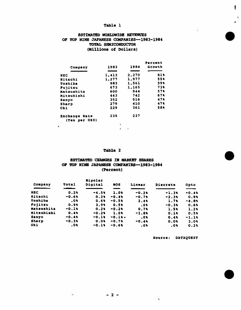
Table 1
ESTIMATED WORLDWIDE REVENUES OF TOP NINE JAPANESE C(»!PANIES—1983-1984
TOTAL SEMICONDUCTOR (Millions of Dollars)
Company
NEC Hitachi Toshiba Fujitsu Matsushita Mitsubishi Sanyo Sharp Oki
1983
1.413 1,277
983 673 600 443 352 279 229
1984
2,270 1,977 1,561 1,165
944 742 516 410 361
Percent Growth
61% 55% 59% 73% 57% 67% 47% 47% 58%
Exchange Rate 235 237 (Yen per 08$)
Table 2
ESTIMATED CHANGES IN MARKET SHARES OF TOP NINE JAPANESE CCMFANIES—1983-1984
(Percent)
Company
NEC Hitachi Toshiba Fujitsu Matsushita Mitsubishi Sanyo Sharp Oki
Total
0.2% -0.6%
.0% 0.9%
-0.1% 0.4%
-0.4% -0.3%
.0%
Bipolar Digital
-4.5% 0.2% 0.6% 3.9% 0.2%
-0.2% -0.1% 0.0%
-0.1%
HO5
1.0% -0.4% -0.5% 0.5%
-0.2% 1.0%
-0.1%. -0.7% -0.6%
Linear
-0.2% -0.7% 2.4% .0%
0.7% -1.8%
.0% -0.4%
.0%
Discrete
-1.3% -2.3% 1.7%
-0.3% 1.5% 0.1% 0.4% 0.0% .0%
Opto
-0.4% 0.9%
-4.8% 0.6% 1.2% 0.5%
-1.1% 3.0% 0.2%
Source: DATAQOEST
- 2 -
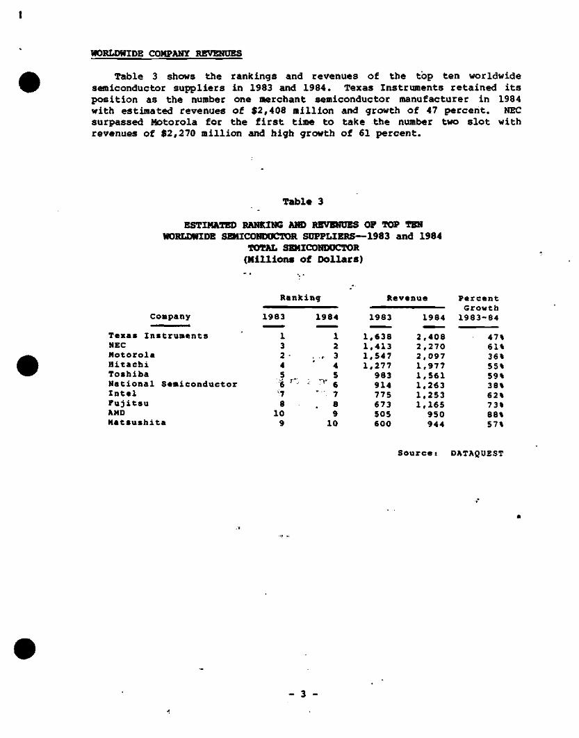
WORLDWIDE COMPANY RBVEITOES
Table 3 shows the rankings and revenues of the top ten worldwide seniconductor suppliers in 1983 and 1984. Texas Instruments retained its position as the number one merchant semiconductor manufacturer in 1984 with estimated revenues of $2,408 million and growth of 47 percent. NEC surpassed Motorola for the first time to take the number two slot with revenues of $2,270 million and high growth of 61 percent.
Table 3
ESTIMATED RANKING AND BEVENUES OF TOP TEN WORLDWIDE SEHICGNDOCTOR SUPPLIERS—1983 and 1984
TOTAL SEMICONDOCTOR (Millions of Dollars)
Company
Texas Instruments NEC Motorola Hitachi Toshiba National Semiconductor Intel Fujitsu AMD Matsushita
Ranking
1983
1 3 2 4 5
'-6 '•'•^
7 8
10 9
1984
1 2
. ^ 3 4 5
:: ' 6 - - . 7
8 9
10
Revenue
1983
1,638 1,413 1,547 1,277
983 914 775 673 505 600
1984
2.408 2,270 2,097 1,977 1,561 1,263 1,253 1,165
950 944
Percent Growth 1983 -84
47% 61% 36% 55% 59% 38% 62% 73% 88% 57%
Source: DATAQUEST
- 3 -
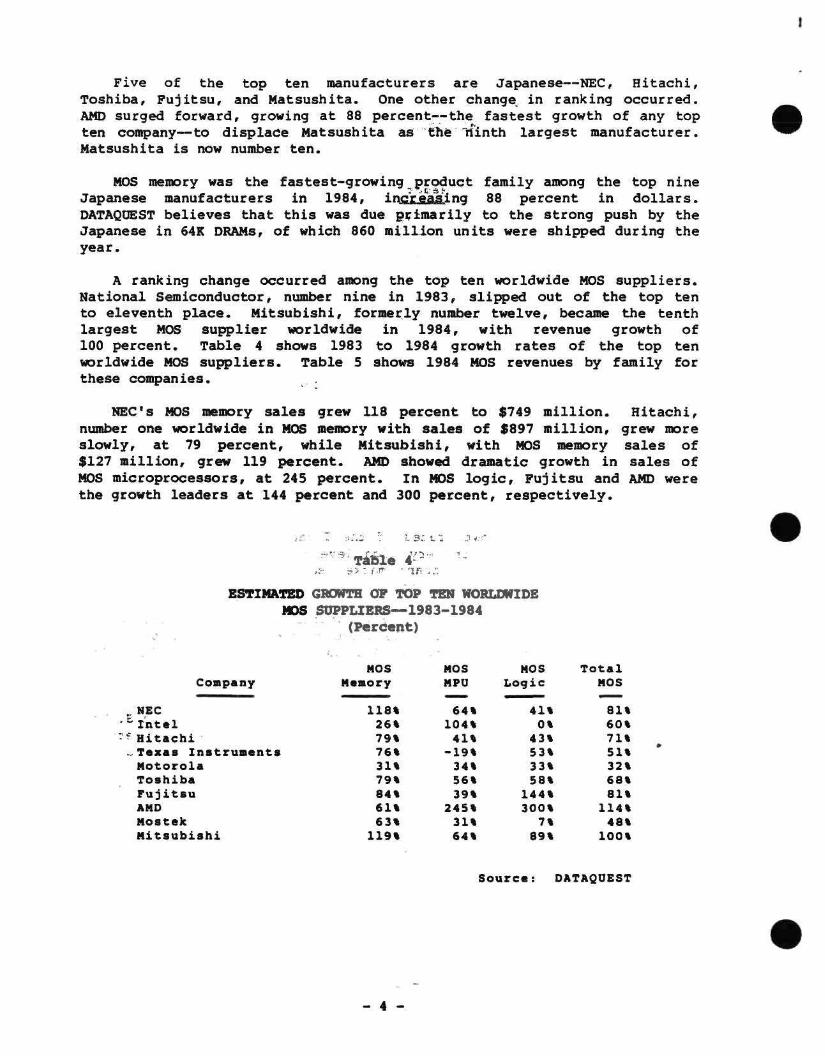
Five of the top ten manufacturers are Japanese—NEC, Hitachi, Toshiba, Fujitsu, and Matsushita. One other change in ranking occurred. AMD surged forward, growing at 88 percent—the fastest growth of any top ten company—to displace Matsushita as th6 tiinth largest manufacturer. Matsushita is now number ten.
MOS memory was the fastest-growing product family among the top nine Japanese manufacturers in 1984, injZJLSaiLing 88 percent in dollars. DATAQOEST believes that this was due primarily to the strong push by the Japanese in 64K DRAHs, of which 860 million units were shipped during the year.
A ranking change occurred among the top ten worldwide MOS suppliers. National Semiconductor, number nine in 1983, slipped out of the top ten to eleventh place. Mitsubishi, formerly number twelve, became the tenth largest MOS supplier worldwide in 1984, with revenue growth of 100 percent. Table 4 shows 1983 to 1984 growth rates of the top ten worldwide MOS suppliers. Table 5 shows 1984 MOS revenues by family for these companies.
NEC's MOS memory sales grew 118 percent to $749 million. Hitachi, number one vrorldwide in MOS memory with sales of $897 million, grew more slowly, at 79 percent, while Mitsubishi, with MOS memory sales of $127 million, grew 119 percent. AMD showed dramatic growth in sales of MOS microprocessors, at 245 percent. In MOS logic, Fujitsu and AMD were the growth leaders at 144 percent and 300 percent, respectively.
.^f .. rs;.i T i-s: t;; .3 <';"
^ Til5l6 4 "
ESTIMATED GROWTH OF TOP TEN WORLDfflDE MOS SUPPLIESS—1983-1984
(Percent)
Company
NEC Intel Hitachi Texas Instruments Motorola Toshiba Fujitsu AMD Hostek Mitsubishi
MOS Memory
118% 26% 79% 76% 31% 79% 84% 61% 63%
119%
MOS HPU
64% 104% 41%
-19% 34% 56% 39%
24S% 31% 64%
MOS Logic
41% 0%
43% 53% 33% 58%
144% 300%
7% 89%
Total MOS
81% 60% 71% 51% 32% 68% 81%
114% 48%
100%
Source: DATAQOEST
- 4 -
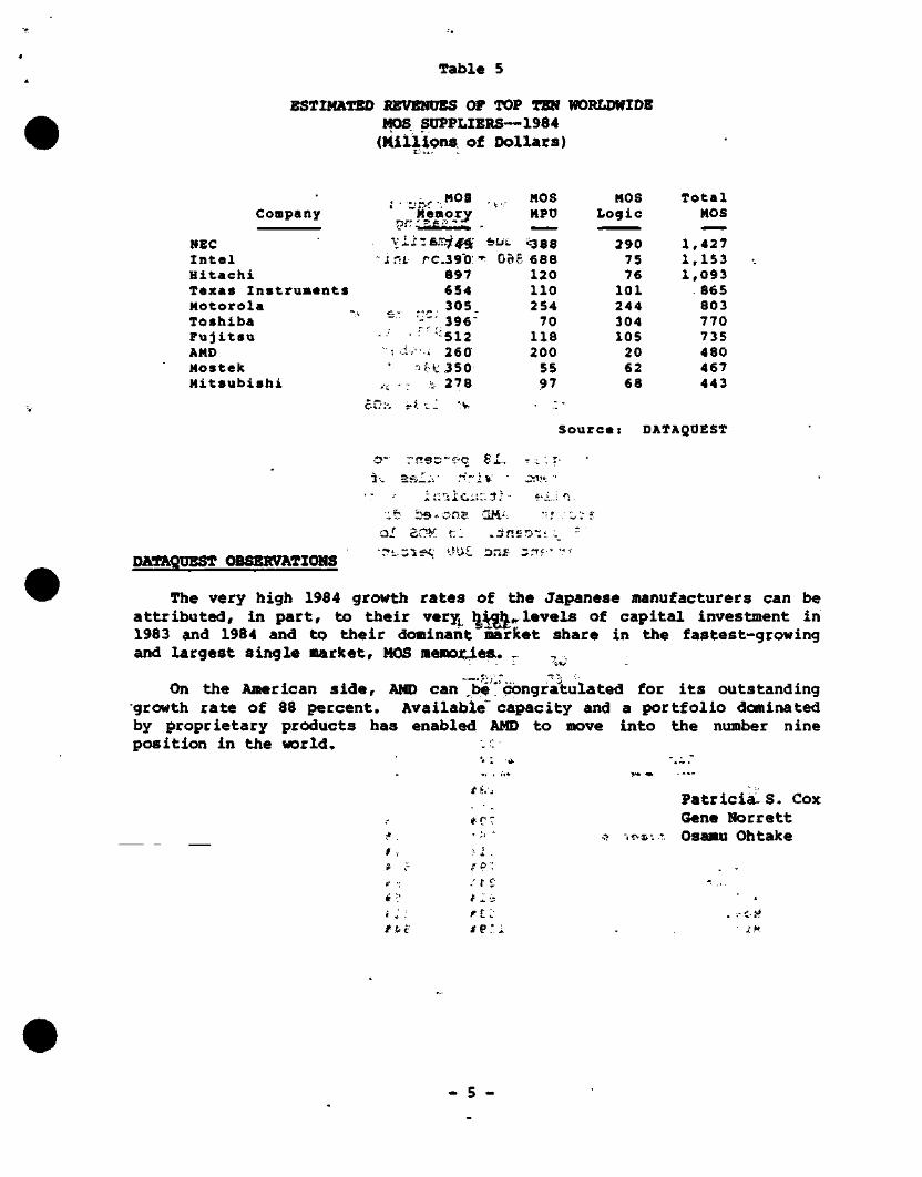
Table 5
ESTIMATED HEVENDES OF TOP TEN WORLDWIDE HOS StJPPLIERS—1984 (HilllQns Of Dollars)
Company
NEC Intel Hitachi Texas Instruments Motorola Toshiba Fujitsu AMD Mostek Mitsubishi
. . ; ^ . HOS "Memory
pr^^&j^;::; . . \lx-:Btri4^
• % • • •
BUL
~ mv re.39."0:' 0o6 897 654
c .- 3°5. - - 396"
.• ,''f-5j_2
•-;.i/';.i 2 6 0 •if-fe350:
.c ?i 2 7 8
NOS MPO
^ 8 8 688 120 110 254 70
118 200 S5 97
MOS Logic
290 75 76
101 244 304 105 20 62 68
To ta l MOS
1 1 1
.427 ,153 ,093 865 803 770 735 480 467 443
DATAQPEST OBSEBVATIONS
aC-.'. r-i. i
3 - r n e c - € f c 8 1 . «iV V. 2 t i £ , i - r<r'i% ' •SV':
i n ^ i i c i i - : ? ; - « i :.b b « » c n B QM.--. ••!
al SDK v.: . .J.nsDi-. • ."•t .-1st 'J'.)£. Daf. 2n?- '
Source: DATAQUEST
The very high 1984 growth rates of the Japanese manufacturers can be attributed, in part, to their very^ t| h,,rlevels of capital investment in 1983 and 1984 and to their dominant "market share in the fastest-growing and largest single market, MOS memQJc4es. -
' -. 1 -'i-tj
On the American side, AMD can ,be' congratulated for its outstanding growth rate of 88 percent. Available" capacity and a portfolio dominated by proprietary products has enabled AMD to move into the number nine position in the world.
Patricia. S. Cox tr-~ Gene Norrett
* • ?'' ^ i as'r Osamu Ohtake f = ii. * ,'- fp"- . .
i J • f t J . 1- i- i^
f t - c <fe.:i. - - if
- 5 -


