Embed Size (px)
Citation preview

Ref. p. 74] 3.8.2 H2O and OH on semiconductors 1
Landolt-Börnstein New Series III/42A4
3.8.2 H2O and OH on semiconductors
W. JAEGERMANN, TH. MAYER
3.8.2.1 Introduction
In this data collection the adsorption and adsorbate properties of H2O and OH on well defined semiconductor surfaces in UHV are summarized. The adsorbate induced changes of substrate properties are only considered, if they are intrinsically related to the adsorption process. They are subjects of other parts of this LANDOLT-BÖRNSTEIN III/42A2. Here only those effects are mentioned which are absolutely necessary to understand the basic adsorbate properties. Reactions with the substrate are only covered, if they are immediately connected with dissociative adsorption below or at room temperature. Thermally induced reactions at elevated temperatures, usually an oxidation of the semiconductor substrate and details about the involved mechanisms, are not presented here in any detail, despite the fact that many papers dealing with H2O adsorption are motivated by this process and contain results in this respect. A number of review articles have been published in the past, which present and discuss the interaction of H2O with semiconductor surfaces (see e. g. [87F, 88F, 95W1]).
The interaction of H2O with semiconductor surfaces is studied to achieve a fundamental understanding of solid/liquid interfaces involving aqueous solutions. Such interfaces are the essential part of semiconductor based devices as (photo)electrochemical and (photo)catalytic cells and sensors. They are also of central importance in wet chemical etching and processing steps in semiconductor microelectronics as e.g. in passivating oxide formation. Usually the number of reactants is rather large in these applications and the interface interactions may become very complex. As a consequence the electronic properties of the interfaces may vary depending on the processing steps strongly influencing the operation of the devices. In many cases the microscopic origin of the involved changes are not very well understood, as the species interacting with the semiconductor surfaces have not been identified and their electronic interactions remain unclear. As H2O is often the main constituent with high surplus in the solution its interaction with the semiconductor must be understood in very detail. Thus, H2O as an adsorbate on defined semiconductor surfaces is of basic interest and also a key ingredient to a fundamental understanding of wet-chemical processes in many technological applications.
In contrast to metals the bonding interactions of semiconductors are governed by localized and directional chemical bonds. Therefore the adsorption process as well as the adsorbate properties are in general strongly influenced by the structure and chemical composition of the substrate surface, which again depends on the preparation procedure used for a specific semiconductor [92B, 95M]. The atomic structure of semiconductor surfaces deviate considerably from bulk truncated surfaces as most semiconductors undergo severe surface relaxations and reconstructions to minimize their specific surface energies. Thermodynamic driving force is the attempt to minimize the number of energetically unfavourable surface dangling bonds produced by the loss of translational symmetry across the surface. Furthermore compound semiconductors exhibit surface atoms of different polarity adding electrostatic potentials and different dangling bond energies to the surface energy. As a consequence the adsorption is strongly dependent on the specific surface orientation and the kind of semiconductor used for investigation. In addition, the procedure of surface preparation and the obtained defect concentration may vary in different investigations which also influences the adsorption process. Therefore the data and conclusions given in literature may differ due to these effects. These factors will be discussed in more detail in section 3.8.2.2 and 3.8.2.3. Different surface terminations imply very different surface electronic structures ([92B, 94H, 94S2, 95M] and LANDOLT-BÖRNSTEIN III/24B, chapter 3.2 by Calandra and Manghi). Already on clean semiconductor surfaces the energetic position and dispersion of surface states and surface resonances strongly influences the charge distribution between semiconductor bulk and surface. Local dipoles involve only the surface atoms, but extended space charge layers lead to extended layers of ionized dopants in the bulk. As the adsorption of H2O as an electron donating adsorbate induces charge transfer from its occupied molecular orbitals to the semiconductor, the electronic structure of the surface changes with adsorption. On the other hand a dissociative adsorption will lead to surface bound OH and H groups
2 3.8.2 H2O and OH on semiconductors [Ref. p. 74
Landolt-Börnstein New Series III/42A4
which may be neutral or partially negatively/positively charged. Depending on their bonding properties and surface molecule energy states the charge transfer between the bulk and the surface may change again. As a result adsorbed H2O or OH and H may strongly change the electronic surface potentials and, vice versa, the given surface potentials of the semiconductor substrate controlled by its doping may influence the adsorption process. A more detailed discussion on these effects is given in section 3.8.2.4.
The variation in structural and electronic properties of different semiconductors with their specific surface terminations leads to strongly varying adsorption properties and bonding interactions. The interaction with adsorbates as H2O and its dissociation products will depend on the number, distances and relative orientations of specific surface atoms and related bonding sites. Due to adsorption the substrate structure and electronic structure will change again in most cases. It turns out that depending on the experimental conditions as e.g. temperature and dosage the exposure of most semiconductors to H2O does not only lead to adsorption but the adsorbate species may further react with surface and subsurface atoms. These surface reactions following the adsorption step lead to oxidation and etching, which may already be initiated at low sample temperatures. Therefore, it is hardly possible to prepare identical adsorption stages in different experiments. Many contrary interpretations on H2O adsorption on semiconductors are probably related to this effect that adsorption and subsequent reaction steps occur in parallel. Most of the work on water adsorption on semiconductors has been performed with Si surfaces. This is evidently in part motivated by the fact that Si is the best established semiconductor material, which can rather easily be prepared in different surface orientations and defined reconstructions. In addition, it is the semiconductor most important in technology. Especially the interaction with H2O is of interest for etching processes, the formation of H-terminated surfaces, and oxide growth. A large number of investigations have been performed using different surface science techniques. For the technically important Si(100) surface and to a lesser extent for the Si(111) surface the interaction of H2O (OH) as an adsorbate is well studied and reasonably well understood. In cases where some uncertainties may still exist these are given in the text and added as remarks in the tables. For all other semiconductors the number of investigations is much smaller. In these cases there is no general agreement on H2O adsorption, yet. Even the most simple question on the mode of adsorption – dissociative or molecular – is still not clarified for many semiconductors. For these semiconductor substrates it is attempted to give a survey of the performed experiments and the main conclusions, as given in the original contributions. We do not attempt to draw any final conclusions on the mode of adsorption and the adsorbate properties. In cases, where parts of the results seem to be questionable based on other and more recent investigations, remarks will be added in the text and as a comment in the tables.
List of Acronyms and Symbols used in this chapter
Acronyms AES Auger electron spectroscopy ARUPS angle resolved UPS CNDO complete neglect of differential overlap of atomic orbitals on the same atom DB dangling bond DAS dimer adatom stacking fault DFT density funtional theory ELS energy loss spectroscopy EHT extended Hückel theory ESDIAD electron stimulated desorption ion angular distributions HREELS high resolution electron energy loss spectra IR infrared IRAS infrared absorption spectroscopy LCAO linear combination of atomic orbitals LDA local density approximation LDFT local density functional theory LDFT/LDA LDFT within the local density approximation

Ref. p. 74] 3.8.2 H2O and OH on semiconductors 3
Landolt-Börnstein New Series III/42A4
LEED low energy electron diffraction LEIS low energy ion scattering LITD laser induced thermal desorption MNDO modified neglect of diatomic overlap MO molecular orbital ODA outer dimer atom PED photo electron diffraction PSID photon stimulated ion desorption PYS photoemission yield spectroscopy SIMS secondary ion mass spectrometry STM scanning tunneling microscopy SXPS soft XPS or synchrotron induced XPS TDS thermal desorption spectroscopy TPD thermal or temperature programmed desorption TOF-SARS time of flight scattering and recoiling spectrometry UHV ultra high vacuum UPS ultraviolet photoelectron emission spectroscopy XPS x-ray photoelectron emission spectroscopy Symbols ∆φ change of workfunction χ electron affinity ∆χ change of surface dipol ∆EB change of binding energy EB binding energy EB
F binding energy referenced to EF EB
vac binding energy referenced to vacuum level EB
VBM binding energy referenced to valence band maximum EF Fermi level Evac vacuum level eVbb band bending EVBM valence band maximum θ coverage θ/θsat relative coverage θsat saturation coverage Hads adsorbed hydrogen L exposure to adsorbate (H2O) in Langmuir 1 × 10⁻⁶Torr × 1s ML monolayer Oads adsorbed oxigen OHads adsorbed OH RT room temperature Siad adatom of Si(111)7×7 reconstruction Sirest restatom of Si(111)7×7 reconstruction S sticking coefficient S0 initial sticking coefficient for θ →0 S/S0 relative sticking coefficient 100 K sample temperature in K →300 K adsorption at low temperature, measurement taken after annealing to 300 K

4 3.8.2 H2O and OH on semiconductors [Ref. p. 74
Landolt-Börnstein New Series III/42A4
3.8.2.2 Surface preparation
The adsorption of H2O on semiconductor surfaces evidently depends on the type of semiconductor, its surface orientation, and the procedure applied to prepare clean and defined substrate surfaces. For this reason some early experiments on H2O adsorption on powdered/crushed semiconductors published in the literature will not be considered in this data collection (see e.g. [68E]). The different techniques known for the preparation of metal surfaces in UHV, namely thermal cleaning, ion bombardment, ion bombardment and annealing, and in situ deposition by any vacuum deposition process cannot be applied with the same success to most semiconductor surfaces. The different surface orientations of elementary semiconductors like Si and Ge are usually prepared by cleaving in vacuo or by ion bombardment and annealing. Also starting from chemically etched surfaces is possible, which is followed by a thermal cleaning process. In general, there are well established procedures available, which allow to prepare surfaces of comparable quality.
For compound semiconductors the surface preparation may be very complex depending on the specific surface orientation under consideration. High quality substrate surfaces are obtained for the cleavage planes, which are the non-polar surfaces of the substrate material. For compound semiconductors with Zinkblende structure as e.g. GaAs these are the (110) planes. All other surface orientations are usually prepared by several ion bombardment and annealing cycles, which may result in many different surface reconstructions or facetting. In principle, it is also possible to obtain high quality surfaces of most surface orientations by in-situ MBE growth or by transferring epitaxial films from any growth chamber using shielding surface layers, which can be heated off at elevated temperatures. To our knowledge such surfaces have hardly been used for the investigation of H2O adsorption. Therefore, adsorption studies on compound semiconductors suffer from different surface pre-treatments and for this reason from differing surface properties.
High quality defect free and chemically inert substrate surfaces can be prepared from the (0001) van der Waals cleavage plane of layered chalkogenide semiconductors. The chemically saturated hexagonally closed packed cleavage plane allows physisorption of H2O at low sample temperatures only.
Some general information on preparation methods used for the different semiconductor surfaces can be found in the following references [83K1, 92B, 95L, 95M], see also LANDOLT-BÖRNSTEIN III/24A. Details on the preparation of the substrates are usually given in the experimental part of the cited papers.
3.8.2.3 Surface structure: relaxation and reconstruction
Clean semiconductor surfaces of a defined crystallographic plane do usually not exist in their bulk truncated structure. Assuming homonuclear cleavage of bonds in surface formation unsaturated directional dangling bonds are formed which are only occupied with a single electron. In order to minimize the surface free energy these semiconductor surfaces exhibit a pronounced tendency to surface relaxation or reconstruction, which may involve a severe structural rearrangement of surface atoms. Thermodynamic driving force is the reduction of the number of energetically unfavourable dangling bonds and/or of their electronic character by charge redistribution. Whereas relaxation processes and also some surface reconstructions can occur spontaneously, some of the thermodynamically more stable surface reconstructions need the thermal activated diffusion of surface atoms. Therefore, the structural rearrangement on the idealized surface is also influenced by the substrate temperature profile used within the preparation sequence. As a consequence different surface terminations are known to exist for elementary and compound semiconductors depending on the preparation sequence used, which are listed in several reviews [83K1, 92B, 95L, 95M] and a previous LANDOLT-BÖRNSTEIN III/24A. The reader should refer to this article for the representation of the structural arrangement of a certain surface, given in the established notation of its superstructure as e.g. found in LEED. The number of dangling bonds, their distance and orientation to each other, as well as their atomic origin deviate considerably on the different semiconductor surfaces. As these dangling bonds act as adsorption sites one expects strong variations in H2O adsorption properties on different semiconductor surfaces.

Ref. p. 74] 3.8.2 H2O and OH on semiconductors 5
Landolt-Börnstein New Series III/42A4
The semiconductor substrates considered in this review are: • the elementary semiconductor surfaces Si(100), Si(100)2×1, Si(100)2×1 vicinal, Si(111)7×7,
Si(111)2×1, Si(113)3×1, Si(113)3×2, Ge(100)2×8, Ge(100)2×1, Ge(111)2×8, GexSi1-x(100)2×1; • the 3-5 compound semiconductor surfaces GaAs(100), GaAs(100)2×4, GaAs(100)4×6, GaAs(110),
InP(110), InP( 111_
), AlAs(100)1×1; • the chalcogenide semiconductor surfaces GaSe(0001), InSe(0001), MoSe2(0001), MoS2(0001),
WSe2(0001); pyrite FeS2(100); • and the ternary compound semiconductor surface CuInSe2(011)
Furthermore, the adsorption also is influenced by the ideality (structural quality) of the prepared surface. The number of defects depends on the detailed experimental procedure used for the preparation. The experimentally observed results may be governed by these defects, which may act as adsorption and dissociation sites on otherwise inert surfaces. For more complex surface terminations the „intrinsic“ adsorption properties of a specific surface orientation can hardly be discerned, if the number of defects after preparation is large. But the number of defects, which are actually obtained, are hardly known for most investigations (besides when using techniques like STM) and are usually not quantified. A summary of possibly formed defects on semiconductor surfaces is also given in LANDOLT-BÖRNSTEIN III/24A, chapter 2.3 by Henzler and Ranke.
3.8.2.4 Surface electronic structure and surface potentials
The electronic structure of different semiconductor surfaces may also vary depending on the type of semiconductor surface and the existing reconstruction. The energy levels of dangling bonds formed on the surface may be situated in the bulk bandgap forming surface states or may be outside the gap forming surface resonances. As a consequence the semiconductor substrate has different surface electronic properties. In some cases e.g. with Si(111)7×7 the surface is metallic; in other cases e.g. for the perfect GaAs(110) cleavage plane a semiconducting surface is found without electronic states in the bandgap. Also the charge carried by different surface atoms may be different. This is evident for compound semiconductors: on GaAs(110) the surface relaxation is accompanied by a partial electron transfer from Ga to As dangling bonds. But also for elementary semiconductors differently charged surface atoms exist: On the Si(100)2×1 surface the outer dimer atom is negatively charged whereas the inner dimer atom is positively charged. On Si(111)7×7 the adatoms are positively charged whereas the neighboring rest atoms are negatively charged. Polar surfaces as e.g. GaAs (100) or (111) are usually strongly reconstructed with a surface excess of one atomic species, which then dominates the surface electronic structure. Thus, one may expect the adsorption of H2O as nucleophylic species and subsequent dissociation to occur on different surface sites. The reader should refer to [88H, 94H, 94S2, 95M] and LANDOLT-BÖRNSTEIN, III/24B, chapter 3.2, where the electronic surface properties of clean semiconductor surfaces have been summarized in very detail. It should be noted at this stage that similar to the structural properties of semiconductor surfaces also the electronic properties depend very much on the quality of surface preparation. Defects or contaminations may introduce extra surface states and surface resonances, which do not exist on the perfect surface. The energetic positions of the semiconductor band edges in reference to the vacuum level are given by the values of the ionization potential Ip = (Evac – EVB) and electron affinity χ = (Evac – ECB) of a specific semiconductor surface. For different surface orientations these values only depend on changes of the localized surface dipole extending about a few monolayers. This surface dipole is determined by the polarity of the surface bonds. The surface position of the Fermi level in reference to the semiconductor band edges and thus the work function φ = (Evac – EF) additionally depends on the relative position of the bulk Fermi level and the energetic level and occupation of surface states [95M, 96J]. The bulk Fermi level

6 3.8.2 H2O and OH on semiconductors [Ref. p. 74
Landolt-Börnstein New Series III/42A4
is given by the type of doping states (acceptor states: p-type; donor states: n-type) and their concentrations. Flat band conditions, which correspond to the lack of extended space charge layers, can only be expected for surfaces free of surface states. In this case the work function of a p-doped semiconductor is larger than that of an n-doped one by the difference of the bulk Fermi level positions. Active surface states may lead to band bending eVbb in the surface region of the semiconductor typically in the range of 100 to 104 Å (inverse proportional to bulk doping). Vice versa the work function is changed by the shift of the Fermi level given by eVbb versus the band edges. Acceptor (donor) like surface states will accept (donate) electrons from (to) the bulk of the semiconductor, if their energy position is below (above) the bulk Fermi level. For high concentrations of surface states the surface Fermi level is pinned at the energetic level of the surface states; as a consequence p- and n-doped semiconductors show the same work function. The electronic properties of clean semiconductor surfaces are summarized in Ref. [88H, 94H, 94S2, 95M] and LANDOLT-BÖRNSTEIN III/24A, chapter 3.2. With adsorption and depending on the bonding properties the electronic surface states or resonances may change their character (acceptor or donor) and/or energy position in respect to the band edges. As a consequence the band bending and surface dipole will usually be changed.
The value of the binding energy EB of electronic states measured e.g. for adsorbed species by photoemission depends on the reference level used. If the Fermi level is used as common reference level (EB
F) a shift of binding energy value may occur with adsorption, which is related to a change of semiconductor band bending corresponding to a surface Fermi level shift. This band bending can be related to a charge transfer from the bulk to the adsorbate or may be induced by the adsorbate due to passivation of electronically active surface states originally present in the bulk bandgap of the material. As a consequence the binding energy values EB
F may change with coverage without any change in the adsorbate electronic state. The induced band bending will also influence the changes of the work function ∆φ = eVbb + ∆χ; with ∆χ as the change in electron affinity due to changed surface dipole potentials. To avoid changes due to band bending the binding energy values are also referred to the valence band maximum EVBM. In this case only surface dipole potentials showing up between the adsorbate and the substrate may shift the relative binding energy values of adsorbate vs. substrate lines. If the vacuum level is taken as reference level, the binding energy values EB
vac are affected by band bending eVbb and surface dipoles [95M, 96J] e.g. by the overall shift of work function ∆φ. The changes of surface potentials are not specifically covered in this part of the LANDOLT-BÖRNSTEIN series on adsorption but in the contribution of Jacoby and Nilsson et al. (LANDOLT-BÖRNSTEIN III/42A2, chapters 4.2 and 4.3). But for presenting the electronic properties of adsorbate states the different reference values and their influence on the experimentally determined binding energy values always have to be kept in mind. In principle, the different binding energy scales can be referred to each other, but, unfortunately, the necessary data on band bending and work functions are not given in all papers presented in this work.
One may also expect a strong influence of semiconductor bulk doping on H2O adsorption. If charge transfer from the bulk to the adsorbate is involved, the type of doping and the related band bending defines, which type of charge carrier, electron or hole, is more easily available in the adsorption process. This has been extensively discussed in older work on ionosorption (ionic adsorption) of adsorbates on oxide semiconductors [55H, 63W, 77M], but has not been studied in any detail in more modern work with defined semiconductor surfaces. As in many cases even the doping of the semiconductors are not given in the cited papers, we did not specifically address this point in this data summary.
3.8.2.5 Methods of investigation
For the investigation of H2O adsorption on semiconductor surfaces all relevant techniques of surface science have been applied during the last years. Only experiments performed in UHV have been considered thus excluding e.g. scanning probe experiments at air or in solutions. The principles of the most important methods of investigations are described in detail in LANDOLT-BÖRNSTEIN III 42/IA2. chapter 2. General information on experimental techniques can also be found in other LANDOLT-BÖRNSTEIN volumes as III/24 and in many monographies on surface science techniques. We use the standard abbreviations without further explanations. They are summarized in section 3.8.2.1. Also theoretical calculations using different methods were applied. For details and limitations the reader may refer to the original literature.

Ref. p. 74] 3.8.2 H2O and OH on semiconductors 7
Landolt-Börnstein New Series III/42A4
We also want to note that the application of a certain technique may disturb the adsorption process and the obtained results. In general, the degree of disturbance decreases from ions to electrons to photons, and also from high energies to small energies. Especially with semiconductors the formation of defects may already be introduced by the use of high energy photon beams of high brilliance as e.g. given by synchrotron radiation. These effects may be even more severe, if adsorbates are present. It is usually expected that spectroscopic techniques as UPS and IR do not disturb or modify the surfaces. But in any case changes of spectral features with time may indicate probe induced surface processes. Also the thermal excitation of the adsorbate by hot filaments must be taken into account. For well defined experiments pressure measurements are performed in clear separation from the substrate. This could not be verified for all of the quoted experiments. A discussion on probe induced modification of the adsorption process was part of the controversy on molecular and dissociative H2O adsorption on Si surfaces.
3.8.2.6 Adsorption mode
For all semiconductors and their different surface terminations there was a long lasting controversial discussion in literature, if the mode of H2O adsorption is dissociative or molecular. This controversy seems to be settled now at least for Si(100), Si(111), and Ge, for which the experimental results clearly support dissociative adsorption at room temperature saturating the surface dangling bonds (see Table 1). On Si even at low temperatures dissociation occurs. On top of the dissociative adsorption layer molecular H2O may be condensed as H-bonded physisorbed ice layer, at substrate temperatures below 150 K. At elevated temperatures above RT the oxidation of the surface sets in after complete dissociation of H2O into Oads and 2Hads. This process is (at least partly) already observed at RT or even below.
The adsorption mode of H2O on 3-5 semiconductors seems to be less clear. Some data suggest an initial dissociative adsorption even at low temperature, whereas others support a dissociative adsorption only at RT and some authors conclude on strongly chemisorbed H2O (Table 1). The reactivity may also depend on the surface orientation and the applied preparation conditions. The orientation dependence of H2O adsorption on 3-5 semiconductors has not been systematically studied, yet.
The layered chalcogenides with their chemically inert van der Waals (0001) surfaces seem to be the only system identified so far, for which physisorbed H2O (ice layer) is condensed at low temperatures (<150 K). It is completely desorbed without dissociation above this temperature.
We do not include in Table 1 results from theoretical calculation as they are only significant in comparison to experimental results (see Table 2 and 6).
Si (100) and its reconstructions
All the earlier investigations were mainly addressed to the question whether water adsorption on Si surfaces is either molecular or dissociative. According to ellipsometry data, it was proposed [71M] that H2O dissociates into 2H and O to saturate all the surface dangling bonds. Early UV photoemission spectra were interpreted to be due to molecular adsorption [81F1, 81F2, 83S2] but could not be confirmed later on. UPS measurements performed later give different spectra [83S2, 84O, 89F], which now are attributed to OH and H groups saturating the Si(100)2×1 dangling bonds. HREELS and IR spectra clearly prove dissociative chemisorption forming Si-OH and Si-H surface molecules [82I2, 84C2]. There is now general agreement that the dominating process below about 400 K is dissociation into OH and H species which saturate two dangling bonds (DBs) of the 2×1 reconstructed surface (Fig. 1, Fig. 12). STM work [93A, 93C2] shows that the reconstructed dimer bonds of the substrate are not broken which was also concluded from the LEED observation of retaining the (2×1) superstructure [82I2, 84S1, 85C, 87L2]. At low temperatures (below 140 K) molecular water may be condensed on top of the dissociated layer. Above 400 K chemisorbed OH species begin to react further forming atomically adsorbed oxygen [96R2, 97W].

8 3.8.2 H2O and OH on semiconductors [Ref. p. 74
Landolt-Börnstein New Series III/42A4
Si (111) and its reconstructions
There is now general agreement that on Si(111)7×7 adsorbed H2O initially dissociates into OH and H adsorbate species even at about 80 - 90 K, which saturate two neighboring adatom-restatom pairs in the DAS model of the 7×7 surface reconstruction. This conclusion is now consistently supported by HREELS [82I2, 83K1, 85N, 86N, 86S2], UPS [89F], SXPS [95P] and STM [91A, 97S1] data. Early UPS experiments [79F, 81F1, 81F2] were never reproduced in this way and the observed spectra are probably due to the onset of oxidation. Later UPS results [85R1, 85R2, 86S2] show spectra dominated by OHads due to dissociatively adsorbed H2O, which have been misinterpreted. Depending on coverage and temperature different dangling bond states are involved leading to different stages of adsorption in the range of about 0.12 and 0.19 ML. It is suggested that OH occupies the adatom sites and H the restatom sites [91A, 97S2], but theoretical calculations also propose a reverse occupation of bonding sites [97E]. The energy and angle dependencies of the vibrational modes in HREELS indicate a preferential orientation of the Si-OH and Si-H bond nearly normal to the surface and of the SiO-H bond tilted by 75° from the surface normal [86N]. The 7×7 reconstruction remains unchanged during the initial adsorption process. At room temperatures and high exposures a slow saturation of all surface dangling bonds is found and subsequently a thermally activated reaction with Si back bonds and complete dissociation into Oads and 2Hads is evident. At this stage the surface reconstruction is lost and the oxidation of Si sets in [85N, 85R1, 89K, 95P, 96F, 97S1].
The adsorption of H2O on laser annealed Si(111)1×1 surfaces also leads to a dissociative adsorption in a much higher surface concentration, which is related to the increased number of surface dangling bonds on this surface [95W2].
The adsorption mode on Si(111)2×1 is less clear. Also here a dissociative adsorption is experimentally found, which is accompanied by a loss of the π−bonded chain structure [84S1].
Ge in different surface orientations
H2O is suggested to be molecularly adsorbed on Ge(100)2×1 and Ge(111)2×8 surfaces at low temperatures (110 K) or as mixture of dissociative and molecular adsorption. [84C1, 87K1, 87K2, 89L, 91L1, 91L2, 91P1, 92C, 93R1, 93R2]. At RT dissociative adsorption is found for all orientations. The OHads and Hads species saturate the surface dangling bonds available at the surfaces. The surface reconstruction is lost due to adsorption as deduced from the loss of superstructure diffraction spots in LEED. At elevated temperatures the surface is at least partly oxidized [87K3, 91P1].
3-5 semiconductors in different surface orientations
Only a small number of H2O adsorption studies with 3-5 semiconductors have been performed so far and no conclusive results on the mode of adsorption for different compounds and surface orientations can be given up till now. Adsorption studies have been performed either with the unreconstructed but relaxed (110)1×1 cleavage plane or with the reconstructed (100) and (111) planes. Based on SXPS data some authors have suggested an initial dissociative adsorption even at low temperatures on (110) surfaces forming Ga(In)-OH and As(P)-H pairs in correspondence to the related Si and Ge surfaces [96H, 97H, 00H]. Others suggest physisorbed and chemisorbed molecular adsorption but the obtained UPS spectra do not agree to the expected emission pattern observed later on other substrates [79B]. On (100) surfaces molecular adsorption is suggested at low temperatures, which is followed by thermally activated dissociation [97M1, 97M2, 98C]. Dissociation always leads to the formation of group 3-OH and group 5-H bonds as the group 5-OH and group 3-H bonds are thermodynamically unfavorable. In all cases the long range surface structure as given by LEED remains unchanged during initial adsorption.

Ref. p. 74] 3.8.2 H2O and OH on semiconductors 9
Landolt-Börnstein New Series III/42A4
Miscellaneous semiconductors
The van der Waals (0001) surfaces of layered chalcogenides are composed of a close packed array of chemically saturated chalkogenide surface atoms free of dangling bonds. Thus H2O is only adsorbed molecularly as condensed ice layer at low temperatures (< 150 K) and is completely desorbed at temperatures above. No oxidation is found despite on step edges. For FeS2 (100) and CuInSe2 (011) at low temperatures a preferential adsorption of molecular H2O is suggested on Fe and Cu sites, respectively. The stable molecular adsorption was related to the coordination type bonding to transition metal sites.
3.8.2.7 Thermodynamic data of adsorption
There are no recent attempts published to measure thermodynamic data quantitatively e.g. in calorimetric experiments (adsorption isotherms), due to the thermal activated reactivity of most semiconductors with the adsorbate species H2O and OH. Older data as given in [68E] suffer from an insufficient characterization of the surface structure and composition. Informations on adsorption energies are thus only available from kinetic experiments. But also in such studies the determined activation energies on desorption may be affected by the parallel process of thermally activated reactions of the chemisorbed species with the semiconductor substrates (oxidation). At elevated temperatures most semiconductors form oxides before the chemisorbed adsorbates (H2O and OH) desorb. Only for multilayer coverage (ice formation) at low temperatures the physisorbed layers will be desorbed at typical temperatures above 150 K. Data on adsorption energies are also available from theoretical calculations, which give bonding energies as calculated for isolated adsorbate/substrate surface molecules. As an example, on the Si(100)2×1 surface dissociation is observed even at low temperatures (80 - 100 K) [84C2, 85R1] indicating that a possible activation barrier, if existing at all, is quite low. Engler used a theoretical calculation (empirical potential method) to argue that the energy difference between molecular and dissociative adsorption is small, though he predicted a large activation barrier between these states [90E]. In an LDA-DFT calculation the enthalpy change accompanying dissociative chemisorption of one H2O molecule was calculated to be 3.9 eV [95V].
Using other DFT calculations and cluster models of the surface the energy and mechanism of adsorption, the stability of the dissociated products, and the minimum energy reaction path (Fig. 1) were calculated by Konecny et al. [97K]. In agreement with experimental data they found evidence for a weakly bound molecular precursor but no net activation barrier for adsorption. The values given for the adsorption energy from the different applied methods are summarized in Table 2.
3.8.2.8 Kinetic data of adsorption/desorption, surface diffusion and surface reactions
The kinetics of adsorption are usually determined by the relative sticking coefficient S/So (So: sticking coefficient for θ → 0) versus relative coverage θ/θsat. (θsat: saturation coverage). These curves are derived from adsorbate coverages versus exposure. For all well studied semiconductors the experimentally observed sticking coefficients and saturation surface coverages depend strongly on the experimental conditions as surface orientation, temperature, and pressure regime. The changes in relative adsorbate coverage for different surface orientations have been clearly demonstrated with cylindrical single crystals of Si [85R3] (Fig. 2a) or Ge [87K3] (Fig. 9) or with lensshaped samples of Si [90S]. The shape of the adsorption curves cannot be explained by Langmuir adsorption, but are typical for an adsorption process with a mobile precursor state [96R3] as treated by Kisliuk [57K, 58K]. In this model impinging molecules may migrate both over occupied and unoccupied regions of the surface and are finally chemisorbed on two adjacent unoccupied dangling bond sites. It is now well accepted that for the most often studied semiconductor surfaces of Si and Ge initially a fast and nearly activation free dissociative adsorption occurs on bonding sites in close neighborhood to each other. Subsequently, substrate surface bonds are attacked in a thermally activated process, which is accompanied by further adsorption of additional H2O
10 3.8.2 H2O and OH on semiconductors [Ref. p. 74
Landolt-Börnstein New Series III/42A4
molecules. This process is related to the disruption of reconstruction bonds and back bonds. Thus, the adsorption kinetics depend on the number and distances of specific dangling bonds as given by the surface reconstruction of the semiconductor surface.
There are no data available on the desorption kinetics of adsorbed H2O and OH besides the desorption of condensed ice layers covering the first adsorbate layer. This is due to the fact that after dissociative adsorption of H2O the surface species react in a thermally activated process with semiconductor substrate atoms to form oxides, which involves the complete dissociation of H2O with the intermediate step to OHads and Hads and finally to Oads and 2Hads. Thus, in thermal desorption spectra first the desorption of H2 is observed at elevated temperatures which is followed by the desorption of SOx species (S = surface atom). H2O adsorption studies on semiconductor surfaces and subsequent activated formation of oxides is motivated by the interest in understanding the basic processes involved in the high temperature wet-oxidation of semiconductors used in electronic device processing. Detailed studies on the thermally activated wet oxidation following adsorption of H2O is found for example in the following papers (Si: [85N, 89K, 96F] Ge: [87K3, 91P1] 3-5: [93C1, 96H, 97M1, 98C, 00H]). In this data collection the substrate oxidation is considered only if it occurs in adsorption/desorption experiments of adsorbed H2O or of the dissociation product OH, but not as a subject in itself.
The results obtained on kinetic aspects of adsorption and desorption as well as surface diffusion and reaction are summarized in Table 3.
Si (100) and its reconstructions
The kinetics of adsorption has been investigated in detail in the temperature range from below 140 K, where multilayer adsorption becomes possible, to above 400 K, where OH radicals begin to react further eventually forming atomically adsorbed oxygen [96R2, 97W].
STM work [93A, 93C2] shows that the reconstruction dimers of the substrate are not broken, during dissociative adsorption of H2O with the formation of Si-OH and Si-H surface molecules (Fig. 1 [97K]). Correspondingly, LEED experiments show that the (2×1) periodicity is conserved [82I2, 84S1, 85C, 87L2]. The coverage dependence on dosing as well as the detailed analysis of Si 2p core-level shifts [85R3] indicate a saturation coverage θsat of 1/2 monolayer (ML). However, a small fraction of dangling bonds always remains unoccupied [93A] since water dissociation needs two adjacent empty dangling bonds, which do not always belong to one dimer. When approaching saturation, some isolated single dangling bonds remain unsaturated, which are unable to dissociate water. Thus, the highest coverage achieved is below 0.5 ML (0.48 ML [93A], 0.41 ML [96F]).
All studies agree that the initial sticking coefficient S0 is high (near unity). It is reported to be almost constant up to saturation [85R3, 90S] leading to the assumption that a mobile precursor state exists which allows to model the coverage vs exposure time dependence as in Fig. 3 [96R3].
Si (111) and its reconstructions
The RT adsorption of H2O on Si(111)7×7 can be divided into three adsorption regimes. The values given for the sticking coefficients and the transition coverage or saturation coverage vary in different reports (see Table 3) depending evidently on sample preparation and experimental parameters (e.g. temperature, dosing, applied experimental technique). The first fast regime is attributed to a fast, precursor mediated, dissociative adsorption probably on rest-atom/adatom pairs forming OH and H radicals, which saturate two neighboring dangling bonds (Figs. 4, 5) [91P1, 96F]. This dissociation is also observed at low temperature (180 K). The second regime corresponds to the complete saturation of all Si(111) surface dangling bonds forming a two-dimensional hydrosilicate phase (Si-OH + Si-H). This process is eventually accompanied by complete dissociation of adsorbed H2O in minor amounts (Si-O-Si + 2SiH). Both processes involve the surface diffusion of Si atoms and of the adsorbed species e.g. OHads. The last very slow regime at coverage above approximately θ = 0.6 is related to Si-oxide formation and reactive attack of back bonds.

Ref. p. 74] 3.8.2 H2O and OH on semiconductors 11
Landolt-Börnstein New Series III/42A4
Ge in different surface orientations
There are only very few studies on the kinetics of H2O adsorption on Ge surfaces and no final conclusion can be drawn. The sticking coefficient is lower compared to Si surfaces being highest for the Ge (100) ([87K1], Fig. 6). A physisorbed precursor state is assumed [92C]. On Ge(111) adsorption of one H2O molecule induces structural rearrangements of 50 to 80 atoms on the substrate surface [73H, 75S]. Heating to elevated temperatures (T > 600 K) leads to a complete dissociation of H2O with the formation of Ge-O-Ge groups in analogy to Si(100) [91P1].
3-5 semiconductors in different surface orientations
The experimentally found adsorption rate of H2O is very low at RT for all surface orientations [84M, 89S, 96H, 00H]. Desorption spectra are characterized by a molecular desorption peak at low sample temperatures (150 - 180 K) due to desorption of physisorbed H2O including multiple ice layers [93C1, 97M1, 97M2, 98C]. Another well defined desorption peak occurs at 350 K due to desorption of strongly interacting H2O (dissociative or molecularly?) and broad ill defined desorption peaks extend up to 750 K depending on surface orientation and conditions, which are related to desorption from surface hydroxyls. H2O desorption and dissociation is induced by annealing (needed temperatures depend on the system) and can also be induced by irradiation with 50 eV electrons [96S3]. At elevated temperatures complete dissociation and formation of oxides sets in. On GaAs(110) the differential sticking coefficient shows a pronounced discontinuity, which has been related to an adsorbate induced loss of surface relaxation ([84M], Fig. 8).
Miscellaneous semiconductors
No systematic kinetic studies on the desorption of H2O from layered semiconductors have been performed. Only qualitative results are given on the desorption temperatures of the adsorbed ice layer at substrate temperatures of about 150 K [92M, 93M].
3.8.2.9 Local structure
Detailed information on the local structure of the adsorbed species is only available for the Si(100)2×1 surface. Here a number of different experimental techniques have been applied and have been complemented with theoretical calculations. As a result, the electron rich O atom is placed close to the electrophilic dangling bond (downward shifted Si atoms of the dimer) and the hydrogen towards the nucleophilic dangling bond (upward shifted Si atom of the dimer, i.e. the outer dimer atom ODA). The reaction mechanism may be described as simultaneous weakening of an O-H bond and formation of Si-O and Si-H bonds on the electrophilic and nucleophilic sites of the dimer, respectively (Fig. 1). Also information on the orientation, bonding distances and bonding angles of the dissociation products OH and H are given (see Table 4). ESDIAD results clearly indicate that the O-H bond direction is off-normal (Fig. 9a, 9b) [87L2, 94G] and that the Si-OH bond direction is normal to the dimer bond direction. Detailed numbers on bond angles are given from photoelectron diffraction data [98F](Fig. 12) and theoretical calculations [89O, 95V, 97K].
On “clean” Si(100)2×1 surfaces three defects are usually observed in STM images, which were interpreted as missing dimers (A), pairs of missing dimers (B) and pairs of half dimers with two Si atoms missing on the same side of a dimer row (C). Also cluster defects CD composed of the defects A, B, C are found [89H, 92W]. The number of sites appearing like C and A defects increases with exposure to 0.05 L H2O and are termed W and M in Fig. 10 [93C2]. The occupied state image obtained with H2O saturated surfaces shows that the dimers bound to the dissociation products H and OH are atomically resolved. In addition, the density of missing dimers is reduced after water adsorption [93A]. Thus the dark features M

12 3.8.2 H2O and OH on semiconductors [Ref. p. 74
Landolt-Börnstein New Series III/42A4
and W induced by low H2O dosage are attributed to nondissociated H2O molecules. Also the C defects are attributed to two water molecules on the same side of adjacent dimers in a row and A defects to two water molecules on each side of one dimer. The water molecules are assumed to be stabilized by hydrogen bonds. Since single water molecules are not found in STM, they are assumed to be rather mobile. The formation of chains of molecular H2O appears to be an important precursor for dissociative chemisorption [93C2]. With increasing exposure to H2O the growth of islands of dimers saturated with H and OH is observed while the number of islands is constant. At saturation a few single dangling bonds remain uncovered due to the fact that two dangling bonds are necessary for dissociation, which also may belong to different (neighboring) dimers (Fig. 11) [93A]. Both STM studies have noticed that adsorbed water appears identical to features previously assigned to intrinsic defects of the Si surface, suggesting that at least some of those apparent defects are actually due to water adsorbed from the background pressure (see above).
For all other semiconductor surfaces there is only rudimentary information on the structural arrangement of adsorbed H2O/OH available in the literature. On Si(111)7×7 OHads is considered to be adsorbed on top sites with an orientation normal to the surface [85N, 86N]. STM data indicate dissociative adsorption of adatom-restatom pairs and adsorbate islands due to H-bond formation (Fig. 13) [91A, 97S1]. On FeS2 and CuInSe2 a preferential occupation of molecularly adsorbed H2O on Fe and Cu sites has been deduced (Fig. 14) [91P2, 92S]. This selective bonding to only one kind of the available surface atoms has been explained by the atomic orbital character of the conduction band state involved in the donor like coordination bonding of the H2O lone pair orbitals. Based on the limited information available it can be concluded that the adsorption of H2O is governed by a coordination type bonding of its lone pair orbitals with the nucleophylic sites (conduction band forming orbitals) of the semiconductor substrate. In addition, interadsorbate interactions due to H-bond formation have to be taken into account. After dissociation the bonding geometry of OHads to the surface is governed by the orientation of the σ bonds formed with the semiconductor dangling bonds.
3.8.2.10 Long range order
No detailed quantitative investigations of the surface structure of adsorbed H2O and its dissociation products on semiconductors are given in the literature. LEED has mostly been used as qualitative argument for the discussion of adsorption modes and bonding sites. In addition, a few STM experiments are available, giving information on the long range order of substrate and adsorbates (see Table 5). If the coverage is kept at about one monolayer (for molecular adsorption at low temperatures) the LEED superstructure spots of the substrates remain unchanged indicating that the surface reconstruction is retained. Also in the regime where OHads and Hads are formed by dissociative adsorption the LEED superstructures are usually conserved as e.g. for Si(100)2×1 [87L2, 93L] or Si(111)7×7 [86N, 91P2, 92D, 97Z]. This indicates that the adsorbates only saturate the available danglings bonds on the surface and do not destruct the stabilizing surface back bonds. But there are also cases known, where the superstructure is lost and a (1×1) structure is formed as for Si(111)2×1 [85S] or Ge(111)2×1 [73H, 75S, 79G] indicating a change in substrate surface bonding. The detailed analysis of LEED data shows that the adsorption of one H2O molecule converts the superstructure in an area of 50 - 300 surface atoms around the adsorption site [73H, 75S]. On GaAs(110) a qualitative interpretation of I(V) curves in LEED indicates the loss of surface relaxation with H2O adsorption [84M]. The LEED reflections and thus the long range order are completely lost, when the surface conditions favor surface oxidation by complete dissociation of adsorbed H2O, which already starts at RT for high exposures. STM studies show that adsorbed water is not uniformly distributed over the Si(100)2×1 surface at low coverages. Instead the water fragments form small islands, consistent with adsorption through a mobile precursor state (Fig. 10, 11) [93A, 93C2]. Simultaneous changes in both dangling bonds of a single dimer were observed, so that there is a preference for adsorbed fragments to remain paired. Anderson and Köhler [93A] observed a strong correlation among occupied dimers, with adsorption much more likely to occur at a dimer adjacent to an already occupied dimer. Adsorbate islands grow preferentially in the direction along and perpendicular to dimer rows. Also on Si(111)7×7 the 7×7 superstructure is conserved and adsorbate islands are formed [91A, 97S1] (Fig. 13).

Ref. p. 74] 3.8.2 H2O and OH on semiconductors 13
Landolt-Börnstein New Series III/42A4
3.8.2.11 Electronic properties
The investigation of the electronic structure of adsorbed H2O by photoelectron valence band spectra (UPS) has mostly contributed to the controversy about dissociative vs. molecular adsorption (Table 1 and 6). Adsorbed H2O in its molecular state should lead to three typical main emission lines in the upper valence band (see Fig. 17, 19, 23, 24, 25, 26) corresponding to the 1b1 molecular orbital (MO) (non bonding, O lone pair, gas phase ionization potential Ip = 12.6 eV), 3a1 MO (partly bonding, partly non-bonding, O lone pair, Ip = 14.7 eV) and the 1b2 MO (OH-bonding, Ip = 18.5 eV). The gas phase spectra and the spectra of condensed molecules are given e.g. in [87T] and in LANDOLT-BÖRNSTEIN III 23A, chapter 2.3. After adsorption these states may broaden, split or shift in energy depending on interadsorbate interaction and on the interaction with the substrate [83S1, 87K3]. The 3a1 state of H2O will split into two levels by the formation of dimers and will lead to a broad feature by ice layer formation due to hydrogen bonding. The characteristic emission pattern of molecular H2O adsorption is given in Fig. 19 for H2O monomers, H2O dimers and ice on Ge(100) [87K3]. Typical ice spectra are found in Fig. 26 for layered chalcogenide substrates [92M, 93M]. When the binding energy values measured for the gas phase spectra are compared to the measurements of the adsorbates different contributions of binding energy shifts must be considered. One important contribution is the unknown decrease of the measured binding energy value due to extraatomic relaxation effects (final state hole screening), which depends on the spatial distance of the adsorbate to the substrate. If the measured binding energy values of adsorbates are referred to the Fermi level of the substrate, a further reduction of the binding energy by the value of the work function must be taken into account which may further depend on band bending effects (see also section 3.8.2.4). For the valence band maximum as reference level the ionisation potential must be taken into account. Its value may change with adsorbate coverage. The experimentally determined values of the adsorbate induced additional emission lines and reference value used in the experiments are given in Table 6. However, as in many cases the position of EF in the bandgap and the value of the work function was not reported, the different binding energy values are not compared to each other. However, a typical value for referring the gas phase ionisation potentials to EF is ∆EB ≈ 7 eV which is composed of a typical value of 5 eV for φ and 2 eV for the extraatomic relaxation term.
For dissociated H2O the molecular orbitals of OHads and Hads should be found. For OHads assuming a negative charge, e.g. OH-
ads gas phase MOs are often derived from the isoelectronic HF molecule which leads to a degenerate 1π MO (nonbonding, F lone pairs, Ip = 16.0 eV ) and the 3σ MO (FH-bonding, Ip = 19.9 eV) in the upper valence band region [82G]. The ionization potentials of OH- as measured for solid NaOH are at ~ 8.2 eV (1π) and ~ 12.5 eV (3σ) (vs. Evac) [87T]. However, if the orientation of the adsorbed OH will not be exactly perpendicular to the substrate surface the degeneracy of the 1π MO is lifted and a bonding and non-bonding state with respect to substrate-bonding interaction may be formed. The assignment of the OHads emission lines is still done in a controversial way. The experimentalists tend to assign the strong emission and the often observed shoulder line at low binding energy to the 1π MO of adsorbed OH, which has lost its degeneracy due to interaction with the substrate [87K1, 88M, 89L, 91L1, 91L2]. The high binding energy line is due to the 3σ MO OH-bonding state. However, based on theoretical calculations the assignments of the lines are given as (from low to high binding energies): O 2p non-bonding lone pair (deduced from 1π MO), the 3σ MO OH-bonding state energetically shifted to lower binding energies due to reduced OH bond strength, and the Si-O σ bonding state (MO formed by the overlap of the second 1π MO and Si s orbitals) [83C1, 83C2, 87K3, 89F, 94S1]. Which assignment is correct cannot be decided, yet, and therefore both are used in Table 6. Furthermore, the contributions of Hads should lead to additional adsorbate induced states in the upper valence band region, which, however, are generally believed to be of low intensity. Again the binding energy position of the adsorbate states may depend on the given energy scale and interatomic relaxation effects.
Thus, depending on the assumptions used for spectral interpretations experimentally found adsorbate induced emissions may be related to different energy states of adsorbate species and substrate bonds. Furthermore, if the binding energy scale is referred to the Fermi level, band bending effects induced by the adsorbate or differences in the doping level, which shift the position of the Fermi level in the bandgap, may lead to additional problems in assigning the UPS valence band emission lines. Finally, for most semiconductors the adsorption of H2O does not lead to a stable adsorbate state, but depending on the conditions, e.g. the substrate temperature, chemical reactions with the semiconductor back bonds may occur in parallel. Therefore, the adsorbate state depends very much on the specific parameters used in the adsorption sequence and a not well defined state of the surface may be analyzed.

14 3.8.2 H2O and OH on semiconductors [Ref. p. 74
Landolt-Börnstein New Series III/42A4
As already discussed before the electronic surface potentials, as surface position of the Fermi level, respectively band bending and work function, may change considerably during the adsorption process. But in many cases published in literature the authors were evidently not specifically interested in these effects and therefore no systematic data are available. For this reason we did not include the scarce data in our review. The reported changes of work function due to adsorption are given by Jacobi in LANDOLT-BÖRNSTEIN III/42A2, chapter 4.2
Si(100)2×1
On Si(100)2×1 after saturation of H2O adsorption at RT the photoemission spectrum shows two strong adsorbate induced lines at about 6.5 and 11.5 eV, the former one indicating a shoulder at about 7.5 eV (see Figs. 15, 16) [84O, 85R1, 85R3, 87L2, 88M, 89F, 90S, 91L1, 94S1, 96R3]. These lines are now assigned to adsorbed OH formed after dissociation; the corresponding Hads does not give prominent structures. The surface states contribution of the Si(100)2×1 surface close to the Fermi edge is quenched during the adsorption process indicating the loss of the corresponding dangling bonds [85R3]. These typical emission lines are already found at lowest coverage even at low sample temperatures (Fig. 16) [85R1], which excludes a stable initial molecular adsorption state.
Molecular adsorption of H2O showing the typical emission features is obtained for multilayer condensation at low temperatures (Fig. 16) [85R1]. After annealing such low temperature adsorbate phases to RT first a spectrum typical for OHads is obtained and later the substrate oxidation sets in. The UP spectra, which originally have been interpreted to be due to chemisorbed molecular H2O [81F1], has not been reproduced by other authors besides in difference spectra [85R1]. They are probably due to a mixed adsorption state composed of surface oxides with OH and H-bonded H2O.
The given assignments are supported by a number of theoretical calculations performed for different orientations of molecular and dissociatively adsorbed H2O (see Table 6). The energetic order of the OH states and H2O molecular states depends on the assumed orientation of the adsorbates to the surface.
Si(111)7×7
Also on Si(111)7×7 after low temperature H2O adsorption and annealing to RT or after quasi-saturation coverage at RT a valence band photoemission spectrum is obtained, which is dominated by two strong lines with the low binding energy feature evidently composed of two overlapping emission lines (see Fig. 17) [85R1, 85R2, 86S1, 89F]. As for Si(100) this spectrum can be assigned to dissociatively adsorbed H2O in the form of OHads and Hads. The adsorbed H leads to very weak emission lines at even lower binding energy and thus is not discriminated in the experimental data.
At low sample temperature H2O is adsorbed as ice layer showing the typical three emission line spectrum [85R1, 85R2, 85R3, 86S1]. The three line emission spectrum as obtained by Fujiwara [79F, 81F1, 81F2] assigned to chemisorbed H2O was obtained later on only in difference spectra (RT saturation coverage- RT low coverage regime, Fig. 17) [85R1, 85R2]. It is clear now that the originally given interpretation as due to molecular adsorption does not hold. Based on the given spectral features it also does not fit to coadsorbed H2O stabilized by OHads and Hads. Therefore, in agreement to the vibrational data the best interpretation may be to assume a mixture of OHads, Hads, and a certain concentration of Si-O due to complete dissociation of H2O.
The expected electron states of molecularly adsorbed H2O on Si(111) dangling bonds have also been calculated and compared to the experimental data (Table 6). The electron states found depend on the assumptions on binding geometry: for H2O adsorbed normal to the surface (O pointing downwards) the original 3a1 MO state of H2O is strongly shifted in energy close to the 1b2 state due to overlap with the Si 3s states. The 1b2 state is hardly affected. For H2O tilted 90° the original 1b1 state is shifted close to the 1b2 state and the 3a1 state is hardly affected. For an intermediate bonding angle also an intermediate situation with remnants of all H2O based MOs is found [87K3].

Ref. p. 74] 3.8.2 H2O and OH on semiconductors 15
Landolt-Börnstein New Series III/42A4
Si in other orientations
Also on Si(110) [85R1] and typical stepped surfaces (e.g. Si (113) [97R]) H2O is dissociatively adsorbed at RT showing the typical spectral features of OHads and Hads, which saturate the existing dangling bond states.
Ge in different surface orientations
On Ge(100) or (111) surfaces at low sample temperature (110 K) molecular adsorption has been observed showing the transition of physisorbed isolated H2O molecules, to H2O dimers, and finally to H2O clusters (ice) in the UP spectra (Fig. 19, 20, 23) [87K1]. The spectral features are very similar to each other besides a splitting of the 3a1 level and finally the broadening of this level as expected for interadsorbate interaction mediated by H-bonding. After annealing to RT dissociatively adsorbed H2O is found with spectral features in close correspondence to the above given data on Si. The dispersion found for these adsorbate states is small (Fig. 21, 22) [91L2].
3-5 semiconductors in different surface orientations
The spectral features as obtained for different surfaces of 3-5 semiconductors after H2O adsorption so far do not allow a final conclusion on the adsorbate species formed and an unambiguous assignment of the valence band features. Only the spectra, which are obtained as condensed ice layers at low temperatures (Fig. 24, 25) can be clearly assigned [97H, 00H]. It seems reasonable to assume dissociative adsorption on the (110) plane for certain conditions, as the surface arrangement of dangling bonds are similar as for Si(100)2×1. The spectral features obtained may be interpreted in this way but the given assignment to the possibly formed group 3-OH and group 5-H surface molecules is not completely clear yet, as the intensity pattern does not agree to the expectations (strong -OH and weak -H emissions) (Fig. 24, 25) [97H, 00H].
Miscellaneous semiconductors
The adsorption of H2O on different chalcogenide surfaces (layered chalcogenide (0001), FeS2(100), CuInSe2(011) is only possible at low temperatures with spectral features in UPS which can well be assigned to molecularly adsorbed H2O in the form of ice (Fig. 26) [75Y, 87J, 88J, 91P2, 91P4, 92M, 92S, 93M, 96M].
3.8.2.12 Core level lines
The core level photoelectron spectra found for H2O adsorption on semiconductors are mostly related to substrate binding energy shifts. We therefore present these data as they are good indications for the mode of adsorption. In some cases it is not clear whether the use of high brilliance light as e.g. synchrotron light enhances the surface oxidation after dissociative adsorption due to electron impact of the secondary electrons (see e.g. [95P]). Alternatively, the data may suggest partial oxidation to occur already in parallel to the adsorption process by thermal activation of surface diffusion. All semiconductor surfaces show additional emissions in their photoelectron core level spectra besides the bulk emission lines (surface core level shifts) which are due to surface reconstructions/relaxation [92B, 94S2, 95L, 95M]. On the clean Si(100)2×1 surface three surface components of the Si 2p core level are discriminated. Their binding energy shift relative to the bulk component and assignment are given as: -0.49 eV (outer dimer atoms ODA), +0.06 eV (inner dimer atoms) and +0.22 eV (second layer atoms) [92L]. The accepted model of the 7×7 reconstruction of Si(111) surface as proposed by Takayanagy et al. [85T] leads to complex Si 2p core level spectra [94K, 94L, 97P] which have been assigned differently by different authors. We follow

16 3.8.2 H2O and OH on semiconductors [Ref. p. 74
Landolt-Börnstein New Series III/42A4
here the assignment as suggested by [94K] as it was used for the discussion of H2O adsorption [95P] consisting of surface components at S1: -0.698 eV (rest atom), S3: 0.530 eV (adatom), S4 : -0.183 eV and S5: 0.930 eV with respect to the bulk component. Also Ge(100)2×1 [89L, 91L1, 93R1] and the surfaces of compounds with Zinkblende structure show surface core level shifts [94S2, 95M, 97H] which must be considered in the interpretation of adsorbate induced binding energy shifts. For all investigated semiconductors dissociative adsorption leads to the loss of surface core level shifts in the substrate emissions. These core level shifts indicate a different charging of different surface atoms (in addition to different final state screening), which is immediately lost when the surface dangling bonds become saturated indicating adsorption on the corresponding sites. Nearly no high quality core level photoemission data do exist for the O core lines as the O 1s level was beyond the high resolution limit for second generation synchrotrons and the O 2s line has a very low photoionization cross section.
3.8.2.13 Vibrational properties
Vibrational data of adsorbed H2O (OH) species on semiconductor surfaces have been obtained either from electron energy loss spectra (HREELS) or infrared absorption spectroscopy (IRAS). In order to separate adsorption from the residual background in the vacuum chamber in many cases the deuterated analogs D2O (OD) have been studied (in addition). It was suggested to account for different interpretations of adsorption modes from UPS and HREELS data that the formation of OH from the molecular precursor H2O was induced by the electron beam in HREELS. But later studies also with IRAS indicate no strong disturbance of the adsorbate phase by these low energy electrons. Different adsorption modes can be discriminated depending on adsorption conditions (see Table 8): molecular adsorption of H2O (ice) is characterized by the typical broad features due to the hindered rotational and translational modes (around 100 meV or 800 cm-1 and 25 meV or 200 cm-1), the scissor mode (at around 200 meV or 1600 cm-1), which is the most significant mode for molecular adsorption, and the stretching modes (in the range of 410-460 meV or 3300-3700 cm-1). The determined values and the widths of spectral features depend strongly on interadsorbate interactions due to hydrogen bonding and also on the bonding to the substrate. The dissociation of H2O forming OHads and Hads leads to the loss of H2O modes especially the scissor mode and to the occurrence of sharp stretching modes of O-H (around 460 meV or 3700 cm-1) and S-H (S substrate adsorption site, around 260 meV or 2100 cm-1). The S-H stretching mode is more significant as the O-H stretching mode, which may also be broadened by coadsorbed H2O. The S-O stretching modes, and the S-OH and S-H bending modes of dissociatively adsorbed H2O are all found in the spectral range of 80 to 120 meV or 650 to 950 cm-1 and are also not very specific. At elevated temperatures H2O is completely dissociated and the beginning oxidation of the substrate leads to the transformation of spectra. The resulting spectra may now be rather complex as depending on the oxidation mechanism differing bonding geometries, numbers of substrate atoms, and intermediately formed surface molecular species will be involved.
Si(100)2×1
On Si(100)2×1 the vibrational data obtained by EELS and IRAS (see Fig. 34, 35, 36) have unambiguously established that dissociation of H2O into Hads and OHads takes place on the clean surface even at low sample temperatures [82I2, 84C1, 84C2, 84S3, 85C, 97S2]. The spectral assignments were confirmed by isotope shifts (H-D and O16-O18). The observed isotope frequency shifts have been confirmed by cluster calculations assuming different coupling constants of the stretching and bending modes [83B, 95V, 96R1, 97K]. Additional information on the local site and orientation of the adsorbates have been deduced from the vibrational spectra, which already have been given in Table 4. Not included in the data collection are detailed information on the technically important initial oxidation which were drawn from vibrational measurements on annealed surfaces and respective cluster calculations [82I1, 82I2, 97W]. The temperature dependence of ESDIAD patterns have been attributed to a low frequency (200 cm-1) Si-OH torsion mode, which is already thermally activated at substrate temperatures below RT (Fig. 9) [94G].

Ref. p. 74] 3.8.2 H2O and OH on semiconductors 17
Landolt-Börnstein New Series III/42A4
Si(111) and its reconstructions
On Si(111)7×7 vibrational spectra typical for the different adsorption modes (molecular and dissociative) have been obtained depending on the adsorption conditions (Table 8). A comparison of spectra of molecularly adsorbed H2O (D2O) and dissociatively adsorbed H2O clearly show the formation of Si-OH and Si-H in the latter case [82I2, 83K1, 85N, 86N, 86S1]. The spectral changes related to complete dissociation and Si-oxide formation are presented in [85N, 86N]. By changing the angle and primary electron energy in HREELS the variation in vibrational loss intensities were determined and used to estimate the relative contribution of the dipole, impact and resonance mechanism to vibrational excitation [86N].
On Si(111)2×1 the coexistence of molecular and dissociative adsorption has been found and related to interadsorbate stabilization of H2O by Si-OH groups due to H-bonding (Fig. 39) [84S2, 85S, 86S2]. Besides monohydrides also dihydrides are found indicating a reorganisation (diffusion) of adsorbate species. For such surface conditions extremely high resolution in the HREEL spectra were obtained [85S].
Ge in different surface orientations
At low sample temperature the adsorption of H2O on Ge(100)2×1 is characterized by spectral features in HREELS, which are attributed to the simultaneous existence of dissociatively and molecularly adsorbed H2O in contrast to Si(100)2×1 [89P1]. Annealing to RT leads to the loss of the vibrational features of adsorbed H2O with the formation of OHads and Hads. In mixed GeSi alloys a surface segregation of Ge is discussed, which indicates a pronounced surface mobility of substrate atoms and adsorbate species [86B, 89P1].
3-5 semiconductors in different surface orientations
No vibrational spectra have been reported, yet, for H2O adsorption on the well defined (110) cleavage plane of 3-5 semiconductors. Most of the presented studies deal with the (100) surfaces also because of the interest in the subsequent thermally induced oxidation process after adsorption [96S2, 97M1, 98C]. The different dimer reconstructions of the (100) surfaces are not well defined and depend strongly on the preparation method used. As the dissociation of H2O is preferred, when group 3 and group 5 sites exist in close neighborhood to each other, the experimentally observed dissociative adsorption at RT may involve some rearrangement of the initially present surfaces. Furthermore, the starting conditions of the surface for adsorption was not completely free of preadsorbed H2O from the background pressure.

18 3.8.2 H2O and OH on semiconductors [Ref. p. 74
Landolt-Börnstein New Series III/42A4
3.8.
2.14
Dat
a as
giv
en in
Tab
les
The
data
are
org
aniz
ed i
n re
latio
n to
the
diff
eren
t ad
sorb
ate
prop
ertie
s as
giv
en i
n th
e in
trodu
ctor
y se
ctio
n of
thi
s vo
lum
e by
Bon
zel
(LA
ND
OLT
-B
ÖR
NST
EIN
III
42A
1) w
hene
ver
poss
ible
, whi
ch m
eans
, if
data
are
ava
ilabl
e. W
e do
not
sub
divi
de th
e da
ta a
ccor
ding
to th
e di
ffer
ent s
emic
ondu
ctor
su
bstra
tes,
as it
wou
ld im
pede
the
dire
ct c
ompa
rison
of t
ypic
al a
dsor
bate
pro
perti
es. T
hus,
the
data
are
sum
mar
ized
in th
e fo
llow
ing
tabl
es:
Tab
le1.
Mod
e of
ads
orpt
ion
on d
iffer
ent s
emic
ondu
ctor
surf
aces
: Mol
ecul
ar o
r dis
soci
ativ
e in
dep
ende
nce
on e
xper
imen
tal c
ondi
tions
. In
this
tabl
e th
e m
ode
of a
dsor
ptio
n - m
olec
ular
or d
isso
ciat
ive
- as
sugg
este
d by
the
auth
ors
are
pres
ente
d. In
cas
es, w
here
ther
e is
now
gen
eral
agr
eem
ent
of t
he m
ode
of a
dsor
ptio
n, w
e ha
ve a
dded
a r
espe
ctiv
e co
mm
ent
on d
evia
ting
conc
lusi
ons.
In o
ther
cas
es, w
here
the
mod
e of
ads
orpt
ion
is s
till
not
clar
ified
, onl
y th
e op
inio
n of
the
auth
ors i
s pre
sent
ed.
Cry
stal
surf
ace
Tech
niqu
e C
ondi
tions
a A
dsor
ptio
n m
odeb
Con
clus
ions
and
rem
arks
c R
ef.
Ellip
som
etry
R
T, θ
sat
diss
ocia
tive
H-S
i-O-S
i-H fo
rmat
ion
assu
med
71
M
Si(1
00)
UPS
R
T, θ
sat
mol
ecul
ar
Si-O
H2 m
olec
ular
che
mis
orpt
ion
assu
med
81
F1
HR
EELS
R
T, θ
sat
diss
ocia
tive
phys
isor
bed
H2O
can
be
excl
uded
82
I2
UPS
, SX
PS
RT,
θsa
t m
olec
ular
Si
-OH
2 mol
ecul
ar c
hem
isor
ptio
n as
sum
ed
(spe
ctra
to b
e as
sign
ed to
dis
soci
ativ
e ad
sorp
tion?
) 83
S2
IR
pol
aris
ed
80-5
00 K
, ~1L
di
ssoc
iativ
e on
ly S
i-H a
nd S
iO-H
mod
es d
etec
ted
84C
2 LE
ED, A
ES,
UPS
16
0, 3
00, 6
00 K
, θsa
t di
ssoc
iativ
e H
-Si-S
i-OH
bon
d fo
rmat
ion
assu
med
84
O
U
PS
100
K, 0
.25L
m
olec
ular
Si
...O
H2 p
hysi
sorp
tion
of H
2O m
olec
ules
ass
umed
84
S2
UPS
, SX
PS,
LEED
R
T, θ
sat
diss
ocia
tive
Si-O
H a
nd S
i-H b
ond
form
atio
n as
sum
ed
87L1
UPS
, SX
PS
RT,
θsa
t di
ssoc
iativ
e Si
-OH
and
Si-H
bon
d fo
rmat
ion
assu
med
91
L1
STM
R
T, 0
.05L
0
.1L
mol
ecul
ar
diss
ocia
tive
-Si-S
i-OH
2 for
mat
ion
assu
med
for v
ery
low
co
vera
ges o
n co
nser
ved
Si-d
imer
s. 93
C2
UPS
, XPS
, st
atic
SIM
S R
T, θ
sat
heat
ing
to 4
00°C
di
ssoc
iativ
e H
-Si-S
i-OH
form
atio
n as
sum
ed
H-S
i-O-S
i-H fo
rmat
ion
assu
med
94
S1
SX
PS
90 K
, 1-8
0L a
nd R
T,
1-80
L di
ssoc
iativ
e Si
-O-S
i and
oxi
de fo
rmat
ion
assu
med
eve
n at
90K
(o
xida
tion
reac
tion
enha
nced
by
SXPS
radi
atio
n ?)
95
P
Si(1
00)2
×1
UPS
13
7 - 4
12 K
, 0.0
3 M
L - θ
sat
diss
ocia
tive
H-S
i-Si-O
H fo
rmat
ion
assu
med
als
o at
low
cov
erag
e an
d lo
w te
mpe
ratu
re
96R
2

Ref. p. 74] 3.8.2 H2O and OH on semiconductors 19
Landolt-Börnstein New Series III/42A4
Cry
stal
surf
ace
Tech
niqu
e C
ondi
tions
a A
dsor
ptio
n m
odeb
Con
clus
ions
and
rem
arks
c R
ef.
IR p
olar
ised
R
T, θ
sat
diss
ocia
tive
diss
ocia
tion
take
s pla
ce a
t ter
race
dim
ers,
not a
t ste
p di
mer
s 85
C
A
RU
PS, S
XPS
, LE
ED
RT,
θsa
t di
ssoc
iativ
e Si
-OH
and
Si-H
bon
d fo
rmat
ion
assu
med
88
M
Si(1
00)2
×1
vici
nal
AR
UPS
R
T, θ
sat
diss
ocia
tive
Si-O
H a
nd H
-Si b
ond
form
atio
n as
sum
ed
89F
Ellip
som
etry
R
T di
ssoc
iativ
e
Si-O
-Si a
nd S
i-H b
ond
form
atio
n as
sum
ed
71M
EE
LS
RT,
< 1
00 L
m
olec
ular
/ di
ssoc
iativ
e
mol
ecul
ar a
dsor
ptio
n as
sum
ed;
elec
tron
beam
indu
ced
oxid
atio
n w
ith ti
me
75F,
77F
UPS
R
T, >
100 L
mol
ecul
ar
Si-O
H2 m
olec
ular
ads
orpt
ion
assu
med
; (s
pect
ra p
roba
bly
due
to th
e on
set o
f oxi
datio
n?)
79F,
81F
1, 8
1F2
H
REE
LS
≤ 10
0 K
, 2 L
m
olec
ular
co
nden
sed
ice
laye
r 82
I1, 8
6S2
HR
EELS
10
0 K
, 2 L
→ 3
00 K
R
T, 6
0 - 1
03 L
diss
ocia
tive
Si
-OH
and
Si-H
bon
d fo
rmat
ion
82
I2,
83K
2, 8
5N,
86N
, 86S
2 U
PS
80 K
, 2.
5 L
→ 3
00 K
R
T, 8
- 12
00 L
mol
ecul
ar
Si-O
H2 m
olec
ular
ads
orpt
ion
assu
med
; (s
pect
ra to
be
assi
gned
to d
isso
ciat
ive
adso
rptio
n?)
85R
1, 8
5R2,
86S
2
UPS
R
T, θ
sat
diss
ocia
tive
Si-O
H sp
ecie
s ass
umed
89
F U
PS
≤ 10
0 K
,< 0
.5 L
>
0.5
L
mol
ecul
ar
phys
isor
bed
H2O
co
nden
sed
ice
laye
r 85
R1,
85R
2 86
S2
STM
R
T, <
25
L di
ssoc
iativ
e
diss
ocia
tive
adso
rptio
n on
ada
tom
-res
tato
m p
air
91A
, 97S
1 X
PS, E
ELS
150
K
150
– 90
0 K
di
ssoc
iativ
e
Si
-OH
and
Si-H
bon
d fo
rmat
ion
assu
med
; re
actio
n to
oxi
de a
t T >
175
K
92D
SXPS
90
K, 5
- 95
L
300
K, 5
- 95
L
diss
ocia
tive
initi
al fo
rmat
ion
of O
H b
onds
to S
i ada
tom
s, fu
rther
re
actio
n to
SiO
X x
≤ 4
eve
n at
90K
; (o
xida
tion
reac
tion
enha
nced
by
SXPS
radi
atio
n ?)
95P
Si(1
11)7
×7
EELS
, Aug
er,
PYS,
LEE
D
RT,
< 1
00 L
RT,
> 1
00 L
diss
ocia
tive
and
som
e ox
idat
ion
som
e Si
-O-S
i for
mat
ion,
no
influ
ence
of e
lect
ron
beam
repo
rted
SiO
X fo
rmat
ion
97Z
Si(1
11)2
×1
LEED
, H
REE
LS, X
PS
100
K, <
0.3
L
100
K 0
.3 -
2 L
100
K >
2 L
R
T
diss
ocia
tive
di
ssoc
iativ
e an
d m
olec
ular
m
olec
ular
di
ssoc
iativ
e
inte
rmed
iate
cov
erag
e re
gion
di
srup
tion
of π
-bon
ded
chai
ns o
f 2×1
reco
nstru
ctio
n
84S1

20 3.8.2 H2O and OH on semiconductors [Ref. p. 74
Landolt-Börnstein New Series III/42A4
Cry
stal
surf
ace
Tech
niqu
e C
ondi
tions
a A
dsor
ptio
n m
odeb
Con
clus
ions
and
rem
arks
c R
ef.
Si(1
13)3
×2
HR
EELS
, UPS
, SX
PS
RT,
θsa
t di
ssoc
iativ
e 3×
2 is
tran
sfor
med
to 3
×1 b
y a
frac
tion
of a
m
onol
ayer
of H
2O a
dsor
bed
93J,
96S1
, 97R
Ge(
100)
2×8
trans
form
s to
Ge(
100)
2×1
UPS
11
0K, 0
.4 L
1.1
L
3
.7 L
→
300
K
mol
ecul
ar
diss
ocia
tive
mon
omer
ic H
2O
dim
eriz
ed, H
-brid
ged
H2O
ic
e cl
uste
rs
Ge-
OH
and
Ge-
H b
ond
form
atio
n as
sum
ed
87K
2, 8
7K3
IR
80
K
RT
mol
ecul
ar
diss
ocia
tive
no a
dsor
ptio
n at
RT
for e
xpos
ure
of 1
0L
84C
1
UPS
, SX
PS
LEED
16
0 K
, 0.5
-102 L
→
300
K
mol
ecul
ar
and
som
e di
ssoc
iativ
e di
ssoc
iativ
e
ice
laye
r G
e-O
H a
nd G
e-H
bon
d fo
rmat
ion
assu
med
89L,
91L
1, 9
1L2
H
REE
LS
100
K
345
K
diss
ocia
tive
and
mol
ecul
ar
diss
ocia
tive
Ge-
OH
and
Ge-
H b
ond
form
atio
n as
sum
ed
89P2
, 91P
1
UPS
, SX
PS
110
K, 1
0 L
→ 3
00 K
di
ssoc
iativ
e
Ge-
OH
and
Ge-
H b
ond
form
atio
n as
sum
ed
93
R1,
93R
2
Ge(
100)
2×1
TDS
170
K, 3
0 M
L di
ssoc
iativ
e no
ads
orpt
ion
at R
T 92
C
Ge(
111)
2×8
UPS
11
0 K
, 0.3
- 3
L →
300
K
mol
ecul
ar
diss
ocia
tive
and
mol
ecul
ar
ice
clus
ters
G
e-O
H a
nd G
e-H
bon
d fo
rmat
ion
assu
med
, so
me
rem
aini
ng re
sts o
f mol
ecul
ar H
2O
87K
2, 8
7K3
G
e xSi
1-x
(100
)2×1
H
REE
LS
RT,
1L
diss
ocia
tive
mos
tly G
e-O
H a
nd G
e-H
due
to G
e su
rfac
e se
greg
atio
n
86B
GaA
s(10
0)
UPS
, XPS
, SI
MS
RT,
7×1
012 L
di
ssoc
iativ
e G
a-O
H b
ond
form
atio
n as
sum
ed
82
W
G
aAs(
100)
2×4
HR
EELS
, TD
S 10
0 K
, 0.2
L
> 20
0 K
, 0.2
L
mol
ecul
ar
diss
ocia
tive
chem
isor
bed
H2O
A
s-H
and
Ga-
OH
bon
d fo
rmat
ion
afte
r ann
ealin
g 98
C

Ref. p. 74] 3.8.2 H2O and OH on semiconductors 21
Landolt-Börnstein New Series III/42A4
Cry
stal
surf
ace
Tech
niqu
e C
ondi
tions
a A
dsor
ptio
n m
odeb
Con
clus
ions
and
rem
arks
c R
ef.
Phot
o-re
flect
ance
R
T, <
100
L m
olec
ular
phys
isor
bed
and
chem
isor
bed
H2O
ass
umed
93C
1
GaA
s(10
0)4×
6
XPS
, TPD
, H
REE
LS
100
K,
3 M
L m
olec
ular
chem
isor
bed
H2O
; H
2O ic
e la
yer o
n to
p;
diss
ocia
tive
afte
r ele
ctro
n be
am ir
radi
atio
n
96S2
UPS
18
0K, 0
.1 -
600
L 30
0 K
, 102
- 106
L m
olec
ular
ch
emis
orbe
d H
2O a
ssum
ed
chem
isor
bed
H2O
ass
umed
for l
ow c
over
age
phys
isor
bed
H2O
ass
umed
for h
igh
cove
rage
(o
rigin
of s
pect
ral f
eatu
res u
ncle
ar)
79B
PSID
R
T, 4
00 L
di
ssoc
iativ
e A
s-O
H a
nd G
a-O
H b
ond
form
atio
n as
sum
ed
81T
SXPS
10
0 K
, < 0
.5 L
>
0.5
L di
ssoc
iativ
e m
olec
ular
A
s-H
and
Ga-
OH
bon
d fo
rmat
ion
assu
med
ic
e fo
rmat
ion
96H
GaA
s(11
0)
SXPS
R
T, 1
06 L
RT,
2×1
09 L
RT,
4×1
010 L
diss
ocia
tive
diss
ocia
tive
and
mol
ecul
ar
oxid
atio
n
As-
H a
nd G
a-O
H b
ond
form
atio
n as
sum
ed
mix
ture
of A
s-H
and
Ga-
OH
and
H2O
G
a-su
boxi
de
97H
InP
(110
) SX
PS
100
K, <
0.5
L
100
K, >
0.5
L
diss
ocia
tive
mol
ecul
ar
In-O
H a
nd P
-H b
ond
form
atio
n as
sum
ed
cond
ense
d ic
e la
yer
00H
InP(
11
1)
UPS
, HR
EELS
R
T, 2
×103
L no
ads
orpt
ion
parti
al d
isso
ciat
ive
adso
rptio
n in
duce
d by
Na
code
posi
tion
88D
AlA
s(10
0)1×
1 TP
D, A
uger
, H
REE
LS
100
K, 2
L
mol
ecul
ar
ther
mal
indu
ced
deso
rptio
n an
d re
actio
n 97
M1,
97M
2
FeS 2
(100
) X
PS,U
PS,
LEIS
10
0 K
, 0.5
- 1.
5 L
mol
ecul
ar
pref
eren
tial a
dsor
ptio
n on
Fe
site
s 91
P2
GaS
e(00
01)
UPS
,SX
PS
100
K, 0
.5 -
7 L
mol
ecul
ar
cond
ensa
tion
of ic
e cl
uste
rs
92M
, 93M
In
Se(0
001)
U
PS,S
XPS
10
0 K
, 0.3
- 10
L
mol
ecul
ar
cond
ensa
tion
of ic
e cl
uste
rs
92M
, 93M
M
oSe 2
(000
1)
UPS
80
K, 0
.5 -
5 M
L m
olec
ular
co
nden
satio
n of
ice
clus
ters
75
Y
MoS
2(000
1)
UPS
10
0 K
m
olec
ular
co
nden
satio
n of
ice
clus
ters
87
J, 88
J W
Se2(0
001)
U
PS,S
XPS
10
0 K
, 1-1
0.5L
m
olec
ular
co
nden
satio
n of
ice
clus
ters
92
M, 9
3M, 9
6M
CuI
nSe 2
U
PS,L
EIS,
XPS
80 K
, 0.0
1 - 1
0 L
mol
ecul
ar
pref
eren
tial a
dsor
ptio
n on
Cu
site
s 92
S a
Expe
rimen
tal c
ondi
tions
as
give
n in
the
refe
renc
es b P
ropo
sed
adso
rptio
n m
ode
as s
ugge
sted
by
the
auth
ors
of th
e gi
ven
pape
rs c A
dditi
onal
info
rmat
ion
as g
iven
by
the
auth
ors
of th
e gi
ven
pape
rs; r
emar
ks b
y th
e au
thor
s of t
his d
ata
colle
ctio
n ar
e gi
ven
in p
aren
thes
is

22 3.8.2 H2O and OH on semiconductors [Ref. p. 74
Landolt-Börnstein New Series III/42A4
Tab
le 2
. The
rmod
ynam
ic d
ata
on a
dsor
ptio
n en
ergi
es o
f H2O
and
its d
isso
ciat
ion
prod
ucts
OH
and
H o
n di
ffer
ent s
emic
ondu
ctor
surf
aces
Th
erm
odyn
amic
dat
a ob
tain
ed b
y ex
perim
ents
app
roac
hing
ther
mod
ynam
ic e
quili
briu
m d
o no
t exi
st fo
r wel
l def
ined
sem
icon
duct
or s
urfa
ces.
In th
is ta
ble
we
will
ther
efor
e su
mm
ariz
e da
ta o
n ad
sorp
tion
ener
gies
as o
btai
ned
by k
inet
ic e
xper
imen
ts a
nd b
y th
eore
tical
cal
cula
tions
. C
ryst
al su
rfac
e Te
chni
que
Con
ditio
nsa
Ads
orpt
ion
ener
gy [e
V]
Mod
elb
Con
clus
ions
and
rem
arks
Fi
g.
Ref
.
adso
rptio
n ki
netic
s by
U
PS
180-
300K
, 0-
θ sat
0.
062
Si...O
H2
bind
ing
ener
gy o
f mob
ile m
olec
ular
pre
curs
or
as d
eriv
ed fr
om a
dsor
ptio
n ki
netic
s mea
sure
d at
diff
eren
t tem
pera
ture
s
96
R2
Si(1
00)2
×1
adso
rptio
n ki
netic
s by
UPS
ar
ound
400
K,
0-θ s
at
0.31
1 Si
...O
H2
bind
ing
ener
gy o
f mob
ile m
olec
ular
pre
curs
or
as d
eriv
ed fr
om a
dsor
ptio
n ki
netic
s
96F,
96
R2
THEO
RY
M
ND
O
1.
19
1.7
5.
1 4.
2 2.
0 2.
0 2.
6
Si-O
H2
Si-H
2O-S
i Si
-OH
-Si
Si-O
H
Si-H
Si
-H-S
i H
-Si a
nd S
i-OH
-Si o
n on
e Si
clu
ster
idea
l, un
reco
nstru
cted
clu
ster
s of 1
2-16
Si
atom
s; m
ost s
tabl
e: O
H b
ridge
bon
ded
and
H
on to
p;
diss
ocia
tion
barr
ier o
f 2.5
1eV
87
B,
87R
THEO
RY
Em
piric
al P
air
Pote
ntia
l 1)
1.
07
2.21
2.
05
0.20
Si-O
H2
Si-H
2O-S
i Si
-OH
-Si a
nd S
i-Si-H
H
-Si-S
i-OH
diff
eren
ce b
etw
een
mol
ecul
ar a
nd d
isso
ciat
ive
adso
rptio
n is
smal
l;
diss
ocia
tion
barr
ier o
f 2.6
1eV
90
E
THEO
RY
D
FT/L
DA
2)
3.
9 0.
1 H
-Si-S
i-OH
O
H-O
H in
tera
dsor
bate
hy
drog
en b
ond
diss
ocia
tive
adso
rptio
n, c
alcu
latio
n fo
r a
repe
atab
le sl
ab g
eom
etry
95V
Si(1
00)
THEO
RY
D
FT 3)
0.
31 -
0.61
2.
13 -
2.73
0.
1
Si...O
H2
H-S
i-Si-O
H
OH
-OH
inte
rads
orba
te
hydr
ogen
bon
d
no n
et a
ctiv
atio
n ba
rrie
r to
diss
ocia
tion
1 97
K
Si
(111
)7×7
TH
EOR
Y
EHT4)
lo
w c
over
age
regi
me
-1.2
6 4.
38
4.27
11
.52
Siad
...O
H2
Siad
-OH
and
Si ad
-H
Siad
-OH
and
Si re
st-H
Si
ad=O
and
2Si
ad-H
com
paris
on o
f ads
orpt
ion
ener
gies
dep
endi
ng
on a
dsor
ptio
n si
tes:
m
olec
ular
ads
orpt
ion
endo
ther
mic
; be
st si
tes
Si a
dato
ms (
Siad
); di
ssoc
iativ
e ad
sorp
tion
on
two
adat
oms e
xoth
erm
ic; d
isso
ciat
ive
adso
rptio
n on
ada
tom
-res
tato
m p
air
exot
herm
ic; c
ompl
ete
diss
ocia
tion
on th
ree
adat
oms s
trong
ly e
xoth
erm
ic
97
E

Ref. p. 74] 3.8.2 H2O and OH on semiconductors 23
Landolt-Börnstein New Series III/42A4
Cry
stal
surf
ace
Tech
niqu
e C
ondi
tions
a A
dsor
ptio
n en
ergy
[eV
] M
odel
b C
oncl
usio
ns a
nd re
mar
ks
Fig.
R
ef.
Si
(111
)1×1
TH
EOR
Y
Empi
rical
Pai
r Po
tent
ial 1)
1.
49
1.13
Si
-OH
2 Si
-OH
and
Si-H
di
ffer
ence
bet
wee
n m
olec
ular
and
dis
soci
ativ
e ad
sorp
tion
is sm
all
90
E
Si(1
10) s
tepp
ed
THEO
RY
ET
B6)
Si
-OH
2 on
diff
eren
t Si
site
s, Si
-OH
and
Si-H
tota
l ele
ctro
nic
ener
gy c
alcu
latio
n le
ads t
o di
ssoc
iativ
e ad
sorp
tion,
co
re-c
ore
repu
lsio
n ne
glec
ted
96
K
G
e(11
1)2×
17)
TDS
RT
1.1
mol
ecul
ar o
r di
ssoc
iativ
e ad
sorp
tion
in c
lose
nei
ghbo
urho
od
met
asta
ble
adso
rptio
n st
ate
75
S
Ge(
111)
1×18)
(8
×2)
TDS
RT
1.4
prob
ably
dis
soci
ativ
e ad
sorp
tion
norm
al a
dsor
ptio
n st
ate
75
S
GaA
s(10
0)
4×6
Isot
herm
al
deso
rptio
n
RT
0.56
m
olec
ular
lo
cal s
urfa
ce re
arra
ngem
ent a
ssum
ed
93
C1
TDS
250
K, 0
.9M
L 0.
7 A
s-O
H2
mol
ecul
ar a
dsor
ptio
n, fo
rmat
ion
of A
s-O
H2
bond
s ass
umed
84M
GaA
s(11
0)
THEO
RY
LC
AO
/ LD
A5)
0.
5 3.
5 2.
5
As-
OH
2 G
a-O
H2
Ga-
OH
and
As-
H
pref
eren
tial m
olec
ular
ads
orpt
ion
on G
a-si
tes,
di
ssoc
iatio
n po
ssib
le a
fter a
dsor
ptio
n on
As-
site
s.
96
R3
G
aAs(
110)
4×
6 G
a ric
h TP
D
23 M
L, 1
00 K
0.
49
0.55
ice
laye
r ch
emis
orbe
d m
olec
ular
H
2O
high
cov
erag
e re
gim
e st
udie
d.
96
S2
a E
xper
imen
tal c
ondi
tions
as g
iven
in th
e re
fere
nces
b P
ropo
sed
adso
rptio
n m
odel
as s
ugge
sted
by
the
auth
ors o
f the
giv
en p
aper
s 1)
Val
ues a
re g
iven
as c
alcu
late
d fo
r the
sym
met
ric d
imer
geo
met
ry
2) D
ensi
ty fu
nctio
nal t
heor
y in
the
loca
l den
sity
app
roac
h 3)
Den
sity
func
tiona
l the
ory
with
diff
eren
t bas
is se
ts a
nd fu
nctio
nals
4)
Ext
ende
d H
ücke
l the
ory;
val
ues a
re g
iven
for t
he b
est a
dsor
ptio
n si
te
5) Se
lfcon
sist
ent L
CA
O a
ppro
ach
with
loca
l den
sity
app
roxi
mat
ion
6) E
mpi
rical
tigh
t bin
ding
met
hod
7) Fr
eshl
y cl
eave
d su
rfac
e
8) A
nnea
led
surf
ace
to 1
30°C
or H
2O e
xpos
ed su
rfac
e (3
x10-6
Tor
r)

24 3.8.2 H2O and OH on semiconductors [Ref. p. 74
Landolt-Börnstein New Series III/42A4
Tab
le 3
. K
inet
ics o
f ads
orpt
ion/
deso
rptio
n, su
rfac
e di
ffus
ion,
and
surf
ace
reac
tions
on
diff
eren
t sem
icon
duct
or su
rfac
es
In th
is ta
ble
the
resu
lts o
n sa
tura
tion
cove
rage
and
stic
king
coe
ffic
ient
s are
sum
mar
ized
. Con
clus
ions
on
surf
ace
diff
usio
n an
d re
actio
ns, w
hich
follo
w fr
om
the
inve
stig
atio
ns o
f ad
sorp
tion
kine
tics,
are
also
giv
en. D
ata
on d
esor
ptio
n ar
e on
ly a
vaila
ble
from
phy
siso
rbed
H2O
(ic
e la
yer)
as
chem
isor
bed
spec
ies
tend
to re
act w
ith th
e su
bstra
te fo
rmin
g ox
ides
, whe
n th
e sa
mpl
e te
mpe
ratu
re is
incr
ease
d.
Cry
stal
surf
ace
Tech
niqu
e C
ondi
tions
a R
esul
ts a
nd c
oncl
usio
ns
Fig.
R
ef.
S 0 ~
1;
abru
pt sa
tura
tion;
93
C2
θ s
at ~
0.5
→ o
ne H
2O m
olec
ule
satu
rate
s tw
o da
nglin
g bo
nds
84
C2,
85R
3, 9
6F,
96R
2
HR
EELS
, IR
, UPS
, A
uger
, TPD
RT
and
belo
w,
0 - θ
sat,
diff
eren
t pr
essu
re ra
nges
ar
ound
5×1
0-9m
bar
S(θ)
is c
onst
ant n
early
up
to sa
tura
tion
→ m
obile
phy
siso
rbed
mol
ecul
ar p
recu
rsor
on
occu
pied
and
uno
ccup
ied
site
s
85
R3,
90S
, 96F
, 96
R2
U
PS, I
R
80 K
, 0 -
θ sat
, di
ffer
ent p
ress
ures
di
ssoc
iatio
n oc
curs
eve
n at
80
K
→ a
ctiv
atio
n en
ergy
is sm
all o
r zer
o
84C
2, 8
5R3,
96R
2
UPS
18
0 - 3
00 K
, 0 -
θ sat
, pr
essu
re ra
nges
ar
ound
5×1
0-9m
bar
S/S 0
ver
sus θ
/θsa
t mod
eled
by
two
reac
tion
chan
nels:
ch
emiso
rptio
n of
H a
nd O
H o
n tw
o da
nglin
g bo
nds o
f on
e di
mer
or o
n tw
o ra
ndom
ly a
djac
ent d
angl
ing
bond
s; bi
ndin
g en
ergy
of m
obile
mol
ecul
ar p
recu
rsor
aro
und
0.06
2 eV
/mol
ecul
e at
RT
and
belo
w
3 96
R2
TP
D
RT,
0 -
θ sat
, 1×
10-8
mba
r θ s
at =
0.4
1
96
F
STM
R
T, θ
sat
som
e si
ngle
dan
glin
g bo
nds a
lway
s rem
ain
unsa
tura
ted
93
A
ST
M
RT,
0.0
05 M
L th
e fo
rmat
ion
of c
hain
s of s
ever
al H
2O m
olec
ules
al
ong
the
dim
er ro
ws i
s ass
umed
to b
e a
prec
urso
r for
di
ssoc
iatio
n
93
C2
U
PS
~ 40
0 K
, 0 -
θ sat
, 1×
10-8
mba
r res
p.
5×10
-9 m
bar
first
ord
er L
angm
uir l
ike
adso
rptio
n is
othe
rm;
bind
ing
ener
gy o
f mob
ile m
olec
ular
pre
curs
or a
roun
d
0.31
1 eV
/mol
ecul
e at
400
K
96
F, 9
6R2
Si(1
00)2
×1
TPD
42
3 K
, 0 -
θ sat
, 1×
10-8
mba
r ad
sorp
tion
mod
eled
by
Lang
mui
r iso
ther
m;
0.29
1 eV
/mol
ecul
e di
ffer
ence
bet
wee
n ac
tivat
ion
ener
gies
for a
dsor
ptio
n an
d de
sorp
tion
96
F

Ref. p. 74] 3.8.2 H2O and OH on semiconductors 25
Landolt-Börnstein New Series III/42A4
Cry
stal
su
rfac
e Te
chni
que
C
ondi
tions
a R
efe-
renc
e le
velb
Bin
ding
en
ergi
es
[eV
]
Mol
ecul
ar
orbi
tal
assi
gnm
entc a
s gi
ven
in R
ef.
Add
ition
al in
form
atio
n or
as
sign
men
t by
auth
ors
of d
ata
colle
ctio
n
Rem
arks
d Fi
g R
ef
160
K,
0.5
- 100
L
→ 3
00 K
E VBM
5.5
7.3
9
.3
10.4
OH
-π
OH
-π
Ge-
H
OH
-σp
nonb
ondi
ng
liftin
g of
deg
ener
acy
ther
mal
ly in
duce
d di
ssoc
iatio
n
SXPS
, hν
= 6
0 eV
160
K,
0.5
- 100
L
E VBM
5
.9-6
.5
8.1
-8.4
12
.4-1
2.7
1b1 o
f H
2O
3a1
of
H2O
1b
2 of
H2O
H
2O ic
e la
yer
89L,
91
L1
SXPS
, hν
=17,
20,2
4 eV
160
K,
2 L
→30
0 K
E F
~
4.8
~ 5.
8 ~
7.8
~ 9.
5 ~1
0.6
Ge-
H
OH
-π
Ge-
OH
-π
Ge-
H
OH
-σ
nonb
ondi
ng
wea
k bo
ndin
g
disp
ersi
on
inve
stig
ated
, onl
y w
eak
disp
ersi
on
obse
rved
21,
22
91L2
E vac
12
16
.9
Ge-
OH
-π
Ge-
OH
-σp
O
H o
n to
p si
te
diss
ocia
tive
E vac
12
16
.8
15.8
Ge-
OH
-πa
Ge-
OH
-πb
Ge-
OH
-σ
O
H o
n br
idge
site
be
twee
n tw
o G
e
Ge(
100)
2×1
THEO
RY
LC
AO
xα
mol
ecul
ar
E vac
12
.2
14.5
19
1b1
of H
2O
3a1
of H
2O
1b2
of H
2O
H
2O o
n to
p si
te
91S
110
K, 0
.3 -
3 L
E VBM
6.
4-6.
6 8.
9
9.9
13.0
1b1 o
f H
2O
3a1
of
H2O
3a
1 o
f H
2O
1b2 o
f H
2O
H
2O ic
e cl
uste
r, 3a
1 spl
ittin
g du
e to
H
-bon
ding
23
Ge(
111)
2×8
UPS
110
K, 3
L
→30
0 K
E V
BM
5.2
7.6
10.2
OH
-π
OH
-π
Ge-
OH
-σp
nonb
ondi
ng
Ge-
OH
bon
ding
th
erm
ally
indu
ced
diss
ocia
tion;
ad
ditio
nal e
mis
sion
s (d
ue to
coa
dsor
bed
mol
ecul
ar H
2O?)
20
87K
3

26 3.8.2 H2O and OH on semiconductors [Ref. p. 74
Landolt-Börnstein New Series III/42A4
Cry
stal
surf
ace
Tech
niqu
e C
ondi
tions
a R
esul
ts a
nd c
oncl
usio
ns
Fig.
R
ef.
UPS
R
T, 2
L
fast
ads
orpt
ion
up to
θsa
t ~ 0
.1 M
L
84
S1
LITD
1), T
PD,
AES
14
0 K
, ~10
- 18
0 L;
→
700
K
diss
ocia
tive
adso
rptio
n fo
llow
ed b
y ic
e la
yer;
ice
laye
r des
orpt
ion
at 1
60 K
; co
adso
rbed
H b
lock
s dis
soci
atio
n si
tes
89
K
TP
D
RT
diss
ocia
tive
adso
rptio
n w
ith 3
regi
mes
; in
the
2. re
gim
e θ s
at ~
0.6
ML
and
the
stic
king
co
effic
ient
S is
dep
endi
ng o
n th
e pr
essu
re:
S =
0.08
a
t 10-1
1 -10-9
torr
S
= 0.
016
at
2×
10-8
torr
S
= 0.
009
at
4×
10-8
torr
4 91
P3, 9
1P4,
91U
STM
R
T, <
25
L in
itial
dis
soci
ativ
e ad
sorp
tion
on a
dato
m-r
esta
tom
pa
irs fo
llow
ed b
y sl
ow re
actio
n w
ith b
ack
bond
s
91A
, 97S
1
LITD
1)
TPD
18
0 - 8
00 K
, 0 -
800
L
prec
urso
r-m
edia
ted
diss
ocia
tive
adso
rptio
n;
S 0 =
1.9
×10-2
at 1
80 K
S 0
= 9
.6×1
0-3 at
300
K
cons
tant
ads
orpt
ion
rate
up
to θ
= 0
.15
- 0.2
ML
and
θ sat
~ 0
.35
ML
at 3
00 -
700
K
95
W1
TP
D
D2O
exp
osur
e 37
3 K
, 1×
10-6
- 1×1
0-7 m
bar
diss
ocia
tive
adso
rptio
n on
all
dang
ling
bond
s;
Si-O
D, S
i-D fo
rmat
ion;
initi
al fa
st a
dsor
ptio
n up
to
θ ~
0.12
ML
on a
dato
m-r
esta
tom
pai
rs
S 0 =
0.2
3±0.
08
θ sat
= 0.
22±0
.02M
L
5 96
F
Si(1
11)7
×7
EELS
, A
uger
, PTS
, LE
ED
RT,
0.
6 - 1
5000
L
diss
ocia
tive
adso
rptio
n fo
r exp
osur
e <
100
L ox
idat
ion
reac
tion
for e
xpos
ure
> 10
0 L
97
Z
Si(1
11)1
×1
LITD
1), T
PD
180
- 800
K, 0
- 80
0 L
lase
r hea
ted
mod
ified
su
rfac
e
prec
urso
r-m
edia
ted
diss
ocia
tive
adso
rptio
n S 0
= 6
.9×1
0-1 a
t 180
K
95
W1
Si
(111
)2×1
X
PS
100
K, 0
- 10
L
diss
ocia
tive
adso
rptio
n fo
llow
ed b
y ic
e la
yer;
3 ad
sorp
tion
regi
mes
85S

Ref. p. 74] 3.8.2 H2O and OH on semiconductors 27
Landolt-Börnstein New Series III/42A4
Cry
stal
surf
ace
Tech
niqu
e C
ondi
tions
a R
esul
ts a
nd c
oncl
usio
ns
Fig.
R
ef.
LEED
, A
uger
R
T, 1
02 - 1
05 L;
11
0 K
, 1L
→ 3
00 K
di
ssoc
iativ
e ad
sorp
tion,
θsa
t= 0
.2M
L θ s
at =
0.5
ML
6 87
K2
G
e(10
0)2×
1
TPD
17
3 K
, 20
L 27
3 K
phys
isor
bed
prec
urso
r, θ s
at =
0.5
ML
assu
med
S 0
= 0
.28
S 0 =
0.0
2
92
C
G
e(11
1)2×
1 →
8×2
LE
ED,
Aug
er
RT
10-9
- 10-1
torr
.min
di
ssoc
iativ
e ad
sorp
tion,
θ s
at =
0.2
5 - 0
.3 M
L 7
73H
200
K, 1
00 -
3×10
6 L
mol
ecul
ar a
dsor
ptio
n,
S st
rong
ly d
epen
ding
on
expo
sure
: S
~ 10
-2
at 1
00 L
S
~ 5×
10-7
at 3
×106
L
89
S
phot
o-re
flect
ance
180
K -
320
K,
0 - 3
000
L m
olec
ular
che
mis
orpt
ion
via
phys
isor
bed
prec
urso
r,
4 su
rfac
e si
tes i
nvol
ved
per H
2O m
olec
ule;
es
timat
e of
kin
etic
qua
ntiti
es b
y m
odel
cal
cula
tion
93
C1
GaA
s(10
0)4×
6
TPD
D
2O e
xpos
ure
100
K, <
23
L;
→70
0 K
mol
ecul
ar a
dsor
ptio
n;
D2O
ice
laye
r des
orpt
ion
at 1
70 K
; D
2O d
esor
ptio
n ta
il up
to 6
00 K
of m
olec
ular
D2O
fo
rmed
by
ther
mal
ly a
ctiv
ated
ass
ocia
tion
of
diss
ocia
tivel
y ad
sorb
ed D
2O
96
S3
G
aAs(
100)
2×4
TDS
100
K, <
2.5
L;
→ 8
50 K
ch
emis
orbe
d m
olec
ular
H2O
; H
2O d
esor
ptio
n at
180
K;
H2O
des
orpt
ion
tail
up to
750
K o
f mol
ecul
ar H
2O
form
ed b
y th
erm
ally
act
ivat
ed a
ssoc
iatio
n of
di
ssoc
iativ
ely
adso
rbed
H2O
98
C
G
aAs(
110)
TD
S 25
0 K
, 10
- 2×1
04 L;
→
670
K
chem
isor
bed
H2O
, θsa
t = 1
ML
S
stro
ngly
dep
endi
ng o
n ex
posu
re:
S ~
1.3×
10−3
at
6
L
S ~
7×10
−5
at
200
L
S >
6×10
−4
at 4
800
L: si
ngul
arity
due
to lo
ss o
f re
laxa
tion;
de
sorp
tion
of c
hem
isor
bed
H2O
at 3
50 K
, des
orpt
ion
tail
up to
630
K
8 84
M

28 3.8.2 H2O and OH on semiconductors [Ref. p. 74
Landolt-Börnstein New Series III/42A4
Cry
stal
surf
ace
Tech
niqu
e C
ondi
tions
a R
esul
ts a
nd c
oncl
usio
ns
Fig.
R
ef.
Aug
er
M1M
15V
R
T, 1
0 - 1
06 L
S is
2-3
ord
ers l
arge
r tha
n fo
r O2 a
dsor
ptio
n
84C
3
GaA
s(11
0)
UPS
10
0 K
, 0.1
- 8
L;
→ R
T
diss
ocia
tivel
y ad
sorb
ed H
2O, θ
sat=
0.5
ML;
ic
e la
yer o
n to
p;
ice
laye
r des
orbs
at ~
155
K;
ther
mal
ly a
ctiv
ated
form
atio
n of
GaO
x and
de
sorp
tion
of A
sH3 a
t ~25
0K
96
H
AlA
s(10
0)1×
1 TD
S D
2O e
xpos
ure
100
K, 0
.1 -
3 L;
→
750
K
mol
ecul
ar a
dsor
ptio
n of
D2O
; de
sorp
tion
of D
2O a
nd th
erm
ally
act
ivat
ed
diss
ocia
tion
at 1
50 K
- 18
0 K
and
re
com
bina
tive
deso
rptio
n of
D2O
from
Al-O
D a
nd
As-
H a
t 550
- 75
0 K
97
M1,
97M
2
InP
(110
) U
PS
100
K, 0
.1 -
5 L;
→
RT
diss
ocia
tivel
y ad
sorb
ed H
2O, θ
sat ~
0.5
ML;
ic
e la
yer o
n to
p de
sorb
s at ~
150
K;
ther
mal
ly a
ctiv
ated
form
atio
n of
InO
x and
de
sorp
tion
of P
H3 a
t ~25
0 K
00
H
a E
xper
imen
tal c
ondi
tions
as g
iven
in th
e re
fere
nces

Ref. p. 74] 3.8.2 H2O and OH on semiconductors 29
Landolt-Börnstein New Series III/42A4
Table 4. Local stucture of adsorbed H2O and OH on semiconductor surfaces. Information on the bonding site and the orientation of the adsorbed species is given. Detailed investigations only exist for the Si(100) surface. Crystal Surface
Technique Conditionsa Results and Conclusions Fig. Ref.
IR, polarisation dependent
RT, θsat bond angle Si-Si-H 130° 84C1
ESDIAD H+-desorption
130 - 145 K, 0.5 L, two domain 2×1 LEED RT , 0 - 2 L
O-H bond direction off-normal; azimuthal orientation of O-H bond in [011], [ 110 ], [ 101 ], [ 110 ] direction; essentially no structure in H+ desorption pattern
9a 87L2 94G
differential ESDIAD
130 K, θsat, RT, θsat, two domain 2×1 LEED
OH vibration anisotropic, additional information given on thermal activation of vibrational modes.
9b 94G
ESDIAD
160 K, 0.5 L, (100) vicinal, one domain 2×1 LEED
O-H bond direction nearly perpendicular to dimer bond
87L2
ARUPS polarzation dependent
RT, θsat one domain 2×1 LEED
ΟΗ−σ-orbital not perpendicular to the surface and not constrained to lie in the dimer plane
88M
STM RT, 0.05 ML non dissociative adsorption assumed; H2O molecule assumed to adsorb on lower atom of buckled dimer; adsorbed molecule assumed to induce static buckling on neighboring dimers of the same row; two H2O molecules on one dimer appear as A defects of “clean” surface, two H2O molecules on the same side of two dimers appear like C defects of “clean” surface;
10a 93C2
STM RT, 0.1 ML - θsat
dissociative adsorption; growing patches of dissociatively adsorbed H2O indicate adsorbate-adsorbate interaction; single Si atoms of occupied dimers atomically resolved
10b,c 93C2
Si(100)2×1
STM RT, 0.1 L - θsat, (100) vicinal, one domain 2×1
growing patches of dissociatively adsorbed H2O on terraces; chemisorbed H2O molecules appear like A defects of “clean” surface
11 93A2

30 3.8.2 H2O and OH on semiconductors [Ref. p. 74
Landolt-Börnstein New Series III/42A4
Crystal Surface
Technique Conditionsa Results and Conclusions Fig. Ref.
TOF-SARS 4 keV Ar+
H, O, Si recoil
RT, θsat, 5×10⁻⁹ Torr H2O during experiment
H and OH bound to dangling bonds of 1st-layer Si atoms; Si-H bond shorter than Si-OH; Si-O and Si-H aligned with dimer bond axis
94B
scanned-energy mode PED, O1s emission
RT, θsat bond angle Si-OH: 22±5° from surface normal; bond length Si-OH: 1.7±0.1Å; additional information given for Si bonding geometry of Si-OH
12 98F
THEORY CNDO cluster calculation
geometry according to ESDIAD results
bond length [Å] Si-OH 1.93 O-H 1.04 Si-H 1.54
89O
THEORY LDFT/LDA
bond length [Å] Si-OH 1.65 O-H 0.98 Si-H 1.53 Si-Si 2.38 bond angle buckling 2° Si-Si-O 111° Si-Si-H 109° Si-O-H 117° O-H perpendicular to dimer
12 95V
THEORY DFT cluster calculation, single dimer
bond length [Å] Si-Si 2.458 Si-OH 1.757 O-H 0.974 Si-H 1.499 bond angle buckling 0.0° Si-Si-O 116.7° Si-O-H 116.4° O-H 62.2° to dimer
12 97K
Si(100)2×1
THEORY DFT, two dimers
similar values as for single dimer but O-H bond angle 85.3° to dimer
97K
Si(100)2×1 vicinal
UPS, HeI, cut off 6°, 9° and 12.5°
RT, θsat dissociative adsorption on dimer dangling bond and on adatom like dangling bond since the intensity of OH related features follows the total density of dangling bonds
90S, 97R
Si(111)7×7 HREELS RT, 2000 L OH and H at on-top sites, normal to surface; O-H inclined 15° to surface normal
85N, 86N

Ref. p. 74] 3.8.2 H2O and OH on semiconductors 31
Landolt-Börnstein New Series III/42A4
Crystal Surface
Technique Conditionsa Results and Conclusions Fig. Ref.
STM RT, ~5 L; RT, ~25 L
dissociative adsorption on adatom restatom pairs, center adatoms react twice as often as corner adatom as they have twice the number of neighboring restatoms; island formation of adsorbates due to H-bond interaction; at high coverages a statistical distribution of covered adatom sites is reached
13 91A, 97S1
Si(111)7×7
THEORY Ext. Hückel
dissociative adsorption, bond length Si-OH: 1.74Å
97E
Si(113)3×1 HREELS RT, 1 L dissociative adsorption at dimer dangling bonds only; intensity ratio of saturated (113) to saturated (100) is similar to the ratio of the respective number of dimers
96I
Ge(100)2×1 comparison of UPS and THEORY
160 K RT, 0.5 - 100 L
molecular adsorption of H2O on top site, bond length Ge-OH2: 2.5Å two adsorption modes assumed: OH and H on-top sites bond length Ge-OH: 1.6Å, OH at bridge sites bond length Ge-OH: 1.7Å
91L1, 91S
FeS2(100) LEISS 100 K, 0 - 1L site selective molecular adsorption of H2O on Fe sites
14 91P2
CuInSe2(011) LEISS 80 K, 0.01 - 10 L
site selective molecular adsorption of H2O on Cu sites
92S
a Experimental conditions as given in the references, e.g. Si(100)
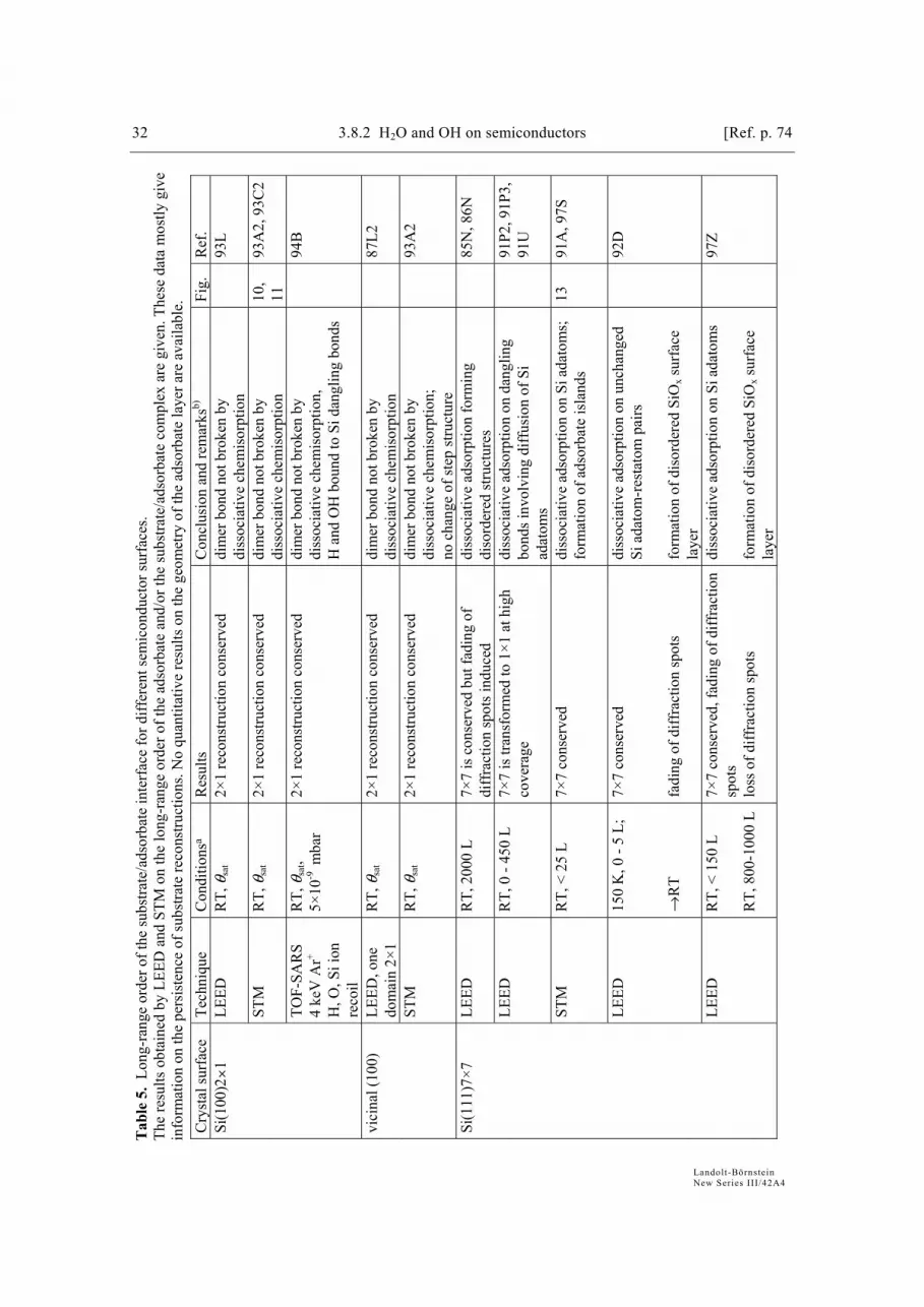
32 3.8.2 H2O and OH on semiconductors [Ref. p. 74
Landolt-Börnstein New Series III/42A4
Tab
le 5
. Lo
ng-r
ange
ord
er o
f the
subs
trate
/ads
orba
te in
terf
ace
for d
iffer
ent s
emic
ondu
ctor
surf
aces
. Th
e re
sults
obt
aine
d by
LEE
D a
nd S
TM o
n th
e lo
ng-r
ange
ord
er o
f the
ads
orba
te a
nd/o
r the
subs
trate
/ads
orba
te c
ompl
ex a
re g
iven
. The
se d
ata
mos
tly g
ive
info
rmat
ion
on th
e pe
rsis
tenc
e of
subs
trate
reco
nstru
ctio
ns. N
o qu
antit
ativ
e re
sults
on
the
geom
etry
of t
he a
dsor
bate
laye
r are
ava
ilabl
e.
Cry
stal
surf
ace
Tech
niqu
e C
ondi
tions
a R
esul
ts
Con
clus
ion
and
rem
arks
b)
Fig.
R
ef.
LEED
RT,
θsa
t 2×
1 re
cons
truct
ion
cons
erve
d
dim
er b
ond
not b
roke
n by
di
ssoc
iativ
e ch
emis
orpt
ion
93
L
STM
RT,
θsa
t 2×
1 re
cons
truct
ion
cons
erve
d
dim
er b
ond
not b
roke
n by
di
ssoc
iativ
e ch
emis
orpt
ion
10,
11
93A
2, 9
3C2
Si(1
00)2×
1
TOF-
SAR
S 4
keV
Ar+
H, O
, Si i
on
reco
il
RT,
θsa
t,
5×10
-9 m
bar
2×
1 re
cons
truct
ion
cons
erve
d di
mer
bon
d no
t bro
ken
by
diss
ocia
tive
chem
isor
ptio
n,
H a
nd O
H b
ound
to S
i dan
glin
g bo
nds
94
B
LE
ED, o
ne
dom
ain
2×1
RT,
θsa
t
2×1
reco
nstru
ctio
n co
nser
ved
dim
er b
ond
not b
roke
n by
di
ssoc
iativ
e ch
emis
orpt
ion
87
L2
vi
cina
l (10
0)
STM
RT,
θsa
t
2×1
reco
nstru
ctio
n co
nser
ved
dim
er b
ond
not b
roke
n by
di
ssoc
iativ
e ch
emis
orpt
ion;
no
cha
nge
of st
ep st
ruct
ure
93
A2
LE
ED
RT,
200
0 L
7×7
is c
onse
rved
but
fadi
ng o
f di
ffra
ctio
n sp
ots i
nduc
ed
diss
ocia
tive
adso
rptio
n fo
rmin
g di
sord
ered
stru
ctur
es
85
N, 8
6N
LE
ED
RT,
0 -
450
L 7×
7 is
tran
sfor
med
to 1
×1 a
t hig
h co
vera
ge
diss
ocia
tive
adso
rptio
n on
dan
glin
g bo
nds i
nvol
ving
diff
usio
n of
Si
adat
oms
91
P2, 9
1P3,
91
U
ST
M
RT,
< 2
5 L
7×
7 co
nser
ved
diss
ocia
tive
adso
rptio
n on
Si a
dato
ms;
fo
rmat
ion
of a
dsor
bate
isla
nds
13
91A
, 97S
LEED
15
0 K
, 0 -
5 L;
→
RT
7×7
cons
erve
d fa
ding
of d
iffra
ctio
n sp
ots
diss
ocia
tive
adso
rptio
n on
unc
hang
ed
Si a
dato
m-r
esta
tom
pai
rs
form
atio
n of
dis
orde
red
SiO
x sur
face
la
yer
92
D
Si(1
11)7
×7
LEED
R
T, <
150
L
RT,
800
-100
0 L
7×7
cons
erve
d, fa
ding
of d
iffra
ctio
n sp
ots
loss
of d
iffra
ctio
n sp
ots
diss
ocia
tive
adso
rptio
n on
Si a
dato
ms
form
atio
n of
dis
orde
red
SiO
x sur
face
la
yer
97
Z
Ref. p. 74] 3.8.2 H2O and OH on semiconductors 33
Landolt-Börnstein New Series III/42A4
Cry
stal
surf
ace
Tech
niqu
e C
ondi
tions
a R
esul
ts
Con
clus
ion
and
rem
arks
b)
Fig.
R
ef.
Si(1
11)2
×1
LEED
LT
, 2L
→ R
T
2×1
lost
1×
1 re
cons
truct
ion
form
ed
π-bo
nded
cha
ins b
roke
n by
dis
soci
ativ
e ad
sorp
tion
85
S
Si(1
13)(
3×2)
LE
ED
RT,
10
% o
f θsa
t tra
nsfo
rmat
ion
3×2
→ 3
×1
trans
form
atio
n of
reco
nstru
ctio
n in
duce
d by
diss
ocia
tive a
dsor
ptio
n
93J
G
e(10
0)
c(4×
2)/2
×1
LEED
16
0 K
, 0 -
5 L
→
RT
c(4×
2) →
2×1
wea
k 2×
1 w
eak
→ 2
×1 sh
arp
mol
ecul
ar a
dsor
ptio
n at
LT
diss
ocia
tive
adso
rptio
n on
Ge
dim
ers
89
L, 9
1L1,
91
L2
G
e(10
0)2×
1 LE
ED
100
K, 1
L
2×
1 is
con
serv
ed
mol
ecul
ar a
nd d
isso
ciat
ive
adso
rptio
n on
Ge
dim
ers
91
P1
G
e(11
1)2×
1
LEED
R
T, <
10
L >
10 L
2×1→
1×1
or 8
×2
loss
of d
iffra
ctio
n sp
ots
diss
ocia
tive
adso
rptio
n on
2
adso
rptio
n sit
es;
area
of 5
0-30
0 su
rfac
e at
oms
invo
lved
/per
ads
orbe
d w
ater
mol
ecul
e.
form
atio
n of
dis
orde
red
surf
ace
oxid
e la
yer
7 73
H, 7
5S,
79G
GaA
s(10
0)1×
1 LE
ED
RT,
< 4
×103
L 1×
1 re
cons
truct
ion
cons
erve
d
81
T G
aAs(
110)
1×1
LEED
R
T, <
105
L,
θ ≤
1 M
L 1×
1 re
cons
truct
ion
cons
erve
d I(
V) c
urve
s ind
icat
e lo
ss o
f rel
axat
ion
84
M
10
0K, <
0.5
L →
RT
1×1
reco
nstru
ctio
n co
nser
ved,
fa
ding
of d
iffra
ctio
n sp
ots
diss
ocia
tive
adso
rptio
n on
Ga-
As
surf
ace
pairs
on
set o
f sur
face
oxi
datio
n
97
H
InP(
100)
1×1
LEED
R
T, 1
04 -105
L R
T, >
109 L
parti
al lo
ss o
f 1×1
spot
s lo
ss o
f diff
ract
ion
spot
s
mol
ecul
ar a
dsor
ptio
n ox
ide
form
atio
n
82
M
In
P(11
0)1×
1 LE
ED
100
K, <
0.5
L
→ R
T
1×1
reco
nstru
ctio
n co
nser
ved
fadi
ng o
f diff
ract
ion
spot
s
diss
ocia
tive
adso
rptio
n on
In-P
surf
ace
pairs
on
set o
f sur
face
oxi
datio
n
00
H
a Exp
erim
enta
l con
ditio
ns a
s giv
en in
the
refe
renc
es

34 3.8.2 H2O and OH on semiconductors [Ref. p. 74
Landolt-Börnstein New Series III/42A4
Tab
le 6
. Val
ence
ban
d el
ectro
n st
ates
, bin
ding
ene
rgie
s, an
d as
sign
men
ts fo
r diff
eren
t sem
icon
duct
or su
rfac
es a
nd a
dsor
ptio
n co
nditi
ons.
Onl
y fo
r phy
siso
rbed
H2O
the
mea
sure
d el
ectro
n st
ates
are
stri
ctly
ads
orba
te m
olec
ular
orb
ital s
tate
s. Fo
r che
mis
orbe
d sp
ecie
s th
e m
easu
red
elec
tron
state
s re
sult
from
ads
orba
te s
tate
s w
hich
stro
ngly
hyb
ridiz
e w
ith s
ubst
rate
sta
tes
(sem
icon
duct
or d
angl
ing
bond
s) i
n co
vale
nt b
ond
form
atio
n. T
he s
tate
s as
m
easu
red
on d
iffer
ent
sem
icon
duct
or s
urfa
ces
and
for
diff
eren
t ad
sorp
tion
cond
ition
s ar
e gi
ven
toge
ther
with
the
ir as
sign
men
ts.
Als
o re
sults
fro
m
theo
retic
al c
alcu
latio
ns fo
r diff
eren
t ads
orpt
ion
geom
etrie
s are
pre
sent
ed h
ere.
C
ryst
al
surf
ace
Tech
niqu
e
Con
ditio
nsa
Ref
e-re
nce
leve
lb
Bin
ding
en
ergi
es
[eV
]
Mol
ecul
ar
orbi
tal
assi
gnm
entc a
s gi
ven
in R
ef.
Add
ition
al in
form
atio
n or
as
sign
men
t by
auth
ors
of d
ata
colle
ctio
n
Rem
arks
d Fi
g R
ef
UPS
, HeI
30
0 K
, 1 L
- 10
0 L
E F
6.1
8.0
10.6
1b1 o
f H2O
3a
1 of H
2O
1b2 o
f H2O
assi
gnm
ent q
uest
iona
ble
(spe
ctra
unc
lear
, pr
obab
ly d
ue to
be
ginn
ing
oxid
atio
n?)
81
F1
SX
PS,
hν=5
1eV
30
0K, θ
sat
E VBM
6
.2
7.2
11
.5
1b1 o
f H2O
3a
1 of H
2O
1b2 o
f H2O
OH
-1π
O
H-1
π
OH
-3σ
mol
ecul
ar a
dsor
ptio
n as
sum
ed
(spe
ctra
due
to
diss
ocia
tion
?)
15
83S2
UPS
, HeI
I 16
0 K
, 1.5
L
anne
aled
300
K
E vac
10
.9
11.7
16
.2
O lo
ne p
air
Si
O-H
Si-O
H
84
O
300
K,
0.7-
1000
L
E F
6.6
7.6
11.9
assi
gnm
ents
le
ft op
en
OH
-1π
O
H-1
π
OH
-3σ
cylin
dric
al S
i cry
stal
; di
ffer
ence
spec
tra
1000
L -
0.7
L ar
e si
mila
r to
the
spec
tra
pres
ente
d by
[81F
1]
85
R1
10
0 K
, <
0.3
L E F
6.
6 7.
6 11
.9
assi
gnm
ents
left
open
OH
-1π
O
H-1
π
OH
-3σ
spec
tra id
entic
al to
RT
spec
tra
16
100
K,
0.3
- 0.7
L
E F
6.8
9.2
12.9
mol
ecul
ar H
2O
1b1
3a1
1b2
phys
isor
bed
H2O
16
Si(1
00)2
×1
UPS
, HeI
100
K,
> 0.
7 L
E F
7.2
10.2
13
.3
mol
ecul
ar H
2O
1b1
3a1
1b2
cond
ense
d ic
e la
yer
16
85R
1

Ref. p. 74] 3.8.2 H2O and OH on semiconductors 35
Landolt-Börnstein New Series III/42A4
Cry
stal
su
rfac
e Te
chni
que
C
ondi
tions
a R
efe-
renc
e le
velb
Bin
ding
en
ergi
es
[eV
]
Mol
ecul
ar
orbi
tal
assi
gnm
entc a
s gi
ven
in R
ef.
Add
ition
al in
form
atio
n or
as
sign
men
t by
auth
ors
of d
ata
colle
ctio
n
Rem
arks
d Fi
g R
ef
UPS
, HeI
SX
PS,
h ν=7
3eV
300
K,
0.06
ML
- θsa
t; 23
3 K
, θsa
t
E VBM
6.2
7
.2
11.5
24
.5
O-2
p of
OH
O
-2p
of O
H
O-2
p of
OH
O
-2s o
f OH
OH
-1π
O
H-1
π
OH
-3σ
O
-2s o
f OH
OH
adso
rbed
on
dim
er
dang
ling
bond
s; E V
BM is
ta
ken
at th
e Fer
mi e
dge
of th
e sur
face
stat
e of
clea
n Si
(100
)2×1
85
R3,
90
S,
96R
2
SXPS
, h ν
=30
eV
300
K, 1
0 L
- θsa
t E V
BM
6.3
11.2
Si
-OH
Si
O-H
OH
ads
orbe
d on
dim
er
dang
ling
bond
s;
87
L1
A
RU
PS,
h ν=5
0 eV
p-
pola
rized
RT,
θsa
t E V
BM
6.1
7
.1
11.4
OH
-1π
OH
-σ
vici
nal (
100)
on
e do
mai
n (2
×1);
no d
ispe
rsio
n ob
serv
ed o
n ch
angi
ng
the
emis
sion
ang
le
88
M
SX
PS,
hν=3
6 eV
R
T, θ
sat
E F
6.5
7.5
11.9
O-2
p Si
O-H
Si
-OH
O
H a
dsor
bed
on d
imer
da
nglin
g bo
nds;
vi
cina
l (10
0)
one
dom
ain
(2×1
)
89
F
SXPS
, hν
=30e
V
300
K, θ
sat
E VBM
6
.3
7.4
11
.2
OH
-1π
OH
-1π
OH
-3σ
Oπ
nonb
ondi
ng
Si-O
H w
eak
bond
ing
OH
ads
orbe
d on
dim
er
dang
ling
bond
s
91L1
UPS
, HeI
I
295
K, θ
sat
E F
5
6.4
7
.6
11.9
Si-H
O
H
SiO
-H
Si-O
H
Si-s
p3 +
H-1
s
O-2
p lo
ne p
air
O-2
p +
H-1
s Si
-sp3
+ O
-2p
OH
ads
orbe
d on
dim
er
dang
ling
bond
s
94S1
THEO
RY
ex
tend
ed
Hüc
kel
E v
ac
12.1
14
.8
18.5
OH
-1π
OH
-3σ
Si-O
H
O-π
non
bond
ing
O-p
+ H
-s
Si-s
+ O
-p, σ
bon
ding
OH
ads
orbe
d on
dim
er
dang
ling
bond
s
83
C1,
83
C2
Si(1
00)2
×1
THEO
RY
tig
ht b
indi
ng
appr
oach
E v
ac
12.2
16
.0
18.8
OH
O
H-3
σ Si
-OH
O-p
, O-π
non
bond
ing
O-p
+ H
-s
Si-s
+ O
-p, σ
bon
ding
OH
ads
orbe
d on
dim
er
dang
ling
bond
s;
87
K1

36 3.8.2 H2O and OH on semiconductors [Ref. p. 74
Landolt-Börnstein New Series III/42A4
Cry
stal
su
rfac
e Te
chni
que
C
ondi
tions
a R
efe-
renc
e le
velb
Bin
ding
en
ergi
es
[eV
]
Mol
ecul
ar
orbi
tal
assi
gnm
entc a
s gi
ven
in R
ef.
Add
ition
al in
form
atio
n or
as
sign
men
t by
auth
ors
of d
ata
colle
ctio
n
Rem
arks
d Fi
g R
ef
THEO
RY
tig
ht b
indi
ng
appr
oach
E v
ac
12.2
18
.4
20.0
35
.8
1b1 o
f H2O
1b
2 of H
2O
σ o
f Si-O
H2
2a1
of H
2O
O-p
+ S
i-s, σ
bon
ding
mol
ecul
ar H
2O
adso
rptio
n; v
alue
s gi
ven
for 1
80°
orie
ntat
ion;
als
o di
ffer
ent o
rient
atio
ns
of th
e bo
nd d
irect
ion
ca
lcul
ated
87
K1
Si(1
00)2
×1
THEO
RY
fu
lly se
lf-co
nsis
tent
ca
lcul
atio
n
E v
ac
14.3
8 15
.58
19.9
9
OH
O
H
Si-O
H
O-p
Si
-s +
O-p
OH
ads
orbe
d on
dim
er
dang
ling
bond
s
89F
300
K,
2 - 1
70 L
E F
6.
6 7.
6 11
.9
assi
gnm
ents
le
ft op
en
OH
-1π
O
H-1
π
OH
-3σ
for l
ow e
xpos
ures
sa
me
spec
tral f
eatu
res
as o
n Si
(100
) RT,
θsa
t
17
100K
, 0.
45L
E F
6.8
9.2
12.9
mol
ecul
ar H
2O
1b1
3a
1
1b2
phys
isor
bed
H2O
16
Si(1
10)
UPS
, HeI
100K
, >
0.45
L E F
7.
2 10
.2
13.3
mol
ecul
ar H
2O
1b1
3a
1
1b2
cond
ense
d ic
e la
yer
85R
1
EELS
R
T, 1
0 - 1
00 L
; 15
0 K
, 0.2
5 - 5
L
3
.7
4.7
8
.7
no a
ssig
nmen
t gi
ven
trans
ition
s fro
m o
ccup
ied
to u
nocc
upie
d st
ates
extri
nsic
surf
ace
stat
es
indu
ced
by H
2O,
mol
ecul
ar a
dsor
ptio
n as
sum
ed
9b
75F,
77
F,
92D
Si(1
11)7
×7
UPS
, HeI
R
T, <
135
L; 1
00
K, 2
.5 L
→R
T E F
6.
5 7.
5 1
1
H2O
-orb
itals
O
H-1
π
OH
-1π
Si
-3σ
mol
ecul
ar a
dsor
ptio
n as
sum
ed
(spe
ctra
due
to
diss
ocia
tion
?)
17
85R
1,
85R
2,
86S2

Ref. p. 74] 3.8.2 H2O and OH on semiconductors 37
Landolt-Börnstein New Series III/42A4
Cry
stal
su
rfac
e Te
chni
que
C
ondi
tions
a R
efe-
renc
e le
velb
Bin
ding
en
ergi
es
[eV
]
Mol
ecul
ar
orbi
tal
assi
gnm
entc a
s gi
ven
in R
ef.
Add
ition
al in
form
atio
n or
as
sign
men
t by
auth
ors
of d
ata
colle
ctio
n
Rem
arks
d Fi
g R
ef
UPS
, HeI
R
T, <
103 L
E F
~
6 ~
8 ~
11
1b1 o
f H
2O
3a1
of
H2O
1b
2 of
H2O
assi
gnm
ent q
uest
iona
ble
mol
ecul
ar a
dsor
ptio
n as
sum
ed
(spe
ctra
due
to o
nset
of
oxi
datio
n?)
17
79F,
81
F1,
81F2
, 85
R1,
85
R2
UPS
SX
PS,
h ν =
36
eV
RT
E F
6.2
7.
2 11
.6
OH
Si
O-H
Si
-OH
O-2
p lo
ne p
air
O-2
p +H
-1s
Si-s
p3 +O-2
p
diss
ocia
tive
adso
rptio
n of
H2O
; em
issi
on
dom
inat
ed b
y Si
-OH
gr
oups
89
F
Si(1
11)7
×7
UPS
, HeI
< 10
0 K
E F
~
7 ~
9-10
~
13
1b1 o
f H
2O
3a1
of
H2O
1b
2 of
H2O
fo
r low
exp
osur
es
phys
isor
bed
H2O
, the
n co
nden
sed
ice
laye
r; sp
ectra
as o
n Si
(110
), se
e Fi
g. 2
3
85
R1,
85
R2,
85
R3,
86
S2
TH
EOR
Y
Ext.
Hüc
kel
mol
ecul
ar
E vac
12
.0
18.8
19
.4
36.6
1b1 o
f H2O
3a
1 of S
i-OH
2 1b
2 of
H2O
2a
1 of H
2O
O-p
x, no
nbon
ding
O
-pz +
Si-s
, bon
ding
H2O
on
top
of S
i da
nglin
g bo
nd
83
C1
TH
EOR
Y
Ext.
Hüc
kel
diss
ocia
tive
E v
ac
9.9
12
.1
14.8
18
.5
33.8
Si-H
O
H-1
π x
OH
-3σ
Si-O
H
OH
-2σ
H-1
s + S
i-sp,
σ b
ondi
ng
O-p
x, O
-π n
onbo
ndin
g O
-pz +
Si-s
, σ b
ondi
ng
Si-O
H a
nd S
i-H o
n to
p of
Si d
angl
ing
bond
83
C2
m
olec
ular
E v
ac
12.2
18
.4
19.2
35
.8
1b1 o
f H
2O
1b2 o
f H
2O
3a1 of
Si-O
H2
2a1 o
f H
2O
H
2O o
n to
p of
Si
dang
ling
bond
pe
rpen
dicu
lar t
o su
rfac
e
87
K1
Si(1
11)
THEO
RY
tig
ht b
indi
ng
mol
ecul
ar
E vac
14
.6
19.2
35.8
3a1 o
f H
2O
1b2 o
f H
2O
2a1 o
f H
2O
and
O-p
y+Si
-s, O
-σ
bond
ing
H2O
on
top
of S
i da
nglin
g bo
nd ,
para
llel t
o su
rfac
e
87
K1

38 3.8.2 H2O and OH on semiconductors [Ref. p. 74
Landolt-Börnstein New Series III/42A4
Cry
stal
su
rfac
e Te
chni
que
C
ondi
tions
a R
efe-
renc
e le
velb
Bin
ding
en
ergi
es
[eV
]
Mol
ecul
ar
orbi
tal
assi
gnm
entc a
s gi
ven
in R
ef.
Add
ition
al in
form
atio
n or
as
sign
men
t by
auth
ors
of d
ata
colle
ctio
n
Rem
arks
d Fi
g R
ef
Si(1
11)
THEO
RY
tig
ht b
indi
ng
diss
ocia
tive
E v
ac
10
12.2
16
18.8
33
.2
Si-H
O
H-1
π O
H-3
σ
Si-O
H
OH
-2σ
Si-p
z + H
-1s,
σ-bo
ndin
g O
-px l
one
pair,
π
non
bond
ing
O-p
z + S
i-s, O
-σ b
ond.
Si-O
H a
nd S
i-H o
n to
p of
Si d
angl
ing
bond
87
K1
Si
(113
), Si
(115
), Si
(5,5
,12)
, Si
(112
)
UPS
, HeI
I R
T, θ
sat
E F
6.2
7.2
11.5
emis
sion
shap
e
ch
arac
teris
tic
for O
H +
H
OH
-1π
O
H-1
π
Si-3
σ
diss
ocia
tive
adso
rptio
n of
H2O
; orie
ntat
ion
depe
nden
t sat
urat
ion
cove
rage
s der
ived
and
re
late
d to
the
num
ber
of d
imer
s and
ada
tom
-lik
e re
bond
ed a
tom
s at
step
s
18
97R
110
K, 0
.4 L
E V
BM
5.9
9.8
12
.9
1b1 o
f H
2O
3a1
of
H2O
1b
2 of
H2O
H
2O m
onom
ers
110K
, 1.1
L
E V
BM
6.1
8.5
10
.0
12.9
1b1 o
f H
2O
3a1
of
H2O
3a
1 o
f H
2O
1b2 o
f H
2O
H
2O d
imer
s with
H-
bond
ing;
3a
1 M
O is
split
by
dim
er b
ond
110K
, 3.7
L
E VBM
6.
3
8.8
9.
9 12
.9
1b1 o
f H
2O
3a1
of
H2O
3a
1 o
f H
2O
1b2 o
f H
2O
H
2O ic
e cl
uste
r; 3a
1 M
O is
bro
aden
ed
19
Ge(
100)
2×1
UPS
, HeI
110
K, 3
.7 L
→
300
K
E VBM
5
.6
7.5
9
.2
10
.0
OH
-π
OH
-π
OH
-σp
nonb
ondi
ng
Ge-
OH
bon
ding
as
sign
men
t unc
lear
ther
mal
ly in
duce
d di
ssoc
iatio
n
20
87K
3

Ref. p. 74] 3.8.2 H2O and OH on semiconductors 39
Landolt-Börnstein New Series III/42A4
Cry
stal
su
rfac
e Te
chni
que
C
ondi
tions
a R
efe-
renc
e le
velb
Bin
ding
en
ergi
es
[eV
]
Mol
ecul
ar
orbi
tal
assi
gnm
entc a
s gi
ven
in R
ef.
Add
ition
al in
form
atio
n or
as
sign
men
t by
auth
ors
of d
ata
colle
ctio
n
Rem
arks
d Fi
g R
ef
160
K,
0.5
- 100
L
→ 3
00 K
E VBM
5.5
7.3
9
.3
10.4
OH
-π
OH
-π
Ge-
H
OH
-σp
nonb
ondi
ng
liftin
g of
deg
ener
acy
ther
mal
ly in
duce
d di
ssoc
iatio
n
SXPS
, hν
= 6
0 eV
160
K,
0.5
- 100
L
E VBM
5
.9-6
.5
8.1
-8.4
12
.4-1
2.7
1b1 o
f H
2O
3a1
of
H2O
1b
2 of
H2O
H
2O ic
e la
yer
89L,
91
L1
SXPS
, hν
=17,
20,2
4 eV
160
K,
2 L
→30
0 K
E F
~
4.8
~ 5.
8 ~
7.8
~ 9.
5 ~1
0.6
Ge-
H
OH
-π
Ge-
OH
-π
Ge-
H
OH
-σ
nonb
ondi
ng
wea
k bo
ndin
g
disp
ersi
on
inve
stig
ated
, onl
y w
eak
disp
ersi
on
obse
rved
21,
22
91L2
E vac
12
16
.9
Ge-
OH
-π
Ge-
OH
-σp
O
H o
n to
p si
te
diss
ocia
tive
E vac
12
16
.8
15.8
Ge-
OH
-πa
Ge-
OH
-πb
Ge-
OH
-σ
O
H o
n br
idge
site
be
twee
n tw
o G
e
Ge(
100)
2×1
THEO
RY
LC
AO
xα
mol
ecul
ar
E vac
12
.2
14.5
19
1b1
of H
2O
3a1
of H
2O
1b2
of H
2O
H
2O o
n to
p si
te
91S
110
K, 0
.3 -
3 L
E VBM
6.
4-6.
6 8.
9
9.9
13.0
1b1 o
f H
2O
3a1
of
H2O
3a
1 o
f H
2O
1b2 o
f H
2O
H
2O ic
e cl
uste
r, 3a
1 spl
ittin
g du
e to
H
-bon
ding
23
Ge(
111)
2×8
UPS
110
K, 3
L
→30
0 K
E V
BM
5.2
7.6
10.2
OH
-π
OH
-π
Ge-
OH
-σp
nonb
ondi
ng
Ge-
OH
bon
ding
th
erm
ally
indu
ced
diss
ocia
tion;
ad
ditio
nal e
mis
sion
s (d
ue to
coa
dsor
bed
mol
ecul
ar H
2O?)
20
87K
3

40 3.8.2 H2O and OH on semiconductors [Ref. p. 74
Landolt-Börnstein New Series III/42A4
Cry
stal
su
rfac
e Te
chni
que
C
ondi
tions
a R
efe-
renc
e le
velb
Bin
ding
en
ergi
es
[eV
]
Mol
ecul
ar
orbi
tal
assi
gnm
entc a
s gi
ven
in R
ef.
Add
ition
al in
form
atio
n or
as
sign
men
t by
auth
ors
of d
ata
colle
ctio
n
Rem
arks
d Fi
g R
ef
180
K
E VBM
3.
2
5
9.4
H2O
orb
itals
1b
1
3a1
1b
2
phys
isor
bed
H2O
as
sum
ed (o
rigin
of
spec
tral f
eatu
res
uncl
ear ?
)
U
PS, H
eI
300
K,
104 L
E VBM
3.
2 4.
4 8.
4
H2O
orb
itals
1b1
3a
1
1b2
chem
isor
bed
H2O
as
sum
ed (o
rigin
of
spec
tral f
eatu
res
uncl
ear ?
)
79B
~100
K, 0
.5 L
E V
BM
5 7 9.1
12.1
Ga-
OH
A
s-H
G
a-O
H
As-
H
di
ssoc
iativ
ely
adso
rbed
H2O
(g
iven
ass
ignm
ent
uncl
ear?
)
24
96H
, 97
H
GaA
s (11
0)
SXPS
, hν
= 4
1eV
~100
K, >
2L
E VBM
5
.5
8
12
1b1 of
H2O
3a
1 of
H2O
1b
2 of
H2O
ph
ysis
orbe
d H
2O, i
ce
laye
r 24
GaA
s (1
00)
UPS
R
T,
7×10
12 L
6
.1
10.9
O
H o
rbita
ls
diss
ocia
tivel
y ad
sorb
ed H
2O
(orig
in o
f em
issi
ons
uncl
ear?
)
82
W
10
0 K
, 0.5
L
E VBM
4.
2 6 8.
4
11.1
In-O
H
P-H
In
-OH
P-
H
di
ssoc
iativ
ely
adso
rbed
H2O
(g
iven
ass
ignm
ent
uncl
ear?
)
25
InP(
110)
SX
PS,
hν =
41
eV
100
K, >
1.3
L
E VBM
5.
7 8.
1 11
.6
1b1 of
H2O
3a
1 of
H2O
1b
2 of
H2O
ph
ysis
orbe
d H
2O, i
ce
laye
r
00H
FeS 2
(100
) U
PS, H
eI
100
K, 0
.5 -
1.5
L E F
~7
~1
0 ~1
3
1b1 of
H2O
3a
1 of
H2O
1b
2 of
H2O
m
olec
ular
ads
orpt
ion
pr
efer
entia
lly o
n Fe
-si
tes
91
P2
G
aSe(
0001
) SX
PS,
h ν =
21
eV
100
K,
0.5
L - 7
L
6
.5-7
.3
9.5
-10
12.7
-13.
2
1b1 of
H2O
3a
1 of
H2O
1b
2 of
H2O
co
nden
sed
ice
laye
r; E B
F dep
endi
ng o
n co
vera
ge;
92
M,
93M

Ref. p. 74] 3.8.2 H2O and OH on semiconductors 41
Landolt-Börnstein New Series III/42A4
Cry
stal
su
rfac
e Te
chni
que
C
ondi
tions
a R
efe-
renc
e le
velb
Bin
ding
en
ergi
es
[eV
]
Mol
ecul
ar
orbi
tal
assi
gnm
entc a
s gi
ven
in R
ef.
Add
ition
al in
form
atio
n or
as
sign
men
t by
auth
ors
of d
ata
colle
ctio
n
Rem
arks
d Fi
g R
ef
E F
6.8-
7.7
9.5-
10.3
13
.0-1
3.9
1b1 of
H2O
3a
1 of
H2O
1b
2 of
H2O
In
Se(0
001)
SX
PS
hν =
21
eV
h ν =
30
eV
100
K,
0.1
L - 1
0 L
E vac
11
.4
14
17.6
1b1 of
H2O
3a
1 of
H2O
1b
2 of
H2O
cond
ense
d ic
e la
yer;
E BF st
rong
ly d
epen
-di
ng o
n co
vera
ge a
nd
subs
trate
dop
ing;
io
nisa
tion
ener
gies
E B
vac w
eakl
y de
pen-
ding
on
cove
rage
26
92M
, 93
M
M
oSe 2
(0
001)
U
PS
80 K
, 0.5
- 5
ML
E vac
~1
1.2
~13.
5 ~1
7
1b1 of
H2O
3a
1 of
H2O
1b
2 of
H2O
co
nden
sed
H2O
; io
nisa
tion
ener
gies
E B
vac n
early
con
stan
t;
dipo
le b
etw
een
subs
trate
and
ad
sorb
ate
assu
med
75
Y
M
oS2
(000
1)
UPS
10
0 K
E F
~7
~1
0 ~1
3
1b1 of
H2O
3a
1 of
H2O
1b
2 of
H2O
co
nden
sed
ice
laye
r
87
J, 88
J
E F
6.4-
8.0
9.2-
10.9
12
.3-1
4.3
25.9
-27.
9
1b1 of
H2O
3a
1 of
H2O
1b
2 of
H2O
2a
1 of
H2O
W
Se2
(000
1)
UPS
SX
PS
h ν =
21
eV
hν =
30
eV
100
K, 1
- 10
.5 L
Evac
11.0
-11.
4 ~
14
16.9
-17.
5 30
.4-3
1.3
1b1 of
H2O
3a
1 of
H2O
1b
2 of
H2O
2a
1 of
H2O
cond
ense
d ic
e la
yer;
E BF d
epen
ding
on
cove
rage
and
subs
trate
do
ping
; ion
isat
ion
ener
gies
EBva
c nea
rly
inde
pend
ent o
n co
vera
ge; d
ipol
e be
twee
n su
bstra
te a
nd
adso
rbat
e as
sum
ed
92
M,
93M
, 96
M
CuI
nSe 2
(0
01)
UPS
80 K
, 0.0
1 - 1
0 L
E F
~7.3
~9
.9
~13
1b1 of
H2O
3a
1 of
H2O
1b
2 of
H2O
m
olec
ular
ly a
dsor
bed
H2O
92S
a E
xper
imen
tal c
ondi
tions
as g
iven
in th
e re
fere
nces
b E
F: F
erm
i lev
el;
E vac
: vac
uum
leve
l; E V
BM: v
alen
ce b
and
max
imum
c F
or a
det
aile
d pr
esen
tatio
n of
the
orbi
tal a
ssig
nmen
t see
text
of s
ectio
n 3.
8.2.
11; S
i-OH
indi
cate
s Si-O
H b
ondi
ng st
ate,
SiO
-H in
dica
tes O
-H b
ondi
ng st
ate.
d R
emar
ks in
par
enth
esis
like
e.g
. (sp
ectra
due
to d
isso
ciat
ion
?) a
re g
iven
by
the
auth
ors o
f thi
s dat
a co
llect
ion

42 3.8.2 H2O and OH on semiconductors [Ref. p. 74
Landolt-Börnstein New Series III/42A4
Tab
le 7
. C
ore
leve
l ele
ctro
n bi
ndin
g en
ergi
es E
B of
H2O
ads
orba
te s
peci
es a
nd b
indi
ng e
nerg
y sh
ifts
∆EB
of s
ubst
rate
em
issi
ons
obta
ined
for
diff
eren
t se
mic
ondu
ctor
surf
aces
and
ads
orpt
ion
cond
ition
s. C
ore
leve
l bin
ding
ene
rgy
shift
s mea
sure
d fo
r the
subs
trate
line
s as w
ell a
s the
bin
ding
ene
rgie
s of t
he a
dsor
bate
line
s are
pre
sent
ed h
ere,
as t
hey
have
bee
n us
ed fo
r the
det
erm
inat
ion
of a
dsor
ptio
n m
ode
and
adso
rbat
e pr
oper
ties.
Cry
stal
/ su
rfac
e Te
chni
que
hν [e
V]
Con
ditio
nsa
Cor
e le
vel
E B
[eV
] ∆E
B [e
V]
Ass
ignm
entb,
c
Rem
arks
c Fi
g.
Ref
.
SXPS
h ν
= 1
20
300
K, θ
sat
Si 2
p 3/2
+0.9
Si
-OH
2 (S
i-OH
?)
mol
ecul
ar a
dsor
ptio
n as
sum
ed
(shi
ft du
e to
Si-O
H?)
83S2
350
K, 2
L, θ
sat
Si 2
p 3/2
98
.74
–0
.46
+0.8
0
bulk
O
DA
(cle
an)
Si-O
H
OD
A d
isap
pear
ed a
fter s
atur
atio
n; S
i-OH
in
tens
ity e
qual
to o
rigin
al O
DA
inte
nsity
→ 6
40 K
Si
2p 3
/2
+1
.0
+1.8
Si
+
Si2+
af
ter a
nnea
ling
to 6
40 K
Si+ an
d Si
2+
oxid
atio
n st
ates
form
ed
SXPS
h ν
=13
8.5
→ 8
70 K
Si
2p 3
/2
+2
.6
+3.5
Si
3+
Si4+
af
ter a
nnea
ling
to 8
70 K
adi
tiona
l Si3+
an
d Si
4+ e
mis
sion
s and
OD
A in
tens
ity
rest
ored
85R
3
Si(1
00)2
×1
SXPS
h ν
= 1
30
300
K, 1
0L, θ
sat
Si 2
p 3/2
–0.4
3 +0
.25
+1
.00
OD
A(c
lean
) Si
-H
Si-O
H
OD
A in
tens
ity st
rong
ly d
ecre
ased
afte
r sa
tura
tion;
no
oxi
datio
n ob
serv
ed
87
L1
R
T, 2
L, θ
sat,
(100
) vic
inal
, on
e do
mai
n 2×
1 LE
ED
Si 2
p 3/2
–0.5
2 +0
.31
+1.0
0
OD
A(c
lean
) Si
-H
Si-O
H
OD
A in
tens
ity st
rong
ly d
ecre
ased
afte
r sa
tura
tion;
no
oxi
datio
n ob
serv
ed
27
88M
SXPS
h ν
= 1
30
300
K, 5
L, θ
sat
Si 2
p 3/2
–0.4
3 +0
.24
+1.0
4
OD
A(c
lean
) Si
-H
Si-O
H
OD
A in
tens
ity st
rong
ly d
ecre
ased
afte
r sa
tura
tion;
no
oxi
datio
n ob
serv
ed
91
L1
Si(1
00)
XPS
R
T, θ
sat;
→ 6
70 K
; →
920
K;
O 1
s re
ferr
ed to
Si
2p 3
/2
432.
8 43
2.2
433.
2
Si
-OH
Si
-O-S
i Si
-oxi
de su
b-st
oich
iom
etric
O1s
bin
ding
ene
rgy
mon
itore
d in
the
tem
pera
ture
rang
e 0
- 650
°C
94
S1

Ref. p. 74] 3.8.2 H2O and OH on semiconductors 43
Landolt-Börnstein New Series III/42A4
Cry
stal
/ su
rfac
e Te
chni
que
hν [e
V]
Con
ditio
nsa
Cor
e le
vel
E B
[eV
] ∆E
B [e
V]
Ass
ignm
entb,
c
Rem
arks
c Fi
g.
Ref
.
SXPS
h ν
= 1
45
90 K
, 1 -
80 L
Si
2p 3
/2
–0
.55
+0.3
0 +0
.85
+1.6
5 +2
.45
+3.3
5
OD
A(c
lean
) Si
-H
Si-O
H/S
i+
Si2+
Si
3+
Si4+
OD
A in
tens
ity sl
owly
dec
reas
ed w
ith
expo
sure
; Si
2+ a
lread
y ob
serv
ed a
t 5 L
; with
hig
her
expo
sure
s (80
L) a
lso
Si3+
and
Si4+
ob
serv
ed;
(sou
rce
indu
ced
enha
ncem
ent o
f oxi
datio
n?)
28
95P
Si(1
00)
SXPS
h ν
=145
30
0 K
, 1 -
40 L
Si
2p 3
/2
99.6
–0
.55
+0.8
5 +1
.65
bulk
O
DA
(cle
an)
Si-O
H/S
i+
Si2+
OD
A in
tens
ity sl
owly
dec
reas
ed w
ith
expo
sure
; (s
ourc
e in
duce
d en
hanc
emen
t of
oxid
atio
n?)
29
95P
X
PS
150
K,<
0.25
L;
150
K,
0.25
- 5
L;
→R
T
O1s
53
0.0
531.
7 53
0.2
Si-O
Si
-OH
Si
-O
prea
dsor
bed
stat
e (o
rigin
of s
pect
ral f
eatu
res u
ncle
ar?)
H
2O d
isso
ciat
ion
assu
med
su
rfac
e ox
ide
92D
Si(1
11)7
×7
SXPS
h ν
=145
30
0 K
, ≤ 9
0 L;
90
K, 4
0 L;
→
RT
Si 2
p 3/2
+0.8
9
Siad
-OH
O
H b
ondi
ng to
Si a
dato
m; s
low
at
tenu
atio
n of
rest
atom
inte
nsity
to 5
0%;
oxid
atio
n st
ates
up
to S
i4+at
RT
and
90 K
ob
serv
ed (s
ourc
e in
duce
d en
hanc
emen
t of
oxi
datio
n?)
30
95P
Si
(111
)2×1
X
PS
100
K,
0.2
- 2 L
; 10
0 K
, > 2
L;
RT,
θsa
t;
O1s
53
4.0
532.
6 53
4.6
532.
6
H
2O
Si-O
H
H2O
ice
Si-O
H
no c
hem
ical
ly sh
ifted
com
pone
nt in
Si 2
p lin
e ev
iden
t 31
85
S
Si(1
13)
SXPS
h ν
=13
5 R
T, 0
.01
- 2 L
Si
2p 3
/2
+0
.22
+0.9
0 Si
-H
Si-O
H
diss
ocia
tion
at d
imer
s ass
umed
96
S1

44 3.8.2 H2O and OH on semiconductors [Ref. p. 74
Landolt-Börnstein New Series III/42A4
Cry
stal
/ su
rfac
e Te
chni
que
hν [e
V]
Con
ditio
nsa
Cor
e le
vel
E B
[eV
] ∆E
B [e
V]
Ass
ignm
entb,
c
Rem
arks
c Fi
g.
Ref
.
SXPS
h ν
= 7
0 16
0 K
, 1 L
30
0 K
, 1 L
G
e 3d
5/2
–0
.43
+0.7
5 +0
.43
Ge
dim
er
(cle
an)
Ge-
OH
G
e-H
loss
of e
mis
sion
of G
e di
mer
due
to
adso
rbed
H2O
32
89
L,
91L1
Ge(
100)
2×1
SXPS
h ν
= 6
4 11
0 K
, 10
L →
360
K
Ge
3d5/
2
–0.4
5 +0
.56
0 ±0
.1
Ge
dim
er
(cle
an)
Ge-
OH
G
e-H
loss
of e
mis
sion
of G
e di
mer
due
to
adso
rbed
H2O
93R
1
100
K, 3
ML
O 1
s 53
3.2
H
2O
ice
laye
r
96S2
G
aAs(
100)
4×
6 X
PS
100
K, 3
ML
addt
iona
l
50 e
V e
lect
ron
beam
O 1
s 53
1.0-
531.
6 52
9.4-
530.
4
OH
G
a-ox
ide
elec
tron
indu
ced
diss
ocia
tion
of H
2O
96
S2
10
0 K
, < 0
.5 L
G
a 3d
5/2
As 3
d 5/2
+0.6
0 +0
.60
–0.6
5
Ga-
OH
A
s-H
A
s*
As*
due
to G
a-O
H fo
rmat
ion
G
aAs(
110)
SX
PS
hν =
60
h ν
= 8
0 R
T, 1
06 L
2×10
9 L-
4×10
10 L
Ga
3d5/
2 A
s 3d 5
/2
Ga
3d5/
2
+0
.6
+0.6
+1
.0
Ga-
OH
A
s-H
G
a-su
boxi
de
97H
GaA
s X
PS
RT,
7×1
012 L
Ga
3d
Ga
2p
O1s
530.
8
+1.6
+1
.7
Ga-
OH
G
a-O
H
Ga-
OH
diss
ocia
tive
adso
rptio
n as
sum
ed;
no b
indi
ng e
nerg
y sh
ift o
f As r
esol
ved;
(o
nset
of s
urfa
ce o
xida
tion?
)
82
W
G
aSe(
0001
) In
Se(0
001)
M
oS(0
001)
W
Se2(0
001)
SXPS
12
0 K
, 0.
5 - 3
.5 L
O
2s
26
.0
H2O
m
olec
ular
ads
orpt
ion,
no
chem
ical
ly
shift
ed su
bstra
te c
ompo
nent
s obs
erve
d;
adso
rbat
e bi
ndin
g en
ergy
shift
s ass
umed
to
be
due
to su
rfac
e di
pols
33
a,b
87J,
88J,
92M
, 93
M,
96M
a Ex
perim
enta
l con
ditio
ns a
s giv
en in
the
refe
renc
es
b Ass
ignm
ent a
s giv
en b
y th
e au
thor
s of t
he o
rigin
al p
aper
c R
emar
ks in
par
enth
esis
are
giv
en b
y th
e au
thor
s of t
his d
ata
colle
ctio
n
Ref. p. 74] 3.8.2 H2O and OH on semiconductors 45
Landolt-Börnstein New Series III/42A4
Tab
le 8
. Vib
ratio
nal p
rope
rties
of a
dsor
bed
H2O
or i
ts d
isso
ciat
ion
prod
ucts
for d
iffer
ent a
dsor
ptio
n co
nditi
ons o
n di
ffer
ent s
emic
ondu
ctor
surf
aces
V
ibra
tiona
l fre
quen
cies
of
adso
rbat
e/su
bstra
te b
ondi
ng: I
n th
is ta
ble
the
vibr
atio
nal m
odes
and
thei
r as
sign
men
ts o
btai
ned
afte
r ad
sorp
tion
on d
iffer
ent
sem
icon
duct
ors
and
for
vary
ing
adso
rptio
n co
nditi
ons
are
give
n. F
or c
hem
isor
bed
and
diss
ocia
tivel
y ad
sorb
ed s
peci
es t
he m
easu
red
eige
nmod
es a
nd
freq
uenc
ies d
epen
d on
the
spec
ific
surf
ace
mol
ecul
e fo
rmed
thus
bei
ng st
rong
ly in
fluen
ced
by su
bstra
te a
tom
s and
bon
ding
geo
met
ry.
Cry
stal
su
rfac
e A
dsor
bate
Tech
niqu
e
Con
ditio
nsa
V
ibra
tiona
l en
ergy
b [m
eV]
Vib
ratio
nal
freq
uenc
yb [c
m-1
]
Vib
ratio
nal m
ode
Con
clus
ion
and
rem
arks
Fi
g.
Ref
.
HR
EELS
E 0
= 1
4 eV
16
5 - 4
20 K
, 0.
1 - 1
L
78.1
10
1.7
259.
1 45
9.0
630
820
2090
37
00
Si-H
ben
d Si
-OH
stre
tch/
Si
-OH
ben
d Si
-H st
retc
h Si
O-H
stre
tch
diss
ocia
tive
adso
rptio
n;
Si-O
H st
retc
h al
so o
bser
ved
as
doub
le lo
ss a
t 160
0 cm
-1
34
82I2
IRA
S p
-pol
. 80
K, 1
0 L
20
7.1
~409
.0
16
70
~330
0 H
2O sc
isso
r H
2O st
retc
h co
nden
sed
mol
ecul
ar H
2O;
the
H2O
stre
tchi
ng m
ode
is a
bro
ad
feat
ure
due
to H
-bon
ding
35
84C
2
IRA
S s-
pol.
p
-pol
.
p-p
ol.
80 K
, 0.5
L
30
0 K
, 10
L
80
K,1
0 L
→R
T
257.
9 25
8.1
453.
7
2080
20
82
3660
Si-H
stre
tch
Si-H
stre
tch
SiO
-H st
retc
h
diss
ocia
tive
adso
rptio
n;
for t
he g
iven
tem
pera
ture
s and
ex
posu
res i
dent
ical
spec
tra a
re
foun
d
35
84C
1,
84C
2
HR
EELS
E 0
= 1
.5 e
V
RT,
10
L
78
103
260
458
629
830
20
97
3694
Si-H
ben
d Si
-OH
stre
tch
Si-H
stre
tch
SiO
-H st
retc
h
diss
ocia
tive
adso
rptio
n
84
S3
IR
AS
s-po
l.
p-p
ol.
RT,
2 L
25
7.6
257.
9 20
78
2080
Si
-H st
retc
h Si
-H st
retc
h di
ssoc
iativ
e ad
sorp
tion;
9°
cut
off
vic
inal
surf
ace
85
C
IR
AS
inte
rnal
m
irror
RT,
2 L
10
2.3
111.
3 25
8.5
825
898
2085
Si-O
H st
retc
h Si
-OH
ben
d Si
-H st
retc
h
diss
ocia
tive
adso
rptio
n;
calc
ulat
ed fr
eque
ncie
s sho
w
unus
ual i
soto
pe sh
ift S
i-OH
(D)
36
97S2
Si(1
00)2
×1
H2O
THEO
RY
cl
uste
r ca
lcul
atio
n
diss
ocia
tive
adso
rptio
n 78
.9-8
0.6
102-
104
101-
102
259.
0 45
8.4
637-
650
823-
840
816-
824
2089
36
97
Si-H
ben
d Si
-OH
stre
tch
Si-O
H b
end
Si-H
stre
tch
SiO
-H st
retc
h
calc
ulat
ion
with
diff
eren
t cou
plin
g co
nsta
nts b
etw
een
diff
eren
t mod
es
lead
to w
ave
num
bers
in th
e gi
ven
rang
e
83
B

46 3.8.2 H2O and OH on semiconductors [Ref. p. 74
Landolt-Börnstein New Series III/42A4
Cry
stal
su
rfac
e A
dsor
bate
Tech
niqu
e
Con
ditio
nsa
V
ibra
tiona
l en
ergy
b [m
eV]
Vib
ratio
nal
freq
uenc
yb [c
m-1
]
Vib
ratio
nal m
ode
Con
clus
ion
and
rem
arks
Fi
g.
Ref
.
THEO
RY
Si
9H13
OH
D
FT c
lust
er
calc
ulat
ion
diss
ocia
tive
adso
rptio
n 10
1.7
112.
7 82
1 90
9 Si
-OH
stre
tch
Si-O
H b
end
67%
stre
tchi
ng +
33%
ben
ding
; 33
% st
retc
hing
+ 6
7% b
endi
ng;
coup
ling
of st
retc
hing
and
ben
ding
m
odes
; in
tens
ity b
end/
stre
tch
= 16
%
96
R1
TH
EOR
Y
LDA
/MD
C
ar-P
arrin
ello
diss
ocia
tive
adso
rptio
n 10
8.6
445.
8
876
3596
Si-O
H st
retc
h/
Si-O
H b
end
Si
O-H
stre
tch
only
the
Si-O
H g
roup
was
allo
wed
to
mov
e in
the
MD
cal
cula
tion
95
V
Si(1
00)2
×1
H2O
THEO
RY
D
FT c
lust
er
calc
ulat
ion
diss
ocia
tive
adso
rptio
n 8.
6 86
.8
114.
3 26
1.4
455.
3
69
700
922
2108
36
72
Si-O
-H to
rsio
n Si
-OH
stre
tch
Si-O
H b
end
Si-H
stre
tch
SiO
-H st
retc
h
unco
nstra
ined
clu
ster
mod
el
unde
rest
imat
es S
i-OH
stre
tch
freq
uenc
y,
calc
ulat
ed fr
eque
ncie
s sho
w
unus
ual i
soto
pe sh
ift S
i-OH
(D)
97
K
H
REE
LS
E 0 =
14
eV
165
- 420
K,
0.1
- 1 L
59.5
80
.6
104.
1 18
8.5
334.
8
480
650
840
1520
27
00
Si-D
ben
d Si
-OD
ben
d Si
-OD
stre
tch
Si-D
stre
tch
SiO
-D st
retc
h
diss
ocia
tive
adso
rptio
n
34
82I2
HR
EELS
E 0
= 1
.5 e
V
RT,
10
L
60
80
190
335
484
645
15
32
2702
Si-D
ben
d Si
-OD
stre
tch
Si-D
stre
tch
SiO
-D st
retc
h
diss
ocia
tive
adso
rptio
n;
(ass
ignm
ent t
o Si
-OD
ben
d ?)
al
so su
m fr
eque
ncie
s obs
erve
d
84
S3
IR
AS
inte
rnal
m
irror
RT,
2 L
81
.6
104.
1 18
8.1
658
840
1517
Si-O
D b
end
Si-O
D st
retc
h Si
-D st
retc
h
diss
ocia
tive
adso
rptio
n;
inte
nsity
of S
i-OD
stre
tchi
ng m
ode
decr
ease
d by
55%
ver
sus S
i-OH
36
97S2
Si(1
00)2
×1
D2O
THEO
RY
cl
uste
r ca
lcul
atio
n
diss
ocia
tive
adso
rptio
n 62
.1-6
2.7
75.8
-78.
6 10
1-10
3 18
6.5
333.
9
501-
506
611-
634
815-
828
1504
26
93
Si-D
ben
d Si
-OD
ben
d Si
-OD
stre
tch
Si-D
stre
tch
SiO
-D st
retc
h
calc
ulat
ions
with
diff
eren
t cou
plin
g co
nsta
nts b
etw
een
diff
eren
t mod
es
lead
to w
ave
num
bers
in th
e gi
ven
rang
e;
stre
tchi
ng m
ode
inte
nsity
Si
-OD
/Si-O
H =
50%
83
B

Ref. p. 74] 3.8.2 H2O and OH on semiconductors 47
Landolt-Börnstein New Series III/42A4
Cry
stal
su
rfac
e A
dsor
bate
Tech
niqu
e
Con
ditio
nsa
V
ibra
tiona
l en
ergy
b [m
eV]
Vib
ratio
nal
freq
uenc
yb [c
m-1
]
Vib
ratio
nal m
ode
Con
clus
ion
and
rem
arks
Fi
g.
Ref
.
Si(1
00)2
×1
D2O
TH
EOR
Y
DFT
clu
ster
ca
lcul
atio
n
diss
ocia
tive
adso
rptio
n 82
.6
103.
5 66
6 83
5
Si-O
D b
end
Si-O
D st
retc
h
coup
ling
of st
retc
hing
and
ben
ding
m
odes
lead
s to
unus
ual i
soto
pe sh
ift
96
R1
H
REE
LS
~9
9.2
~800
Si
-18O
H st
retc
h di
ssoc
iativ
e ad
sorp
tion;
un
publ
ishe
d re
sults
by
Ibac
h,W
agne
r,Bru
chm
an c
ited
by
[83B
]
83
B
IR
AS;
in
tern
al m
irror
R
T, 2
L
99.8
11
0.5
805
891
Si-18
OH
stre
tch
Si-18
OH
ben
d
stre
tchi
ng m
ode
inte
nsity
Si
-18O
H/S
i-16O
H =
97%
97S2
THEO
RY
cl
uste
r ca
lcul
atio
n
diss
ocia
tive
adso
rptio
n 98
.3
106.
0 79
3 85
5 Si
-18O
H st
retc
h Si
-18O
H b
end
calc
ulat
ed fo
r H-O
-Si/O
-Si-S
i be
nd-b
end
inte
ract
ion
forc
e co
nsta
nt =
-0.1
mdy
n Å
83
B
Si(1
00)2
×1
H218
O
THEO
RY
Si
9H13
OH
cl
uste
r ca
lcul
atio
n
diss
ocia
tive
adso
rptio
n 98
.6
102.
1 79
5 90
4 Si
-18O
H st
retc
h Si
-18O
H b
end
stre
tchi
ng m
ode
inte
nsity
Si
-18O
H/S
i-16O
H =
90%
96R
1
HR
EELS
10
0 K
, 2 L
~
95
~ 21
0 ~
435
765
1610
35
10
H2O
tran
s/ro
t H
2O sc
isso
r H
2O st
retc
h
mol
ecul
ar H
2O a
dsor
bed;
co
mbi
ned
trans
latio
n an
d ro
tatio
n;
H2O
stre
tchi
ng m
ode
is a
bro
ad
feat
ure
due
to H
-bon
ding
37
82I2
, 86
S2
Si(1
11)7
×7
H2O
HR
EELS
30
0 K
, θsa
t, 60
L;
80 K
, con
dens
ed
H2O
→R
T
95
258
460
766
2081
37
10
Si-O
H b
end
Si-H
stre
tch
SiO
-H st
retc
h
diff
eren
t ads
orpt
ion
proc
edur
es
used
for o
btai
ning
dis
soci
ativ
e H
2O
86
S2
48 3.8.2 H2O and OH on semiconductors [Ref. p. 74
Landolt-Börnstein New Series III/42A4
Cry
stal
su
rfac
e A
dsor
bate
Tech
niqu
e
Con
ditio
nsa
V
ibra
tiona
l en
ergy
b [m
eV]
Vib
ratio
nal
freq
uenc
yb [c
m-1
]
Vib
ratio
nal m
ode
Con
clus
ion
and
rem
arks
Fi
g.
Ref
.
HR
EELS
10
0K, 2
L→R
T
78
100
118
259
424
456
630
807
950
2090
34
20
3680
Si-H
ben
d Si
-OH
stre
tch
Si-O
H b
end
Si-H
stre
tch
SiO
-H st
retc
h/
H b
onde
d Si
O-H
stre
tch
diss
ocia
tive
adso
rptio
n 37
82
I2
Si(1
11)7
×7
H2O
HR
EELS
E 0
= 2
.5- 1
1 eV
R
T, θ
sat,
20
0 - 2
000
L 95
-98
258-
260
456-
460
766-
790
2081
-209
7 36
78-3
710
Si-O
H st
retc
h/ S
i-O
H b
end
Si-H
stre
tch
SiO
-H st
retc
h
diss
ocia
tive
adso
rptio
n; a
dditi
onal
ov
erto
ne lo
sses
obs
erve
d; a
ngle
and
en
ergy
dep
ende
nt m
easu
rem
ents
of
scat
terin
g in
tens
ities
83
K2,
85
N,
86N
Si(1
11)7
×7
D2O
H
REE
LS
E 0 =
2.5
- 11
eV
R
T, θ
sat,
200
- 100
0 L
73
104
188
332-
334
589
839
1516
26
78-2
694
Si-O
D b
end
Si-O
D st
retc
h Si
-D st
retc
h Si
O-D
stre
tch
diss
ocia
tive
adso
rptio
n; a
dditi
onal
ov
erto
ne lo
sses
obs
erve
d; a
ngle
and
en
ergy
dep
ende
nt m
easu
rem
ents
of
scat
terin
g in
tens
ities
38
83K
2,
85N
, 86
N
H
REE
LS
E 0 =
2 -
15 e
V
100
K, <
2 L
100-
102
255-
257
450
195
420
807-
823
2057
-207
3 36
30
1573
33
88
Si-O
H b
end
Si-H
stre
tch
SiO
-H st
retc
h H
2O sc
isso
r H
2O st
retc
h
diss
ocia
tivel
y an
d m
olec
ular
ly
adso
rbed
H2O
pre
sent
84
S1,
85S
Si(1
11)2
×1
H2O
HR
EELS
10
0 K
, 5 -
100
L 25
96
-103
19
5-20
5 42
0-42
5
202
774-
823
1573
-161
4 33
88-3
428
H2O
frus
t-tra
ns.
H2O
rota
tion
H2O
scis
sor
H2O
stre
tch
ice
laye
r at c
over
age
> 2
L;
addi
tiona
l ove
rtone
loss
es o
bser
ved
84
S1,
85S

Ref. p. 74] 3.8.2 H2O and OH on semiconductors 49
Landolt-Börnstein New Series III/42A4
Cry
stal
su
rfac
e A
dsor
bate
Tech
niqu
e
Con
ditio
nsa
V
ibra
tiona
l en
ergy
b [m
eV]
Vib
ratio
nal
freq
uenc
yb [c
m-1
]
Vib
ratio
nal m
ode
Con
clus
ion
and
rem
arks
Fi
g.
Ref
.
Si(1
11)2
×1
H2O
H
REE
LS
RT,
< 2
0 L
100
K, 2
L →
RT
100
K,1
00 L
→R
T
24
195-
205
100-
103
255-
257
450-
453
60
78
111
194
1573
-165
4 80
7-83
0 20
57-2
073
3630
-365
4 48
4 62
9 89
5
H2O
frus
t-tra
ns.
H2O
scis
sor
Si-O
H b
end
and
stre
tch
Si-H
stre
tch
SiO
-H st
retc
h Si
-H2 r
ocki
ng
Si-H
2 w
aggi
ng
Si-H
2 sci
ssor
mol
ecul
arly
and
dis
soci
ativ
ely
adso
rbed
H2O
pre
sent
; add
ition
al
lines
due
to S
i-H2 f
orm
atio
n;
addi
tiona
l ove
rtone
loss
es o
bser
ved
39
84S1
, 85
S,
86S1
Si(1
13)3
×1
HR
EELS
R
T, 1
L
76
100
256
613
807
2065
Si-H
ben
d Si
-OH
stre
tch
Si-H
stre
tch
diss
ocia
tivel
y ad
sorb
ed H
2O o
n da
nglin
g bo
nds;
add
ition
al o
verto
ne
obse
rved
at 2
00 m
eV
96
I
100
K
0.32
- 1
L
83
110-
115
243
450
65-7
5 20
0
670
887-
928
1960
36
30
524-
605
1613
Ge-
OH
stre
tch
Ge-
OH
ben
d G
e-H
stre
tch
GeO
-H st
retc
h H
2O li
brat
ion
H2O
scis
sor
diss
ocia
tivel
y an
d m
olec
ular
ly
adso
rbed
H2O
pre
sent
91
P1
G
e(10
0)2×
1 H
2O
HR
EELS
E 0
= 6
.5 e
V
100
K, 1
L
→ 3
45 K
83
11
5 24
7 45
0
670
928
1992
36
30
Ge-
OH
stre
tch
Ge-
OH
ben
d G
e-H
stre
tch
GeO
-H st
retc
h
diss
ocia
tive
adso
rptio
n
89
P1,
91P1
Ge(
100)
2×1
D2O
H
REE
LS
E 0 =
6.5
eV
10
0 K
, 5 L
→
345
K
85
170
330
686
1371
26
62
Ge-
OD
stre
tch
Ge-
D st
retc
h G
eO-D
stre
tch
diss
ocia
tive
adso
rptio
n
89P1
, 91
P1
Ge x
Si1-
x
(100
)2×1
H
2O
HR
EELS
E 0
= 5
- 6.
5 eV
R
T, 1
L
98
245
257
460
790
1976
20
73
3710
Ge-
OH
and
Si
-OH
stre
tch
Ge-
H st
retc
h Si
-H st
retc
h G
e-O
H a
nd
Si-O
H st
retc
h
addi
tiona
l ove
rtone
s obs
erve
d;
surf
ace
segr
egat
ion
of su
bstra
te
atom
s and
mob
ility
of a
dsor
bed
spec
ies d
iscu
ssed
86
B,
89P1

50 3.8.2 H2O and OH on semiconductors [Ref. p. 74
Landolt-Börnstein New Series III/42A4
Cry
stal
su
rfac
e A
dsor
bate
Tech
niqu
e
Con
ditio
nsa
V
ibra
tiona
l en
ergy
b [m
eV]
Vib
ratio
nal
freq
uenc
yb [c
m-1
]
Vib
ratio
nal m
ode
Con
clus
ion
and
rem
arks
Fi
g.
Ref
.
GaA
s(10
0)
4×6
H2O
HR
EELS
10
0 K
, 3
ML
D2O
14
7.3
179.
3 33
0.3
357.
7
1188
14
46
2664
28
85
D2O
scis
sor
over
tone
O
-D st
retc
h ov
erto
ne
D2O
ice
laye
r
96S2
GaA
s(10
0)
4×2
H2O
HR
EELS
10
0 K
, 0.2
L
> 20
0 K
, 0.2
L
202.
1 45
5.0
261.
6 45
5.0
1630
36
70
2110
36
70
H2O
ben
d H
2O st
retc
h A
s-H
stre
tch
GaO
-H st
retc
h
Ga
stab
ilize
d su
rfac
e; m
olec
ular
ad
sorp
tion
diss
ocia
tive
adso
rptio
n
98
C
A
lAs(
100)
1×
1 D
2O
HR
EELS
10
0 K
, 0.
5 L
D2O
>
200
K
145.
1 33
7.2
298.
8 18
6.6
262.
8 33
7.2
463.
7
1170
27
20
2410
15
05
2120
27
20
3740
D2O
scis
sor
D2O
stre
tch
D
2O st
retc
h
As-
D st
retc
h A
s-H
stre
tch
AlO
-D st
retc
h A
lO-H
stre
tch
isol
ated
D2O
D
-bon
ded
D2O
(ice
) di
ssoc
iatio
n of
D2O
; co
ntam
inat
ion
by d
isso
ciat
ivel
y ad
sorb
ed b
ackg
roun
d H
2O in
all
spec
tra
97
M1
a E
xper
imen
tal c
ondi
tions
as g
iven
in th
e re
fere
nces
b F
or c
ompa
rison
the
data
of t
he o
rigin
al p
aper
s are
giv
en in
vib
ratio
nal e
nerg
y [m
eV] a
s wel
l as w
aven
umbe
rs [c
m-1
]
(1 c
m-1
= 0.
1239
81 m
eV)

Ref. p. 74] 3.8.2 H2O and OH on semiconductors 51
Landolt-Börnstein New Series III/42A4
Figures for 3.8.2
E 2
E 1
E 3
Ener
gyE
Reaction coordinate
Si(100)2×1
TSMP
P
Fig. 1. Energy profile of the reaction of water with the Si(100) surface as calculated by DFT. At a certain level of the calculation (BLYP/TZ94P) the calculated values are: Total adsorption energy E1 = 2.13 eV, molecular precursor adsorption energy E2 = 0.31 eV activation energy for dissociation E3 = 0.23 eV [97K].
Auge
r pea
k he
ight
0 90 0 90Orientation [deg]
6
4
2
0
Cove
rage
[
10cm
]14
2�
110 331 221 111 112 113 001 110 331 221 111 112 113 001
ab
350 K 670 K
H O/Si(cyl.)2
1/2 MLon
111
001
110113
100 L
5 L
1.9 L
1 L
100 L
1.9 L
�
� Fig. 2a. Orientation dependence of the oxygen KLL Auger peak intensity on a cylindrical Si crystal after exposure to the indicated amounts of water: (a) exposure at 350 K, (b) exposure at 670 K. The intensity corresponding to 1/2 ML (oxygen atoms per surface unit cell) for the main orientations is indicated. The calibration of the coverages is given in the right hand scale [85R3].

52 3.8.2 H2O and OH on semiconductors [Ref. p. 74
Landolt-Börnstein New Series III/42A4
Orientation [deg]
117 111112113001
Si+H O2115 5.5.12
0.5
�10 0 10 20 30 40 50 60
Satu
ratio
n co
vera
ge
[ML]
SAT
�
� Fig. 2b. Dependence of the OH + H saturation coverage on orientation of a disk shaped Si crystal as derived from photoelectron spectra for exposures between 300 and 350 K. The respective surface orientations are indicated by Miller Indices. Solid triangles: hν = 50 eV; solid squares: hν = 40.8 eV; solid diamonds: hν = 21.2 eV; open squares: hν = 73 eV; open circles: hν = 21.2 eV . Measurements normalized to 0.5 ML at (001) [97R].
Si(001) + H O2
SAT
Inte
nsity
137T [K]
183233273391412
0 500 1000 1500 2000Exposure time [s]t
�
Fig. 3. OH+H photoelectron intensity versus exposure time to water for different sample temperatures as indicated. θsat refers to saturation at T > 220 K (corresponding to 0.5 ML)[96R2]. The linear range of the plot (constant adsorption rate) indicates a mobile molecular precursor state.
10 20 30 40
0 0.5 1.0 1.5 2.0 2.5 3.0H O exposure [cm ]2
2L −
[cm ]L −2
H O exposure [ Torr s]2 L ⋅
Cove
rage
[
10cm
]14
2−
3
2
1
0
1 2
3
2×10 Torr P 2×10 Torr− ≤ ≤ −11H O
92
2×10 Torr−8
4×10 Torr−8
4×10 Torr−83
2
1
0 4 8 12 16 20
Si (111)7×7
[10
cm]
142−
�
�
Fig. 4. Coverage of (dissociated) H2O molecules on the Si(111)7×7 surface as a fun-ction of exposure to water vapor with various pressures P: solid circles, line 1: 2×10-11 Torr < P < 2×10⁻⁹ Torr; crosses, line 2: P = 2×10⁻⁸ Torr; open triangles, line 3: P = 4×10⁻⁸ Torr. The inset presents the same dependence for water vapor pressure P = 4×10⁻⁸ Torr at longer exposures. (The same units are used for coordinate axes both in the main figure and in the insert) [91P1]. The graph covers the second and third adsorption regime above θ > 0.2 ML. The transition between the second and third regime occurs at θ ≈ 0.6 ML.

Ref. p. 74] 3.8.2 H2O and OH on semiconductors 53
Landolt-Börnstein New Series III/42A4
H O/Ge(cyl.)23
2
1
0−120 − 90 − 60 −30 0 30 60 90 120
Orientation [deg]
A
B
Cove
rage
[
10cm
]14
2−
Cove
rage
[
ML]
05 ML
05 ML
110 331 111 113 001001 113 111 331
0.2
0.1
0102 103 104 105
Exposure [ L]L
(001)(111)
�
�
�
D O exposure [ L ]2 L
D O exposure [ L ]2 L
DO
cove
rage
[
ML]
2 DO
cove
rage
[
ML]
2
Si (111)0.25
0.20
0.15
0.10
0.05
00 400 800 1200 1600 2000 2400
0.15
0.10
0.05
00 50 100 150 200 250 300 350 400
�
�
Fig. 5. D2O coverage on Si(111) at 373 K as a function of exposure. Solid squares: ion gauge off. Solid triangles: ion gauge on. Line: spline through data [96F]. The graph covers the first and second adsorption regime. Fig. 6. Orientation-dependent coverage as derived from the intensity of the OKLL Auger Signal after water adsorption on a cylindrical Ge crystal. The respective surface orientations are indicated by Miller Indices. The intensity is scaled to the number of oxygen atoms per cm2. (A) 104 L H2O exposed at 300 K. (B) 1 L H2O exposed at 110 K and warmed up to 300 K. Insert: H2O coverage in monolayers (ML) on Ge(001) and Ge(111) at 300 K [87K3].

54 3.8.2 H2O and OH on semiconductors [Ref. p. 74
Landolt-Börnstein New Series III/42A4
Ge(111) 2×1
0.4
0.3
0.2
0.1
0
2.0
1.0
0clean 10 −8 10 − 6 10 − 4 10 −2 1
270 eV peak of the(00) beam
95 eV peak of the(00) beam
extra spotintensity
Water vapor exposure [Torr min]L ⋅
LEED
int
ensit
y[
/]
LEED
clean
II
II
IAu
ger
inte
nsity
rat
io [
/]
02Ge
H O exposure [ L ]2 L
6 ×10 − 4
4×10 − 4
2×10 − 4
00 5000 10000 15000 20000
crystal 18crystal 22crystal 24
GaAs (110)
Diffe
rent
ial
stick
ing
coef
ficie
ntS
Fig. 7. Upper part: Adsorbed amount of water vapor on Ge(111)2×1 (as ratio of oxygen to germanium Auger signal) versus water vapor exposure to a freshly cleaved germanium surface. Each spot has been used only once to avoid effects of the electron beam. Lower part: LEED intensities of the (00) beam and of a half order beam of the freshly cleaved germanium surface. The two chosen voltages are typical for all voltages of the complete I – V plots [75S]. Fig. 8. Differential sticking coefficient of H2O adsorption on GaAs(110) as a function of H2O exposure. The relative sticking coefficient was obtained by dividing the difference between two consecutive values of the integrated H2O desorption flux by the difference of the corresponding H2O exposures. A sticking coefficient of 0.003 is obtained at exposures below 20 L [84M].

Ref. p. 74] 3.8.2 H2O and OH on semiconductors 55
Landolt-Börnstein New Series III/42A4
⟨ ⟩011
⟨ ⟩011
⟨⟩011 ⟨
⟩011
⟨⟩011 ⟨
⟩011
⟨⟩
011
⟨⟩
011
a
b
Si(100)
Fig. 9a. Reversible temperature-dependent ESDIAD patterns of OH/Si(100). (a) 130 K Si substrate temperature; (b) 305 K Si substrate temperature. H2O was adsorbed at 305 K to saturation. The figures on the left are perspective plots; they are generated by mapping the counts of H+ ion of the adsorbed OH group in the z direction as a function of the (x, y) coordinates on the detector. The figures on the right are contour plots. Each contour line in each individual plot represents an increment of 1/7 of the maximum count rate at a peak, with a width of ±5% of the median value of that contour [94G]. For a vicinal surface a two fold symmetry is observed (see [87L1]).

56 3.8.2 H2O and OH on semiconductors [Ref. p. 74
Landolt-Börnstein New Series III/42A4
⟨⟩011
⟨⟩
011
a
Si(100)
⟨⟩011 ⟨
⟩011
b
⟨ ⟩011
⟨⟩
011
A
B
⟨ ⟩011
⟨⟩
011
A
B
Fig. 9b. The difference ESDIAD patterns for OH/Si(100). (a) Experimental difference pattern obtained by digital subtraction of the 130 K ESDIAD pattern from the 305 K ESDIAD pattern (see Fig. 9a). (b) Modeled difference ESDIAD pattern with Gaussian distribution peak profiles [94G].

Ref. p. 74] 3.8.2 H2O and OH on semiconductors 57
Landolt-Börnstein New Series III/42A4
Si(100) 2×1
Fig. 10. (a) Drift-corrected occupied-states STM image of Si(100)2×1 after 0.05 L H2O exposure (sample bias –1.79 V). H2O adsorption produces dark features that appear as isolated M and W features, as well as cluster defects (CD) derived from groups of W´s and M´s. The W´s and some of the M´s are related to adsorbed H2O, with each dark atomic feature representing one molecule bonded to a Si atom. (b) Occupied-state image obtained after 0.2 L H2O exposure (sample bias −2.01 V). Atomic resolution of the dimers is now possible on a substantial portion of the surface but it was not possible on the clean surface. Atoms within the two 2×1 unit cells outlined in the bottom exhibit different intensities of brightness that are attributed to Si-H and Si-OH states. Most of the bright features are unreacted. W and M features are also recognizable. (c) Occupied-state image of the saturated Si(100)2×1 surface after 0.5 L H2O exposure (sample bias –1.61 V). Most of the dimers can be atomically resolved. The different intensities within a dimer reflect Si-H and Si-OH bonding but there is no long-range ordering of these species. Bright atomic protrusions marked O reflect oxidation. The dark M features appear to be dimer vacancies that remain unreacted [93C2].

58 3.8.2 H2O and OH on semiconductors [Ref. p. 74
Landolt-Börnstein New Series III/42A4
Fig. 11. H2O adsorption sequence measured by STM on vicinal Si(100) tilted 4° towards [011]. Exposure is increased from 0 to 1.0 L in steps of 0.25 L. The surface shown in (f) was additionally exposed to 1 L. The images show the same area of 150 x 150 Å2 with only small displacements due to thermal drift. The step structure is not altered during adsorption. In (b) and (c) a growing island is marked [93A].

Ref. p. 74] 3.8.2 H2O and OH on semiconductors 59
Landolt-Börnstein New Series III/42A4
HH
O
H
OH
[110]
Side view
Asymetric dimer model
S1 S1
S2
S2
S3S3S4 S4
Si(100) 2×1
Fig. 12. Schmematic sectional view showing the structural parameter labels for the O atom in the Si(100)2×1-OH system, which have been optimised by a fitting procedure between the O 1s photoelectron diffraction data and multiple scattering simulations. In the plot the configuration of the H2O molecules, OH fragments and Si dimers before and after the surface reaction have been schematically indicated [98F]. The values of distances and angles are given in table 4. Fig. 13, see next page.
Inte
nsity
FeS (100)2
S
O(300 K)
1.0 L
0.3 L
clean
2.2
1.0
1.3
2.6
Fe
I I/Fe S
900 800 700 600 500 400 300
Kinetic energy of He ions [eV]+ He+Ekin
Fig. 14. He+ LEIS-spectra (1 keV) for different H2O coverages on FeS2 (100). The S/Fe intensity ratio is shown in the spectra, indicating preferential adsorption on Fe-sites [91P2].

60 3.8.2 H2O and OH on semiconductors [Ref. p. 74
Landolt-Börnstein New Series III/42A4
Si(111)7×7 Fig. 13. (A) STM topograph of a clean Si(111)7×7 surface. (B) after exposure to 5 L of H2O and (C) after exposure to 25 L of H2O at RT [91A].
Inte
nsity
Si(100)-(2×1)
−18 −14 −12 −10−16 0 2−6 −4 −2−8Binding energy [eV]EB
VBM
h
h
h
= 80 eV
= 51 eV
= 21 eV
clean Si(100)
�
�
�
Fig. 15. Angle-integrated photoelectron valence band spectra for saturation coverage of H2O Si(100)2×1 taken at room temperature with different photon energies. The Fermi level is 0.4 eV above the valence-band maximum [83S2].

Ref. p. 74] 3.8.2 H2O and OH on semiconductors 61
Landolt-Börnstein New Series III/42A4
Inte
nsity
Si+H O2
−15 −15 −10−10 0 0−5 −5Binding energy [eV]EB
F
(001) (110)a b
1.1 L- 0.7 L 1.5 L- 0.9 L
0.9 L- 0.45 L0.7 L- 0.3 L
0.3 L 0.45 L
Inte
nsity
Si+H O2
−15 −15 −10−10 0 0−5 −5
Binding energy [eV]EBF
(111) (110)a b
F
E1200 L - 0.8 L
D 1200 LC 135 LB 18 LA 0.8 L
C 170 LB 20 LA 2 L
E
D170 L - 2 L
Fig. 16. UP spectra of H2O adsorption at 100 K for the Si (001) surface a) and the (110) surface b). Displayed are the difference spectra between subsequent exposure steps as indicated [85R1]. Fig. 17. UP spectra of H2O adsorption on Si (111) and Si (110) at room temperature. (a) Curves A-D: exposure depen-dence on (111) (difference spectra); curve E: difference between 0.8 and 1200 L spectra; curve F: same as curve E, but reduced by 35% of the difference curve of 0.7L on Si(100). (b) Curves A-C: exposure dependence on (110) (difference spectra); curve D: difference between 2 and 170 L spectra; curve E: same as curve D, but reduced by 15% of the difference curve of 0.7L on Si(100) [85R1].
Si
−20 −15 −10 −5 0Binding energy [eV]E B
F
Rela
tive
inte
nsity
Si(112)
(5, 5, 12)
(113)
(115)
(001)I I
1 2
Fig. 18. Angle integrated valence band photoelectron spectra (hν = 40.8 eV) from five flat Si samples of the indicated orientations on one sample holder, taken in one run before and after exposure. Dots: clean surfaces; lines: after exposure to water equivalent to the number of 2.4 ML of Si (100) leading to saturation with OH + H [97R].

62 3.8.2 H2O and OH on semiconductors [Ref. p. 74
Landolt-Börnstein New Series III/42A4
Inte
nsity
Ge(001)
−15 −10−10 −5 −5−15 0 0
Binding energy [eV]EBVBM
×0.4×0.4
a1
b 1
b 2
D
C
BA
D-A
C-A
B-Aa b
Fig. 19. Photoelectron spectra on Ge(001) at 110 K. (a) Original spectra of the clean surface (A), exposed to 0.4 L (B), 1.1 L (C) and 3.7 L water (D). The intensities are scaled relative to the intensity of the clean surface spectrum (A). (b) Difference curves (covered minus clean surface spectra) [87K3].
Inte
nsity
Ge(001) Ge(111)
−15 −10−10 −5 −5−15 0 0
Binding energy [eV]EBVBM
×0.4
×0.4
a b
450 K 450 K
300 K
300 K
140 K
140 K
3.7 L, 110 K 3 L, 110 K
Fig. 20. Difference spectra of H2O on Ge(001) (a) and Ge(111) (b). The surface was first covered with a condensed H2O layer at 110 K and then warmed up to the indicated temperatures [87K3].
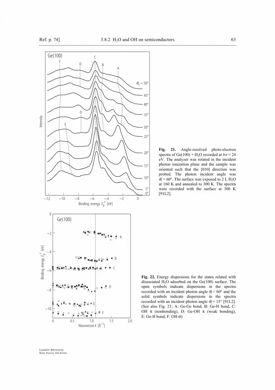
Ref. p. 74] 3.8.2 H2O and OH on semiconductors 63
Landolt-Börnstein New Series III/42A4
Inte
nsity
Ge(100)
− 6 − 4−10 −8 −2−12 0Binding energy [eV]EB
F
D
E
F D BA
C
e = 50°
45°
40°
35°
30°
25°
20°
15°
10°
5°0°
�
Fig. 21. Angle-resolved photo-electron spectra of Ge(100) + H2O recorded at hν = 24 eV. The analyzer was rotated in the incident photon ionization plane and the sample was oriented such that the [010] direction was probed. The photon incident angle was θi = 60°. The surface was exposed to 2 L H2O at 160 K and annealed to 300 K. The spectra were recorded with the surface at 300 K [91L2].
Ge(100)
− 6
− 4
−10
−8
−2
0
Bind
ing
ene
rgy
[eV]
E BF
E
F
D
B
A
C
0 0.5 1.0 1.5 2.0Wavevector [Å ]k −1
Fig. 22. Energy dispersions for the states related with dissociated H2O adsorbed on the Ge(100) surface. The open symbols indicate dispersions in the spectra recorded with an incident photon angle θi = 60° and the solid symbols indicate dispersions in the spectra recorded with an incident photon angle θi = 15° [91L2]. (See also Fig. 21; A: Ge-Ge bond, B: Ge-H bond, C: OH π (nonbonding), D: Ge-OH π (weak bonding), E: Ge-H bond, F: OH σ)

64 3.8.2 H2O and OH on semiconductors [Ref. p. 74
Landolt-Börnstein New Series III/42A4
Inte
nsity
Ge(111)
−15 −10−10 −5 −5−15 0 0
Binding energy [eV]EBVBM
×0.4
×0.4
a1
b 1
b 2
D
C
B
A
D-A
C-A
B-Aa b
Fig. 23. Photoelectron spectra of H2O on Ge(111) at 110 K. a: Original spectra of the clean surface (A), exposed to 0.3 L (B), 1 L (C) and 3 L water (D). The intensities are scaled relative to the intensity of the clean surface spectrum (A). (b) Difference curves (covered minus clean surface spectra) [87K3].
Inte
nsity
GaAs(110)
Binding energy [eV]EBVBM
15 10 5 0
H O:2 1b11b2 3a1
1.5 L
1.2 L
1.0 L
0.8 L
0.6 L
0.4 L
0.2 L
GaAs(110) cleaved
Fig. 24. SXP valence band spectra of H2O adsorbed onto GaAs(110) surface at 100 K. The marks at 0.4 L H2O indicate As-H and Ga-OH bonds [97H]. Fig. 25. see next page

Ref. p. 74] 3.8.2 H2O and OH on semiconductors 65
Landolt-Börnstein New Series III/42A4
Inte
nsity
InSe/H O2
Binding energy [eV]EBF
H O [L]21b1
1b2
3a1
10 L
10 L
−20 −15 −10 −5 EF
In4d
Se pzcleaved
cleaved
cleaved
106.04.02.51.51.00.60.30.20.1
Fig. 26. SXP valence band spectra of water adsorbed onto InSe(0001) surface at 100 K [93M].
Inte
nsity
InP(110)
Binding energy [eV]EBVBM
12 8 4 0
H O:2 1b11b2 3a1
1.3 L
0.3 L
0 L
0.1 L
0.6 L
0.4 L
0.2 L
-P-H -In-OH -P-H -In-OH
Fig. 25. SXP valence band spectra of cleaved InP(110) with increasing H2O dosage at 100 K. Excitation energy 41 eV. The marks at 0.4 L H2O indicate In-OH and P-H bonds [00H].

66 3.8.2 H2O and OH on semiconductors [Ref. p. 74
Landolt-Börnstein New Series III/42A4
Inte
nsity
Vicial Si(100)
Binding energy [eV]EB
a
b
c
3 2 1 0 −1
B
B
B
S 3 S1
S1
S1
S2S4
S4
S 3
H
Fig. 27. (a) Si 2p core level photoemission spectrum recorded at a bulk-sensitive photon energy of hν = 112 eV for the clean Si(100) surface. The energy scale is in binding energy referenced to the bulk Si 2p3/2 component. The solid lines denote a fit with five spin-orbit doublets S1, B, S2, S3 and S4. (b) As in (a), but at a surface-sensitive photon energy hν = 130 eV. (c) Si 2p spectrum as in (b) after exposure to saturation coverage of 2 L of H2O. The new peak labelled H is attributed to emission from Si atoms bonded to H [88M].
Figures 28 - 30, see next pages
Inte
nsity
Si(111)
Binding energy [eV]EB
102 100 98 536 533 530
534.6
534
532.6
99.7
×1×1
×1 ×1
×1/3
H O saturat.300 K
2
Exposure [L]L
10
5
2
1
0.4
0.2
0
Fig. 31. Si 2p (left) and O 1s (right) X-ray photoelectron spectra for water adsorbed on Si(111)2×1 [85S].

Ref. p. 74] 3.8.2 H2O and OH on semiconductors 67
Landolt-Börnstein New Series III/42A4
Inte
nsity
Si(001)
Binding energy [eV]EB
3 2 1 0 −1 −2
40
20
0
40
40
40
40
20
20
20
20
0
0
0
0
1+
2+3+
4+80 L
20 L
5 L
1 L
0 L
3+2+
2+
1+
1+
1+
Si-H
Si-H
Si-H
O.D.A.
4
A
Fig. 28. Si 2p3/2 spectra (peak maxima normalized to 100) of the Si(001) surface exposed at 90 K to increasing water exposures. The vapor pressure was 2×10⁻⁸ Torr for the first two exposures and 5×10⁻⁸ Torr for the last three ones. Curve reconstructions are also given, a SiH contribution (dashed line) at about +0.3 eV is introduced for the best resolved spectra [95P]. (1+, 2+ etc. denote the different oxidation states of Si; ODA contribution, dotted line, of outer dimer atoms, A not defined by authors).

68 3.8.2 H2O and OH on semiconductors [Ref. p. 74
Landolt-Börnstein New Series III/42A4
Inte
nsity
Si(001)
Binding energy [eV]EB
3 2 1 0 −1 −2
40
20
0
40
40
40
40
20
20
20
20
0
0
0
0
40 L
20 L
5 L
1 L
0 L
2+
1+
1+
O.D.A.
4
A
Fig. 29. Si 2p3/2 spectra (peak maxima normalized to 100, EB is given relative to bulk Si 2p3/2) of the Si(001)2×1 surface exposed at 300 K to increasing water exposures (under 2×10⁻⁸ Torr). Curve reconstructions are also given [95P]. (1+, 2+ denote the different oxidation states of Si; ODA contribution, dotted curve, of outer dimer atoms, A not defined by authors).

Ref. p. 74] 3.8.2 H2O and OH on semiconductors 69
Landolt-Börnstein New Series III/42A4
Inte
nsity
Si(111)
Binding energy [eV]EB
3 2 1 0 −1 −2
4040
2020
00
4+
80 L
20 L
5 L
10 L
0 L
2+
1+
1+
4
×5
×5
40
40
40
4040
20
20
20
2020
0
0
0
00
40
40
20
20
0
0
A2
A1
RA
40 L
60 L
Fig. 30. Si 2p3/2 spectra (peak maxima normalized to 100, EB is given relative to bulk Si 2p3/2) of the Si(111)7×7 surface exposed at 300 K to increasing water exposures (under 5×10⁻⁸ Torr). Curve reconstructions are also given [95P]. (RA: rest atom, A1: Si-adatoms, A2: not defined by authors, +1, +2, etc. denote the different oxidation states of Si).

70 3.8.2 H2O and OH on semiconductors [Ref. p. 74
Landolt-Börnstein New Series III/42A4
Inte
nsity
Ge(100)
Binding energy [eV]EB
2 1 0 −1
a
b
c
Fig. 32. Ge(100) 3d core-level spectra recorded at 70 eV photon energy. The filled circles show the raw data after background subtraction and the lines show the calculated fits to the data: (a) the spectrum from the clean surface recorded at 300 K, (b) the spectrum from the surface after a 1 L H2O exposure at 160 K, and (c) the spectrum from the surface after a 1 L H2O exposure at 160 K and heating to 300 K. The binding energy is referred to the bulk Ge 3d5/2 components [89L].
Inte
nsity
Inte
nsity
WSe2
Binding energy [eV]EB Binding energy [eV]EB
−24 −24−26 −26−28 −28
a b
2a1
2a1H O-expose
[L]2
3.5
1.50.5
0
−30 −30−22 −22
162 K
150 K
120 K
Fig. 33. H2O adsorption on WSe2 (0001) at 120 K. SXP spectra of the O 2s level as function of coverage during adsorption (a) and during desorption, after 3.5 L H2O-exposure (b) [93M].

Ref. p. 74] 3.8.2 H2O and OH on semiconductors 71
Landolt-Börnstein New Series III/42A4
Inte
nsity
Si(100)
Energy loss [cm ]Eloss−1
820
2090
37001640630
840650
480 1520
2090 2700
90
0 1000 3000 40002000
×1000
×300
×80
×2000
×2000
×800 1L H O2
1L D O2
10−2
10−3
0.1 1
Si-OH
SiH ×10( )
Exposure [10 Torr s]L −6
Rel.
inte
nsity
Fig. 34. Electron energy loss spectra of 1 L of H2O and D2O, respectively, on a Si(100) surface at 300 K. The loss at 1640 cm-1 in the upper spectrum is a double loss of 820 cm-1. The 2090 cm-1 loss on the D2O exposed surface is produced through some H-D-exchange or H2O contamination. The electron impact energy was 14 eV. The insert displays the intensities of the 820 cm-1 loss and the 2090 cm-1 (SiH) loss vs coverage [82I2].
Rela
tive
refle
ctiv
ityR
/R
1700 2000 2300 2600 2900 3200 3500Frequency [cm ]−1
a
b
c
d
×1
×1
×0.67
×1
Si(100)P- polarization
∆R / = 4×10R −4
�
�
Fig. 35. Water-induced infrared reflection spectra, ∆R/R, upon water exposure on clean Si(100)2×1 at 80 K: a, 0.5 L with TS = 80 K; b, 0.5 L with TS = 80 K and after annealing to 285 K for 1 min with no additional water exposure; c, 10 L with TS = 80 K; and d, 10 L with TS = 80 K and after annealing to 280 K for 1 min [84C2].

72 3.8.2 H2O and OH on semiconductors [Ref. p. 74
Landolt-Börnstein New Series III/42A4
Frequency [cm ]−1
Si(100)
2×10⁻³
600 800 1000 1200 1400 1600
Abso
rban
ce
840 cmSi-OD stretch
−1
825 cmSi-OH stretch
−1
898 cmSiOH bend
−1
1517 cmSi-D stretch
−1658 cmSiOD bend
−1
a D O2
b H O216
5×10⁻⁴
Abso
rban
ce
2085 cmSi-H stretch
−1
2000 2100Frequency [cm ]−1
�
�
Fig. 36. Infrared absorption spectra of Si(100) surfaces after 2 L exposures to (a) D2O and (b) 16
2H O at ~300 K [97S3].
Inte
nsity
Si(111)
Energy loss [cm ]Eloss−1
810 2090
3680630 9503420
90
0 1000 30002000
×1000
×100
×18
×2500
a
b
Fig. 37. Electron energy loss spectra of (a) 2L of H2O condensed on a Si(111)7×7 surface held at 100 K. (b) The same surface after annealing briefly to 300 K [82I2].
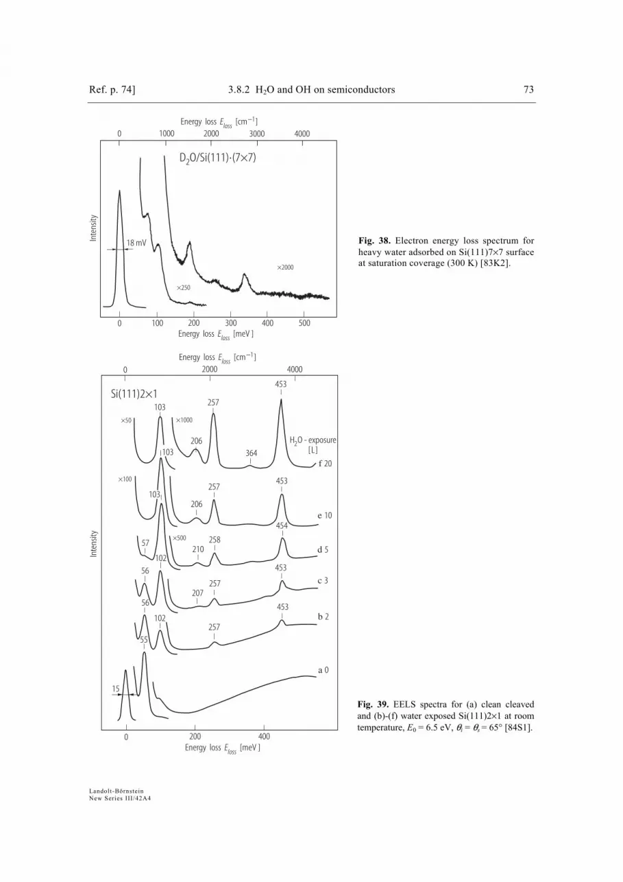
Ref. p. 74] 3.8.2 H2O and OH on semiconductors 73
Landolt-Börnstein New Series III/42A4
Inte
nsity
D O/Si(111) (7×72 ⋅
Energy loss [meV ]Eloss
Energy loss [cm ]Eloss−1
18 mV
×2000
×250
)
0 1000 2000 3000 4000
0 100 200 300 400 500
Fig. 38. Electron energy loss spectrum for heavy water adsorbed on Si(111)7×7 surface at saturation coverage (300 K) [83K2].
Inte
nsity
Si(111)2×1
Energy loss [meV ]Eloss
Energy loss [cm ]Eloss−1
15
×1000
×500
×100
×50
0 2000 4000
0 200 400
103 257
453
103206
364
453
454
453
453
103257
206
258210
57
102
56
207257
257102
56
55
H O - exposure[L]
2
f 20
e 10
d 5
c 3
b 2
a 0
Fig. 39. EELS spectra for (a) clean cleaved and (b)-(f) water exposed Si(111)2×1 at room temperature, E0 = 6.5 eV, θi = θs = 65° [84S1].

74 3.8.2 H2O and OH on semiconductors
Landolt-Börnstein New Series III/42A4
References for 3.8.2
55H Hauffe, K.: Advanced Catalysis 7 (1955) 213. 57K Kisliuk, P.J.: J. Phys. Chem. Solids 3 (1957) 95. 58K Kisliuk: J. Phys. Chem. Solids 5 (1958) 78. 63W Wolkenstein, T., The Electron Theory of Catalysis on Semiconductors, (Pergamon Press,
Oxford, 1963). 68E Ertl, G.: Ber. Bunsenges. Phys. Chem. 72 (1968) 74. 71M Meyer, F.: Surf. Sci. 27 (1971) 107. 73H Henzler, M.,Töpler, J.: Surf. Sci. 40 (1973) 388. 75F Fujiwara, K.,Nishijima, M.: Phys. Lett. 55A (1975) 211. 75S Sinharoy, S.,Henzler, M.: Surf. Sci. 51 (1975) 75. 75Y Yu, K.Y., McMenamin, J.C.,Spicer, W.E.: Surf. Sci. 50 (1975) 149. 77F Fujiwara, K.,Ogata, H.: J. Appl. Phys. 48 (1977) 4360. 77M Morrison, S.R., The Chemical Physics of Surfaces, (Plenum Press, New York, 1977). 79B Büchel, M.,Lüth, H.: Surf. Sci. 87 (1979) 285. 79F Fujiwara, K.,Ogata, H.: Surf. Sci. 86 (1979) 700. 79G Galaev, A.A., Gamosov, L.V., Parkhomenko, Y.N.,Shirkov, A.V.: Sov. Phys. Crystallogr. 24
(1979) 72. 81F1 Fujiwara, K.: Surf. Sci. 108 (1981) 124. 81F2 Fujiwara, K.: Journal of Chemical Physics 75 (1981) 5172. 81T Thornton, G., Rosenberg, R.A., Rehn, V., Green, A.K.,Parks, C.C.: Solid St. Commun. 40
(1981) 131. 82G Gmelin, Handbook of Inorganic Chemistry, H. Koschel ed. ed., (Springer Verlag, 1982). 82I1 Ibach, H., Bruchmann, D.,Wagner, H.: Appl. Phys. A 29 (1982) 113. 82I2 Ibach, H., Wagner, H.,Bruchman, D.: Solid St. Commun. 42 (1982) 457. 82M Montgomery, V.,Williams, R.H.: J. Phys. C 15 (1982) 5887. 82W Webb, C.,Lichtensteiger, M.: J. Vac. Sci. Technol. 21 (1982) 659. 83B Black, J.E., Bopp, P.,Wolfsberg, M.: Surf. Sci. 134 (1983) 257. 83C1 Ciraci, S., Erkoc, S.,Ellialioglu, S.: Solid St. Commun. 45 (1983) 35. 83C2 Ciraci, S.,Wagner, H.: Phys. Rev. B 27 (1983) 5180. 83K1 Kahn, A.: Surf. Sci. Rep. 3 (1983) 193. 83K2 Kobayashi, H., Kubota, T., Onchi, M.,Nishijima, M.: Phys. Lett. 95A (1983) 345. 83S1 Schmeisser, D., Himpsel, F.J., Holliger, G., Reihl, B.,Jacobi, K.: Phys. Rev. B 27 (1983) 3279. 83S2 Schmeisser, D., Himpsel, F.J., Hollinger, G.,Reihl, B.: Phys. Rev. B 27 (1983) 7813. 84C1 Chabal, Y.J.: Phys. Rev. B 29 (1984) 3677. 84C2 Chabal, Y.J.,Christman, S.B.: Phys. Rev. B 29 (1984) 6974. 84C3 Childs, K.D., Luo, W.-A.,Lagally, M.G.: J. Vac. Sci. Technol. A 2 (1984) 593. 84M Mokwa, W., Kohl, D.,Heiland, G.: Surf. Sci. 139 (1984) 98. 84O Oellig, E.M., Butz, R., Wagner, H.,Ibach, H.: Solid St. Commun. 51 (1984) 7. 84S1 Schaefer, J.A., Stucki, F., Frankel, D.J., Göpel, W.,Lapeyre, G.J.: J. Vac. Sci. Technol. B 3
(1984) 359. 84S2 Schmeisser, D.: Surf. Sci. 137 (1984) 197. 84S3 Stucki, F., Anderson, J., Lapeyre, G.J.,Farrell, H.H.: Surf. Sci. 143 (1984) 84. 85C Chabal, Y.J.: J. Vac. Sci. Technol. A 3 (1985) 1448. 85N Nishijima, M., Edamota, K., Kobayashi, H.,Onchi, M.: Surf. Sci. 158 (1985) 422. 85R1 Ranke, W.,D.Schmeisser: Surf. Sci. 149 (1985) 485. 85R2 Ranke, W., Schmeisser, D.,Xing, Y.R.: Surf. Sci. 152/153 (1985) 1103. 85R3 Ranke, W.,Xing, Y.R.: Surf. Sci. 157 (1985) 339. 85S Schäfer, J.A., Anderson, J.,Lapeyre, G.J.: J. Vac. Sci. Technol. A 3 (1985) 1443. 85T Takayanagi, K., Tonishiro, Y., Takahashi, M.,Takahashi, S.: J. Vac. Sci. Technol. A 3 (1985)
1502. 86B Broughton, J.Q., Schaefer, J.A., Bean, J.C.,Farrel, H.H.: Phys. Rev. B 33 (1986) 6841. 86N Nishijima, M., Edamoto, K., Kubota, Y., Tanaka, S.,Onchi, M.: J. Chem. Phys 84 (1986) 6458.

3.8.2 H2O and OH on semiconductors 75
Landolt-Börnstein New Series III/42A4
86S1 Schaefer, J.A., Anderson, J.,Lapeyre, G.J.: J. Electr. Spectr. Rel. Phen. 38 (1986) 21. 86S2 Schmeisser, D.,Demuth, J.E.: Phys. Rev. B (1986) 4233. 87B Barone, V., Lelj, F., Russo, N.,Toscano, M.: Journal de chimie physique 84 (1987) 5. 87F Feenstra, R.M., Strodcio, J.A.,Fein, A.P.: Surf. Sci. 181 (1987) 295. 87J Jaegermann, W.,Schmeisser, D.: J. Vac. Sci. Technol. A 5 (1987) 627. 87K1 Katircioglu, S.: Surf. Sci. 187 (1987) 569. 87K2 Kuhr, H.J.,Ranke, W.: Surf. Sci. 189/190 (1987) 420. 87K3 Kuhr, H.J.,Ranke, W.: Surf. Sci. 187 (1987) 98. 87L1 Larsson, C.U.S., Flodström, A.S., Nyholm, R., Incoccia, L.,Senf, F.: J. Vac. Sci. Technol. A 5
(1987) 3321. 87L2 Larsson, C.U.S., Johnson, A.L., Flodström, A.,Madey, T.E.: J. Vac. Sci. Technol. A 5 (1987)
842. 87R Russo, N.,Toscano, M.: Surf. Sci. 180 (1987) 599. 87T Thiel, P.A.,Madey, P.E.: Surf. Sci. Rep. 7 (1987) 211. 88D Dong, G., Ding, X., Hou, X.,Wang, X.: Surf. Sci. 201 (1988) 531. 88F Froitzheim, H., in: The Chemical Physics of Solid Surfaces and Heterogeneous Catalysis, Vol. 5,
Eds. D. A. King, D. P. Woodruff, (Elsevier, Amsterdam, 1988), pp. 183. 88H Hansson, J.G.V.,Uhrberg, R.I.G.: Surf. Sci. Rep. 9 (1988) 197. 88J Jaegermann, W.,Tributsch, H., in: Progress in Surface Sciences, Vol. 29, Ed. S. G. Davison,
(Pergamon Press, New York, 1988), p. 1. 88M McGrath, R., Cimino, R., Braun, W., Thornton, G.,McGovern, I.T.: Vacuum 38 (1988) 251. 89F Fives, K., McGrath, R., Stephens, C., McGovern, I.T., Cimino, R., Law, D.S.-L., Johnson,
A.L.,Thornton, G.: J. Phys.: Condens. Matter 1 (1989) SB105. 89H Hamers, R.J.,Köhler, U.K.: J. Vac. Sci. Technol. A 7 (1989) 2854. 89K Koehler, B.G., Mak, C.H.,George, S.M.: Surf. Sci. 221 (1989) 565. 89L Larsson, C.U.S., Flodström, A.S., Karlsson, U.O.,Yang, Y.: J. Vac. Sci. Technol. A 7 (1989)
2044. 89O Ong, C.K.: Solid St. Commun. 72 (1989) 1141. 89P1 Papagno, L., Caputi, L.S., Anderson, J.,Lapeyre, C.J.: Phys. Rev. B 40 (1989) 8443. 89P2 Payne, M.C., Roberts, N., Needs, R.J., Needels, M., Joannopoulos, J.D.,al, e.: Surface Science
211/212 (1989) 1. 89S Seebauer, E.G.: J. Vac. Sci. Technol. A 7 (1989) 3279. 90E Engler, C.: phys. stat. sol. (b) 159 (1990) 721. 90S Schröder-Bergen, E.,Ranke, W.: Surf. Sci. 236 (1990) 103. 91A Avouris, P.,Lyo, I.: Surf. Sci. 242 (1991) 1. 91L1 Larsson, C.U.S.,Flodström, A.S.: Vacuum 42 (1991) 297. 91L2 Larsson, C.U.S.,Flodström, A.S.: Phys. Rev. B 43 (1991) 9281. 91P1 Papagno, L., Frankel, D., Chen, Y., Caputi, L.S., Anderson, J.,Lapeyre, G.J.: Surf. Sci. 248
(1991) 343. 91P2 Pettenkofer, C., Jaegermann, W.,Bronold, M.: Ber. Bunsenges. Phys. Chem. 95 (1991) 560. 91P3 Podolsky, B.S., Ukraintsev, V.A.,Chernov, A.A.: Surf. Sci. 251/252 (1991) 1033. 91P4 Podolsky, B.S., Ukraintsev, V.A.,Chernov, A.A.: Sov. Phys. Solid State 33 (1991) 65. 91S Shao, Y.,Paul, J.: Vacuum 42 (1991) 313. 91U Ukraintsev, V.A., Podolsky, B.S.,Chernov, A.A.: Appl. Surf. Sci. 48/49 (1991) 151. 92B Brillson, L.J., Handbook of Semiconductors, Vol. I, North Holland, 1992). 92C Cohen, S.M., Yang, Y.L., Rouchance, E., Jin, T.,D´Evelyn, M.D.: J. Vac. Sci. Technol. A 10
(1992) 2166. 92D Dai, D., Zhu, F., Luo, Y.,Davoli, I.: J. Phys.: Condens. Matter 4 (1992) 5855. 92L Landemark, E., Karlsson, C.J., Chao, Y.-C.,Uhrberg, R.I.G.: Phys. Rev. Lett. 69 (1992) 1588. 92M Mayer, T., Klein, A., Lang, O., Pettenkofer, C.,Jaegermann, W.: Surf. Sci. 269/270 (1992) 909. 92S Sander, M., Jaegermann, W.,Lewerenz, H.J.: J. Phys. Chem. 96 (1992) 782. 92W Wolkow, R.A.: Phys. Rev. Lett. 27 (1992) 2636. 93A Andersohn, L.,Köhler, U.: Surf. Sci. 284 (1993) 77. 93C1 Carlson, C.R., Buechter, W.F., Che-Ibrahim, F.,Seebauer, E.G.: J. Chem. Phys 99 (1993) 7190.

76 3.8.2 H2O and OH on semiconductors
Landolt-Börnstein New Series III/42A4
93C2 Chander, M., Li, Y.Z., Patrin, J.C.,Weaver, J.H.: Phys. Rev. B 48 (1993) 2493. 93J K. Jacobi, U.M.: Surf. Sci. 284 (1993) 223. 93L Lacharme, J.P., C. Sébenne, Chérif, S.M., Safta, N.,Zaibi, M.A.: Appl. Surf. Sci. 65/66 (1993)
598. 93M Mayer, T.: Ph.D. Thesis, Technische Universität Berlin, 1993. 93R1 Ranke, W.: J. Electr. Spectr. Rel. Phen. 61 (1993) 231. 93R2 Ranke, W.,Wasserfall, J.: Surf. Sci. 292 (1993) 10. 94B Bu, H.,Rabalais, J.W.: Surf. Sci. 301 (1994) 285. 94G Gao, Q., Z. Dohnalek, Cheng, C.C., W.J. Choyke,J.T. Yates, J.: Surf. Sci. 312 (1994) 261. 94H Himpsel, F.H., in: Handbook of Semiconductors, Vol. II, Eds. T. S. Moss, M. Balkowski,
Amsterdam, 1994), pp. 161 . 94K Karlsson, C.J., Landemark, E., Chao, Y.-C.,Uhrberg, R.I.G.: Phys. Rev. B 50 (1994) 5767. 94L Lay, G.l., Göthelid, M., Grekh, T.-M., Björkquist, M., Karlsson, K.O.,Aristov, U.Y.: Phys. Rev.
B 50 (1994) 14277. 94S1 Schulze, R.K.,Evans, J.F.: Appl. Surf. Sci. 81 (1994) 449. 94S2 Sebenne, C., in: Handbook of Semiconductors, Vol. II, Eds. T. S. Moss, M. Balkowski,
Amsterdam, 1994), pp. 33 . 95L Lüth, H., in: Surfaces and Interfaces of Solid Materials 3 Ed. Springer-Verlag, Berlin, 1995). 95M Mönch, W., in: Semiconductor Surfaces and Interfaces 2nd ed., (Springer-Verlag, Berlin, 1995). 95P Poncey, C., Rochet, F., Dufour, G., Roulet, H., Sirotti, F.,Panaccione, G.: Surf. Sci. 338 (1995)
143. 95V Vittadini, A., Selloni, A.,Casarin, M.: Phys. Rev. B 52 (1995) 5885. 95W1 Waltenburg, H.N.,Yates, J.T.J.: Chemical Reviews 95 (1995) 1589. 95W2 Wise, M., Okada, L., Sneh, O.,George, S.: J. Vac. Sci. Technol. A 13 (1995) 1853. 96F Flowers, M.C., Jonathan, N.B.H., Morris, A.,Wright, S.: Surf. Sci. 351 (1996) 87. 96H Henrion, O., Löher, T., Klein, A., Pettenkofer, C.,Jaegermann, W.: Surf. Sci. 366 (1996) L685. 96I Ikeda, H., Yamada, T., Hotta, K., Zaima, S.,Yasuda, Y.: Appl. Surf. Sci. 100/101 (1996) 431. 96J Jaegermann, W., in: Modern Aspects of Electrochemistry Ed. R. E. White, New York, 1996). 96K Katircioglu, S.,Ercoc, S.: phys. stat. sol. (b) 196 (1996) 77. 96M Mayer, T., Pettenkofer, C.,Jaegermann, W.: J. Phys. Chem. 100 (1996) 16966. 96R1 Raghavachari, K., Chabal, Y.J.,Struck, L.M.: Chem. Phys. Lett. 252 (1996) 230. 96R2 Ranke, W.: Surf. Sci. 369 (1996) 137. 96R3 Ranke, W.,Xing, Y.R.: Surface Review and Letters 4 (1996) 15. 96R4 Rincón, R., García-Vidal, F.J.,Flores, F.: Appl. Surf. Sci. 92 (1996) 216. 96S1 Scholz, S.M.,Jacobi, K.: Surf. Sci. 369 (1996) 117. 96S2 Sekiguchi, T., Ikeura, H., Tanaka, K.,Obi, K.: J. Electr. Spectr. Rel. Phen. 80 (1996) 65. 96S3 Sloan, D.W., Sun, Y.-M.,White, J.M.: J. Vac. Sci. Technol. A 14 (1996) 216. 97E Ezzehar, H., Stauffer, L., Leconte, J.,Minot, C.: Surf. Sci. 388 (1997) 220. 97H Henrion, O.: Ph.D. Thesis, Technische Universität Berlin, 1997. 97K Konecny, R.,Doren, D.J.: Journal of Chemical Physics 106 (1997) 2426. 97M1 Mitchell, W.J., Chung, C.-H., Yi, S.I., Hu, E.L.,Weinberg, W.H.: Surf. Sci. 384 (1997) 81. 97M2 Mitchell, W.J., Chung, C.-H., Yi, S.I., Hu, E.L.,Weinberg, W.H.: J. Vac. Sci. Technol. B 15
(1997) 1182. 97P Piancastelli, M.N., Paggel, I.J., Weindel, C., Hasselblatt, M.,Horn, K.: Phys. Rev. B 56 (1997) R
12737. 97R Ranke, W.,Xing, Y.R.: Surf. Sci. 381 (1997) 1. 97S1 Self, K.W., Yan, C.,Weinberg, W.H.: Surf. Sci. 380 (1997) 408. 97S2 Seshadri, G., Lin, T.-C., Ballinger, A.,Kelber, J.A.: Langmuir 13 (1997) 3219. 97S3 Struck, L.M., Jr., J.E., Bent, B.E., Flynn, G.W., Chabal, Y.J., Christman, S.B., Chaban, E.E.,
K.Raghavachari, Williams, G.P., Radermacher, K.,Mantl, S.: Surf. Sci. 380 (1997) 444. 97W Weldon, M., Stefanov, B., Raghavachari, K.,Chabal, Y.J.: Phys. Rev. Lett. 79 (1997) 2851. 97Z Zaibi, M.A., Lacharme, J.P.,Sebénne, C.A.: Surf. Sci. 377-379 (1997) 639. 98C Chung, C.-H., Yi, S.I.,Weinberg, W.H.: J. Vac. Sci. Technol. A 16 (1998) 1785.

3.8.2 H2O and OH on semiconductors 77
Landolt-Börnstein New Series III/42A4
98F Franco, N., Chrost, J., Avila, J., Müller, C., Dudzik, E., Patchett, A.J., McGovern, I.T., Giebel, T., Lindsay, R., Fritsche, V., Bradshaw, A.M.,Woodruff, D.P.: Appl. Surf. Sci. 123/124 (1998) 219.
00H Henrion, O., Klein, A.,Jaegermann, W.: Surf. Sci. 457 (2000) L337.