Embed Size (px)
Citation preview

Seediscussions,stats,andauthorprofilesforthispublicationat:https://www.researchgate.net/publication/258452596
3Dheteroepitaxyofmismatchedsemiconductorsonsilicon
ARTICLEinTHINSOLIDFILMS·APRIL2014
ImpactFactor:1.76·DOI:10.1016/j.tsf.2013.10.094
CITATION
1
READS
71
16AUTHORS,INCLUDING:
ClaudiuV.Falub
ETHZurich
92PUBLICATIONS599CITATIONS
SEEPROFILE
ElisabethMüller
PaulScherrerInstitut
176PUBLICATIONS3,368CITATIONS
SEEPROFILE
GiovanniIsella
PolitecnicodiMilano
300PUBLICATIONS2,072CITATIONS
SEEPROFILE
HansvonKaenel
ETHZurich
355PUBLICATIONS5,534CITATIONS
SEEPROFILE
Availablefrom:AntoniaNeels
Retrievedon:03February2016

Thin Solid Films 557 (2014) 42–49
Contents lists available at ScienceDirect
Thin Solid Films
j ourna l homepage: www.e lsev ie r .com/ locate / ts f
3D heteroepitaxy of mismatched semiconductors on silicon
Claudiu V. Falub a,⁎, Thomas Kreiliger a, Fabio Isa b, Alfonso G. Taboada a, Mojmír Meduňa c,d, Fabio Pezzoli e,Roberto Bergamaschini e, Anna Marzegalli e, Elisabeth Müller f, Daniel Chrastina b, Giovanni Isella b,Antonia Neels g, Philippe Niedermann g, Alex Dommann g,1, Leo Miglio e, Hans von Känel a
a Laboratory for Solid State Physics, ETH-Zürich, Schafmattstrasse 16, 8093 Zürich, Switzerlandb L-NESS, Department of Physics, Politecnico di Milano, via Anzani 42, 22100 Como, Italyc Department of Condensed Matter Physics, Masaryk University, Kotlářská 2, 61137 Brno, Czech Republicd CEITEC, Masaryk University, Kamenice 5, 60177 Brno, Czech Republice L-NESS, Department of Materials Science, Università degli studi di Milano-Bicocca, via Cozzi 53, 20125 Milano, Italyf Electron Microscopy ETH-Zürich (EMEZ), Schafmattstrasse 16, 8093 Zürich, Switzerlandg Centre Suisse d'Electronique et Microtechnique, Jaquet-Droz 1, 2002 Neuchatel, Switzerland
⁎ Corresponding author at: OC Oerlikon Advanced TecBalzers, Liechtenstein. Tel.: +41 44 633 2261; fax: +41 4
E-mail addresses: [email protected], vkaenel@phys1 Present address: EMPA-Swiss Federal Laboratori
Technology, Lerchenfeldstrasse 5, CH-9014 St. Gallen.
0040-6090/$ – see front matter © 2013 Elsevier B.V. All rihttp://dx.doi.org/10.1016/j.tsf.2013.10.094
a b s t r a c t
a r t i c l e i n f oAvailable online 28 October 2013
Keywords:Monolithic integrationEpitaxial growthGeGaAsPatterned Si substratesScanning X-ray nano-diffractionRoom-temperature photoluminescenceX-ray detectors
We present a method for monolithically integrating mismatched semiconductor materials with Si, coined three-dimensional (3D) heteroepitaxy. The method comprises the replacement of conventional, continuous epilayersby dense arrays of strain- and defect-free, micron-sized crystals. The crystals are formed by a combination ofdeep-patterning of the Si substrates and self-limited lateral expansionduring the epitaxial growth. Consequently,the longstanding issues of crack formation and wafer bowing can be avoided. Moreover, threading dislocationscan be eliminated by appropriately choosing pattern sizes, layer thicknesses and surface morphology, thelatter being dependent on the growth temperature.We show this approach to be valid for various material com-binations, pattern geometries and substrate orientations. We demonstrate that Ge crystals evolve into perfectstructures away from the heavily dislocated interface with Si, by using a synchrotron X-ray beam focused to aspot a few hundred nanometers in size and by recording 3D reciprocal space maps along their height. Roomtemperature photoluminescence (PL) experiments reveal that the interband integrated PL intensity of the Gecrystals is enhanced by almost three orders of magnitude with respect to that of Ge epilayers directly grownon flat Si substrates. Electrical measurements performed on single heterojunction diodes formed between 3DGe crystals and the Si substrate exhibit rectifying behavior with dark currents of the order of 1 mA/cm2. ForGaAs the thermal strain relaxation as a function of pattern size is similar to that found for group IV materials.Significant differences exist, however, in the evolution of crystal morphology with pattern size, which moreand more tends to a pyramidal shape defined by stable {111} facets with decreasing width of the Si pillars.
© 2013 Elsevier B.V. All rights reserved.
1. Introduction
Attempts to extend Moore's Law [1] by introducing additional opti-cal and electrical functionalities to the complementary metal-oxide-semiconductor (CMOS) platform, realization of high-efficiency solidstate lighting, manufacturing of concentrator photovoltaic cells, andthe fabrication of imaging detectors, especially for high-energy electro-magnetic radiation, all require – in one formor another – the integrationof crystalline materials with dissimilar lattice parameters on top ofeach other. Basically, this can be done either by a hybrid approach
hnologies, Iramali 18, FL-94964 633 1072..ethz.ch (C.V. Falub).es for Materials Science and
ghts reserved.
(e.g. various forms of wafer bonding and bump bonding techniques),or by heteroepitaxial growth.
In the case of hybrid technologies, reliability and costs are seriousobstacles for their application on a large scale. That is because differentthermal expansion coefficients induce mechanical stress, which maycause layer cracking and debonding of the wafers [2]. Moreover, forhighly complex systems (e.g. imaging detectors), millions of separatecomponents (e. g. pixels) have to be bump-bonded onto a wafer(e.g. CMOS processed read-out chip) [3].
When two dissimilar materials are combined by heteroepitaxialgrowth, mechanical stress may form as a result of different latticeparameters. When exceeding a certain thickness limit, this misfit stressis relieved either by elastic or plastic relaxation [4,5]. In the case of largemisfit, initial stress relaxation usually occurs elastically by means ofsurface corrugation, for example in the form of islands [6]. For lowermisfit, an epitaxial filmmay remainflat,while stress starts to be relievedplastically bymisfit dislocations (MDs) at a certain critical film thickness

43C.V. Falub et al. / Thin Solid Films 557 (2014) 42–49
[7]. MDs are usually accompanied by threading dislocations (TDs) ex-tending to the surface of the growing film [8]. Both MDs and TDs needto be spatially separated from the active region of a device, since theymay degrade its performance to a large extent. While for finite misfitand sufficient layer thickness MDs always occur, threading dislocationdensities (TDD) can be manipulated by various means.
There have been many approaches to lower TDD in blanket films[9–15].While being partially successful, none of thesemethods resultedin a TDD below 106–107 cm−2 even for a simple system, such asGe/Si(001) with a misfit of 4%.
It was realized long ago that a significant further reduction ofTDDs can only be achieved by reducing the epitaxial growth area,i.e., by making the epitaxial structures small [16]. This can be done bydepositing the epitaxial layers onto small substrate mesas (e.g. pillars)[17,18] or selectively into dielectric windows [19,20] previously definedby lithography and etching. The idea behind this is that with sufficientlayer thickness, threading arms arising from the interface will exitthe sides of the epitaxial structure, rather than reaching the uppersurface. The concept was applied to various semiconductor combina-tions, such as Si, Ge, III–V and II–VI materials. It has become knownunder the name of “aspect ratio trapping (ART)” [20]. This methodseems to work well for dielectric windows of submicron size, as longas neighboring epitaxial patches do not coalesce by lateral overgrowthof the mask. Once a continuous layer starts to form, however, disloca-tion densities again multiply by orders of magnitude. Moreover, uponcoalescence and increasing film thickness, the problems of waferbowing and layer cracking are bound to occur as a result of mismatchedthermal expansion coefficients. The same may happen whenever acontinuous film is cooled to room temperature after the epitaxialgrowth, seriously hampering subsequent processing steps, such asphotolithography and patterning, or also further epitaxial growth [21].These are serious problems when devices require layers with relativelylarge thicknesses, such as high-brightness light emitting diodes, multi-ple junction solar cells, or power transistors.
The problem of wafer bowing has been addressed in variousways inthe past [22–24]. Unfortunately, however, reducing wafer bowing mayeven increase the tendency of layers to crack, because wafer bowing isassociated with elastic stress relief.
Faced with the problem of realizing a low-cost, high-resolution andhigh-efficiency X-ray imaging detector consisting of a very thick Ge ab-sorber layer monolithically integrated on a Si CMOS substrate, we havediscovered away suitable for solving thermal and latticemisfit problemsat a stroke [25]. In order to efficiently absorbharder X-rays, the absorbingGe layer should, however, be exceptionally thick (at least 50 μm), andhave a low defect density to provide dark currents below 1 mA/cm2
for a fully processed device. This challenging task became possible byreplacing continuous semiconductor films tall, closely spaced crystalsseveral microns in width. The method, coined “3D heteroepitaxy”,rests on a combination of deep substrate patterning into tall pillars andself-limited lateral expansion during epitaxial growth. The method hasbeen thoroughly tested for Si1 − xGex alloys grown on Si(001) substrate,for compositions ranging from pure Si to pure Ge [25].
Here, we show that 3D heteroepitaxy can be extended to other ma-terial combinations and substrate orientations, thus providing a concep-tual platform for several device applications. By using scanning X-raynano-diffraction and room temperature photoluminescence we showthat it leads to strain-free, perfect crystals despite a heavily dislocatedinterface. The current–voltage (I–V) characteristics of heterojunctiondiodes formed by individual Ge crystals and the Si substrate exhibit rec-tifying diode behavior with sufficiently low dark currents (b1 mA/cm2)for use in an X-ray detector.
2. Experimental details
Nominal 4″ (001)- and (111)-oriented (within±0.5°), and 6° offcutSi substrates were patterned into arrays of uniformly spaced Si pillars
and ridges by conventional photolithography and deep reactive ionetching (DRIE) based on the Bosch process [26,27]. Etch depths of2 and 8 μm, pillar and ridge base widths ranging from 2 to 40 μm, andtrenchwidths ranging from 1 to 5 μmwere used in this work. Addition-ally, 100 μm thin 6″ CMOS wafers were patterned by the same proce-dure, with readout circuits located on the backside of the wafers. Forelectrical measurements and further device processing the patternedSi substrates were passivated by a ~90 nm thick SiO2 layer apart fromthe top of the Si pillars.
Prior to epitaxial growth, the patterned Si substrates were cleanedusing the standard RCA method. The native oxide was removed bya 5% hydrofluoric acid dip and subsequent rinse in ultrapure water.Once loaded into the growth chamber, the substrates were outgassedin ultra-high vacuum for 15 min at 300 °Cbefore ramping to the growthtemperature. Subsequently, pure Ge and Si1 − xGex alloy crystals weregrown by low-energy plasma-enhanced chemical vapor deposition(LEPECVD) [28] at a rate of ~4 nm/s and temperatures rangingfrom 400 to 600 °C using germane (GeH4) or silane (SiH4) as reactivegases. The base and growth pressures in the chamber were around1 × 10−9 mbar and ~2 × 10⁻² mbar, respectively.
GaAs crystals were grown by metal–organic vapor phase epitaxy(MOVPE) onto 2 μm tall Ge crystals previously deposited on the pat-terned Si substrate by LEPECVD at 495 °C. We have used the standardmethod for the integration of III–V compounds on Si and bulk Ge sub-strates, usually referred to as the two-step growth method [29]. Aftera 7 nm thin, GaAs seed layer grown at 500 °C, GaAs crystalswith heightsranging between 2 and 6 μm were grown onto the Ge/Si structures at680 °C, a growth rate of ~0.5 nm/s and a pressure of ~100 mbar.
The morphology of the Ge, Si1 − xGex and GaAs crystals grown onthe patterned Si substrates was monitored by Nomarski interferencecontrast opticalmicroscopy (Nikon Eclipse 200D) and scanning electronmicroscopy (SEM) (Zeiss ULTRA 55 digital field emission). Crystal cross-sections were performed by means of a dual beam focused ion beam(FIB)/SEM, Zeiss NVision 40with theGa liquidmetal ion source operatedat 30 kV, imaging currents 10 pA, andmilling currents up to 26 nA. Thefacet orientation was determined by atomic force microscopy (AFM)using a XE-100 microscope operated in non-contact mode, and trans-mission and scanning transmission electron microscopy (TEM, STEM)using a Tecnai F30ST TEM/STEM transmission electron microscope(FEI), operated at 300 kV. The specimens for TEM/STEM investigationswere thinned to electron transparency bymechanical thinning followedby Ar-ion milling (4° incidence angle, 4 kV acceleration voltage). Defectetching was used to estimate the dislocation density. The Ge and SiGecrystals were etched for 40 s in a diluted iodine solution at 0 °C, andetch pits were counted by AFM.
High resolution X-ray diffraction (HRXRD) was used to investigatethe crystalline quality and strain of the Ge crystals. Reciprocal spacemaps (RSMs) were recorded in the symmetric (004) and asymmetric(224) or (113) scattering geometries. As laboratory diffractometer weused a PANalytical X'Pert Pro-MRD (Cu Kα1 radiation, beam diameteron the sample of ~1 mm) equipped with a 4-bounce Ge(220) crystalmonochromator on the incident beam, as well as an analyzer crystaland a Xe point detector on the diffracted beam.
To assess the crystalline quality and tilt of individual crystals, scan-ning nano-diffraction experimentswere performed at the ID01 beamlineof the European Synchrotron Radiation Facility (ESRF) in Grenoble witha Huber diffractometer equipped with a high precision piezo (x,y,z)stage. The X-ray beam was focused down to ~300 × 500 nm by meansof Fresnel zone plates. For a certain Bragg reflection, and afixed (x,y) po-sition, the incidence angle of the X-ray beamwas scannedwhilemovingthe beam across the sample. Since a two-dimensional (2D) MAXIPIXpixel detector was used, 3D-RSMs were measured for each (x,y) posi-tion of the X-ray beam on the sample. The RSMs were recorded aroundsymmetric (004) and asymmetric (115) reflections using a beam ener-gy of 11.07 keV. 3D-RSMswere built from rocking scans, varying the in-cidence angle of the focused primary beam impinging the sample. Both

44 C.V. Falub et al. / Thin Solid Films 557 (2014) 42–49
dense crystal arrays and sampleswith isolatedGe crystalswere used forthe nano-diffraction experiments. The sampleswith isolated Ge crystalswere fabricated by etching the dense arrays in 30 wt.% H2O2 solution(90 s at 70 °C) and by removing neighboring crystals using microma-nipulators inside a scanning electron microscope. Reference marks inthe vicinity of the isolated Ge crystals used for nano-diffraction experi-ments were written by means of FIB, so that these crystals could be lo-cated using the optical microscope attached to the diffractometer stage.
(Photoluminescence) PL measurements were carried out at roomtemperature. The samples were excited by a Nd:glass laser. The excita-tion energy was 1.165 eV, the laser spot size on the sample surfaceabout 100 μm, and the resulting power density a few kW/cm2.
3. Results and discussion
3.1. Growth of perfect, 3D epitaxial Ge crystals on Si
Fig. 1(a) shows a perspective SEM view of an array of 8-μm-tall Sipillars fabricated into a Si(001) substrate by DRIE. For 1 μmGe coverage(see the perspective SEM image in Fig. 1(b)) the separation of epitaxialGe crystals is defined by the substrate geometry. The crystals thenexpand both laterally and vertically, but eventually lateral growthquenches (Fig. 1(c)). Surprisingly, the observed self-limited lateralexpansion leaves an air gap between the neighboring crystals of theorder of just several tens of nanometers (Fig. 1(d)), thus preventingtheir coalescence. This results in uniform space-filling (up to 96%) arraysof tall Ge-crystals, typically a few microns in width. As will be shownlater, the tops of these crystals exhibit a mixture of {113}, {111} and(001) facets, depending on the growth temperature.
Fig. 1. Perspective-view SEMmicrograph of: a) 8-μm-tall Si pillars fabricated on Si(001) substrapillars in (a); c) 8-μm-tall Ge crystals grown at 490 °C on top of the Si pillars in (a). d) Dark-fielde) Perspective and f) front view SEM micrograph of ~50-μm-tall Ge crystals grown at 490 °C.patterned and unpatterned areas of ~27-μm-thick Ge film grown at 490 °C on a Si(001) substr
The space-filling arrays of epitaxial crystals obtained by self-limitedlateral growth on top of Si pillars were found to be remarkably indepen-dent of the thickness of the deposit and any detail of the substratepatterns, e.g. patterning periodicity, pillar size and substrate conditions(e.g. oxidemasking). Itwas shown to not evendependon the lattice andthermal mismatch, as pure Si, and Si1 − xGex alloy crystal arraysexhibited self-limited lateral expansion similar to pure Ge [25]. Thus,Ge crystals as tall as 50 μm could be grown as shown in Fig. 1(e) and(f). Since a continuous layer is prevented to form in this way, crackscan neither nucleate nor propagate (Fig. 1(g)), and wafer bending,often precluding further processing, is minimized. The axes of theepitaxial crystals are defined by the growth direction, even when 6°off-cut substrates were used. A similar self-limited lateral growthmode was observed also for Ge deposition on top of patterned Si(111)substrates, as shown in the top view SEM images of arrays of 8-μm-tall Ge crystals in Fig. 2(a) and (b). The Ge crystals grown on Si(111)substrates exhibit threefold symmetry, as shown in detail in Fig. 2(c),where various facets have been identified from the (111) stereographicprojection of a cubic material with the diamond structure, e.g. Si, SiGeand Ge. Self-limited lateral growth was observed also for patternsconsisting of parallel ridges (Fig. 2(d)).
The growth mechanism by which space-filling arrays of 3D crystalsare formedwas explained by short surface diffusion lengths andmutualgeometric shielding of the flux of reactive species by neighboring crys-tals [25]. Short diffusion lengths are well known to favor kinetic andindependent growth conditions for the different crystal facets. For Si,Ge and SiGe alloys diffusion lengths which are short in comparison totypical facet extensions result from the high growth rate typical forLEPECVD (of the order of several nm/s). Compound semiconductors
tes by photolithography and DRIE; b) 1-μm-tall Ge crystals grown at 490 °C on top of the SiSTEM of ~8-μm-tall Ge crystals grown at 440 °C, exhibiting self-limited lateral expansion.g) Nomarski interference contrast micrograph of the region close to the border betweenate showing the crack inhibition in the patterned region.
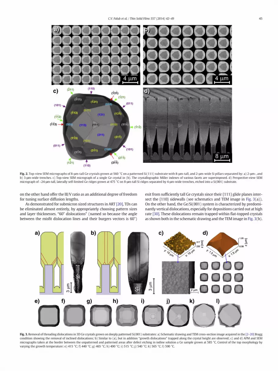
Fig. 2. Top-view SEMmicrographs of 8-μm-tall Ge crystals grown at 560 °C on a patterned Si(111) substrate with 8-μm-tall, and 2-μm-wide Si pillars separated by: a) 2-μm-, andb) 3-μm-wide trenches. c) Top-view SEM micrograph of a single Ge crystal in (b). The crystallographic Miller indexes of various facets are superimposed. d) Perspective-view SEMmicrograph of ~24-μm-tall, laterally self-limited Ge ridges grown at 475 °C on 8-μm-tall Si ridges separated by 4-μm-wide trenches, etched into a Si(001) substrate.
45C.V. Falub et al. / Thin Solid Films 557 (2014) 42–49
on the other hand offer the III/V ratio as an additional degree of freedomfor tuning surface diffusion lengths.
As demonstrated for submicron sized structures in ART [20], TDs canbe eliminated almost entirely, by appropriately choosing pattern sizesand layer thicknesses. “60° dislocations” (named so because the anglebetween the misfit dislocation lines and their burgers vectors is 60°)
Fig. 3.Removal of threading dislocations in 3DGe crystals grown on deeply patterned Si(001) sucondition showing the removal of inclined dislocations; b) Similar to (a), but in addition “gromicrographs taken at the border between the unpatterned and patterned areas after defect etvarying the growth temperature: e) 415 °C; f) 440 °C; g) 465 °C; h) 490 °C; i) 515 °C; j) 540 °
exit from sufficiently tall Ge crystals since their {111} glide planes inter-sect the {110} sidewalls (see schematics and TEM image in Fig. 3(a)).On the other hand, the Ge/Si(001) system is characterized by predomi-nantly vertical dislocations, especially for depositions carried out at highrate [30]. These dislocations remain trapped within flat-topped crystalsas shown both in the schematic drawing and the TEM image in Fig. 3(b).
bstrates: a) Schematic drawing and TEM cross-section image acquired in the [2–20] Braggwth dislocations” trapped along the crystal height are observed; c) and d) AFM and SEMching in iodine solution a Ge sample grown at 585 °C. Control of the top morphology byC; k) 565 °C; l) 590 °C.

46 C.V. Falub et al. / Thin Solid Films 557 (2014) 42–49
They are, however, deflected towards the sidewalls when the growthfront consists of inclined {113} and {111} facets [31]. This can be seenboth from cross-section TEM images [25] and etch pit density measure-ments (Fig. 3(c) and (d)). In unpatterned areas, theGefilm exhibits highdensity of etch pits (~108 cm−2), while none are observed on facettedGe crystals. Themorphology of the Ge crystals can be tuned by carefullyadjusting the growth temperaturewithout jeopardizing the self-limitedlateral expansion. This may be seen from the top view SEM images of(Fig. 3(e–l)). They reveal the facet evolution for growth temperaturesranging from 415 °C to 590 °C. The (001) facet dominating at low tem-peratures progressively shrinks at the expense of various inclined facetsemerging at higher temperatures. The most pronounced of these are{113} facets to which the structures rapidly evolve at temperaturesabove 540 °C. This has been explained by slight variations of relativefacet growth velocities with temperature, which lead to surprisinglylarge changes of the surface morphology [25].
The crystalline quality and strain status of theGe and Si1 − xGex crys-tals were obtained from HRXRD measurements around the Si(004)and Si(224) reflections performed with the laboratory diffractometer.Basically, the diffraction peaks corresponding to the 3D Ge crystalsexhibit two components (see red line in Fig. 4(a)). The intense and
Fig. 4. Analysis of crystal quality of 3D Ge crystals: a) X-ray scans along the Qz direction in thepatterned Si wafer, comparing the patterned and unpatterned regions, and a high-quality Gewaiment. A 11.07 keV is focused by means of Fresnel Zone Plate onto an array of 3D Ge crystals anmeasured in the (115) scattering geometry at the top of an isolated, 11-μm-tall Ge crystal dhave been etched in H2O2 and the surrounding neighboring crystals have been removed by mthe (Qx,Qz) plane. The broad, weaker peak stem from the defectedmaterial in the trenches, whiterial deposited on the Si pillar. f) Perfect single crystals emerging from imperfect interfaces: FWdata are fitted by y(x) = y0 + a ⋅ exp(−b ⋅ x) (red line), where a and b are a positive consta
sharp component, as sharp as the diffraction peak of a high-quality Gewafer (black line in Fig. 4(a)), centered around 4.4421/Å, correspondsto the fully relaxed Ge material deposited on top of the Si pillar. Themuch weaker component, shifted to higher Qz momentum values,stems from the tensile-strained material (~0.11%) deposited betweenthe Si pillars. In the unpatterned regions, the Gematerial is under a ten-sile strain of ~0.14% (blue line in Fig. 4(a)).
Thus, the laboratory HRXRD provided evidence for the nearly per-fect crystal structure of the epitaxial material, and showed the crystalsgrown on the Si pillars to be strain-free. Thermal strain relaxation ispurely elastic, due to the high-aspect ratio of the Ge crystals, as con-firmed by finite element method simulations [25]. In addition tocrystalline quality and strain, another goal of the HRXRD measure-ments was to investigate and understand the effect of the local crystaltilts. Besides the mutual shadowing of neighboring crystals, whichlowers the lateral growth rate at the expense of the vertical growthrate, the random local tilts might be the key to understanding ofhow crystals grow closer and closer together without fusing in spiteof their very large height-to-base ratios. Thus, we have investigatedthe evolution of the crystalline structure and strain at the early stagesof the growth, in order to understand the transition from isolated
vicinity of Ge(004) Bragg reflection for 16-μm-thick Ge material deposited at 440 °C on afer. b) Schematics of the nanodiffraction experiments at the ID01 beamline of ESRF exper-d the diffracted signal is measured by a 2D pixel detector. c) 3D reciprocal space mapping) Perspective-view SEM micrograph of four isolated, 11-μm-tall Ge crystals. The crystalseans of micromanipulators operated inside an SEM. e) Projection of the 3D RSM in (c) onle the superimposed sharp, more intense peak is due to the high-quality crystalline Gema-HM of the Ge(115) peak (ΔQx) along the Qx direction vs. crystal height. The experimental
nts.

47C.V. Falub et al. / Thin Solid Films 557 (2014) 42–49
heterostructures to arrays of closely spaced crystals. In order to mea-sure small lattice tilts for individual pillars, we made use of an intenseX-ray beam focused down to ~300 × 500 nm, small enough to probea single Ge crystal (see Fig. 4(b)). Collection of the diffracted signal bya 2-dimensional MAXIPIX pixel detector permitted the construction of3D-RSMs at each (x,y) position of the X-ray beam on the sample asshown for the reciprocal space region around a (115) reflection inFig. 4(c).
In order to study the tilts of individual Ge crystals without any inter-ference from their closely spaced nearest neighbors, some crystals wereisolated by a combination of chemical etching and micromanipulation(see Fig. 4(d)). By scanning the nano-focused X-ray beam along suchisolated, 11-μm-tall Ge crystals in steps of 200 nm, we have shownthat in the first few microns the crystal planes are bent as a result ofelastic relaxation of the thermal strain which develops during coolingfrom the growth temperature. The strain caused by the large mismatchof the lattice parameters between Si and Ge is on the other hand re-leased by dislocations at the Ge/Si interface, and these cause the crystalsto become slightly tilted with respect to one another [32]. Fig. 4(e)shows the projection of the 3D RSM, measured at a height of 5 μmabove the interface, onto the (Qx,Qz) plane. Here the broad low intensitypeak stems fromdefectedmaterial of the trenches and the intense sharppeak from the Ge crystal on top of a Si pillar. The evolution of the Full-width-at-half-maximum (FWHM) of the peak in the Qx direction, ΔQx,taken from such (Qx,Qz) projections as a function of crystal height isshown in Fig. 4(f). The solid curve indicates an asymptotic exponentialdecay of ΔQx from the interface towards the crystal top. It shows thatat ~0.2 μm above the interface the peak width is ~0.00381/Å, while ithas dropped by a factor of 1/e at a height of ~2.9 μm. The resolution-limited width is already reached at a height of ~4 μm. The decrease ofthe peak width as we move away from the dislocated interface is aclear manifestation of decaying strain fields and of the escape ofthreadingdislocations to the crystal sidewalls. Hence, after reaching suf-ficient height, the Ge crystals become indistinguishable from perfect,defect-free single crystals.
The HRXRD results were confirmed by room temperature PL exper-iments. In the absence of any thermal annealing the PL signal from aplanar 8 μm thick epilayer remains below the noise level accordingto Fig. 5. By contrast, the interband integrated PL intensity of equallyhigh 3D Ge crystals terminated by {113} facets exceeds the noise by afactor of at least 300. The comparison with Ge wafers showed thatthe optical properties of these Ge crystals approach indeed those ofdefect-free, bulk material.
Fig. 5. Comparison of the room temperature PL spectra of 3D Ge crystals (see inset) grownonto 8-μm-tall and 2-μm-wide Si pillars (black curve) and of a planar Ge epilayer of thesame thickness (blue curve).
3.2. Electrical measurements on single Ge diodes
For the 3D Ge-crystals presented above to act as pixels in an X-raydetector, the Ge/Si heterojunction has to exhibit good diode behavior.Previously, p–i–n Ge/Si heterojunction diodes were fabricated by stan-dard photolithography, and reactive ion or wet chemical etchingfrom ~ 1 μmthick LEPECVD-grownGe layers [33,34]. Their dark currentsbelow ~0.1 mA/cm2 at a reverse bias of 1 V compared favorably withthose of diodes fabricated by other deposition techniques [35–37]. Simi-lar photodiodes monolithically integrated with the CMOS-processedreadout electronics exhibited, however, significantly higher dark cur-rents above 1 mA/cm2 indicating severe sidewall leakage [38]. In viewof themuch higher surface-to-volume ratio of 3D Ge crystals comparedto the larger diodes processed from continuous Ge films, sidewallleakage is therefore of major concern. Furthermore, as is evident fromFigs. 1–3, some material is deposited in the trenches, which is highlydislocated. In order to make sure that Ge crystals are electrically insu-lated, pillar sidewalls were passivated with a ~90 nm thick oxidelayer. The Ge crystals used for the electrical measurements were lightlyp-doped (NA ~ 5 × 1015 cm−3). The resistivities of the n-doped Si sub-strates were in the range between 1 and 20 Ωcm.
The Si substrates were supplied with a large area metallic contactfor the diode measurements. In order to electrically contact diodesmade up of individual Ge crystals, the samples were mounted in anSEM equipped with a tungsten needle with the tip attached to a highprecision piezo-stage (see Fig. 6(a,b)). The SEM imaging mode wasused to select a Ge crystal of interest, and to precisely position the tung-sten tip with a radius of ~1 μm onto the crystal. The W/p-Ge contactturned out to be ohmic because of Fermi level pinning near the top ofthe Ge valence band [39]. Prior to the I–V measurements, the electronbeam was turned off to avoid any electron beam induced currents toflow. Fig. 6(b) shows the I–V characteristics of a Ge photodiode obtainedfrom a single 8 μm tall and 7 μmwide Ge crystal. Although the value ofthe leakage current (~1 mA/cm2 at 10 V reverse bias) still needs to beimproved, these preliminary values indicate that the development ofan X-ray detector operating at high voltage may be feasible.
On the one hand, the I–V characteristics of Fig. 6(b) have been ac-quired on Ge crystals with rather small aspect ratio, for which a higherdislocation density is expected in comparison to tall and narrow onesbased on two reasons: i) some of the 60° dislocations may not yethave reached the crystal sidewalls; ii) the 90° dislocations may remaintrapped along the height of the Ge crystals, since according to Fig. 6(a)theGe crystals exhibit (001) surface facet. Narrower crystalsmay there-fore give rise to better I–V characteristics, although the effect ofthreading dislocations on the electrical properties of 3D Ge crystals isnot yet known. On the other hand, these crystals have a high surfaceto volume ratio, which might lead to larger surface leakage currents.This may require surface passivation schemes to be developed whichare compatible with the tall, closely spaced crystals needed for an effi-cient X-ray absorber.
Fig. 6. Electrical measurements inside an SEM: a) SEMmicrograph of an array of 8-μm-tallGe crystals one of which is contacted by a conducting tungsten tip; b) I–V characteristicsof a heterojunction formed by an individual, lightly p-doped Ge crystal and the patternedn-Si substrate. The inset shows the measurement set-up.

Fig. 7. a) SEMmicrograph of 4-μm-tall GaAs crystals grown on a Si substrate with 6° off-cut towards [110] patterned into 15 × 15 μm2 Si pillars. Prior to the GaAs growth, 2 μmGeweredeposited by LEPECVD. b) FIB cross-section of a 4-μm-tall GaAs crystal grown on top of a 15 × 15 μm2 Ge/Si pillar. Due to the substrate miscut the (001) top facet, as well as the inclinedfacets are rotated towards the miscut direction. c) Parallel strain of GaAs crystals measured by X-ray diffraction as a function of aspect ratio, defined as average height of Ge + GaAs,divided by the width. The dashed curve shows the exponential decay with increasing aspect ratio expected from FEM calculations [32].
48 C.V. Falub et al. / Thin Solid Films 557 (2014) 42–49
3.3. Heteroepitaxy of III–V materials on Si
Despite the unquestionable advantages of III–V/Si system, somewell-known challenges need to be solved in order to extend the 3Dheteroepitaxy method to the growth of GaAs on Si substrates. Besidesthe lattice and thermal expansion coefficient mismatch of 4% and~60% at room temperature, respectively, affecting also Ge on Si epitaxy,the formation of anti-phase domains (APDs) is a serious additional ob-stacle for GaAs. The use of 6° off-cut substrate is crucial, as the suppres-sion of APDs related disorder requires the double step density providedby such substrates [40].
The MOVPE growth conditions selected for our work yield epitaxialGaAs both in patterned and planar areas. Fig. 7(a) shows a top viewof 4-μm-tall GaAs/Ge structures grown on Si pillars with a base areaof 15 × 15 μm2. The asymmetrical distribution of {111}, {113} facetsand the top (001) facet results from the substrate miscut of 6°. Theasymmetry is even more apparent in the (1–10) FIB cross section ofFig. 7(b). Just a small part of the surface remained parallel to the miscutsubstrate surface, while the exact [001] surface orientation has beenalmost fully restored. Here we note comparatively large {111} facetsleading to full pyramidal shapes of GaAs crystals grown on smaller Sipillars. Evidently, the surface diffusion length is much larger thanin the Ge case, since the MOVPE process operates much closer to equi-librium than LEPECVD. As a result, the shielding effect mentionedabove is much less pronounced here, such that trench filling occurs toa far greater extent.
Thermal strain relaxation on the other hand evolves as expectedfrom finite element (FEM) calculations [32]. This can be seen fromFig. 7(c), where the parallel strain measured by X-ray diffraction isplotted as a function of aspect ratio. The latter is defined as averageheight of the Ge/GaAs stack divided by its width, where the averageheight takes into account the different extension of surface facets. Thedashed curve describes the expected single exponential decay withaspect ratio [32].
4. Conclusions
3D heteroepitaxy is a very promising method of integrating mis-matched semiconductor materials with Si. We showed this approachto be valid for various material combinations (e.g. Ge and GaAs on Si),different substrate orientations and pattern geometries. We expectthis to pave the way for many applications requiring thick hetero-epitaxial layers, such as power electronic devices, or multi-junctionsolar cells, all monolithically integrated on Si.
Acknowledgements
Supported by the Swiss federal funding programNano-Tera throughprojects NEXRAY & COSMICMOS, Regione Lombardia through DoteRicercatori, and projects INGO LA 10010 and Research4Industry(CZ.1.07/2. 4.00/17.0006).We acknowledge FIRST Center of ETH Zürich,Pilegrowth Tech Srl, the scientific personnel at the ID01 beamline ofESRF, and helpful discussions with S. Sanguinetti, E. Gini and B. Batlogg.
References
[1] G.E. Moore, Electronics 38 (1965) 4.[2] R.M. Lum, J.K. Klingert, R.B. Bylsma, A.M. Glass, A.T. Macrander, T.D. Harris, M.G.
Lamont, J. Appl. Phys. 64 (1988) 6727.[3] N. Wermes, Nucl. Instrum. Meth. A 512 (2003) 277.[4] J.H. van der Merwe, J. Appl. Phys. 34 (1963) 117.[5] J.H. van der Merwe, J. Appl. Phys. 34 (1963) 123.[6] K. Brunner, Rep. Prog. Phys. 65 (2002) 27.[7] F.C. Frank, van der Merwe J.H., Proc. Roy. Soc. London A198 (1949) 216.[8] J.W. Matthews, S. Mader, T.B. Light, J. Appl. Phys. 41 (1979) 3800.[9] F.K. LeGoues, B.S. Meyerson, J.F. Morar, Phys. Rev. Lett. 66 (1991) 2903.
[10] E.A. Fitzgerald, Y.H. Xie,M.L. Green, D. Brasen, A.R. Kortan, J.Michel, Y.J. Mii, B.E.Weir,Appl. Phys. Lett. 59 (1991) 811.
[11] D. Brasen, E.A. Fitzgerald,M.L. Green, Y.H. Xie, U.S. PatentNo. 5221413A, 29 Jun. 1993.[12] H. Chen, L.W. Guo, Q. Cui, Q. Hu, Q. Huang, J.M. Zhou, J. Appl. Phys. 79 (1996) 1167.[13] C. Hernandez, Y. Campidelli, D. Bensahel, U.S. Patent No. 6537370 B1, 25 Mar. 2003.[14] H.C. Luan, D.R. Lim, K.K. Lee, K.M. Chen, J.G. Sandland, K. Wada, L. Kimmerling, Appl.
Phys. Lett. 75 (1999) 2909.

49C.V. Falub et al. / Thin Solid Films 557 (2014) 42–49
[15] H.C. Luan, L.C. Kimerling, U.S. Patent No. 6635110 B1, 21 Oct. 2003.[16] S. Luryi, E. Suhir, Appl. Phys. Lett. 49 (1986) 140.[17] E.A. Fitzgerald, P.D. Kirchner, R. Proano, G.D. Pettit, J.M.Woodall, D.G. Ast, Appl. Phys.
Lett. 52 (1988) 1496.[18] E.A. Fitzgerald, G.P. Watson, R.E. Proano, D.G. Ast, P.D. Kirchner, G.D. Pettit, J.M.
Woodall, J. Appl. Phys. 65 (1989) 2220.[19] T.A. Langdo, C.W. Leitz, M.T. Currie, E.A. Fitzgerald, A. Lochtefeld, D.A. Antoniadis,
Appl. Phys. Lett. 76 (2000) 3700.[20] J.S. Park, J. Bai, M. Curdin, B. Adekore, M. Carroll, A. Lochtefeld, Appl. Phys. Lett.
90 (2007) 052113.[21] V.K. Yang, M. Groenert, C.W. Leitz, A.J. Pitera, M.T. Currie, E.A. Fitzgerald, J. Appl.
Phys. 93 (2003) 3859.[22] M. Sakai, M. Tanaka, T. Egawa, U.S. Patent No. 0308909, 19 Aug. 2008.[23] T. Ueda, U.S. Patent No. 0033974, 20 Feb. 2003.[24] K. Abe, U.S. Patent No. 0233716, 25 Sep. 2008.[25] C.V. Falub, H. von Känel, F. Isa, R. Bergamaschini, A.Marzegalli, D. Chrastina, E.Müller,
P. Niedermann, L. Miglio, Science 335 (2012) 1330.[26] F. Laermer, A. Schilp, U.S. Patent No. 5501893, 26 Mar. 1996.[27] B. Wu, A. Kumar, S. Pamarthy, J. Appl. Phys. 108 (2010) 051101.[28] C. Rosenblad, H. von Känel, M. Kummer, A. Dommann, E. Müller, Appl. Phys. Lett.
76 (2000) 427.
[29] W.I. Wang, Appl. Phys. Lett. 44 (1984) 1149.[30] A. Marzegalli, F. Isa, H. Groiss, E. Müller, C.V. Falub, A.G. Taboada, P. Niedermann, G.
Isella, F. Schäffler, F. Montalenti, H. von Känel, L. Miglio, Adv. Mater. 25 (2013) 4407.[31] J. Bai, J.S. Park, Z. Cheng, M. Curtin, B. Adekore, M. Carroll, A. Lochtefeld, M. Dudley,
Appl. Phys. Lett. 90 (2007) 101902.[32] C.V. Falub, M. Meduňa, D. Chrastina, F. Isa, A. Marzegalli, T. Kreiliger, A.G. Taboada,
G. Isella, L. Miglio, A. Dommann, H. von Känel, Sci. Rep. 3 (2013) 2276.[33] J. Osmond, G. Isella, D. Chrastina, R. Kaufmann, H. von Känel, Thin Solid Films 517
(2008) 380.[34] J. Osmond, G. Isella, D. Chrastina, R. Kaufmann, M. Acciarri, H. von Känel, Appl. Phys.
Lett. 94 (2009) 201106.[35] H.-C. Luan, K. Wada, L.C. Kimerling, G. Masini, L. Colace, G. Assanto, Opt. Mater. 17
(2001) 21.[36] P.R. Bandarev, S. Sahni, E. Yablonovitch, J. Liu, h.-J Kim, Y.-H. Xie, Mater. Sci. Eng. B
113 (2004) 79.[37] M. Morse, O. Dosunmu, G. Sarid, Y. Chetrit, IEEE Photon. Technol. Lett. 18 (2006)
2442.[38] R. Kaufmann, G. Isella, A. Sanchez-Amores, S. Neukom, A. Neels, L. Neumann, A.
Brenzikofer, A. Dommann, C. Urban, H. von Känel, J. Appl. Phys. 110 (2011) 023107.[39] T. Nishimura, K. Kita, A. Toriumi, Appl. Phys. Lett. 91 (2007) 123123.[40] S.M. Ting, E.A. Fitzgerald, J. Appl. Phys. 85 (2000) 2618.


