Embed Size (px)
Citation preview

1
A ‘checkerboard’ electronic crystal state in lightly hole-doped Ca2-xNaxCuO2Cl2
T. Hanaguri1,2, C. Lupien3, Y. Kohsaka4, D.-H. Lee5,6, M. Azuma2,7, M. Takano7, H. Takagi1,2,4 & J.
C. Davis3
1Magnetic Materials Laboratory, RIKEN (Institute of Physical and Chemical Research), Wako 351-0198,
Japan
2Japan Science and Technology Agency, Kawaguchi 332-0012, Japan
3LASSP, Department of Physics, Cornell University, Ithaca, New York 14853 USA
4Department of Advanced Materials Science, University of Tokyo, Kashiwa 277-8651, Japan
5Department of Physics, University of California, and 6Material Sciences Division, Lawrence Berkeley
National Laboratory, Berkeley, California 94720, USA
7Institute for Chemical Research, Kyoto University, Uji 601-0011, Japan
The phase diagram of hole-doped copper oxides shows four different electronic phases existing at zero temperature. Familiar among these are the Mott insulator, high-transition-temperature superconductor and metallic phases. A fourth phase, of unknown identity, occurs at light doping along the zero-temperature bound of the ‘pseudogap’ regime1. This regime is rich in peculiar electronic phenomena1, prompting numerous proposals that it contains some form of hidden electronic order. Here we present low-temperature electronic structure imaging studies of a lightly hole-doped copper oxide: Ca2−xNaxCuO2Cl2. Tunnelling spectroscopy (at energies |E|>100 meV) reveals electron extraction probabilities greatly exceeding those for injection, as anticipated for a doped Mott insulator. However, for |E|<100 meV, the spectrum exhibits a V-shaped energy gap centred on E=0. States within this gap undergo intense spatial modulations, with the spatial correlations of a four CuO2-unit-cell square ‘checkerboard’, independent of energy. Intricate atomic-scale electronic structure variations also exist within the checkerboard. These data are consistent with an unanticipated crystalline electronic state, possibly the hidden electronic order, existing in the zero-temperature pseudogap regime of Ca2−xNaxCuO2Cl2.
Scanning tunnelling microscopy (STM) has recently emerged as a suitable technique to search for ‘hidden’ electronic order in the copper oxides. Bi2Sr2CaCu2O8+δ (Bi-2212) studies where high-transition-temperature (Tc) superconductivity (HTSC) was

2
suppressed to reveal the pseudogap have been especially fruitful. The prototypical study yielded a pseudogap-like conductance spectrum (V-shaped without coherence peaks) associated with a ‘checkerboard’ approximately four CuO2 unit cells square of local-density-of-states (LDOS) modulations surrounding vortex cores2. Similar phenomena were discovered throughout the sample above Tc (ref. 3), and within strongly underdoped nano-regions exhibiting pseudogap-like spectra4 (see Fig. 1c). Underdoped Bi-2212 therefore shows a tendency towards checkerboard electronic modulations when HTSC is suppressed. However, it is unclear whether these checkerboard modulations in Bi-2212 represent a true electronic phase, because they exhibit2–4 (1) a variety of doping-dependent incommensurate wavevectors, (2) very weak intensities, and (3) short (~8 nm) correlation lengths within the nanoscale disorder4–7. Furthermore, their atomic-scale spatial and energetic structures are unknown, presumably because of disorder4–7 and/or thermal energy smearing ∆E≈3.5kBT≈30 meV at T≈100 K (ref. 3).
To search for electronic order hidden in the pseudogap while avoiding these uncertainties, we decided to study a simpler and less disordered copper oxide at lower doping and temperature. We chose Ca2−xNaxCuO2Cl2 (Na-CCOC), a material whose parent compound Ca2CuO2Cl2 is a canonical Mott insulator8. Within its undistorted tetragonal crystal structure (Fig. 1b), all the CuO2 planes are crystallographically identical. Sodium substitution for Ca destroys the Mott insulator state, producing first a nodal metal9 in the zero-temperature pseudogap (ZTPG) regime, and eventually HTSC for x≥0.10 (refs 10, 11). Crucially, Na-CCOC is easily cleavable between CaCl layers to reveal an excellent surface. Initial STM studies showed clean, flat CaCl surfaces (with traces of nanoscale electronic self-organisation) which exhibit a V-shaped spectral gap for |E|<~100 meV (ref. 12).
Our studies used Ca2−xNaxCuO2Cl2 samples with Na concentrations x=0.08, 0.10, and 0.12 and bulk Tc≈0, 15 and 20 K respectively. Atomically flat surfaces are obtained by cleaving below 20 K in the cryogenic ultrahigh vacuum of a dilution refrigerator. Figure 1d shows a typical topographic image of the CaCl plane with inset showing the quality of atomic resolution achieved throughout. These surfaces exhibit a perfect square lattice, without discernible crystal distortion or surface reconstruction, and with lattice constant a0 in agreement with X-ray diffraction (3.85 Å).
To image the electronic states in Na-CCOC, we use spatial- and energy-resolved differential tunnelling conductance, g(r, E=eVs); measurements from STM. For a strongly correlated system such as a lightly doped Mott insulator, g(r, E) is proportional to the momentum-space integrated spectral function at r (ref. 13), rather than LDOS(r, E).

3
Nevertheless, g(r, E) measurements remain a powerful tool for determining atomic-scale spatial rearrangements of electronic structure.
The properties of g(r, E) should be determined primarily by states in the CuO2 plane because the CaCl layers are strongly insulating. In support of this, we find that missing surface atoms (arrow in Fig. 1d) do not affect g(r, E). A typical spatially averaged spectrum ⟨g(r, E)⟩ for x=0.12 is shown in black in Fig. 1c. The high energy conductance for electron extraction is ~5 times greater than that for injection and this ratio grows rapidly with falling doping (Supplementary Fig. 1). Such strong bias asymmetries in conductance have long been anticipated. This is because, in a lightly hole-doped Mott insulator, the reservoir of states from which electrons can be extracted at negative sample bias is determined by 1−p, while that of hole-states into which electrons can be injected at positive sample bias is determined by p, where p is the number of holes per CuO2.
For |E|<100 meV, a slightly skewed V-shaped gap, reaching very low conductance at E=0, is seen in all Na-CCOC spectra (vertical lines in Fig. 1c). Although whether this gap represents precisely the same phenomena as the Bi-2212 pseudogap above Tc (ref. 1) is unknown, it has (modulo thermal smearing effects) very similar basic characteristics: a V-shaped energy gap spanning approximately ±100 meV with minimum at E=0. Furthermore, tunnelling spectra from the most underdoped nano-regions of p=0.11±0.01 Bi-2212 (blue symbols in Fig. 1c) are almost identical4. It seems reasonable that very similar spectra at similar doping in very different lightly doped copper oxides represent the same electronic state. For these reasons, we provisionally designate this spectrum as characteristic of whatever electronic state exists in the ZTPG regime.
We next focus on imaging states within this pseudogap. In Fig. 1e, we show g(r, E=24 meV) measured in the field of view of Fig. 1d. It is reasonably typical of all g(r, E) obtained for 0.08≤x≤0.12 for 10 meV<|E|<100 meV. The most striking fact, and a central result of this paper, is that a clear checkerboard pattern of intense conductance modulations, with primary periodicity 4a0, but also complex internal structure at the atomic-scale, is observed.
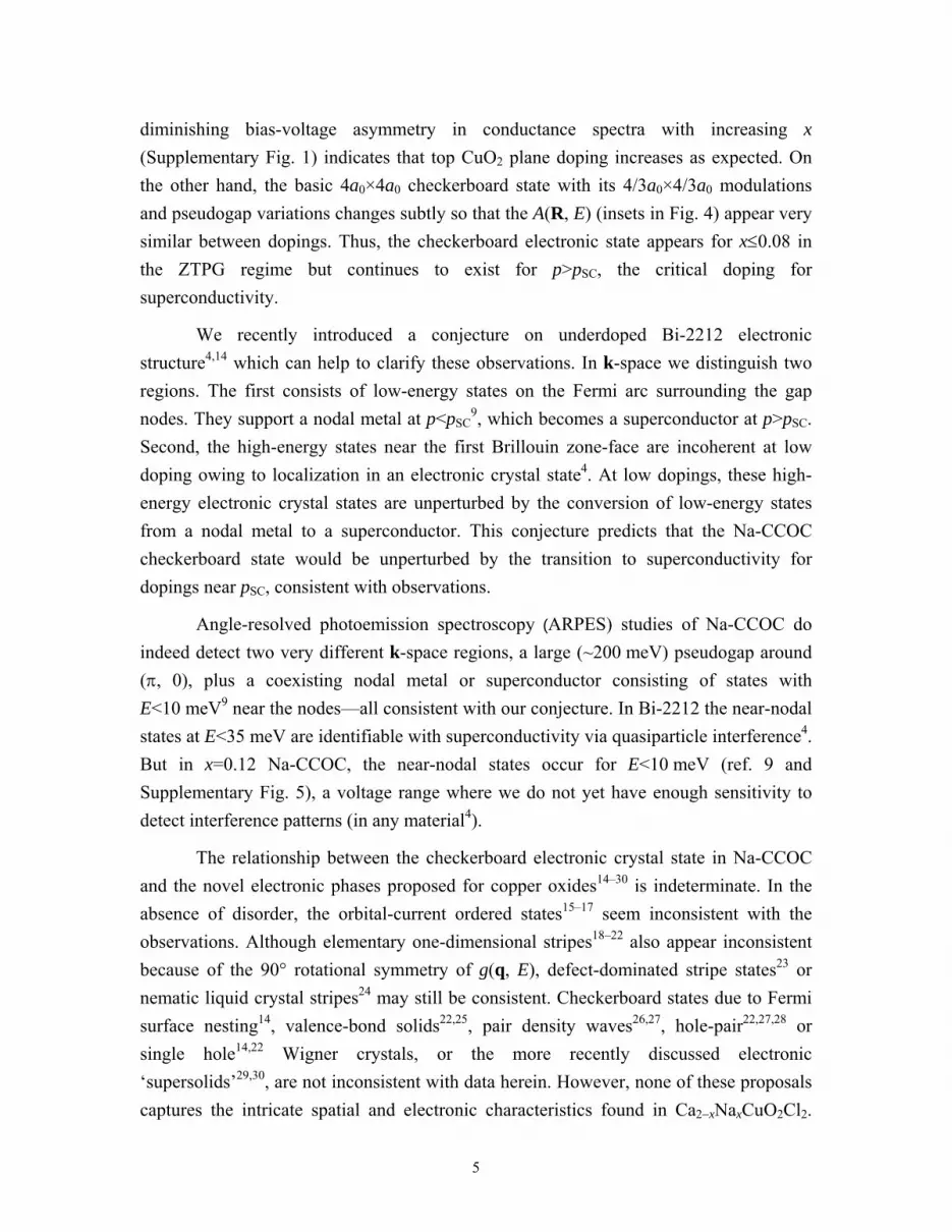
In Fig. 2a–c we show g(r, E) measured in the same field of view as Fig. 1d at energies 8, 24 and 48 meV. These and all other subgap g(r, E) are quite similar. The periodicities of modulations in g(r, E) are examined via their Fourier transforms g(q, E), as shown in Fig. 2d–f. These g(q, E) do not break symmetry under 90° rotations, an observation also noted at |E|<100 meV for all dopings. They also reveal three primary

4
sets of q-vectors contributing to the subgap g(q, E): q=(±1, 0); (0, ±1)2π/a0 from the lattice, q=(±1/4, 0); (0, ±1/4)2π/a0 from the commensurate 4a0×4a0 modulation, and an unanticipated q=(±3/4, 0); (0, ±3/4)2π/a0 modulation, which is also intense. Plots of Fourier intensity along the two orthogonal lines (2π, 0) and (0, 2π) in Fig. 2g–i show these effects directly. Significantly, these sets of q-vectors do not disperse with increasing energy and can also be detected as modulations in topographic images (Supplementary Fig. 2). All these observations are consistent with a crystalline electronic state.
To investigate spatial characteristics, we analyse autocorrelation images A(R, E)=⟨g(r, E) g(r+R, E)⟩. For example, A(R, E=24 meV) is shown in Fig. 3a. It clearly exhibits a basic 4a0×4a0 spatial modulation with a correlation length of ~10a0. For brevity, we refer to the 4a0×4a0 unit cell as a ‘tile’. Similar A(R, E) are found for all |E|<100 meV. The A(R, E) analysis also reveals that the internal electronic structure of representative 4a0×4a0 ‘tiles’ consists of 3×3 intense incommensurate conductance maxima, whose spectral weight is related to the strong q=(±3/4,0); (0, ±3/4)2π/a0 peaks in g(q, E).
The electronic structure within a representative 4a0×4a0 ‘tile’ is examined directly in Fig. 3b, which shows g(r, E=24 meV) measured within the blue box in Fig. 1e. Comparison between Fig. 3b and the simultaneously acquired topography Fig. 3c shows that the lowest conductance coincides with the perimeter atoms of a 4a0×4a0 ‘tile’, but that the local conductance maxima are not associated with atomic locations inside the tile (except for the central atom). Figure 3d shows the topographic signal (black) and simultaneously measured conductance (red) along a line through the tile centre.
The energetic changes occurring within a representative ‘tile’ are even more complex. In Fig. 3e, we show averages of spectra selected from representative regions of low conductance in Fig. 3b (white dots in Fig. 3c) and high conductance (red dots in Fig. 3c—see also Supplementary Fig. 3). From this we see that the pseudogap magnitude varies on the atomic scale by a factor of up to three. High pseudogap regions have low subgap conductance but also support a strong resonance at Ω=150 meV (arrow in Fig. 3e).
Next we consider the doping dependence of these phenomena. Bulk electronic transport studies at low temperatures show Ca2−xNaxCuO2Cl2 to be insulating at x=0.06, marginally conducting at x=0.08, and superconducting for x≥0.10 (Supplementary Fig. 4). The doping dependence of our subgap g(r, E) is summarized by Fig. 4. The
5
diminishing bias-voltage asymmetry in conductance spectra with increasing x (Supplementary Fig. 1) indicates that top CuO2 plane doping increases as expected. On the other hand, the basic 4a0×4a0 checkerboard state with its 4/3a0×4/3a0 modulations and pseudogap variations changes subtly so that the A(R, E) (insets in Fig. 4) appear very similar between dopings. Thus, the checkerboard electronic state appears for x≤0.08 in the ZTPG regime but continues to exist for p>pSC, the critical doping for superconductivity.
We recently introduced a conjecture on underdoped Bi-2212 electronic structure4,14 which can help to clarify these observations. In k-space we distinguish two regions. The first consists of low-energy states on the Fermi arc surrounding the gap nodes. They support a nodal metal at p<pSC
9, which becomes a superconductor at p>pSC. Second, the high-energy states near the first Brillouin zone-face are incoherent at low doping owing to localization in an electronic crystal state4. At low dopings, these high-energy electronic crystal states are unperturbed by the conversion of low-energy states from a nodal metal to a superconductor. This conjecture predicts that the Na-CCOC checkerboard state would be unperturbed by the transition to superconductivity for dopings near pSC, consistent with observations.
Angle-resolved photoemission spectroscopy (ARPES) studies of Na-CCOC do indeed detect two very different k-space regions, a large (~200 meV) pseudogap around (π, 0), plus a coexisting nodal metal or superconductor consisting of states with E<10 meV9 near the nodes—all consistent with our conjecture. In Bi-2212 the near-nodal states at E<35 meV are identifiable with superconductivity via quasiparticle interference4. But in x=0.12 Na-CCOC, the near-nodal states occur for E<10 meV (ref. 9 and Supplementary Fig. 5), a voltage range where we do not yet have enough sensitivity to detect interference patterns (in any material4).
The relationship between the checkerboard electronic crystal state in Na-CCOC and the novel electronic phases proposed for copper oxides14–30 is indeterminate. In the absence of disorder, the orbital-current ordered states15–17 seem inconsistent with the observations. Although elementary one-dimensional stripes18–22 also appear inconsistent because of the 90° rotational symmetry of g(q, E), defect-dominated stripe states23 or nematic liquid crystal stripes24 may still be consistent. Checkerboard states due to Fermi surface nesting14, valence-bond solids22,25, pair density waves26,27, hole-pair22,27,28 or single hole14,22 Wigner crystals, or the more recently discussed electronic ‘supersolids’29,30, are not inconsistent with data herein. However, none of these proposals captures the intricate spatial and electronic characteristics found in Ca2−xNaxCuO2Cl2.

6
Detailed theory of atomic-scale spectroscopic signatures for the various phases will be required to discriminate between them.
Independently of its microscopic identity, the Na-CCOC checkerboard state is significant because it exemplifies a (no longer hidden) electronic order associated with the copper-oxide pseudogap, and this order is not a translationally invariant liquid of electronic excitations but rather some form of electronic crystal.
Received 24 February; accepted 13 July 2004; doi:10.1038/nature02861.
1. Timusk, T. & Statt, B. The pseudogap in high-temperature superconductors: an experimental survey. Rep. Prog. Phys. 62, 61–122 (1999).
2. Hoffman, J. E. et al. A four unit cell periodic pattern of quasi-particle states surrounding vortex cores in Bi2Sr2CaCu2O8+δ. Science 295, 466–469 (2002).
3. Vershinin, M. et al. Local ordering in the pseudogap state of the high-Tc superconductor Bi2Sr2CaCu2O8+δ. Science 303, 1995–1998 (2004).
4. McElroy, K. et al. Destruction of antinodal state coherence via ‘checkerboard’ charge ordering in strongly underdoped superconducting Bi2Sr2CaCu2O8+δ. Preprint at <http://arXiv.org/cond-mat/0406491> (2004).
5. Howald, C., Fournier, P. & Kapitulnik, A. Inherent inhomogeneities in tunneling spectra of Bi2Sr2CaCu2O8-x crystals in the superconducting state. Phys. Rev. B 64, 100504 (2001).
6. Cren, T., Roditchev, D., Sacks, W. & Klein, J. Nanometer scale mapping of the density of states in an inhomogeneous superconductor. Europhys. Lett. 54, 84–90 (2001).
7. McElroy, K. et al. Relating atomic-scale electronic phenomena to wave-like quasiparticle states in superconducting Bi2Sr2CaCu2O8+δ. Nature 422, 592–596 (2003).
8. Ronning, F. et al. Photoemission evidence for a remnant Fermi surface and a d-wave-like dispersion in insulating Ca2CuO2Cl2. Science 282, 2067–2072 (1998).
9. Ronning, F. et al. Evolution of a metal to insulator transition in Ca2-xNaxCuO2Cl2 as seen by angle-resolved photoemission. Phys. Rev. B 67, 165101 (2003).

7
10. Hiroi, Z., Kobayashi, N. & Takano, M. Probable hole-doped superconductivity without apical oxygens in (Ca, Na)2CuO2Cl2. Nature 371, 139–141 (1994).
11. Kohsaka, Y. et al. Growth of Na-doped Ca2CuO2Cl2 single crystals under high pressures of several GPa. J. Am. Chem. Soc. 124, 12275–12278 (2002).
12. Kohsaka, Y. et al. Imaging nano-scale electronic inhomogeneity in lightly doped Mott insulator Ca2-xNaxCuO2Cl2. Phys. Rev. Lett. 93, 097004 (2004).
13. Wei, J. Y. T. et al. Quasiparticle tunneling spectra of the high-Tc mercury cuprates: Implications of the d-wave two-dimensional van Hove scenario. Phys. Rev. B 57, 3650–3662 (1998).
14. Fu, H. C., Davis, J. C. & Lee, D.-H. On the charge ordering observed by recent STM experiments. Preprint at <http://arXiv.org/cond-mat/0403001> (2004).
15. Varma, C. M. Non-Fermi-liquid states and pairing instability of a general model of copper oxide metals. Phys. Rev. B 55, 14554–14580 (1997).
16. Chakravarty, S., Laughlin, R. B., Morr, D. K. & Nayak, C. Hidden order in the cuprates. Phys. Rev. B 63, 094503 (2001).
17. Lee, P. A. Pseudogap and competing states in underdoped cuprates. Preprint at <http://arXiv.org/cond-mat/0307508> (2003).
18. Zaanen, J. & Gunnarsson, O. Charged magnetic domain lines and the magnetism of high-Tc oxides. Phys. Rev. B 40, 7391–7394 (1989).
19. Machida, K. Magnetism in La2CuO4 based compounds. Physica C 158, 192–196 (1989).
20. White, S. R. & Scalapino, D. J. Phase separation and stripe formation in the two-dimensional t-J model: A comparison of numerical results. Phys. Rev. B 61, 6320–6326 (2000).
21. Emery, V. J., Kivelson, S. A. & Tranquada, J. M. Stripe phases in high-temperature superconductors. Proc. Natl Acad. Sci. USA 96, 8814–8817 (1999).
22. Sachdev, S. Quantum criticality: Competing ground states in low dimensions. Science 288, 475–480 (2000).
23. Bosch, M., van Saarloos, W. & Zaanen, J. Shifting Bragg peaks of cuprate stripes as possible indications for fractionally charged kinks. Phys. Rev. B 63, 092501 (2001).

8
24. Kivelson, S. A., Fradkin, E. & Emery, V. J. Electronic liquid-crystal phases of a doped Mott insulator. Nature 393, 550–553 (1998).
25. Vojta, M. Superconducting charge-ordered states in cuprates. Phys. Rev. B 66, 104505 (2002).
26. Podolsky, D., Demler, E., Damle, K. & Halperin, B. I. Translational symmetry breaking in the superconducting state of the cuprates: Analysis of the quasiparticle density of states. Phys. Rev. B 67, 094514 (2003).
27. Chen, H.-D., Vafek, O., Yazdani, A. & Zhang, S.-C. Pair density wave in the pseudogap state of high temperature superconductors. Preprint at <http://arXiv.org/cond-mat/0402323> (2004).
28. Chen, H.-D., Hu, J.-P., Capponi, S., Arrigoni, E. & Zhang, S.-C. Antiferromagnetism and hole pair checkerboard in the vortex state of high Tc superconductors. Phys. Rev. Lett. 89, 137004 (2002).
29. Tešanović, Z. Charge modulation, spin response, and dual Hofstadter butterfly in high-Tc cuprates. Preprint at <http://arXiv.org/cond-mat/0405235> (2004).
30. Anderson, P. W. A suggested 4×4 structure in underdoped cuprate superconductors: a Wigner supersolid. Preprint at ⟨http://arXiv.org/cond-mat/0406038⟩ (2004).
Supplementary Information accompanies the paper on www.nature.com/nature.
Acknowledgements We acknowledge and thank P. Coleman, E. Demler, M. Franz, J. E. Hoffman, P. A.
Lee, K. Machida, K. McElroy, D. Pines, S. Sachdev, T. Senthil, T. Timusk, M. Vojta and J. Zaanen for
discussions and communications. This work was supported by the ONR, NSF, MEXT, JST and NEDO.
C.L. acknowledges support from a NSERC Postdoctoral Fellowship and Y.K. from a JPSJ Research
Fellowship for Young Scientists.
Competing interests statement The authors declare that they have no competing financial interests.
Correspondence and requests for materials should be addressed to J.C.D. ([email protected]) or
T.H. ([email protected]).
Figure 1 Atomic-scale explorations of electronic states in Ca2−xNaxCuO2Cl2. a, A schematic phase diagram of hole-doped copper-oxides showing the Mott insulator, high-Tc superconductor (HTSC) and metallic phases along with the ‘pseudogap’ regime and the ZTPG line. b, Crystal structure of Ca2−xNaxCuO2Cl2. Red, orange, blue and green spheres represent Ca(Na), Cu, O and Cl atoms, respectively. Conducting CuO2 planes are sandwiched by insulating CaCl layers. c, A characteristic spatially averaged tunnelling

9
conductance spectrum of x=0.12 Na-CCOC. The large particle–hole asymmetry in conductance at high energies can be associated with the light doping of a Mott insulator (see text). At low energies a skewed V-shaped gap exists. At energies below ~10 meV, changes occur in the spectra of superconducting samples (see Supplementary Fig. 5). The spectrum measured on equivalently underdoped Bi-2212 is shown in blue. d, High-resolution STM topograph of the cleaved CaCl plane of a crystal with x=0.10. The perfect square lattice, without discernible bulk or surface crystal reconstructions, is seen. The image was taken at a junction resistance of 4 GΩ and sample bias voltage Vs=+200 mV. e, The conductance map g(r, E) at E=+24 meV in the field of view of d. It reveals strong modulations with a 4a0×4a0 commensurate periodicity plus equally intense modulations at 4a0/3×4a0/3 and strong modulations at a0×a0. All data in this paper are acquired near T=100 mK in a dilution refrigerator-based scanning tunnelling microscope.
Figure 2 Energy dependence of the modulation wavevectors in the electronic crystal state. a–c, Images of differential conductance g(r, E) at E=+8, +24 and +48 meV in the same field of view as Fig. 1d; junction resistance was set to 2 GΩ at Vs=+200 mV. Such ‘checkerboard’ patterns are observed at all energies |E|<100 meV with strong correlations between the patterns at each energy. The dark low-conductance one-dimensional streaks are always registered to the atomic rows. The modulations are intense, using up to 90% peak-to-peak of the mean conductance at each energy. d–f, The calculated g(q, E) are Fourier transforms of the g(r, E) in a–c. Regions near the centre of each g(q, E) reflect the nanoscale electronic disorder. The modulations in g(q, E) contain three different q-vectors: q=(±1,0); (0, ±1)2π/a0, q=(±1/4,0); (0, ±1/4)2π/a0, and q=(±3/4,0); (0, ±3/4)2π/a0. Fourier transforms of these g(r, E) functions do not break 90° rotational symmetry, within the systematic uncertainty of the measurement as determined by the degree to which the atomic modulations q=(±1,0); (0, ±1)2π/a0 break this symmetry. All three dominant q-vectors do not disperse with energy. g–i, The magnitude of the Fourier transform is plotted along the (2π,0) (black filled circles) and (0, 2π) (red open circles) directions for each of these same g(r, E) and g(q, E) as in a–c and d–f.
Figure 3 Electronic structure imaging within a representative 4a0×4a0 ‘tile’. a, Autocorrelation image of typical |E|<100 meV LDOS maps showing the 4a0×4a0 structure inside a dark perimeter, which is exactly at the locations of the 16 atoms at the common perimeter between adjacent 4a0×4a0 regions. b, A representative tile of the 4a0×4a0 state is seen directly. The tile exhibits a very low conductance at the perimeter and high LDOS conductance pattern with nine incommensurate maxima inside. The average spatial electronic structure in a is remarkably consistent with electronic structure

10
of this (and other) tiles, but this should not be overemphasized because there is also a great deal of variability. Junction resistance for measurement was 2 GΩ at Vs=+400 mV. c, The simultaneously acquired topographic image showing the locations of what are believed to be the Cl atoms (light) above each Cu atom in the CuO2 plane. d, The topographic signal (black) and simultaneously measured conductance (red) along the line shown in c through the tile centre. e, Spectra show V-shaped pseudogaps regardless of the positions. The most remarkable difference between dark (low conductance) and bright (high conductance) spots in b appears in the positive bias voltage. At dark spots, a strong peak is observed at Ω≈+150 meV. On average the high pseudogap (most insulating) regions exhibit a strong resonance at Ω≈+150 meV so that the g(r, E=150 meV) is anticorrelated with the g(r, E) below 100 meV.
Figure 4 Doping dependence of electronic structure images. The g(r, E) patterns seen at three different dopings (x=0.08, 0.10, 0.12) are highly characteristic of lightly doped Na-CCOC. Although the high-energy spectra are changing (Supplementary Fig. 1), the subgap spatial characteristics are almost the same in the non-superconducting and superconducting phases in the energy range 10 meV<|E|<100 meV. The autocorrelation functions seen as insets appear very similar except for a slight increase in correlation length with increasing doping. The white scale bar in the inset corresponds to 2 nm.

Fig. 1
b
d e
CuO2
CuO2
CuO2
CaCl
CaCl
CaCl
CaCl
a c
0.06
0.53 nS
2 nm
0.0
1.5 Å
T*
Tc
T
p~0.1ZTPG p~0.2
HTSCpSC
Mot
t ins
ulat
or
Pseu
doga
p
Met
allic
-400 -200 0 200 4000.0
1.0
2.0
3.0
Sample bias (mV)N
a 0.1
2CC
OC
con
duct
ance
(nS)
0.0
0.5
UD
65K Bi2212 conductance (nS)
0.14
0.95 nS
0.06
0.53 nS
0.02
0.49 nS
Conductance Map Fourier transforms of map Line cuts of Fourier transforms
2 nm
8 mV
24 mV
48 mV
0
1
2
3
4
0
2
4
a g
h
i
b
c
0.0 0.5 1.0 1.50
2
4
6
q (2p/a0)
d1
14
34
e
f
114
34
Fig. 2

a b c
d e
-400 -200 0 200 4000
1
2
3
4
5C
ondu
ctan
ce (n
S)
Bias (mV)
Avg of white dots Avg of red dots
-4 -2 0 2 4 6
0.0
0.2
0.4
0.6
Distance (ao)
Topo
grap
hy (Å
)
0.00
0.10
0.20
0.30
0.40
+30 mV C
onductance Map (nS)
1 nm
0.0 1.0 Å
2 nm
+30 mV
0.05 0.57 nS
1 nm
Fig. 3

0.12
0.89 nS
ax=0.08
0.06
0.53 nS
bx=0.10
0.12
0.63 nS
c
2 nm
x=0.12
Fig. 4


