Embed Size (px)
Citation preview
Delft University of Technology
A High-Linearity and Low-EMI Multilevel Class-D Amplifier
Zhang, Huajun; Karmakar, Shoubhik; Breems, Lucien J.; Sandifort, Quino; Berkhout, Marco; Makinwa, KofiA.A.; Fan, QinwenDOI10.1109/JSSC.2020.3043815Publication date2020Document VersionFinal published versionPublished inIEEE Journal of Solid-State Circuits
Citation (APA)Zhang, H., Karmakar, S., Breems, L. J., Sandifort, Q., Berkhout, M., Makinwa, K. A. A., & Fan, Q. (2020). AHigh-Linearity and Low-EMI Multilevel Class-D Amplifier. IEEE Journal of Solid-State Circuits, 56(4), 1176-1185. [9305947]. https://doi.org/10.1109/JSSC.2020.3043815
Important noteTo cite this publication, please use the final published version (if applicable).Please check the document version above.
CopyrightOther than for strictly personal use, it is not permitted to download, forward or distribute the text or part of it, without the consentof the author(s) and/or copyright holder(s), unless the work is under an open content license such as Creative Commons.
Takedown policyPlease contact us and provide details if you believe this document breaches copyrights.We will remove access to the work immediately and investigate your claim.
This work is downloaded from Delft University of Technology.For technical reasons the number of authors shown on this cover page is limited to a maximum of 10.

Green Open Access added to TU Delft Institutional Repository
'You share, we take care!' - Taverne project
https://www.openaccess.nl/en/you-share-we-take-care
Otherwise as indicated in the copyright section: the publisher is the copyright holder of this work and the author uses the Dutch legislation to make this work public.
1176 IEEE JOURNAL OF SOLID-STATE CIRCUITS, VOL. 56, NO. 4, APRIL 2021
A High-Linearity and Low-EMI MultilevelClass-D Amplifier
Huajun Zhang , Graduate Student Member, IEEE, Shoubhik Karmakar , Graduate Student Member, IEEE,
Lucien J. Breems , Fellow, IEEE, Quino Sandifort, Marco Berkhout, Member, IEEE,Kofi A. A. Makinwa , Fellow, IEEE, and Qinwen Fan, Senior Member, IEEE
Abstract— This article presents a Class-D audio amplifier forautomotive applications. Low electromagnetic interference (EMI)and, hence, smaller LC filter size are obtained by employing afully differential multilevel output stage switching at 4.2 MHz.A modulation scheme with minimal switching activity at zeroinput reduces idle power, which is further assisted by agate-charge reuse scheme. It also achieves high linearity dueto the high loop gain realized by a third-order feedback loopwith a bandwidth of 800 kHz. The prototype, fabricated in a180-nm high-voltage BCD process, achieves a minimum THD+Nof −107.8 dB/−102 dB and a peak efficiency of 91%/87%with 8- and 4-� loads, respectively, while drawing 7-mA qui-escent current from a 14.4-V supply. The prototype meets theCISPR 25 Class 5 EMI standard with a 5.7-dB margin using anLC filter with a cutoff frequency of 580 kHz.
Index Terms— Class-D amplifiers, electromagnetic interference(EMI), idle power, multilevel, pulsewidth modulation (PWM).
I. INTRODUCTION
THE development of automotive infotainment systemshas driven the demand for high-performance and
high-efficiency audio amplifiers. Class-D amplifiers are wellsuited for this application because their high power efficiencysignificantly simplifies their cooling requirements, therebyreducing system cost and size [1]–[4]. However, Class-Damplifiers generate electromagnetic interference (EMI), whichoriginates from the high-frequency switching activities in theoutput stage, as shown in Fig. 1(a). This is then radiated bythe long cable harness connecting the power supply, audioamplifiers, and speakers and, thus, can be problematic inautomotive applications, which must comply with a strict EMIstandard (e.g., CISPR 25 Class 5 [5]). To meet the stringentautomotive EMI requirement, fully differential switching ispreferred since it produces much less common-mode (CM)
Manuscript received August 16, 2020; revised November 3, 2020; acceptedNovember 30, 2020. Date of publication December 23, 2020; date of currentversion March 26, 2021. This article was approved by Associate EditorBrian Ginsburg. (Corresponding author: Qinwen Fan.)
Huajun Zhang, Shoubhik Karmakar, Kofi A. A. Makinwa, and Qinwen Fanare with the Faculty of Electrical Engineering, Mathematics and ComputerScience (EEMCS), Department of Microelectronics, Delft University ofTechnology, 2628 CD Delft, The Netherlands (e-mail: [email protected]).
Lucien J. Breems is with NXP Semiconductors, 5656 AE Eindhoven,The Netherlands.
Quino Sandifort is with NXP Semiconductors, 6534 AE Nijmegen,The Netherlands.
Marco Berkhout is with Goodix Technologies, 6537 TL Nijmegen,The Netherlands.
Color versions of one or more figures in this article are available athttps://doi.org/10.1109/JSSC.2020.3043815.
Digital Object Identifier 10.1109/JSSC.2020.3043815
EMI, which can be a significant contributor to radiated emis-sion [6], [7]. The residual EMI must then be suppressed by anLC filter at the output of the Class-D amplifier. Unfortunately,this significantly increases system cost and bulk.
Multiphase [6] and multilevel output stages [8]–[17]have been proposed to mitigate EMI. In multiphase outputstages [see Fig. 1(b)] [6], several output stages drive separateinductors and switch at different moments. Therefore, the totalhigh-frequency ripple current delivered to the load is reduced,which also reduces EMI. However, this increases the numberof inductors required, as well as the idle power dissipationcaused by the ripple currents circulating in the variousoutput stages. As the number of audio channels increases,the total system cost and idle power dissipation increaseproportionally. Multilevel output stages [see Fig. 1(c)] reduceEMI by reducing the switching step size. In [8]–[13], thisis achieved by using multiple supply voltages, which oftenincreases system cost. Alternatively, this can be done by using(relatively low-cost) external flying capacitors to generate anintermediate output level equal to a fraction (usually 1/2) ofthe supply [14], [15]. However, the extra control circuitry isrequired to fix the voltage across these capacitors at half of thesupply, thus increasing design complexity. In [16], an extraoutput level is created by simply shorting the load, but itrequires zero dead time for proper operation, resulting in acomplicated gate-driving configuration. In [17], independentcontrol of the back-to-back transistors shorting the load isproposed, which obviates zero dead time. However, in bothcases, extra circuitry and, thus, idle power are required torobustly define the output CM.
Another way to meet the EMI challenge is by tailoringit to the requirements of the CISPR 25 EMI mask. Class-Damplifiers employing fixed-frequency pulsewidth modulation(PWM) [1] or a hybrid of PWM and �� modulation [2] caneffectively reduce the LC filter size by switching at frequenciesabove 1.8 MHz where the EMI requirements are relaxed.However, this results in increased switching loss and, hence,higher idle power. On the other hand, Class-D amplifiersemploying �� modulation [also known as pulse densitymodulation (PDM)] [13], [17]–[19] can reduce EMI peaks byspreading the switching energy, which is useful in consumerapplications. However, even with sampling frequencies ofseveral MHz, their out-of-band quantization noise still fallswithin the AM band, thus requiring a bulky LC filter to satisfyCISPR 25.
0018-9200 © 2020 IEEE. Personal use is permitted, but republication/redistribution requires IEEE permission.See https://www.ieee.org/publications/rights/index.html for more information.
Authorized licensed use limited to: TU Delft Library. Downloaded on March 29,2021 at 09:46:53 UTC from IEEE Xplore. Restrictions apply.
ZHANG et al.: HIGH-LINEARITY AND LOW-EMI MULTILEVEL CLASS-D AMPLIFIER 1177
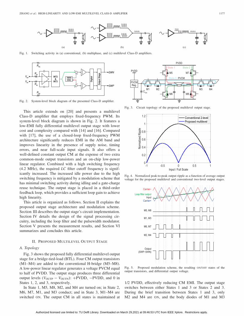
Fig. 1. Switching activity in (a) conventional, (b) multiphase, and (c) multilevel Class-D amplifiers.
Fig. 2. System-level block diagram of the presented Class-D amplifier.
This article extends on [20] and presents a multilevelClass-D amplifier that employs fixed-frequency PWM. Itssystem-level block diagram is shown in Fig. 2. It features alow-EMI fully differential multilevel output stage with lowercost and complexity compared with [14] and [16]. Comparedwith [17], the use of a closed-loop fixed-frequency PWMarchitecture significantly reduces EMI in the AM band andimproves linearity in the presence of supply noise, timingerrors, and near full-scale input signals. It also offers awell-defined constant output CM at the expense of two extracommon-mode output transistors and an on-chip low-powerlinear regulator. Combined with a high switching frequency(4.2 MHz), the required LC filter cutoff frequency is signif-icantly increased. The increased idle power due to the highswitching frequency is mitigated by a modulation scheme thathas minimal switching activity during idling and a gate-chargereuse technique. The output stage is placed in a third-orderfeedback loop, which provides a sufficient loop gain to achievehigh linearity.
This article is organized as follows. Section II explains theproposed output stage architecture and modulation scheme.Section III describes the output stage’s circuit implementation.Section IV details the design of the signal processing cir-cuitry, including the loop filter and the pulsewidth modulator.Section V presents the measurement results, and Section VIsummarizes and concludes this article.
II. PROPOSED MULTILEVEL OUTPUT STAGE
A. Topology
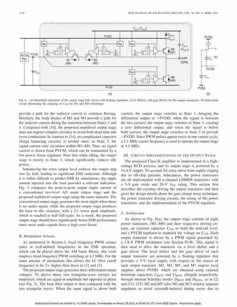
Fig. 3 shows the proposed fully differential multilevel outputstage for a bridge-tied-load (BTL). Four CM output transistors(M1–M4) are added to the conventional H-bridge (M5–M8).A low-power linear regulator generates a voltage PVCM equalto half of PVDD. The output stage produces three differentialoutput levels (VOUTP − VOUTN): +PVDD, −PVDD, and 0 inStates 1, 2, and 3, respectively.
In State 1, M5, M8, M2, and M4 are turned on; in State 2,M6, M7, M1, and M3 conduct; and in State 3, M1–M4 areswitched ON. The output CM in all states is maintained at
Fig. 3. Circuit topology of the proposed multilevel output stage.
Fig. 4. Normalized peak-to-peak output ripple as a function of average outputvoltage for the proposed multilevel and conventional two-level output stages.
Fig. 5. Proposed modulation scheme, the resulting ON/OFF states of theoutput transistors, and differential output voltage.
1/2 PVDD, effectively reducing CM EMI. The output stageswitches between either States 1 and 3 or States 2 and 3.During the brief transition between States 1 and 3, onlyM2 and M4 are ON, and the body diodes of M1 and M3
Authorized licensed use limited to: TU Delft Library. Downloaded on March 29,2021 at 09:46:53 UTC from IEEE Xplore. Restrictions apply.
1178 IEEE JOURNAL OF SOLID-STATE CIRCUITS, VOL. 56, NO. 4, APRIL 2021
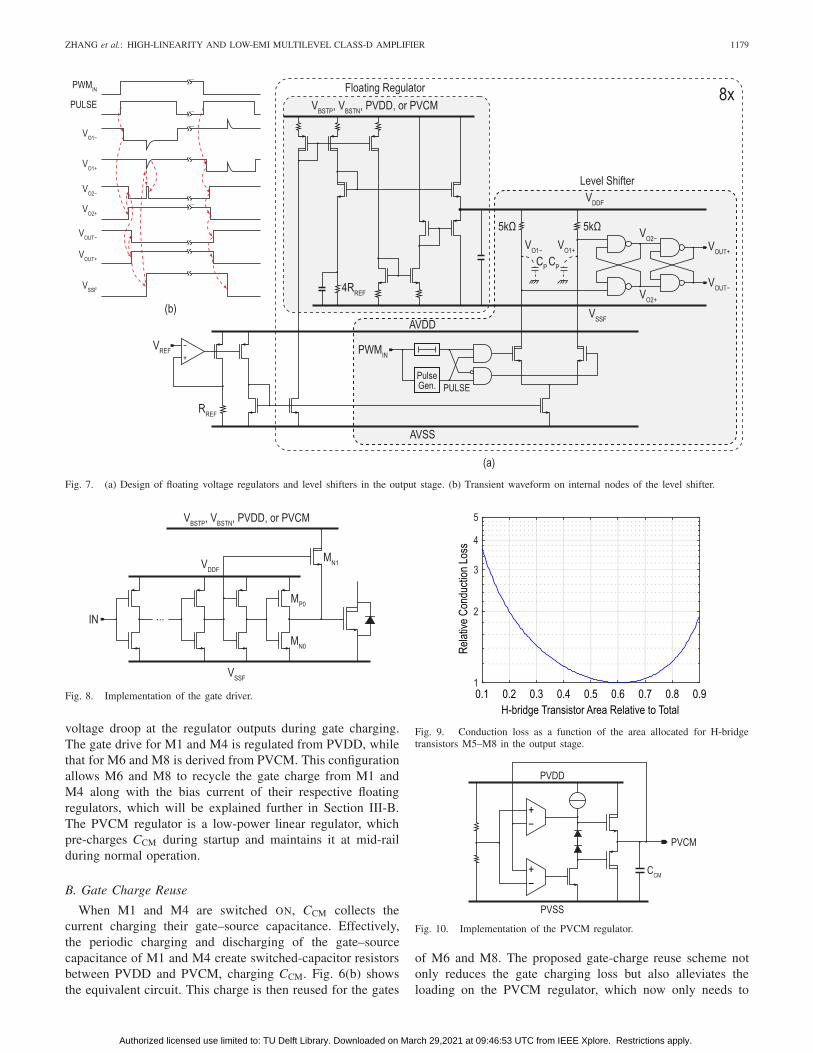
Fig. 6. (a) Simplified schematic of the output stage half circuit with floating regulators, level shifters, and gate drivers for the output transistors. (b) Equivalentcircuit illustrating the charging of CCM by M1 and M4 switchings.
provide a path for the inductor current to continue flowing.Similarly, the body diodes of M2 and M4 provide a path forthe inductor current during the transition between States 2 and3. Compared with [16], the proposed multilevel output stagedoes not require complex circuitry to avoid both dead time andcross-conduction. In contrast to [14], no complicated capacitorcharge balancing circuitry is needed since, in State 3, thesignal current only circulates within M1–M4. Thus, no signalcurrent is drawn from PVCM, which can be maintained by alow-power linear regulator. Note that while idling, the outputstage is mostly in State 3, which significantly reduces idlepower.
Introducing the extra output level reduces the output stepsize by half, leading to significant EMI reduction. Althoughit is rather difficult to predict EMI by simulations, the ripplecurrent injected into the load provides a relevant indication.Fig. 4 compares the peak-to-peak output ripple current ofa conventional two-level AD mode output stage and theproposed multilevel output stage using the same inductor. Theconventional output stage generates the most ripple when thereis no audio signal, while the proposed output stage producesthe least in this situation, with a 2× lower peak amplitude,which is reached at half full-scale. As a result, the proposedoutput stage should have significantly better EMI performancesince most audio signals have a high crest factor.
B. Modulation Scheme
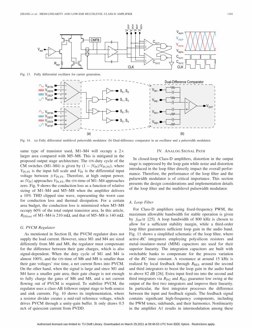
As mentioned in Section I, fixed frequency PWM createstones at well-defined frequencies in the EMI spectrum,which can be placed above the AM band. Hence, this workemploys fixed-frequency PWM switching at 4.2 MHz. For thesame amount of attenuation, this allows the LC filter cutofffrequency to be 2× higher than those in [1] and [2].
The proposed output stage generates three differential outputvoltages. To derive them, two triangular-wave carriers areemployed, which are equal in amplitude but opposite in phase(see Fig. 5). The loop filter output is then compared with thetwo triangular waves. When the input signal is above both
carriers, the output stage switches to State 1, bringing thedifferential output to +PVDD; when the signal is betweenthe two carriers, the output stage switches to State 3, creatinga zero differential output; and when the signal is belowboth carriers, the output stage switches to State 2 to provide−PVDD. Since PWM pulses appear twice in one carrier cycle,a 2.1-MHz carrier frequency is used to operate the output stageat 4.2 MHz.
III. CIRCUIT IMPLEMENTATION OF THE OUTPUT STAGE
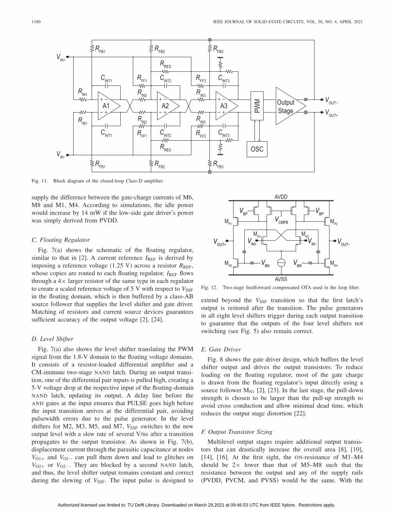
The proposed Class-D amplifier is implemented in a high-voltage BCD process, and its output stage is powered by a14.4-V supply. To account for extra stress from supply ringingdue to off-chip parasitic inductances, the power transistorsare all implemented with n-channel LDMOS transistors witha 5-V gate oxide and 20-V VDS rating. This section firstdescribes the circuitry driving the output transistors and thengives the design details about the gate-charge reuse technique,the power transistor driving circuits, the sizing of the powertransistors, and the implementation of the PVCM regulator.
A. Architecture
As shown in Fig. 6(a), the output stage consists of eightpower transistors (M1–M8) and their respective driving cir-cuits, an external capacitor CCM to hold the mid-rail level,and a PVCM regulator to maintain the voltage on CCM. Eachoutput transistor is driven by a PWM signal generated bya 1.8-V PWM modulator (see Section IV-B). This signal isthen used to drive the transistor via a level shifter and agate driver. The level shifter and the gate driver of eachoutput transistor are powered by a floating regulator thatprovides a 5-V local supply with respect to the source ofeach output transistor. M2, M3, M5, and M7 require localsupplies above PVDD, which are obtained using externalbootstrap capacitors CBSTP and CBSTN charged, respectively,through internal Schottky diodes DBSTP and DBSTN, as in [2]and [21]–[23]. M2 and M5 (also M3 and M7) employ separateregulators to avoid crosstalk-induced timing errors due to
Authorized licensed use limited to: TU Delft Library. Downloaded on March 29,2021 at 09:46:53 UTC from IEEE Xplore. Restrictions apply.
ZHANG et al.: HIGH-LINEARITY AND LOW-EMI MULTILEVEL CLASS-D AMPLIFIER 1179
Fig. 7. (a) Design of floating voltage regulators and level shifters in the output stage. (b) Transient waveform on internal nodes of the level shifter.
Fig. 8. Implementation of the gate driver.
voltage droop at the regulator outputs during gate charging.The gate drive for M1 and M4 is regulated from PVDD, whilethat for M6 and M8 is derived from PVCM. This configurationallows M6 and M8 to recycle the gate charge from M1 andM4 along with the bias current of their respective floatingregulators, which will be explained further in Section III-B.The PVCM regulator is a low-power linear regulator, whichpre-charges CCM during startup and maintains it at mid-railduring normal operation.
B. Gate Charge Reuse
When M1 and M4 are switched ON, CCM collects thecurrent charging their gate–source capacitance. Effectively,the periodic charging and discharging of the gate–sourcecapacitance of M1 and M4 create switched-capacitor resistorsbetween PVDD and PVCM, charging CCM. Fig. 6(b) showsthe equivalent circuit. This charge is then reused for the gates
Fig. 9. Conduction loss as a function of the area allocated for H-bridgetransistors M5–M8 in the output stage.
Fig. 10. Implementation of the PVCM regulator.
of M6 and M8. The proposed gate-charge reuse scheme notonly reduces the gate charging loss but also alleviates theloading on the PVCM regulator, which now only needs to
Authorized licensed use limited to: TU Delft Library. Downloaded on March 29,2021 at 09:46:53 UTC from IEEE Xplore. Restrictions apply.
1180 IEEE JOURNAL OF SOLID-STATE CIRCUITS, VOL. 56, NO. 4, APRIL 2021
Fig. 11. Block diagram of the closed-loop Class-D amplifier.
supply the difference between the gate-charge currents of M6,M8 and M1, M4. According to simulations, the idle powerwould increase by 14 mW if the low-side gate driver’s powerwas simply derived from PVDD.
C. Floating Regulator
Fig. 7(a) shows the schematic of the floating regulator,similar to that in [2]. A current reference IREF is derived byimposing a reference voltage (1.25 V) across a resistor RREF,whose copies are routed to each floating regulator. IREF flowsthrough a 4× larger resistor of the same type in each regulatorto create a scaled reference voltage of 5 V with respect to VSSF
in the floating domain, which is then buffered by a class-ABsource follower that supplies the level shifter and gate driver.Matching of resistors and current source devices guaranteessufficient accuracy of the output voltage [2], [24].
D. Level Shifter
Fig. 7(a) also shows the level shifter translating the PWMsignal from the 1.8-V domain to the floating voltage domains.It consists of a resistor-loaded differential amplifier and aCM-immune two-stage NAND latch. During an output transi-tion, one of the differential pair inputs is pulled high, creating a5-V voltage drop at the respective input of the floating-domainNAND latch, updating its output. A delay line before theAND gates at the input ensures that PULSE goes high beforethe input transition arrives at the differential pair, avoidingpulsewidth errors due to the pulse generator. In the levelshifters for M2, M3, M5, and M7, VSSF switches to the newoutput level with a slew rate of several V/ns after a transitionpropagates to the output transistor. As shown in Fig. 7(b),displacement current through the parasitic capacitance at nodesVO1+ and VO1− can pull them down and lead to glitches onVO2+ or VO2−. They are blocked by a second NAND latch,and thus, the level shifter output remains constant and correctduring the slewing of VSSF. The input pulse is designed to
Fig. 12. Two-stage feedforward compensated OTA used in the loop filter.
extend beyond the VSSF transition so that the first latch’soutput is restored after the transition. The pulse generatorsin all eight level shifters trigger during each output transitionto guarantee that the outputs of the four level shifters notswitching (see Fig. 5) also remain correct.
E. Gate Driver
Fig. 8 shows the gate driver design, which buffers the levelshifter output and drives the output transistors. To reduceloading on the floating regulator, most of the gate chargeis drawn from the floating regulator’s input directly using asource follower MN1 [2], [23]. In the last stage, the pull-downstrength is chosen to be larger than the pull-up strength toavoid cross conduction and allow minimal dead time, whichreduces the output stage distortion [22].
F. Output Transistor Sizing
Multilevel output stages require additional output transis-tors that can drastically increase the overall area [8], [10],[14], [16]. At the first sight, the ON-resistance of M1–M4should be 2× lower than that of M5–M8 such that theresistance between the output and any of the supply rails(PVDD, PVCM, and PVSS) would be the same. With the
Authorized licensed use limited to: TU Delft Library. Downloaded on March 29,2021 at 09:46:53 UTC from IEEE Xplore. Restrictions apply.
ZHANG et al.: HIGH-LINEARITY AND LOW-EMI MULTILEVEL CLASS-D AMPLIFIER 1181
Fig. 13. Fully differential oscillator for carrier generation.
Fig. 14. (a) Fully differential multilevel pulsewidth modulator. (b) Dual-difference comparator in an oscillator and a pulsewidth modulator.
same type of transistor used, M1–M4 will occupy a 2×larger area compared with M5–M8. This is mitigated in theproposed output stage architecture. The ON-duty cycle of theCM switches (M1–M4) is given by (1 − |VIN|/VIN,FS), whereVIN,FS is the input full scale and VIN is the differential inputvoltage between ±VIN,FS. Therefore, at high output power,as |VIN| approaches VIN,FS, the ON-time of M1–M4 approacheszero. Fig. 9 shows the conduction loss as a function of relativesizing of M1–M4 and M5–M8 when the amplifier deliversa 10% THD clipped sine wave, representing the worst casefor conduction loss and thermal dissipation. For a certainarea budget, the conduction loss is minimized when M5–M8occupy 60% of the total output transistor area. In this article,RDS(on) of M1–M4 is 210 m�, and that of M5–M8 is 140 m�.
G. PVCM Regulator
As mentioned in Section II, the PVCM regulator does notsupply the load current. However, since M1 and M4 are sizeddifferently from M6 and M8, the regulator must compensatefor the difference between their gate charges, which is alsosignal-dependent. When the duty cycle of M1 and M4 isalmost 100%, and the ON-time of M6 and M8 is smaller thantheir gate voltages’ rise time, a net current flows into PVCM.On the other hand, when the signal is large and since M1 andM4 have a smaller gate area, their gate charge is not enoughto fully charge the gates of M6 and M8, and a net currentflowing out of PVCM is required. To stabilize PVCM, theregulator uses a class-AB follower output stage to both sourceand sink currents. Fig. 10 shows its implementation, wherea resistor divider creates a mid-rail reference voltage, whichdrives PVCM through a unity-gain buffer. It only draws 0.5mA of quiescent current from PVDD.
IV. ANALOG SIGNAL PATH
In closed-loop Class-D amplifiers, distortion in the outputstage is suppressed by the loop gain while noise and distortionintroduced in the loop filter directly impact the overall perfor-mance. Therefore, the performance of the loop filter and thepulsewidth modulator is of critical importance. This sectionpresents the design considerations and implementation detailsof the loop filter and the multilevel pulsewidth modulator.
A. Loop Filter
For Class-D amplifiers using fixed-frequency PWM, themaximum allowable bandwidth for stable operation is givenby fSW/π [25]. A loop bandwidth of 800 kHz is chosen toallow for a sufficient stability margin, while a third-orderloop filter guarantees sufficient loop gain in the audio band.Fig. 11 shows a simplified schematic of the loop filter, whereactive-RC integrators employing polysilicon resistors andmetal–insulator–metal (MIM) capacitors are used for theirsuperior linearity. The integration capacitors are built withswitchable banks to compensate for the process variationof the RC time constant. A resonance at around 15 kHz isrealized by local feedback through RRES around the secondand third integrators to boost the loop gain in the audio bandto above 82 dB [26]. Extra input feed-ins into the second andthird integrators via RIN2 and RIN3 guarantee low swing at theoutput of the first two integrators and improve their linearity.In particular, the first integrator processes the differencebetween the input and feedback signals. The feedback signalcontains significant high-frequency components, includingthe PWM tones, sidebands, and their harmonics. Nonlinearityin the amplifier A1 results in intermodulation among these
Authorized licensed use limited to: TU Delft Library. Downloaded on March 29,2021 at 09:46:53 UTC from IEEE Xplore. Restrictions apply.
1182 IEEE JOURNAL OF SOLID-STATE CIRCUITS, VOL. 56, NO. 4, APRIL 2021
Fig. 15. Die micrograph.
Fig. 16. Measured output voltage of the Class-D amplifier before the LCfilter (SWP and SWN) and after the LC filter (OUTP).
Fig. 17. Measured audio band spectrum when the prototype drives a 1-Wsine wave into an 8-� load.
components, which is directly added to the input and leadsto in-band distortion.
To mitigate this effect, a two-stage feedforward-compensated OTA instead of a conventional two-stageMiller compensated OTA is employed, as shown in Fig. 12.Feedforward compensation is implemented by ac-couplingthe inputs to MN3 and MN4 in the second stage [2]. Thisallows for 14 dB of extra gain at the switching frequencyto suppress the intermodulation distortion compared with aconventional Miller-compensated OTA without increasing thepower consumption.
Fig. 18. Measured THD+N of the prototype across output power.
Fig. 19. Measured power efficiency at different output powers.
B. Pulsewidth Modulator
As described in Section II, multilevel PWM is realizedby comparing the loop filter output with two equal butopposite triangle waves. They are generated by the fullydifferential oscillator shown in Fig. 13, built around a fullydifferential OTA. When the absolute value of its differentialoutput exceeds (VREFP − VREFN), one of the comparatorstoggles, reversing the polarity of integration using a chopper.The resulting triangle carrier frequency is proportional to1/(RREFCINT). CINT is made of trimmable banks to compensatefor the process variation of the RC time constant so that theoscillator operates near 2.1 MHz. The same trim codes arethen applied to the loop filter to center its transfer function.In the prototype, VREF is provided externally to fine-tune theoscillator to 2.1 MHz. The loop filter output (VINT3P − VINT3N)is compared with the two triangle waves (VOSCP − VOSCN)and (VOSCN − VOSCP) using two dual-difference comparators,as shown in Fig. 14, where the two differential inputs arecombined using an all-pass passive network. The fully dif-ferential operation offers robustness against CM noise andmismatch (e.g., substrate noise) between the carrier and inputcompared with single-ended implementations [8], [27], [28].Here, as in other time-interleaved systems, the mismatchbetween two comparators and imbalances in the differentialtriangle wave results in a residual spur at the carrier frequency
Authorized licensed use limited to: TU Delft Library. Downloaded on March 29,2021 at 09:46:53 UTC from IEEE Xplore. Restrictions apply.
ZHANG et al.: HIGH-LINEARITY AND LOW-EMI MULTILEVEL CLASS-D AMPLIFIER 1183
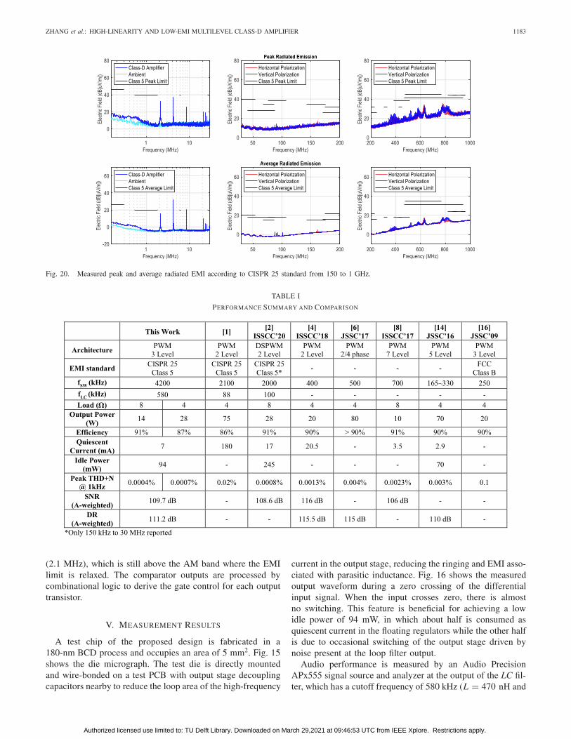
Fig. 20. Measured peak and average radiated EMI according to CISPR 25 standard from 150 to 1 GHz.
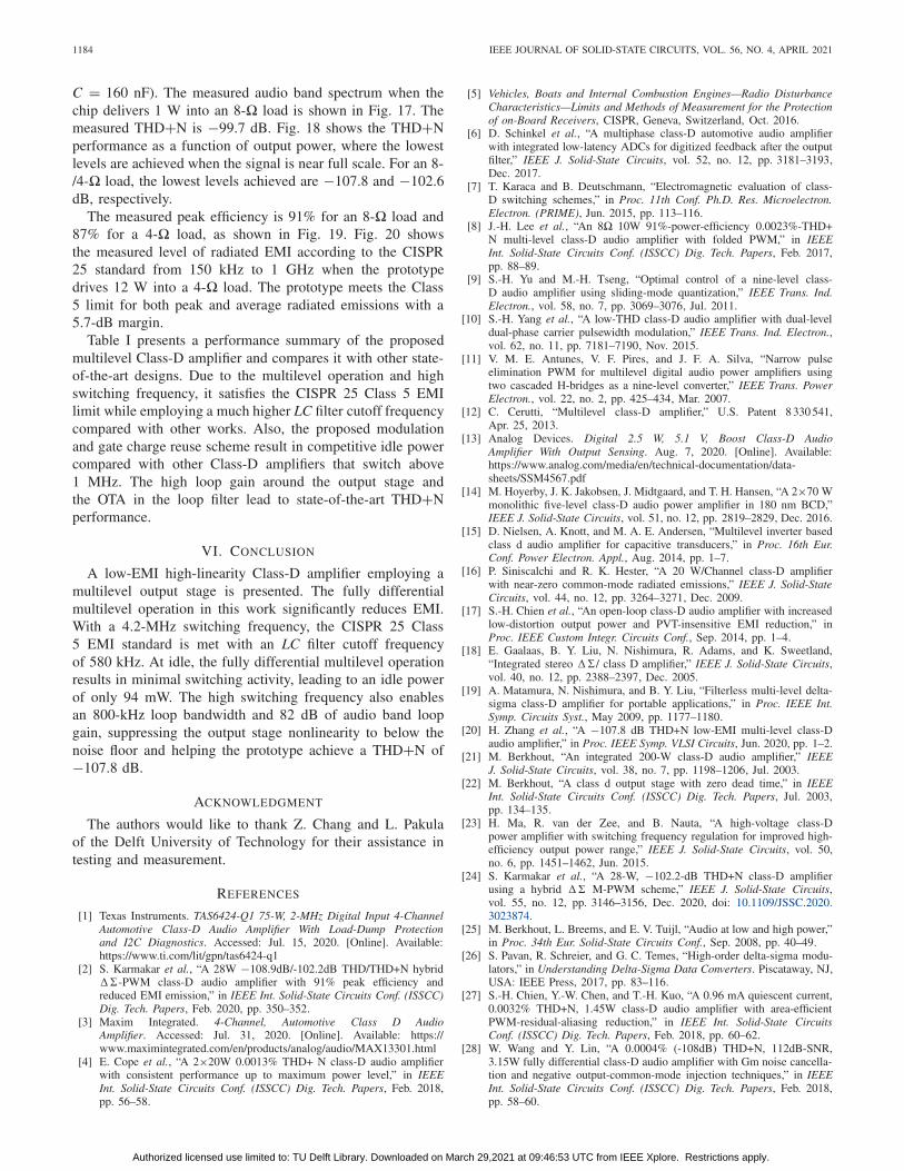
TABLE I
PERFORMANCE SUMMARY AND COMPARISON
(2.1 MHz), which is still above the AM band where the EMIlimit is relaxed. The comparator outputs are processed bycombinational logic to derive the gate control for each outputtransistor.
V. MEASUREMENT RESULTS
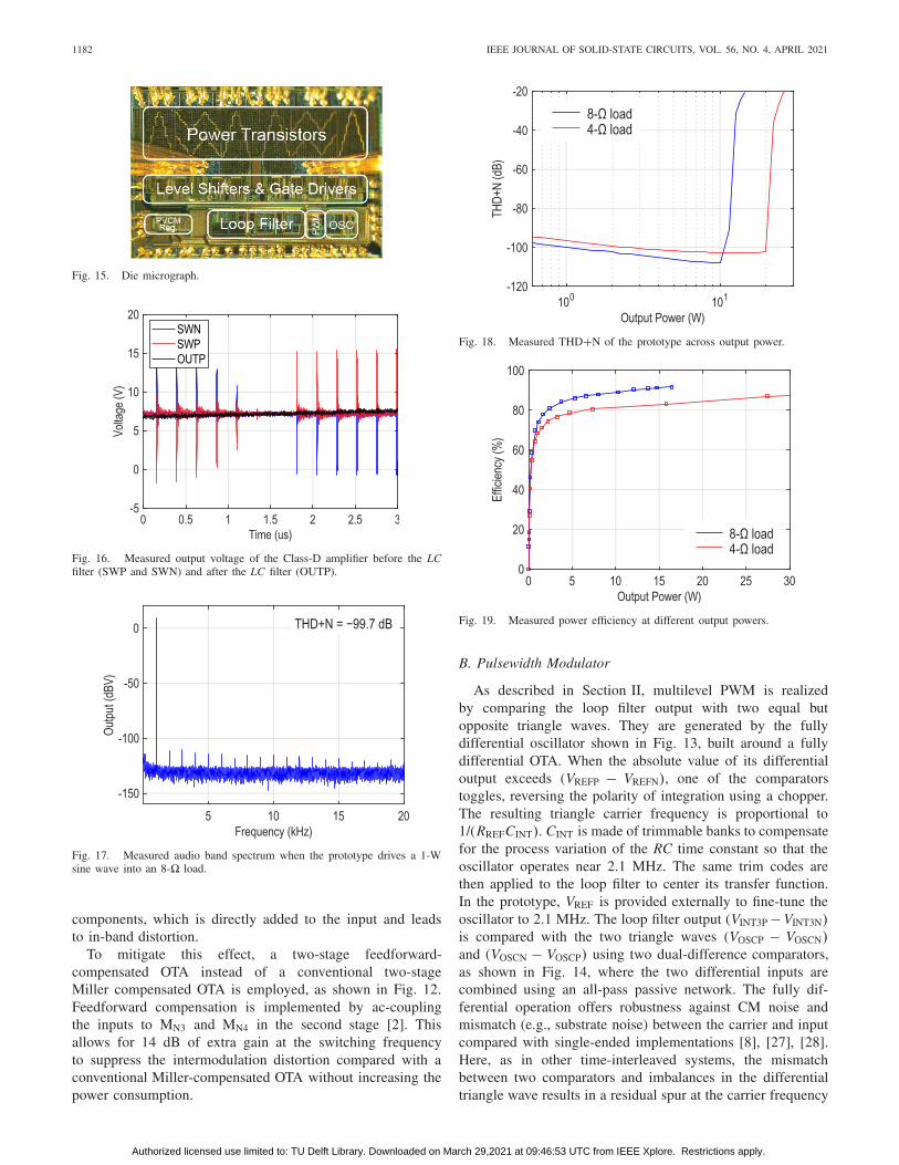
A test chip of the proposed design is fabricated in a180-nm BCD process and occupies an area of 5 mm2. Fig. 15shows the die micrograph. The test die is directly mountedand wire-bonded on a test PCB with output stage decouplingcapacitors nearby to reduce the loop area of the high-frequency
current in the output stage, reducing the ringing and EMI asso-ciated with parasitic inductance. Fig. 16 shows the measuredoutput waveform during a zero crossing of the differentialinput signal. When the input crosses zero, there is almostno switching. This feature is beneficial for achieving a lowidle power of 94 mW, in which about half is consumed asquiescent current in the floating regulators while the other halfis due to occasional switching of the output stage driven bynoise present at the loop filter output.
Audio performance is measured by an Audio PrecisionAPx555 signal source and analyzer at the output of the LC fil-ter, which has a cutoff frequency of 580 kHz (L = 470 nH and
Authorized licensed use limited to: TU Delft Library. Downloaded on March 29,2021 at 09:46:53 UTC from IEEE Xplore. Restrictions apply.
1184 IEEE JOURNAL OF SOLID-STATE CIRCUITS, VOL. 56, NO. 4, APRIL 2021
C = 160 nF). The measured audio band spectrum when thechip delivers 1 W into an 8-� load is shown in Fig. 17. Themeasured THD+N is −99.7 dB. Fig. 18 shows the THD+Nperformance as a function of output power, where the lowestlevels are achieved when the signal is near full scale. For an 8-/4-� load, the lowest levels achieved are −107.8 and −102.6dB, respectively.
The measured peak efficiency is 91% for an 8-� load and87% for a 4-� load, as shown in Fig. 19. Fig. 20 showsthe measured level of radiated EMI according to the CISPR25 standard from 150 kHz to 1 GHz when the prototypedrives 12 W into a 4-� load. The prototype meets the Class5 limit for both peak and average radiated emissions with a5.7-dB margin.
Table I presents a performance summary of the proposedmultilevel Class-D amplifier and compares it with other state-of-the-art designs. Due to the multilevel operation and highswitching frequency, it satisfies the CISPR 25 Class 5 EMIlimit while employing a much higher LC filter cutoff frequencycompared with other works. Also, the proposed modulationand gate charge reuse scheme result in competitive idle powercompared with other Class-D amplifiers that switch above1 MHz. The high loop gain around the output stage andthe OTA in the loop filter lead to state-of-the-art THD+Nperformance.
VI. CONCLUSION
A low-EMI high-linearity Class-D amplifier employing amultilevel output stage is presented. The fully differentialmultilevel operation in this work significantly reduces EMI.With a 4.2-MHz switching frequency, the CISPR 25 Class5 EMI standard is met with an LC filter cutoff frequencyof 580 kHz. At idle, the fully differential multilevel operationresults in minimal switching activity, leading to an idle powerof only 94 mW. The high switching frequency also enablesan 800-kHz loop bandwidth and 82 dB of audio band loopgain, suppressing the output stage nonlinearity to below thenoise floor and helping the prototype achieve a THD+N of−107.8 dB.
ACKNOWLEDGMENT
The authors would like to thank Z. Chang and L. Pakulaof the Delft University of Technology for their assistance intesting and measurement.
REFERENCES
[1] Texas Instruments. TAS6424-Q1 75-W, 2-MHz Digital Input 4-ChannelAutomotive Class-D Audio Amplifier With Load-Dump Protectionand I2C Diagnostics. Accessed: Jul. 15, 2020. [Online]. Available:https://www.ti.com/lit/gpn/tas6424-q1
[2] S. Karmakar et al., “A 28W −108.9dB/-102.2dB THD/THD+N hybrid��-PWM class-D audio amplifier with 91% peak efficiency andreduced EMI emission,” in IEEE Int. Solid-State Circuits Conf. (ISSCC)Dig. Tech. Papers, Feb. 2020, pp. 350–352.
[3] Maxim Integrated. 4-Channel, Automotive Class D AudioAmplifier. Accessed: Jul. 31, 2020. [Online]. Available: https://www.maximintegrated.com/en/products/analog/audio/MAX13301.html
[4] E. Cope et al., “A 2×20W 0.0013% THD+ N class-D audio amplifierwith consistent performance up to maximum power level,” in IEEEInt. Solid-State Circuits Conf. (ISSCC) Dig. Tech. Papers, Feb. 2018,pp. 56–58.
[5] Vehicles, Boats and Internal Combustion Engines—Radio DisturbanceCharacteristics—Limits and Methods of Measurement for the Protectionof on-Board Receivers, CISPR, Geneva, Switzerland, Oct. 2016.
[6] D. Schinkel et al., “A multiphase class-D automotive audio amplifierwith integrated low-latency ADCs for digitized feedback after the outputfilter,” IEEE J. Solid-State Circuits, vol. 52, no. 12, pp. 3181–3193,Dec. 2017.
[7] T. Karaca and B. Deutschmann, “Electromagnetic evaluation of class-D switching schemes,” in Proc. 11th Conf. Ph.D. Res. Microelectron.Electron. (PRIME), Jun. 2015, pp. 113–116.
[8] J.-H. Lee et al., “An 8� 10W 91%-power-efficiency 0.0023%-THD+N multi-level class-D audio amplifier with folded PWM,” in IEEEInt. Solid-State Circuits Conf. (ISSCC) Dig. Tech. Papers, Feb. 2017,pp. 88–89.
[9] S.-H. Yu and M.-H. Tseng, “Optimal control of a nine-level class-D audio amplifier using sliding-mode quantization,” IEEE Trans. Ind.Electron., vol. 58, no. 7, pp. 3069–3076, Jul. 2011.
[10] S.-H. Yang et al., “A low-THD class-D audio amplifier with dual-leveldual-phase carrier pulsewidth modulation,” IEEE Trans. Ind. Electron.,vol. 62, no. 11, pp. 7181–7190, Nov. 2015.
[11] V. M. E. Antunes, V. F. Pires, and J. F. A. Silva, “Narrow pulseelimination PWM for multilevel digital audio power amplifiers usingtwo cascaded H-bridges as a nine-level converter,” IEEE Trans. PowerElectron., vol. 22, no. 2, pp. 425–434, Mar. 2007.
[12] C. Cerutti, “Multilevel class-D amplifier,” U.S. Patent 8 330 541,Apr. 25, 2013.
[13] Analog Devices. Digital 2.5 W, 5.1 V, Boost Class-D AudioAmplifier With Output Sensing. Aug. 7, 2020. [Online]. Available:https://www.analog.com/media/en/technical-documentation/data-sheets/SSM4567.pdf
[14] M. Hoyerby, J. K. Jakobsen, J. Midtgaard, and T. H. Hansen, “A 2×70 Wmonolithic five-level class-D audio power amplifier in 180 nm BCD,”IEEE J. Solid-State Circuits, vol. 51, no. 12, pp. 2819–2829, Dec. 2016.
[15] D. Nielsen, A. Knott, and M. A. E. Andersen, “Multilevel inverter basedclass d audio amplifier for capacitive transducers,” in Proc. 16th Eur.Conf. Power Electron. Appl., Aug. 2014, pp. 1–7.
[16] P. Siniscalchi and R. K. Hester, “A 20 W/Channel class-D amplifierwith near-zero common-mode radiated emissions,” IEEE J. Solid-StateCircuits, vol. 44, no. 12, pp. 3264–3271, Dec. 2009.
[17] S.-H. Chien et al., “An open-loop class-D audio amplifier with increasedlow-distortion output power and PVT-insensitive EMI reduction,” inProc. IEEE Custom Integr. Circuits Conf., Sep. 2014, pp. 1–4.
[18] E. Gaalaas, B. Y. Liu, N. Nishimura, R. Adams, and K. Sweetland,“Integrated stereo ��/ class D amplifier,” IEEE J. Solid-State Circuits,vol. 40, no. 12, pp. 2388–2397, Dec. 2005.
[19] A. Matamura, N. Nishimura, and B. Y. Liu, “Filterless multi-level delta-sigma class-D amplifier for portable applications,” in Proc. IEEE Int.Symp. Circuits Syst., May 2009, pp. 1177–1180.
[20] H. Zhang et al., “A −107.8 dB THD+N low-EMI multi-level class-Daudio amplifier,” in Proc. IEEE Symp. VLSI Circuits, Jun. 2020, pp. 1–2.
[21] M. Berkhout, “An integrated 200-W class-D audio amplifier,” IEEEJ. Solid-State Circuits, vol. 38, no. 7, pp. 1198–1206, Jul. 2003.
[22] M. Berkhout, “A class d output stage with zero dead time,” in IEEEInt. Solid-State Circuits Conf. (ISSCC) Dig. Tech. Papers, Jul. 2003,pp. 134–135.
[23] H. Ma, R. van der Zee, and B. Nauta, “A high-voltage class-Dpower amplifier with switching frequency regulation for improved high-efficiency output power range,” IEEE J. Solid-State Circuits, vol. 50,no. 6, pp. 1451–1462, Jun. 2015.
[24] S. Karmakar et al., “A 28-W, −102.2-dB THD+N class-D amplifierusing a hybrid �� M-PWM scheme,” IEEE J. Solid-State Circuits,vol. 55, no. 12, pp. 3146–3156, Dec. 2020, doi: 10.1109/JSSC.2020.3023874.
[25] M. Berkhout, L. Breems, and E. V. Tuijl, “Audio at low and high power,”in Proc. 34th Eur. Solid-State Circuits Conf., Sep. 2008, pp. 40–49.
[26] S. Pavan, R. Schreier, and G. C. Temes, “High-order delta-sigma modu-lators,” in Understanding Delta-Sigma Data Converters. Piscataway, NJ,USA: IEEE Press, 2017, pp. 83–116.
[27] S.-H. Chien, Y.-W. Chen, and T.-H. Kuo, “A 0.96 mA quiescent current,0.0032% THD+N, 1.45W class-D audio amplifier with area-efficientPWM-residual-aliasing reduction,” in IEEE Int. Solid-State CircuitsConf. (ISSCC) Dig. Tech. Papers, Feb. 2018, pp. 60–62.
[28] W. Wang and Y. Lin, “A 0.0004% (-108dB) THD+N, 112dB-SNR,3.15W fully differential class-D audio amplifier with Gm noise cancella-tion and negative output-common-mode injection techniques,” in IEEEInt. Solid-State Circuits Conf. (ISSCC) Dig. Tech. Papers, Feb. 2018,pp. 58–60.
Authorized licensed use limited to: TU Delft Library. Downloaded on March 29,2021 at 09:46:53 UTC from IEEE Xplore. Restrictions apply.
ZHANG et al.: HIGH-LINEARITY AND LOW-EMI MULTILEVEL CLASS-D AMPLIFIER 1185
Huajun Zhang (Graduate Student Member, IEEE)received the B.E. degree in electrical and computerengineering from Shanghai Jiao Tong University,Shanghai, China, in 2015, and the B.S.E. and M.S.degrees in electrical engineering from the Universityof Michigan, Ann Arbor, MI, USA, in 2015 and2017, respectively. He is currently pursuing thePh.D. degree with the Delft University of Technol-ogy, Delft, The Netherlands.
In summer 2016, he was an Analog/Mixed SignalDesign Intern with Analog Devices, Inc., Wilming-
ton, MA, USA. From May 2017 to February 2019, he was a Mixed SignalDesign Engineer with Analog Devices, Inc., Norwood, MA, USA. He joinedthe Electronic Instrumentation Laboratory, Delft University of Technology,in March 2019. He holds one U.S. patent. His technical interests includeprecision analog circuits, class-D audio amplifiers, and ultralow-power dataconverters.
Mr. Zhang has served as a Reviewer for the IEEE TRANSACTIONS ON
CIRCUITS AND SYSTEMS I: REGULAR PAPERS and the IEEE SENSORS
JOURNAL.
Shoubhik Karmakar (Graduate Student Member,IEEE) received the B.E. degree in electrical andelectronics engineering from the Birla Institute ofTechnology and Science, Pilani, India, in 2012,and the M.Sc. degree from the Delft University ofTechnology, Delft, The Netherlands, in 2017, wherehe is currently pursuing the Ph.D. degree.
His current research interests include energy-efficient data converters and high-performanceclass-D amplifiers for audio applications.
Lucien J. Breems (Fellow, IEEE) received theM.Sc. degree (cum laude) and the Ph.D. degree inelectrical engineering from the Delft University ofTechnology, Delft, The Netherlands, in 1996 and2001, respectively.
From 2000 to 2006, he was with Philips Research,Nijmegen, The Netherlands. In 2007, he joined NXPSemiconductors, Eindhoven, The Netherlands. Since2011, he has been a part-time Professor with theTechnical University of Eindhoven, Eindhoven.
Dr. Breems has been a member of the TechnicalProgram Committees of the International Solid-State Circuits Conference(ISSCC), the European Solid-State Circuits Conference (ESSCIRC), theSymposium on VLSI Circuits, and the IEEE International Symposium onLow Power Electronics and Design (ISLPED). He received the ISSCC Janvan Vessem Outstanding European Paper Awards in 2001, 2011, and 2016, theRFIC Symposium Industry Best Paper Award in 2016, and the IEEE Journal ofSolid-State Circuits Best Paper Awards in 2011 and 2016. From 2009 to 2015,he served as an Associate Editor and, in 2020, as a Guest Editor for the IEEEJOURNAL OF SOLID-STATE CIRCUITS. He was a Guest Editor of the IEEETRANSACTIONS ON CIRCUITS AND SYSTEMS II from 2008 to 2009. He wasthe IEEE Distinguished Lecturer from 2012 to 2013.
Quino Sandifort received the B.Sc. degree in elec-trical and electronic engineering, with a special-ization in both analog and digital, from SaxionUniversity, Enschede, The Netherlands, in 1998.
From September 1998 to 2007, he was withPhilips Semiconductors, Nijmegen, The Nether-lands. He joined NXP Semiconductors, Nijmegen,in 2007, where he fulfilled several positions as theAnalog/Mixed-Signal IC Designer for automotiveapplications. Since 2008, he has been active as anAnalog/Mixed-Signal IC Architect covering topics
like audio, analog integration, interference, and EMC for automotive applica-tions.
Marco Berkhout (Member, IEEE) received theM.Sc. degree in electrical engineering and the Ph.D.degree from the University of Twente, Enschede,The Netherlands, in 1992 and 1996, respectively.
From 1996 to 2019, he was with Philips/NXPSemiconductors, Nijmegen, The Netherlands. He iscurrently a fellow with Goodix Technologies,Nijmegen. His main interests are class-D amplifiersand integrated power electronics.
Dr. Berkhout was a member of the TechnicalProgram Committees of the European Solid-State
Circuits Conference (ESSCIRC) from 2008 to 2018 and the InternationalSolid-State Circuits Conference (ISSCC) from 2013 to 2016, where he willalso be a member in 2021. He received the 2002 ESSCIRC Best Paper Awardand was a plenary invited speaker on audio at low and high powers at the2008 ESSCIRC.
Kofi A. A. Makinwa (Fellow, IEEE) received theB.Sc. and M.Sc. degrees from Obafemi AwolowoUniversity, Ife, Nigeria, in 1985 and 1988,respectively, the M.E.E. degree from the PhilipsInternational Institute, Eindhoven, The Netherlands,in 1989, and the Ph.D. degree from the Delft Univer-sity of Technology, Delft, The Netherlands, in 2004.
From 1989 to 1999, he was a Research Scientistwith Philips Research Laboratories, Eindhoven,where he worked on interactive displays and digitalrecording systems. In 1999, he joined the Delft
University of Technology, where he is currently an Antoni van LeeuwenhoekProfessor and the Head of the Microelectronics Department. This has resultedin 16 books and over 250 technical articles. He holds over 30 patents.His research interests include the design of mixed-signal circuits, sensorinterfaces, and smart sensors.
Dr. Makinwa is also a member of the Royal Netherlands Academy ofArts and Sciences and the Editorial Board of the PROCEEDINGS OF THE
IEEE. He was a co-recipient of 15 Best Paper Awards, including twofrom the IEEE JOURNAL OF SOLID-STATE CIRCUITS (JSSC) and threefrom the International Solid-State Circuits Conference (ISSCC). At the 60thanniversary of ISSCC, he was recognized as a Top-Ten Contributor. He isalso the Analog Subcommittee Chair of the ISSCC and a Co-Organizer forthe Advances in Analog Circuit Design (AACD) Workshop and the SensorInterfaces Meeting. He has been on the program committees of severalIEEE conferences. He has served the IEEE Solid-State Circuits Society asa Distinguished Lecturer and an elected member of its AdCom. He has alsoserved as a Guest Editor for the IEEE JSSC.
Qinwen Fan (Senior Member, IEEE) received theB.Sc. degree in electronic science and technologyfrom Nankai University, Tianjin, China, in 2006,and the M.Sc. degree (cum laude) and the Ph.D.degree in microelectronics from the Delft Universityof Technology, Delft, The Netherlands, in 2008 and2013, respectively.
From August 2007 to August 2008, she was anIntern with NXP Research Laboratories, Eindhoven,The Netherlands, where she designed a precisioninstrumentation amplifier for biomedical purposes.
From October 2012 to May 2015, she was with Maxim Integrated Products,Delft. From June 2015 to January 2017, she was with Mellanox, Delft.In 2017, she rejoined the Delft University of Technology, where she iscurrently an Assistant Professor with the Electronics and InstrumentationLaboratory. Her current research interests include precision analog, class Daudio amplifiers, dc–dc converters for energy harvesters, and current-sensingamplifiers.
Dr. Fan also serves as a TPC Member of the European Solid-State Cir-cuits Conference and a Reviewer for the IEEE JOURNAL OF SOLID-STATE
CIRCUITS.
Authorized licensed use limited to: TU Delft Library. Downloaded on March 29,2021 at 09:46:53 UTC from IEEE Xplore. Restrictions apply.


