Embed Size (px)
Citation preview
Contribution to conducted EMI reduction in multiconverter topology
J. Mon, D. González, J. Gago, J. Balcells, R. Fernández, I. Gil
Departament d’Enginyeria Electrònica. Universitat Politècnica de Catalunya. [email protected]
Abstract-This paper contributes to the conducted EMI
reduction generated by switched power converters operating in multiconverter arrangement. The EMI reduction is achieved by means of the combination of two techniques: interleaving and switching frequency modulation. The effectiveness of such methods in terms of EMI reduction is experimentally validated in a four channel parallel buck converter. The technique that provides the best attenuation results is identified. Finally, special attention has been paid to possible undesired side-effects produced by these techniques. For this reason the converter efficiency and output voltage ripple are evaluated.
I. INTRODUCTION
Since the switching frequency modulation was introduced in the past decade as a EMI reduction technique in switched power converters a lot of works have been published developing this idea [1-9]. At present, it is a well established technique and a worthy alternative to the traditional filtering methods such as the bulky EMI filters or snubber networks in terms of attenuation, cost and simplicity of application. It has been demonstrated in [5] that the side effects of such technique are negligible in front of the attenuation advantages that it provides. Although this technique has been mainly applied to Switching Mode Power Supplies (SMPS) with single converter topology it has been also used in electronic ballasts applications [7] and home cooking appliances [8].
However, the application of modulation techniques in distributed or modular power systems made up of several power converters has not been deeply studied yet.
On the other hand, in modular power systems with parallel topology, interleaving technique is commonly used to reduce EMI and output voltage ripple. In a few words, interleaving technique consists of introducing a given shift delay among the switching patterns of the converters, resulting in harmonics cancellation effect [10-14].
In this work, we deal with the simultaneous application of interleaving and modulation techniques to modular power supplies systems with parallel topology. The first goal of this paper is to evaluate the optimal combination of interleaving and switching frequency modulation in order to reach the best results in terms of EMI attenuation. The second goal is to identify undesired side-effects of such techniques on the converter performance. This paper focuses its attention in the experimental analysis of two particular techniques that have been presented in [15]. In the development of our research, several combinations of interleaving and modulation were tested. The two techniques validated here are those that provide the best attenuation performance. The experimental
validation has been performed on four buck converters connected in parallel.
The paper is organized as follows. First of all, in Section II some theoretical considerations regarding interleaving, switching frequency modulation and the combined application of both techniques are presented. The experimental arrangement is described in Section III. The experimental results that confirm the validity of this approach are shown in Section IV. In this Section two kinds of results are presented: EMI reduction spectrum and converter performance in terms of converter efficiency and output voltage ripple. Finally, the conclusions are summarized in Section V, where some future woks are also pointed out.
II. THEORETICAL BACKGROUND
There are several possibilities in order to reduce the conducted EMI in modular power systems with parallel topology. In this work four of them are analysed: interleaving, Switching Frequency Modulation (SFM), Constant Delay with switching Frequency Modulation (CDFM) and Variable Delay with switching Frequency Modulation (VDFM).
A. Interleaving
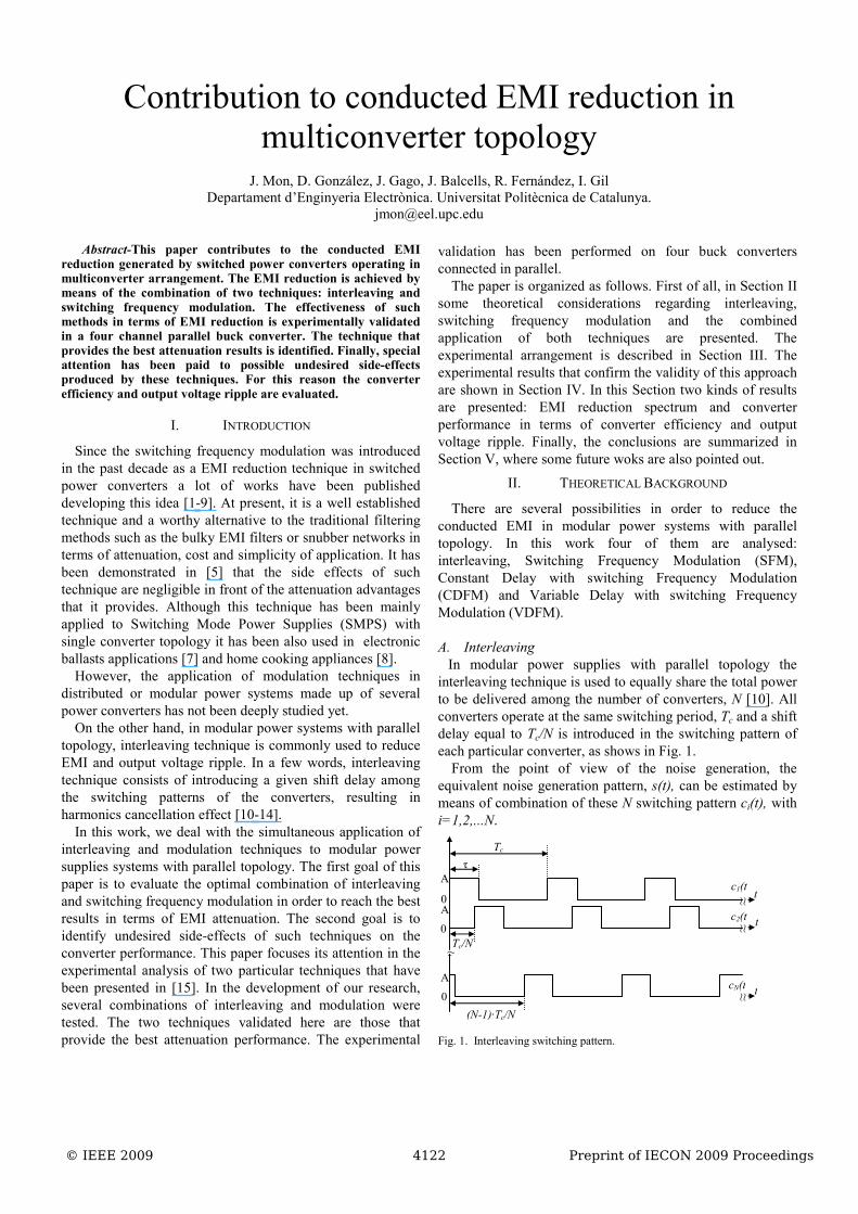
In modular power supplies with parallel topology the interleaving technique is used to equally share the total power to be delivered among the number of converters, N [10]. All converters operate at the same switching period, Tc and a shift delay equal to Tc/N is introduced in the switching pattern of each particular converter, as shows in Fig. 1.
From the point of view of the noise generation, the equivalent noise generation pattern, s(t), can be estimated by means of combination of these N switching pattern ci(t), with i=1,2,...N. Fig. 1. Interleaving switching pattern.
c1(t
Tc
Tc/N
A
0A
0
A
0
c2(t
cN(t
τ
≈≈
≈
t
t
t
(N-1)·Tc/N
≈
© IEEE 2009 4122 Preprint of IECON 2009 Proceedings
The time domain expressions of the switching pattern, ci(t), and the equivalent noise generation pattern, s(t), are given by (1), where subindex i corresponds to each of the N switching patterns and k notes the switching cycle.
( )⎪⎪⎪⎪
⎩
⎪⎪⎪⎪
⎨
⎧
<≤−
−
<≤
<
=
∑∞
= ⎟⎟⎠
⎞⎜⎜⎝
⎛⎟⎟⎠
⎞⎜⎜⎝
⎛−−−−−⎟⎟
⎠
⎞⎜⎜⎝
⎛−−−=
∑⎥⎥⎦
⎤
⎢⎢⎣
⎡∑ ⎟
⎟⎠
⎞⎜⎜⎝
⎛⎟⎟⎠
⎞⎜⎜⎝
⎛⎟⎟⎠
⎞⎜⎜⎝
⎛ −−−−⎟⎟⎠
⎞⎜⎜⎝
⎛ −+===
∞
=
cTN
cTNN
NcT
NcT
NcT
B
ki
NcT
ckTtuiNcT
ckTtuAtic
NT
NT
ktuNT
ktuBAtctsN
i k
ccci
τ
τ
τ
τ
τ
·1,1
...
·2,1
,0
0)1()1(·)(
·)()(1 0
(1)
The equivalent noise source pattern, s(t), generated by all
converters is equal to the generated by a single converter switching at a constant frequency of N·fc. The shift delay introduced in each switching pattern does not change the amplitude of interference harmonics, but it modifies the harmonic phases. This effect produces a suppression of harmonics which frequency is not multiple of N·fc [11,12]. In other words, the resulting spectrum consists of harmonics at frequencies multiple of N·fc. The relationship in frequency domain between Ci(w) and S(w) can be found in [13,14]. Therefore, the interleaving technique has shown itself to be a harmonic cancellation method.
B. Modulation
The modulation technique concept mainly consists of varying a certain parameter of the switching pattern, which normally is the switching frequency, around a central value according to a modulation law, Vm(t). If the switching frequency is the modulated parameter the result is that the harmonics energy is distributed in side-bands, resulting in a global attenuation of interference harmonics amplitude.
In case of using a periodic modulation profile, the distance between two consecutive side-bands harmonics is given by the frequency of modulation profile, fm [1].
fc ‐Δfc
Tm
Vm(t)fc +Δfc
t fc
Tm
t
Tk
τk
Fig. 2. Switching frequency modulation.
Figure 2 shows a switching pattern modulated according to a triangular profile, where fc is the central frequency, Δfc is the maximum frequency deviation, Tm is the period of modulation profile and Tk is the instantaneous switching period.
When a triangular modulation profile is used, the amplitude reduction, ΔdB, of each interference harmonics can be estimated by (2), where n is the harmonic order [9].
⎟⎟⎠
⎞⎜⎜⎝
⎛ Δ−=Δ
m
cdB f
fn··log10 10 (2)
For the shake of space, all the relations among modulation
parameters and Resolution Bandwidth (RBW) of measuring device are omitted. A thorough description of such relations can be found in [5].
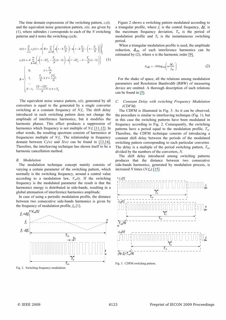
C. Constant Delay with switching Frequency Modulation
(CDFM). The CDFM is illustrated in Fig. 3. As it can be observed,
the procedure is similar to interleaving technique (Fig. 1), but in this case the switching patterns have been modulated in frequency according to Fig. 2. Consequently, the switching patterns have a period equal to the modulation profile, Tm. Therefore, the CDFM technique consists of introducing a constant shift delay between the periods of the modulated switching pattern corresponding to each particular converter. The delay is a multiple of the period switching pattern, Tm, divided by the numbers of the converters, N.
The shift delay introduced among switching patterns produces that the distance between two consecutive side-bands harmonics, generated by modulation process, is increased N times (N·fm) [15].
≈
≈
≈
≈
Fig. 3. CDFM switching pattern.
© IEEE 2009 4123 Preprint of IECON 2009 Proceedings
(a)
(b)
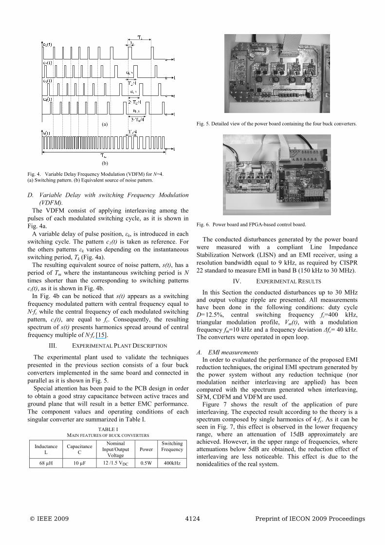
Fig. 4. Variable Delay Frequency Modulation (VDFM) for N=4. (a) Switching pattern. (b) Equivalent source of noise pattern.
D. Variable Delay with switching Frequency Modulation
(VDFM). The VDFM consist of applying interleaving among the
pulses of each modulated switching cycle, as it is shown in Fig. 4a.
A variable delay of pulse position, εk, is introduced in each switching cycle. The pattern c1(t) is taken as reference. For the others patterns εk varies depending on the instantaneous switching period, Tk (Fig. 4a).
The resulting equivalent source of noise pattern, s(t), has a period of Tm where the instantaneous switching period is N times shorter than the corresponding to switching patterns ci(t), as it is shown in Fig. 4b.
In Fig. 4b can be noticed that s(t) appears as a switching frequency modulated pattern with central frequency equal to N·fc while the central frequency of each modulated switching pattern, ci(t), are equal to fc. Consequently, the resulting spectrum of s(t) presents harmonics spread around of central frequency multiple of N·fc [15].
III. EXPERIMENTAL PLANT DESCRIPTION
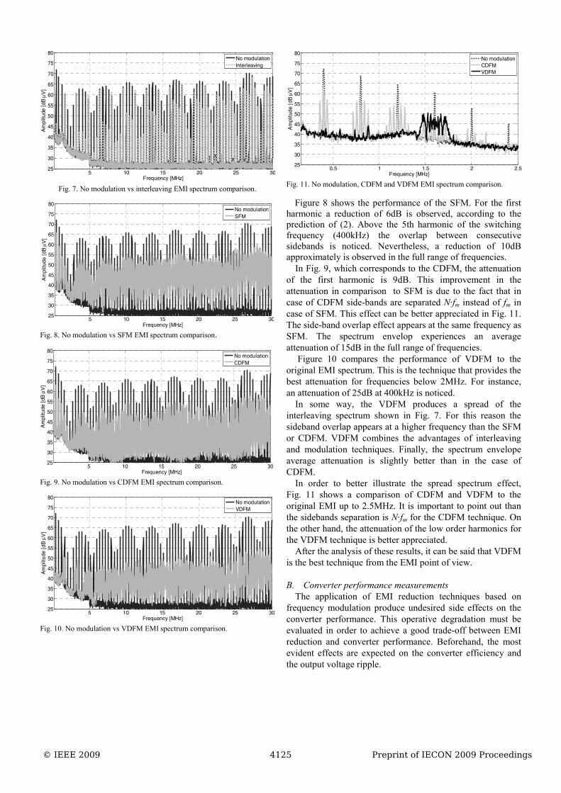
The experimental plant used to validate the techniques presented in the previous section consists of a four buck converters implemented in the same board and connected in parallel as it is shown in Fig. 5.
Special attention has been paid to the PCB design in order to obtain a good stray capacitance between active traces and ground plane that will result in a better EMC performance. The component values and operating conditions of each singular converter are summarized in Table I.
TABLE I MAIN FEATURES OF BUCK CONVERTERS
Inductance L
Capacitance C
Nominal Input/Output
Voltage Power
Switching Frequency
68 µH 10 µF 12 /1.5 VDC 0.5W 400kHz
Fig. 5. Detailed view of the power board containing the four buck converters.
Fig. 6. Power board and FPGA-based control board.
The conducted disturbances generated by the power board
were measured with a compliant Line Impedance Stabilization Network (LISN) and an EMI receiver, using a resolution bandwidth equal to 9 kHz, as required by CISPR 22 standard to measure EMI in band B (150 kHz to 30 MHz).
IV. EXPERIMENTAL RESULTS
In this Section the conducted disturbances up to 30 MHz and output voltage ripple are presented. All measurements have been done in the following conditions: duty cycle D=12.5%, central switching frequency fc=400 kHz, triangular modulation profile, Vm(t), with a modulation frequency fm=10 kHz and a frequency deviation Δfc= 40 kHz. The converters were operated in open loop.
A. EMI measurements
In order to evaluated the performance of the proposed EMI reduction techniques, the original EMI spectrum generated by the power system without any reduction technique (nor modulation neither interleaving are applied) has been compared with the spectrum generated when interleaving, SFM, CDFM and VDFM are used.
Figure 7 shows the result of the application of pure interleaving. The expected result according to the theory is a spectrum composed by single harmonics of 4·fc. As it can be seen in Fig. 7, this effect is observed in the lower frequency range, where an attenuation of 15dB approximately are achieved. However, in the upper range of frequencies, where attenuations below 5dB are obtained, the reduction effect of interleaving are less noticeable. This effect is due to the nonidealities of the real system.
© IEEE 2009 4124 Preprint of IECON 2009 Proceedings
5 10 15 20 25 3025
30
35
40
45
50
55
60
65
70
75
80
Frequency [MHz]
Am
plitu
de [
dBμV
]
No modulationInterleaving
Fig. 7. No modulation vs interleaving EMI spectrum comparison.
5 10 15 20 25 3025
30
35
40
45
50
55
60
65
70
75
80
Frequency [MHz]
Am
plitu
de [
dBμ V
]
No modulationSFM
Fig. 8. No modulation vs SFM EMI spectrum comparison.
5 10 15 20 25 3025
30
35
40
45
50
55
60
65
70
75
80
Frequency [MHz]
Am
plitu
de [
dBμ V
]
No modulationCDFM
Fig. 9. No modulation vs CDFM EMI spectrum comparison.
5 10 15 20 25 3025
30
35
40
45
50
55
60
65
70
75
80
Frequency [MHz]
Am
plitu
de [
dBμ V
]
No modulationVDFM
Fig. 10. No modulation vs VDFM EMI spectrum comparison.
0.5 1 1.5 2 2.525
30
35
40
45
50
55
60
65
70
75
80
Frequency [MHz]
Am
plitu
de [
dBμ V
]
No modulationCDFMVDFM
Fig. 11. No modulation, CDFM and VDFM EMI spectrum comparison.
Figure 8 shows the performance of the SFM. For the first harmonic a reduction of 6dB is observed, according to the prediction of (2). Above the 5th harmonic of the switching frequency (400kHz) the overlap between consecutive sidebands is noticed. Nevertheless, a reduction of 10dB approximately is observed in the full range of frequencies.
In Fig. 9, which corresponds to the CDFM, the attenuation of the first harmonic is 9dB. This improvement in the attenuation in comparison to SFM is due to the fact that in case of CDFM side-bands are separated N·fm instead of fm in case of SFM. This effect can be better appreciated in Fig. 11. The side-band overlap effect appears at the same frequency as SFM. The spectrum envelop experiences an average attenuation of 15dB in the full range of frequencies.
Figure 10 compares the performance of VDFM to the original EMI spectrum. This is the technique that provides the best attenuation for frequencies below 2MHz. For instance, an attenuation of 25dB at 400kHz is noticed.
In some way, the VDFM produces a spread of the interleaving spectrum shown in Fig. 7. For this reason the sideband overlap appears at a higher frequency than the SFM or CDFM. VDFM combines the advantages of interleaving and modulation techniques. Finally, the spectrum envelope average attenuation is slightly better than in the case of CDFM.
In order to better illustrate the spread spectrum effect, Fig. 11 shows a comparison of CDFM and VDFM to the original EMI up to 2.5MHz. It is important to point out than the sidebands separation is N·fm for the CDFM technique. On the other hand, the attenuation of the low order harmonics for the VDFM technique is better appreciated.
After the analysis of these results, it can be said that VDFM is the best technique from the EMI point of view.
B. Converter performance measurements
The application of EMI reduction techniques based on frequency modulation produce undesired side effects on the converter performance. This operative degradation must be evaluated in order to achieve a good trade-off between EMI reduction and converter performance. Beforehand, the most evident effects are expected on the converter efficiency and the output voltage ripple.
© IEEE 2009 4125 Preprint of IECON 2009 Proceedings
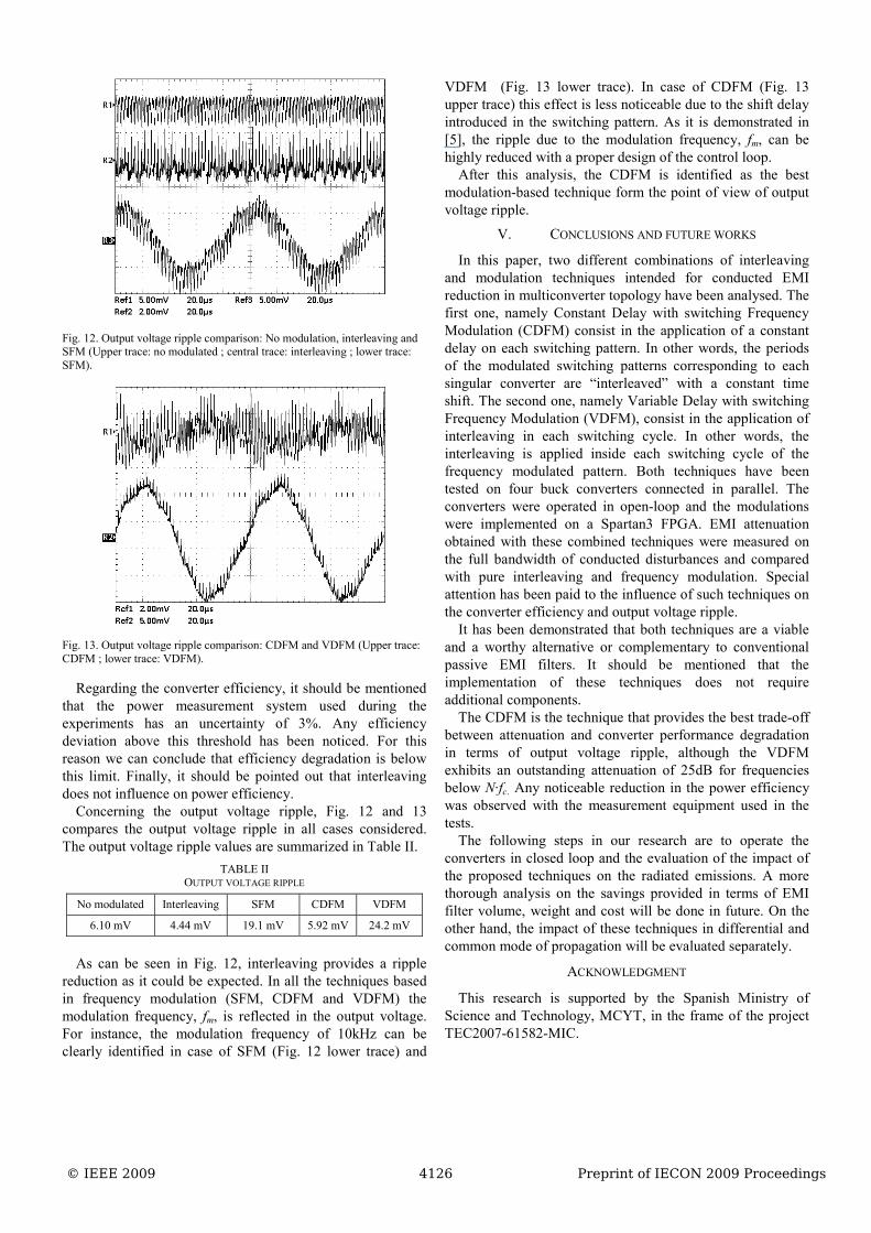
Fig. 12. Output voltage ripple comparison: No modulation, interleaving and SFM (Upper trace: no modulated ; central trace: interleaving ; lower trace: SFM).
Fig. 13. Output voltage ripple comparison: CDFM and VDFM (Upper trace: CDFM ; lower trace: VDFM).
Regarding the converter efficiency, it should be mentioned that the power measurement system used during the experiments has an uncertainty of 3%. Any efficiency deviation above this threshold has been noticed. For this reason we can conclude that efficiency degradation is below this limit. Finally, it should be pointed out that interleaving does not influence on power efficiency.
Concerning the output voltage ripple, Fig. 12 and 13 compares the output voltage ripple in all cases considered. The output voltage ripple values are summarized in Table II.
TABLE II OUTPUT VOLTAGE RIPPLE
No modulated Interleaving SFM CDFM VDFM
6.10 mV 4.44 mV 19.1 mV 5.92 mV 24.2 mV
As can be seen in Fig. 12, interleaving provides a ripple
reduction as it could be expected. In all the techniques based in frequency modulation (SFM, CDFM and VDFM) the modulation frequency, fm, is reflected in the output voltage. For instance, the modulation frequency of 10kHz can be clearly identified in case of SFM (Fig. 12 lower trace) and
VDFM (Fig. 13 lower trace). In case of CDFM (Fig. 13 upper trace) this effect is less noticeable due to the shift delay introduced in the switching pattern. As it is demonstrated in [5], the ripple due to the modulation frequency, fm, can be highly reduced with a proper design of the control loop.
After this analysis, the CDFM is identified as the best modulation-based technique form the point of view of output voltage ripple.
V. CONCLUSIONS AND FUTURE WORKS
In this paper, two different combinations of interleaving and modulation techniques intended for conducted EMI reduction in multiconverter topology have been analysed. The first one, namely Constant Delay with switching Frequency Modulation (CDFM) consist in the application of a constant delay on each switching pattern. In other words, the periods of the modulated switching patterns corresponding to each singular converter are “interleaved” with a constant time shift. The second one, namely Variable Delay with switching Frequency Modulation (VDFM), consist in the application of interleaving in each switching cycle. In other words, the interleaving is applied inside each switching cycle of the frequency modulated pattern. Both techniques have been tested on four buck converters connected in parallel. The converters were operated in open-loop and the modulations were implemented on a Spartan3 FPGA. EMI attenuation obtained with these combined techniques were measured on the full bandwidth of conducted disturbances and compared with pure interleaving and frequency modulation. Special attention has been paid to the influence of such techniques on the converter efficiency and output voltage ripple.
It has been demonstrated that both techniques are a viable and a worthy alternative or complementary to conventional passive EMI filters. It should be mentioned that the implementation of these techniques does not require additional components.
The CDFM is the technique that provides the best trade-off between attenuation and converter performance degradation in terms of output voltage ripple, although the VDFM exhibits an outstanding attenuation of 25dB for frequencies below N·fc. Any noticeable reduction in the power efficiency was observed with the measurement equipment used in the tests.
The following steps in our research are to operate the converters in closed loop and the evaluation of the impact of the proposed techniques on the radiated emissions. A more thorough analysis on the savings provided in terms of EMI filter volume, weight and cost will be done in future. On the other hand, the impact of these techniques in differential and common mode of propagation will be evaluated separately.
ACKNOWLEDGMENT
This research is supported by the Spanish Ministry of Science and Technology, MCYT, in the frame of the project TEC2007-61582-MIC.
© IEEE 2009 4126 Preprint of IECON 2009 Proceedings
REFERENCES [1] Feng Lin and Chen, D.Y., “Reduction of Power Supply EMI Emission
by Switching Frequency Modulation”, IEEE Trans. on Power Electronics, vol. 9, pp. 132 – 137, January 1994.
[2] Stankovic, A.M., Verghese, G.E. and Perreault, D.J., “Analysis and Synthesis of Randomized Modulation Schemes for Power Converters”, IEEE Trans. on Power Electronics, vol. 10, pp. 680 – 693, November 1995.
[3] Tse, K.K., Henry Shu-Hung Chung, Ron Hui, S.Y. and So, H.C., “A comparative study of carrier-frequency modulation techniques for conducted EMI suppression in PWM converters”, IEEE Trans. on Industrial Electronics, vol. 49, pp. 618 – 627, June 2002.
[4] Balcells J., Santolaria A., Orlandi A., Gonzalez D. and Gago J., “EMI reduction in switched power converters using frequency Modulation techniques”, IEEE Trans. on Electromagnetic Compatibility, vol. 47, pp. 569 – 576, August 2005.
[5] Gonzalez, D., Balcells, J., Santolaria, A., Le Bunetel, J-Ch., Gago, J., Magnon, D. and Brehaut, S., “Conducted EMI Reduction in Power Converters by Jeans of Periodic Switching Frequency Modulation”, IEEE Trans. On Power Electronics, vol. 22, pp. 2271–2281, November 2007.
[6] Gonzalez, D., Bialasiewicz, J-T., Balcells, J. and Gago, J., “Wavelet-Based Performance Evaluation of Power Converters Operating With Modulated Switching Frequency”, IEEE Trans. on Industrial Electronics, vol. 55, pp. 3167 – 3176, August 2008.
[7] Johnson, S. and Zane, R., “Custom spectral shaping for EMI reduction in high-frequency inverters and ballasts”, IEEE Trans. on Power Electronics, vol. 20, pp. 1499 – 1505, November 2005.
[8] Barragan, L., Navarro, D., Acero, J., Urriza, I. and Burdío, J-M., “FPGA Implementation of a Switching Frequency Modulation Circuit for EMI Reduction in Resonant Inverters for Induction Heating
Appliances”, IEEE Trans. on Industrial Electronics, vol. 55, pp. 11 – 20, January 2008.
[9] Kim, J., Kam, D. -G., Jun, P. and Kim, J., “Spread Spectrum Clock Generator With Delay Cell Array to Reduce Electromagnetic Interference”, IEEE Trans. on Electromagnetic Compatibility, vol. 47, pp. 908-920, November 2005.
[10] Chang, C. and Knights, M., “Interleaving technique in distributed power conversion systems”, IEEE Trans. on Circuits and Syst. I, vol. 42, pp. 245–251, May 1995.
[11] Zumel P., Garcia O., Cobos J.A. and Uceda J., “EMI reduction by interleaving of power converters”, Applied Power Electronics Conference and Exposition, APEC 2004, vol. 2, pp. 688 – 694, 2004.
[12] Al-Haddad K. and Rajagopalan V., “Analysis and Simulation of Multiple Converter Operation to Reduce Losses and EMI”, IEEE Workshop on Computers in Power Electronics, pp. 183 – 188, August 2004.
[13] Jayawant, S. and Jian Sun, “Double-Integral Fourier Analysis of Interleaved Pulse Width Modulation”, IEEE COMPEL Workshop, Rensselaer Polytechnic Institute, Troy, NY, USA, pp. 34 – 39, July 2006.
[14] Ozeri S., Shmilovitz D., Singer S. and Martinez-Salamero L., “The Mathematical Foundation of Distributed Interleaved Systems”, IEEE Trans. on Circuits and Systems--I: vol. 54, pp. 610-619, March 2007.
[15] Mon, J., Gonzalez, D., Gago, J. and Balcells, J., “Combined application of interleaving and modulation techniques in multiconverter topology”, IEEE International Conference on Electronics, Circuits and Systems, ICECS 2008, pp. 1087-1090.
[16] Mon, J., Gago, J., Gonzalez, D., Balcells, J., Fernandez, R. and Gil, I., “A new switching frequency modulation scheme for EMI reduction in multiconverter topology”, European Conference on Power Electronics and Applications, EPE 2009. Barcelona, September 2009.
© IEEE 2009 4127 Preprint of IECON 2009 Proceedings


