Embed Size (px)
Citation preview

IEEE TRANSACTIONS ON POWER ELECTRONICS, VOL. 25, NO. 3, MARCH 2010 775
A Passive Lossless Snubber Applied to the AC–DCInterleaved Boost Converter
Carlos Alberto Gallo, Fernando Lessa Tofoli, and Joao Antonio Correa Pinto
Abstract—High switching frequency operation of static powerconverters is often required to reduce size, weight, and electromag-netic interference levels, at the cost of increased switching lossesand reduced efficiency. Switching losses include the current andvoltage overlap loss during the switching interval and the capaci-tance loss during turn-on. Recently, the use of passive soft switch-ing methods has been emphasized as a better alternative to activemethods, mainly because they do not require extra switches oradditional control circuitry. This paper proposes a passive losslesssnubber applied to the interleaved boost converter. The use of a softcommutation cell causes the main switches to be turned on and offunder null current and null voltage conditions, respectively, as highefficiency results over the entire load range. The theoretical analy-sis including the description of the operating stages and the designprocedure are included. Experimental results on a 2 kW prototypeare presented and discussed to validate the proposal.
Index Terms—Interleaving techniques, passive snubbers, powerfactor correction, soft switching.
I. INTRODUCTION
IN ORDER to meet the requirements in the proposed stan-dards such as IEC 61000-3-2 and IEEE Std 519 on the
quality of the input current that can be drawn by low-powerequipment, a power factor correction (PFC) circuit is typi-cally added at the utility interface of an ac–dc switch-modepower supply. The boost PFC circuit operating in continu-ous conduction mode (CCM) is by far the popular choicefor medium and high power (400 W to a few kilowatts)application.
Numerous boost-type topologies have been proposed overthe past few years with the aim of improving the characteris-tics of the traditional converter, such as the reverse recoveryproblem of the boost diode [1], [2] and increase of the out-put voltage [3]. However, as the power rating increases, it isoften required to associate converters in series or in parallel.In high-power applications, interleaving of two boost convert-ers is very often employed to improve performance and reducesize of the PFC front end. Besides, for high current applica-tions and voltage step-up, the currents through the switches
Manuscript received November 5, 2008; revised March 10, 2009 and July 24,2009. Current version published April 2, 2010. Recommended for publicationby Associate Editor P. Jain.
C. A. Gallo is with the Department of Mechanical Engineering, FederalUniversity of Uberlandia, CEP 38400-902 Uberlandia, MG, Brazil (e-mail:[email protected]).
F. L. Tofoli is with the Department of Electrical Engineering, Federal Univer-sity of Sao Joao del-Rei, CEP 36307-352 Sao Joao del-Rei, MG, Brazil (e-mail:[email protected]).
J. A. C. Pinto is with the Department of Electrical Engineering, Federal In-stitute of Education, Science and Technology of Para, CEP 66.240-260 Belem,PA, Brazil (e-mail: [email protected]).
Digital Object Identifier 10.1109/TPEL.2009.2033063
become just fractions of the input current [4]. Besides, inter-leaving effectively doubles the switching frequency and alsopartially cancels the input and output ripples, as the size of theenergy storage inductors and differential-mode electromagneticinterference (EMI) filter in interleaved implementations can bereduced [5]–[12].
Reduction of size, weight, cost, and EMI in static power con-verters can be obtained by increasing the switching frequency.However, appreciable switching losses may result, compromis-ing the overall efficiency. In front of such limitation, soft switch-ing using resonant techniques is an attractive approach, whilesoft switching using lossless snubbers also gives an effective so-lution from the viewpoint of converter efficiency and extendedutilization of power switching devices [13]–[15].
Power semiconductor devices commutate under two possiblesituations: hard and soft. With hard switching, the devices aresupposed to change the states (ON or OFF) when both currentand voltage are not null. High switching stresses are due to theoverlap between voltage and current, and high switching lossesresult [16]. Soft switching is supposed to reduce the mentionedoverlap between voltage and current during the commutation,and can be classified in either active or passive methods, as onemust choose between the aforementioned snubbers for a givenapplication.
Active methods can reduce the switching losses by using aux-iliary switches. Unfortunately, an auxiliary switch increases thecomplexity of both power and control circuits. Synchroniza-tion problems between control signals of the switches duringtransient also complicate the control strategy. Circuit cost is in-creased and reliability is affected by using active snubbers [17].
A passive lossless snubber can effectively restrict switchinglosses and EMI noise using no active components and no powerdissipative components. No additional control is needed and nocirculating energy is generated. Circuit structure is as simpleas RCD snubbers while circuit efficiency is as high as activesnubbers and resonant converters [18], [19]. Low cost, highperformance, and high reliability are the distinct advantages ofa passive lossless snubber [20].
Within this context, this paper presents a soft switching ac–dcinterleaved boost converter, as a passive snubber with reducedcomplexity and low cost if compared with active circuits isintroduced. The proposed structure is better recommended forhigh current applications, where a conventional boost convertermay not be adequate [21]. The converter is discussed in de-tail, as the study is concerned with the operating principles,mathematical analysis, and experimental results on a 2 kW pro-totype. As it will be seen, significant advantages are achievedover the conventional interleaved boost converter by using thistopology.
0885-8993/$26.00 © 2010 IEEE
Authorized licensed use limited to: UNIVERSIDADE FEDERAL DE SAO JOAO DEL REI. Downloaded on April 12,2010 at 19:01:16 UTC from IEEE Xplore. Restrictions apply.

776 IEEE TRANSACTIONS ON POWER ELECTRONICS, VOL. 25, NO. 3, MARCH 2010
Fig. 1. Interleaved boost converter operating with average current mode control.
II. PROPOSED AC–DC INTERLEAVED BOOST CONVERTER
The ac–dc interleaved boost converter is shown in Fig. 1.It operates with the average current mode control, whichcan be implemented with a PFC dedicated IC [22]. Anoptimum alternative that leads to high power levels athigh switching frequencies lies in the nondissipative snub-ber represented in the dotted line for a single boostconverter.
The components of the circuit are two diodes Dr11 andDr12 , one resonant capacitor Cr1 , and one resonant induc-tor Lr1 . At this point, it is worth to mention that the place-ment of Cr1 and Lr1 obeys criteria stated in [23] for theconception of passive lossless snubbers applied to boost-typetopologies.
An auxiliary power supply can be easily implemented fromthe converter circuit by coupling boost inductor Lb1 and inductorLf b1 , and also adding one diode Df b1 , one auxiliary capacitorCaux , and one auxiliary inductor Laux . It must be mentionedthat the absence of inductor Laux would lead to the necessityof an external voltage source for the correct operation of theproposed snubber.
Of course, the proposed snubber can be applied to the conven-tional boost converter in a simple way by using the aforemen-tioned elements. However, if the introduced concept is extendedto interleaved converters, a single auxiliary power supply is nec-essary for a given number of interleaved cells defined as i. Thatis, only one auxiliary capacitor Caux and one auxiliary inductorLaux are necessary, as a single cell is used for the implementa-tion of the power supply, although one boost inductor Lbi , oneinductor Lf bi , and one diode Df bi are required per interleavedcell, what can be seen in Fig. 1.
The derived circuit is responsible for providing energy to theresonance, with the consequent achievement of soft switchingfor the main switches during both turning on and turning off.Besides, the power supply can also be employed to feed the con-trol circuitry without the need of additional auxiliary voltages.By interleaving the converters, the converter is always supposedto provide energy to the auxiliary power supply, even when dutycycle is low.
Although the number of components seems rather large im-plying increased cost and volume, complexity is reduced if com-pared with the solution proposed in [17], where two auxiliaryactive switches are used, but the number of components is re-duced. Other interleaved boost-type converters that employ ac-tive switches are presented in [24], [25], and [26].
Even though conduction losses tend to increase if comparedwith the traditional hard topology, the current flows through atmost three semiconductor elements simultaneously (disregard-ing the diodes of the rectifier bridge) in any of the operatingstages. As it will be seen in Section III, the application of thesnubber cell is justified by the appreciable increase in the effi-ciency of the converter operating at high frequency.
A. Operating Principle
In order to study the proposed topology, the following condi-tions are assumed:
1) all switches and diodes are ideal;2) input voltage Vi is constant and output voltage Vo is ripple
less over one switching period;3) inductors and capacitors are lossless and the output current
is continuous during the operation.
Authorized licensed use limited to: UNIVERSIDADE FEDERAL DE SAO JOAO DEL REI. Downloaded on April 12,2010 at 19:01:16 UTC from IEEE Xplore. Restrictions apply.

GALLO et al.: PASSIVE LOSSLESS SNUBBER APPLIED TO THE AC–DC INTERLEAVED BOOST CONVERTER 777
By definition, the following expressions are valid:
ωo1 =1√
Cr1Laux(1)
ωo2 =1√
Cr1Lr1(2)
ωo3 =1√
Cr1 (Lr1 + Laux)(3)
α =Io
Vaux
√Laux
Cr1(4)
K =Vo
Vaux(5)
K1 =Vdc1
Vaux(6)
K2 =1 − K
1 + K1(7)
K3 =Vdc2
Vaux(8)
Kb =(
1 + K1
K − 1
)√1 − K2
2 (9)
Kd =Kf
D+
2K
α(10)
Ke =1 + K1
α(11)
Kf =fs
ω01(12)
Km = Kd cos−1 K2 +Kb (K − 1)
α(13)
Lr1 =Laux
2(14)
whereωo1 resonance frequency between capacitor Cr1 and
inductor Laux in the first stage [rad/s];ωo2 resonance frequency between capacitor Cr1 and
inductor Lr1 in the fourth stage [rad/s];ωo3 resonance frequency between capacitor Cr1 , in-
ductor Lr1 and inductor Laux in the fifth stage[rad/s];
α normalized load current [A];Io load current [A];Vaux voltage across auxiliary capacitor Caux [V];Vdc1 , Vdc2 initial and final values of the voltage across ca-
pacitor Cr1 in the fifth stage, respectively [V].The operation of the converter shown in Fig. 1 considering
the positive half cycle of the input voltage is divided in sixstages, according to Fig. 2. The main waveforms that describethe behavior of the circuit are shown in Fig. 3.
A single cell is analyzed due to the inherent analogy betweenthe converter legs. Besides, the cells in the interleaved boostconverter do not operate simultaneously. In fact, the switchinginstants are sequentially phased over fractions of the switching
period. In this case, where two conventional boost convertersare interleaved, the maximum duty cycle for each main switchis equal to D = 0.5. For this reason, resonances in two cells donot occur at the same time. Then, the converter uses only oneauxiliary capacitor Caux and one auxiliary inductor Laux , whichtake part in the operation of one single cell at a time.
First stage (t0 , t1): Before this stage begins, switch S1 is offand energy is transferred to the load by the source, analogouslyto the traditional boost converter, although the current flowsthrough both inductors Lb1 and Lr1 . When this stage effectivelybegins, switch S1 is turned on under null current condition,because inductor Lr1 is linearly discharged through the loopinvolving Co/Ro , Db1 , and S1 . The auxiliary power supplymaintains the resonance between Laux and Cr1 , what persistsuntil the voltage across capacitor Cr1 equals the output voltageVo , causing diode Dr12 to be forward biased.
It can be demonstrated that the current through inductor Lauxis given by
iLa u x (t) =√
Cr1
Laux(Vaux + Vdc1) sinω01t. (15)
The voltage across capacitor Cr1 is given by
vCr 1 (t) = Vaux − (Vaux + Vdc1) cos ω01t. (16)
The time interval that defines this stage is
∆t1 = t1 − t0 =arccos K2
ω01. (17)
Second stage (t1 , t2): While switch S1 is still on, the voltageacross capacitor Cr1 remains constant and clamped to Vo . In-ductor Laux is linearly discharged through the loop formed byDr11 ,Dr12 , Co/Ro , and the auxiliary power supply. This stageis responsible for the pulsewidth modulation (PWM) character-istics of the converter, and it finishes when switch S1 is turnedOFF.
The current through inductor Laux is
iLa u x (t) = − (Vo − Vaux)Laux
t +√
Cr1
Laux(Vdc1 +Vaux)
√1−K2
2 .
(18)The time interval that defines this stage is
∆t2 = t2 − t1 =1
ω01
(1 + K1
K − 1
) √1 − K2
2 . (19)
Third stage (t2 , t3): While previously charged at Vo , reso-nant capacitor Cr1 is now linearly discharged through the loopformed by Lb1 , Co/Ro , and Dr12 , allowing switch S1 is turnedoff with null voltage in this stage.
The voltage across Cr1 is
vCr 1 (t) = − I0
Cr1t + V0 . (20)
The time interval that corresponds to this stage is
∆t3 = t3 − t2 =Cr1Vo
Io. (21)
Fourth stage (t3 , t4): There is resonance between inductorLr1 and capacitor Cr1 , as the current through Lr1 equals the
Authorized licensed use limited to: UNIVERSIDADE FEDERAL DE SAO JOAO DEL REI. Downloaded on April 12,2010 at 19:01:16 UTC from IEEE Xplore. Restrictions apply.

778 IEEE TRANSACTIONS ON POWER ELECTRONICS, VOL. 25, NO. 3, MARCH 2010
Fig. 2. Operating stages. (a) First stage (t0 , t1 ). (b) Second stage (t1 , t2 ). (c) Third stage (t2 , t3 ). (d) Fourth stage (t3 , t4 ). (e) Fifth stage (t4 , t5 ).(f) Sixth stage (t5 , t6 ).
load current Io and capacitor Cr1 is negatively charged at theend of this stage.
The behavior of the current through Lr1 and the voltage acrossCr1 can be expressed as
iLr 1 (t) = I0 (1 − cos ω02t) (22)
vCr 1 (t) = Lr1I0ω02 sen ω02t. (23)
The time interval that defines this stage is
∆t4 = t4 − t3 =3π
2ω02. (24)
Fifth stage (t4 , t5): Resonance between capacitor Cr1 andinductors Laux and Lr1 occurs through the loop formed byDb1 , Co/Ro,Dr11 , and the auxiliary power supply. This stagefinishes when the current through Lr1 equals the load currentIo .
The current through inductor Laux is
iLa u x (t) = Cr1ω03 [(Vaux − V0) − Vdc2 ] sin ω03t. (25)
The voltage across capacitor Cr1 is
vCr 1 (t) = − [(Vaux − Vo) − Vdc2 ] cos ω03t. (26)
The time interval that defines this stage is
∆t5 = t5 − t4 =π
ω03. (27)
Sixth stage (t5 , t6): The voltage across resonant capacitorCr1 is clamped to the voltage assumed at the end of the previ-ous resonant stage, until a new switching cycle begins. Boostinductor Lb1 provides energy to the load, as the operation of aconventional boost converter is observed.
The time interval that defines this stage is
∆t6 = Ts − (∆t1 + ∆t2 + ∆t3 + ∆t4 + ∆t5) (28)
where Ts is the switching period.
Authorized licensed use limited to: UNIVERSIDADE FEDERAL DE SAO JOAO DEL REI. Downloaded on April 12,2010 at 19:01:16 UTC from IEEE Xplore. Restrictions apply.

GALLO et al.: PASSIVE LOSSLESS SNUBBER APPLIED TO THE AC–DC INTERLEAVED BOOST CONVERTER 779
Fig. 3. Main theoretical waveforms.
B. Static Gain of The Converter
By definition, the static gain of the converter is
G =Vo
Vi. (29)
The gain can be obtained from the voltage across inductorLb1 , when it is equal to the difference between the input voltageVi and the output voltage V0 . While there is resonance and/orcapacitor Cr1 is charged, the voltage across Lb1 will always bedifferent from Vi − V0 . When switch S1 is turned on, inductorLb1 is charged and the following expression is valid:
vLb1(t) = Lb1diLb1(t)
dt. (30)
Since inductor Lb1 is charged linearly, expression (30) can besimplified as
vLb1 = Lb1∆iLb1
∆t(31)
where
vLb1 = Vi (32)
∆iLb1 = Imax − Imin = I0 (33)
∆t = ∆t2 = (t2 − t1) = DTs (34)
where Imax and Imin are the upper and lower limits of the currentthrough inductor Lb1 , considering the operation of the converterin CCM, ∆t is the interval that corresponds to the second stage,and D is the duty cycle.
Substituting (32)–(34) in (30) gives
Vi
Lb1=
Io
DTs. (35)
Fig. 4. Duty cycle versus normalized load current.
When switch S1 is turned off, inductor Lb1 is discharged.The interval during which the voltage across Lb1 is V0 − Vi isdefined as ∆t′
∆t′ = (1 − D) Ts − [∆t3 + ∆t4 + ∆t5 ] . (36)
The voltage across Lb1 during ∆t′ is
(Vo − Vi) = Lb1Io
∆t′. (37)
From (35), one can obtain
Lb1 =ViDTs
I0. (38)
Substituting (38) in (37) gives
(V0 − Vi) =DTsVi
∆t′. (39)
Dividing both sides of (39) by Vi and rearranging it in termsof (29), one can obtain the static gain as
G = 1 +DTs
∆t′. (40)
Expanding (40), the static gain can be finally expressed as
G = 1 +D
(1 − D) − fs
ω0 1
[Kα + π
(3
2√
2+
√32
)] (41)
where fs is the switching frequency.From (41), one can plot the curves in Fig. 4, where the duty
cycle behavior is a function of the normalized current, for severalvalues of the static gain. If α < 1, the output characteristic of theconverter is similar to that of a quasi-resonant converter [24].Otherwise if α ≥ 1, the output characteristic is the same of aPWM boost topology.
C. Analysis of Semiconductor Elements
The cells that constitute the interleaved boost converter oper-ate analogously. Therefore, one can obtain the expressions fordetermining the stress of the semiconductor elements consider-ing a single cell, what is detailed as follows.
Authorized licensed use limited to: UNIVERSIDADE FEDERAL DE SAO JOAO DEL REI. Downloaded on April 12,2010 at 19:01:16 UTC from IEEE Xplore. Restrictions apply.

780 IEEE TRANSACTIONS ON POWER ELECTRONICS, VOL. 25, NO. 3, MARCH 2010
Fig. 5. Average current through switch S1 .
1) Main Switch S1: Switch S1 remains turned on duringthe first and second stages considering its respective switchingcycle. By summing the average currents through the switch inboth stages, one can obtain the total average current as (42),while Fig. 5 represents it plotted as a function of parameterα. One can see that the converter behaves as a quasi-resonantconverter for low values of α. High average currents result thenbecause the resonant tank provides a considerable amount of thetotal load current. When α is high enough, the resonant currentis reduced at the cost of high duty cycle.
IS1(avg .)
I0=
(Kf Kb)2
2D+ Kf Kb
[Kf
D+
2K
α+
KB (K − 1)α
]
+Kf
(Kf
2D+
K
α
)cos−1K2 +Kf
[2K − 1
α+
√2
2
].
(42)
Analogously, the normalized rms current through switch S1can be determined as
I2S1(rms)
I20
=Kf K2
d
(cos−1 K2
)3
3+ 2Kf KdKe
×[(1 − K2) cos−1 K2 +
√1 − K2
2
]+ Kf KbKm
+Kf K2
e
2
[cos−1 K2 − K2
√1 − K2
2
]
+(Kf Kb)
3
3D2 +(Kf Kb)
2 Km
D. (43)
Fig. 6 shows the rms current through the main switch as afunction of α, which assumes a pattern similar to that observedin Fig. 5.
2) Diode Db1: Current flows through diode Db1 during thefirst, fourth, fifth, and sixth stages, as the total average currentthrough it is calculated from (44) and plotted in Fig. 7. One can
Fig. 6. RMS current through switch S1 .
Fig. 7. Average current through diode Db1 .
see that the average current increases significantly when α is low,evidencing the contribution of the resonant circuit to the loadcurrent, such as in quasi-resonant converters. When α is high,the converter assumes the characteristic of a classical PWMtopology, as the normalized average current tends to increasewhen α also does
IDb1(avg .)
I0= 1 − Kf
[K
α
((cos−1 K2
)2 + 1)
+ 2K1 + Kb −1√2
]. (44)
Authorized licensed use limited to: UNIVERSIDADE FEDERAL DE SAO JOAO DEL REI. Downloaded on April 12,2010 at 19:01:16 UTC from IEEE Xplore. Restrictions apply.

GALLO et al.: PASSIVE LOSSLESS SNUBBER APPLIED TO THE AC–DC INTERLEAVED BOOST CONVERTER 781
Fig. 8. Rms current through diode Db1 .
Analogously, the rms current through Db1 is given by (45)and graphically represented by Fig. 8. The same characteristicassumed by the average current is also observed
I2Db1(rms)
I20
=1+Kf
{2K
(cos−1K2
)2[2K cos−1 −1]
+3π+84√
2+ K1
(π
√23− 4
)−Kb−
K
α
}.
(45)
3) Diode Dr11: Current flows through diode Dr11 duringthe first and second stages. The average current through thisdiode can be obtained by (46) and plotted as Fig. 9. One can seethat the average current is low when α also is, since the converterassumes the characteristic of a quasi-resonant topology. When αis high, the contribution of the resonant tank to the load currentbecomes negligible
I2Dr11(avg .)
I20
=Kf
α
[K1 + K +
K2b (3 − K)
2
]. (46)
The rms current through diode Dr11 is given by (47), and therespective graph is represented in Fig. 10. The same behaviorobserved in Fig. 9 is also verified in this case
I2Dr11(rms)
I20
=Kf
α2
{(1 + K1)
2
2
[cos−1 K2 − K2
√1 − K2
2
]
+ K3b
[(K − 1)2
3− (K − 1) + 1
]}.
(47)
Fig. 9. Average current through diode Dr 11 .
Fig. 10. RMS current through diode Dr 11 .
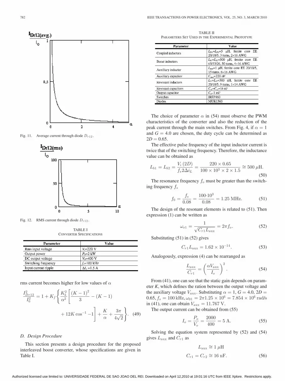
4) Diode Dr12: Current flows through diode Dr12 duringthe second, third, and fourth stages. The resulting average cur-rent through this element can be obtained by (48), which can beplotted as Fig. 11. One can see that the average current tendsto be constant when α > 1, which is a typical characteristic ofPWM converters. If α � 1, the resonant current becomes signif-icant, as the converter assumes the behavior of a quasi-resonantstructure
IDr12(avg .)
I0= Kf
[K2
b (3 − K)2α
− K
α− 1√
2
]. (48)
Analogously, the rms current through Dr12 can be determinedfrom (49), and the respective curve is shown in Fig. 12. The samebehavior developed by the average current is observed, as the
Authorized licensed use limited to: UNIVERSIDADE FEDERAL DE SAO JOAO DEL REI. Downloaded on April 12,2010 at 19:01:16 UTC from IEEE Xplore. Restrictions apply.
782 IEEE TRANSACTIONS ON POWER ELECTRONICS, VOL. 25, NO. 3, MARCH 2010
Fig. 11. Average current through diode Dr 12 .
Fig. 12. RMS current through diode Dr 12 .
TABLE ICONVERTER SPECIFICATIONS
rms current becomes higher for low values of α
I2Dr12
I20
= 1 + Kf
{K2
b
α2
[(K − 1)2
3− (K − 1)
+ 12K cos−1 −1
]+
K
α+
3π
4√
2
}. (49)
D. Design Procedure
This section presents a design procedure for the proposedinterleaved boost converter, whose specifications are given inTable I.
TABLE IIPARAMETERS SET USED IN THE EXPERIMENTAL PROTOTYPE
The choice of parameter α in (54) must observe the PWMcharacteristics of the converter and also the reduction of thepeak current through the main switches. From Fig. 4, if α = 1and G = 4.0 are chosen, the duty cycle can be determined as2D = 0.65.
The effective pulse frequency of the input inductor current istwice that of the switching frequency. Therefore, the inductancevalue can be obtained as
Lb1 = Lb2 =Vi (2D)fs2∆iL
=220 × 0.65
100 × 103 × 2 × 1.5∼= 500 µH.
(50)The resonance frequency fo must be greater than the switch-
ing frequency fs
f0 =fs
0.08=
100·103
0.08= 1.25 MHz. (51)
The design of the resonant elements is related to (51). Thenexpression (1) can be written as
ωo1 =1√
Cr1Laux= 2πfo. (52)
Substituting (51) in (52) gives
Cr1Laux = 1.62 × 10⁻¹⁴ . (53)
Analogously, expression (4) can be rearranged as
Laux
Cr1=
(αVaux
Io
)2
. (54)
From (41), one can see that the static gain depends on param-eter K, which defines the ration between the output voltage andthe auxiliary voltage Vaux . Substituting α = 1, G = 4.0, 2D =0.65, fs = 100 kHz, ω01 = 2π1.25 × 106 = 7.854 × 10⁶ rad/sin (41), one can obtain Vaux = 11.767 V.
The output current can be obtained from (55)
Io =Po
Vo=
2000400
= 5 A. (55)
Solving the equation system represented by (52) and (54)gives Laux and Cr1 as
Laux ∼= 1 µH
Cr1 = Cr2 ∼= 16 nF. (56)
Authorized licensed use limited to: UNIVERSIDADE FEDERAL DE SAO JOAO DEL REI. Downloaded on April 12,2010 at 19:01:16 UTC from IEEE Xplore. Restrictions apply.

GALLO et al.: PASSIVE LOSSLESS SNUBBER APPLIED TO THE AC–DC INTERLEAVED BOOST CONVERTER 783
Fig. 13. Input voltage and input current at rated load. (a) Light load (250 W). Scales: Vi 100 V/div.; Ii 1 A/div.; time 5 ms/div. Power factor = 0.981 THDV =3.78%; THDI = 7.36%. (b) Rated load (2 kW). Scales: Vi 100 V/div.; Ii 5 A/div.; time 5 ms/div. Power factor = 0.998; THDV = 3.34%; THDI = 5.76%.
Fig. 14. Drain-to-source voltage and current waveforms of switch S1 withoutusing the proposed snubber. Scales: VS 1 200 V/div.; IS 1 4 A/div.; time 2 µs/div.
It must be also mentioned that inductor Lr1 can be determinedfrom expression (14)
Lr1 = Lr2 =1 × 10⁻⁶
2= 500 nH. (57)
III. EXPERIMENTAL RESULTS
An experimental prototype of the converter was implementedusing the parameters set shown in Table II. Results are discussedas follows. It must be also mentioned that the waveforms rep-resented in Figs. 14–17 were acquired around the peak inputvoltage.
Power factor correction for light load and rated load condi-tions is evidenced in Fig. 13(a) and (b), respectively. It alsodemonstrates that the use of the average current mode control isefficient causing the minimization of the total harmonic distor-tion of the input current.
Fig. 14 presents the relevant waveforms of main switch S1 ,where hard commutation is verified, causing appreciable switch-ing losses and compromising the converter efficiency.
Fig. 15 shows the soft commutation of switch S1 , which isturned on and off under zero current and zero voltage conditions,respectively, in both light and rated load conditions. Addition-ally, there are not high current and voltage peaks when the switchis turned on or off, respectively.
Fig. 16 presents the relevant waveforms regarding the reso-nant elements, which are similar to those predicted in the theo-retical analysis.
Fig. 17 shows the currents through boost inductors Lb1 andLb2 , where good current sharing between the interleaved con-verters is verified.
Fig. 18 presents the input power factor as a function of theoutput power. The curve shows that high power factor is obtainedalong the entire load range. One can see that power factor is0.998 at rated load, what is in according with the waveformsshown in Fig. 13.
Finally, Fig. 19 shows the efficiency curves of the converteroperating at 100 kHz with and without the passive snubber.As the output power increases, efficiency tends to decrease inthe hard topology, which was evaluated to 2 kW, due to theappreciable conduction and switching losses. It can be seen thatefficiency is significantly increased by the snubber for almost theentire load range, being higher than 98% at rated load. It mustbe also mentioned that such characteristic of the converter canbe further improved if MOSFETs with reduced on-resistanceare employed.
Although the structure presented in [29] introduces a pas-sive snubber with reduced number of components, efficiencyat rated load is about 3% less than that of the converter pro-posed in this paper, where rated output power is 400 W andswitching frequency is 40 kHz. According to Table II, theprototype implemented in this paper is rated at 2 kW op-erating at 100 kHz. One can see in Fig. 19 that efficiencyat 400 W is almost the same, even though switching fre-quency is 2.5 times greater than that of the prototype designedin [29].
Another fair comparison can be established considering thetopology presented in [30], where a simple circuit with cou-pled inductors is proposed, with maximum efficiency of 92.6%.Even though there are few components in the passive loss-less clamp circuit, the switching frequency is 50 kHz. Sincethe experimental prototype specified in Table II operates at100 kHz, high efficiency and reduction of size and volume ofmagnetics can be considered as prominent characteristics of theconverter.
Authorized licensed use limited to: UNIVERSIDADE FEDERAL DE SAO JOAO DEL REI. Downloaded on April 12,2010 at 19:01:16 UTC from IEEE Xplore. Restrictions apply.

784 IEEE TRANSACTIONS ON POWER ELECTRONICS, VOL. 25, NO. 3, MARCH 2010
Fig. 15. Drain-to-source voltage and current waveforms of switch S1 using the proposed snubber. (a) Light load (250 W). Scales: VS 1 200 V/div.; IS 1 2 A/div.;time 1 µs /div. (b) Rated load (2 kW). Scales: VS 1 200 V/div.; IS 1 4 A/div.; time 1 µs/div.
Fig. 16. Waveforms of the resonant elements. Scales: IL a u x 4 A/div.; IL r 1 :2 A/div.; VC r 1 : 200 V/div.; time: 1.5 µs/div.
Fig. 17. Current through the boost inductors. Scales: ILb1 , ILb2 2 A/div.; time10 µs/div.
Fig. 18. Power factor versus output power.
Fig. 19. Efficiency versus output power.
IV. CONCLUSION
This paper has reported analytical and experimental resultson a passive soft switching circuit applied to the interleavedboost converter. It has been demonstrated that the structure pro-vides highly efficient power factor correction with negligiblecommutation losses, using the same number of switches of thehard-switched structure.
The cell provides zero current switching for the main switchesat turning on and zero voltage switching during turning off. Theaccurate operation of the circuit is validated by implementingand evaluating an experimental prototype. Efficiency tends tobe quite high if compared with the conventional hard topologyor similar approaches existent in the literature, even at highfrequency operation or high power levels. The number of com-ponents can be seen as a drawback if the topology is comparedto other interleaved boost converters. However, it must be men-tioned that the converter efficiency at high frequency operation issignificantly increased for a wide load range, without the need ofusing additional switches or control circuitry. Besides, reducedcomplexity and increased reliability are direct advantages of theproposed circuit.
ACKNOWLEDGMENT
The authors gratefully acknowledge INCT-EIE, CAPES,CNPq, and FAPEMIG for the support to this work.
Authorized licensed use limited to: UNIVERSIDADE FEDERAL DE SAO JOAO DEL REI. Downloaded on April 12,2010 at 19:01:16 UTC from IEEE Xplore. Restrictions apply.

GALLO et al.: PASSIVE LOSSLESS SNUBBER APPLIED TO THE AC–DC INTERLEAVED BOOST CONVERTER 785
REFERENCES
[1] W. Y. Choi, J. Kwon, E. H. Kim, J. J. Lee, and B. H. Kwon, “Bridgelessboost rectifier with low conduction losses and reduced diode reverse-recovery problems,” IEEE Trans. Ind. Electron., vol. 54, no. 2, pp. 769–780, Apr. 2007.
[2] J. M. Kwon, W. Y. Choi, and B. H. Kwon, “Cost-effective boost con-verter with reverse-recovery reduction and power factor correction,” IEEETrans. Ind. Electron., vol. 55, no. 1, pp. 471–473, Jan. 2008.
[3] F. L. Tofoli, E. A. A. Coelho, L. C. de Freitas, V. J. Farias, and J. B. VieiraJr., “Proposal of a soft-switching single-phase three-level rectifier,” IEEETrans. Ind. Electron., vol. 55, no. 1, pp. 107–113, Jan. 2008.
[4] Y. Jang and M. M. Jovanovic, “Interleaved boost converter with intrinsicvoltage-doubler characteristic for universal-line PFC front end,” IEEETrans. Power Electron., vol. 22, no. 4, pp. 1394–1401, Jul. 2007.
[5] P. W. Lee, Y. S. Lee, D. K. W. Cheng, and X. C. Liu, “Steady-state analysisof an interleaved boost converter with coupled inductors,” IEEE Trans.Ind. Electron., vol. 47, no. 4, pp. 787–795, Aug. 2000.
[6] R. D. Middlebrook, “Transformerless dc-to-dc converters with large con-version ratios,” IEEE Trans. Power Electron., vol. 3, no. 4, pp. 484–488,Oct. 1988.
[7] L. R. Barbosa, J. A. Lambert, L. C. Freitas, J. B. Vieira, Jr., and V. J.Farias, “A boost PWM soft-single-switched converter with low voltageand current stresses,” IEEE Trans. Power Electron., vol. 13, no. 1, pp. 26–35, Jan. 1998.
[8] M. Veerachary, T. Senjyu, and K. Uezato, “Modeling and analysis ofinterleaved dual boost converter,” in Proc. IEEE Int. Symp. Ind. Electron.,2001, vol. 2, pp. 718–722.
[9] D. J. Perreault and J. G. Kassakian, “Distributed interleaving of paralleledpower converters,” IEEE Trans. Circuits Syst. I: Fund. Theory Appl.,vol. 44, no. 8, pp. 728–734, Aug. 1997.
[10] C. Chang and M. A. Knights, “‘Interleaving technique in distributed powerconversion systems,” IEEE Trans. Circuits Syst. I: Fund. Theory Appl.,vol. 42, no. 5, pp. 245–251, May 1995.
[11] M. T. Zhang, Y. Jianp, F. C. Lee, and M. M. Jovanovic, “Single-phasethree-level PWM power factor correction converter,” in Proc. IEEE Appl.Power Electron. Conf. Expo., 1995, pp. 434–439.
[12] B. A. Miwa, D. M. Otten, and M. F. Schlecht, “High efficiency powerfactor correction using interleaving techniques,” in Proc. Appl. PowerElectron. Conf. Expo., 1992, pp. 557–568.
[13] A. Elasser and D. A. Torrey, “Soft switching active snubbers for dc/dcconverters,” IEEE Trans. Power Electron., vol. 11, no. 5, pp. 710–722,Sep. 1996.
[14] G. Hua, C. S. Leu, and F. C. Lee, “Novel zero-voltage-transition PWMconverter,” in Proc. IEEE Power Electron. Spec. Conf., 1992, pp. 55–61.
[15] K. Taniguchi, K. Hirachi, and H. Irie, “Soft-switching circuit for three-phase converter with unity power factor,” in Proc. Inst. Elect. Eng.,vol. 117, pt. D, no. 2, pp. 142–149, 1997.
[16] C. M. O. Stein, H. L. Hey, J. R. Pinheiro, H. Pinheiro, and H. A. Grundling,“Analysis, design, and implementation of a new ZCZVT commutation cellfor PWM dc-ac converters,” in Proc. IEEE Ind. Appl. Soc. Annu. Meeting,2001, pp. 845–850.
[17] G. Yao, Y. Shen, W. Li, and X. He, “A new soft switching snubber for theinterleaved boost converters,” in Proc. 35th Annu. IEEE Power Electron.Spec. Conf., 2004, pp. 3765–3769.
[18] I. Matsuura, K. M. Smith, Jr., and K. M. Smedley, “A comparison of activeand passive switching methods for PWM converters,” in Proc. 29th Annu.IEEE Power Electron. Spec. Conf., 1998, vol. 1, pp. 94–100.
[19] G. Hua and F. C. Lee, “Soft-switching techniques in PWM converters,”IEEE Trans. Ind. Electron., vol. 42, no. 6, pp. 595–603, Dec. 1995.
[20] K. Fujiwara and H. Nomura, “A novel lossless passive snubber for soft-switching boost-type converters,” IEEE Trans. Power Electron., vol. 14,no. 6, pp. 1065–1069, Nov. 1999.
[21] J. R. Pinheiro, H. A. Grundling, D. L. R. Vidor, and J. E. Baggio, “Controlstrategy of an interleaved boost power factor correction converter,” inProc. IEEE Power Electron. Spec. Conf., 1999, pp. 137–142.
[22] P. C. Todd “UC3854 controlled power factor correction circuit design,”UNITRODE Application Note U-134.
[23] K. M. Smith, Jr. and K. M. Smedley, “Properties and synthesis of lossless,passive soft switching converters,” in Proc. 1st Int. Congr. Israel EnergyPower Motion Control, May 1997, pp. 112–119.
[24] L. R. Barbosa, B. A. Angelico, and C. H. G. Treviso, “A new interleavedboost PWM soft switched converter,” in Proc. IEEE Int. Conf. Ind. Appl.,IV Induscon, 2000, pp. 108–113.
[25] A. T. Cezar, A. A. Pereira, and L. R. Barbosa, “An interleaved boost PWMsoft switched converter without stresses,” in Proc. IEEE Int. Conf. Ind.Appl., VI Induscon, 2004, pp. 250–255.
[26] Y. Jang and M. M. Jovanovic, “Soft switching circuit for interleaved boostconverters,” IEEE Trans. Power Electron., vol. 22, no. 1, pp. 80–86, Jan.2007.
[27] D. Wang, X. He, and R. Zhao, “ZVT interleaved boost converters withbuilt-in voltage doubler and current auto-balance characteristic,” IEEETrans. Power Electron., vol. 23, no. 6, pp. 2847–2854, Nov. 2008.
[28] F. C. Lee, “High-frequency quasi-resonant converter technologies,” inProc. IEEE, Apr. 1988, vol. 76, no. 4, pp. 337–389.
[29] R. Gules, L. L. Pfitscher, and L. C. Franco, “An interleaved boostdc-dc converter with large conversion ratio,” in Proc. IEEE Int. Symp.Ind. Electron., 2003, pp. 411–416.
[30] W. Li and X. He, “An interleaved winding-coupled boost converter withpassive lossless clamp circuits,” IEEE Trans. Power Electron., vol. 22,no. 4, pp. 1499–1507, Jul. 2007.
Carlos Alberto Gallo was born in Sao Jose do RioPreto, Brazil, on June 18, 1974. He received theB.Sc., M.Sc., and Ph.D. degrees in electrical engi-neering from the Federal University of Uberlandia,Uberlandia, Brazil, in 2000, 2002, and 2005,respectively.
Currently, he is a Professor in the Depart-ment of Mechanical Engineering, Federal Universityof Uberlandia. His research interests include high-frequency power conversion, microprocessor-basedcontrol of power converters, power factor correction
topologies, and UPS systems.
Fernando Lessa Tofoli was born in Sao Paulo,Brazil, on March 11, 1976. He received the B.Sc.,M.Sc., and Ph.D. degrees in electrical engineer-ing from the Federal University of Uberlandia,Uberlandia, Brazil, in 1999, 2002, and 2005,respectively.
Currently, he is a Professor in the Departmentof Electrical Engineering, Federal Umiversity of SaoJoao del-Rei, Sao Joao del-Rei, Brazil. His researchinterests include power-quality-related issues, high-power factor rectifiers, and soft switching techniques
applied to static power converters.
Joao Antonio Correa Pinto was born in Belem,Brazil, on July 29, 1955. He received B.Sc. degreein both physics and electrical engineering from theFederal University of Para, Para, Brazil, in 1982 and1992, respectively, and the M.Sc. and Ph.D. degreesin electrical engineering from the Federal Universityof Uberlandia, Uberlandia, Brazil, in 1997 and 2002,respectively.
Currently, he is a Professor with the Departmentof Electrical Engineering, Federal Institute of Edu-cation, Science and Technology of Para,, Belem. His
research interests include high-frequency power conversion, modeling and con-trol of converters, power factor correction circuits, UPS systems, and new con-verters topologies.
Authorized licensed use limited to: UNIVERSIDADE FEDERAL DE SAO JOAO DEL REI. Downloaded on April 12,2010 at 19:01:16 UTC from IEEE Xplore. Restrictions apply.