Embed Size (px)
Citation preview

JOURNAL OF APPLIED PHYSICS VOLUME 83, NUMBER 12 15 JUNE 1998
A thermionic-emission-diffusion model for graded base Pnp heterojunctionbipolar transistors
S. Datta, K. P. Roenker,a) and M. M. CahayDepartment of Electrical and Computer Engineering, University of Cincinnati, Cincinnati, Ohio 45221-0030
~Received 2 December 1997; accepted for publication 10 March 1998!
An analytical model which matches thermionic-emission-diffusion of holes across the emitter-baseheterojunction with drift-diffusion transport across a graded base has been developed and used toexamine the performance capabilities of InP-basedPnp heterojunction bipolar transistors~HBTs!.Hole drift-diffusion across the emitter-base space charge region is shown to be of comparableimportance to thermionic emission in controlling hole injection into the base. The effects ofcompositional base grading on the recombination currents is also taken into account. Compositionalgrading of the base is shown to enhance the device’s current gain by as much as a factor of 10 byreducing recombination in the quasi-neutral base. More importantly, compositional base gradingsignificantly reduces the base transit time which improves the device’s peak cutoff frequency by asmuch as a factor of 1.5. A cutoff frequency as high as 35 GHz is found to be possible. The analysisindicates that composition grading of the base can be useful in developing high performancePnpInP-based HBTs. ©1998 American Institute of Physics.@S0021-8979~98!01112-8#
-nthiorr
re
cnfed
riccelso
icift-m
onlttdly
aseeedenseud-m-ef-is
m-nd
ults
gthe
nc-ithrier. Inlesion.ertanteto
I. INTRODUCTION
In comparison withNpn heterojunction bipolar transistors ~HBTs!, Pnp InP-based HBTs have not been extesively investigated. However, thePnp devices are of interesfor some circuit applications where they can be monolitcally integrated withNpn HBTs and used as active loadsin push-pull amplifiers.1–3 They have also shown promise fopower amplifiers.4–7 Recently, there have been severalports of successful demonstrations of InP-basedPnp HBTsoperating at microwave frequencies.8–10 Stanchinaet al.8,9
have reported InAlAs/InGaAsPnp HBTs with a currentgain as high as 170, a cutoff frequencyf T of 14 GHz, and amaximum frequency of oscillationf MAX of 22 GHz. Lunardiet al.10 have reported similar results for InP/InGaAsPnpHBTs with a current gain as high as 420, a cutoff frequenf T of 10.5 GHz, and a maximum frequency of oscillatiof MAX of 25 GHz. In addition, the monolithic integration oPnp HBTs with Npn’s has also been recently demonstratusing a selective area epitaxial growth.8 There have alsobeen some theoretical studies of the devices using numemodeling to investigate the device’s performanpotential.11,12 Finally, some encouraging results have abeen reported forPnp HBTs in the similar AlGaAs/GaAsmaterial system in recent years.13,14
This article investigates the performance of thePnpInP-based HBTs by developing an analytical thermionemission-diffusion model which matches the hole drdiffusion current at the emitter end of the quasi-neutral, copositionally graded base with the hole thermionic-emissidiffusion current across the valence band spike. The resuthen used to determine the excess hole concentration aemitter end of the base. This approach is easily extendeGaAs-basedPnp HBTs and is analogous to that previous
a!Electronic mail: [email protected]
8030021-8979/98/83(12)/8036/10/$15.00
Downloaded 26 Jan 2001 to 129.137.11.39. Redistribution subject to
-
-
-
y
al
-
--is
theto
employed for theNpn HBT.15–17 In addition, the model in-corporates the effects of compositional grading in the bwhich is needed to enhance hole transport for high spdevices.18–20 In Sec. II we describe the development of ththermionic-emission-diffusion model and derive expressiofor the hole profile and the hole drift-diffusion current in thbase. In Sec. III the terminal currents are developed incling the effects of compositional grading on the base recobination currents, and the current gain is calculated. Thefect of compositional grading on the base transit timecalculated in Sec. IV along with the other transit time coponents to determine the emitter-to-collector delay time athe cutoff frequency. Section V presents numerical resfor an InAlAs/InGaAsPnp HBT similar to that reported byStanchinaet al.,8,9 but incorporating compositional gradinin the base. In Sec. VI we draw conclusions and discussperformance limitations and prospects for thePnp HBTs asindicated by the model.
II. THERMIONIC-EMISSION-DIFFUSION MODEL
This development of an analytical model for thePnpHBT follows that previously reported for theNpn HBT16–19
and earlier studies of thePnp HBT.6,7,21–23In particular, thisapproach follows that of Grinberget al.16,17 where the elec-tron thermionic-field-emission current across the heterojution spike at the emitter-base heterojunction is matched wthe diffusion current in the base to derive the excess carconcentration at the emitter end of the quasi-neutral basethis article an analogous approach is followed for the hobased on a more general description of carrier injectacross the heterojunction following Stettler and Lundstrom15
In particular, the drift diffusion of holes across the emittspace charge region is included and found to be as imporas thermionic emission in limiting hole injection into thbase. Subsequently, the drift-diffusion model is employed
6 © 1998 American Institute of Physics
AIP copyright, see http://ojps.aip.org/japo/japcpyrts.html.
hed
se-
npotictosu
cr
ero
annl-
nt
ra
b
fied
sity
fine
andto-
trals ofand
om
now
then-
.en
n
aceard-
th
8037J. Appl. Phys., Vol. 83, No. 12, 15 June 1998 Datta, Roenker, and Cahay
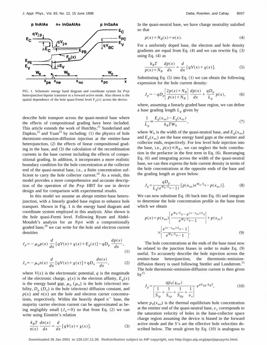
describe hole transport across the quasi-neutral base wthe effects of compositional grading have been includThis article extends the work of Hutchby,21 Sunderland andDapkus,22 and Yuan23 by including: ~1! the physics of holethermionic-emission-diffusion injection at the emitter-baheterojunction,~2! the effects of linear compositional grading in the base, and~3! the calculation of the recombinatiocurrents in the base current including the effects of comsitional grading. In addition, it incorporates a more realisboundary condition for the hole concentration at the collecend of the quasi-neutral base, i.e., a finite concentrationficient to carry the hole collector current.24 As a result, thismodel provides a more comprehensive and accurate destion of the operation of thePnp HBT for use in devicedesign and for comparison with experimental results.
In this model we assume an abrupt emitter-base hetjunction, with a linearly graded base region to enhance htransport. Shown in Fig. 1 is the energy band diagramcoordinate system employed in this analysis. Also showthe hole quasi-Fermi level. Following Ryum and AbdeMotaleb’s analysis for anNpn with a compositionallygraded base,18 we can write for the hole and electron curredensities
Jp52mpp~x!d
dx@qV~x!1x~x!1Eg~x!#2qDp
dp~x!
dx,
~1!
Jn52mnn~x!d
dx@qV~x!1x~x!#1qDn
dn~x!
dx, ~2!
whereV(x) is the electrostatic potential,q is the magnitudeof the electronic charge,x(x) is the electron affinity,Eg(x)is the energy band gap,mp (mn) is the hole~electron! mo-bility, Dp (Dn) is the hole~electron! diffusion constant, andp(x) and n(x) are the hole and electron carrier concenttions, respectively. Within the heavily dopedn1 base, themajority carrier electron current can be approximated asing negligibly small (Jn50) so that from Eq.~2! we canwrite using Einstein’s relation
kBT
n~x!
dn~x!
dx5
d
dx@qV~x!1x~x!#. ~3!
FIG. 1. Schematic energy band diagram and coordinate system forPnpheterojunction bipolar transistor in a forward active mode. Also shown isspatial dependence of the hole quasi-Fermi levelFp(x) across the device.
Downloaded 26 Jan 2001 to 129.137.11.39. Redistribution subject to
ere.
-
rf-
ip-
o-ledis
-
e-
In the quasi-neutral base, we have charge neutrality satisso that
p~x!1NB~x!5n~x!. ~4!
For a uniformly doped base, the electron and hole dengradients are equal from Eq.~4! and we can rewrite Eq.~3!using Eq.~4! as
kBT
p~x!1NB
dp~x!
dx5
d
dx@qV~x!1x~x!#. ~5!
Substituting Eq.~5! into Eq. ~1! we can obtain the followingexpression for the hole current density:
Jp52qDpF2p~x!1NB
p~x!1NBG dp~x!
dx1
qDp
Lgp~x!, ~6!
where, assuming a linearly graded base region, we can dea base grading lengthLg given by
1
Lg[
Eg~xne!2Eg~xnc!
kBTWb, ~7!
whereWb is the width of the quasi-neutral base, andEg(xne)andEg(xnc) are the base energy band gaps at the emittercollector ends, respectively. For low level hole injection inthe base, i.e.,p(x)!NB , we can neglect the hole contribution in the prefactor in the first term in Eq.~6!. RearrangingEq. ~6! and integrating across the width of the quasi-neubase, we can then express the hole current density in termthe hole concentrations at the opposite ends of the basethe grading length as given below
Jp5qDp
Lg~eWb /Lg21!@p~xne!e
Wb /Lg2p~xnc!#. ~8!
We can now substitute Eq.~8! back into Eq.~6! and integrateto determine the hole concentration profile in the base frwhich we obtain
p~x!5p~xne!FeWb /Lg2e~x2xne!/Lg
eWb /Lg21 G1p~xnc!
3Fe~x2xne!/Lg21
eWb /Lg21 G . ~9!
The hole concentrations at the ends of the base mustbe related to the junction biases in order to make Eq.~9!useful. To accurately describe the hole injection acrossemitter-base heterojunction, the thermionic-emissiodiffusion theory is used following Stettler and Lundstrom15
The hole thermionic-emission-diffusion current is then givby15
Jp5qp0~xne!
H 1
Sip1
1
Sep1
1
Sdp1
1
vsJ eqVEB /kBT, ~10!
wherep0(xne) is the thermal equilibrium hole concentratioat the emitter end of the quasi-neutral base,vs corresponds tothe saturation velocity of holes in the base-collector spcharge region assuming the device is biased in the forwactive mode and theS’s are the effective hole velocities described below. The result given by Eq.~10! is analogous to
e
AIP copyright, see http://ojps.aip.org/japo/japcpyrts.html.

i-an
ce
g
bay
thena
der
it
veon
r
th
tae
olth
th
n
er
c-.
terrmi-im-he
nant
ntor
edtheing
n
n
8038 J. Appl. Phys., Vol. 83, No. 12, 15 June 1998 Datta, Roenker, and Cahay
that derived for electron injection across anN2p hetero-junction by Stettler and Lundstrom.15 For the electron injec-tion case, the thermionic emission velocitySin is normallythe smallest and so controls the electron current densityjected into the base.15–19 However, for the case of hole injection in Pnp HBTs considered here, the situation is notclear. We first define the effective hole velocities below athen compare their magnitudes.
Thermionic-field-emission of holes across the valenband spike, including tunneling effects, gives rise to thefective hole interface velocitySip given by
Sip5ghvhe2~DEV2qVjn!/kBT, ~11!
where gh is the hole tunneling factor calculated followinGrinberget al.,16 DEv is the valence band discontinuity,Vjn
gives the band bending on the base side of the emitter-heterojunction andvh is the mean thermal hole velocitgiven byvh[A(kBT)/(2pmh* ), wheremn* is the hole den-sity of states effective mass in the base. In deriving Eq.~11!,since the hole effective mass is very nearly the same inemitter and the base for the InP-based materials, the valband densities of states in the emitter and base are neequal and their difference has been neglected.
The second effective velocity in Eq.~10! is the holedrift-diffusion velocity in the emitter space charge regionSep
given by
Sep5mhE~xj2!e2~DEV2qVjn!/kBT, ~12!
wheremh is the low field hole mobility in the emitter anE(xj
2) is the magnitude of the electric field on the emittside of the heterojunction interface. The third velocitySdp
corresponds to the effective hole velocity associated wdrift diffusion across the quasi-neutral base region, whichdependent on the extent of base grading and is given by
Sdp5vse
Wb /Lg
@11vsLg /Dp~eWb /Lg21!#. ~13!
From ~10! it is apparent that the smallest of the effectihole velocities determines the hole thermionic-emissidiffusion currentJp . To illustrate this, shown in Fig. 2 is aplot of the four-hole velocities as a function of the emittebase bias for the device structure of Stanchinaet al.8 wherethere is no compositional grading in the base. In Fig. 2hole saturation velocityvs (4.53106 cm/s) assumed issomewhat smaller than that for electrons (107 cm s),12 butmuch larger than the other velocities and so is less imporin determining the hole injection current. Similarly, for thcase considered here~no compositional grading!, the holediffusion velocitySdp is larger than eitherSip or Sep so thathole diffusion across the base is limited by the extent of hinjection across the emitter-base junction. As a result,remaining two-hole velocitiesSip or Sep in Eq. ~10! largelydetermine the hole current density. Shown in Fig. 2 isthermionic-emission velocitySip with and without inclusionof the hole tunneling factorgh . The effect of hole tunnelingis to enable additional hole injection across the heterojution so that it effectively raises the velocitySip . The effect issignificant; tunneling increasesSip by more than a factor 10at low bias, but decreases to approximately a factor of 2
Downloaded 26 Jan 2001 to 129.137.11.39. Redistribution subject to
n-
sd
ef-
se
ecerly
his
-
-
e
nt
ee
e
c-
at
high bias. For holes, the low field mobility is much smallthan that for electrons so the velocity prefactor in Eq.~12!makes Sep smaller and comparable to the thermioniemission velocitySip including tunneling as seen in Fig. 2As a result, the drift diffusion of holes across the emitspace charge region is comparable in importance to theonic emission across the valence band discontinuity in liting the hole injection into the base. This is in contrast to tcase for electron injection into the base inNpn HBTs wherethe velocity Sin is the smallest and thermionic emissioacross the conduction band discontinuity is the dominlimiting process.16
Shown in Fig. 3 is the effect of compositional grading othe effective hole velocities calculated at a fixed colleccurrent density of 104 A/cm2. For the effective hole velocitySdp describing drift diffusion across the neutral base definin Eq. ~13!, the velocity rises and then saturates sincequasi-electric field generated by the compositional grad
FIG. 2. Effective hole velocities@emitter space charge region drift diffusio~j!, thermionic emission without~s! and with~d! tunneling, quasi-neutralbase diffusion~m! and base-collector saturation velocity~l!# for InAlAs/InGaAsPnp HBT as a function of emitter-base biasVEB for the case of nocompositional base grading.
FIG. 3. Effective hole velocities@emitter space charge region drift diffusio~j!, thermionic emission without~s! and with~d! tunneling, quasi-neutralbase diffusion~m! and base-collector saturation velocity~l!# in InAlAs/InGaAsPnp as a function of compositional grading (Wb /Lg) in the base.
AIP copyright, see http://ojps.aip.org/japo/japcpyrts.html.

itnginc
inas
owdi
e
nst
th
to
si-seheet
e
n
-ion
th
c-
q.esi-
en-
n.is
u-outby
urem-
ionng
c-cetheles
le
xed
8039J. Appl. Phys., Vol. 83, No. 12, 15 June 1998 Datta, Roenker, and Cahay
aids the hole transport across the base. The hole velocSip andSep are also a function of the compositional gradiin the base and show a steady increase with larger gradThe origin of this effect can be understood as follows. Sinthe emitter energy band gap is fixed~1.47 eV for latticematched InAlAs!, as the extent of compositional gradingthe base increases, the valence band discontinuity decreand the emitter-base junction built-in potential increasesthat the thermionic emission velocitySip given by Eq.~11!and the emitter drift-diffusion velocitySep given by Eq.~12!increase. However, they both remain less thanSdp and sotheir processes continue to control the hole current flacross the emitter-base heterojunction until the base grabecomes large (Wb /Lg.15).
Before matching the hole drift-diffusion current in thbase given by Eq.~8! with the thermionic-emission-diffusioncurrent given by Eq.~10! to determine the hole concentratioat the emitter end of the quasi-neutral base, we follow Da24
and impose the constraint that the hole concentration atcollector end of the base be at least sufficient to carryhole current, i.e.,
p~xnc!5Jp
qvs, ~14!
wherevs is the hole saturation velocity in the base-collecspace charge region. Neglected in Eq.~14! is the effect of thebase-collector biasVCB so that Eq.~14! is not accurate forthe device operating in the forward saturation mode. Subtuting Eq. ~14! into Eq. ~8! and rearranging we get a modfied result for the hole drift-diffusion current in the bawhich is only a function of the hole concentration at temitter end of the base and the device structure paramand is given by
Jp5qvse
Wb /Lg
11~vsLg /Dp!~eWb /Lg21!p~xne!5qSdpp~xne!.
~15!
Equation~15! is the origin of the definition of the effectivehole velocity Sdp associated with drift-diffusion across thbase given previously by Eq.~13!. In the limit of weak com-positional grading (Wb!Lg), the hole current density giveby Eq. ~15! goes to the expected limitq(Dp /Wb)p(xne),while for strong compositional grading (Wb@Lg), the holecurrent becomesq(Dp /Lg)p(xne).
The hole profile in the base given by Eq.~9! can now berewritten by removing the explicit dependence onp(xnc)using Eq.~14! to give
p~x!5p~xne!SdpLg
DpF12S 12
Dp
vsLgDe~x2xnc!/LgG . ~16!
Following Grinberget al.,16 but using the more comprehensive expression for the hole thermionic-emission-diffuscurrent following Stettler and Lundstrom,15 we then set thedrift-diffusion current in the base given by Eq.~15! equal tothe thermionic-emission-diffusion current given by Eq.~10!to determine the hole concentration at the emitter end ofquasi-neutral basep(xne)
Downloaded 26 Jan 2001 to 129.137.11.39. Redistribution subject to
ies
g.e
seso
ng
hee
r
ti-
ers
e
p~xne!5p0~xne!SP
SdpeqVEB /kBT, ~17!
whereSP is defined to be the combination of the hole effetive velocities given by
1
SP5
1
Sip1
1
Sep1
1
Sdp1
1
vs. ~18!
Analogous to Eq.~10!, the size ofSP is largely determinedby the smallest of the effective velocities. As expected, E~17! reduces to the familiar law of the junction when wconsider the homojunction case with diffusion in the quaneutral base as the limiting process.
We can also get a final expression for the hole conctration at the collector end of the quasi-neutral basep(xnc)by combining Eqs.~14! and~15! and then inserting Eq.~17!to give
p~xnc!5Sdp
vsp~xne!5
p0~xne!SP
vseqVEB /kBT. ~19!
SinceSdp is typically less thanvs , p(xnc) will be less thanp(xne) as we expect for typical bipolar transistor operatioHowever, as seen in Fig. 3, when compositional gradingeven moderately large (Wb /Lg.2), we can haveSdp largerthan vs so that from Eq.~19! we see thatp(xnc) can begreater thanp(xne). This corresponds to a dynamic accumlation of holes at the collector end of the base brought abby the efficient transport of holes across the base aidedthe quasi-field created by the compositional grading. Fig3 also indicates that hole injection into the base is still liited by the combination of thermionic-field-emission (Sip)and hole drift diffusion in the emitter space charge reg(Sep). As a result, for a significant range of base gradi(2,Wb /Lg,15), thePnp HBT operates with hole injec-tion into the base limited by a combination of thermionifield-emission and hole drift-diffusion in the emitter spacharge region and a dynamic accumulation of holes atcollector end of the base limited by the transport of hoacross the base-collector space charge region.
To illustrate these results, shown in Fig. 4 is the ho
FIG. 4. Hole concentration profile across the quasi-neutral base for a fiemitter-base bias of 0.8 V for compositional gradings ofWb /Lg50 ~s!, 8~h!, and 12~L!.
AIP copyright, see http://ojps.aip.org/japo/japcpyrts.html.

oittngle
rilvthn
erth
nghea
bangodieaic
wi
th
th
du
ntb
tein-
na
fo
ro
ic
set
es
sa
rge
c-erterng
isheon
he
ec--n-
in
d
8040 J. Appl. Phys., Vol. 83, No. 12, 15 June 1998 Datta, Roenker, and Cahay
profile across the base for several different base comptional gradings where we have assumed a constant embase bias of 0.8 V. For weak compositional gradi(Wb /Lg!1), the hole profile is the normal decreasing hoconcentration since the hole diffusion process is primaresponsible for carrier transport across the base. Howedue to our requirement that the hole concentration atcollector end of the base be sufficient to carry the currei.e., Eq.~14!, the concentration gradient is not large and this a significant hole concentration at the collector end ofbase. For a moderate compositional grading (Wb /Lg58),the hole profile is nearly flat since the quasi-field arisifrom the compositional grading is effective in sweeping tcarriers across the base. As can be seen, the quasi-fieldcauses the hole concentration at the emitter end of thep(xne) to be smaller. For stronger compositional gradi(Wb /Lg.13), the hole profile is nearly flat across mostthe base, but shows an accumulation at the collector enthe base. As described above, this is due to the effictransport of holes across the base as a result of diffusiondrift in the quasi-electric field. The extent of this dynamaccumulation of holes at the collector end of the basealso be a function of the base width as seen from Eq.~19!wherep(xnc) is seen to be proportional toSdp which is givenby Eq.~13!. That is, for a fixed energy gap grading acrossbase, an increase in the base width will reduceDp /Lg andcorrespondingly reduceSdp which will decreasep(xnc) andthe dynamic accumulation of holes at the collector end ofbase.
III. TERMINAL CURRENTS AND CURRENT GAIN
Using the above described results, we can proceedetermine the device’s terminal currents. For the emitter crent, the electron current density due to back injection ithe emitter must be added to the hole component givenEq. ~10!. Similar to the above analysis for holes, the emitthermionic emission electron current density following Grberget al.16,17 is given by
Jne52qveNCBS n~xj2!
NCE2
n~xj1!
NCBe2DEC /kBTD , ~20!
wheren(xj2) and n(xj
1) are the electron concentrations othe emitter and base sides, respectively, of the emitter-bjunction immediately adjacent to the heterojunction atxj ,NCE and NCB are the conduction band density of statesthe emitter and base regions, respectively, andDEC is theconduction band discontinuity. The mean thermal electvelocity ve in Eq. ~20! is given by ve[A(kBT)/(2pme* ),whereme* is the electron density of states effective massthe base. Since the electron effective mass is almost a faof two larger in the emitter than in the base for the InP-bamaterial system,NCE andNCB are not equal and we cannoneglect this difference as we did previously for the holThen, relating the electron concentrations on either sidethe heterojunction to their respective values at the edgethe emitter-base space charge region using the Boltzmrelation, we get
Downloaded 26 Jan 2001 to 129.137.11.39. Redistribution subject to
si-er-
yer,et,ee
lsose
fofntnd
ll
e
e
tor-oy
r
se
r
n
ntord
.ofofnn
n~xj2!5n~xpe!e
qVjp /kBT and n~xj1!5n~xne!e
2qVjn /kBT.~21!
We can then rewrite Eq.~20! as
Jne5qSin@n0~xpe!~eqVEB /kBT21!2Dn~xpe!#, ~22!
whereDn(xpe) is the excess andn0(xpe) is the thermal equi-librium electron concentration at the end of the space charegion in the emitter andSin is the electron heterojunctioninterface velocity defined as
Sin5ve
NCB
NCEeqVjp /kBT
've
NCB
NCES NENB
nie2 De2DEC /kBTe2qVEB /kBT, ~23!
whereNE and NB are the emitter and base doping, respetively, nie is the intrinsic carrier concentration in the emittandVEB is the applied emitter-base junction bias. The latapproximation in Eq.~23! arises because the band bendion the emitter sideVjp can be approximated byVbi2VEB,where NB@NE , where Vbi is the base-emitter junctionbuilt-in potential
Vbi5DEV2DEC
2q1
kBT
qlnS NENB
nienibD
52DEC
q1
kBT
qlnS NENB
nie2 D . ~24!
The electron minority carrier profile in the emittergiven by the usual diffusion profile so that on matching tthermionic emission and diffusion currents, the electrcomponent of the emitter current density is given by19
Jne5qSdnen0~xpe!
11~Sdne/Sin!coth~We /Lne!~eqVEB /kBT21!, ~25!
where we have taken into account the finite width of temitterWe . In Eq.~25! Sdne is the electron diffusion velocityin the emitter given byDne /Lne , whereDne andLne are theelectron diffusion constant and length in the emitter, resptively, andn0(xpe) is the thermal equilibrium electron concentration in the bulk emitter. The total emitter current desity is then given by
Je5Jp1Jne
5qp0~xne!SPeqVEB /kBT
1qSdnen0~xpe!
11~Sdne/Sin!coth~We /Lne!~eqVEB /kBT21!.
~26!
For the collector current, since we have a simplep-nhomojunction, the electron current density for the devicethe normal, forward active mode is given by
Jnc5qDnc
Lncn0~xnc!cothS Wc
LncD , ~27!
whereDnc and Lnc are the electron diffusion constant anlength in the collector, respectively,n0(xnc) is the thermal
AIP copyright, see http://ojps.aip.org/japo/japcpyrts.html.

ndalsitq.
reto
n
n,ttel
na
mio
-peces
-id
ge
eta
i
ieen
d
da-in
ndkenef-ion is
or
o-the
t-
cur-
-
-oreacethe
8041J. Appl. Phys., Vol. 83, No. 12, 15 June 1998 Datta, Roenker, and Cahay
equilibrium electron concentration in the bulk collector aWc is the width of the neutral collector region. The totcollector current is then the sum of the hole current dengiven in Eq.~10! and the electron component given in E~27! so
Jc5Jp1Jnc5qSPp0~xne!eqVEB /kBT
1qDnc
Lncn0~xnc!cothS Wc
LncD . ~28!
Neglecting the recombination currents, the base curis given by the difference of the total emitter and colleccurrents so that on substituting Eqs.~26! and~28! we obtain
Jb5Jne2Jnc
5qSdnen0~xpe!
11~Sdne/Sin!coth~We /Lne!
3~eqVEB /kBT21!2qDnc
Lncn0~xnc!cothS Wc
LncD . ~29!
From the terminal current expressions for the collector athe base currents given in Eqs.~27! and ~28! we can obtainan expression for the small signal current gain
b5p0~xne!
n0~xpe!
SP
SdneF11
Sdne
SincothS We
LneD G . ~30!
In the limit of a homojunction for the emitter-base junctiono compositional grading in the base and no finite emiwidth effect,Sp→Sdp5Dp /Wb and b reduces to the usuaresult.
What is neglected in the expressions for the termicurrent densities given in Eqs.~26!, ~28!, and ~29! are thecontributions, particularly to the base current, of the recobination current components. Inclusion of the recombinatcurrents gives18,19,25
Je5Jp1Jne1Jscr1Jsr1Jire1Jirb1Jbr1Jrr ,
Jc5Jp1Jnc , ~31!
Jb5Jne2Jnc1Jscr1Jsr1Jire1Jirb1Jbr1Jrr ,
whereJrr andJbr are the radiative and nonradiative recombination current densities in the quasi-neutral base, restively, Jsr is the recombination current density at the surfaJscr is the recombination current density in the emitter-baspace charge region, andJirb and Jire are the interface recombination current densities on the base and emitter srespectively, of the emitter-base heterojunction. While Aurecombination is not explicitly included in Eq.~31!, the ef-fects of the base doping on the hole minority carrier lifetimin the base are included based on a fit to experimental dathat the effects of Auger recombination are incorporatedthe nonradiative base recombination currentJbr . Since com-positional grading in the base modifies the minority carrhole profile in the base, the base recombination componare reexamined here.
The nonradiative base recombination current can bescribed starting from19,25
Downloaded 26 Jan 2001 to 129.137.11.39. Redistribution subject to
y
ntr
d
r
l
-n
c-,e
e,r
son
rts
e-
Jbr5qExne
xnc @p~x!2p0~x!#
tpdx, ~32!
wheretp is the minority carrier hole lifetime in the base anp0(x) is the thermal equilibrium minority carrier concentrtion at x, which varies due to the compositional gradingthe base and is given by
p0~x!5ni
2~x!
NB5
NCBNVB
NBe2Eg~x!/kBT. ~33!
Here NCB and NVB are the conduction and valence badensities of states, respectively, in the base which are tato be constant by neglecting the variation in the carrierfective masses across the base. Since the base compositlinearly graded,Eg(x) can be written as
Eg~x!5Eg~xnc!2kBT~x2xnc!
Lg~34!
and on substituting Eqs.~33! and~34! in ~32! and integratingusing Eq.~16! for p(x) we get
Jbr5qLgWbSP
DptpF12
Lg
WbS 12
Dp
vsLgD ~12e2Wb /Lg!G
3p0~xne!eqVEB /kBT2
qni02 Lg
tpNB~12e2Wb /Lg!, ~35!
whereni0 is the intrinsic carrier concentration at the collectend of the base given by
ni02 5NCBNVBe2Eg~xnc!/kBT. ~36!
Similarly, there is also a radiative recombination compnent to the base current. Following our above analysis fornonradiative component we get25
Jrr 5qBNBExne
xncFp~x!2ni
2~x!
NBGdx, ~37!
whereB is the radiative recombination coefficient. Substituing from Eqs.~33! and ~34! and integrating using Eq.~16!for p(x) we get
Jrr 5qBNBLgWbSP
DPF12
Lg
WbS 12
Dp
vsLgD ~12e2Wb /Lg!G
3p0~xne!eqVEB /kBT2qni0
2 LgB~12e2Wb /Lg!. ~38!
The emitter-base space charge region recombinationrent Jscr can also be found starting from19,25
Jscr512 qNtrsveW0An~xne!p~xne!, ~39!
wheres is the carrier capture cross section,Ntr is the recom-bination trap density,ve is the electron thermal velocity defined earlier, andW0 is the fraction of the width of theemitter-base space charge regionWscr in which recombina-tion perdominately occurs and is given by
W05WscrF pkBT
q~Vbi2VEB!G , ~40!
whereVbi andVEB are the emitter-base junction built-in potential and applied bias, respectively. Since the base is mstrongly doped than the emitter, the penetration of the spcharge region into the base is negligibly small so that
AIP copyright, see http://ojps.aip.org/japo/japcpyrts.html.

os.
te
ph
de
onain
uFosth
ra
bi-for
-cur-size.o-oreuc-asedia-
om-ing
mit-s
fec-
aseon thes theEq.
tron
faceer-en-on-
entt ofoesofis-oes
i-
8042 J. Appl. Phys., Vol. 83, No. 12, 15 June 1998 Datta, Roenker, and Cahay
effects of compositional grading have been neglected intaining Eq. ~39! and the following recombination currentSubstituting from Eqs.~33! and ~17! for the carrier concen-trations and simplifying we get
Jscr51
2qNtrsveW0ni0e2Wb/2LgASP
SdpeqVBE/2kBT. ~41!
Similarly, the surface recombination current can be writas19,25
Jsr5qs0Ls
PE
AEni0e2Wb/2LgASP
SdpeqVBE/2kBT, ~42!
wherePE(AE) is the emitter mesa perimeter~area!, s0 is thesurface recombination velocity, andLs is the surface diffu-sion length. Finally, there are additional base current comnents associated with recombination at the emitter-baseerojunction interface, i.e.,Jire and Jirb associated withrecombination at the interface on the emitter and base sirespectively, that are given by19,25
Jire5qsep0~xpe!e2qVbip/kBTF SP
SdpeqVBE /kBT21G ,
Jirb5qsbp0~xne!eqVbin /kBTF SP
SdpeqVBE /kBT21G , ~43!
wherese andsb are the interface recombination velocitiesthe emitter and base sides heterojunction, respectively,Vbin and Vbip are the fractions of the emitter-base built-potential on the emitter and base sides, respectively.
Utilizing the above results, we can examine the variocontributions to the base current. These are displayed in5 as a function of compositional grading at a constant clector current density of 104 A/cm2. The material parameterused in the calculations are summarized in Table I anddevice structure is similar to that of Stanchinaet al.8,9 Theresults show that in the absence of compositional base g
FIG. 5. Base recombination currents@nonradiativeJbr ~s! and radiativeJrr
~h!, space charge regionJscr ~L!, surfaceJsr ~n!, emitter side interfaceJire ~l!, base side interfaceJirb (x)#, electron back injectionJne ~m!,electron collector leakageJnc ~d! and total base current~no symbol! as afunction of compositional base grading (Wb /Lg).
Downloaded 26 Jan 2001 to 129.137.11.39. Redistribution subject to
b-
n
o-et-
s,
nd
sig.l-
e
d-
ing, the base current is dominated by nonradiative recomnation in the quasi-neutral base region as frequently seenInP-basedNpn HBTs. As the extent of compositional grading in the base increases, the nonradiative recombinationrent as well as most of the other components decrease inThis effect results from the fact that with increased compsitional grading, the quasi-electric field is enhanced and meffectively sweeps holes out of the quasi-neutral base reding the hole concentration across the entire width of the bas seen in Fig. 4. This effect reduces not only the nonrative and radiative components as expected Eqs.~35! and~38!, but also the interface and space charge region recbination components. The latter results from the increasquasi-field which reduces the hole concentration at the eter end of the basep(xne) as seen in Fig. 4, which reducethe interface recombination current as seen from Eq.~39!.Similarly, the increasing base quasi-field increases the eftive hole diffusion velocity in the baseSdp as seen in Fig. 3,which causes the interface recombination current to decreas seen from Eq.~43!. Finally, the quasi-field in the base alsdrives holes away from the exposed base surface betweeemitter mesa and the base metal contact and so reducebase surface recombination current as seen in Fig. 4 and~42!.
By contrast, the base current component due to elecback injection into the emitterJne given by Eq.~25! risessteadily as the extent of base grading increases. The interrecombination on the emitter side of the heterojunction intface also increases, but remains small. Since the emitterergy band gap is fixed, with increased base grading the cduction band discontinuity is reduced so thatSin given by Eq.~23! is enlarged andJne given by Eq.~25! increases. As aresult, at large enough base grading (Wb /Lg.18), electronback injection into the emitter dominates the base currand the base current begins to increase. The net effecincreasing base grading is that the total base current gthrough a broad minimum. The corresponding effectscompositional grading on the dc current gain for the transtor are seen in Fig. 6. As expected, the current gain g
TABLE I. Material parameters for Pnp InAlAs/InGaAs heterojunction bpolar transistor.
Emitter Base Collector
InAlAs p-type InGaAsn-type InGaAsp-typeEg51.47 eV Eg(xnc)50.75 eV Eg50.75 eVxE54.1 eV xB(xnc)54.58 eV xC54.58 eVNE5131018/cm3 NB5531018/cm3 NC5531016/cm3
We50.14mm Wb50.06mm Wc50.3mmLne53.8mm Lp50.48mm Lnc55.2mmDne514.5 cm2/s Dp52.6 cm2/s Dnc5300 cm2/smh559 cm2/V s mp5100 cm2/V s mn51160 cm2/V s
me* 50.041m0 me* 50.041m0
mpe* 50.48m0 mh* 50.47m0 mh* 50.47m0
nie59.33105/cm3 ni056.531011/cm3
se510 cm/s sb510 cm/stp50.9 ns vs54.53106 cm/s
rec5131026 V cm2 rbc5131027 V cm2 rcc5131026 V cm2
Ntr5431016/cm2 B54.2310211 cm3 ss54310217 cm2 s0Ls5231024 cm2/s
AIP copyright, see http://ojps.aip.org/japo/japcpyrts.html.

gero
re
thc
ee
trer
or
t ofthe
theuce
thencese.he
to
nce
e
cor-.e
n
yd-
ndhe
canom-tive
ity
.
8043J. Appl. Phys., Vol. 83, No. 12, 15 June 1998 Datta, Roenker, and Cahay
through a broad maximum as the base grading is enlarThe enhancing effect of the base grading is significant pducing nearly an order of magnitude increase in the curgain reaching a maximum of 1700 nearWb /Lg515.
IV. BASE TRANSIT TIME AND CUTOFF FREQUENCY
The incorporation of grading in the base also impactsbase transit time and so the high frequency performancepabilities of the device. ForPnp HBTs, the low hole diffu-sion constant in the base makes the hole base transit timdominant component in the emitter-to-collector delay timFollowing Pulfrey20,26and Ferryet al.,27 we can calculate thebase transit time from
tb5Exne
xnc 1
vh~x!dx, ~44!
where vh(x) is the average hole velocity atx in the basewhich is related to the hole current densityJp by
Jp5qvh~x!@p~x!2p0~x!#, ~45!
where the quantity in brackets is the excess hole concention atx. Due to compositional grading in the base, the thmal equilibrium concentrationp0 is also a function ofx andcombining Eqs.~33! and ~34! we can write
p0~x!5ni0
2
NBe~x2xnc!/Lg, ~46!
whereni0 is the intrinsic carrier concentration at the collectend of the quasi-neutral base. Solving Eq.~45! for vh(x) andsubstituting into Eq.~44!, we can integrate Eq.~44! usingEq. ~16! for p(x) and Eq.~46! for p0(x) to obtain
tb5Wb
2
2DpH 2Lg
WbF12
Lg
WbS 12
Dp
vsLgD ~12e2Wb /Lg!G J
2ni0
2 Lge2qVEB /kBT
SPNBp0~xne!~12e2Wb /Lg!, ~47!
where we have used Eqs.~15! and~17! to simplify the result.The last term in Eq.~47! arises from the variation in the
FIG. 6. DC current gain~s! as a function of base grading (Wb /Lg) includ-ing base recombination current components for a collector current dens104 A/cm2.
Downloaded 26 Jan 2001 to 129.137.11.39. Redistribution subject to
d.-
nt
ea-
a.
a--
intrinsic concentration across the base region. In the limino compositional grading in the base, this reduces tousual resultWb
2/2Dp1Wb /Vs .24 However, when composi-tional grading is used, the quasi-field in the base aidshole transport across the base and can significantly redthe base transit time as shown below.
Not included in the present model are the effects onbase transit time of hot hole injection across the valeband discontinuity and ballistic transport across the baThe present model includes only drift diffusion across tbase of thermalized holes. ForNpn HBTs, the effects of hotelectron injection and ballistic transport have been shownimpact the base transit time for InP-based devices.28 Due tothe small base widths, e.g., 35 nm, and the large valeband discontinuities~0.24 and 0.34 eV for InAlAs/InGaAsand InP/InGaAs, respectively!, similar effects may also beimportant for thePnp HBTs. There have also been somprevious reports of ballistic hole transport.29–31Further studyis needed to examine the extent of these effects and to inporate the effects in the analysis of the base transit time
The cutoff frequency for the HBT is determined by thtotal emitter-to-collector delay timetec given by32
tec5kBT
qIC$Cbe1Cbc%1tb1tbc1$Re1Rc%Cbc , ~48!
where Cbe and Cbc are the emitter and collector junctiodepletion capacitances, respectively,Re andRc are the emit-ter and collector series resistances,I c is the dc collector cur-rent and tbc is the base-collector delay time given bWbc/2vs . The emitter and collector resistances were moeled following Ho and Pulfrey20 using the parameters givein Table I, whererec , rbc , andrcc are the emitter, base, ancollector contact resistivities. Seen in Fig. 7 is a plot of ttransit time components and thetec as a function of thecollector current density for the device of Stanchinaet al.8
for the case of no compositional grading in the base. Asbe seen, the base transit time is one of two dominant cponents so that use of compositional grading can be effecin reducing the totaltec and improving the cutoff frequency
ofFIG. 7. Transit time components@base transit timetb ~s!, emitter chargingtime te ~d!, collector delay timetbc ~h! and collector charging timetc
~n!# and total emitter-to-collector delay timetec ~no symbol! versus collec-tor current density in the case of no compositional grading in the base
AIP copyright, see http://ojps.aip.org/japo/japcpyrts.html.

hee
pt
sere
e
hena
e
d
a-
ig-thilexi-of
xedalop-
y o
ing
8044 J. Appl. Phys., Vol. 83, No. 12, 15 June 1998 Datta, Roenker, and Cahay
of the device. As an illustration, seen in Fig. 8 is a plot of tbase transit time using Eq.~47! as a function of the basgrading at a fixed collector current density of 104 A/cm2. Forcomparison, also shown are the other transit time comnents, which are independent of the base grading, andtotal emitter-to-collector transit time. The effects of bagrading ontb are dramatic producing a reduction of mothan an order of magnitude. However, beyond a gradingWb /Lg58, there is little benefit on device speed of increasgrading as the collector delay time dominates thetec .
Figure 9 is a plot of the cutoff frequency versus tcollector current density for a series of three compositiogradings in the base region (Wb /Lg50, 8, and 24!. Clearly,the cutoff frequency is significantly enhanced~by more than50%! when the compositional grading is employed (Wb /Lg
58). However, there is only a modest additional improvment when the grading is increased fromWb /Lg58 to 24, asexpected from Fig. 8.
Seen in Fig. 10 are the cutoff frequencyf T and maxi-
FIG. 8. Transit time components@base transit timetb ~s!, emitter chargingtime te ~d!, collector delay timetbc ~h! and collector charging timetc
~n!# and total emitter-to-collector delay timetec ~no symbol! as a functionof the compositional grading in the base for a collector current densit104 A/cm2.
FIG. 9. Cutoff frequency forWb /Lg50 ~s!, 8 ~h!, and 24~L! and maxi-mum frequency of oscillation forWb /Lg50 ~d!, 8 ~j!, and 24~l! vscollector current density.
Downloaded 26 Jan 2001 to 129.137.11.39. Redistribution subject to
o-he
ofd
l
-
mum frequency of oscillationf max for a collector currentdensity of 104 A/cm2 as a function of base width for a fixebase doping of 731018/cm3 for no compositional gradingand a grading ofWb /Lg524. The f max was calculated fromthe f T using
f max5A f T
8p~RBCC!eff, ~49!
where (RBCC)eff is the effective base resistance-collector cpacitance product defined by Ho and Pulfrey.20 For both thef T and f max frequencies, the effects of base grading are snificant, particularly for larger base widths. At a base widof 50 nm, the cutoff frequency is more than doubled whthe maximum frequency of oscillation increases by appromately 30%. Similarly, seen in Fig. 11 are the effectscompositional grading (Wb /Lg524) versus no grading onthe two frequencies as the base doping is varied for a fibase width of 33 nm. Again, the effects of compositionbase grading are significant, particularly at the highest d
f
FIG. 10. Cutoff frequency without~s! and with base grading~d! andmaximum frequency of oscillation without~h! and with base grading~j! asa function of base width for a fixed base doping of 731018/cm3 for a basegrading ofWb /Lg524 for a collector current density of 104 A/cm2.
FIG. 11. Cutoff frequency without~s! and with base grading~d! andmaximum frequency of oscillation without~h! and with base grading~j! asa function of base doping for a fixed base width of 33 nm for a base gradof Wb /Lg524 for a collector current density of 104 A/cm2.
AIP copyright, see http://ojps.aip.org/japo/japcpyrts.html.
xel
fon-anine
erb
eten
sjeoncasxi
hen
ente
o
icafoinlinr
ritaer
thb
un
y
e
K.tt.
c-na-
en,of
ice
na,
ina,hide
w,
e
s.
s
at-
theteri-
F.
theteri-
8045J. Appl. Phys., Vol. 83, No. 12, 15 June 1998 Datta, Roenker, and Cahay
ing levels. At a base doping of 231019/cm3, the cutoff fre-quency is enhanced by approximately 50%, while the mamum frequency of oscillation increases by approximat10%.
V. CONCLUSION
In summary, we have presented an analytical modelthe Pnp HBT that takes into account thermionic-emissiodiffusion of holes across the emitter-base heterojunctionmatches this hole injection with the drift-diffusion currentthe base to determine self-consistently the hole current dsity. The effects of compositional grading of the base walso incorporated in the determination of the base recomnation currents. The results were used to examine the effof base grading on the transistor’s current–voltage characistics and current gain. An optimum base grading was fouwhere the reduction in the base recombination currentsignificant, but the effects of enhanced electron back intion into the emitter not yet dominant. Also, the effectsbase grading on the device’s high frequency performawere analyzed and shown to be effective in reducing btransit time and improving the cutoff frequency and mamum frequency of oscillation.
The feasibility of the use of compositional grading in tbase forNpn InP-based HBTs has recently been demostrated by Kurishimaet al.28 and Ohkuboet al.33 usingstrained In12xGaxAs. Chirped superlattices have also besuccessfully employed to compositionally grade the emitbase and base-collector junction inNpn HBTs.34,35 Furtherstudy is needed of hot hole injection and ballistic transpeffects to determine the optimum base grading for thePnpHBT.
As a final note, the model of tunneling and thermionemission presented in this article assumes an effective mfor carriers equal to the density of states effective massholes. A more thorough investigation should include andependent calculation of the light and heavy hole tunneacross the emitter-base junction. We have used a scattematrix approach to this problem36 and have shown that foInP/In0.53Ga0.47 As heterojunctions, the split-off spin-orbband can have a dramatic influence on the tunneling of heand light holes and on the energy distribution of the carriinjected into the base.37 This in turn will influence the basetransit time and hence the high frequency response ofdevice. Our results will be presented in a forthcoming pulication.
ACKNOWLEDGMENT
This work was supported by the National Science Fodation under Grant No. ECS-9525942.
1J. Bales, IEEE J. Solid-State Circuits32, 1470~1997!.2D. B. Slater, P. M. Enquist, F. E. Najjar, M. Y. Chen, and J. A. HutchbIEEE Electron Device Lett.11, 146 ~1990!.
3H. Q. Tserng, D. G. Hill, and T. S. Kim, IEEE Microwave Guid. WavLett. 3, 45 ~1993!.
Downloaded 26 Jan 2001 to 129.137.11.39. Redistribution subject to
i-y
r
d
n-ei-
ctsr-disc-fee
-
-
r-
rt
ssr
-ging
vys
e-
-
,
4D. G. Hill, T. S. Kim, and H. Q. Tserng, IEEE Electron Device Lett.14,185 ~1993!.
5G. J. Sullivan, M. F. Chang, N. H. Sheng, R. J. Anderson, N. L. Wang,C. Wang, J. A. Higgins, and P. M. Asbeck, IEEE Electron Device Le11, 463 ~1990!.
6W. Liu and C. Dai, Jpn. J. Appl. Phys., Part 231, L452 ~1992!.7G. B. Gao, D. J. Roulston, and H. Morkoc, Solid-State Electron.33, 1209~1990!.
8W. E. Stanchina, R. A. Metzger, M. W. Pierce, J. F. Jensen, L. G. MCray, R. Wong-Quen, and F. Williams, Proceedings of the Fifth Intertional Conference on InP and Related Materials, 1993, p. 569.
9W. E. Stanchina, R. A. Metzger, D. B. Rensch, L. M. Burns, J. F. JensR. H. Walden, L. E. Larson, and P. T. Greiling, GOMAC-91 DigestPapers, 1991, p. 385.
10L. M. Lunardi, S. Chandrasekhar, and R. A. Hamm, IEEE Electron DevLett. 14, 19 ~1993!.
11S. Shi, K. P. Roenker, T. Kumar, M. M. Cahay, and W. E. StanchiIEEE Trans. Electron Devices43, 1466~1996!.
12S. Datta, S. Shi, K. P. Roenker, M. M. Cahay, and W. E. StanchProceedings of the Ninth International Conference on Indium Phospand Related Materials, 1997, p. 392.
13D. B. Slater, P. M. Enquist, J. A. Hutchby, A. S. Morris, and R. J. TreIEEE Electron Device Lett.15, 91 ~1994!.
14W. Liu, D. Hill, D. Costa, and J. S. Harris, IEEE Microwave Guid. WavLett. 2, 331 ~1992!.
15M. A. Stettler and M. S. Lundstrom, IEEE Trans. Electron Devices41,592 ~1994!.
16A. A. Grinberg, M. S. Shur, R. J. Fischer, and H. Morkoc, IEEE TranElectron Devices31, 1758~1984!.
17A. A. Grinberg and S. Luryi, IEEE Trans. Electron Devices40, 859~1993!.
18B. R. Ryum and I. M. Abdel-Motaleb, Solid-State Electron.34, 1125~1991!.
19B. R. Ryum and I. M. Abdel-Motaleb, Solid-State Electron.33, 869~1990!.
20S. C. M. Ho and D. L. Pulfrey, IEEE Trans. Electron Devices36, 2173~1989!.
21J. A. Hutchby, IEEE Electron Device Lett.7, 108 ~1986!.22D. A. Sunderland and P. D. Dapkus, IEEE Trans. Electron Devices34,
367 ~1987!.23J. S. Yuan, Solid-State Electron.34, 1347~1991!.24M. B. Das, in HEMTs and HBTs: Devices, Fabrication and Circuits,
edited by F. Ali and A. Gupta~Artech House, Boston, 1991!, Chap. 4, p.191.
25B. R. Ryum and I. M. Abdel-Motaleb, IEE Proc.-G: Circuits, DeviceSyst.138, 115 ~1991!.
26O. S. Ang and D. L. Pulfrey, Solid-State Electron.34, 1325~1991!.27D. K. Ferry, L. A. Akers, and E. W. Greeneich, inUltra Large Scale
Integrated Microelectronics~Prentice–Hall, Englewood Cliffs, NJ, 1988!,p. 112.
28K. Kurishima, H. Nakajima, S. Yamahata, T. Kobayashi, and Y. Msuoka, Jpn. J. Appl. Phys., Part 134, 1221~1995!.
29S. L. Chuang, Phys. Rev.40, 10379~1989!.30C. Y. P. Chao and S. L. Chuang, Phys. Rev. B43, 7027~1991!.31K. Brennan and K. Hess, Phys. Rev. B29, 5581~1984!.32W. Liu, D. Costa, and J. S. Harris, Solid-State Electron.35, 541 ~1992!.33M. Ohkubo, J. Osabe, N. Ikeda, and T. Ninomiya, Proceedings of
Ninth International Conference on Indium Phosphide and Related Maals, 1997, p. 641.
34H. Hafizi, W. E. Stanchina, R. A. Mtezger, P. A. MacDonald, andWilliams, Jr., IEEE Trans. Electron Devices40, 1583~1993!.
35K. Yang, G. O. Munns, X. Wang, and G. I. Haddad, Proceedings ofNinth International Conference on Indium Phosphide and Related Maals, 1997, p. 645.
36T. Kumar, M. M. Cahay, and K. P. Roenker, Phys. Rev. B56, 4836~1997!.
37S. Ekbote, M. M. Cahay, and K. P. Roenker, Phys. Rev. B~submitted!.
AIP copyright, see http://ojps.aip.org/japo/japcpyrts.html.


