Embed Size (px)
Citation preview
1
A comparing study on optoelectronic properties of phototransistors based
on MEH-PPV and PbS QD hybrids with bulk- and layer-heterojunction
Xiaoxian Song,1, 2
Yating Zhang,1, 2, a)
Ran Wang,1, 2
Mingxuan Cao,1, 2
Yongli Che,1, 2
Jianlong
Wang,1, 2
Haiyan Wang,1, 2
Lufan Jin,1, 2
Haitao Dai,3 Xin Ding,
1, 2 Guizhong Zhang,
1, 2 and
Jianquan Yao1, 2
1Institute of Laser & Opto-Electronics, College of Precision Instruments and Opto-electronics Engineering,
Tianjin University, Tianjin 300072, China
2Key Laboratory of Opto-electronics Information Technology (Tianjin University), Ministry of Education,
Tianjin 300072, China
3Tianjin Key Laboratory of Low Dimensional Materials Physics and Preparing Technology, School of
Science, Tianjin University, Tianjin 300072, China
As the responsivity (R) of a thin film photo detector is proportional to the product of the photo-
induced carrier density (n) and mobility (μ) (Z. Sun, Z. Liu, J. Li, G.-a. Tai, S. Lau and F. Yan, Adv.
Mater., 24, 5878, 2012), which of the types is conducive to photo detection, choosing between layer-
heterojunction (LH) and bulk-heterojunction (BH) field effect phototransistors (FEpTs), is still unknown.
A comparison study is performed based on an MEH-PPV and PbS QDs hybrid. They are both
demonstrated as being ambipolar, with μE≈μH=3.7 cm2V
-1s
-1 for BH-FEpTs and μH=36 cm
2V
-1s
-1, μE=52
cm2V
-1s
-1 for LH-FEpTs. Due to the greatly improved μ and high channel order degree (α), the R of the
LH-FEpTs reaches as high as 101A/W, whereas that of the BH-FEpTs is as low as 10
-1A/W. Although
the large area of the BH improves the exciton separation degree (β) and n, the lack of effective transport
becomes the main constraint on high responsivity. Therefore, LH-FEpTs are a better candidate, and a
“three-high” principle of high α, β, and μ is required for high R values.
_____________________________
a) Author to whom correspondence should be addressed. Electronic mail: [email protected].
2
FEpTs based on a solution-processed polymer, semiconductor quantum dots (QDs) and a hybrid of both have achieved
ultrahigh performances1-6
and are attracting more and more attention due to their great potential for applications in near
infrared (NIR) detectors with low cost, flexibility, easy fabrication and easy integration7-10
. As a center of exciton (electron-
hole pairs) separation, heterojunctions play a critical role in photo detection, which converts photons into an electric current
or voltage11, 12
. Two typical heterojunctions for FEpT channel structures are BH and LH. Photo responses have been reported
for both of them. Yan’s group has reported BH-FEpTs based on a poly (3-hexylthiophene) (P3HT) and lead sulfide quantum
dots (PbS QDs) hybrid. Under a bias of 100 V, NIR photo responsivity reaches as high a 104
A/W13
. Yan’s group and
Konstantato et al. have both reported on LH-FEpTs based on a graphene and PbS colloidal QDs hybrid with ultrahigh
responsivity of 107 A/W
14, 15.
Theoretically, the responsivity Rph of a thin film photoconductor is expressed as Rph = enμEW/P, where e is the
electronic charge, n is the density of photo-induced carriers per unit area, μ is the carrier mobility, E is the applied electric
field, P is the incident optical power, and W is the width of the device15
. Based on these parameters, each type has both
advantages and disadvantages. BH has a larger area of exciton separation (high n) but irregular-shaped channels, where
carriers transport inefficiently (low μ)16
; LH has regular-shaped channels ( high μ), but a small area of exciton separation
(low n) 14, 15
.
However, which type achieves higher responsivity (~n×μ) is still undetermined. Here, both types are fabricated based on
a poly [2-methoxy-5-(20-ethylhexyloxy- p-phenylenevinylene)] (MEH-PPV) and PbS QDs hybrid. Using a comparison
method, the transfer characteristics and the responsivities of the two types are investigated experimentally. Because the
mobility of LH-FEpTs is one order of magnitude larger than that of BH-FEpTs and the channel order degree of LH-FEpTs is
larger than that of BH-FEpTs, the responsivity of LH-FEpTs is of the order of 101 A/W, whereas that of BH-FepTs is ~ 10
-1
A/W. Therefore, an effective carrier transport mechanism is the shortcoming of BH-FEpTs.
3
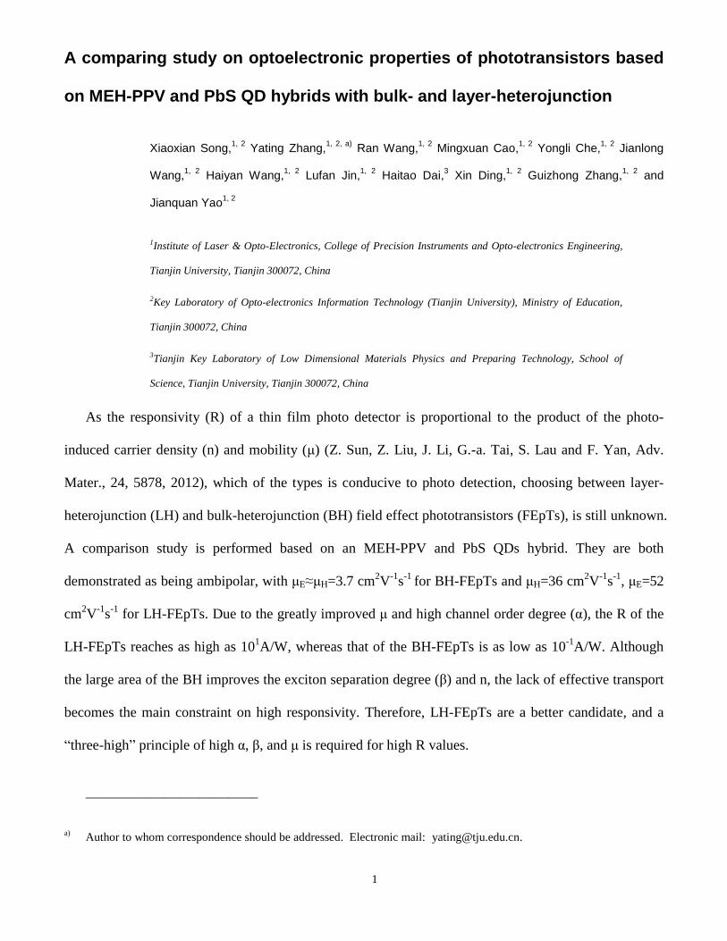
FIG. 1. (a) Absorbance and the PL spectrum of PbS QDs, the insert is TEM image of PbS QDs. (b) FTIR spectra of MEH-PPV, PbS
QDs and their hybrid.
MEH-PPV was purchased from Luminescence Technology Corporation (No. LT-S931). PbS QDs was synthesized via a
wet chemical method17, 18
(for the detailed method, see supplementary material [19]). As shown in Figure 1 (a), optical
characterization of the QDs, including absorption and photoluminescence (PL) spectra, was performed on a PbS QD toluene
solution by using a Zolix Omni-λ300 spectrometer. The absorption peak was located at 1245 nm, while the PL peak was
located at 1420 nm as excited by a 532 nm cw laser from Changchun New Industries Optoelectronics Technology Co., Ltd.
According to a four-band-envelope-function formulism, the average diameter of PbS QDs was calculated as 4.8 nm20
. The
TEM image of the QDs was created using a transmission electron microscope (TEM) from FEI Co., Tecnai G2 F20, with 200
kV. Based on the TEM image, the average size of the PbS QDs was 4.8 nm, exhibiting good consistency with the diameter
deduced from the absorption spectrum shown in Figure 1 (a).
The hybrid solution was prepared by combining one volume of MEH-PPV (5 mg/ml) and three volumes of PbS QDs (10
mg/ml) toluene solution. The transmission peaks of PbS QDs, MEH-PPV, and their hybrid were determined using Fourier
transform infrared (FTIR) spectra (FTIR-650-spectrometer from Tianjin Gangdong sci.&tech. development Co., Ltd.), as
shown in Figure 1 (b). For both PbS QDs and MEH-PPV, FTIR represents the properties of ligand (-OLA) and MEH-PPV,
respectively. For the hybrid, the characteristic peaks are viewed as superpositions of the peaks from the PbS QDs and MEH-
PPV individuals. Please note that there is no exchange between the ligand of PbS QDs and MEH-PPV, which ensures the
consistent heterojunction of the two types.
4
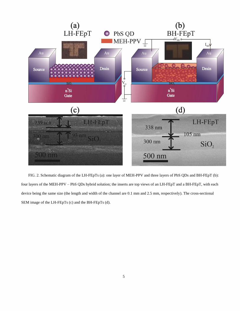
BH-FEpTs and LH-FEpTs based on the MEH-PPV-PbS QDs hybrid were fabricated experimentally18, 19
. The schematic
diagrams of both are displayed in Figure 2 (a) and (b). The substrates used are Si n+/SiO2. The thickness of SiO2 is 300 nm,
on which an Au source and drain with a thickness of 200 nm were thermally evaporated over a shadowed mask.
The layer-heterojunction channel consists of one layer of MEH-PPV and three layers of PbS QDs, as shown in Figure 2
(a). The fabrication procedure was as follows: one drop of MEH-PPV toluene solution (5 mg/ml) was spin-casted on the
substrate at a spin speed of 2000 rpm and left to dry for 15 seconds. Then, three layers of PbS QDs were deposited through a
layer-by-layer film and ligand exchange process. Each layer was prepared as follows: 2% (Vol.) ethanedithiol (EDT) in
acetonitrile solution was first prepared for ligand exchange. The PbS QDs toluene solution was prepared at 10 mg/mL in
toluene. A drop of PbS QD layer was first deposited on the spinning substrate with a speed of 2000 rpm and left for 15
seconds to dry. Three drops of 2% EDT solution were then deposited on the rotating substrate, followed by 2 drops of
acetonitrile and 2 drops of toluene.
The bulk-heterojunction channel was prepared by spin-casting four layers of the hybrid solution. Each layer was
deposited at a spin speed of 2000 rpm and left for 15 seconds to dry. Then, both FEpTs were left in a vacuum overnight
before electric measurement.
The SEM images of cross sections of LH-FEpTs and BH-FEpTs are given by Figure 2 (c) and (d), respectively. The
structure of each device is very clearly visible. The bottom layer is Si n+, on which is SiO2 layer. The thickness is attributed
to 300 nm. The top layer is channel layer. The thickness of such layer in LH-FEpT is 332 nm (including one layer of MEH-
PPV in thickness of 93 nm and three layers of PbS QDs in thickness of 239 nm), and that of BH layer is 337 nm. Clearly,
delamination presented in LH is absent in BH, due to fabrication method.
During the electric measurement, a bias voltage (VSD) was applied over the source (ground connection) and drain
electrodes by using a Keithley 2400; the channel current flowing into the drain was denoted by ISD, which was also detected
using the Keithley 2400. A gate voltage (VG) was applied on the gate electrode to the ground connection by using a
HP6030A, as shown in Figure 2 (b).
5
FIG. 2. Schematic diagram of the LH-FEpTs (a): one layer of MEH-PPV and three layers of PbS QDs and BH-FEpT (b):
four layers of the MEH-PPV – PbS QDs hybrid solution; the inserts are top views of an LH-FEpT and a BH-FEpT, with each
device being the same size (the length and width of the channel are 0.1 mm and 2.5 mm, respectively). The cross-sectional
SEM image of the LH-FEpTs (c) and the BH-FEpTs (d).
6
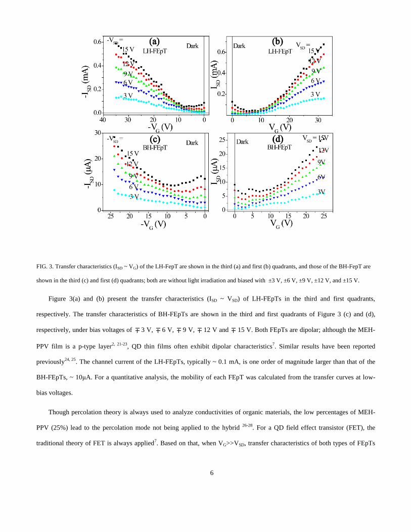
FIG. 3. Transfer characteristics (ISD ~ VG) of the LH-FepT are shown in the third (a) and first (b) quadrants, and those of the BH-FepT are
shown in the third (c) and first (d) quadrants; both are without light irradiation and biased with ±3 V, ±6 V, ±9 V, ±12 V, and ±15 V.
Figure 3(a) and (b) present the transfer characteristics (ISD ~ VSD) of LH-FEpTs in the third and first quadrants,
respectively. The transfer characteristics of BH-FEpTs are shown in the third and first quadrants of Figure 3 (c) and (d),
respectively, under bias voltages of 3 V, 6 V, 9 V, 12 V and 15 V. Both FEpTs are dipolar; although the MEH-
PPV film is a p-type layer2, 21-23
, QD thin films often exhibit dipolar characteristics7. Similar results have been reported
previously24, 25
. The channel current of the LH-FEpTs, typically ~ 0.1 mA, is one order of magnitude larger than that of the
BH-FEpTs, ~ 10μA. For a quantitative analysis, the mobility of each FEpT was calculated from the transfer curves at low-
bias voltages.
Though percolation theory is always used to analyze conductivities of organic materials, the low percentages of MEH-
PPV (25%) lead to the percolation mode not being applied to the hybrid 26-28
. For a QD field effect transistor (FET), the
traditional theory of FET is always applied7. Based on that, when VG>>VSD, transfer characteristics of both types of FEpTs
7
lie in a linear region (ISD VG) due to the constant mobility of holes (in the third quadrant) or electrons (in the first quadrant).
The mobility can be expressed by12, 20
( )
D
ox SD G T
IL
WC V V V
(1)
where W and L are the width and length of the channel, respectively. Cox is the capacitance of the gate dielectric per unit area.
In such a region, ID/(VG - VT) = ΔID/ΔVG. As a result, the slope of ΔID/ΔVG can be obtained by linear fitting on the transfer
characteristic curves at a low-bias voltage, and then, the mobility can be calculated according to equation (1). With VSD = 0.3
V, W = 2.5 mm, L = 0.1 mm, and Cox ~ 100 pF, we determined the mobilities of holes in the third and of electrons in the first
quadrants to be μH = 36 cm2V
-1 s-1 and μE = 52 cm
2V
-1 s-1 for LH-FEpTs. Similarly, we also obtained the mobilities as being μH
= 3.7 cm2V
-1 s-1 and μE = 3.8 cm
2V
-1 s-1 for BH-FEpTs. Therefore, we conclude that the mobility of LH-FepTs is one order of
magnitude higher than that of BH-FEpTs in both the third and first quadrants.
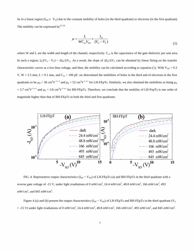
FIG. 4. Representive output characteristics (ISD ~ VSD) of LH-FEpTs (a) and BH-FEpTs in the third quadrant with a
reverse gate voltage of -15 V, under light irradiations of 0 mW/cm2, 24.4 mW/cm
2, 48.8 mW/cm
2, 166 mW/cm
2, 493
mW/cm2, and 845 mW/cm
2.
Figure 4 (a) and (b) present the output characteristics (ISD ~ VSD) of LH-FEpTs and BH-FEpTs in the third quadrant (VG
= -15 V) under light irradiations of 0 mW/cm2, 24.4 mW/cm
2, 48.8 mW/cm
2, 166 mW/cm
2, 493 mW/cm
2, and 845 mW/cm
2.
8
Both types of FEpTs show the decrease of channel current with the increase in light irradiation due to the light-gate effect13, 14,
21.
The physical mechanism of the sensing of light is described as follows. Under light illumination, photo-induced excitons
are generated in the PbS QDs. Under an electric field driving force, excitons are separated into free electrons and holes in the
QDs. Due to the role of gate voltage in driving carriers, holes (or electrons, depending on gate voltage) are transferred from
the upper to the bottom layer where the channel was formed. Meanwhile, electrons (or holes) in equal numbers remain in the
upper layers, which form the electric field in a direction opposite to that of the gate electric field. It was regarded as an
additional photo-induced gate voltage, termed the “light-gate effect.” Due to this effect, horizontal shifts, ΔVG, can be used
with FEpTs to calibrate light irradiance (Ee) as 29
G eV E (2)
where α and β are constant. According to equation (1), the increments in the channel current ΔISD, resulting from
the light illumination, are expressed as a function of the gate shift ΔVG:
SD ox SD G
WI C V V
L
(3)
For one device, oxWC L is constant, and ΔISD is directly proportion to VSDΔVG.
However, ΔVG is hard to measure directly. The responsivity (R) of a FEpT is always defined by ΔISD as30
ill Dark SDI I IR
P P
(4)
where Iill and IDark are the channel current under light illumination and in the dark, respectively, and P =AEe is the incident
optical power, where A is the illumination area. Substituting equation (3) into (4), one gets
1
2 2
ox SD ox SDG e
e
C V C VR V E
L E L
(5a)
2lg(R) lg 1 lg( )ox SD
e
C VE
L
(5b)
9
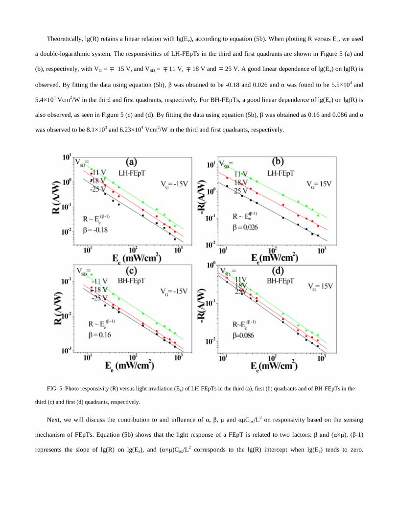
Theoretically, lg(R) retains a linear relation with lg(Ee), according to equation (5b). When plotting R versus Ee, we used
a double-logarithmic system. The responsivities of LH-FEpTs in the third and first quadrants are shown in Figure 5 (a) and
(b), respectively, with VG = 15 V, and VSD = 11 V, 18 V and 25 V. A good linear dependence of lg(Ee) on lg(R) is
observed. By fitting the data using equation (5b), β was obtained to be -0.18 and 0.026 and α was found to be 5.5×10⁴ and
5.4×10⁴ Vcm
2/W in the third and first quadrants, respectively. For BH-FEpTs, a good linear dependence of lg(Ee) on lg(R) is
also observed, as seen in Figure 5 (c) and (d). By fitting the data using equation (5b), β was obtained as 0.16 and 0.086 and α
was observed to be 8.1×10³ and 6.23×10
4 Vcm
2/W in the third and first quadrants, respectively.
FIG. 5. Photo responsivity (R) versus light irradiation (Ee) of LH-FEpTs in the third (a), first (b) quadrants and of BH-FEpTs in the
third (c) and first (d) quadrants, respectively.
Next, we will discuss the contribution to and influence of α, β, μ and αμCox/L2 on responsivity based on the sensing
mechanism of FEpTs. Equation (5b) shows that the light response of a FEpT is related to two factors: β and (α×μ). (β-1)
represents the slope of lg(R) on lg(Ee), and (α×μ)Cox/L2 corresponds to the lg(R) intercept when lg(Ee) tends to zero.
10
According to equation (2), β represents the photo-induced charge separation degree, while α corresponds to the order degree
of the channel formed by these separated charges.
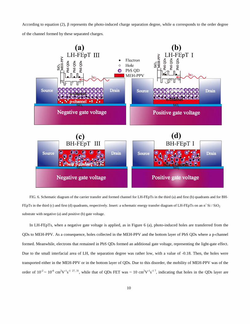
FIG. 6. Schematic diagram of the carrier transfer and formed channel for LH-FEpTs in the third (a) and first (b) quadrants and for BH-
FEpTs in the third (c) and first (d) quadrants, respectively. Insert: a schematic energy transfer diagram of LH-FEpTs on an n+ Si / SiO2
substrate with negative (a) and positive (b) gate voltage.
In LH-FEpTs, when a negative gate voltage is applied, as in Figure 6 (a), photo-induced holes are transferred from the
QDs to MEH-PPV. As a consequence, holes collected in the MEH-PPV and the bottom layer of PbS QDs where a p-channel
formed. Meanwhile, electrons that remained in PbS QDs formed an additional gate voltage, representing the light-gate effect.
Due to the small interfacial area of LH, the separation degree was rather low, with a value of -0.18. Then, the holes were
transported either in the MEH-PPV or in the bottom layer of QDs. Due to this disorder, the mobility of MEH-PPV was of the
order of 10-2
~ 10-6
cm2V
-1s
-1
27, 31, while that of QDs FET was ~ 10 cm
2V
-1s
-1 7, indicating that holes in the QDs layer are
11
transported more effectively than in MEH-PPV. Thus, the measured mobility (36 cm2V
-1s
-1) is mainly contributed by holes in
the QDs, which is also a reasonable value for mobility in QD FETs according to a prior report 32
.
When the positive gate voltage was applied, the carrier transferred to the homojunction interface instead of the
heterojunction interface due to the level mismatch between QDs and MEH-PPV. As the alignment of the energy level of the
QD layers occurred, as in Figure 6 (b), the separation degree improved to β = 0.026. After that, an n--channel formed in the
bottom layers of the PbS QDs. It has been reported that the pristine QD FEpTs also exhibited a photo response31
. For a
layered structure, the n-channel order degree is equivalent to the p-channel; then, a very close value of α is obtained. As a
consequence, a larger αμCox/L2 and a higher responsivity (10
1 A/W) are achieved by LH-FEpTs in the positive gate operating
region due to the high μ, high β and equivalent α.
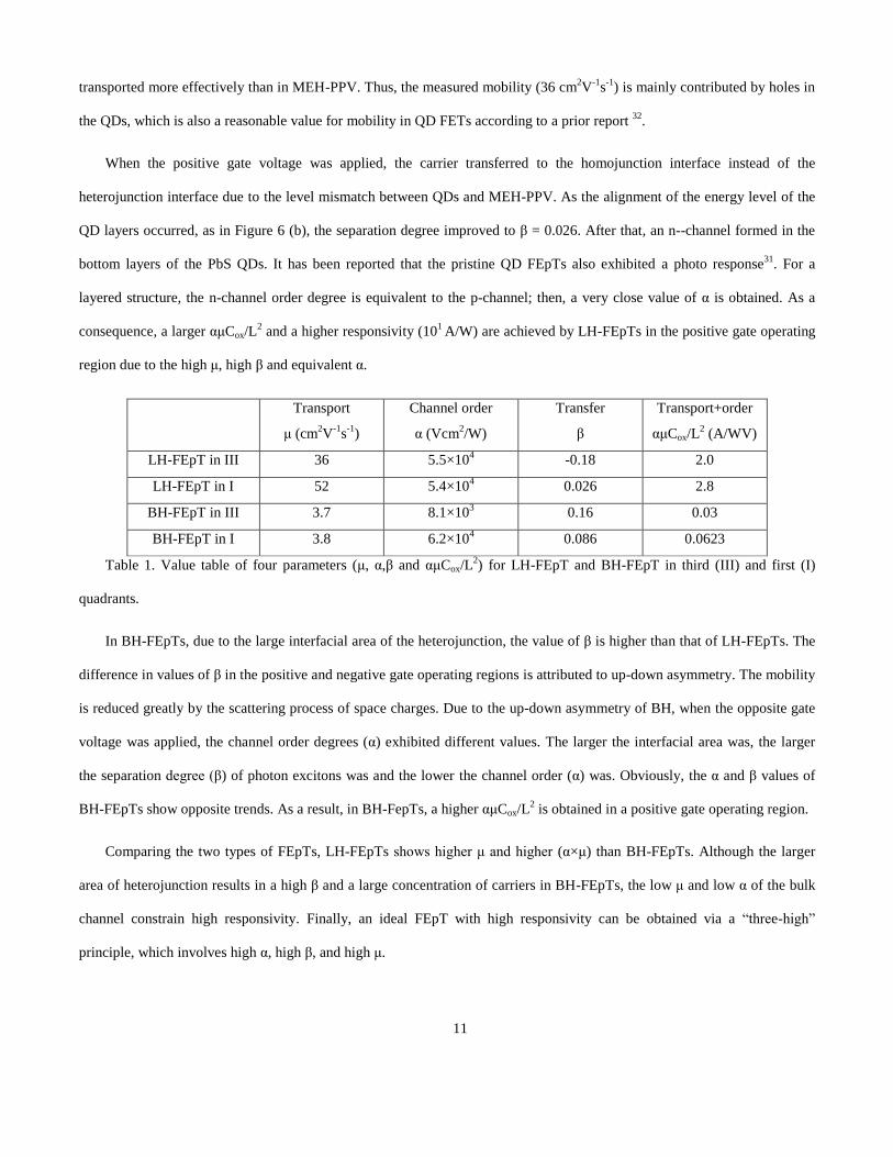
Transport
μ (cm2V
-1s
-1)
Channel order
α (Vcm2/W)
Transfer
β
Transport+order
αμCox/L2 (A/WV)
LH-FEpT in III 36 5.5×10⁴ -0.18 2.0
LH-FEpT in I 52 5.4×10⁴ 0.026 2.8
BH-FEpT in III 3.7 8.1×10³ 0.16 0.03
BH-FEpT in I 3.8 6.2×10⁴ 0.086 0.0623
Table 1. Value table of four parameters (μ, α,β and αμCox/L2) for LH-FEpT and BH-FEpT in third (III) and first (I)
quadrants.
In BH-FEpTs, due to the large interfacial area of the heterojunction, the value of β is higher than that of LH-FEpTs. The
difference in values of β in the positive and negative gate operating regions is attributed to up-down asymmetry. The mobility
is reduced greatly by the scattering process of space charges. Due to the up-down asymmetry of BH, when the opposite gate
voltage was applied, the channel order degrees (α) exhibited different values. The larger the interfacial area was, the larger
the separation degree (β) of photon excitons was and the lower the channel order (α) was. Obviously, the α and β values of
BH-FEpTs show opposite trends. As a result, in BH-FepTs, a higher αμCox/L2 is obtained in a positive gate operating region.
Comparing the two types of FEpTs, LH-FEpTs shows higher μ and higher (α×μ) than BH-FEpTs. Although the larger
area of heterojunction results in a high β and a large concentration of carriers in BH-FEpTs, the low μ and low α of the bulk
channel constrain high responsivity. Finally, an ideal FEpT with high responsivity can be obtained via a “three-high”
principle, which involves high α, high β, and high μ.
12
In summary, we investigated two types of FEpT NIR detectors based on a MEH-PPV and PbS QDs hybrid, LH-FEpTs
and BH-FEpTs. Bipolar characteristics were shown by both. The μH ≈ μE in BH-FEpTs is 3.7 cm2V
-1 s-1, and μH = 36 cm
2V
-1 s-
1, μE = 52 cm
2V
-1 s-1 in LH-FEpTs. Due to the greatly promoted mobility and highly ordered channels, the responsivity of LH-
FEpTs can reach as high as 101 A/W, whereas that of BH-FEpTs can be as low as 10
-1 A/W. Although the large area of BHs
shows a high separation degree of photo-excitons, the lack of an effective transport mechanism becomes the main restraining
factor. Therefore, LH-FEpTs are a better candidate for a NIR photo detector. Finally, an ideal FEpT with high responsivity is
obtained via a “three-high” principle with high α, high β, and high μ.
This work is supported by the National Natural Science Foundation of China (Grant No. 61271066) and the Foundation
of Independent Innovation of Tianjin University (Grant No. 60302070).
References 1. Y. Yang, W. Rodriguez-Cordoba and T. Lian, Nano Letters 12 (8), 4235-4241 (2012).
2. S. A. McDonald, G. Konstantatos, S. Zhang, P. W. Cyr, E. J. D. Klem, L. Levina and E. H. Sargent, Nat
Mater 4 (2), 138-142 (2005).
3. S. Zhang, P. W. Cyr, S. A. McDonald, G. Konstantatos and E. H. Sargent, Applied Physics Letters 87 (23),
- (2005).
4. G. Konstantatos, I. Howard, A. Fischer, S. Hoogland, J. Clifford, E. Klem, L. Levina and E. H. Sargent,
Nature 442 (7099), 180-183 (2006).
5. T. Rauch, M. Boberl, S. F. Tedde, J. Furst, M. V. Kovalenko, G. N. Hesser, U. Lemmer, W. Heiss and O.
Hayden, Nature Photonics 3 (6), 332-336 (2009).
6. W. Zhang, C.-P. Chuu, J.-K. Huang, C.-H. Chen, M.-L. Tsai, Y.-H. Chang, C.-T. Liang, Y.-Z. Chen, Y.-L.
Chueh, J.-H. He, M.-Y. Chou and L.-J. Li, Sci. Rep. 4 (2014).
7. F. Hetsch, N. Zhao, S. V. Kershaw and A. L. Rogach, Materials Today 16 (9), 312-325 (2013).
8. H. Yu, Z. Bao and J. H. Oh, Advanced Functional Materials 23 (5), 629-639 (2013).
9. W. Feng, C. Qin, Y. Shen, Y. Li, W. Luo, H. An and Y. Feng, Scientific Reports 4 (2014).
10. I. J. Kramer and E. H. Sargent, Chemical Reviews 114 (1), 863-882 (2014).
11. Y. Zhou, M. Eck and M. Kruger, Energy & Environmental Science 3 (12), 1851-1864 (2010).
12. H.-C. Liao, C.-S. Tsao, T.-H. Lin, M.-H. Jao, C.-M. Chuang, S.-Y. Chang, Y.-C. Huang, Y.-T. Shao, C.-Y.
Chen, C.-J. Su, U. S. Jeng, Y.-F. Chen and W.-F. Su, Acs Nano 6 (2), 1657-1666 (2012).
13. Z. Sun, J. Li and F. Yan, Journal of Materials Chemistry 22 (40), 21673-21678 (2012).
14. G. Konstantatos, M. Badioli, L. Gaudreau, J. Osmond, M. Bernechea, F. P. G. de Arquer, F. Gatti and F. H.
L. Koppens, Nat Nano 7 (6), 363-368 (2012).
15. Z. Sun, Z. Liu, J. Li, G.-a. Tai, S.-P. Lau and F. Yan, Advanced Materials 24 (43), 5878-5883 (2012).
13
16. W. Mingqing and W. Xiaogong, in Proceedings of ISES World Congress 2007 (Vol. I – Vol. V), edited by
D. Y. Goswami and Y. Zhao (Springer Berlin Heidelberg, 2009), pp. 1303-1307.
17. Y. Yang and T. Lian, Coordination Chemistry Reviews 263, 229-238 (2014).
18. J. Y. Kim, O. Voznyy, D. Zhitomirsky and E. H. Sargent, Advanced Materials 25 (36), 4986-5010 (2013).
19. Z. Yating, [URL will be inserted by AIP] (2014).
20. I. Kang and F. W. Wise, J. Opt. Soc. Am. B 14 (7), 1632-1646 (1997).
21. L. Britnell, R. V. Gorbachev, R. Jalil, B. D. Belle, F. Schedin, A. Mishchenko, T. Georgiou, M. I.
Katsnelson, L. Eaves, S. V. Morozov, N. M. R. Peres, J. Leist, A. K. Geim, K. S. Novoselov and L. A.
Ponomarenko, Science 335 (6071), 947-950 (2012).
22. R. Buonsanti and D. J. Milliron, Chemistry of Materials 25 (8), 1305-1317 (2013).
23. S. Z. Bisri, J. Gao, V. Derenskyi, W. Gomulya, I. Iezhokin, P. Gordiichuk, A. Herrmann and M. A. Loi,
Advanced Materials 24 (46), 6147-6152 (2012).
24. J. Li, L. Niu, Z. Zheng and F. Yan, Advanced Materials 26 (31), 5239-5273 (2014).
25. C. O. Kim, S. Kim, D. H. Shin, S. S. Kang, J. M. Kim, C. W. Jang, S. S. Joo, J. S. Lee, J. H. Kim, S.-H.
Choi and E. Hwang, Nat Commun 5 (2014).
26. B. N. Limketkai, P. Jadhav and M. A. Baldo, Physical Review B 75 (11), 113203 (2007).
27. L. Li, G. Meller and H. Kosina, J Comput Electron 6 (1-3), 357-361 (2007).
28. L.-L. Chua, J. Zaumseil, J.-F. Chang, E. C. W. Ou, P. K. H. Ho, H. Sirringhaus and R. H. Friend, Nature
434 (7030), 194-199 (2005).
29. L. Britnell, R. M. Ribeiro, A. Eckmann, R. Jalil, B. D. Belle, A. Mishchenko, Y.-J. Kim, R. V. Gorbachev,
T. Georgiou, S. V. Morozov, A. N. Grigorenko, A. K. Geim, C. Casiraghi, A. H. C. Neto and K. S. Novoselov,
Science 340 (6138), 1311-1314 (2013).
30. Z. Sun and H. Chang, Acs Nano 8 (5), 4133-4156 (2014).
31. H. Wang, Y. Zhang, X. Song, L. Jin, H. Dai, S. Wu and J. Yao, APPLIED MECHANICS AND
MATERIALS 668 - 669, 818-821 (2014).
32. D. S. Chung, J.-S. Lee, J. Huang, A. Nag, S. Ithurria and D. V. Talapin, Nano Letters 12 (4), 1813-1820
(2012).


