Embed Size (px)
Citation preview

IEEE TRANSACTIONS ON SEMICONDUCTOR MANUFACTURING, VOL. 17, NO. 4, NOVEMBER 2004 517
Acoustically Actuated FlextensionalSixNy and Single-Crystal Silicon 2-D
Micromachined Ejector ArraysUtkan Demirci, Student Member, IEEE, Goksen G. Yaralioglu, Member, IEEE, Edward Hæggström,
Gökhan Perçin, Member, IEEE, Sanli Ergun, Member, IEEE, and B. T. Khuri-Yakub, Fellow, IEEE
Abstract—We propose using two-dimensional (2-D) micro-machined droplet ejector arrays for environmentally benigndeposition of photoresist and other spin-on materials, such aslow- and high- dielectrics used in IC manufacturing. Direct de-position of these chemicals will reduce waste as well as productioncost. The proposed device does not harm heat or pressure sensitivefluids and they are chemically compatible with the materialsused in IC manufacturing. Each element of the 2-D ejector arrayconsists of a flexurally vibrating circular membrane on one face ofa cylindrical fluid reservoir. The membrane has an orifice at thecenter. A piezoelectric transducer generating ultrasonic waves,located at the open face of the reservoir, actuates the membranes.As a result of this actuation, droplets are fired through the mem-brane orifice. Ejector arrays were built with either Si N orsingle-crystal silicon membranes using two different fabricationprocesses. We show that single-crystal silicon membranes aremore uniform in their thickness and material quality than thoseof Si N membranes. The single-crystal silicon membrane-baseddevices showed thickness and material uniformity across all themembranes of an array. This improvement eliminated nonuniformmembrane resonance frequencies across an array as observed withSi N membrane-based devices. Therefore, it should be possibleto repeatably build devices and to predict their dynamic char-acteristics. Using the fabricated devices, we demonstrated waterejection at 470 kHz, 1.24 MHz, and 2.26 MHz. The correspondingdroplet diameters were 6.5, 5, and 3.5 m, respectively.
Index Terms—Deposition, droplet ejection, inkjet, microelec-tromechanical systems (MEMS), transducer, ultrasound, wafercoating.
I. INTRODUCTION
VARIOUS techniques have been reported for depositionof organic polymers such as photoresist, low- or high-
dielectrics in semiconductors, and microelectromechanicalsystems (MEMS) processes [1]. Spin coating is widely em-ployed in current applications, since it can fulfill the throughputand quality requirements of the IC industry [2]. However, this
Manuscript received September 23, 2003; revised May 26, 2004. The work ofE. Hæggström was supported in part by the Wihuri Foundation and the Academyof Finland.
U. Demirci and B. T. Khuri-Yakub are with the Department of ElectricalEngineering, Stanford University, Stanford, CA 94305-9505 USA (e-mail:[email protected]). They are also with the E. Ginzton Laboratory, StanfordUniversity, Stanford, CA 94305-4088 USA.
G. G. Yaralioglu, G. Perçin, and S. Ergun are with the E. Ginzton Laboratory,Stanford University, Stanford, CA 94305-4088 USA.
E. Hæggström is the E. Ginzton Laboratory, Stanford University, Stanford,CA 94305-4088 USA. He is also with the Department of Physics, University ofHelsinki, Helsinki FIN-00014, Finland.
Digital Object Identifier 10.1109/TSM.2004.835714
Fig. 1. Axisymmetric model of a unit cell for FEM simulations.
method causes extensive waste of expensive chemicals. Forinstance, photoresist deposition by spin coating wastes morethan 95% of the resist consumed during the process [1]. Inaddition to losing expensive chemicals, the cost of disposinghazardous waste is high [1]–[3]. Furthermore, this waste canpotentially pollute the environment. This waste can be reducedby direct deposition of the chemicals.
In manufacturing of semiconductors and MEMS, depositionof organic polymers by spin coating is the most employedprocess step [4]. Alternative deposition methods, such as de-position of doped organic polymers for organic devices, e.g.,light-emitting diodes (LEDs) and flat panel displays, and fordeposition of photoresist or dielectric materials for semicon-ductor manufacturing are emerging [5]. Moreover, a reliableand rapid method for dispensing femtoliters to picoliters offluid emerges as a basic need in the fields of biomedicine andbiotechnology [6]–[8].
Several methods for drop generation exist. One of thesemethods is inkjet printing [9]. The thermal ejection inkjet(bubble jet) is based on a fast heating of the ejection fluidand the subsequent formation of an expanding vapor bubble,which creates increasing pressure in the fluid reservoir [9].The fluid is pushed out of the reservoir through a nozzle asdroplets. However, the problem with thermal ejection for theapplications of interest here is that the heating may damageheat sensitive fluids such as photoresist and low- or high-dielectrics. Another ejection method is based on piezoelectricactuation, which involves the actuation of a piezoelectric ele-ment causing compression in the fluid volume and consequentlya corresponding increase in the pressure within the reservoir.
0894-6507/04$20.00 © 2004 IEEE

518 IEEE TRANSACTIONS ON SEMICONDUCTOR MANUFACTURING, VOL. 17, NO. 4, NOVEMBER 2004
TABLE ICHARACTERISTIC MATERIAL PROPERTY VALUES USED FOR FEM SIMULATIONS
This results in droplet ejection through a vertical or horizontalpointing nozzle. However, this method pressurizes the reser-voir at every ejection cycle with possible adverse effects onbarosensitive fluids. Moreover, both the aforementioned devicetypes are difficult to fabricate as two-dimensional (2-D) arrays[9], [11]. Furthermore, it is hard to reduce the printhead sizeand to increase the spatial density of the array elements usedin these two types of devices. In general, these devices workin the range of 10 to 100 kHz and eject 10–20- m-diameterdroplets [9].
Previously, various actuation methods have been used to ejectfluids from a small orifice in a membrane. Maehara et al. demon-strated an ultrasonic atomizer, where a piezoelectric actuatorlocated on top of a 50- m-thick circular membrane made ofsteel with an 80- m-diameter pinhole in the center generated70- m-diameter droplets [10]. Perçin et al. used a piezoelectricring fabricated on top of the membranes of a large-scale device,where the piezoelectric ring initiated the displacement of themembranes [12]–[15]. Although these methods allow the indi-vidual addressing of each array element, the fabrication processis difficult [11].
Coating of a wafer per se does not require individual ad-dressing of the array elements since it can be done by scanningan ejector array over a wafer. This allows us to use an externaltransducer that is not integrated to the membranes for actuation.
We propose to use acoustically actuated 2-D micromachinedejector arrays to deposit organic polymers onto wafers. Theejector array does not damage sensitive fluids and it producesequally sized droplets. Further, it does not fully pressurize thefluid and it is compatible with most chemicals. Moreover, the ar-rays operate in the megahertz frequency range. Therefore, theyprovide high flow rates and a capability to eject small dropletswithin the 3–7- m-diameter range.
We demonstrate fabrication of 2-d micromachined ejector ar-rays based on Si N and single-crystal silicon membranes. Wecompare the performance of these two types of ejector arraysdemonstrating uniform thickness and material devices. We alsodemonstrate ejection of solvents with various viscosity and sur-face tension as well as experimental ejection results of initialsatellite-free droplet generation.
II. THEORY
We use finite-element method (FEM) simulations (ANSYS5.71) to predict the resonant frequencies of the device. The FEMsimulations perform a harmonic analysis of the three–dimen-sional (3-D) axisymmetric structure shown in Fig. 1. The meshdensity is chosen so that there are at least ten nodes per wave-length in the structure. The device is simulated by loading oneside of a clamped membrane at the end of a fluid reservoir withan infinitely long fluid space. The undesired reflections from the
1ANSYS Inc., PA, USA.
Fig. 2. FEM results: Maximum orifice displacement versus frequency of a 2-Dmicromachined ejector of 100 �m in diameter 1 �m thick silicon and 300 �min diameter 2.1-�m-thick Si N membranes for 10-Pa uniform pressure overthe membranes.
end of the mesh are eliminated by absorbing boundary condi-tions (FLUID 129). The structure–fluid interaction is taken intoaccount by solid/fluid interface elements (FLUID 29). As a con-stant pressure is applied on the membrane at varying frequen-cies, the displacement at the orifice is monitored as a function offrequency. The simulations are performed with both the Si Nand single-crystal silicon membranes by changing the materialproperties of the device. The characteristic material values usedin the simulations are shown in Table I [16].
It is important to determine the resonant frequencies of thedevice, since at these resonances, the displacement of the ori-fice is maximal. If this displacement is larger than the criticalminimum displacement required for breaking a droplet fromthe orifice, the fluid is ejected through the orifice [13]. Theorifice displacement as a function of frequency for Si N andsingle-crystal silicon membranes is shown in Fig. 2, assuming a10-Pa uniform pressure across the membranes. Our FEM sim-ulations predict the first, second, and third resonances of themembrane to be at 650 kHz, 1.39 MHz, 2.42 MHz, for 300 min diameter, and 2.1- m-thick Si N membranes. The first andsecond resonances are at 1.27 MHz, 2.16 MHz for 100 m indiameter, and 1- m-thick single-crystal silicon membranes.
III. DEVICE
A. Design
A flexurally vibrating circular membrane located at one faceof a through-wafer hole etched in a wafer constitutes the unit cellof a 2-D ejector array as shown in Fig. 3. The 2-D ejector arrayis formed by replication of this unit cell as shown in Fig. 4. The
DEMIRCI et al.: ACOUSTICALLY ACTUATED FLEXTENSIONAL Si N 519
Fig. 3. Unit cell of 2-D micromachined ejector array.
Fig. 4. Geometry of 2-D micromachined ejector array.
thickness of the wafer and the diameter of the through-waferhole determine the height of the fluid reservoir and the mem-brane diameter, respectively. An orifice is etched in the centerof the circular membrane so that fluid in the cylindrical reser-voir is fired through this orifice as droplets when the membraneis actuated.
The actuation of the device is done acoustically. A piezoelec-tric transducer (A306S or A303S2) is placed coaxially with themembrane with its acoustic axis orthogonal to the open face ofthe reservoir at a controllable distance within 0–2-cm range. Asthe generated ultrasonic waves travel through the fluid reser-voir and reach the clamped circular membrane, the vibratingmembrane generates capillary waves on the liquid surface of theair/liquid interface at the orifice and raises the pressure on theinterface without compressing the reservoir [13]. This pressureshould overcome the restoring forces of the surface tension ofthe liquid in order to initiate ejection.
B. Fabrication
The 2-D micromachined ejector arrays are fabricated by stan-dard IC manufacturing processes.
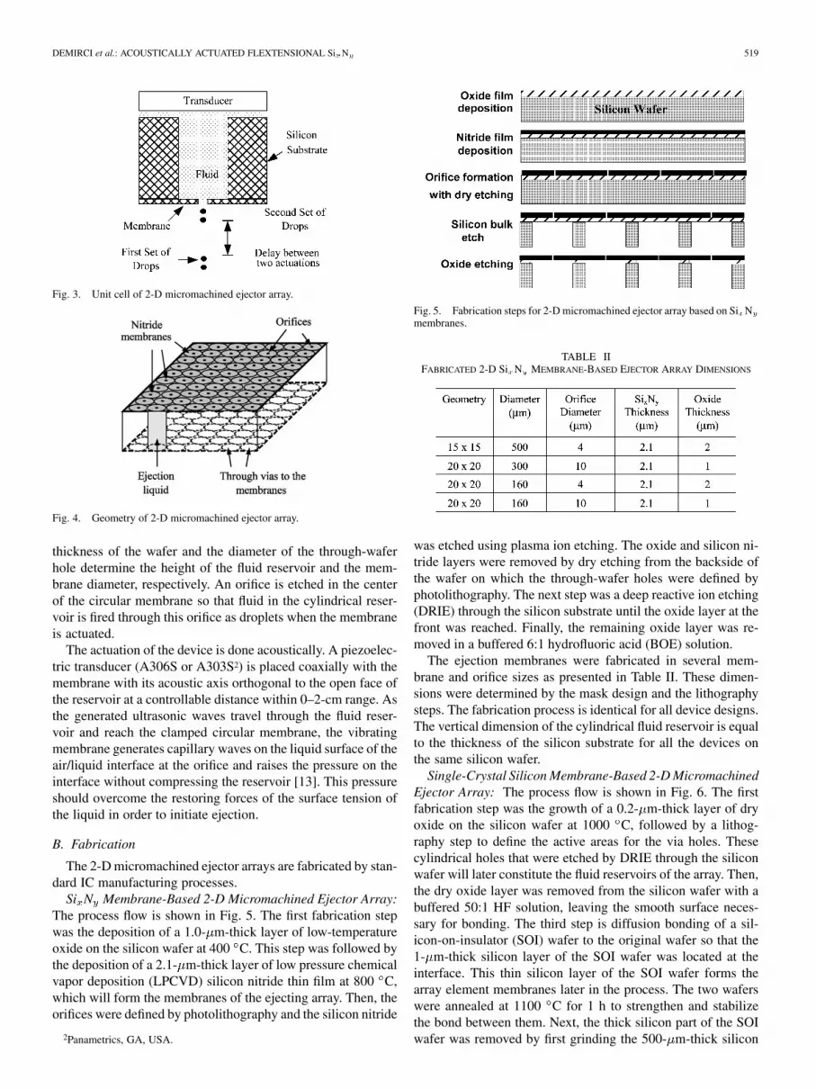
Si N Membrane-Based 2-D Micromachined Ejector Array:The process flow is shown in Fig. 5. The first fabrication stepwas the deposition of a 1.0- m-thick layer of low-temperatureoxide on the silicon wafer at 400 C. This step was followed bythe deposition of a 2.1- m-thick layer of low pressure chemicalvapor deposition (LPCVD) silicon nitride thin film at 800 C,which will form the membranes of the ejecting array. Then, theorifices were defined by photolithography and the silicon nitride
2Panametrics, GA, USA.
Fig. 5. Fabrication steps for 2-D micromachined ejector array based on Si Nmembranes.
TABLE IIFABRICATED 2-D Si N MEMBRANE-BASED EJECTOR ARRAY DIMENSIONS
was etched using plasma ion etching. The oxide and silicon ni-tride layers were removed by dry etching from the backside ofthe wafer on which the through-wafer holes were defined byphotolithography. The next step was a deep reactive ion etching(DRIE) through the silicon substrate until the oxide layer at thefront was reached. Finally, the remaining oxide layer was re-moved in a buffered 6:1 hydrofluoric acid (BOE) solution.
The ejection membranes were fabricated in several mem-brane and orifice sizes as presented in Table II. These dimen-sions were determined by the mask design and the lithographysteps. The fabrication process is identical for all device designs.The vertical dimension of the cylindrical fluid reservoir is equalto the thickness of the silicon substrate for all the devices onthe same silicon wafer.
Single-Crystal Silicon Membrane-Based 2-D MicromachinedEjector Array: The process flow is shown in Fig. 6. The firstfabrication step was the growth of a 0.2- m-thick layer of dryoxide on the silicon wafer at 1000 C, followed by a lithog-raphy step to define the active areas for the via holes. Thesecylindrical holes that were etched by DRIE through the siliconwafer will later constitute the fluid reservoirs of the array. Then,the dry oxide layer was removed from the silicon wafer with abuffered 50:1 HF solution, leaving the smooth surface neces-sary for bonding. The third step is diffusion bonding of a sil-icon-on-insulator (SOI) wafer to the original wafer so that the1- m-thick silicon layer of the SOI wafer was located at theinterface. This thin silicon layer of the SOI wafer forms thearray element membranes later in the process. The two waferswere annealed at 1100 C for 1 h to strengthen and stabilizethe bond between them. Next, the thick silicon part of the SOIwafer was removed by first grinding the 500- m-thick silicon

520 IEEE TRANSACTIONS ON SEMICONDUCTOR MANUFACTURING, VOL. 17, NO. 4, NOVEMBER 2004
Fig. 6. Fabrication steps for 2-D single-crystal silicon membrane-basedejector array using wafer bonding approach.
part to 100 m and then by performing a 2-h wet silicon etch intetramethylammonium hydroxide (TMAH) at 85 C that stopsat the 4- m-thick SOI oxide layer. Later, the oxide layer was re-moved in a buffered 50:1 HF solution. Finally, the orifices weredefined by photolithography and the silicon was etched usingplasma ion etching.
The time required for DRIE to open a via hole depends on thewafer thickness and of the active area. The etch took 4 h withthe 500- m-thick silicon wafer, where the active areas coveredone-third of the 4-in wafer. The resist to silicon selectivity ofthe DRIE is high (75:1). A 7–10- m-thick resist was chosen toact as the first masking layer to be able to etch through waferholes in a 500- m-thick wafer. However, during this long etchprocess the photoresist mask will burn and lose its sharpnessat the edges. Due to the high selectivity of the DRIE to siliconoxide (100:1), the dry oxide layer acts as a second mask. There-fore, the dry oxide layer growth as a first step is crucial for thefabrication process.
Varying membrane sizes result in nonuniform resonance fre-quencies, membrane displacements, and droplet sizes [17]. Un-successful bonding thus results in a nonuniform array defeatingthe purpose of using an SOI wafer to fabricate membranes ofuniform thickness and size. Fortunately, the bonding quality canbe monitored by an infrared (IR) camera and an unsuccessfulbonding can be repeated [18].
The significance of the bonding step merits extra care to re-duce the surface roughness on the bonding surfaces. However,the surface of a silicon wafer that will be bonded to a SOI wafergoes through a long DRIE step. The dry oxide layer used asa mask also protects the smoothness of the surface. After theDRIE step, the dry oxide layer is removed by a wet etch in abuffered oxide etch (50:1, BOE), leaving a smooth surface readyfor bonding. If the roughness at the silicon surface is still endan-gering the success of the bonding step, a short 0.1- m chemicalmechanical polishing (CMP) step can smoothen the surface toachieve successful bonding.
Two-dimensional micromachined arrays fabricated in sev-eral membrane and orifice sizes are presented in Table III. A5 5 100- m-diameter single-crystal silicon membrane-basedejector array is presented in Fig. 7. The fabrication process
TABLE III2-D SINGLE-CRYSTAL SILICON EJECTOR ARRAY DIMENSIONS
WITH WAFER BONDING TECHNIQUE
Fig. 7. 5� 5 100-�m-diameter single-crystal silicon membrane-based 2-Dmicromachined ejector arrays.
Fig. 8. Block diagram of experimental setup.
was identical for all device designs. The vertical dimensionof the cylindrical fluid reservoir was equal to the thicknessof the silicon substrate for all devices on the same siliconwafer. The lateral dimensions of the devices such as membranediameters and pitch were determined by the mask design andthe lithography steps.
IV. EXPERIMENT
A. Methods
A block diagram of the experimental setup is shown in Fig. 8.The LEDs are turned on by a periodic square pulse waveform,which is synchronized with the transducer drive signal. Onedroplet is ejected during each period of the input signal. Thedroplets are sampled at the same rate that they are generated.By this stroboscopic imaging technique, the droplets can beviewed by the LCD camera (Sony, SSC-CD33V) as stationaryon the monitor screen. A vertical micrometer stage controls theseparation between the transducer and the device ranging from

DEMIRCI et al.: ACOUSTICALLY ACTUATED FLEXTENSIONAL Si N 521
Fig. 9. Block diagram of droplet imaging setup.
0 to 2 cm as shown in Fig. 9. The 2-D ejector array is set ona tilt stage. The function of the tilt stage is to align the trans-ducer surface parallel to the ejector membrane surface to facili-tate the formation of standing waves between the device and thetransducer.
The droplet sizes on the screen were determined by mon-itoring objects of known dimensions on the screen to derivea conversion chart valid for several distances. By using thischart, the size and separation of the ejected droplets were mea-sured from the pictures obtained from the monitor screen. Thetime difference between the generations of two droplets is equalto a single period of the transducer. The droplet velocity wasdetermined by dividing the distance between two consecutivedroplets by the time it took to generate a single droplet. Theerror margin for the droplet size was obtained from the sharp-ness of the image on the monitor screen. The blurred rim of thedroplet images had a thickness of 0.5 m, giving the resultingerror margins. The flow rate was calculated by multiplying thevolume of a single droplet with the frequency of ejection.
B. Results
These ejector arrays were observed to eject distilled water,isopropanol, acetone, and ethyl alcohol. The data presented inthis paper is from the experiments with distilled water. Dropletsize and droplet speed at resonance frequencies of 470 kHz,1.24 MHz, and 2.26 MHz were experimentally observed withSi N membranes. This is within 10% of the values predictedby the FEM simulations at higher resonance frequencies asshown in Table IV. An ejection summary is presented inTable IV. Droplets ejected at 1.24 MHz are shown in Fig. 10.Multiple simultaneous ejections from two adjacent membranesof the 20 20 2-D micromachined ejector array are shown inFig. 11. The ejection was observed in continuous mode. Thedroplet generation was turned on and off by activating anddeactivating the transducer.
Droplets ejected from the single-crystal silicon membranes at1.2 MHz are shown in Figs. 12 and 13 from two array elementsof the same 5 5 2-D micromachined ejector array with 100 min diameter membranes. All the ejecting array elements wereobserved on the monitor to have an identical second resonantmode shape at 1.2 MHz, indicating the uniformity of the array,as can be seen in Figs. 12 and 13.
TABLE IVEXPERIMENTAL DATA: EJECTION SUMMARY
FOR Si N MEMBRANE-BASED EJECTORS
Fig. 10. Stationary 5 �m in diameter droplets ejected at 1.24 MHz from300-�m-diameter Si N membranes with 10 �m in diameter orifices.
Fig. 11. Multiple simultaneous ejections at 1.24 MHz from 300-�m-diameterSi N membranes with 10 �m in diameter orifices.
A single ejector array membrane was observed to be capableof ejecting at three resonances. The droplet diameter generatedby the same membrane decreased with increased ejection fre-quency as shown in Fig. 14. Moreover, the droplet ejection speedalso increased with increased ejection frequency as shown inFig. 15. A simple fit as a function of the frequency is shown inFigs. 14 and 15.
C. Discussion
The strength of the single-crystal silicon membrane fabrica-tion process is the capability to repeatably fabricate uniformarrays. The thin silicon layer of the SOI wafer ensures thatthe membrane material is single-crystal silicon for all array

522 IEEE TRANSACTIONS ON SEMICONDUCTOR MANUFACTURING, VOL. 17, NO. 4, NOVEMBER 2004
Fig. 12. Ejection at 1.2 MHz by 100-�m-diameter membranes with10-�m-diameter orifices.
Fig. 13. Ejection at 1.2 MHz by 100-�m-diameter membranes with10-�m-diameter orifices.
elements, whereas the previously fabricated Si N mem-brane-based arrays were observed to suffer from bubbleformation in the Si N layer resulting in a nonuniform mem-brane material. Another uniformity measure is the membranethickness variation. The single-crystal silicon membranes are1- m thick with a 6 standard deviation variation of 0.024 mover an array [19]. This uniformity is observed to be poorerfor the fabricated Si N membrane-based arrays. Moreover,single-crystal silicon membranes are stress free, whereas Si Nmembrane stresses will shift the membrane resonance. Mostimportantly, the stress, deposition thickness, material unifor-mity, and thin-film quality varies from process to process inthe Si N -based array process, whereas the repeatability of theprocess is ensured with a single-crystal silicon membrane-basedarray process.
The directionality of the ejection is an important parameter.The images in Figs. 12 and 13 were taken with the same cameratilt angle of 45 without changing the camera location. By in-vestigating the ejection angle in both of the figures we concludethat these two membranes are not ejecting in the same direction.
The contact angle between the membrane and the liquid de-termines how it wets the orifice. The directionality of the jetdepends on the initial shape of the fluid surface at the orifice,the pressure distribution in the fluid reservoir, and uniformity ofthe orifice shape [20]. If the fluid has initially wetted the ori-fice asymmetrically, ejection with an angle to the normal of themembrane surface may be observed. When all the orifices havebeen wetted by initial ejection cycles, this effect is minimized.Secondly, the transducer should actuate the device such that thepressure distribution in all the fluid reservoirs of the array is thesame. An identical pressure distribution in the reservoirs couldensure an identical actuation of all of the membranes, and thusidentical droplet sizes, speeds, and directionality. Thirdly, thelithography step and DRIE ensure the geometrical uniformityof the orifice shape.
Fig. 14. Droplet diameter versus frequency for 300-�m-diameter 10-�morifice diameter Si N membranes.
Fig. 15. Droplet speed versus frequency for 300-�m-diameter 10-�m orificediameter Si N membranes.
The droplet size and ejection speed depend on the propertiesof the fluid (72 dynes/cm, 0.89 cP for water @ 25 C [16]), thesize of the orifice, and the displacement of the membrane at theorifice. The droplet diameter is experimentally observed to de-crease with increasing actuation frequency as shown in Fig. 14.For a simple analysis, we assume that the orifice spans a cylinderof water as it displaces and that the water cylinder ejected fromthe orifice transforms into a water droplet due to surface ten-sion [21], [22]. A decrease in the droplet size is expected withincreasing frequency since the displacement at the orifice is re-duced at higher resonance frequencies as seen in Fig. 2. Thisimplies that the height of the cylinder is less for the same ori-fice area at higher frequencies. Hence, its volume is smaller,resulting in smaller droplets as seen in Table IV. The dropletejection speed is experimentally observed to increase with fre-quency as seen in Fig. 15. This can be understood by associ-ating a large droplet mass at low frequencies with a smaller ejec-tion speed and a small droplet mass at high frequencies with alarge ejection speed to have momentum conservation. We as-sume that same momentum is transferred in both cases to theliquid cylinder by the moving membrane.

DEMIRCI et al.: ACOUSTICALLY ACTUATED FLEXTENSIONAL Si N 523
Our proposed deposition method provides fast surface cov-erage since the ejection frequencies are in the megahertz range.Moreover, the device can be operated to deposit a specificnumber of droplets at a desired location. This effective dropletejection method should be able to solve some of the practicalproblems associated with the spin coating technique. One suchproblem is the inability to cover deep trenches with uniformphotoresist. This method places as many droplets as desired atany chosen location. This means that the waste is minimized.Since the waste is reduced, fabrication costs decrease, meaningincreased productivity and reduced environmental burden.
V. CONCLUSION
In summary, we demonstrated ejection of water with 2-D mi-cromachined ejector arrays based on Si N and single-crystalsilicon membranes. The higher structural uniformity of thesingle-crystal silicon membrane-based array compared to theSi N membrane-based array was demonstrated as well bythe capability to simultaneously eject from several membraneson the same array at the same frequency, as the similarity ofthe mode shapes observed on the membranes. High-frequencyoperation was presented, showing that it is possible to attainhigh flow and deposition rates. Future work will focus onphotoresist ejection, analysis of operation, and optimization ofthe 2-D micromachined ejector array design.
ACKNOWLEDGMENT
The authors would like to thank NSF/SRC Engineering Re-search Center for Environmentally Benign Semiconductor Man-ufacturing for their support on this research.
REFERENCES
[1] B. Bednar, J. Kralicek, and J. Zachoval, Resists in Microlithography andPrinting. Amsterdam, The Netherlands: Elsevier, 1993, pp. 77–82.
[2] J. Derksen, S. Han, and J.-H. Chun, “Extrusion spin coating: An efficientphotoresist coating process for wafers,” in Proc. Semiconductor Manu-facturing Conf., IEEE Int. Symp., Oct., 11–13 1999, pp. 245–248.
[3] G. Perçin, T. Lundgren, and B. T. Khuri-Yakub, “Photoresist depositionwithout spinning,” IEEE Trans. Semiconduct. Manufact., vol. 16, pp.452–459, Aug. 2003.
[4] L. M. Peurrung and D. B. Graves, “Spin coating over topography,” IEEETrans. Semiconduct. Manufact., vol. 6, pp. 72–76, Feb. 1993.
[5] T. R. Hebner, C. C. Wu, D. Marcy, M. H. Lu, and J. C. Strum, “Ink-jetprinting of doped polymers for organic light emitting devices,” Appl.Phys. Lett., vol. 72, no. 5, pp. 519–521, 1998.
[6] C. M. Roth and M. L. Yarmush, “Nucleic acid biotechnology,” Ann. Rev.Biomed. Eng., vol. 1, pp. 265–297, 1999.
[7] J. M. Jaklevic, H. R. Garner, and G. A. Miller, “Instrumentation for thegenome project,” Ann. Rev. Biomed. Eng., vol. 1, pp. 265–297, 1999.
[8] P. Luginbuhl, P. F. Indermuhle, M. A. Gretillat, F. Willemin, N. F. deRooij, D. Gerber, G. Gervasio, J. L. Vuilleumier, D. Twerenbold, M.Duggelin, and R. Guggenheim, “Micromachined injector for DNA massspectrometry,” in Proc. Transducers’99, pp. 1130–1133.
[9] H. P. Le, “Progress and trends in inkjet printing technology,” J. ImagingSci. Technol., vol. 42, no. 1, pp. 49–62, 1998.
[10] N. Maehara and S. Ueha, “Influence of the vibrating system of a mul-tipinhole-plate ultrasonic nebulizer on its performance,” Mori, Rev. Sci.Instrum., vol. 57, no. 11, pp. 2870–2876, 1986.
[11] G. Perçin, “Micromachined piezoelectrically actuated flextensionaltransducers for high resolution printing and imaging,” Ph.D. disserta-tion, Stanford University, Stanford, CA, 2002.
[12] G. Perçin, L. Levin, and B. T. Khuri-Yakub, “Piezoelectrically actuateddroplet ejector,” Rev. Sci. Instrum., vol. 68, pp. 4561–4563, 1997.
[13] G. Perçin, T. Lundgren, and B. T. Khuri-Yakub, “Controlled ink-jetprinting and deposition of organic polymers and solid particles,” Appl.Phys. Lett., vol. 73, no. 16, pp. 2375–2377, 1998.
[14] G. Perçin and B. T. Khuri-Yakub, Rev. Sci. Instrum., vol. 74, no. 2, pp.1120–1127, 2003.
[15] G. Perçin, A. Atalar, F. L. Degertekin, and B. T. Khuri-Yakub,“Micromachined two-dimensional array piezoelectrically actuatedtransducers,” Appl. Phys. Lett., vol. 72, no. 11, pp. 1397–1399, 1998.
[16] CRC Materials Science and Engineering.[17] A. W. Leissa, Vibration of Plates: Scientific Technical Information Div.,
Office of Technology Utilization, NASA, 1969, pp. 1G–10G.[18] U. Gosele, M. Alexe, P. Kopperschmidt, and Q.-Y. Tong, “Semicon-
ductor wafer bonding: A flexible approach to materials combinations inmicroelectronics, micromehanics and optoelectronics,” in Proc. Semi-conductor Conf. CAS, 1997, pp. 23–32.
[19] Datasheet for SOI Wafers, Aug. 2003.[20] E. R. Lee, Microdrop Generation. Boca Raton, FL: CRC, 2003.[21] S. A. Elrod, B. Hadimlioglu, B. T. Khuri-Yakub, E. G. Rawson, E.
Richley, C. F. Quate, N. N. Mansour, and T. S. Lundgren, “Nozzlelessdroplet formation with focused acoustic beams,” J. Appl. Phys., vol. 65,pp. 3441–3447, 1989.
[22] F. R. S. Rayleigh, “On the stability of Jets,” in Proc. London Math. Soc.,vol. 10, 1878, pp. 4–13.
Utkan Demirci (S’01) received the B.S. degree inelectrical engineering (summa cum laude) from theUniversity of Michigan, Ann Arbor, in 1999 and theM.S. degree from Stanford University, Stanford, CA,in 2001. He is currently working toward the Ph.D. de-gree in electrical engineering at Stanford University.
His research interests include MEMS, especiallymicromachined ultrasonic microfluid droplet ejectorarrays for high resolution printing and biological ap-plications, capacitive micromachined ultrasonic ar-rays (CMUTS) for medical imaging applications, and
two-dimensional acoustic ordered crystals.Mr. Demirci was a James B. Angell Scholar. He is one of the few recipients of
the Full Presidential Scholarship given by the Turkish Ministry of Education. Heis a corecipient of the 2002 Outstanding Paper Award of the IEEE Ultrasonics,Ferroelectrics and Frequency Control Society. He was the winner of StanfordUniversity Entrepreneur’s Challenge Competition in 2004. He is a member ofPhi Kappa Phi and the National Honor Society.
Goksen G. Yaralioglu (S’93–M’99) was born inAkhisar, Turkey, on May 13, 1970. He receivedthe B.S., M.S., and Ph.D. degrees from BilkentUniversity, Ankara, Turkey, in 1992, 1994, and 1999,respectively, all in electrical engineering.
He is now working as an Engineering Research As-sociate in the E. L. Ginzton Laboratory, Stanford Uni-versity, Stanford, CA. His current research interestsinclude design, modeling, and applications of micro-machined ultrasonic transducers and atomic force mi-croscopy at ultrasonic frequencies.
Edward Hæggström received the D.Sc. degree inapplied physics from the University of Helsinki,Helsinki, Finland, in 1998 and the M.B.A. degree ininnovation management from the Helsinki Univer-sity of Technology, Helsinki, in 2001.
He is a Visiting Scholar at E. L. Ginzton Labo-ratory, Stanford University, Stanford, CA, on leavefrom his position as Assistant Professor at the De-partment of Physics, University of Helsinki. His re-search interests include ultrasonic characterization ofbiological samples.

524 IEEE TRANSACTIONS ON SEMICONDUCTOR MANUFACTURING, VOL. 17, NO. 4, NOVEMBER 2004
Gökhan Perçin (S’92–M’00) was born in Ezine,Çanakkale, Turkey. He received the B.S. degree inelectrical and electronics engineering from BilkentUniversity, Ankara, Turkey in 1994. He received theM.S. and the Ph.D. degrees in electrical engineering,in 1996 and 2002, respectively, both from StanfordUniversity, Stanford, CA.
He worked at Numerical Technologies, Inc., SanJose, CA, as a Senior Engineer developing optical mi-crolithography software for rule-based optical prox-imity correction and photoresist modeling. He also
worked at Microbar Inc., Sunnyvale, CA, as the director of MEMS technologyand applications. He is Co-Founder and Board Director of ADEPTIENT, PaloAlto, CA. He has years of experience in the areas of fluid ejection, microflu-idics, micromachining, micromachined electromechanical systems, ultrasonicactuators, ultrasound transducers, biomedical imaging, software development,sensors, and actuators.
Dr. Perçin is a member of The Electrochemical Society and the AmericanVacuum Society.
Sanli Ergun (M’00) was born in Ankara, Turkey, in1969. He received the B.Sc., M.Sc., and Ph.D. de-grees in 1991, 1994, and 1999, respectively, all inelectrical and electronics engineering from BilkentUniversity, Ankara.
He is now with the E. L. Gizton Laboratory, Stan-ford University, Stanford, CA, as an EngineeringResearch Associate. His research interests includeacoustics, ultrasound, MEMS, and microwaveelectronics.
B. T. Khuri-Yakub (S’70–S’73–M’76–SM’87–F’95) was born in Beirut, Lebanon. He received theB.S. degree in 1970 from the American Universityof Beirut, the M.S. degree in 1972 from Dart-mouth College, and the Ph.D. degree in 1975 fromStanford University, Stanford, CA, all in electricalengineering.
He joined the research staff at the E. L. GinztonLaboratory, Stanford University in 1976 as a Re-search Associate. He was promoted to a SeniorResearch Associate in 1978 and to a Professor of
Electrical Engineering (Research) in 1982. He has served on many universitycommittees in the School of Engineering and the Department of ElectricalEngineering. Presently, he is the Deputy Director of the E. L. Ginzton Labo-ratory. He has been teaching both at the graduate and undergraduate levels forover 15 years, and his current research interests include in situ acoustic sensors(temperature, film thickness, resist cure, etc.) for monitoring and control ofintegrated circuits manufacturing processes, micromachining silicon to makeacoustic materials and devices such as airborne and water immersion ultrasonictransducers and arrays, fluid ejectors, and ultrasonic nondestructive evaluationand acoustic imaging and microscopy. He has authored over 300 publicationsand has been principal inventor or co-inventor of 54 issued patents.
Dr. Khuri-Yakub is a Senior Member of the Acoustical Society of Americaand a Member of Tau Beta Pi. He is an Associate Editor of Research in Non-destructive Evaluation, a journal of the American Society for NondestructiveTesting. He received the Stanford University School of Engineering Distin-guished Advisor Award, June 1987, and the Medal of the City of Bordeaux forcontributions to NDE, in 1983.


![Molecular Characterization of Type II Transposable Elements in Cowpea [\u0026lt;i\u0026gt;Vigna unguiculata\u0026lt;/i\u0026gt; (L.) Walp]](https://img.pdfslide.net/doc/110x75/6344b619596bdb97a9089621/molecular-characterization-of-type-ii-transposable-elements-in-cowpea-u0026ltiu0026gtvigna.jpg)