Embed Size (px)
Citation preview
Stereo PDM to I2S/TDM Converter Data Sheet ADAU7112
Rev. 0 Document Feedback Information furnished by Analog Devices is believed to be accurate and reliable. However, no responsibility is assumed by Analog Devices for its use, nor for any infringements of patents or other rights of third parties that may result from its use. Specifications subject to change without notice. No license is granted by implication or otherwise under any patent or patent rights of Analog Devices. Trademarks and registered trademarks are the property of their respective owners.
One Technology Way, P.O. Box 9106, Norwood, MA 02062-9106, U.S.A. Tel: 781.329.4700 ©2019 Analog Devices, Inc. All rights reserved. Technical Support www.analog.com
FEATURES 2 channels of PDM audio inputs from digital microphones 64× decimation ratio of PDM to PCM audio data 24-bit resolution to support high sound pressure level (SPL)
microphones 126 dB A-weighted SNR 4 kHz to 96 kHz output sampling rate Bit clock rates of 64×, 128×, 192×, 256×, 384×, or 512× the
output sampling rate Automatic PDM clock generation Automatic power-down when BCLK is removed 0.36 mA DVDD operating current at 48 kHz sampling rate
and 1.8 V supply Slave I2S or TDM output interface Up to TDM-16 supported Configurable TDM slots I/O supply voltage from 1.70 V to 3.63 V DVDD core supply voltage from 1.10 V to 1.98 V 4 μA typical DVDD shutdown current 9-ball, 1.26 mm × 1.26 mm, 0.4 mm pitch WLCSP Power-on reset
APPLICATIONS Mobile computing Portable electronics Consumer electronics Professional electronics
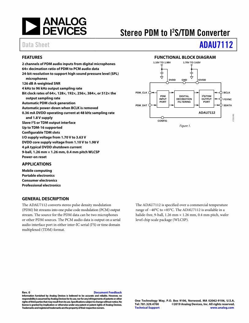
FUNCTIONAL BLOCK DIAGRAM
PDM_CLK
GND
1.70V TO 3.63V
IOVDD
1.10V TO 1.98V
DVDD
PDM_DAT
BCLK
FSYNC
SDATA
PDMINPUTPORT
DIGITALDECIMATIONFILTERING
ADAU7112
I2S/TDMOUTPUT
PORT
CONFIG 1723
2-00
1
Figure 1.
GENERAL DESCRIPTION The ADAU7112 converts stereo pulse density modulation (PDM) bit streams into one pulse code modulation (PCM) output stream. The source for the PDM data can be two microphones or other PDM sources. The PCM audio data is output on a serial audio interface port in either inter-IC serial (I2S) or time domain multiplexed (TDM) format.
The ADAU7112 is specified over a commercial temperature range of −40°C to +85°C. The ADAU7112 is available in a halide-free, 9-ball, 1.26 mm × 1.26 mm, 0.4 mm pitch, wafer level chip scale package (WLCSP).
ADAU7112 Data Sheet
Rev. 0 | Page 2 of 14
TABLE OF CONTENTS Features .............................................................................................. 1 Applications ....................................................................................... 1 Functional Block Diagram .............................................................. 1 General Description ......................................................................... 1 Revision History ............................................................................... 2 Specifications ..................................................................................... 3
Serial Port Timing Specifications ............................................... 4 PDM Input Timing Specifications ............................................. 5
Absolute Maximum Ratings ............................................................ 6 Thermal Resistance ...................................................................... 6 ESD Caution .................................................................................. 6
Pin Configuration and Function Descriptions ..............................7 Typical Performance Characteristics ..............................................8 Theory of Operation .........................................................................9
Power-Up and Initialization .........................................................9 Clocking ..........................................................................................9 Power-Down State .........................................................................9 Serial Audio Output Interface .....................................................9
Applications Information .............................................................. 13 Outline Dimensions ....................................................................... 14
Ordering Guide .......................................................................... 14
REVISION HISTORY 6/2019—Revision 0: Initial Version
Data Sheet ADAU7112
Rev. 0 | Page 3 of 14
SPECIFICATIONS DVDD = 1.10 V to 1.98 V, IOVDD = 1.70 V to 3.63 V, TA = 25°C, unless otherwise noted.
Table 1. Parameter Min Typ Max Unit Test Conditions/Comments DIGITAL INPUT
Input Voltage High Level (VIH) 0.7 ×
IOVDD V
Low Level (VIL) 0.3 × IOVDD
V
Input Leakage Digital input pins with pull-down resistor High Level (IIH) 2.5 μA Low Level (IIL) at 0 V 1 μA
Input Capacitance (CI) 2 pF Guaranteed by design DIGITAL OUTPUT
Output Voltage High Level (VOH) 0.85 ×
IOVDD V Source current when output is high (IOH) = 1 mA
Low Level (VOL) 0.1 × IOVDD
V Source current when output is low (IOL) = 1 mA
Digital Output Pins, Output Drive
The digital output pins are driving low impedance printed circuit board (PCB) traces to a high impedance digital input buffer
IOVDD = 1.8 V Nominal Drive Strength 2.8 mA
IOVDD = 3.3 V Nominal Drive Strength 10 mA
PERFORMANCE Dynamic Range 126 dB 20 Hz to 20 kHz, −60 dB input, A-weighted filter
(rms), relative to 0 dBFS output Signal-to-Noise Ratio
(SNR) 126 dB A-weighted filter, fifth-order input, relative to
0 dBFS output Decimation Ratio 64× Only 64× is supported Frequency Response −0.1 +0.01 dB DC to 0.45 × output sampling rate Stop Band 0.566 × output
sampling rate (fS)
Hz
Stop Band Attenuation 75 dB Group Delay 4.47 4.47 4.47 FSYNC cycles 0.02 fS input signal Gain 0 0 0 dB PDM to PCM Start-Up Time 63 64 64 FSYNC cycles After power-up reset and initialization code is run Bit Resolution 24 Bits Internal and output Interchannel Phase 0 0 0 Degrees
CLOCKING Output Sampling Rate (fS) 4 48 96 kHz FSYNC pulse rate Bit Clock Frequency (fBCLK) 0.256 12.288 24.576 MHz PDM_CLK Frequency
(fPDM_CLK) 0.256 3.072 6.144 MHz
POWER
Supply Voltage Digital Core Voltage
(DVDD Pin) 1.10 1.98 V Supply for digital circuitry
Input/Output (I/O) Supply Voltage (IOVDD Pin)
1.70 3.63 V Supply for I/O circuitry, including pads and level shifters
ADAU7112 Data Sheet
Rev. 0 | Page 4 of 14
Parameter Min Typ Max Unit Test Conditions/Comments Supply Current
I/O Current (IOVDD Pin) Dependent on the clock rates and characteristics of external loads
Operation State 1.6 mA IOVDD = 3.3 V, fS = 48 kHz, TDM-8 format, 25 pF capacitance
0.86 mA IOVDD = 1.8 V, fS = 48 kHz, TDM-8 format, 25 pF capacitance
Shutdown Current 16 µA Power applied, frame and bit clocks applied, then clocks removed. This specification is highly dependent on the external loads.
Digital Current (DVDD Pin)
Operation State 0.4 mA Over all temperatures, full voltage range, and silicon skews, fS = 48 kHz, I2S format
0.36 mA DVDD = 1.8 V, fS = 48 kHz 0.21 mA DVDD = 1.2 V, fS = 48 kHz
Shutdown Current 4 µA Power applied, frame and bit clocks applied, then clocks removed
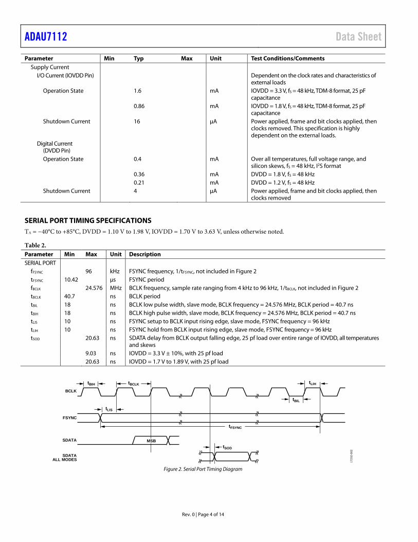
SERIAL PORT TIMING SPECIFICATIONS TA = −40°C to +85°C, DVDD = 1.10 V to 1.98 V, IOVDD = 1.70 V to 3.63 V, unless otherwise noted.
Table 2. Parameter Min Max Unit Description SERIAL PORT
fFSYNC 96 kHz FSYNC frequency, 1/tFSYNC, not included in Figure 2 tFSYNC 10.42 µs FSYNC period fBCLK 24.576 MHz BCLK frequency, sample rate ranging from 4 kHz to 96 kHz, 1/tBCLK, not included in Figure 2 tBCLK 40.7 ns BCLK period tBIL 18 ns BCLK low pulse width, slave mode, BCLK frequency = 24.576 MHz, BCLK period = 40.7 ns tBIH 18 ns BCLK high pulse width, slave mode, BCLK frequency = 24.576 MHz, BCLK period = 40.7 ns tLIS 10 ns FSYNC setup to BCLK input rising edge, slave mode, FSYNC frequency = 96 kHz tLIH 10 ns FSYNC hold from BCLK input rising edge, slave mode, FSYNC frequency = 96 kHz tSOD 20.63 ns SDATA delay from BCLK output falling edge, 25 pf load over entire range of IOVDD, all temperatures
and skews 9.03 ns IOVDD = 3.3 V ± 10%, with 25 pf load 20.63 ns IOVDD = 1.7 V to 1.89 V, with 25 pf load
tBIH tBCLK
tBIL
tLIH
MSB
tLIS
tFSYNC
BCLK
FSYNC
SDATA
SDATAALL MODES
tSOD
1723
2-00
2
Figure 2. Serial Port Timing Diagram
Data Sheet ADAU7112
Rev. 0 | Page 5 of 14
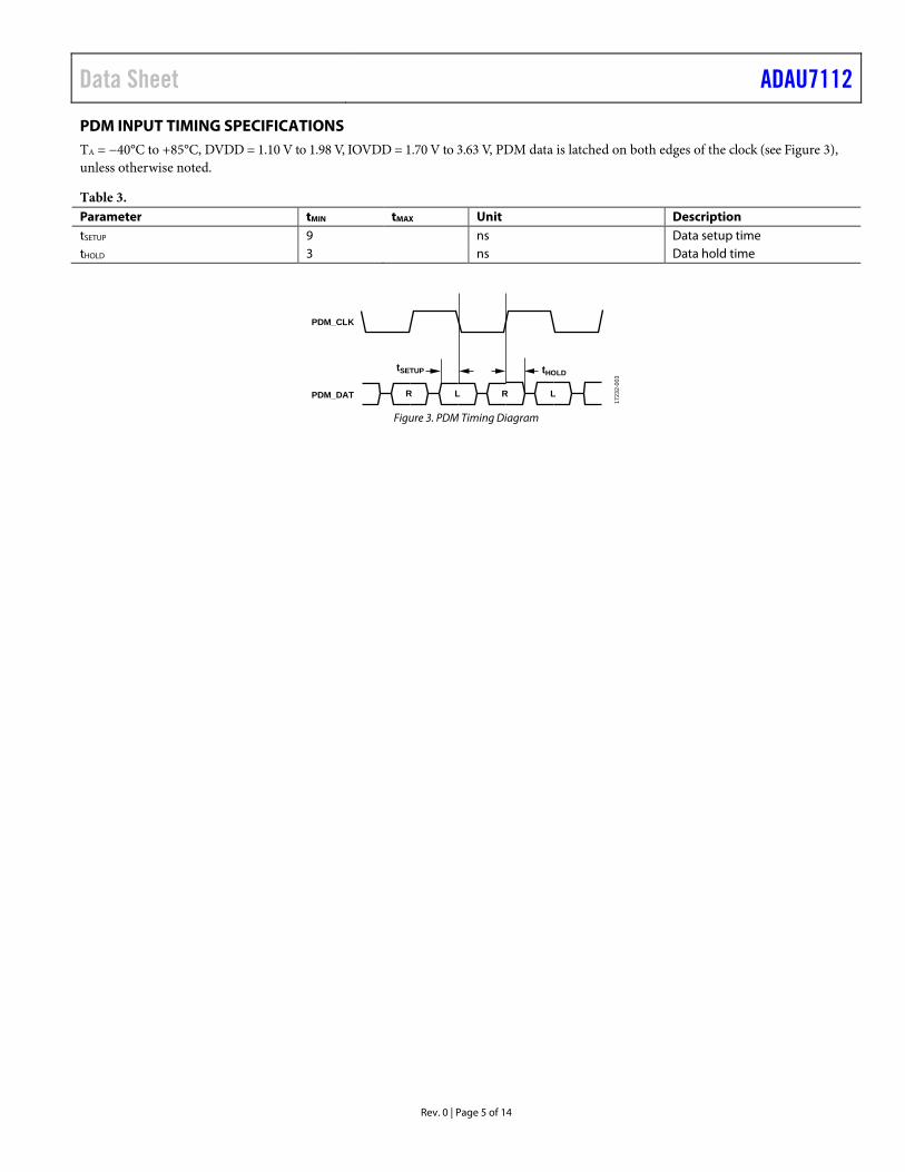
PDM INPUT TIMING SPECIFICATIONS TA = −40°C to +85°C, DVDD = 1.10 V to 1.98 V, IOVDD = 1.70 V to 3.63 V, PDM data is latched on both edges of the clock (see Figure 3), unless otherwise noted.
Table 3. Parameter tMIN tMAX Unit Description tSETUP 9 ns Data setup time tHOLD 3 ns Data hold time
RL
tHOLDtSETUP
PDM_CLK
PDM_DAT R L
1723
2-00
3
Figure 3. PDM Timing Diagram
ADAU7112 Data Sheet
Rev. 0 | Page 6 of 14
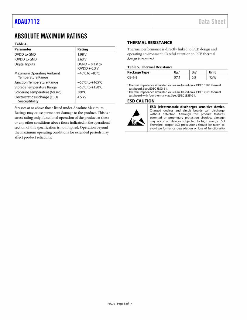
ABSOLUTE MAXIMUM RATINGS Table 4. Parameter Rating DVDD to GND 1.98 V IOVDD to GND 3.63 V Digital Inputs DGND − 0.3 V to
IOVDD + 0.3 V Maximum Operating Ambient
Temperature Range −40°C to +85°C
Junction Temperature Range −65°C to +165°C Storage Temperature Range −65°C to +150°C Soldering Temperature (60 sec) 300°C Electrostatic Discharge (ESD)
Susceptibility 4.5 kV
Stresses at or above those listed under Absolute Maximum Ratings may cause permanent damage to the product. This is a stress rating only; functional operation of the product at these or any other conditions above those indicated in the operational section of this specification is not implied. Operation beyond the maximum operating conditions for extended periods may affect product reliability.
THERMAL RESISTANCE Thermal performance is directly linked to PCB design and operating environment. Careful attention to PCB thermal design is required.
Table 5. Thermal Resistance Package Type θJA
1 θJC2 Unit
CB-9-8 57.1 0.5 °C/W
1 Thermal impedance simulated values are based on a JEDEC 1S0P thermal test board. See JEDEC JESD-51.
2 Thermal impedance simulated values are based on a JEDEC 2S2P thermal test board with four thermal vias. See JEDEC JESD-51.
ESD CAUTION
Data Sheet ADAU7112
Rev. 0 | Page 7 of 14
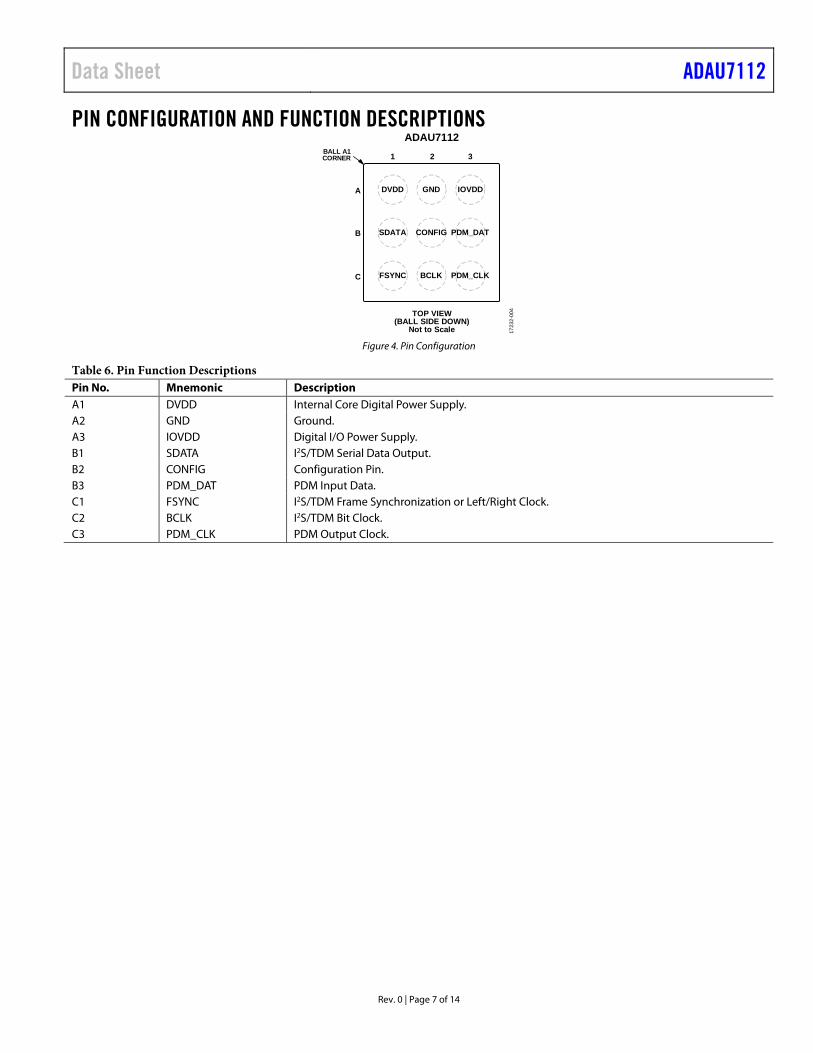
PIN CONFIGURATION AND FUNCTION DESCRIPTIONS
TOP VIEW(BALL SIDE DOWN)
Not to Scale
ADAU7112BALL A1CORNER
A
321
IOVDDGNDDVDD
PDM_DATCONFIGSDATA
PDM_CLKBCLKFSYNC
B
C
1723
2-00
4
Figure 4. Pin Configuration
Table 6. Pin Function Descriptions Pin No. Mnemonic Description A1 DVDD Internal Core Digital Power Supply. A2 GND Ground. A3 IOVDD Digital I/O Power Supply. B1 SDATA I2S/TDM Serial Data Output. B2 CONFIG Configuration Pin. B3 PDM_DAT PDM Input Data. C1 FSYNC I2S/TDM Frame Synchronization or Left/Right Clock. C2 BCLK I2S/TDM Bit Clock. C3 PDM_CLK PDM Output Clock.
ADAU7112 Data Sheet
Rev. 0 | Page 8 of 14
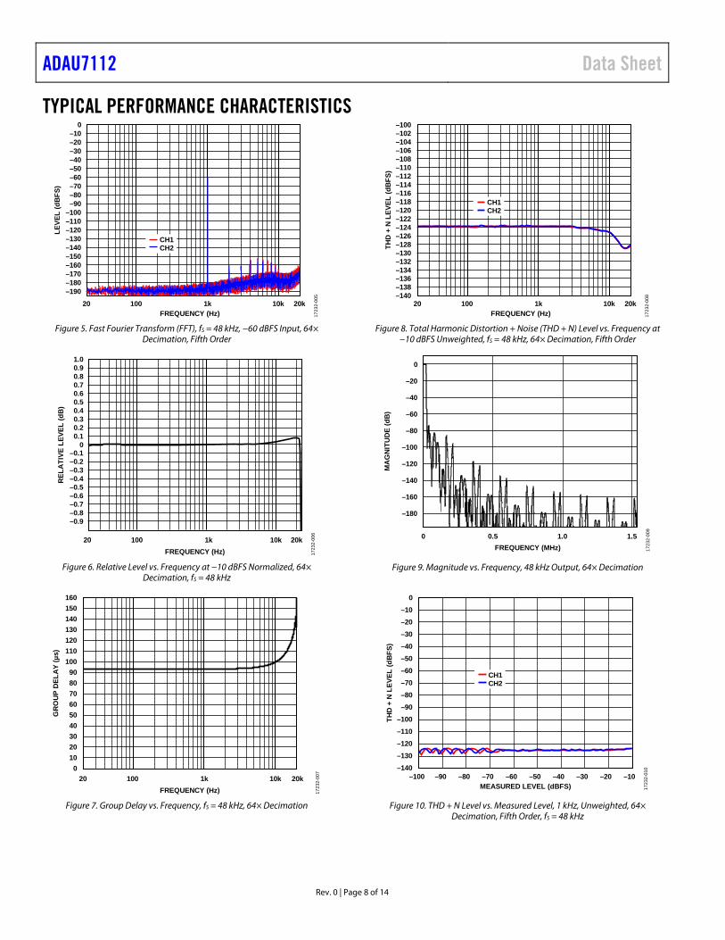
TYPICAL PERFORMANCE CHARACTERISTICS 0
–10–20–30–40–50–60–70–80–90
–100–110–120–130–140–150–160–170–180–190
LEVE
L (d
BFS)
FREQUENCY (Hz)20 100 1k 10k 20k
CH1CH2
1723
2-00
5
Figure 5. Fast Fourier Transform (FFT), fS = 48 kHz, −60 dBFS Input, 64× Decimation, Fifth Order
1.00.90.80.70.60.50.40.30.20.1
–0.1–0.2–0.3–0.4–0.5–0.6–0.7–0.8–0.9
FREQUENCY (Hz)
RELA
TIVE
LEV
EL (d
B)
0
20 100 1k 10k 20k
1723
2-00
6
Figure 6. Relative Level vs. Frequency at −10 dBFS Normalized, 64×
Decimation, fS = 48 kHz
FREQUENCY (Hz)20 100 1k 10k 20k
GRO
UP D
ELAY
(µs)
0102030405060708090
100110120130140150160
1723
2-00
7
Figure 7. Group Delay vs. Frequency, fS = 48 kHz, 64× Decimation
THD
+ N
LEVE
L (d
BFS)
FREQUENCY (Hz)20 100
–100–102–104–106–108–110–112–114–116–118–120–122–124–126–128–130–132–134–136–138–140
1k 10k 20k
CH1CH2
1723
2-00
8
Figure 8. Total Harmonic Distortion + Noise (THD + N) Level vs. Frequency at
−10 dBFS Unweighted, fS = 48 kHz, 64× Decimation, Fifth Order
0
–20
–40
–60
0 0.5FREQUENCY (MHz)
1.0 1.5
MAG
NITU
DE (d
B)
–80
–100
–120
–140
–160
–180
1723
2-00
9
Figure 9. Magnitude vs. Frequency, 48 kHz Output, 64× Decimation
THD
+ N
LEVE
L (d
BFS)
MEASURED LEVEL (dBFS)–100 –90 –80 –70 –60 –50 –40 –30 –20 –10
0–10–20–30–40–50–60–70–80–90
–100–110–120–130–140
CH1CH2
1723
2-01
0
Figure 10. THD + N Level vs. Measured Level, 1 kHz, Unweighted, 64× Decimation, Fifth Order, fS = 48 kHz
Data Sheet ADAU7112
Rev. 0 | Page 9 of 14
THEORY OF OPERATION The ADAU7112 provides up to two channels of decimation from a 1-bit PDM source to a 24-bit PCM audio output. The downsampling ratio is 64 × fS, with fS being the PCM output sampling rate. All channels decimate at the same ratio. The 24-bit downsampled PCM audio is output via standard I2S or TDM format.
The input sources for the ADAU7112 can be any device that has a slave PDM output, such as a digital microphone. The output pins of these microphones can connect directly to the input pins of the ADAU7112.
The PDM_DAT input pin is connected to the data output of the PDM sources. Internally, there are two channels, Channel 0 and Channel 1. The mapping of the PDM_DAT input data to internal channels is shown in Table 7.
Table 7. PDM_DAT to Internal Channel Mapping Input Pin PDM_CLK Edge Internal Channel PDM_DAT Falling 0 Rising 1
POWER-UP AND INITIALIZATION The ADAU7112 requires two power supplies to function: IOVDD and the DVDD. Both power supplies can be applied at the same time. If the power supplies are applied at different times, IOVDD must be applied first and then DVDD can be applied at any point after. There are no timing restrictions.
After the power supplies stabilize, the device initializes and is ready to accept incoming I2S clocks.
After the initialization is complete and I2S clocks are applied, it takes 16 full frame synchronization cycles to begin sending out PDM clocks. When the PDM clocks start, and after another 48 frame synchronization cycles, the PDM data is available on the SDATA pin. These 64 frame sync cycles are listed in Table 1.
CLOCKING After power is applied and the power-up initialization is complete, the device is ready to accept I2S clocks. At this point, it takes 16 full frame synchronization cycles for the device to fully initialize and start sending PDM clocks. If during normal operation the bit clock or frame synchronization is removed, the ADAU7112 PDM_CLK outputs stop immediately and the ADAU7112 automatically enters a low power state. See the Power-Down State section for more details. When the clocks resume, the ADAU7112 relocks to the bit clock and the frame synchronization signals and adjusts the PDM_CLK outputs accordingly. The length of time before the PDM clock outputs resume is 4 frames ± 1 frame to lock to the incoming signal. If the format of the clock signals changes, the ADAU7112 detects this change at the end of the frame and stops the PDM clock outputs. Then, the device reconfigures and resumes sending PDM clocks with no user intervention. Again, this usually takes 4 frames ± 1 frame to lock to the incoming signal.
The ADAU7112 requires a BCLK rate that is a minimum of 64× the frame sync (FSYNC) sample rate. BCLK rates of 128×, 192×, 256×, 384×, and 512× the FSYNC rate are also supported. The ADAU7112 automatically detects the ratio between BCLK and FSYNC and generates a PDM clock output at 64× the FSYNC rate. The minimum sampling rate is 4 kHz, and the maximum sample rate is 96 kHz. The PDM clock range is 256 kHz to 6.144 MHz. Internally, all processing is performed at the PDM_CLK rate.
POWER-DOWN STATE The ADAU7112 can be placed in a power-down state by stopping the frame and bit clocks that are being sent to the device.
To exit power-down mode, resume sending frame and bit clocks to the device.
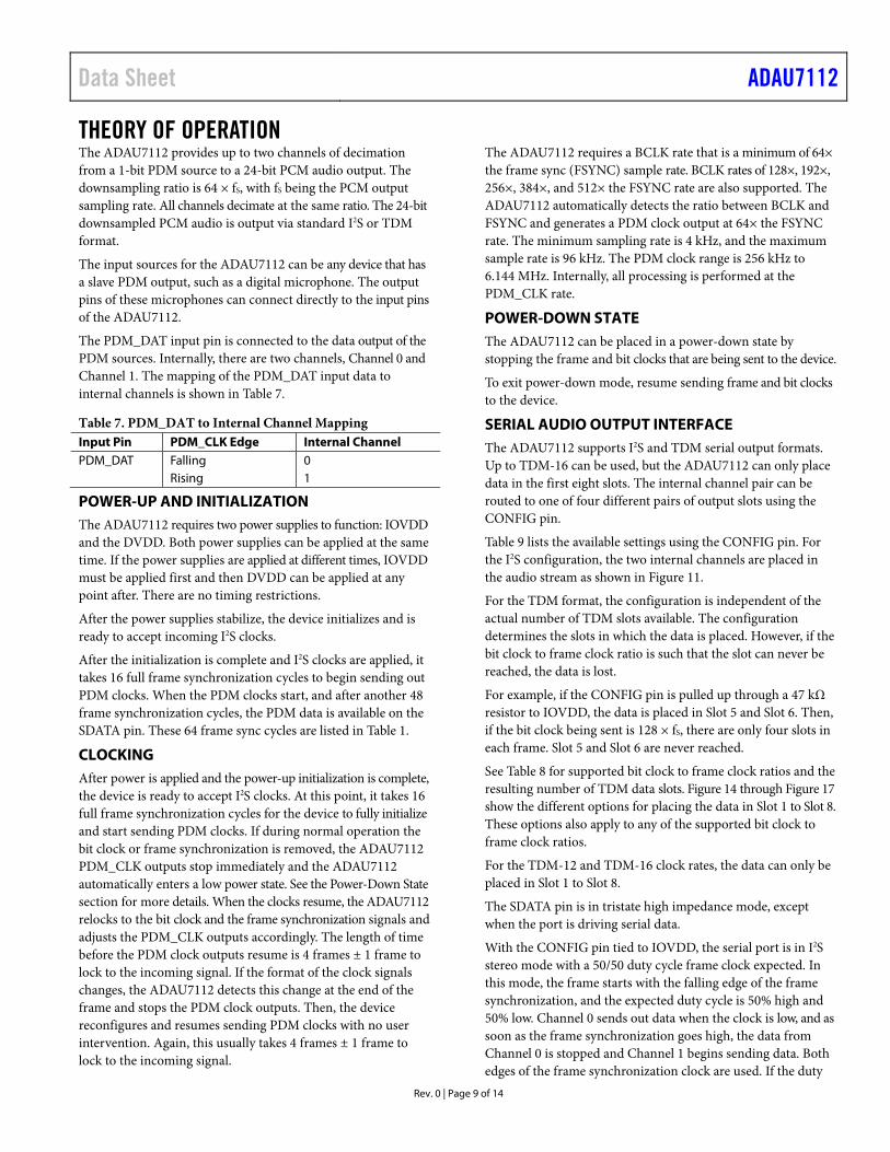
SERIAL AUDIO OUTPUT INTERFACE The ADAU7112 supports I2S and TDM serial output formats. Up to TDM-16 can be used, but the ADAU7112 can only place data in the first eight slots. The internal channel pair can be routed to one of four different pairs of output slots using the CONFIG pin.
Table 9 lists the available settings using the CONFIG pin. For the I2S configuration, the two internal channels are placed in the audio stream as shown in Figure 11.
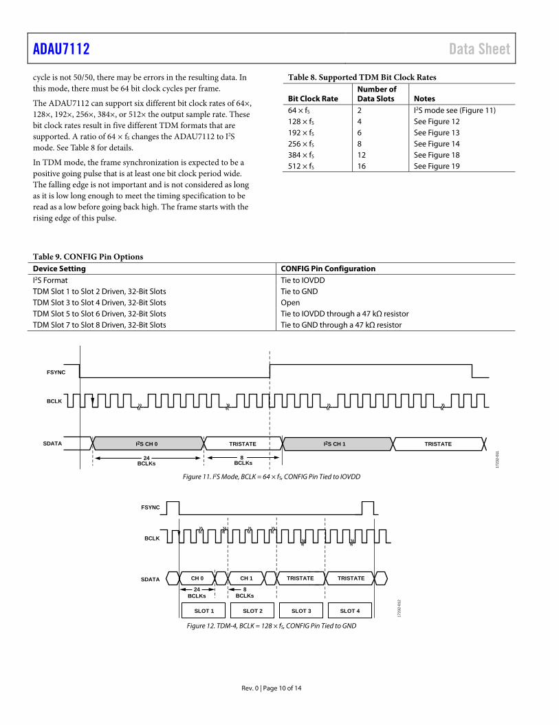
For the TDM format, the configuration is independent of the actual number of TDM slots available. The configuration determines the slots in which the data is placed. However, if the bit clock to frame clock ratio is such that the slot can never be reached, the data is lost.
For example, if the CONFIG pin is pulled up through a 47 kΩ resistor to IOVDD, the data is placed in Slot 5 and Slot 6. Then, if the bit clock being sent is 128 × fS, there are only four slots in each frame. Slot 5 and Slot 6 are never reached.
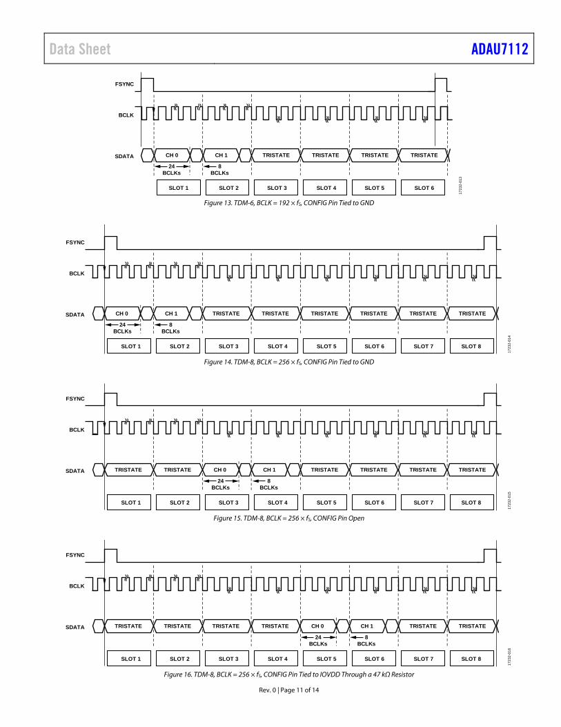
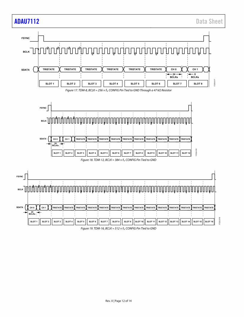
See Table 8 for supported bit clock to frame clock ratios and the resulting number of TDM data slots. Figure 14 through Figure 17 show the different options for placing the data in Slot 1 to Slot 8. These options also apply to any of the supported bit clock to frame clock ratios.
For the TDM-12 and TDM-16 clock rates, the data can only be placed in Slot 1 to Slot 8.
The SDATA pin is in tristate high impedance mode, except when the port is driving serial data.
With the CONFIG pin tied to IOVDD, the serial port is in I2S stereo mode with a 50/50 duty cycle frame clock expected. In this mode, the frame starts with the falling edge of the frame synchronization, and the expected duty cycle is 50% high and 50% low. Channel 0 sends out data when the clock is low, and as soon as the frame synchronization goes high, the data from Channel 0 is stopped and Channel 1 begins sending data. Both edges of the frame synchronization clock are used. If the duty
ADAU7112 Data Sheet
Rev. 0 | Page 10 of 14
cycle is not 50/50, there may be errors in the resulting data. In this mode, there must be 64 bit clock cycles per frame.
The ADAU7112 can support six different bit clock rates of 64×, 128×, 192×, 256×, 384×, or 512× the output sample rate. These bit clock rates result in five different TDM formats that are supported. A ratio of 64 × fS changes the ADAU7112 to I2S mode. See Table 8 for details.
In TDM mode, the frame synchronization is expected to be a positive going pulse that is at least one bit clock period wide. The falling edge is not important and is not considered as long as it is low long enough to meet the timing specification to be read as a low before going back high. The frame starts with the rising edge of this pulse.
Table 8. Supported TDM Bit Clock Rates
Bit Clock Rate Number of Data Slots Notes
64 × fS 2 I2S mode see (Figure 11) 128 × fS 4 See Figure 12 192 × fS 6 See Figure 13 256 × fS 8 See Figure 14 384 × fS 12 See Figure 18 512 × fS 16 See Figure 19
Table 9. CONFIG Pin Options Device Setting CONFIG Pin Configuration I2S Format Tie to IOVDD TDM Slot 1 to Slot 2 Driven, 32-Bit Slots Tie to GND TDM Slot 3 to Slot 4 Driven, 32-Bit Slots Open TDM Slot 5 to Slot 6 Driven, 32-Bit Slots Tie to IOVDD through a 47 kΩ resistor TDM Slot 7 to Slot 8 Driven, 32-Bit Slots Tie to GND through a 47 kΩ resistor
FSYNC
BCLK
SDATA I2S CH 0 I2S CH 1
24BCLKs
TRISTATE TRISTATE
8BCLKs
1723
2-01
1
Figure 11. I2S Mode, BCLK = 64 × fS, CONFIG Pin Tied to IOVDD
SLOT 2SLOT 1
FSYNC
BCLK
SDATA
24 8BCLKsBCLKs
CH 1CH 0
SLOT 3 SLOT 4
TRISTATE TRISTATE
1723
2-01
2
Figure 12. TDM-4, BCLK = 128 × fS, CONFIG Pin Tied to GND
Data Sheet ADAU7112
Rev. 0 | Page 11 of 14
SLOT 2
FSYNC
BCLK
SDATA
24 8BCLKsBCLKs
CH 1CH 0
SLOT 3 SLOT 4 SLOT 5 SLOT 6SLOT 1
TRISTATE TRISTATE TRISTATE TRISTATE
1723
2-01
3
Figure 13. TDM-6, BCLK = 192 × fS, CONFIG Pin Tied to GND
SLOT 1
FSYNC
BCLK
SDATA
24BCLKs
CH 1CH 0
SLOT 2 SLOT 3 SLOT 4 SLOT 5 SLOT 6 SLOT 7 SLOT 8
TRISTATE TRISTATE TRISTATE TRISTATE TRISTATE TRISTATE
8BCLKs
1723
2-01
4
Figure 14. TDM-8, BCLK = 256 × fS, CONFIG Pin Tied to GND
SLOT 1
FSYNC
BCLK
SDATA
SLOT 2 SLOT 3 SLOT 4 SLOT 5 SLOT 6 SLOT 7 SLOT 8
TRISTATE TRISTATE TRISTATE TRISTATE TRISTATE TRISTATECH 1
8BCLKs
24BCLKs
CH 0
1723
2-01
5
Figure 15. TDM-8, BCLK = 256 × fS, CONFIG Pin Open
SLOT 1
FSYNC
BCLK
SDATA
SLOT 2 SLOT 3 SLOT 4 SLOT 5 SLOT 6 SLOT 7 SLOT 8
TRISTATE TRISTATE TRISTATE TRISTATECH 1
8BCLKs
24BCLKs
CH 0TRISTATE TRISTATE
1723
2-01
6
Figure 16. TDM-8, BCLK = 256 × fS, CONFIG Pin Tied to IOVDD Through a 47 kΩ Resistor
ADAU7112 Data Sheet
Rev. 0 | Page 12 of 14
SLOT 1
FSYNC
BCLK
SDATA
SLOT 2 SLOT 3 SLOT 4 SLOT 5 SLOT 6 SLOT 7 SLOT 8
TRISTATE TRISTATE CH 1
8BCLKs
24BCLKs
CH 0TRISTATE TRISTATE TRISTATE TRISTATE
17232-017
Figure 17. TDM-8, BCLK = 256 × fS, CONFIG Pin Tied to GND Through a 47 kΩ Resistor
FSYNC
BCLK
SDATA
24BCLKs
CH 1CH 0
SLOT 1 SLOT 2 SLOT 3 SLOT 4 SLOT 5 SLOT 6 SLOT 7 SLOT 8 SLOT 9 SLOT 10 SLOT 11 SLOT 12
TRISTATETRISTATETRISTATETRISTATETRISTATETRISTATETRISTATE TRISTATE TRISTATE TRISTATE
17232-018
Figure 18. TDM-12, BCLK = 384 × fS, CONFIG Pin Tied to GND
FSYNC
BCLK
SDATA
24BCLKs
CH 1CH 0
SLOT 1 SLOT 2 SLOT 3 SLOT 4 SLOT 5 SLOT 6 SLOT 7 SLOT 8 SLOT 9 SLOT 10 SLOT 11
TRISTATETRISTATETRISTATETRISTATETRISTATETRISTATETRISTATE TRISTATE TRISTATE
SLOT 12
TRISTATE
SLOT 13
TRISTATE
SLOT 14
TRISTATE
SLOT 15
TRISTATE
SLOT 16
TRISTATE
17232-019
Figure 19. TDM-16, BCLK = 512 × fS, CONFIG Pin Tied to GND
Data Sheet ADAU7112
Rev. 0 | Page 13 of 14
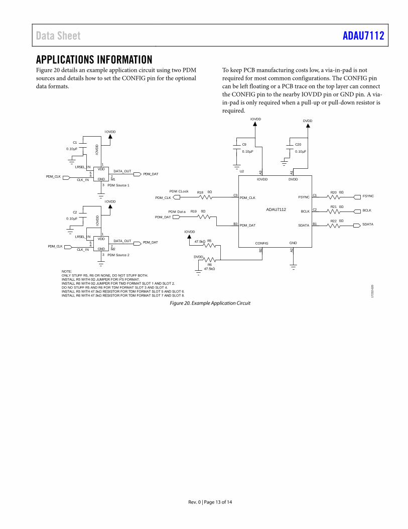
APPLICATIONS INFORMATION Figure 20 details an example application circuit using two PDM sources and details how to set the CONFIG pin for the optional data formats.
To keep PCB manufacturing costs low, a via-in-pad is not required for most common configurations. The CONFIG pin can be left floating or a PCB trace on the top layer can connect the CONFIG pin to the nearby IOVDD pin or GND pin. A via-in-pad is only required when a pull-up or pull-down resistor is required.
PDM CLock
PDM Dat a
C9
0.10µF
R547.5kΩ
47.5kΩR6
C20
0.10µF
R18 0Ω
R19 0Ω
R20 0Ω
0Ω
0Ω
R21
R22
A1A2
GND
A3
B1
B2
CONFIG
B3
C1
C2
C3
U25
LRSEL_IN
4CLK_IN
2DATA_OUT
3
GND
1VDD
M1
PDM Source 1
5
LRSEL_IN
4CLK_IN
2DATA_OUT
3
GND
1VDD
M2
PDM Source 2
C1
0.10µF
C2
0.10µF
IOVDD
IOVDD
IOVDD
DVDD
DVDD
DVDD
FSYNC
BCLK
SDATA
FSYNC
BCLK
SDATA
IOVDD
IOVD
D
IOVDD
IOVD
D
PDM_DAT
PDM_DAT
PDM_CLK
PDM_CLK
PDM_CLK
PDM_DAT
PDM_CLK
PDM_DAT
ADAU7112
NOTE:ONLY STUFF R5, R6 OR NONE, DO NOT STUFF BOTH.INSTALL R5 WITH 0Ω JUMPER FOR I2S FORMAT.INSTALL R6 WITH 0Ω JUMPER FOR TMD FORMAT SLOT 1 AND SLOT 2.DO NO STUFF R5 AND R6 FOR TDM FORMAT SLOT 3 AND SLOT 4.INSTALL R5 WITH 47.5kΩ RESISTOR FOR TDM FORMAT SLOT 5 AND SLOT 6.INSTALL R6 WITH 47.5kΩ RESISTOR FOR TDM FORMAT SLOT 7 AND SLOT 8. 17
232-
020
Figure 20. Example Application Circuit
ADAU7112 Data Sheet
Rev. 0 | Page 14 of 14
OUTLINE DIMENSIONS
A
B
C
1.3001.2601.220
123
0.3000.2600.220
0.80REF
0.40BSC
0.2300.2000.170
0.5600.5000.440
COPLANARITY0.05
PKG
-005
978
BOTTOM VIEW(BALL SIDE UP)
TOP VIEW(BALL SIDE DOWN)
SIDE VIEW
06-1
2-20
18-A
SEATINGPLANE
IDENTIFIER
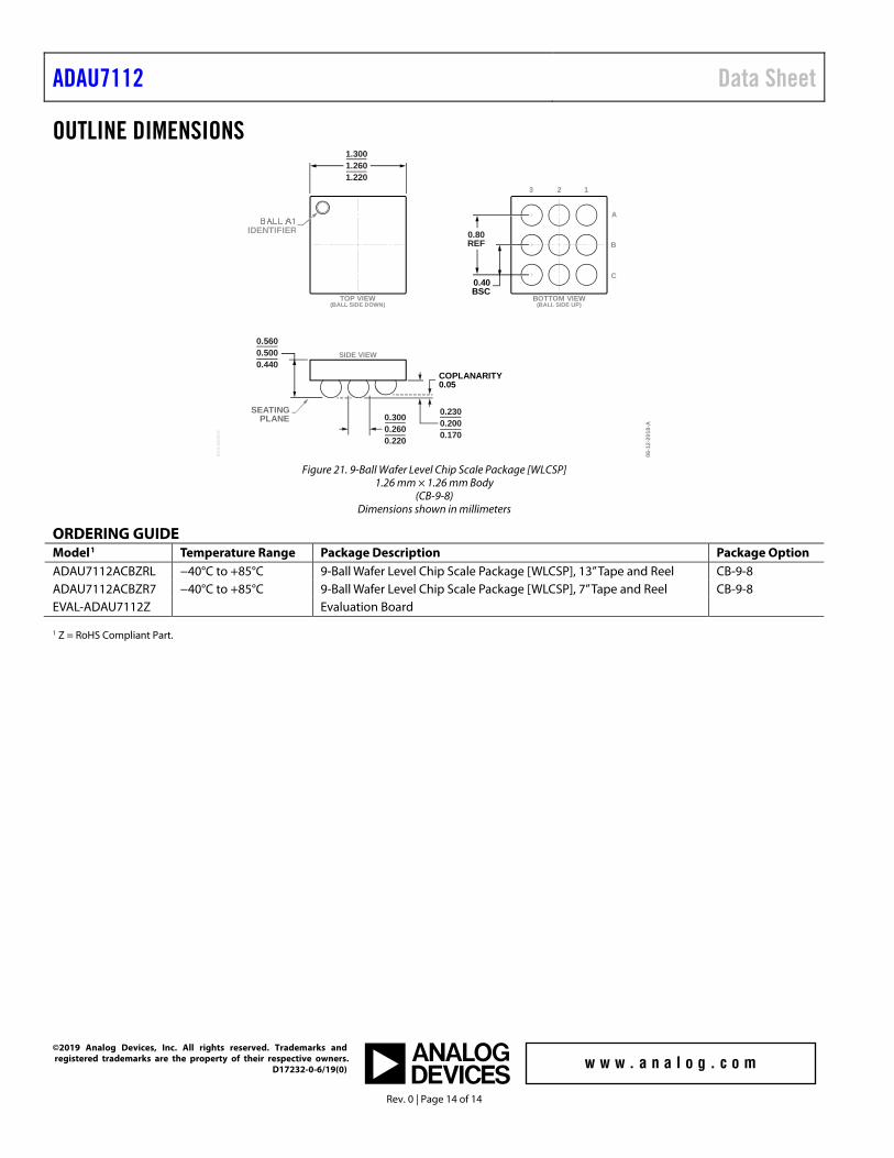
Figure 21. 9-Ball Wafer Level Chip Scale Package [WLCSP]
1.26 mm × 1.26 mm Body (CB-9-8)
Dimensions shown in millimeters
ORDERING GUIDE Model1 Temperature Range Package Description Package Option ADAU7112ACBZRL −40°C to +85°C 9-Ball Wafer Level Chip Scale Package [WLCSP], 13” Tape and Reel CB-9-8 ADAU7112ACBZR7 −40°C to +85°C 9-Ball Wafer Level Chip Scale Package [WLCSP], 7” Tape and Reel CB-9-8 EVAL-ADAU7112Z Evaluation Board 1 Z = RoHS Compliant Part.
©2019 Analog Devices, Inc. All rights reserved. Trademarks and registered trademarks are the property of their respective owners. D17232-0-6/19(0)


