Embed Size (px)
Citation preview

e-learning
Electricity & Electronics
Control & Instrumentation
Process Control
Mechatronics
Telecommunications
Electrical Power & Machines
Test & Measurement
Amplifiers and Electronic Circuit Applications
EEC473-4
Feedback Instruments Ltd, Park Road, Crowborough, E. Sussex, TN6 2QR, UK.
Telephone: +44 (0) 1892 653322, Fax: +44 (0) 1892 663719. email: [email protected] website: http://www.fbk.com
Manual: EEC473-4 Ed09 122005 Printed in England by Fl Ltd, Crowborough
Feedback Part No. 1160–EEC473-4

Notes
AMPLIFIERS AND ELECTRONIC CIRCUIT APPLICATIONS PREFACE
EEC473-4 i
THE HEALTH AND SAFETY AT WORK ACT 1974 We are required under the Health and Safety at Work Act 1974, to make available to users of this equipment certain information regarding its safe use. The equipment, when used in normal or prescribed applications within the parameters set for its mechanical and electrical performance, should not cause any danger or hazard to health or safety if normal engineering practices are observed and they are used in accordance with the instructions supplied. If, in specific cases, circumstances exist in which a potential hazard may be brought about by careless or improper use, these will be pointed out and the necessary precautions emphasised. While we provide the fullest possible user information relating to the proper use of this equipment, if there is any doubt whatsoever about any aspect, the user should contact the Product Safety Officer at Feedback Instruments Limited, Crowborough. This equipment should not be used by inexperienced users unless they are under supervision. We are required by European Directives to indicate on our equipment panels certain areas and warnings that require attention by the user. These have been indicated in the specified way by yellow labels with black printing, the meaning of any labels that may be fixed to the instrument are shown below:
CAUTION -
RISK OF DANGER
CAUTION -
RISK OF ELECTRIC SHOCK
CAUTION -
ELECTROSTATIC SENSITIVE DEVICE
Refer to accompanying documents
PRODUCT IMPROVEMENTS We maintain a policy of continuous product improvement by incorporating the latest developments and components into our equipment, even up to the time of dispatch. All major changes are incorporated into up-dated editions of our manuals and this manual was believed to be correct at the time of printing. However, some product changes which do not affect the instructional capability of the equipment, may not be included until it is necessary to incorporate other significant changes.
COMPONENT REPLACEMENT Where components are of a ‘Safety Critical’ nature, i.e. all components involved with the supply or carrying of voltages at supply potential or higher, these must be replaced with components of equal international safety approval in order to maintain full equipment safety. In order to maintain compliance with international directives, all replacement components should be identical to those originally supplied. Any component may be ordered direct from Feedback or its agents by quoting the following information:
1. Equipment type 3. Component reference
2. Component value 4. Equipment serial number
Components can often be replaced by alternatives available locally, however we cannot therefore guarantee continued performance either to published specification or compliance with international standards.
AMPLIFIERS AND ELECTRONIC CIRCUIT APPLICATIONS PREFACE
EEC473-4 ii
OPERATING CONDITIONS
This equipment is designed to operate under the following conditions:
Operating Temperature 10°C to 40°C (50°F to 104°F)
Humidity 10% to 90% (non-condensing)
DECLARATION CONCERNING ELECTROMAGNETIC COMPATIBILITY Should this equipment be used outside the classroom, laboratory study area or similar such place for which it is designed and sold then Feedback Instruments Ltd hereby states that conformity with the protection requirements of the European Community Electromagnetic Compatibility Directive (89/336/EEC) may be invalidated and could lead to prosecution. This equipment, when operated in accordance with the supplied documentation, does not cause electromagnetic disturbance outside its immediate electromagnetic environment.
COPYRIGHT NOTICE
© Feedback Instruments Limited All rights reserved. No part of this publication may be reproduced, stored in a retrieval system, or transmitted, in any form or by any means, electronic, mechanical, photocopying, recording or otherwise, without the prior permission of Feedback Instruments Limited.
ACKNOWLEDGEMENTS
Feedback Instruments Ltd acknowledge all trademarks. IBM, IBM - PC are registered trademarks of International Business Machines. MICROSOFT, WINDOWS 95, WINDOWS 98, WINDOWS 2000, WINDOWS ME, WINDOWS NT, WINDOWS XP and Internet Explorer are registered trademarks of Microsoft Corporation.
WARNING:
This equipment must not be used in conditions of condensing humidity.
AMPLIFIERS AND ELECTRONIC CIRCUIT APPLICATIONS Contents
EEC473-4 TOC-1
TABLE OF CONTENTS INTRODUCTION Component Content
Component Identification
Electronic Systems
Familiarisation Exercise
SECTION 1 AMPLIFIERS
1-1. Using Electronic Amplifiers
1-2. Gain
1-3. Distortion
1-4. Negative Feedback
1-5. Frequency Response
1-6. The ac Amplifier
1-7. Power Amplifiers
1-8. Passive Attenuators
1-9. The Operational Amplifier
1-10. The Operational Amplifier Applications
SECTION 2 OSCILLATORS
2-11. The Phase-Shift Oscillator
2-12. The Astable Multivibrator and its Application
2-13. A Unijunction Pulse Generator and its Application
2-14. Timer Circuits SECTION 3 CONTROL – Applications
3-15. A Light-operated Alarm
3-16. A Delay Circuit
3-17. A Light-operated Flasher
3-18. A Temperature-operated Switch
3-19. The Schmitt Trigger
3-20. A Voltage Regulator
AMPLIFIERS AND ELECTRONIC CIRCUIT APPLICATIONS Contents
EEC473-4 TOC-2
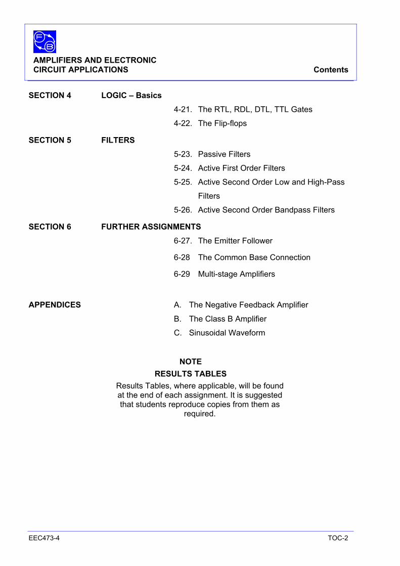
SECTION 4 LOGIC – Basics
4-21. The RTL, RDL, DTL, TTL Gates
4-22. The Flip-flops
SECTION 5 FILTERS
5-23. Passive Filters
5-24. Active First Order Filters
5-25. Active Second Order Low and High-Pass
Filters
5-26. Active Second Order Bandpass Filters
SECTION 6 FURTHER ASSIGNMENTS
6-27. The Emitter Follower
6-28 The Common Base Connection
6-29 Multi-stage Amplifiers
APPENDICES A. The Negative Feedback Amplifier
B. The Class B Amplifier
C. Sinusoidal Waveform
NOTE
RESULTS TABLES Results Tables, where applicable, will be found at the end of each assignment. It is suggested that students reproduce copies from them as
required.
AMPLIFIERS AND ELECTRONIC CIRCUIT APPLICATIONS Introduction
EEC 473-4 Intro-1
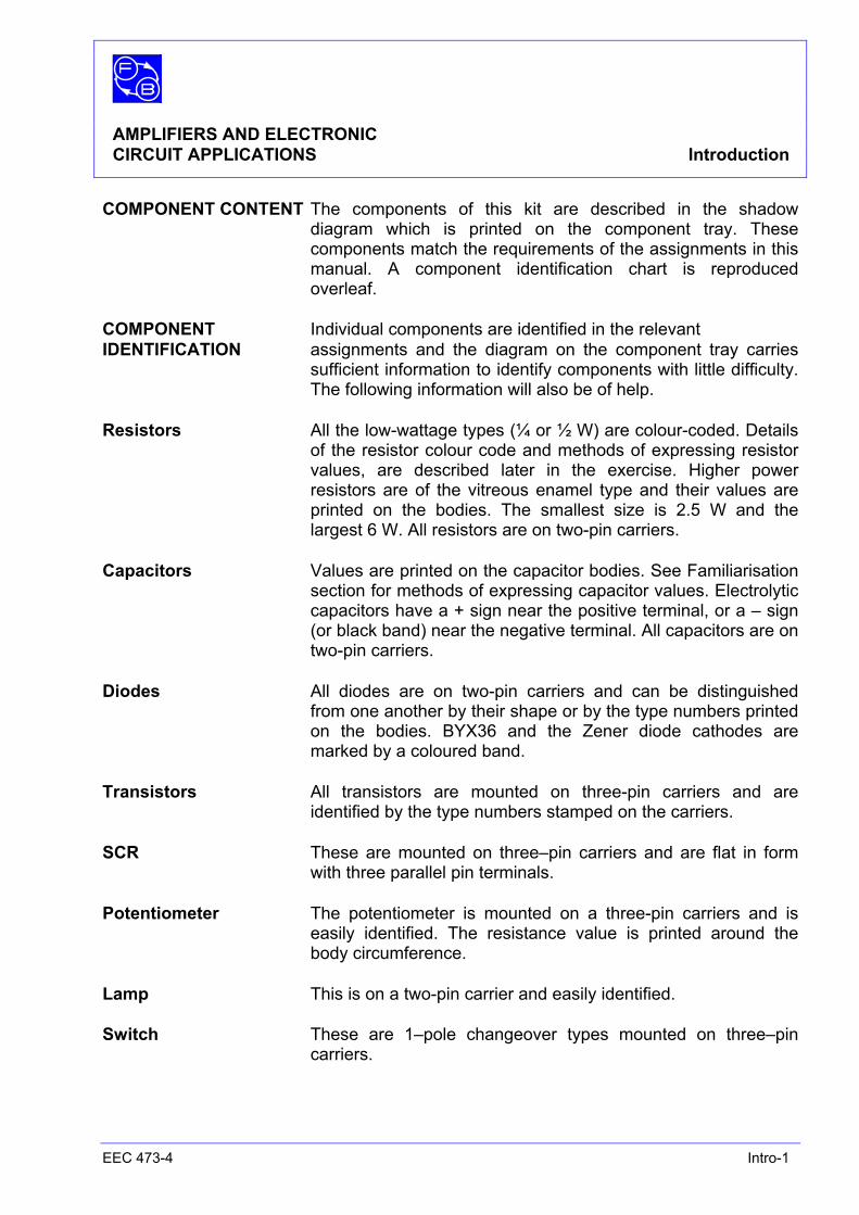
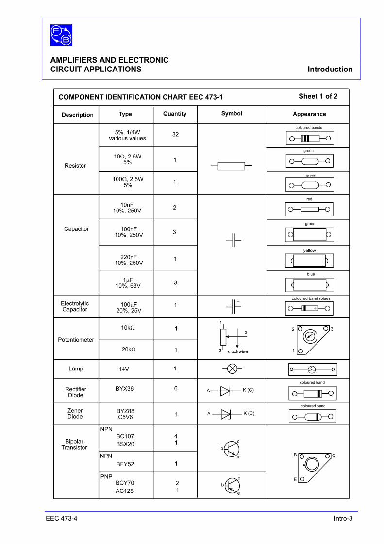
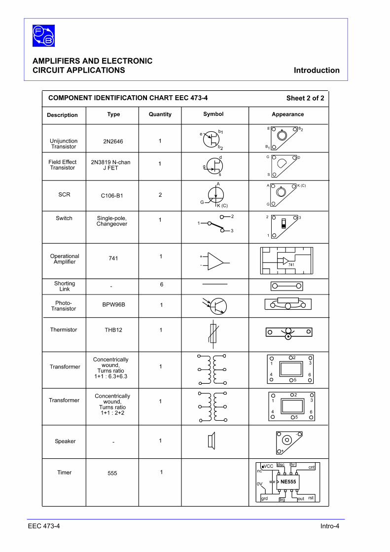
COMPONENT CONTENT The components of this kit are described in the shadow diagram which is printed on the component tray. These components match the requirements of the assignments in this manual. A component identification chart is reproduced overleaf.
COMPONENT Individual components are identified in the relevant IDENTIFICATION assignments and the diagram on the component tray carries
sufficient information to identify components with little difficulty. The following information will also be of help.
Resistors All the low-wattage types (¼ or ½ W) are colour-coded. Details
of the resistor colour code and methods of expressing resistor values, are described later in the exercise. Higher power resistors are of the vitreous enamel type and their values are printed on the bodies. The smallest size is 2.5 W and the largest 6 W. All resistors are on two-pin carriers.
Capacitors Values are printed on the capacitor bodies. See Familiarisation
section for methods of expressing capacitor values. Electrolytic capacitors have a + sign near the positive terminal, or a – sign (or black band) near the negative terminal. All capacitors are on two-pin carriers.
Diodes All diodes are on two-pin carriers and can be distinguished
from one another by their shape or by the type numbers printed on the bodies. BYX36 and the Zener diode cathodes are marked by a coloured band.
Transistors All transistors are mounted on three-pin carriers and are
identified by the type numbers stamped on the carriers. SCR These are mounted on three–pin carriers and are flat in form
with three parallel pin terminals. Potentiometer The potentiometer is mounted on a three-pin carriers and is
easily identified. The resistance value is printed around the body circumference.
Lamp This is on a two-pin carrier and easily identified. Switch These are 1–pole changeover types mounted on three–pin
carriers.
AMPLIFIERS AND ELECTRONIC CIRCUIT APPLICATIONS Introduction
EEC 473-4 Intro-2
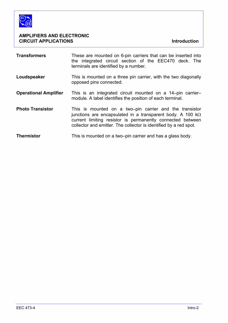
Transformers These are mounted on 6-pin carriers that can be inserted into the integrated circuit section of the EEC470 deck. The terminals are identified by a number.
Loudspeaker This is mounted on a three pin carrier, with the two diagonally
opposed pins connected. Operational Amplifier This is an integrated circuit mounted on a 14–pin carrier–
module. A label identifies the position of each terminal. Photo Transistor This is mounted on a two–pin carrier and the transistor
junctions are encapsulated in a transparent body. A 100 kΩ current limiting resistor is permanently connected between collector and emitter. The collector is identified by a red spot.
Thermistor This is mounted on a two–pin carrier and has a glass body.
AMPLIFIERS AND ELECTRONIC CIRCUIT APPLICATIONS Introduction
EEC 473-4 Intro-3
AMPLIFIERS AND ELECTRONIC CIRCUIT APPLICATIONS Introduction
EEC 473-4 Intro-4
AMPLIFIERS AND ELECTRONIC CIRCUIT APPLICATIONS Introduction
EEC 473-4 Intro-5
ELECTRONIC SYSTEMS EEC473-4 is designed to apply to electronic systems, the
principles learnt in EEC 471-2 – Basic Electronics. The 'systems' approach to engineering is most important and enables complicated processes to be created from basic building blocks. Thus once a system is broken down into its constituent parts, the operation of that part can be understood, and facilitate, for example, its repair without the necessity to understand the operation of the whole system. For instance, a voltage comparator may be included as a tiny part of many different systems, but its function will always be the same (i.e. to compare voltage levels), and once its operation is understood in one system that operation is easy to see in any other system. It is therefore most important to view an electronic circuit, not as a collection of individual transistors, resistors, capacitors, etc but as a collection of interconnected building blocks. In EEC473-4 the individual components will be connected into blocks and their operation, function and performance described.
An electronics system consists of three main parts:
1. A sensing device, called a transducer for converting a quantity into an electric current.
2. A processor which decides what is to be done by using the information from the transducer and converting the required action into a signal which can be accepted by an actuator.
3. An actuator which causes the desired effect to take place.
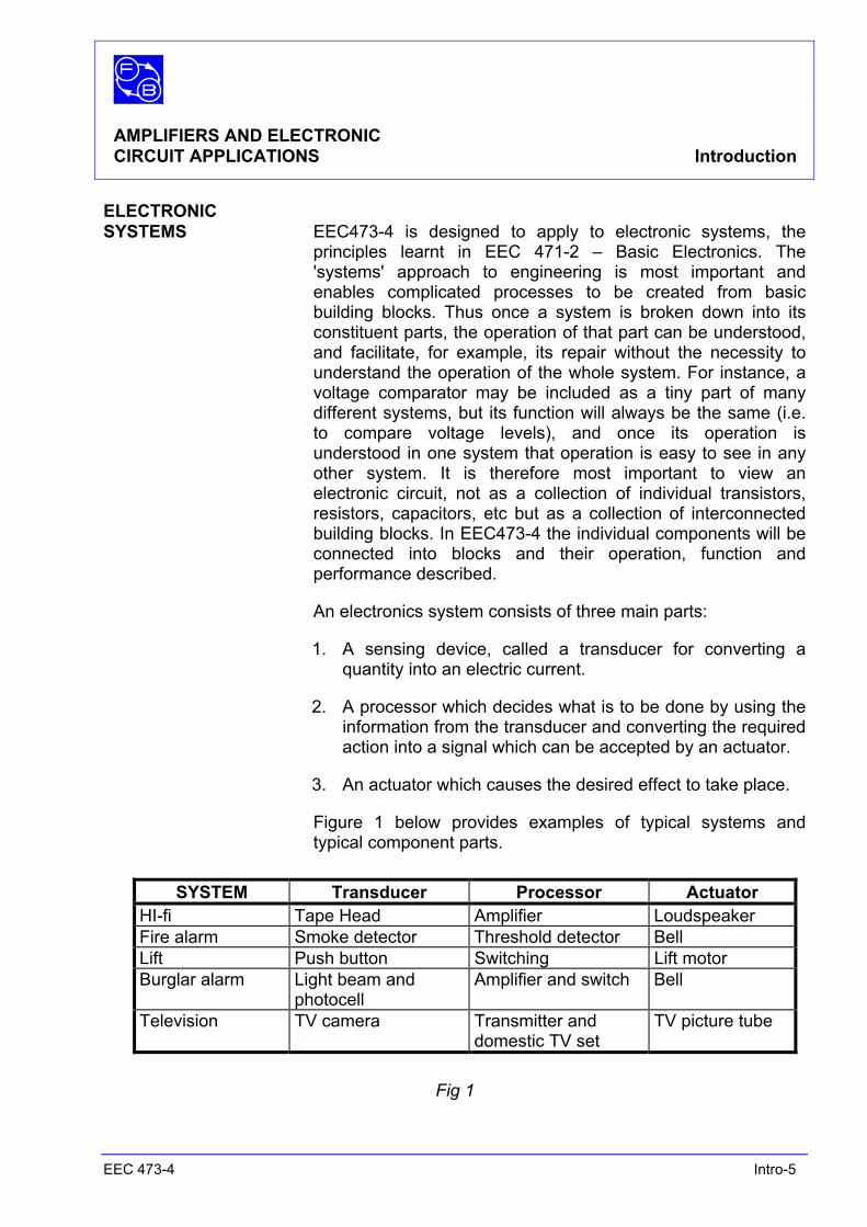
Figure 1 below provides examples of typical systems and typical component parts.
SYSTEM Transducer Processor Actuator HI-fi Tape Head Amplifier Loudspeaker Fire alarm Smoke detector Threshold detector Bell Lift Push button Switching Lift motor Burglar alarm Light beam and
photocell Amplifier and switch Bell
Television TV camera Transmitter and domestic TV set
TV picture tube
Fig 1
AMPLIFIERS AND ELECTRONIC CIRCUIT APPLICATIONS Introduction
EEC 473-4 Intro-6
Transducers There are two types of transducer which have not been described in the previous kit. They are both semiconductor devices but the material from which they are made is different from that used for transistors and diodes. They are:
1. The Thermistor
This is a two-terminal device, the resistance of which changes with temperature. Different types of thermistor change in different directions. They are used to measure temperature.
2. The Photo Conductive Cell
This is also a two-terminal device and has a window through which light can pass. The higher the level of incident light the lower the resistance becomes. It is used to measure light intensity.
Processors In this kit we will deal mainly with the processor part of the system with some reference to certain types of transducer where the type of transducer places certain constraints on the processor.
Amplifiers A visit to a disco is sufficient to explain the purpose of amplifiers. The group who recorded the music made only a fraction of the sound heard coming from the loudspeakers. If you try placing your ear very close to an electric guitar, you will hear only a small sound. It is the electronic amplifier that turns this small noise into the body-vibrating sound coming out of the loudspeakers.
In this kit you will carry out a series of experiments that will give you a broad grasp of the main types of amplifier, the elements from which they are formed, and how to deal with the problems that can occur due to malfunction or ageing. It will help you to understand the electronic amplifier if we go back to the application of the first electric circuits.
Wheatstone and Cook designed the first electric telegraph in 1837, using the ideas of Morse in sending messages composed of short and long time signals. Within a few years electric telegraph networks were established that could traverse continents.
AMPLIFIERS AND ELECTRONIC CIRCUIT APPLICATIONS Introduction
EEC 473-4 Intro-7
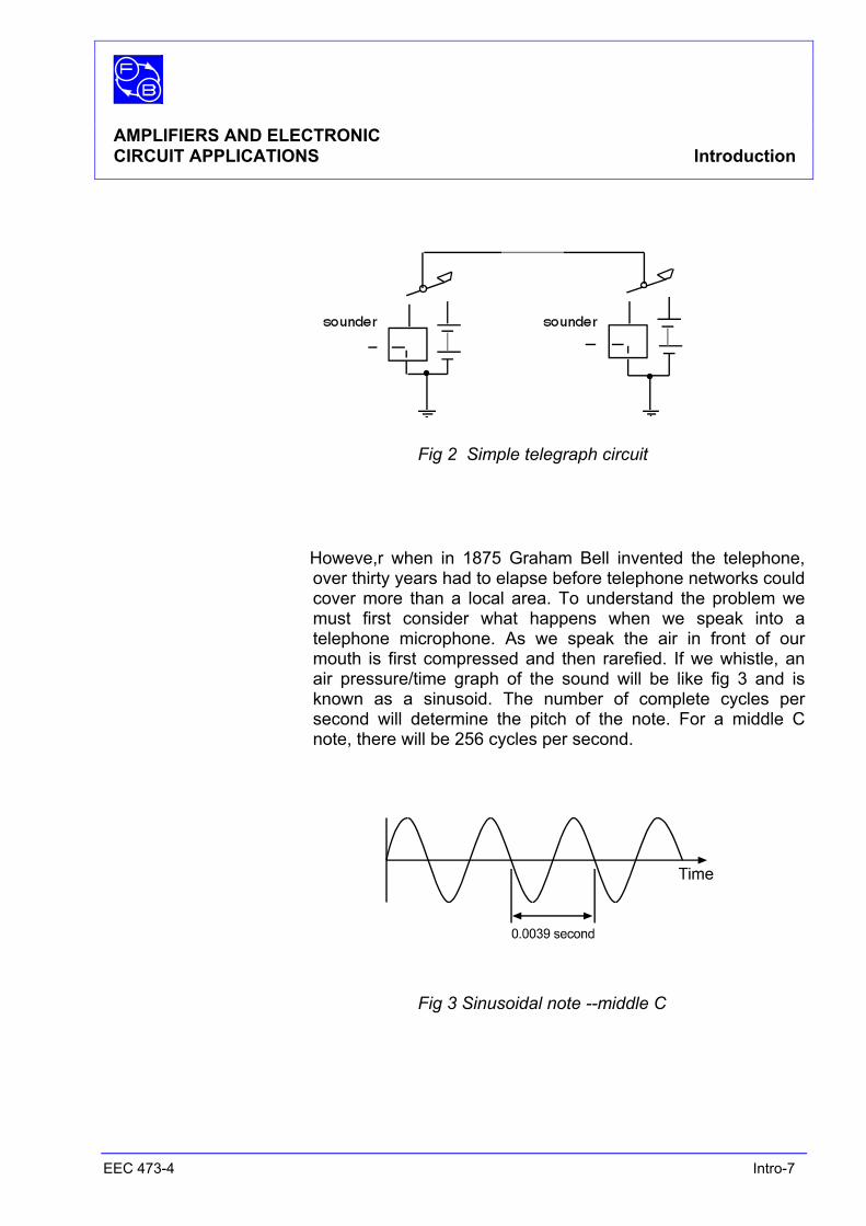
Fig 2 Simple telegraph circuit
Howeve,r when in 1875 Graham Bell invented the telephone, over thirty years had to elapse before telephone networks could cover more than a local area. To understand the problem we must first consider what happens when we speak into a telephone microphone. As we speak the air in front of our mouth is first compressed and then rarefied. If we whistle, an air pressure/time graph of the sound will be like fig 3 and is known as a sinusoid. The number of complete cycles per second will determine the pitch of the note. For a middle C note, there will be 256 cycles per second.
Fig 3 Sinusoidal note --middle C
AMPLIFIERS AND ELECTRONIC CIRCUIT APPLICATIONS Introduction
EEC 473-4 Intro-8
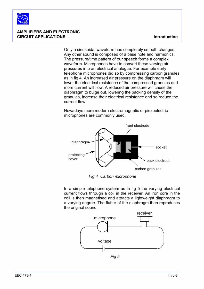
Only a sinusoidal waveform has completely smooth changes. Any other sound is composed of a base note and harmonics. The pressure/time pattern of our speech forms a complex waveform. Microphones have to convert these varying air pressures into an electrical analogue. For example early telephone microphones did so by compressing carbon granules as in fig 4. An increased air pressure on the diaphragm will lower the electrical resistance of the compressed granules and more current will flow. A reduced air pressure will cause the diaphragm to bulge out, lowering the packing density of the granules, increase their electrical resistance and so reduce the current flow.
Nowadays more modern electromagnetic or piezoelectric microphones are commonly used.
front electrode
socket
back electrode
carbon granules
diaphragm
protecting cover
Fig 4 Carbon microphone
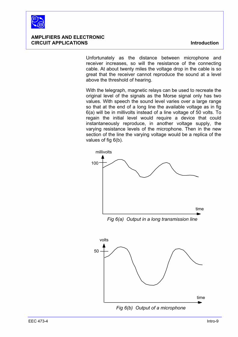
In a simple telephone system as in fig 5 the varying electrical
current flows through a coil in the receiver. An iron core in the coil is then magnetised and attracts a lightweight diaphragm to a varying degree. The flutter of the diaphragm then reproduces the original sound.
microphonereceiver
voltage
Fig 5
AMPLIFIERS AND ELECTRONIC CIRCUIT APPLICATIONS Introduction
EEC 473-4 Intro-9
Unfortunately as the distance between microphone and receiver increases, so will the resistance of the connecting cable. At about twenty miles the voltage drop in the cable is so great that the receiver cannot reproduce the sound at a level above the threshold of hearing.
With the telegraph, magnetic relays can be used to recreate the original level of the signals as the Morse signal only has two values. With speech the sound level varies over a large range so that at the end of a long line the available voltage as in fig 6(a) will be in millivolts instead of a line voltage of 50 volts. To regain the initial level would require a device that could instantaneously reproduce, in another voltage supply, the varying resistance levels of the microphone. Then in the new section of the line the varying voltage would be a replica of the values of fig 6(b).
millivolts
time
100
Fig 6(a) Output in a long transmission line
volts
time
50
Fig 6(b) Output of a microphone
AMPLIFIERS AND ELECTRONIC CIRCUIT APPLICATIONS Introduction
EEC 473-4 Intro-10
Amplifier Devices The invention in 1906 by Lee de Forest of the thermionic triode valve produced such a device. The triode allowed the signal to set up an electrostatic field to control the flow of electrons in a vacuum. By this means a small change in voltage at the triode input produced a large change in current in its output. Also the triode could operate at various levels of input signal. In the fields of telecommunications, radio and industry the triode, and its derivatives, was the device used whenever there was a need for a signal to be amplified. Today the thermionic amplifier has been superseded by semiconductor amplifiers. Although the principle of semiconduction was introduced in the 1930s it was not until 1948 that Shockley produced the first practical transistor in which a current controlled the electron flow and which became known as the bipolar transistor.
AMPLIFIERS AND ELECTRONIC CIRCUIT APPLICATIONS Familiarisation Exercise
EEC 473-4 Familiarisation-1
OBJECTIVES 1. To become familiar with the EEC470 mounting deck.
2. Learn how to connect external supplies to the EEC470 deck correctly.
EQUIPMENT REQUIRED Qty Apparatus 1 Electricity & Electronics Constructor,
EEC470 1 Circuit Applications Kit EEC473-4 1 Power Supply Unit External dc and ac supplies as appropriate
(eg, Feedback Power Supply 92-445, or optionally, the Teknikit 92-100 console).
2 Multimeters, or 1 Milliammeter 100 mA dc and 1 Voltmeter 20 V dc.
PREREQUISITE ASSIGNMENTS None KNOWLEDGE LEVEL Before working this assignment you should: • Know how to use an ammeter and a
voltmeter.
AMPLIFIERS AND ELECTRONIC CIRCUIT APPLICATIONS Familiarisation Exercise
EEC 473-4 Familiarisation-2
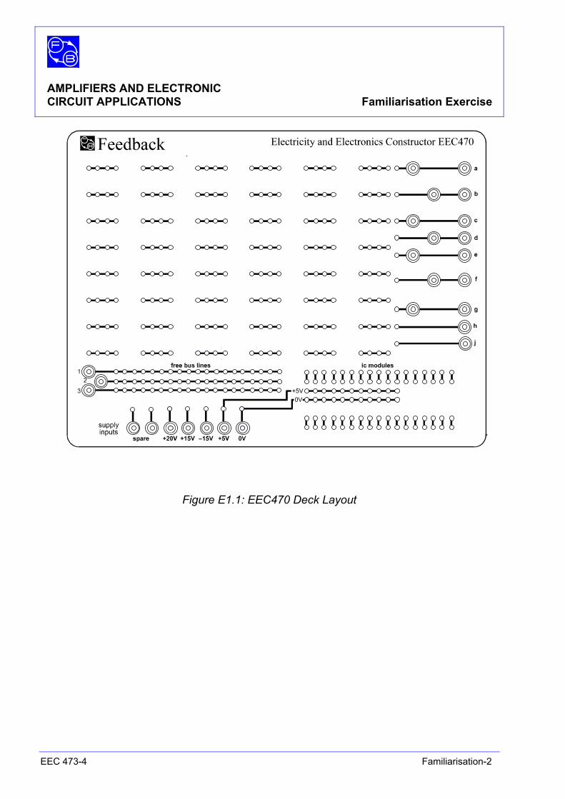
Figure E1.1: EEC470 Deck Layout
AMPLIFIERS AND ELECTRONIC CIRCUIT APPLICATIONS Familiarisation Exercise
EEC 473-4 Familiarisation-3
INTRODUCTION The Electricity & Electronics Constructor EEC470 is an unpowered mounting deck suitable for the construction of a wide variety of circuits which employ:
Discrete components Resistors, capacitors, transistors, etc.
Integrated circuits Analogue or digital.
Power components Thyristors and power transistors. The deck is used in conjunction with external power supplies
and with various kits of components covering different areas of industrial electronics. Each kit is self-contained and is provided with a book of student assignments, of which this familiarisation assignment is always the first.
THE DECK LAYOUT The layout of the EEC470 Deck is as shown in fig E1.1. The deck is supported by the following: Discrete Components These are supplied in the various kits on two, three and four-
pin carriers. Interlinking is done by 'shorting' links on two-pin carriers or by flexible 'patching' leads with 2 mm pin terminations.
Integrated Circuit Modules These are supplied, where appropriate, in the standard module
form used by Feedback in other digital and analogue constructional systems.
Many of these modules, particularly the digital types, obtain their power supply from the +5 V and 0 V bus-bars built in to this section. Other types will require power to be connected by patching leads.
Power Components There is provision for inserting up to two semi-conductors mounted on heat sinks. The section is also useful for coupling to external equipment, using 2 mm patch leads internally and 4mm leads externally.
Power Supplies External supplies can be brought in on 4 mm leads and patched internally using 2 mm leads. The supplies listed on the panel are those available from the Feedback 92-445 Power Supply unit or the optional Teknikit 92-100 console, both of which are designed for use with EEC470.
AMPLIFIERS AND ELECTRONIC CIRCUIT APPLICATIONS Familiarisation Exercise
EEC 473-4 Familiarisation-4
The current ratings of the 92-445 power supply or the 92-100 Teknikit Console are as follows, and any similar power supplies may be used as available:
— Variable. dc V 0 to 20 V regulated d.c. at 350 mA. — Fixed dc V + 5 V regulated dc at 1 A.
±15 V regulated d.c. at 300 mA. — ac supplies 12 V rms; 50 or 60 Hz supplied at
300 mA (isolated from other supplies). Connecting Leads
Q'ty Plug Length Colour Reference Dia . 9 4 mm 450 mm. 1 each of:– brown, red, orange,
yellow, green, blue, grey, white and black.
4 2/4 mm 450 mm 2 each of:– red and black. 3 2 mm 300 mm Red. 8 2 mm 150 mm Orange. 8 2 mm 150 mm Yellow. 5 2 mm 10 0mm Green.
PATCHING CONNECTIONS Connections which are shown ' - - - - - - - - - ' in the patching
diagrams for any given assignment indicate alterations to the basic circuit, and are correspondingly described in the text.

A
MPL
IFIE
RS
AN
D E
LEC
TRO
NIC
C
IRC
UIT
APP
LIC
ATI
ON
S Fa
mili
aris
atio
n Ex
erci
se
EE
C 4
73-4
Fa
mili
aris
atio
n-5
N
otes
AMPLIFIERS AND ELECTRONIC CIRCUIT APPLICATIONS Familiarisation Exercise
EEC 473-4 Familiarisation-6
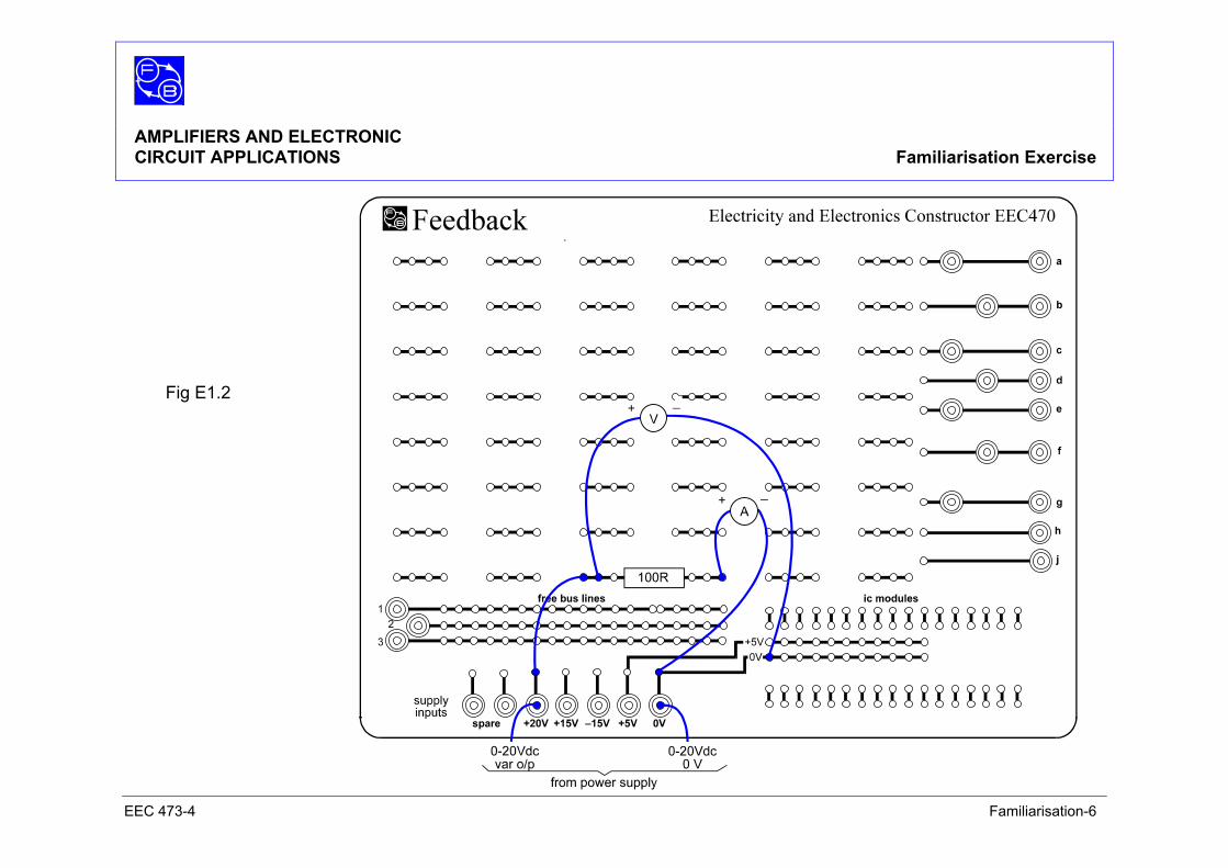
Fig E1.2
AMPLIFIERS AND ELECTRONIC CIRCUIT APPLICATIONS Familiarisation Exercise
EEC 473-4 Familiarisation-7
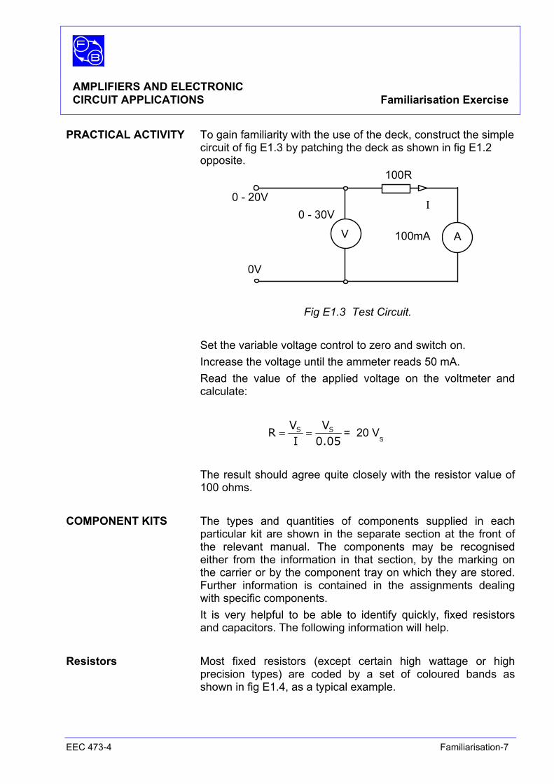
PRACTICAL ACTIVITY To gain familiarity with the use of the deck, construct the simple circuit of fig E1.3 by patching the deck as shown in fig E1.2 opposite.
V A
100R
I0 - 30V
0V
0 - 20V
100mA
Fig E1.3 Test Circuit. Set the variable voltage control to zero and switch on. Increase the voltage until the ammeter reads 50 mA. Read the value of the applied voltage on the voltmeter and
calculate:
0.05V
IV
R SS == = 20 VS
The result should agree quite closely with the resistor value of
100 ohms. COMPONENT KITS The types and quantities of components supplied in each
particular kit are shown in the separate section at the front of the relevant manual. The components may be recognised either from the information in that section, by the marking on the carrier or by the component tray on which they are stored. Further information is contained in the assignments dealing with specific components.
It is very helpful to be able to identify quickly, fixed resistors and capacitors. The following information will help.
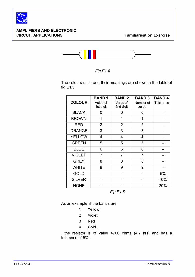
Resistors Most fixed resistors (except certain high wattage or high
precision types) are coded by a set of coloured bands as shown in fig E1.4, as a typical example.
AMPLIFIERS AND ELECTRONIC CIRCUIT APPLICATIONS Familiarisation Exercise
EEC 473-4 Familiarisation-8
Fig E1.4 The colours used and their meanings are shown in the table of
fig E1.5.
BAND 1 BAND 2 BAND 3 BAND 4 COLOUR Value of Value of Number of Tolerance 1st digit 2nd digit zeros
BLACK 0 0 0 – BROWN 1 1 1 – RED 2 2 2 – ORANGE 3 3 3 – YELLOW 4 4 4 – GREEN 5 5 5 – BLUE 6 6 6 – VIOLET 7 7 7 – GREY 8 8 8 – WHITE 9 9 9 – GOLD – – – 5% SILVER – – – 10% NONE – – – 20%
Fig E1.5 As an example, if the bands are: 1 Yellow 2 Violet 3 Red 4 Gold... ...the resistor is of value 4700 ohms (4.7 kΩ) and has a
tolerance of 5%.
AMPLIFIERS AND ELECTRONIC CIRCUIT APPLICATIONS Familiarisation Exercise
EEC 473-4 Familiarisation-9
Capacitors Capacitors are sometimes colour-coded but more usually they have the value printed on the body.
There is a good deal of variation between makers in the exact form of the markings but most use the normal units of picofarad (pF), nanofarad (nF) or the microfarad (µF). Often the F is omitted and sometimes, when there is no chance of confusion, the other letter also.
Example 0.47 µF could appear as 0.47 µ or just 0.47. This could
not be 0.47 pF, as it would be too low a value for any fixed capacitor. It could not be 0.47 nF either because such a value would be expressed as 470 pF.
The tolerance and voltage rating of a capacitor are also often
printed on the body, again. with or without units. Thus you could find:
1.0 µF ±20% 160V DC WKG or just ; 1.0/20/160 Large value capacitors (greater than about 1 µF) are usually
electrolytic types, which MUST be correctly polarised. Usually one of the terminals is marked with a + or a – and the capacitor must be inserted so as to apply the correct polarity.
AMPLIFIERS AND ELECTRONIC CIRCUIT APPLICATIONS Familiarisation Exercise
EEC 473-4 Familiarisation-10
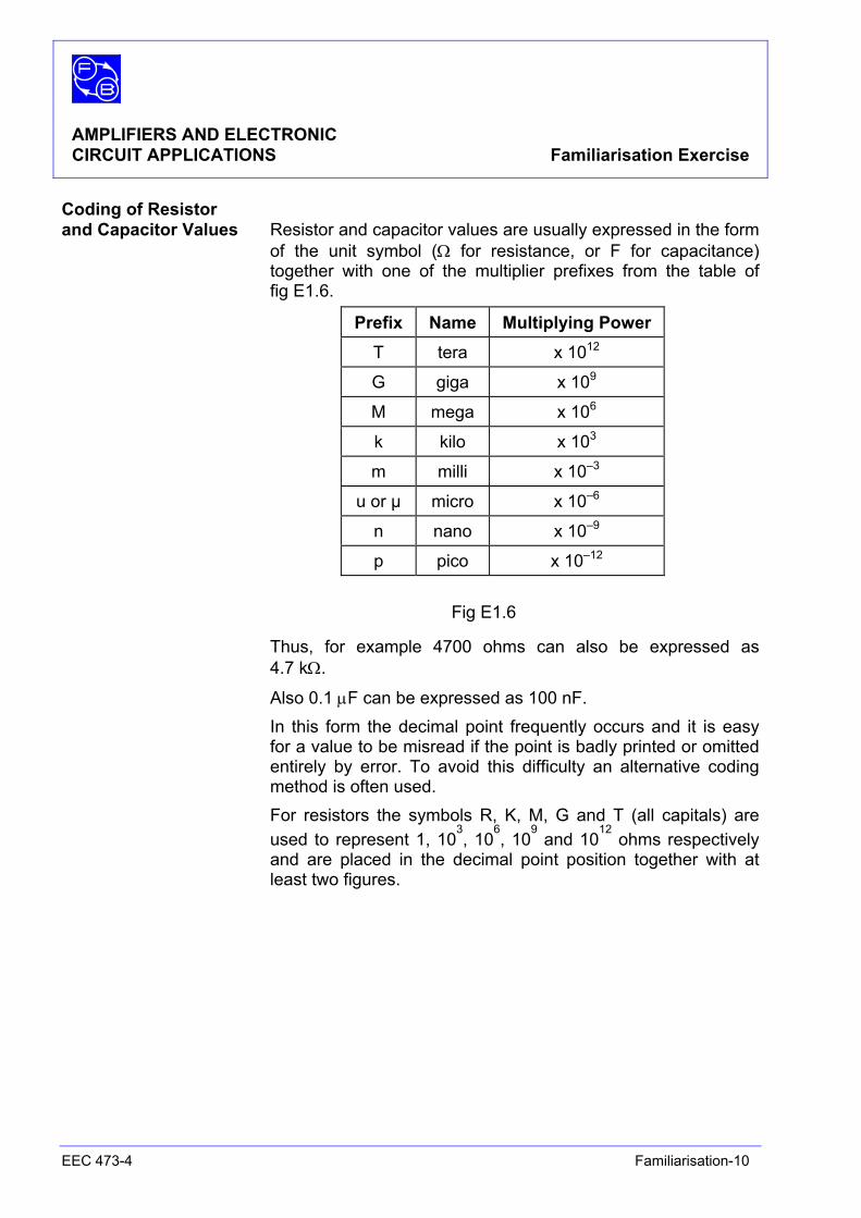
Coding of Resistor and Capacitor Values Resistor and capacitor values are usually expressed in the form
of the unit symbol (Ω for resistance, or F for capacitance) together with one of the multiplier prefixes from the table of fig E1.6.
Prefix Name Multiplying Power T tera x 1012
G giga x 109
M mega x 106
k kilo x 103
m milli x 10–3
u or µ micro x 10–6
n nano x 10–9
p pico x 10–12
Fig E1.6
Thus, for example 4700 ohms can also be expressed as 4.7 kΩ.
Also 0.1 µF can be expressed as 100 nF. In this form the decimal point frequently occurs and it is easy
for a value to be misread if the point is badly printed or omitted entirely by error. To avoid this difficulty an alternative coding method is often used.
For resistors the symbols R, K, M, G and T (all capitals) are used to represent 1, 10
3, 10
6, 10
9 and 10
12 ohms respectively
and are placed in the decimal point position together with at least two figures.
AMPLIFIERS AND ELECTRONIC CIRCUIT APPLICATIONS Familiarisation Exercise
EEC 473-4 Familiarisation-11
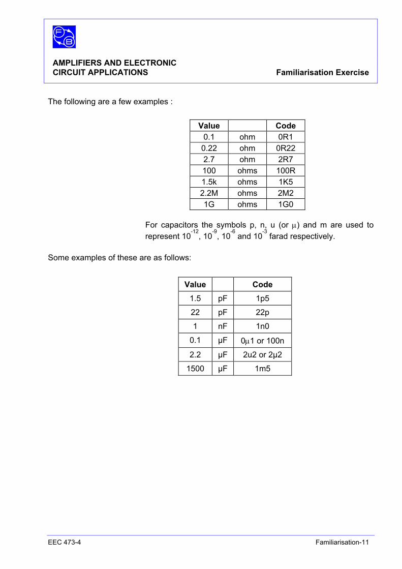
The following are a few examples :
Value Code 0.1 ohm 0R1 0.22 ohm 0R22 2.7 ohm 2R7 100 ohms 100R 1.5k ohms 1K5 2.2M ohms 2M2 1G ohms 1G0
For capacitors the symbols p, n, u (or µ) and m are used to
represent 10-12
, 10-9
, 10-6
and 10-3
farad respectively. Some examples of these are as follows:
Value Code 1.5 pF 1p5
22 pF 22p
1 nF 1n0
0.1 µF 0µ1 or 100n
2.2 µF 2u2 or 2µ2
1500 µF 1m5

AMPLIFIERS AND ELECTRONIC CIRCUIT APPLICATIONS Familiarisation Exercise
EEC 473-4 Familiarisation-12
Notes
Section 1 AMPLIFIERS AND ELECTRONIC CIRCUIT APPLICATIONS Amplifiers
EEC 473-4 1-1
Almost every electronic system uses an amplifier somewhere, and many systems use several different types. The two main types are: 1. Small signal amplifiers used, for example, to amplify the
small output signal from a transducer. 2. Power amplifiers used, for example, to operate a lamp or
loudspeaker. Power amplifiers are most important as they operate the
motors, valves and levers that make industrial automation possible.
The transistor is used extensively in both types of amplifier and enables highly complex systems to be quite small. Many of the small signal applications now employ integrated circuits whereby an entire amplifier (consisting of many separate components) can be made on one slice of silicon and be only a few millimetres across.
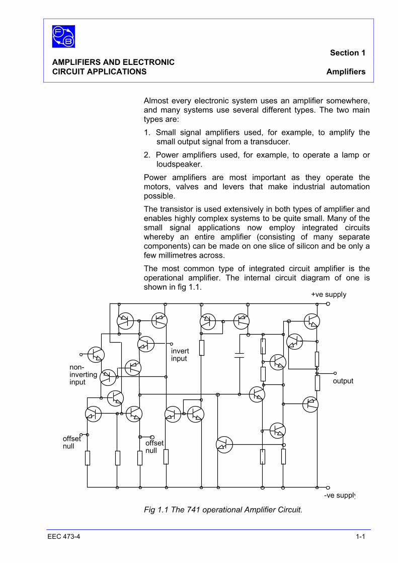
The most common type of integrated circuit amplifier is the operational amplifier. The internal circuit diagram of one is shown in fig 1.1.
non-invertinginput
offsetnull
offsetnull
+ve supply
output
-ve supply
invertinput
Fig 1.1 The 741 operational Amplifier Circuit.
Section 1 AMPLIFIERS AND ELECTRONIC CIRCUIT APPLICATIONS Amplifiers
EEC 473-4 1-2
The silicon slice is packaged in a small plastic pack. In
EEC471-2 the operation of the individual components was described. In the following section some of these components are used to make simple amplifiers and some examples of the applications of these amplifiers are given.
Assignment 1 AMPLIFIERS AND ELECTRONIC CIRCUIT APPLICATIONS Using Amplifiers
EEC 473-4 1-1-1
OBJECTIVE To investigate how, in an electronic amplifier, a
small d.c or a.c current can be made to control a much larger current.
EQUIPMENT REQUIRED Qty Apparatus 1 Electricity & Electronics Constructor
EEC470 1 Amplifier Kit EEC473-4 1 Power supply unit 0 to +20 V variable dc
regulated ±15 V dc regulated (eg, Feedback Power Supply 92-445, or optionally the 92-100 Teknikit console).
1 Function Generator 2 V pk to pk @ 40 Hz – 4 kHz. (eg, Feedback FG601 )
1 Multimeter or 1 Milliammeter 0 – 1 mA dc PREREQUISITE ASSIGNMENTS None KNOWLEDGE LEVEL Before working this assignment you should :
• Know the operation of the semi-conductor devices and circuits described in Feedback Manual EEC 471-2.
Assignment 1 AMPLIFIERS AND ELECTRONIC CIRCUIT APPLICATIONS Using Amplifiers
EEC 473-4 1-1-2
Notes
Assignment 1 AMPLIFIERS AND ELECTRONIC CIRCUIT APPLICATIONS Using Amplifiers
EEC 473-4 1-1-3
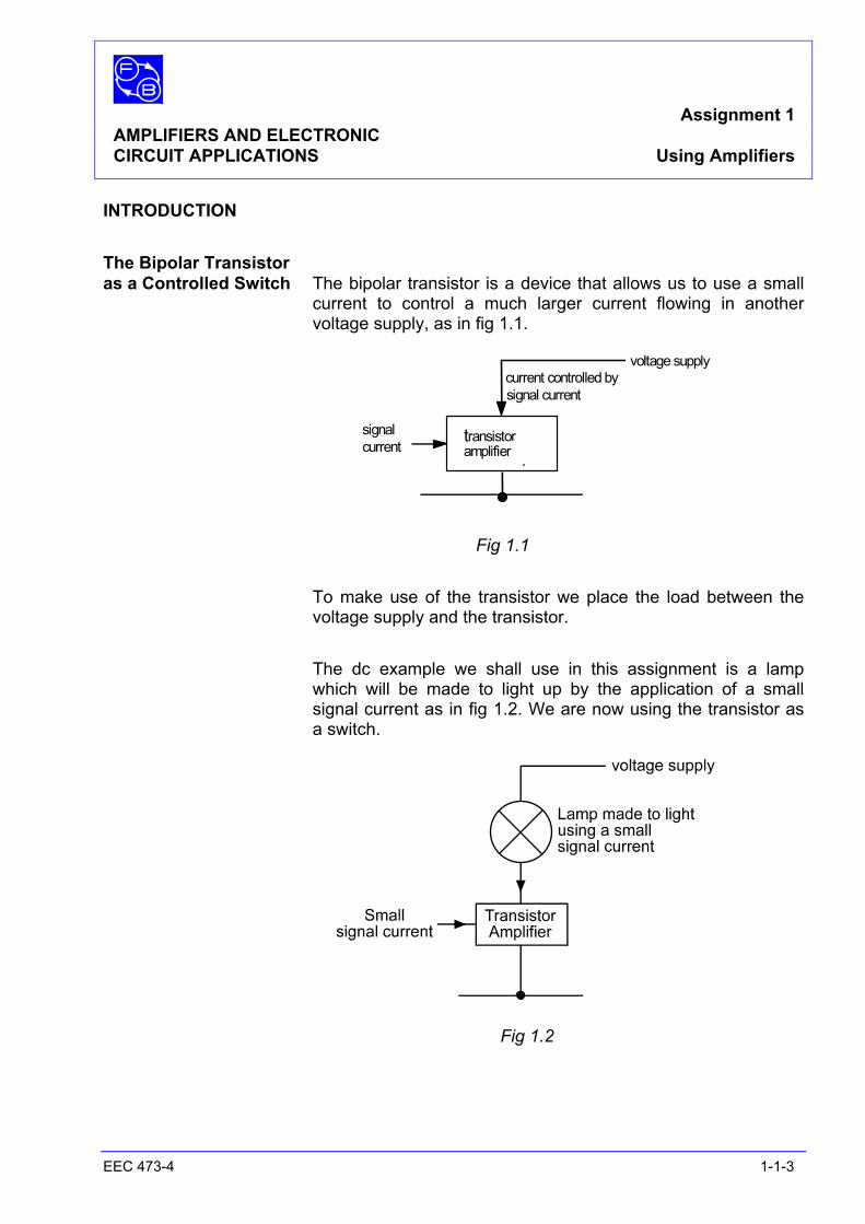
INTRODUCTION The Bipolar Transistor as a Controlled Switch The bipolar transistor is a device that allows us to use a small
current to control a much larger current flowing in another voltage supply, as in fig 1.1.
voltage supply
current controlled bysignal current
signalcurrent
transistor amplifier
Fig 1.1
To make use of the transistor we place the load between the voltage supply and the transistor.
The dc example we shall use in this assignment is a lamp
which will be made to light up by the application of a small signal current as in fig 1.2. We are now using the transistor as a switch.
Fig 1.2
Assignment 1 AMPLIFIERS AND ELECTRONIC CIRCUIT APPLICATIONS Using Amplifiers
EEC 473-4 1-1-4
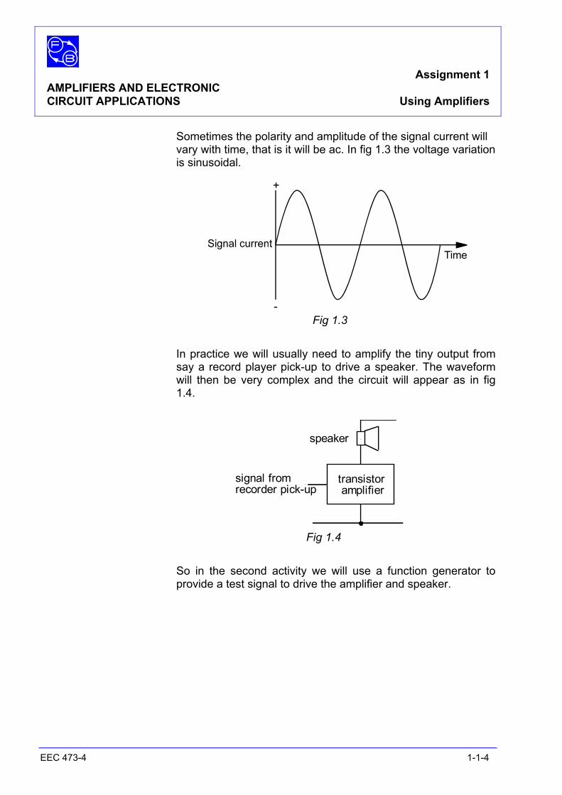
Sometimes the polarity and amplitude of the signal current will vary with time, that is it will be ac. In fig 1.3 the voltage variation is sinusoidal.
Fig 1.3 In practice we will usually need to amplify the tiny output from
say a record player pick-up to drive a speaker. The waveform will then be very complex and the circuit will appear as in fig 1.4.
speaker
transistor amplifier
signal fromrecorder pick-up
Fig 1.4
So in the second activity we will use a function generator to
provide a test signal to drive the amplifier and speaker.
Assignment 1 AMPLIFIERS AND ELECTRONIC CIRCUIT APPLICATIONS Using Amplifiers
EEC 473-4 1-1-5
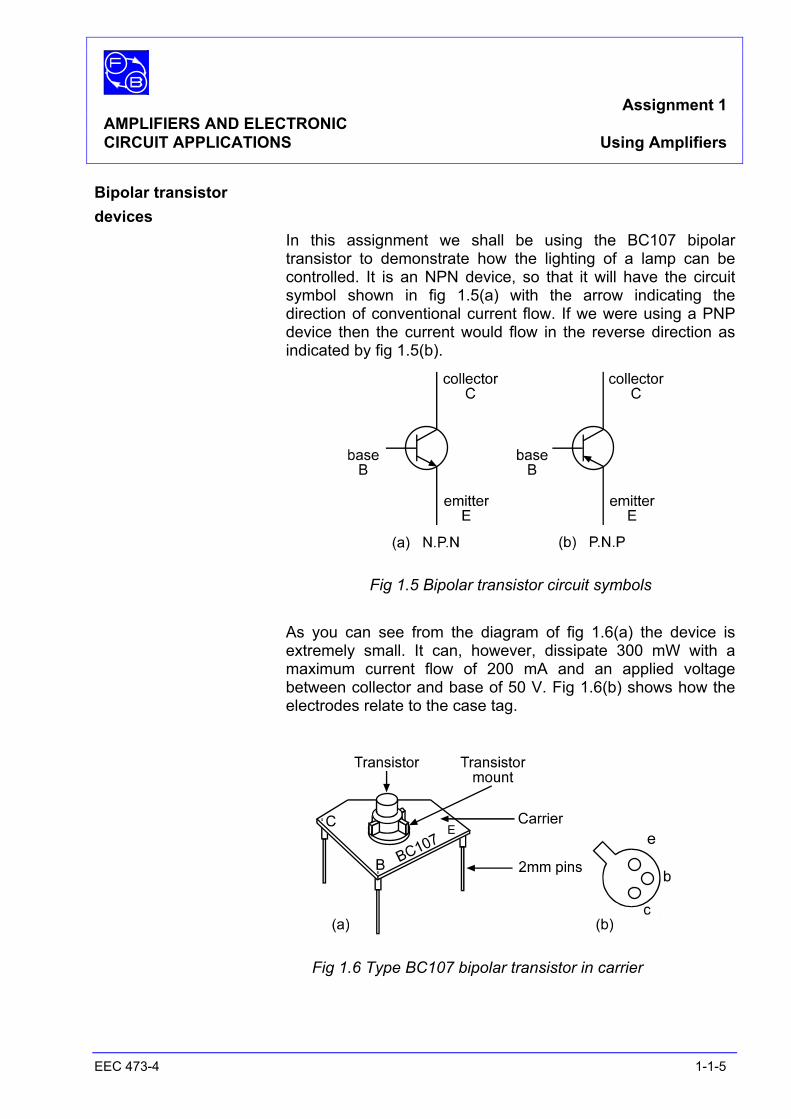
Bipolar transistor devices In this assignment we shall be using the BC107 bipolar
transistor to demonstrate how the lighting of a lamp can be controlled. It is an NPN device, so that it will have the circuit symbol shown in fig 1.5(a) with the arrow indicating the direction of conventional current flow. If we were using a PNP device then the current would flow in the reverse direction as indicated by fig 1.5(b).
Fig 1.5 Bipolar transistor circuit symbols
As you can see from the diagram of fig 1.6(a) the device is
extremely small. It can, however, dissipate 300 mW with a maximum current flow of 200 mA and an applied voltage between collector and base of 50 V. Fig 1.6(b) shows how the electrodes relate to the case tag.
Fig 1.6 Type BC107 bipolar transistor in carrier
E e

Assignment 1 AMPLIFIERS AND ELECTRONIC CIRCUIT APPLICATIONS Using Amplifiers
EEC 473-4 1-1-6
Notes

Ass
ignm
ent 1
A
MPL
IFIE
RS
AN
D E
LEC
TRO
NIC
CIR
CU
IT A
PPLI
CA
TIO
NS
Usi
ng A
mpl
ifier
s EE
C47
3-4
1-1-
7
Not
es
Assignment 1 AMPLIFIERS AND ELECTRONIC CIRCUIT APPLICATIONS Using Amplifiers
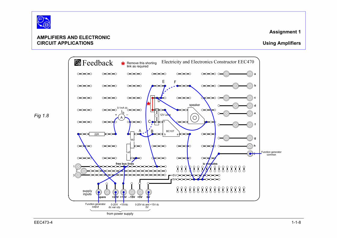
EEC473-4 1-1-8
Fig 1.8
Assignment 1 AMPLIFIERS AND ELECTRONIC CIRCUIT APPLICATIONS Using Amplifiers
EEC 473-4 1-1-9
EXPERIMENTAL PROCEDURE
In this part of the Assignment we shall show how an electronic amplifier can cause:
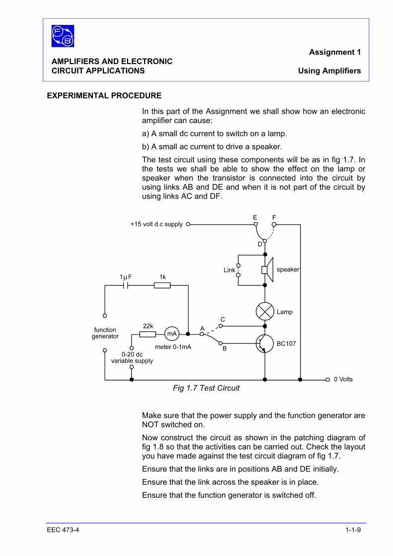
a) A small dc current to switch on a lamp. b) A small ac current to drive a speaker. The test circuit using these components will be as in fig 1.7. In
the tests we shall be able to show the effect on the lamp or speaker when the transistor is connected into the circuit by using links AB and DE and when it is not part of the circuit by using links AC and DF.
Fig 1.7 Test Circuit
Make sure that the power supply and the function generator are NOT switched on.
Now construct the circuit as shown in the patching diagram of fig 1.8 so that the activities can be carried out. Check the layout you have made against the test circuit diagram of fig 1.7.
Ensure that the links are in positions AB and DE initially. Ensure that the link across the speaker is in place. Ensure that the function generator is switched off.
Assignment 1 AMPLIFIERS AND ELECTRONIC CIRCUIT APPLICATIONS Using Amplifiers
EEC 473-4 1-1-10
DC Control of an Amplifier Turn on the power supply. Slowly turn up the variable voltage control until the lamp begins
to glow. A reading of about 200 µA on the meter should be sufficient.
The transistor amplifier is now in the circuit and a small current
flow into the base is making the transistor pass enough current to light up the lamp.
To show that the lamp does not light at all without the transistor
amplifier:
a. Turn off the power supply b. Move the link leads from AB and DE to AC
and DF on the layout c. Turn on the power supply and turn up the
variable voltage control until the meter again reads the small current.
The lamp does not light, showing that the small current alone is
insufficient to light the lamp. ac Control of an Amplifier Change the layout as follows, turn off the power supply and: a. Remove the link so that the speaker is now also in
circuit. b. Connect the link leads back to AB and DE so that
the transistor is now back in the circuit. c. Turn on the power supply, set the variable voltage
to zero and turn on the function generator. d. Set the frequency of the function generator to
400 Hz and increase the amplitude from zero until you hear a distinct buzzing noise coming from the speaker.
Note the output amplitude setting of the function generator.
Assignment 1 AMPLIFIERS AND ELECTRONIC CIRCUIT APPLICATIONS Using Amplifiers
EEC 473-4 1-1-11
To see if there is any sound from the speaker without the transistor in circuit:
e. Turn off the function generator. f. Reconnect the link leads across terminals AC and
DF. g. Turn on the function generator at the same output
amplitude setting. Note that any sound produced is much decreased in volume. You may wish to repeat this activity several times and vary the
frequency. Questions 1 What could you do if you found that the output
signal of a transistor amplifier stage was too small to give the current change required?
2 What do you think happens to the temperature
of the transistor when current flows through it? 3 What do you know about the effect on devices
that become too hot and what action do you think the designer takes to control this effect?
4 How would you go about testing a transistor to see if it was operating correctly?
Assignment 1 AMPLIFIERS AND ELECTRONIC CIRCUIT APPLICATIONS Using Amplifiers
EEC 473-4 1-1-12
PRACTICAL CONSIDERATIONS AND APPLICATIONS Transistor amplifiers are employed in almost every application
of electronic circuitry. Typical applications in the domestic field are in radio, television, and hi-fi equipment.
These are the general appliances that you know and can use but the amplifier also has a wide variety of industrial and commercial uses. Transmitting stations require them but in this application the components must be able to deal with a transmitted power that may be in kilowatts, and so will have completely different dimensions.
In industry, amplifiers are the mainstay for turning the small control signal output from computers into the powerful currents that can actually operate the electromechanical devices that now control the operation of machine tools.
In this kit you will learn the basic principles on which transistor amplifiers function and ways that malfunctions can be detected.
SUMMARY In this assignment you have learnt that: 1. A dc current too small to light a lamp will do so when
connected to the input of a transistor. 2. An ac current too small to operate a speaker will cause a
distinct sound when connected to the input of a transistor. 3. The signal source is separate from the power source
connected to the transistor outputs. 4. A small signal can be connected by line to an amplifier to
control a supply at a distance away.
Assignment 1 AMPLIFIERS AND ELECTRONIC CIRCUIT APPLICATIONS Answers
EEC 473-4 1-1-13
ANSWERS TO ASSIGNMENT 1 1 If one transistor stage is not enough to give the required
degree of amplification, then the designer can add one or more further stages to form a cascade amplifier.
This is shown in the transistor radio; a really minute signal received at the aerial can be used to drive the output speaker.
2 Current flowing in a transistor causes the dissipation of
electrical power in the form of heat. We have been told that the maximum power that the BC107
can dissipate without damage is 300 mW. A temperature rise occurs as a result of the power dissipation. In a hot climate or room the final temperature will be greater than in a cold environment.
3 There are limits to the temperature rise and too great a
temperature can seriously affect the correct operation of the system. The designer often uses a heat sink, to dissipate more effectively the heat generated and this is why the BC107 has a metal canister to give a good thermal contact to the heat sink.
4 We know that applying a signal to the base of the bipolar
transistor will cause a voltage change across the load. So all we have to do is see if this voltage change takes place. Very often an electronic unit has a maintenance manual in which the circuit is shown with the correct output voltages given. If the collector voltage is too high this will show poor amplification but if near earth then a short circuit may have occurred.
Assignment 1 AMPLIFIERS AND ELECTRONIC CIRCUIT APPLICATIONS Answers
EEC 473-4 1-1-14
Notes
Assignment 2 AMPLIFIERS AND ELECTRONIC CIRCUIT APPLICATIONS Gain
EEC 473-4 1-2-1
OBJECTIVES 1. Knowledge of the difference in behaviour between the bipolar and junction field effect transistors.
2. Knowledge of the dc gain of the bipolar and field effect transistors.
3. An understanding of ac voltage and current gain together with input impedance in the bipolar transistor.
4. An understanding of ac voltage gain in the field effect transistor.
EQUIPMENT REQUIRED Qty Apparatus 1 Electricity & Electronics Constructor
EEC470 1 Amplifier Kit EEC473-4 1 Power Supply Unit, 0 to 20 V variable dc
and ±15 V fixed dc regulated (eg, Feedback Power Supply 92-445 or optionally the 92-100 Teknikit console)
1 Function generator. Sinusoidal 8 V pk to pk @ 1 kHz ( eg, Feedback FG601 )
1 2–Channel Oscilloscope 2 Multimeters or 2 Voltmeters 5 V and 25 V dc and
2 Ammeters 50 µA and 10 mA dc PREREQUISITE ASSIGNMENTS Assignment 1
KNOWLEDGE LEVEL Before working this assignment you should :
• Know the operation of circuits handling combined ac and dc voltages and currents.
• Know the meaning of the term 'dc bias'
Assignment 2 AMPLIFIERS AND ELECTRONIC CIRCUIT APPLICATIONS Gain
EEC 473-4 1-2-2
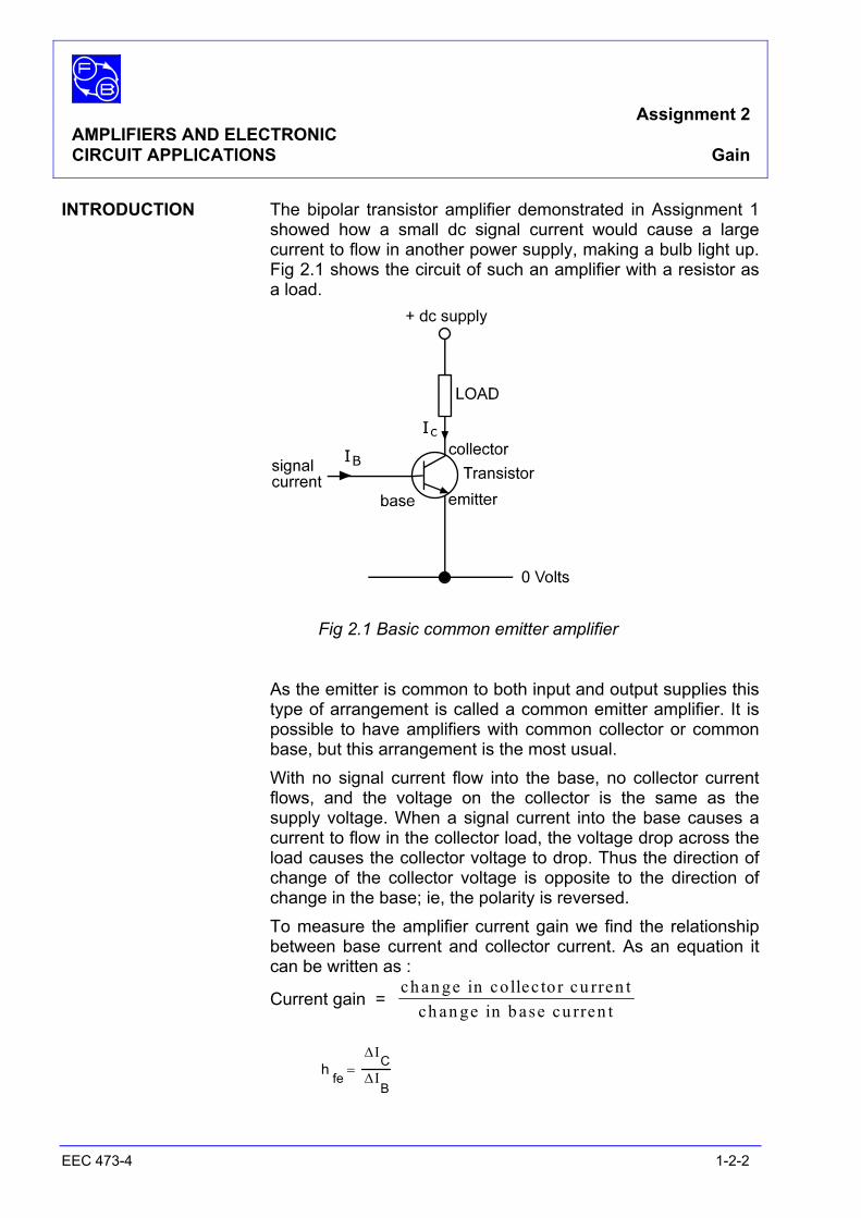
INTRODUCTION The bipolar transistor amplifier demonstrated in Assignment 1 showed how a small dc signal current would cause a large current to flow in another power supply, making a bulb light up. Fig 2.1 shows the circuit of such an amplifier with a resistor as a load.
Fig 2.1 Basic common emitter amplifier
As the emitter is common to both input and output supplies this type of arrangement is called a common emitter amplifier. It is possible to have amplifiers with common collector or common base, but this arrangement is the most usual.
With no signal current flow into the base, no collector current flows, and the voltage on the collector is the same as the supply voltage. When a signal current into the base causes a current to flow in the collector load, the voltage drop across the load causes the collector voltage to drop. Thus the direction of change of the collector voltage is opposite to the direction of change in the base; ie, the polarity is reversed.
To measure the amplifier current gain we find the relationship between base current and collector current. As an equation it can be written as :
Current gain = ch an ge in collec tor cu rren t
ch an ge in b ase cu rren t
h
fe=
∆IC
∆IB

Ass
ignm
ent 2
A
MPL
IFIE
RS
AN
D E
LEC
TRO
NIC
CIR
CU
IT A
PPLI
CA
TIO
NS
Gai
n EE
C 4
73-4
1-
2-3
Not
es
Assignment 2 AMPLIFIERS AND ELECTRONIC CIRCUIT APPLICATIONS Gain
EEC 473-4 1-2-4
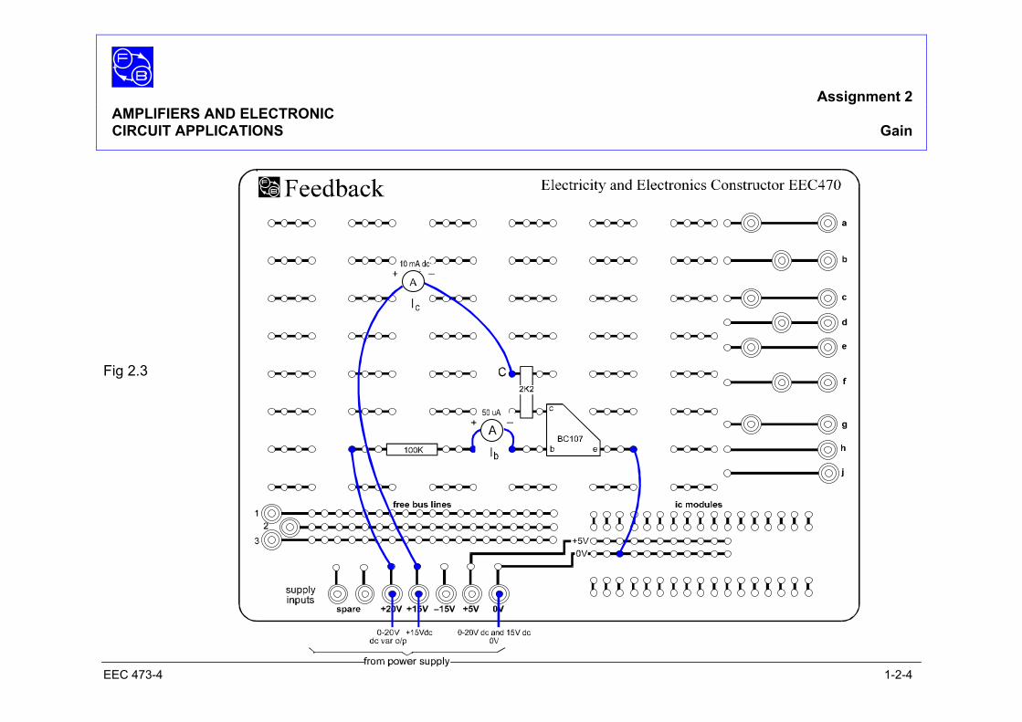
Fig 2.3
Assignment 2 AMPLIFIERS AND ELECTRONIC CIRCUIT APPLICATIONS Gain
EEC 473-4 1-2-5
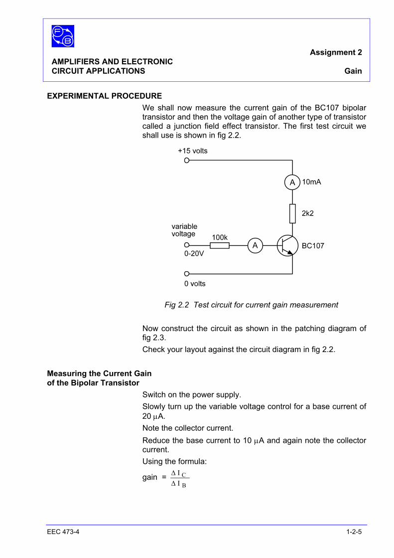
EXPERIMENTAL PROCEDURE We shall now measure the current gain of the BC107 bipolar
transistor and then the voltage gain of another type of transistor called a junction field effect transistor. The first test circuit we shall use is shown in fig 2.2.
Fig 2.2 Test circuit for current gain measurement Now construct the circuit as shown in the patching diagram of
fig 2.3. Check your layout against the circuit diagram in fig 2.2. Measuring the Current Gain of the Bipolar Transistor Switch on the power supply. Slowly turn up the variable voltage control for a base current of
20 µA. Note the collector current. Reduce the base current to 10 µA and again note the collector
current. Using the formula:
gain = ∆∆
II
C
B
Assignment 2 AMPLIFIERS AND ELECTRONIC CIRCUIT APPLICATIONS Gain
EEC 473-4 1-2-6
= ( ) ( )I I A I I A
A AC B C B= − =
−
2 0 1 02 0 1 0µ µ
µ µ
Calculate the dc current gain.
Questions 1 What is the dc current gain?
Turn up the variable voltage control until the collector current ceases to increase. Make a note of the value of the maximum collector current and the base current required.
2 Why does the collector current reach a maximum
value? Notice that the current gain in this bipolar transistor
amplifier is independent of the other component values in the circuit. It depends only on the physical properties of the transistor
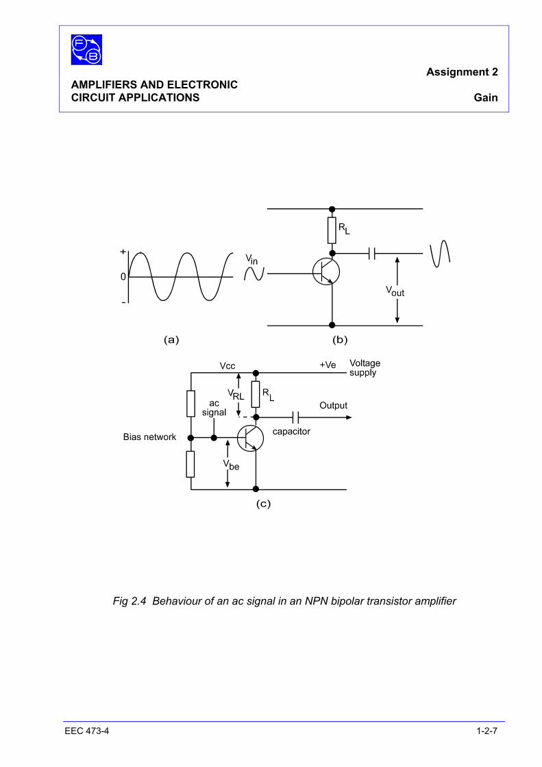
A.C. AMPLIFIERS We have seen how the bipolar transistor is able to amplify steady dc signals applied to the base. In this activity we will learn how a transistor amplifier can amplify ac signals. An ac signal is shown in fig 2.4(a). As you can see the signal changes polarity every half cycle so it is necessary to supply the transistor with a dc bias signal so that it amplifies over the entire cycle. A test circuit is shown in fig 2.4(b). The varying collector current will cause a voltage drop across the load resistor RL which will be opposite in polarity to the input signal. The output is taken from the capacitor. Fig 2.4(c) shows the voltages at important points in the circuit.
Note: Remember to change the collector current to µA before doing the calculation.
Assignment 2 AMPLIFIERS AND ELECTRONIC CIRCUIT APPLICATIONS Gain
EEC 473-4 1-2-7
Fig 2.4 Behaviour of an ac signal in an NPN bipolar transistor amplifier
Assignment 2 AMPLIFIERS AND ELECTRONIC CIRCUIT APPLICATIONS Gain
EEC 473-4 1-2-8
Amplifier Classification The type of amplifier we have just described amplifies the entire cycle of the ac input signal. It is called a Class A amplifier. In some applications we only require the positive half of the cycle to be amplified. A dc bias voltage is not required in this case. It is then called a Class B amplifier.
A.C Gain 1. Voltage Gain: This can be found by measuring the ratio of the peak-to-peak
collector-emitter and base-emitter signal voltages. Voltage Gain =
EmitterBaseEmitterCollector
−− peak–to–peak voltages
2. Current Gain: This can be found by measuring the ratio of the peak-to-peak
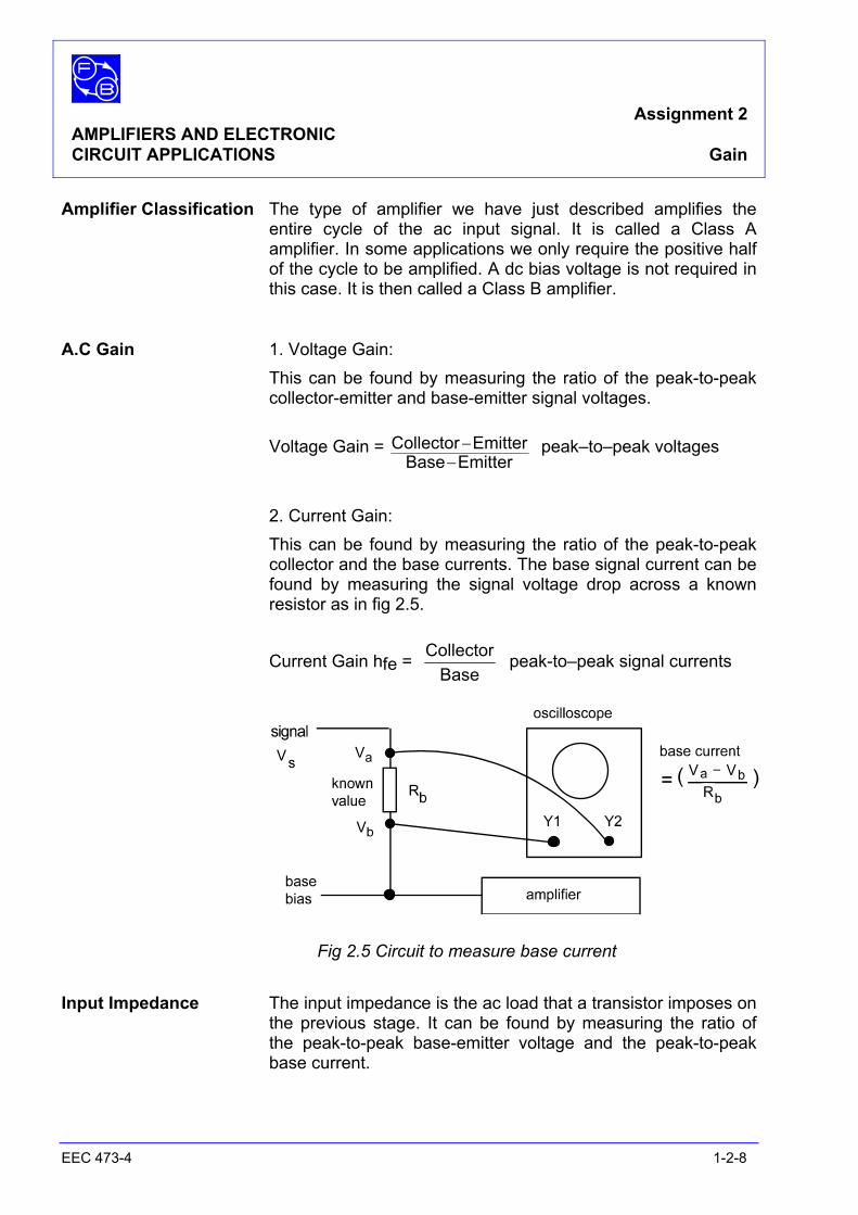
collector and the base currents. The base signal current can be found by measuring the signal voltage drop across a known resistor as in fig 2.5.
Current Gain hfe = Base
Collector peak-to–peak signal currents
Fig 2.5 Circuit to measure base current Input Impedance The input impedance is the ac load that a transistor imposes on
the previous stage. It can be found by measuring the ratio of the peak-to-peak base-emitter voltage and the peak-to-peak base current.
Assignment 2 AMPLIFIERS AND ELECTRONIC CIRCUIT APPLICATIONS Gain
EEC 473-4 1-2-9
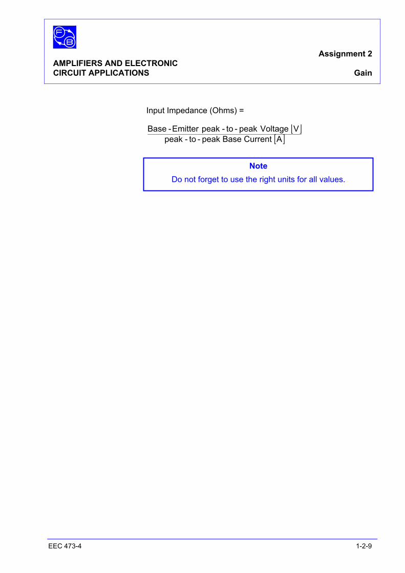
Input Impedance (Ohms) = [ ]
[ ]A Current Base peak -to-peakV Voltagepeak-to-peakEmitter-Base
Note Do not forget to use the right units for all values.

Assignment 2 AMPLIFIERS AND ELECTRONIC CIRCUIT APPLICATIONS Gain
EEC 473-4 1-2-10
Notes

Ass
ignm
ent 2
A
MPL
IFIE
RS
AN
D E
LEC
TRO
NIC
CIR
CU
IT A
PPLI
CA
TIO
NS
Gai
n EE
C 4
73-4
1-
2-11
Not
es
Assignment 2 AMPLIFIERS AND ELECTRONIC CIRCUIT APPLICATIONS Gain
EEC 473-4 1-2-12
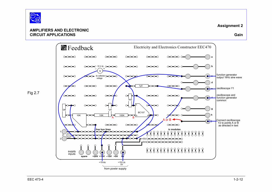
Fig 2.7
Assignment 2 AMPLIFIERS AND ELECTRONIC CIRCUIT APPLICATIONS Gain
EEC 473-4 1-2-13
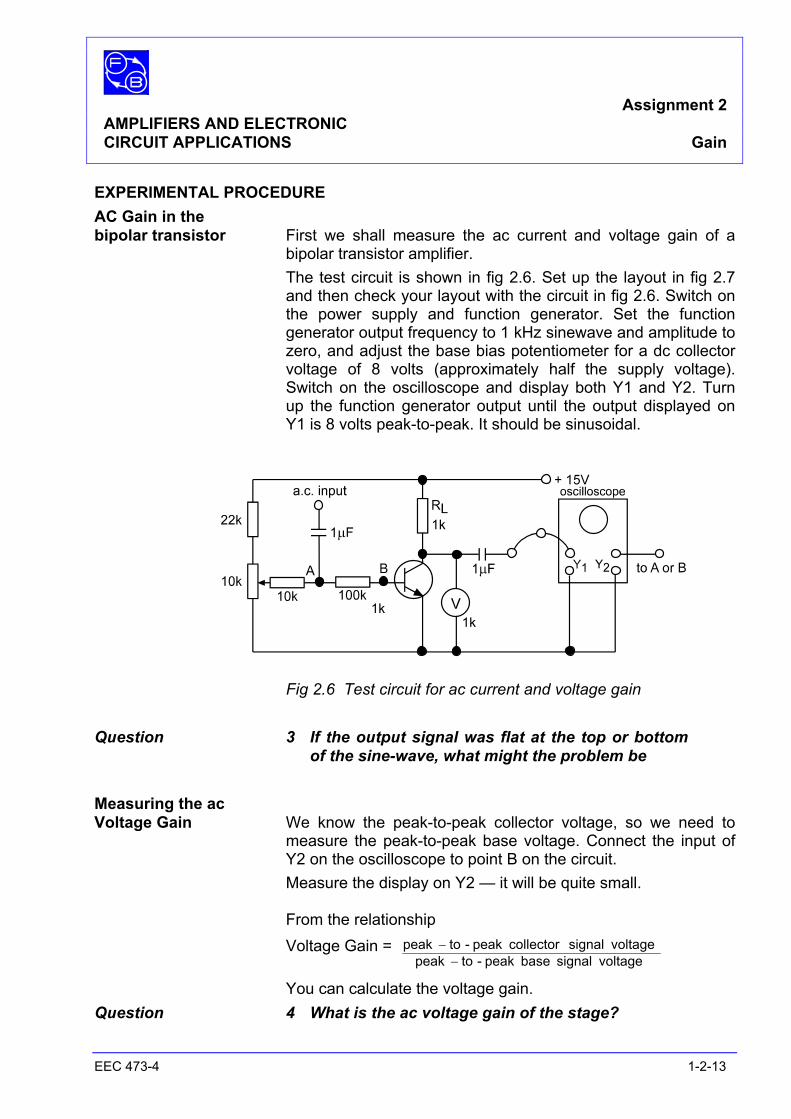
EXPERIMENTAL PROCEDURE AC Gain in the bipolar transistor First we shall measure the ac current and voltage gain of a
bipolar transistor amplifier. The test circuit is shown in fig 2.6. Set up the layout in fig 2.7
and then check your layout with the circuit in fig 2.6. Switch on the power supply and function generator. Set the function generator output frequency to 1 kHz sinewave and amplitude to zero, and adjust the base bias potentiometer for a dc collector voltage of 8 volts (approximately half the supply voltage). Switch on the oscilloscope and display both Y1 and Y2. Turn up the function generator output until the output displayed on Y1 is 8 volts peak-to-peak. It should be sinusoidal.
Fig 2.6 Test circuit for ac current and voltage gain Question 3 If the output signal was flat at the top or bottom
of the sine-wave, what might the problem be Measuring the ac Voltage Gain We know the peak-to-peak collector voltage, so we need to
measure the peak-to-peak base voltage. Connect the input of Y2 on the oscilloscope to point B on the circuit.
Measure the display on Y2 — it will be quite small. From the relationship Voltage Gain =
voltage signal base peak - topeakvoltage signal collectorpeak-topeak
−−
You can calculate the voltage gain. Question 4 What is the ac voltage gain of the stage?
Assignment 2 AMPLIFIERS AND ELECTRONIC CIRCUIT APPLICATIONS Gain
EEC 473-4 1-2-14
Measuring the ac Current Gain We know the peak-to-peak collector signal voltage and we
know the value of the collector load resistor (1 kΩ). From Ohms Law we can calculate the peak-to-peak collector current.
peak-to-peak collector signal current =
resistor load collector
voltage resistor collector peak- to-peak
Now we need to know the peak-to-peak signal base current. We can calculate this by measuring the signal voltage drop across the resistor in series with the base (resistor A-B).
Measure the peak-to-peak signal voltage at point A. By subtracting the signal voltage at point B that we already know, we have the voltage across the resistor. In the same way as with the collector current we can obtain the base current. From the relationship:
peak-to-peak base current =
value resistor base
voltage resistor base peak -to-peak
We can now calculate the ac current gain: current gain =
current signal base peak-to-peak
currentsignalcollectorpeak-to-peak
Questions 5 What is the ac current gain? 6 Are the values of ac current and voltage gain
dependent on resistor values? Measurement of the Input Impedance We have the measurements required to calculate the input
impedance of the bipolar transistor operating as an amplifier. From the relationship:
Input impedance (Ohms) =
current base peak- to-peak Signalvoltage base peak- to-peak Signal
We can calculate the ac input impedance. Question 7 What is the ac input impedance?
Assignment 2 AMPLIFIERS AND ELECTRONIC CIRCUIT APPLICATIONS Gain
EEC 473-4 1-2-15
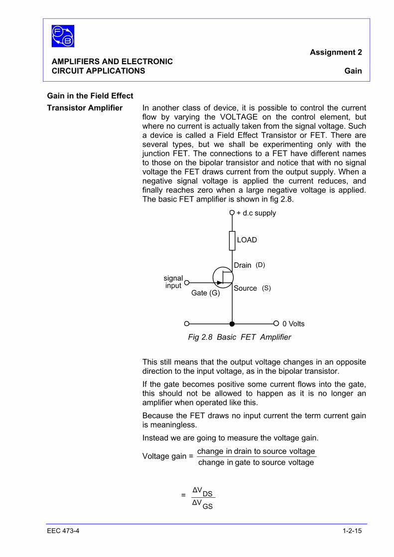
Gain in the Field Effect Transistor Amplifier In another class of device, it is possible to control the current
flow by varying the VOLTAGE on the control element, but where no current is actually taken from the signal voltage. Such a device is called a Field Effect Transistor or FET. There are several types, but we shall be experimenting only with the junction FET. The connections to a FET have different names to those on the bipolar transistor and notice that with no signal voltage the FET draws current from the output supply. When a negative signal voltage is applied the current reduces, and finally reaches zero when a large negative voltage is applied. The basic FET amplifier is shown in fig 2.8.
Fig 2.8 Basic FET Amplifier This still means that the output voltage changes in an opposite
direction to the input voltage, as in the bipolar transistor. If the gate becomes positive some current flows into the gate,
this should not be allowed to happen as it is no longer an amplifier when operated like this.
Because the FET draws no input current the term current gain is meaningless.
Instead we are going to measure the voltage gain.
Voltage gain = voltage source to gate in changevoltage source to drain in change
= GS∆VDS∆V
(D)
(S)
Assignment 2 AMPLIFIERS AND ELECTRONIC CIRCUIT APPLICATIONS Gain
EEC 473-4 1-2-16
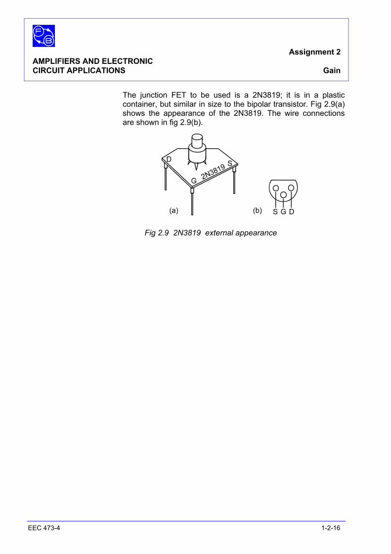
The junction FET to be used is a 2N3819; it is in a plastic container, but similar in size to the bipolar transistor. Fig 2.9(a) shows the appearance of the 2N3819. The wire connections are shown in fig 2.9(b).
Fig 2.9 2N3819 external appearance

Ass
ignm
ent 2
A
MPL
IFIE
RS
AN
D E
LEC
TRO
NIC
CIR
CU
IT A
PPLI
CA
TIO
NS
Gai
n EE
C 4
73-4
1-
2-17
Not
es
Assignment 2 AMPLIFIERS AND ELECTRONIC CIRCUIT APPLICATIONS Gain
EEC 473-4 1-2-18
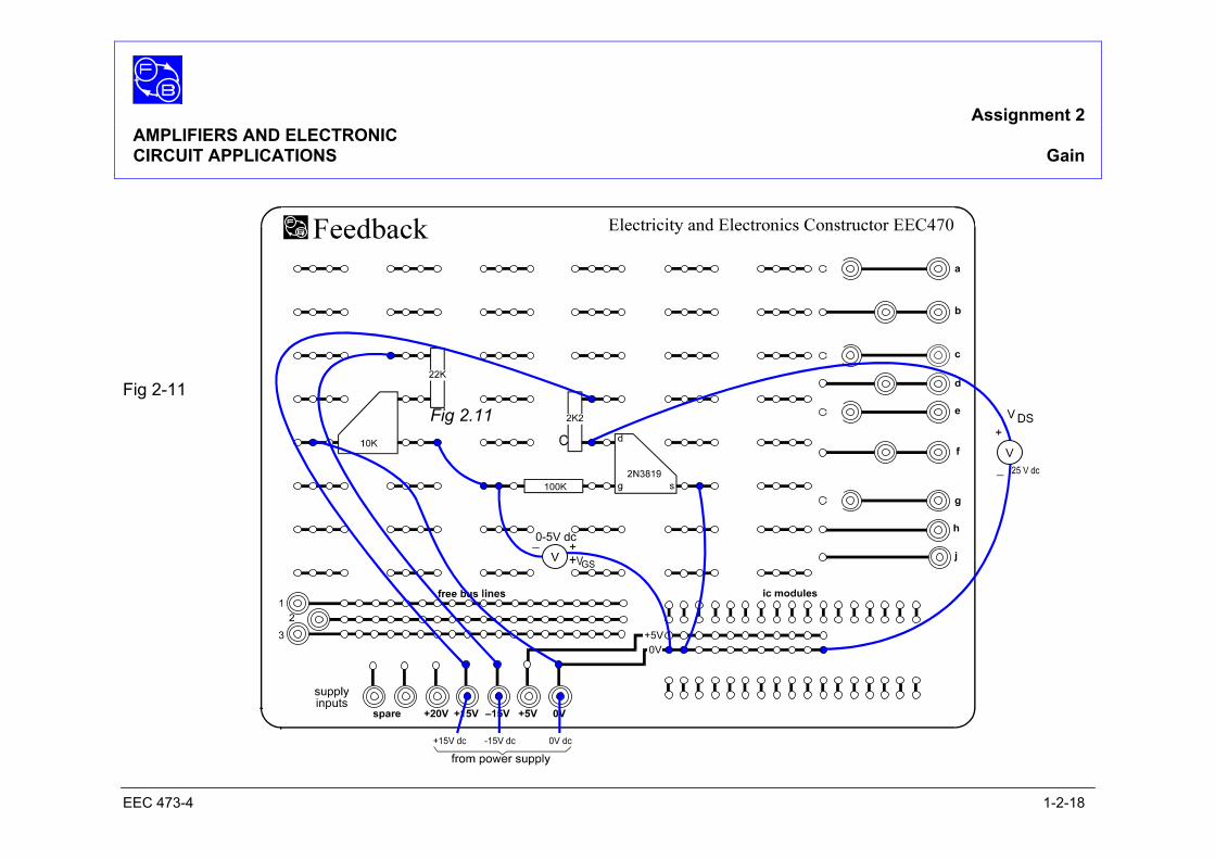
Fig 2-11 Fig 2.11
Assignment 2 AMPLIFIERS AND ELECTRONIC CIRCUIT APPLICATIONS Gain
EEC 473-4 1-2-19
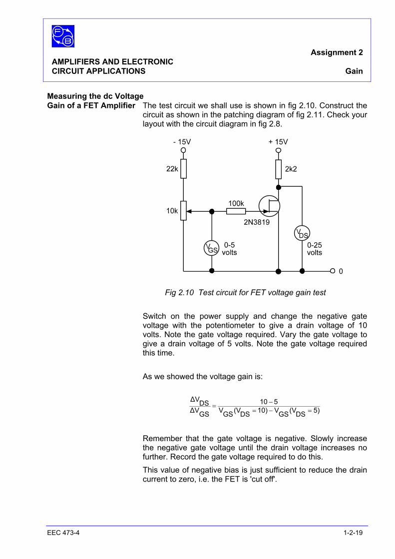
Measuring the dc Voltage Gain of a FET Amplifier The test circuit we shall use is shown in fig 2.10. Construct the
circuit as shown in the patching diagram of fig 2.11. Check your layout with the circuit diagram in fig 2.8.
Fig 2.10 Test circuit for FET voltage gain test Switch on the power supply and change the negative gate
voltage with the potentiometer to give a drain voltage of 10 volts. Note the gate voltage required. Vary the gate voltage to give a drain voltage of 5 volts. Note the gate voltage required this time.
As we showed the voltage gain is:
5)DS(VGSV10)DS(VGSV
510
GS∆VDS∆V
=−=−=
Remember that the gate voltage is negative. Slowly increase the negative gate voltage until the drain voltage increases no further. Record the gate voltage required to do this.
This value of negative bias is just sufficient to reduce the drain current to zero, i.e. the FET is 'cut off'.
Assignment 2 AMPLIFIERS AND ELECTRONIC CIRCUIT APPLICATIONS Gain
EEC 473-4 1-2-20
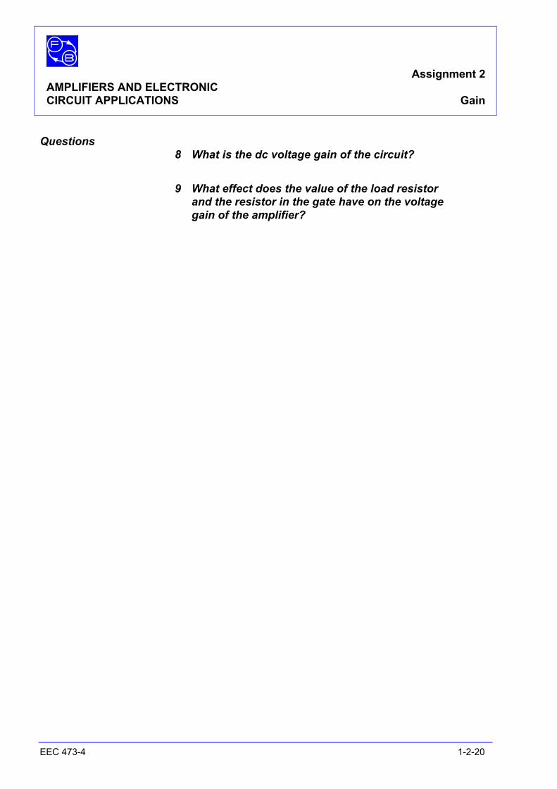
Questions 8 What is the dc voltage gain of the circuit? 9 What effect does the value of the load resistor
and the resistor in the gate have on the voltage gain of the amplifier?

Ass
ignm
ent 2
A
MPL
IFIE
RS
AN
D E
LEC
TRO
NIC
CIR
CU
IT A
PPLI
CA
TIO
NS
Gai
n EE
C 4
73-4
1-
2-21
Not
es
Assignment 2 AMPLIFIERS AND ELECTRONIC CIRCUIT APPLICATIONS Gain
EEC 473-4 1-2-22
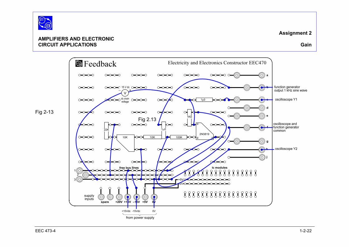
Fig 2-13 Fig 2.13
Assignment 2 AMPLIFIERS AND ELECTRONIC CIRCUIT APPLICATIONS Gain
EEC 473-4 1-2-23
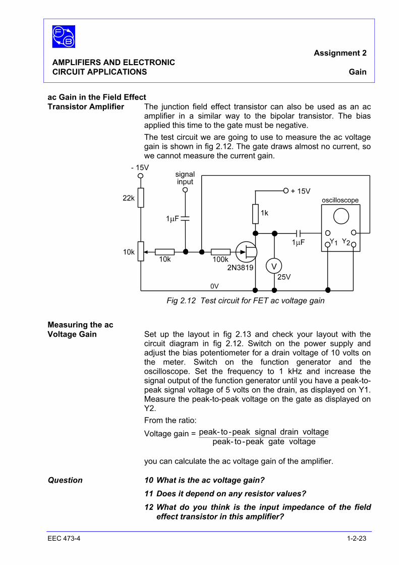
ac Gain in the Field Effect Transistor Amplifier The junction field effect transistor can also be used as an ac
amplifier in a similar way to the bipolar transistor. The bias applied this time to the gate must be negative.
The test circuit we are going to use to measure the ac voltage gain is shown in fig 2.12. The gate draws almost no current, so we cannot measure the current gain.
Fig 2.12 Test circuit for FET ac voltage gain Measuring the ac Voltage Gain Set up the layout in fig 2.13 and check your layout with the
circuit diagram in fig 2.12. Switch on the power supply and adjust the bias potentiometer for a drain voltage of 10 volts on the meter. Switch on the function generator and the oscilloscope. Set the frequency to 1 kHz and increase the signal output of the function generator until you have a peak-to-peak signal voltage of 5 volts on the drain, as displayed on Y1. Measure the peak-to-peak voltage on the gate as displayed on Y2.
From the ratio: Voltage gain =
voltage gate peak- to-peakvoltage drain signal peak-to-peak
you can calculate the ac voltage gain of the amplifier. Question 10 What is the ac voltage gain? 11 Does it depend on any resistor values? 12 What do you think is the input impedance of the field
effect transistor in this amplifier?
Assignment 2 AMPLIFIERS AND ELECTRONIC CIRCUIT APPLICATIONS Gain
EEC 473-4 1-2-24
PRACTICAL CONSIDERATIONS AND APPLICATIONS The application of amplifiers to ac amplification is very useful.
Many of the devices that we use every day make use of them. The telephone system, radio, television and industrial controls are examples.
Both the bipolar and field effect transistor are used in different applications, determined by the requirements for input impedance, voltage and current gain.
Testing for Malfunctions By using an oscilloscope the signal voltages on the input can
be examined and with a test meter the dc levels can be checked. If the fault is in the amplifier there will be a signal at the input but not at the output. If the bias is correct, but there is the wrong dc output level there is probably a transistor malfunction.
Using a function generator, like the FG601, a test signal can be injected into the amplifier for further tests. Input and output levels for both dc and signal are usually given in the service manual.
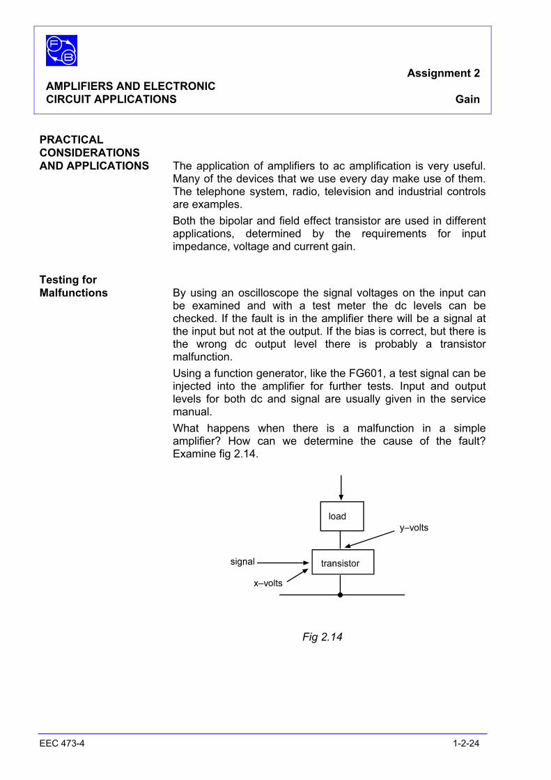
What happens when there is a malfunction in a simple amplifier? How can we determine the cause of the fault? Examine fig 2.14.
Fig 2.14
Assignment 2 AMPLIFIERS AND ELECTRONIC CIRCUIT APPLICATIONS Gain
EEC 473-4 1-2-25
Some tests we might do are: 1. Is there a signal input at x? If not the fault is probably not in
the amplifier. 2. If x is present, what is the value of y volts? If y volts are near zero the transistor may be short circuit. If y volts are different from the expected value the problem
may be in the load.
SUMMARY In this assignment you have learnt that: 1. The bipolar transistor is controlled by a flow of current into
the base. 2. The FET is controlled by the voltage on the gate. 3. The base supply voltage of the bipolar transistor is the same
polarity as the collector supply voltage. 4. The gate supply voltage of the FET is of opposite polarity to
the drain supply voltage. 5. The gate in a FET takes almost no current. 6. In order to amplify all the signal, dc bias is required. 7. The bipolar transistor input impedance is low, so it operates
on current. It has high current and voltage gain. 8. The FET input impedance is high, so it operates on voltage.
The voltage gain is low but the current gain is very high.
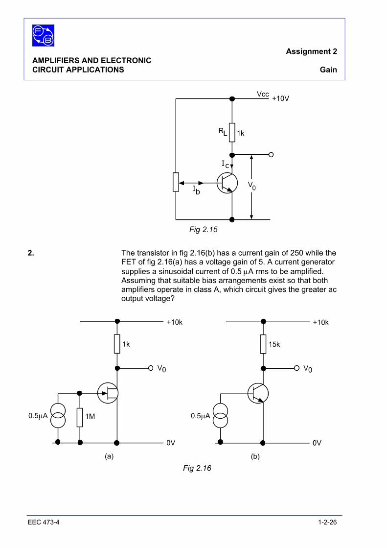
EXERCISES 1. The transistor in fig 2.15 has a current gain of 250. V0 is 5 volts. By how much must Ib change to cause V0 to become 7.5 volts?
Would Ib be greater or smaller than the initial value?
Assignment 2 AMPLIFIERS AND ELECTRONIC CIRCUIT APPLICATIONS Gain
EEC 473-4 1-2-26
Fig 2.15 2. The transistor in fig 2.16(b) has a current gain of 250 while the
FET of fig 2.16(a) has a voltage gain of 5. A current generator supplies a sinusoidal current of 0.5 µA rms to be amplified. Assuming that suitable bias arrangements exist so that both amplifiers operate in class A, which circuit gives the greater ac output voltage?
Fig 2.16
Assignment 2 AMPLIFIERS AND ELECTRONIC CIRCUIT APPLICATIONS Answers
EEC 473-4 1-2-27
ANSWERS TO ASSIGNMENT 2 1 It should be between 100-300. 2 Maximum current is determined by the load resistor
and the supply voltage. It cannot be greater than the Ohms Law value:
LoadCollector
Voltage SupplymaxI =
3 It probably means that the dc bias is wrongly set so that some of the signal is not amplified.
4 Typically it might be about 150. 5 Typically it might be about 200. 6 The ac current gain is independent of resistor values, but
the voltage gain depends on the collector load resistor.
7 It should be between1 to 3 kΩ 8 It should be about 10. 9 The value of the collector load determines the gain
of a stage as the gate voltage actually controls the drain current which produces a voltage change proportional to the load resistor. As the gate takes no current there can be no voltage drop across the resistor in series with the gate; so its value has little effect.
10 It should be about 4. 11 Yes, it depends on the load resistance like the other
voltage gains. 12 As we said the current taken by the gate is almost
zero so the input impedance must be very high. Certainly more than 1 MΩ. This can be very useful.
Assignment 2 AMPLIFIERS AND ELECTRONIC CIRCUIT APPLICATIONS Answers
EEC 473-4 1-2-28
Exercises 1. IC = LR
OVCCV −
If VO = 5 V : IC =
310510 − = 5 mA
When VO = 7.5 V : IC =
3107.510 − = 2.5 mA
Then ∆IC = 5 – 2.5 = 2.5 mA
B∆IC∆I
= 250
then 10 µ0250
32.5x10250
C∆IB∆I =
−==
The new current will be less than the initial value. Exercise 2a FET circuit
No current flows in the gate so all the current develops a voltage across the 1 MΩ resistor
Input voltage = 0.5 x 10
–6 x 10 6
= 0.5 V rms Output voltage = 0.5 x 5 = 2.5 V rms Exercise 2b Bipolar transistor circuit Output current = 0.5 x 10
–6 x 250 = 125 x 10
–6 A rms Output voltage = 125 x 10
–6 x 15 x 103
= 1.875 V rms So circuit 'a' gives greater output voltage
Assignment 3 AMPLIFIERS AND ELECTRONIC CIRCUIT APPLICATIONS Distortion
EEC 473-4 1-3-1
OBJECTIVES 1 To investigate why an output waveform limits, due to a negative or incorrect bias.
2. To investigate how the gain varies with input signal level.
3. To understand the cause and effect of frequency and phase distortion in a transistor amplifier as well as appreciate the interaction that occurs between wires at higher frequencies.
EQUIPMENT REQUIRED Qty Apparatus 1 Electricity & Electronics Constructor
EEC470 1 Amplifier Kit EEC473-4 1 Power supply unit +15 V dc regulated
(eg, Feedback Power Supply 92-445 or optionally the 92-100 Teknikit console)
1 Function generator Sinusoidal and Triangular 10 V pk-to-pk @ 1 kHz (eg, Feedback - FG601)
1 2–Channel Oscilloscope 1 Multimeter or 1 Voltmeter 50 V dc PREREQUISITE ASSIGNMENTS Assignment 2 KNOWLEDGE LEVEL Before working this assignment you should :
• Know how to sum ac quantities of differing amplitude and frequency.
Assignment 3 AMPLIFIERS AND ELECTRONIC CIRCUIT APPLICATIONS Distortion
EEC 473-4 1-3-2
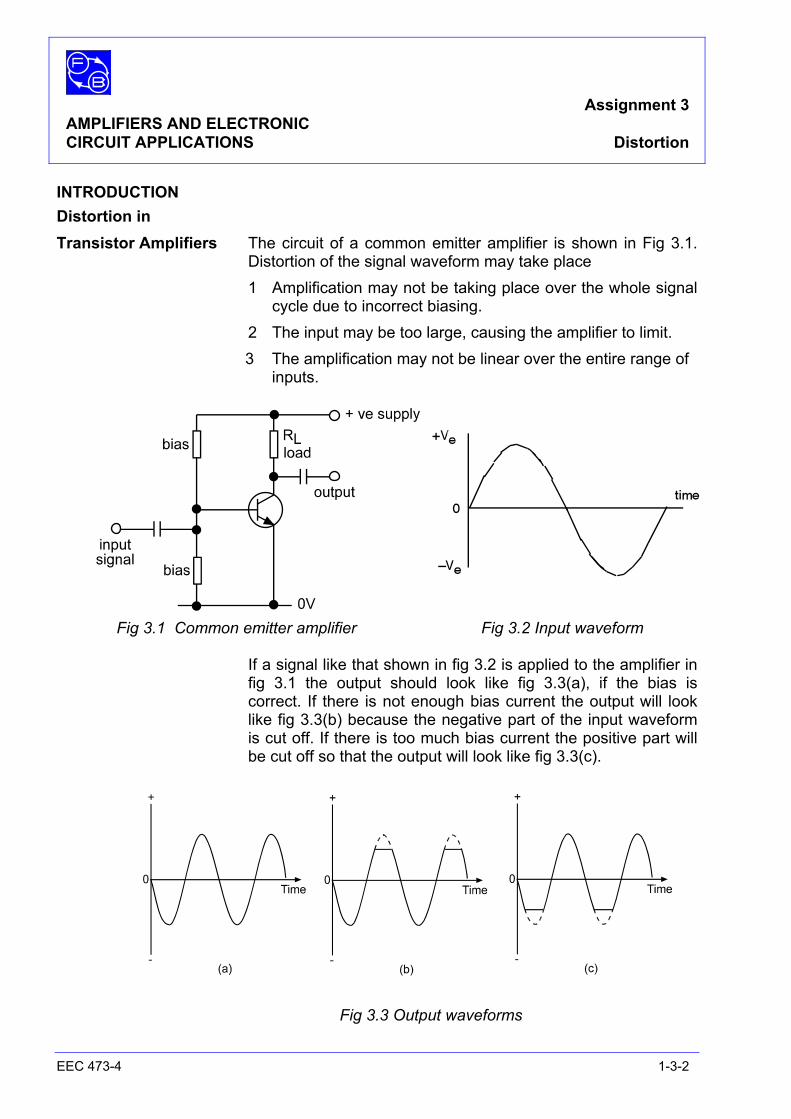
INTRODUCTION Distortion in Transistor Amplifiers The circuit of a common emitter amplifier is shown in Fig 3.1.
Distortion of the signal waveform may take place 1 Amplification may not be taking place over the whole signal
cycle due to incorrect biasing. 2 The input may be too large, causing the amplifier to limit.
3 The amplification may not be linear over the entire range of inputs.
Fig 3.1 Common emitter amplifier Fig 3.2 Input waveform If a signal like that shown in fig 3.2 is applied to the amplifier in
fig 3.1 the output should look like fig 3.3(a), if the bias is correct. If there is not enough bias current the output will look like fig 3.3(b) because the negative part of the input waveform is cut off. If there is too much bias current the positive part will be cut off so that the output will look like fig 3.3(c).
Fig 3.3 Output waveforms
Assignment 3 AMPLIFIERS AND ELECTRONIC CIRCUIT APPLICATIONS Distortion
EEC 473-4 1-3-3
Notice that the polarity of the output is opposite to that of the input waveform. When the bias current is too small, during the negative part of the cycle the transistor does not conduct and so the output is set by the supply voltage.
When the bias current is too great the positive part of the cycle saturates the transistor and the output drops almost to zero.
Limiting of both positive and negative parts of the cycle can occur when the input signal is too large, even when the bias current is correct.
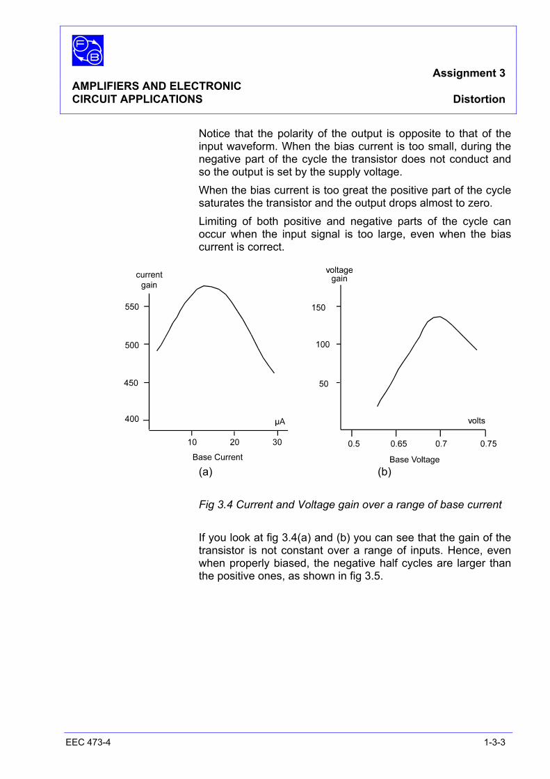
(a) (b) Fig 3.4 Current and Voltage gain over a range of base current If you look at fig 3.4(a) and (b) you can see that the gain of the
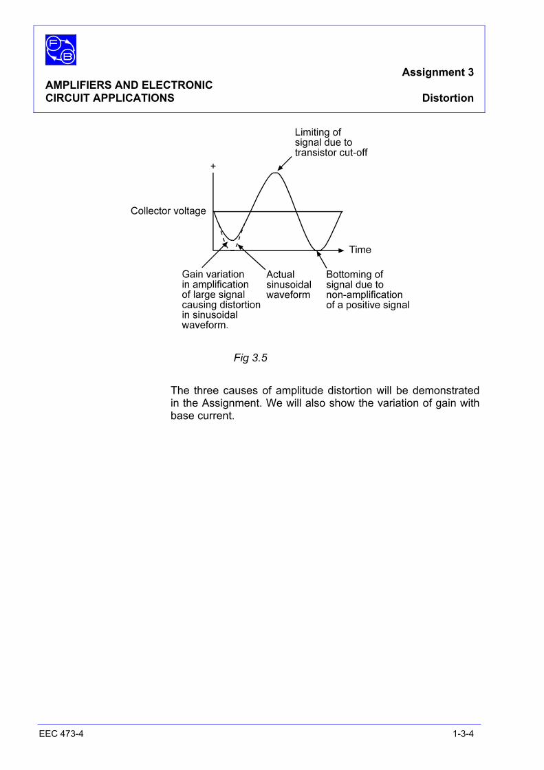
transistor is not constant over a range of inputs. Hence, even when properly biased, the negative half cycles are larger than the positive ones, as shown in fig 3.5.
Assignment 3 AMPLIFIERS AND ELECTRONIC CIRCUIT APPLICATIONS Distortion
EEC 473-4 1-3-4
Fig 3.5 The three causes of amplitude distortion will be demonstrated
in the Assignment. We will also show the variation of gain with base current.

Ass
ignm
ent 3
A
MPL
IFIE
RS
AN
D E
LEC
TRO
NIC
CIR
CU
IT A
PPLI
CA
TIO
NS
Dis
tort
ion
EE
C 4
73-4
1-
3-5
Not
es
Assignment 3 AMPLIFIERS AND ELECTRONIC CIRCUIT APPLICATIONS Distortion
EEC 473-4 1-3-6
Fig 3-7
Assignment 3 AMPLIFIERS AND ELECTRONIC CIRCUIT APPLICATIONS Distortion
EEC 473-4 1-3-7
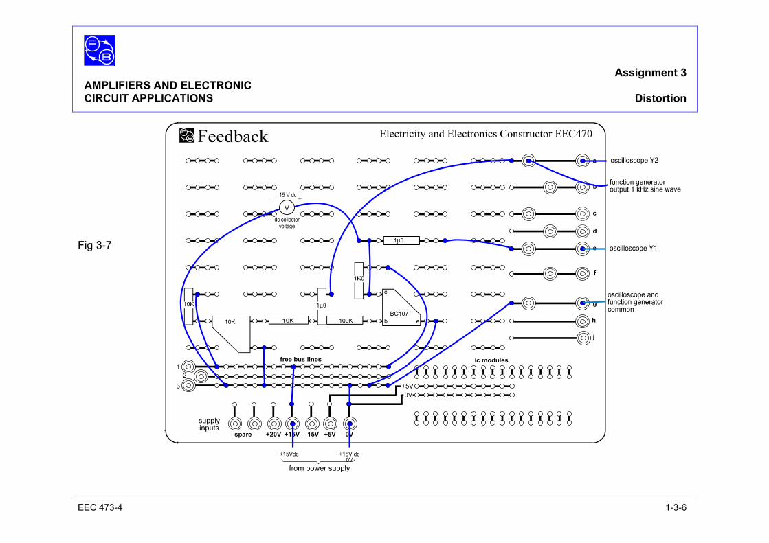
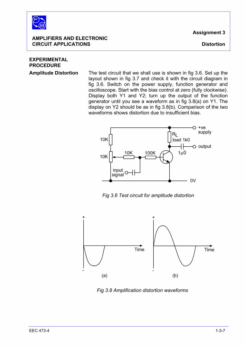
EXPERIMENTAL PROCEDURE Amplitude Distortion The test circuit that we shall use is shown in fig 3.6. Set up the
layout shown in fig 3.7 and check it with the circuit diagram in fig 3.6. Switch on the power supply, function generator and oscilloscope. Start with the bias control at zero (fully clockwise). Display both Y1 and Y2; turn up the output of the function generator until you see a waveform as in fig 3.8(a) on Y1. The display on Y2 should be as in fig 3.8(b). Comparison of the two waveforms shows distortion due to insufficient bias.
Fig 3.6 Test circuit for amplitude distortion
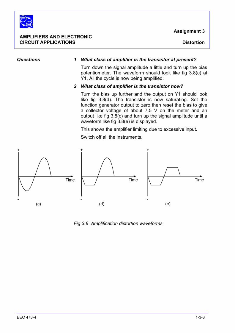
Fig 3.8 Amplification distortion waveforms
Assignment 3 AMPLIFIERS AND ELECTRONIC CIRCUIT APPLICATIONS Distortion
EEC 473-4 1-3-8
Questions 1 What class of amplifier is the transistor at present? Turn down the signal amplitude a little and turn up the bias potentiometer. The waveform should look like fig 3.8(c) at Y1. All the cycle is now being amplified.
2 What class of amplifier is the transistor now? Turn the bias up further and the output on Y1 should look
like fig 3.8(d). The transistor is now saturating. Set the function generator output to zero then reset the bias to give a collector voltage of about 7.5 V on the meter and an output like fig 3.8(c) and turn up the signal amplitude until a waveform like fig 3.8(e) is displayed.
This shows the amplifier limiting due to excessive input. Switch off all the instruments.
Fig 3.8 Amplification distortion waveforms
Assignment 3 AMPLIFIERS AND ELECTRONIC CIRCUIT APPLICATIONS Distortion
EEC 473-4 1-3-9
Variation of Gain with Signal Amplitude In this activity we shall demonstrate the variation of gain with
signal amplitude. Using the same test circuit, set the bias potentiometer for a
collector voltage of 8 volts on the meter. Set the function generator to triangle wave output. Turn up the
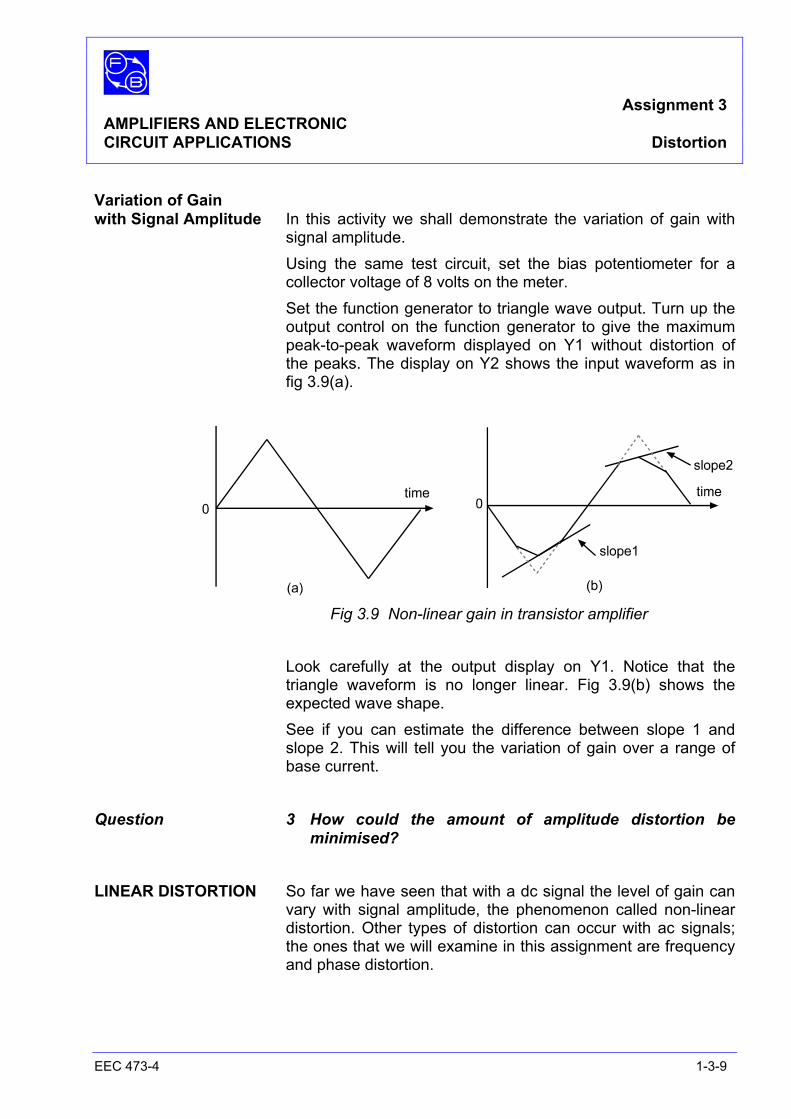
output control on the function generator to give the maximum peak-to-peak waveform displayed on Y1 without distortion of the peaks. The display on Y2 shows the input waveform as in fig 3.9(a).
Fig 3.9 Non-linear gain in transistor amplifier Look carefully at the output display on Y1. Notice that the
triangle waveform is no longer linear. Fig 3.9(b) shows the expected wave shape.
See if you can estimate the difference between slope 1 and slope 2. This will tell you the variation of gain over a range of base current.
Question 3 How could the amount of amplitude distortion be minimised?
LINEAR DISTORTION So far we have seen that with a dc signal the level of gain can vary with signal amplitude, the phenomenon called non-linear distortion. Other types of distortion can occur with ac signals; the ones that we will examine in this assignment are frequency and phase distortion.
Assignment 3 AMPLIFIERS AND ELECTRONIC CIRCUIT APPLICATIONS Distortion
EEC 473-4 1-3-10
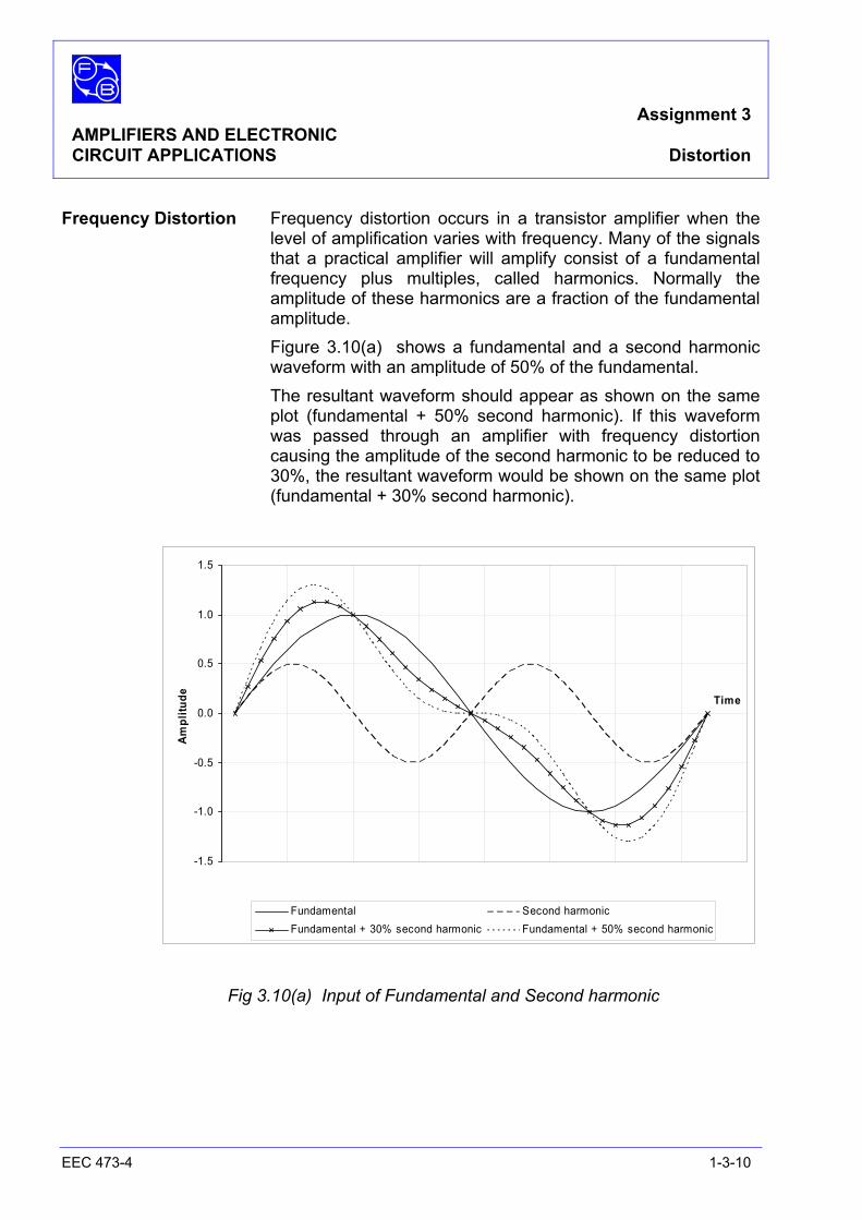
Frequency Distortion Frequency distortion occurs in a transistor amplifier when the level of amplification varies with frequency. Many of the signals that a practical amplifier will amplify consist of a fundamental frequency plus multiples, called harmonics. Normally the amplitude of these harmonics are a fraction of the fundamental amplitude.
Figure 3.10(a) shows a fundamental and a second harmonic waveform with an amplitude of 50% of the fundamental.
The resultant waveform should appear as shown on the same plot (fundamental + 50% second harmonic). If this waveform was passed through an amplifier with frequency distortion causing the amplitude of the second harmonic to be reduced to 30%, the resultant waveform would be shown on the same plot (fundamental + 30% second harmonic).
-1.5
-1.0
-0.5
0.0
0.5
1.0
1.5
Time
Am
plitu
de
Fundamental Second harmonicFundamental + 30% second harmonic Fundamental + 50% second harmonic
Fig 3.10(a) Input of Fundamental and Second harmonic
Assignment 3 AMPLIFIERS AND ELECTRONIC CIRCUIT APPLICATIONS Distortion
EEC 473-4 1-3-11
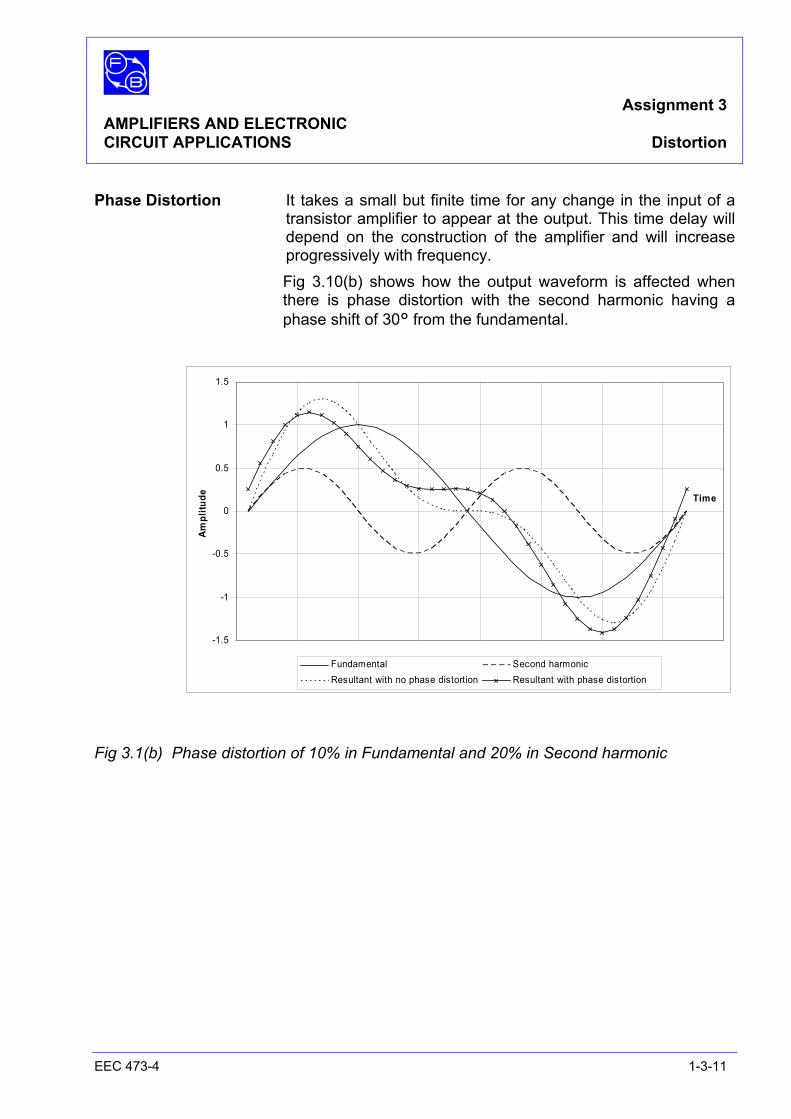
Phase Distortion It takes a small but finite time for any change in the input of a transistor amplifier to appear at the output. This time delay will depend on the construction of the amplifier and will increase progressively with frequency. Fig 3.10(b) shows how the output waveform is affected when there is phase distortion with the second harmonic having a phase shift of 30° from the fundamental.
-1.5
-1
-0.5
0
0.5
1
1.5
Time
Am
plitu
de
Fundamental Second harmonicResultant with no phase distortion Resultant with phase distortion
Fig 3.1(b) Phase distortion of 10% in Fundamental and 20% in Second harmonic
Assignment 3 AMPLIFIERS AND ELECTRONIC CIRCUIT APPLICATIONS Distortion
EEC 473-4 1-3-12
The Practical Amplifier A practical amplifier will have a combination of frequency and phase distortion together with amplitude distortion.
In most applications, such as in audio amplification, unless the distortion is severe it will not affect the operation of the system.
Demonstrating and Measuring Distortion The laboratory function generator is a good instrument for
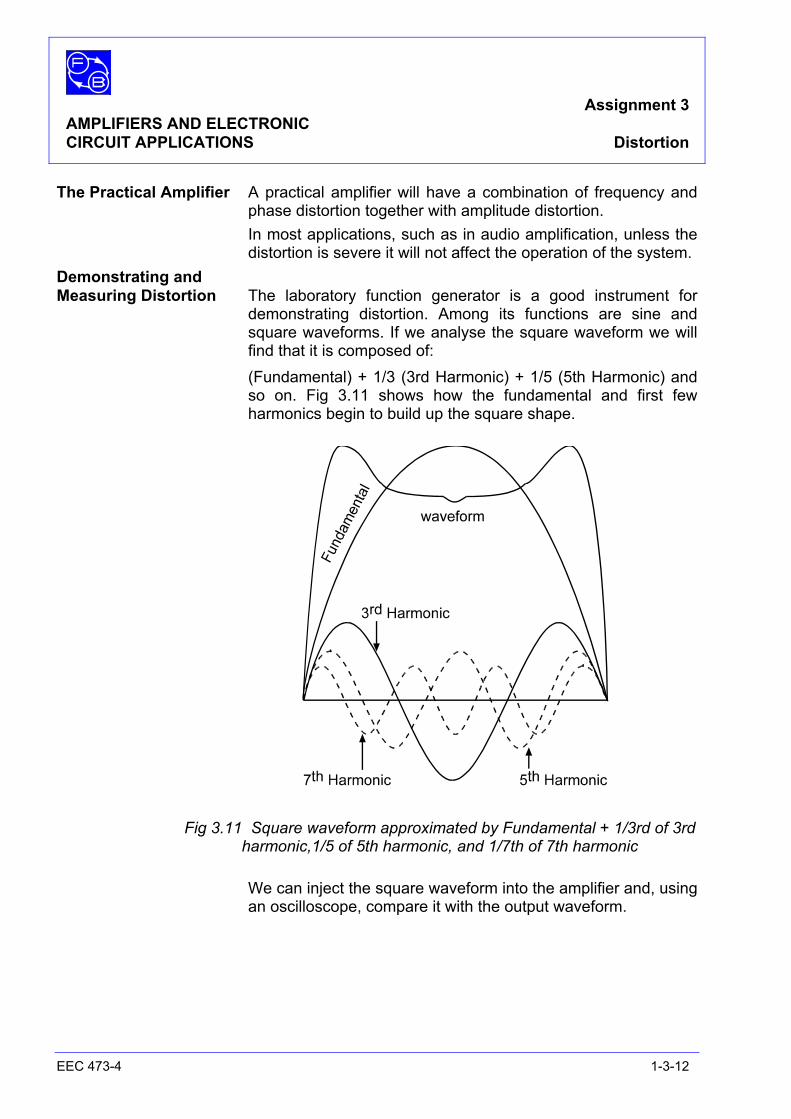
demonstrating distortion. Among its functions are sine and square waveforms. If we analyse the square waveform we will find that it is composed of:
(Fundamental) + 1/3 (3rd Harmonic) + 1/5 (5th Harmonic) and so on. Fig 3.11 shows how the fundamental and first few harmonics begin to build up the square shape.
Fig 3.11 Square waveform approximated by Fundamental + 1/3rd of 3rd
harmonic,1/5 of 5th harmonic, and 1/7th of 7th harmonic We can inject the square waveform into the amplifier and, using
an oscilloscope, compare it with the output waveform.

Ass
ignm
ent 3
A
MPL
IFIE
RS
AN
D E
LEC
TRO
NIC
CIR
CU
IT A
PPLI
CA
TIO
NS
Dis
tort
ion
EE
C 4
73-4
1-
3-13
Not
es
Assignment 3 AMPLIFIERS AND ELECTRONIC CIRCUIT APPLICATIONS Distortion
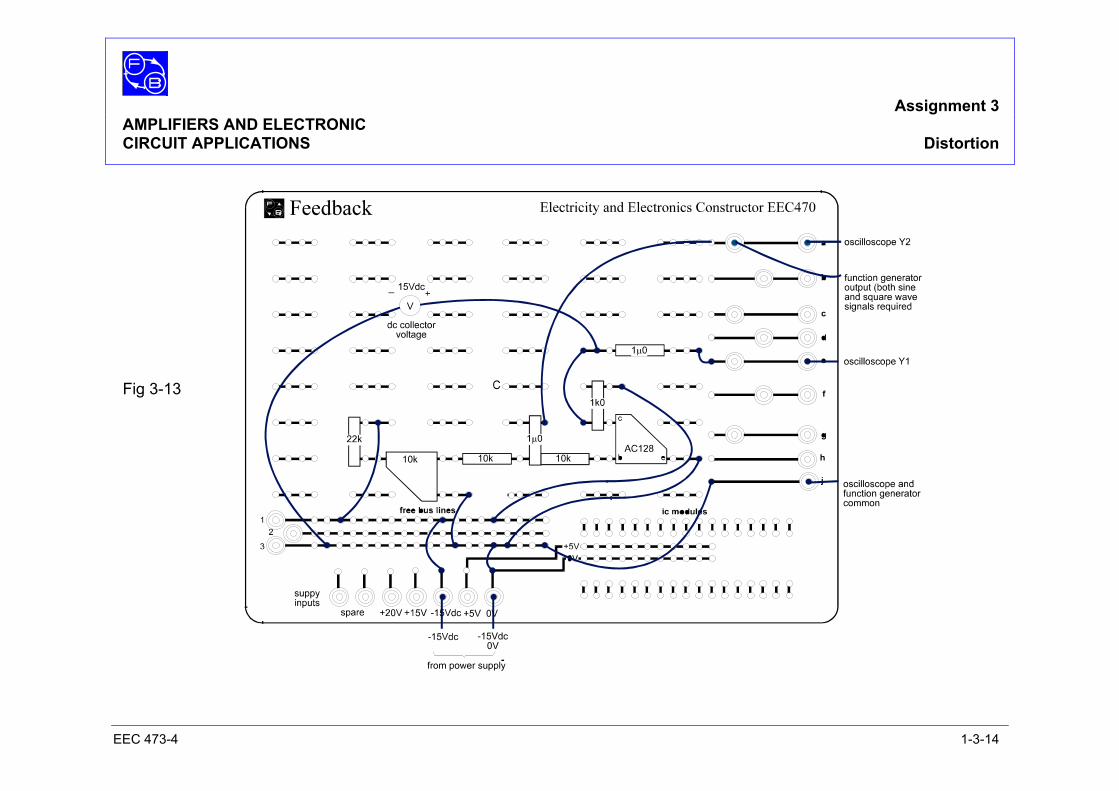
EEC 473-4 1-3-14
Fig 3-13
Assignment 3 AMPLIFIERS AND ELECTRONIC CIRCUIT APPLICATIONS Distortion
EEC 473-4 1-3-15
EXPERIMENTAL PROCEDURE Firstly we shall compare the amplifier performance with square
waves of different frequencies. Secondly we shall analyse the effect of a square wave by seeing if the harmonics have the same degree of amplification as the fundamental and measure the amount of phase difference between input and output.
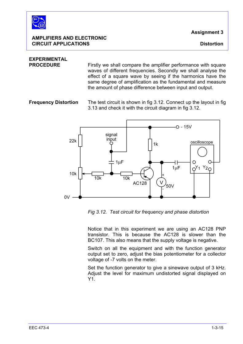
Frequency Distortion The test circuit is shown in fig 3.12. Connect up the layout in fig
3.13 and check it with the circuit diagram in fig 3.12.
Fig 3.12. Test circuit for frequency and phase distortion
Notice that in this experiment we are using an AC128 PNP transistor. This is because the AC128 is slower than the BC107. This also means that the supply voltage is negative.
Switch on all the equipment and with the function generator output set to zero, adjust the bias potentiometer for a collector voltage of -7 volts on the meter.
Set the function generator to give a sinewave output of 3 kHz. Adjust the level for maximum undistorted signal displayed on Y1.
Assignment 3 AMPLIFIERS AND ELECTRONIC CIRCUIT APPLICATIONS Distortion
EEC 473-4 1-3-16
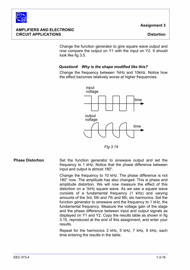
Change the function generator to give square wave output and now compare the output on Y1 with the input on Y2. It should look like fig 3.5.
Question4 Why is the shape modified like this?
Change the frequency between 1kHz and 10kHz. Notice how the effect becomes relatively worse at higher frequencies.
inputvoltage
outputvoltage
time
time
Fig 3.14
Phase Distortion Set the function generator to sinewave output and set the frequency to 1 kHz. Notice that the phase difference between input and output is almost 180°.
Change the frequency to 10 kHz. The phase difference is not 180° now. The amplitude has also changed. This is phase and amplitude distortion. We will now measure the effect of this distortion on a 1kHz square wave. As we saw a square wave consists of a fundamental frequency (1 kHz) and varying amounts of the 3rd, 5th and 7th and 9th, etc harmonics. Set the function generator to sinewave and the frequency to 1 kHz, the fundamental frequency. Measure the voltage gain of the stage and the phase difference between input and output signals as displayed on Y1 and Y2. Copy the results table as shown in fig 3.15, reproduced at the end of this assignment, and enter your results.
Repeat for the harmonics 3 kHz, 5 kHz, 7 kHz, 9 kHz, each time entering the results in the table.
Assignment 3 AMPLIFIERS AND ELECTRONIC CIRCUIT APPLICATIONS Distortion
EEC 473-4 1-3-17
If we call the comparative stage gain at the fundamental frequency, unity (1), then all the other values will be less than one; ie, a fraction of the gain at the fundamental. If we call the phase change between input and output zero at the fundamental, the other phase angles will be the difference between the change at the harmonic and the change at the fundamental.
Make a new table with these comparative values like fig 3.17. By looking at the table you have made you can see the effect of
frequency and phase distortion.
Assignment 3 AMPLIFIERS AND ELECTRONIC CIRCUIT APPLICATIONS Distortion
EEC 473-4 1-3-18
PRACTICAL CONSIDERATIONS AND APPLICATIONS The human ear has a considerable tolerance to changes in
intensity. It considers sound to be twice as loud when in fact it has increased by ten times.
An amplifier operating a control valve in a chemical plant is far more exacting in its requirements, a small error may cause an explosion.
There are methods for making amplifiers more linear and in the following assignments we shall examine ways of achieving this.
Ageing does increase the amount of distortion, so it is important to check equipment in a systematic way. By doing this and replacing components as distortion increases, the incidence of total failure can be reduced.
Signal distortion is a problem. We have seen that it is a combination of several factors. An added problem can be coupling between connecting leads. This is why coaxial or screened leads are often used in electronic equipment, particularly where high gain amplifiers are used at high frequency. By using his knowledge of amplifier distortion the maintenance engineer can often diagnose a fault by examining the input and output waveforms of a system.
In audio systems mainly the amplitude change with frequency is important, because luckily the ear is not easily able to detect phase changes. This makes the design of hi-fi audio amplifiers a little easier.
SUMMARY In this assignment you have learnt that:
1 The transistor amplifier is non-linear 2 Improper bias setting will produce a large amount of
distortion 3 Too large an input signal will also produce a large amount
of distortion. 4. Complex wave shapes, like square waves, are composed
of a fundamental and harmonic frequencies together. 5. Frequency distortion occurs when the amplification at
different frequencies is not the same. 6. Phase distortion occurs when the phase change between
input and output at different frequencies is not the same.
Assignment 3 AMPLIFIERS AND ELECTRONIC CIRCUIT APPLICATIONS Distortion
EEC 473-4 1-3-19
7. Problems can occur when there is coupling between nearby wires. This can be prevented by using screened cable.
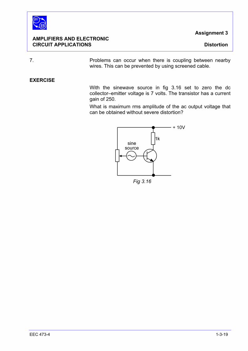
EXERCISE With the sinewave source in fig 3.16 set to zero the dc
collector–emitter voltage is 7 volts. The transistor has a current gain of 250.
What is maximum rms amplitude of the ac output voltage that can be obtained without severe distortion?
Fig 3.16
Assignment 3 AMPLIFIERS AND ELECTRONIC CIRCUIT APPLICATIONS Distortion
EEC 473-4 1-3-20
Notes
Assignment 3 AMPLIFIERS AND ELECTRONIC CIRCUIT APPLICATIONS Answers and Results
EEC 473-4 1-3-21
ANSWERS TO ASSIGNMENT 3 1 The amplifier is operating in Class B, as only the positive
parts of the input signal are being amplified. 2 The amplifier is operating in class A, as all the input signal
is being amplified. 3 The distortion could be minimised by using the amplifier at
the lowest possible input level, hence keeping the variation of gain to a minimum.
4 As we said the amplification decreases as the frequency increases. The sharp edge of the square wave requires the amplification of the high frequencies. As the amplification is low at high frequency the sharp edge is modified to a curve.
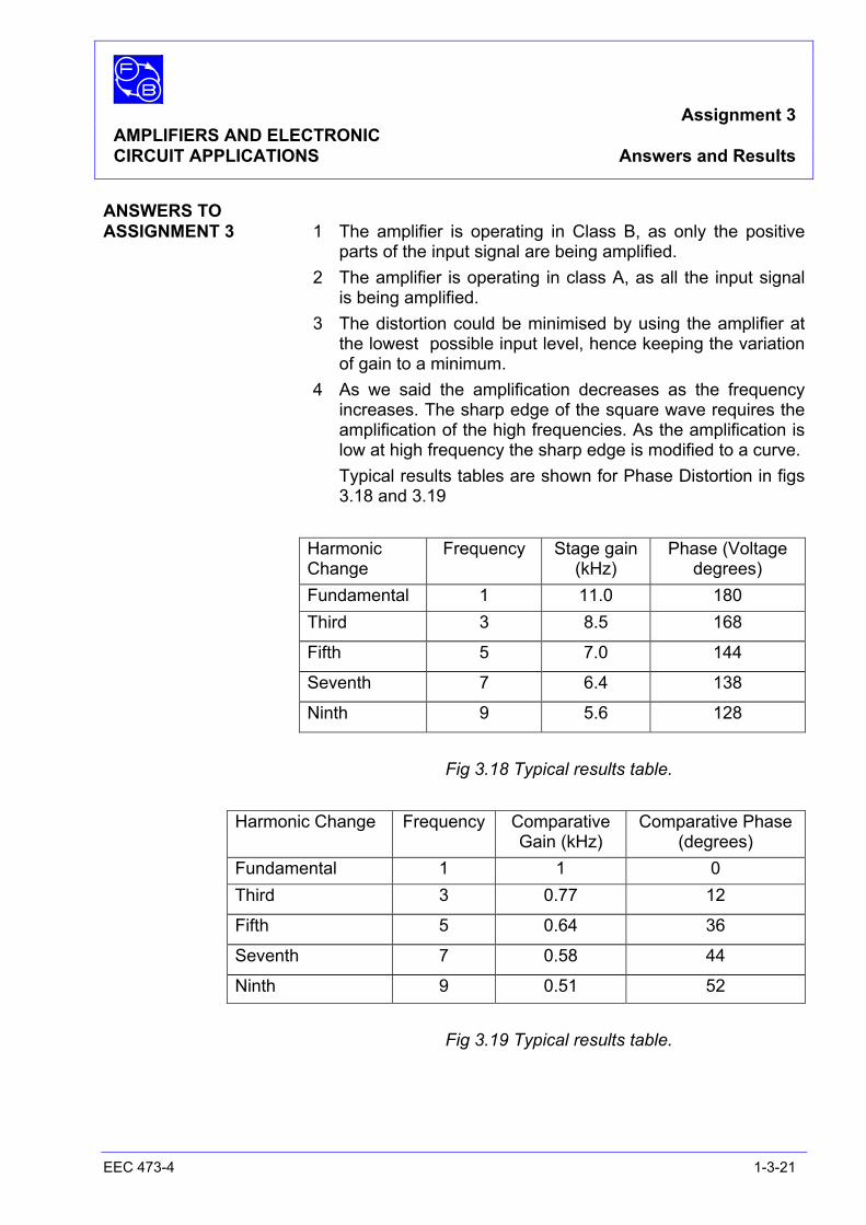
Typical results tables are shown for Phase Distortion in figs 3.18 and 3.19
Harmonic Change
Frequency Stage gain (kHz)
Phase (Voltage degrees)
Fundamental 1 11.0 180 Third 3 8.5 168
Fifth 5 7.0 144
Seventh 7 6.4 138
Ninth 9 5.6 128
Fig 3.18 Typical results table.
Harmonic Change Frequency Comparative
Gain (kHz) Comparative Phase
(degrees) Fundamental 1 1 0 Third 3 0.77 12
Fifth 5 0.64 36
Seventh 7 0.58 44
Ninth 9 0.51 52
Fig 3.19 Typical results table.
Assignment 3 AMPLIFIERS AND ELECTRONIC CIRCUIT APPLICATIONS Answers and Results
EEC 473-4 1-3-22
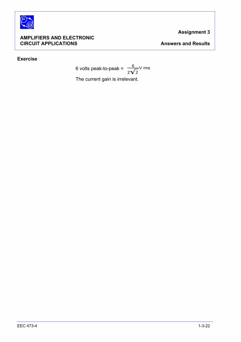
Exercise
6 volts peak-to-peak = 62 2
V rms
The current gain is irrelevant.
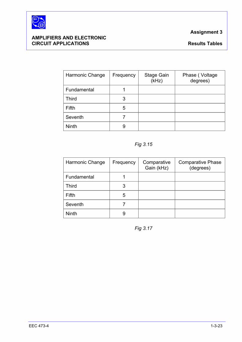
Assignment 3 AMPLIFIERS AND ELECTRONIC CIRCUIT APPLICATIONS Results Tables
EEC 473-4 1-3-23
Harmonic Change Frequency Stage Gain (kHz)
Phase ( Voltage degrees)
Fundamental 1
Third 3
Fifth 5
Seventh 7
Ninth 9
Fig 3.15
Harmonic Change Frequency Comparative Gain (kHz)
Comparative Phase (degrees)
Fundamental 1
Third 3
Fifth 5
Seventh 7
Ninth 9
Fig 3.17

Assignment 3 AMPLIFIERS AND ELECTRONIC CIRCUIT APPLICATIONS Results Tables
EEC 473-4 1-3-24
Notes
Assignment 4 AMPLIFIERS AND ELECTRONIC CIRCUIT APPLICATIONS Negative Feedback
EEC 473-4 1-4-1
OBJECTIVES 1. To observe the effect of negative feedback on the voltage gain and input impedance of an amplifier.
2. To understand the use of negative feedback in the emitter follower amplifier.
EQUIPMENT REQUIRED Qty Apparatus 1 Electricity & Electronics Constructor
EEC470 1 Amplifier Kit EEC473-4 1 Power supply unit +15 V dc regulated (eg, Feedback Power Supply 92-445 or
optionally the 92-100 Teknikit console) 1 2–Channel oscilloscope 1 Function generator. Sinusoidal 5 V pk-to-pk
@ 1 kHz (eg, Feedback FG601 ) 1 Multimeter or 1 Voltmeter 15 V dc
PREREQUISITE ASSIGNMENTS Assignment 3
KNOWLEDGE LEVEL See Prerequisite Assignments

Assignment 4 AMPLIFIERS AND ELECTRONIC CIRCUIT APPLICATIONS Negative Feedback
EEC 473-4 1-4-2
Notes
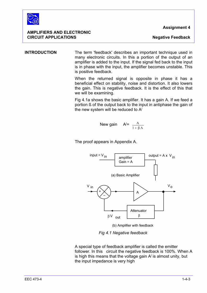
Assignment 4 AMPLIFIERS AND ELECTRONIC CIRCUIT APPLICATIONS Negative Feedback
EEC 473-4 1-4-3
INTRODUCTION The term 'feedback' describes an important technique used in many electronic circuits. In this a portion of the output of an amplifier is added to the input. If the signal fed back to the input is in phase with the input, the amplifier becomes unstable. This is positive feedback.
When the returned signal is opposite in phase it has a beneficial effect on stability, noise and distortion. It also lowers the gain. This is negative feedback. It is the effect of this that we will be examining.
Fig 4.1a shows the basic amplifier. It has a gain A. If we feed a portion ß of the output back to the input in antiphase the gain of the new system will be reduced to A/
New gain A/= AA1 + β
The proof appears in Appendix A.
Fig 4.1 Negative feedback A special type of feedback amplifier is called the emitter
follower. In this circuit the negative feedback is 100%. When A is high this means that the voltage gain A/ is almost unity, but the input impedance is very high
Assignment 4 AMPLIFIERS AND ELECTRONIC CIRCUIT APPLICATIONS Negative Feedback
EEC 473-4 1-4-4
We will find out the effect of negative feedback on gain and device input impedance in an amplifier using a high-gain transistor, the BC107, and a low-gain transistor, the BSX20, of the emitter follower circuit.

Ass
ignm
ent 4
A
MPL
IFIE
RS
AN
D E
LEC
TRO
NIC
CIR
CU
IT A
PPLI
CA
TIO
NS
Neg
ativ
e Fe
edba
ck
473-
4 1-
4-5
Not
es
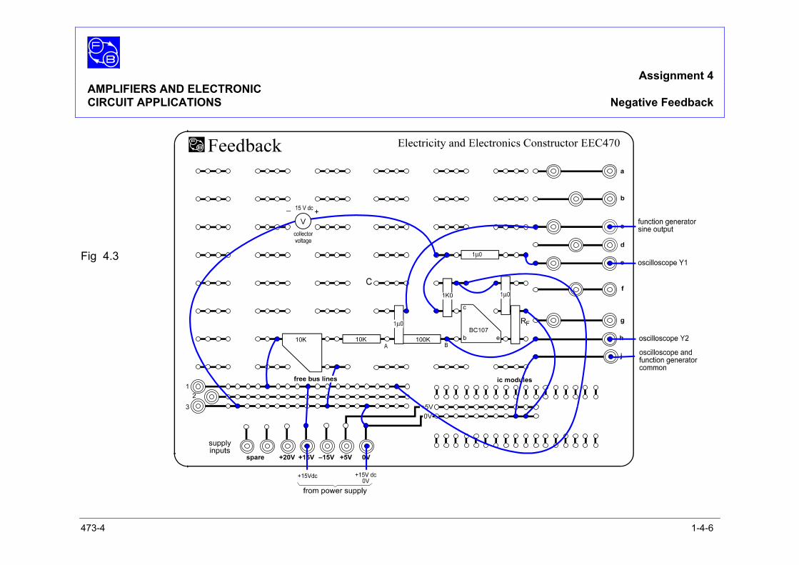
Assignment 4 AMPLIFIERS AND ELECTRONIC CIRCUIT APPLICATIONS Negative Feedback
473-4 1-4-6
Fig 4.3
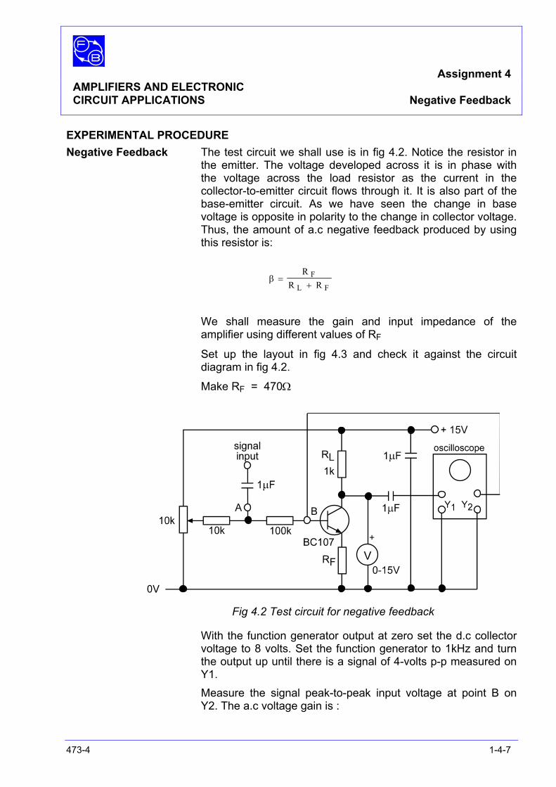
Assignment 4 AMPLIFIERS AND ELECTRONIC CIRCUIT APPLICATIONS Negative Feedback
473-4 1-4-7
EXPERIMENTAL PROCEDURE Negative Feedback The test circuit we shall use is in fig 4.2. Notice the resistor in
the emitter. The voltage developed across it is in phase with the voltage across the load resistor as the current in the collector-to-emitter circuit flows through it. It is also part of the base-emitter circuit. As we have seen the change in base voltage is opposite in polarity to the change in collector voltage. Thus, the amount of a.c negative feedback produced by using this resistor is:
β =+
RR R
F
L F
We shall measure the gain and input impedance of the amplifier using different values of RF
Set up the layout in fig 4.3 and check it against the circuit diagram in fig 4.2.
Make RF = 470Ω
Fig 4.2 Test circuit for negative feedback
With the function generator output at zero set the d.c collector voltage to 8 volts. Set the function generator to 1kHz and turn the output up until there is a signal of 4-volts p-p measured on Y1.
Measure the signal peak-to-peak input voltage at point B on Y2. The a.c voltage gain is :
Assignment 4 AMPLIFIERS AND ELECTRONIC CIRCUIT APPLICATIONS Negative Feedback
473-4 1-4-8
voltage input a.c. peaktopeakvoltage output a.c. peaktopeak
−−−−
Copy the results table as shown in fig 4.4, reproduced at the end of this assignment, and enter the value in the appropriate place.
Now we need to find the input impedance. Measure the ac peak-to-peak voltage at A by moving the Y2 input from point B to A. From the voltage drop across the resistor we can find the input resistance by using the formula
V
V VB
A B−x 100 kΩ = Rin
we can calculate the ac input impedance. Enter the value in the
table. Repeat for the other values of RF in the table of fig 4.4. Questions 1 How does the gain and input impedance vary
with the amount of negative feedback?
Enter in the values of RR
L
F in the table.
Repeat the experiment using the lower gain BSX20 transistor.
Look carefully at the results. Answer the following questions:
2 When a large amount of negative feedback is used, how much effect does the gain of the transistor have on the gain of the amplifier?
3 What other effect does the use of a low-gain transistor have on the circuit?
4 When the gain of the transistor is large compared with the amount of negative feedback being used, is the ratio of collector resistance to emitter resistance significant?
5 If an amplifier has a high input impedance what does this say about the current gain?
Assignment 4 AMPLIFIERS AND ELECTRONIC CIRCUIT APPLICATIONS Negative Feedback
473-4 1-4-9
Emitter Follower In this activity we will investigate the emitter follower. Make the following changes to the circuit: 1 Switch off power supply 2 Remove RL and replace it by a wire link
3 Connect the Y1 input of the oscilloscope via the 1 µF capacitor to the junction of RF and the emitter of the transistor. Connect the meter to the same point.
4 Replace the transistor by a BC107. Check that your layout agrees with the test circuit diagram in fig
4.5.
Make RF = 470 Ω.
Switch on the power supply and set the bias to maximum. The d.c emitter voltage should be about 3 volts. Turn up the function generator output until an output on Y1 of 2.5 volts peak-to-peak of signal occurs. Notice that the output is in phase with the input. The voltage gain is unity.
Using the method described earlier in the Assignment, measure the input impedance.
Change the value of RF to 100 Ω. Notice that the voltage gain is still unity.
Check again the input impedance. Compare these values with those obtained previously for the simple negative feedback circuit, fig 4.2.
Fig 4.5 Test circuit for emitter follower
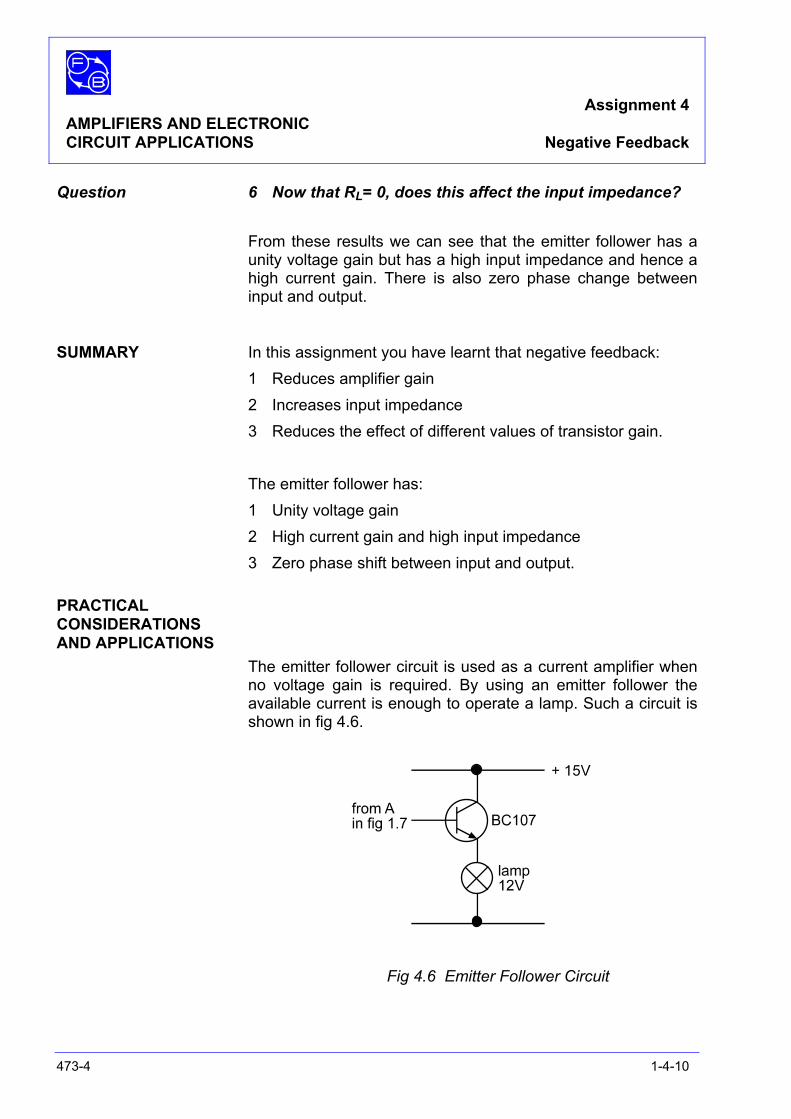
Assignment 4 AMPLIFIERS AND ELECTRONIC CIRCUIT APPLICATIONS Negative Feedback
473-4 1-4-10
Question 6 Now that RL= 0, does this affect the input impedance? From these results we can see that the emitter follower has a
unity voltage gain but has a high input impedance and hence a high current gain. There is also zero phase change between input and output.
SUMMARY In this assignment you have learnt that negative feedback: 1 Reduces amplifier gain 2 Increases input impedance 3 Reduces the effect of different values of transistor gain. The emitter follower has: 1 Unity voltage gain 2 High current gain and high input impedance 3 Zero phase shift between input and output. PRACTICAL CONSIDERATIONS AND APPLICATIONS The emitter follower circuit is used as a current amplifier when
no voltage gain is required. By using an emitter follower the available current is enough to operate a lamp. Such a circuit is shown in fig 4.6.
Fig 4.6 Emitter Follower Circuit
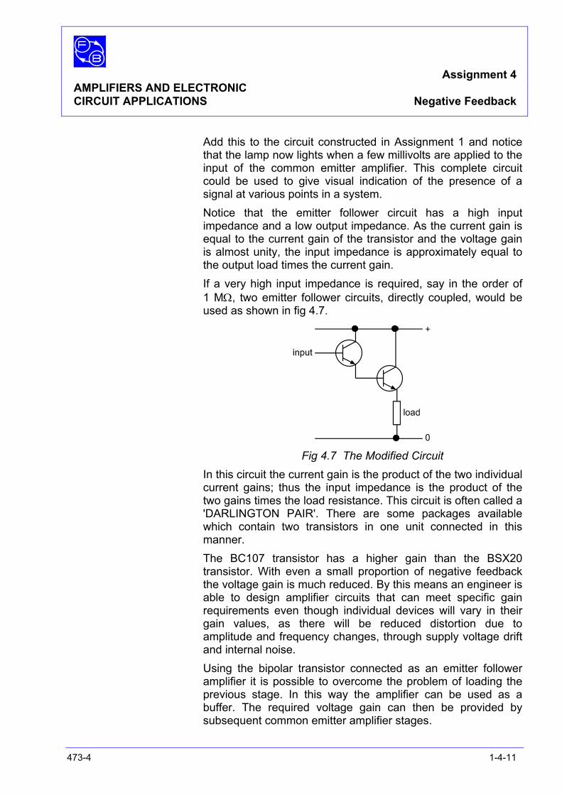
Assignment 4 AMPLIFIERS AND ELECTRONIC CIRCUIT APPLICATIONS Negative Feedback
473-4 1-4-11
Add this to the circuit constructed in Assignment 1 and notice that the lamp now lights when a few millivolts are applied to the input of the common emitter amplifier. This complete circuit could be used to give visual indication of the presence of a signal at various points in a system.
Notice that the emitter follower circuit has a high input impedance and a low output impedance. As the current gain is equal to the current gain of the transistor and the voltage gain is almost unity, the input impedance is approximately equal to the output load times the current gain.
If a very high input impedance is required, say in the order of 1 MΩ, two emitter follower circuits, directly coupled, would be used as shown in fig 4.7.
Fig 4.7 The Modified Circuit
In this circuit the current gain is the product of the two individual current gains; thus the input impedance is the product of the two gains times the load resistance. This circuit is often called a 'DARLINGTON PAIR'. There are some packages available which contain two transistors in one unit connected in this manner.
The BC107 transistor has a higher gain than the BSX20 transistor. With even a small proportion of negative feedback the voltage gain is much reduced. By this means an engineer is able to design amplifier circuits that can meet specific gain requirements even though individual devices will vary in their gain values, as there will be reduced distortion due to amplitude and frequency changes, through supply voltage drift and internal noise.
Using the bipolar transistor connected as an emitter follower amplifier it is possible to overcome the problem of loading the previous stage. In this way the amplifier can be used as a buffer. The required voltage gain can then be provided by subsequent common emitter amplifier stages.
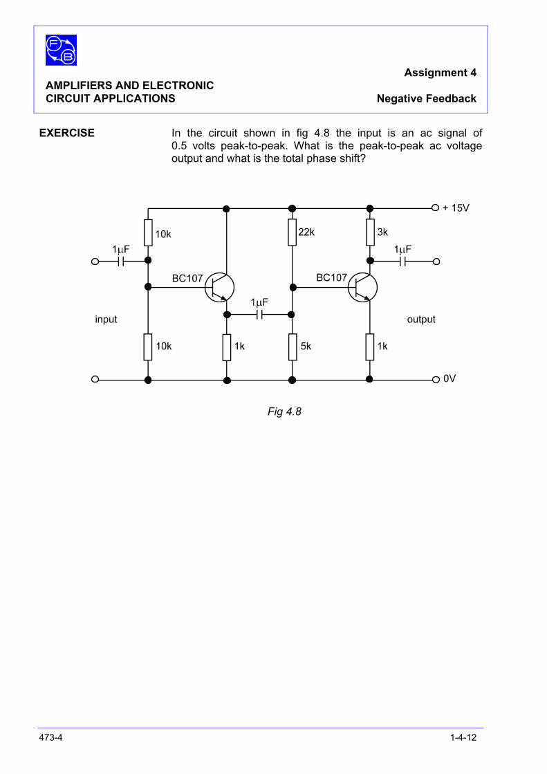
Assignment 4 AMPLIFIERS AND ELECTRONIC CIRCUIT APPLICATIONS Negative Feedback
473-4 1-4-12
EXERCISE In the circuit shown in fig 4.8 the input is an ac signal of 0.5 volts peak-to-peak. What is the peak-to-peak ac voltage output and what is the total phase shift?
Fig 4.8
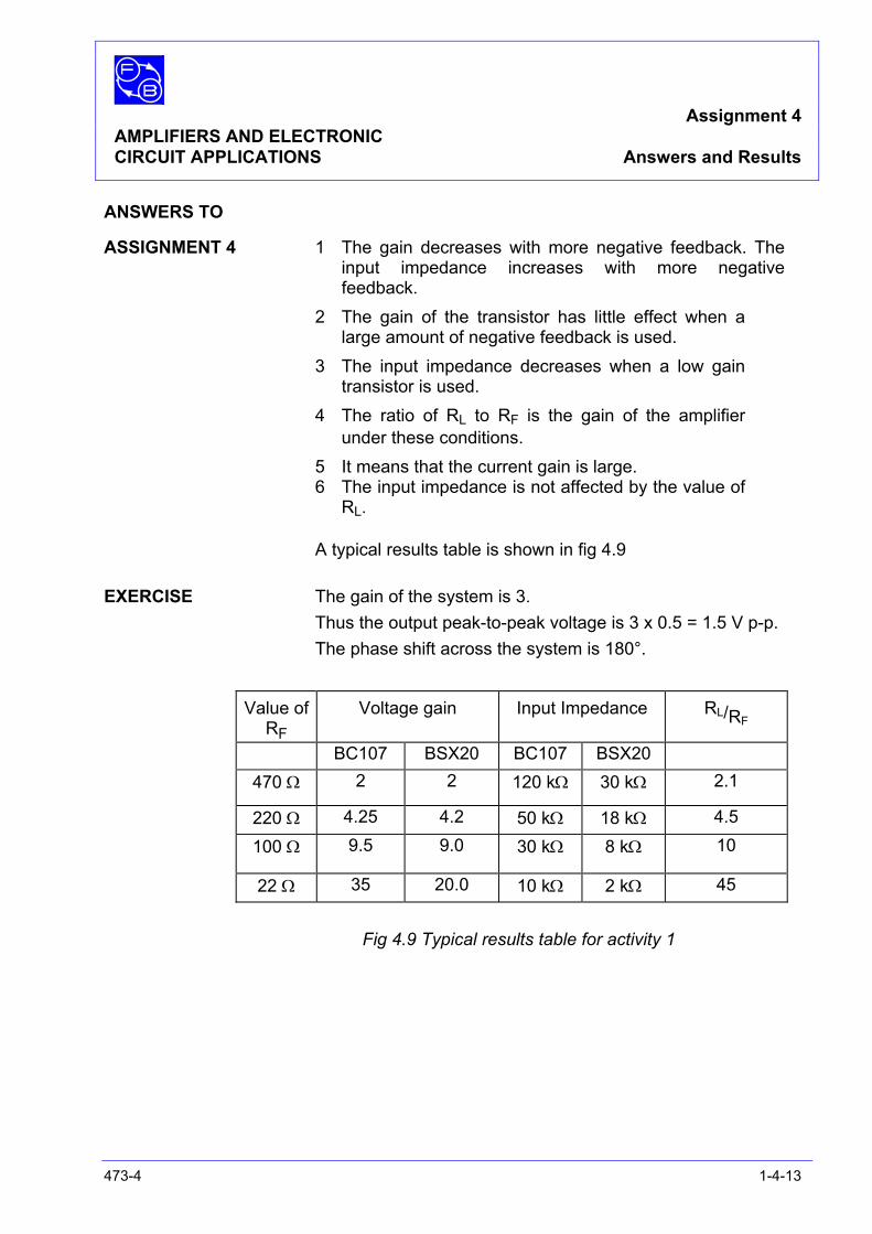
Assignment 4 AMPLIFIERS AND ELECTRONIC CIRCUIT APPLICATIONS Answers and Results
473-4 1-4-13
ANSWERS TO
ASSIGNMENT 4 1 The gain decreases with more negative feedback. The input impedance increases with more negative feedback.
2 The gain of the transistor has little effect when a large amount of negative feedback is used.
3 The input impedance decreases when a low gain transistor is used.
4 The ratio of RL to RF is the gain of the amplifier under these conditions.
5 It means that the current gain is large. 6 The input impedance is not affected by the value of
RL. A typical results table is shown in fig 4.9 EXERCISE The gain of the system is 3. Thus the output peak-to-peak voltage is 3 x 0.5 = 1.5 V p-p. The phase shift across the system is 180°.
Value of RF
Voltage gain Input Impedance RL/RF
BC107 BSX20 BC107 BSX20 470 Ω 2 2 120 kΩ 30 kΩ 2.1
220 Ω 4.25 4.2 50 kΩ 18 kΩ 4.5
100 Ω 9.5 9.0 30 kΩ 8 kΩ 10
22 Ω 35 20.0 10 kΩ 2 kΩ 45
Fig 4.9 Typical results table for activity 1
Assignment 4 AMPLIFIERS AND ELECTRONIC CIRCUIT APPLICATIONS Answers and Results
473-4 1-4-14
Notes
Assignment 4 AMPLIFIERS AND ELECTRONIC CIRCUIT APPLICATIONS Results Table
473-4 1-4-15
Value of RF
Voltage gain Input Impedance RL/RF
BC107 BSX20 BC107 BSX20 470 Ω
220 Ω
100 Ω
22 Ω Fig 4.4

Assignment 4 AMPLIFIERS AND ELECTRONIC CIRCUIT APPLICATIONS Results Table
473-4 1-4-16
Notes
Assignment 5 AMPLIFIERS AND ELECTRONIC CIRCUIT APPLICATIONS Frequency Response
473-4 1-5-1
OBJECTIVES 1 To understand the meaning of frequency response, gain and phase shift in an amplifier.
2 To understand the effect of negative feedback on frequency response, gain and phase shift.
EQUIPMENT REQUIRED Qty Apparatus 1 Electricity & Electronics Constructor
EEC470 1 Amplifier Kit EEC473-4 1 Power supply unit –15 V dc regulated (eg, Feedback Power
Supply 92-445 or optionally the 92-100 Teknikit console)
1 Function generator Sinusoidal 5 V pk-to-pk @ 100 kHz (eg, Feedback FG601 )
1 2–Channel oscilloscope 1 Multimeter or 1 Voltmeter 15 V dc
PREREQUISITE ASSIGNMENTS Assignment 4
KNOWLEDGE LEVEL See prerequisite requirements
Assignment 5 AMPLIFIERS AND ELECTRONIC CIRCUIT APPLICATIONS Frequency Response
EEC 473-4 1-5-2
Notes
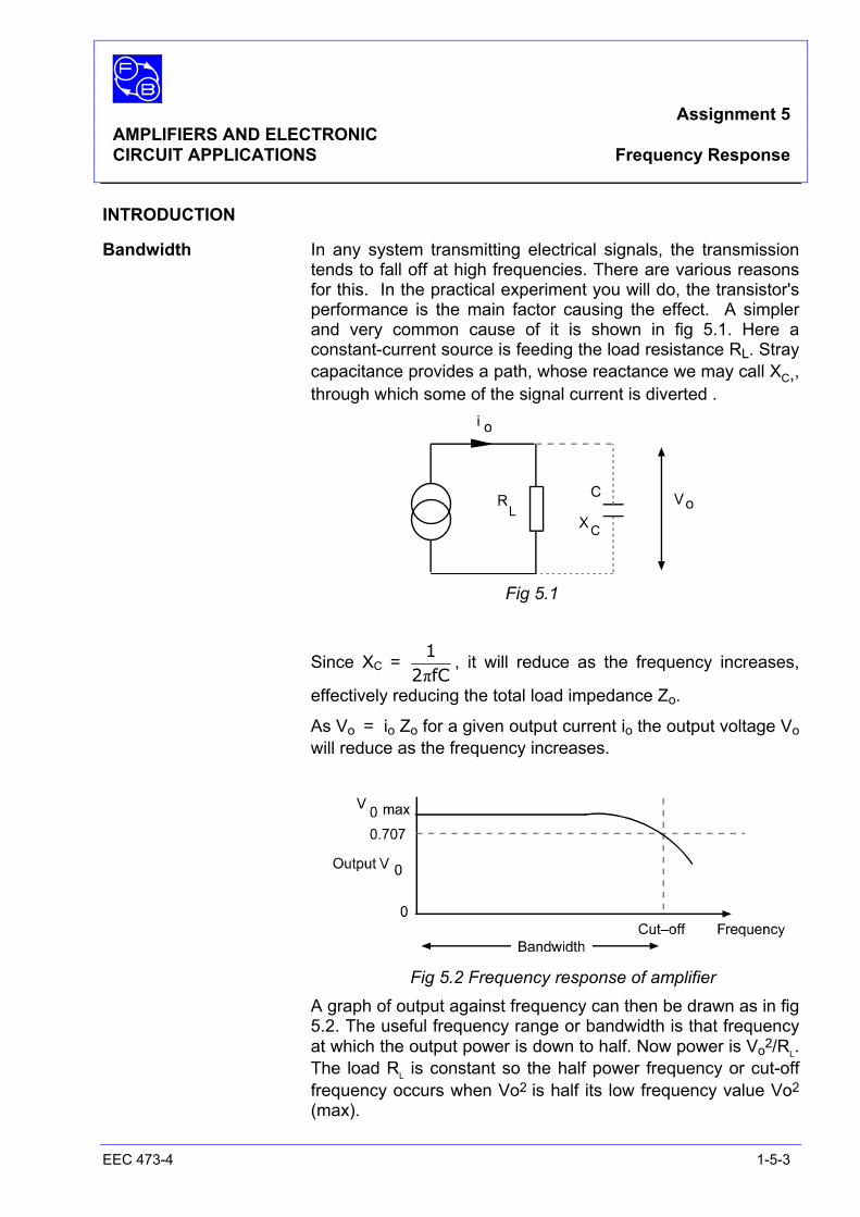
Assignment 5 AMPLIFIERS AND ELECTRONIC CIRCUIT APPLICATIONS Frequency Response
EEC 473-4 1-5-3
INTRODUCTION
Bandwidth In any system transmitting electrical signals, the transmission tends to fall off at high frequencies. There are various reasons for this. In the practical experiment you will do, the transistor's performance is the main factor causing the effect. A simpler and very common cause of it is shown in fig 5.1. Here a constant-current source is feeding the load resistance RL. Stray capacitance provides a path, whose reactance we may call XC,, through which some of the signal current is diverted .
Fig 5.1
Since XC = fC21π
, it will reduce as the frequency increases,
effectively reducing the total load impedance Zo.
As Vo = io Zo for a given output current io the output voltage Vo will reduce as the frequency increases.
Fig 5.2 Frequency response of amplifier A graph of output against frequency can then be drawn as in fig
5.2. The useful frequency range or bandwidth is that frequency at which the output power is down to half. Now power is Vo2/RL. The load RL is constant so the half power frequency or cut-off frequency occurs when Vo2 is half its low frequency value Vo2 (max).
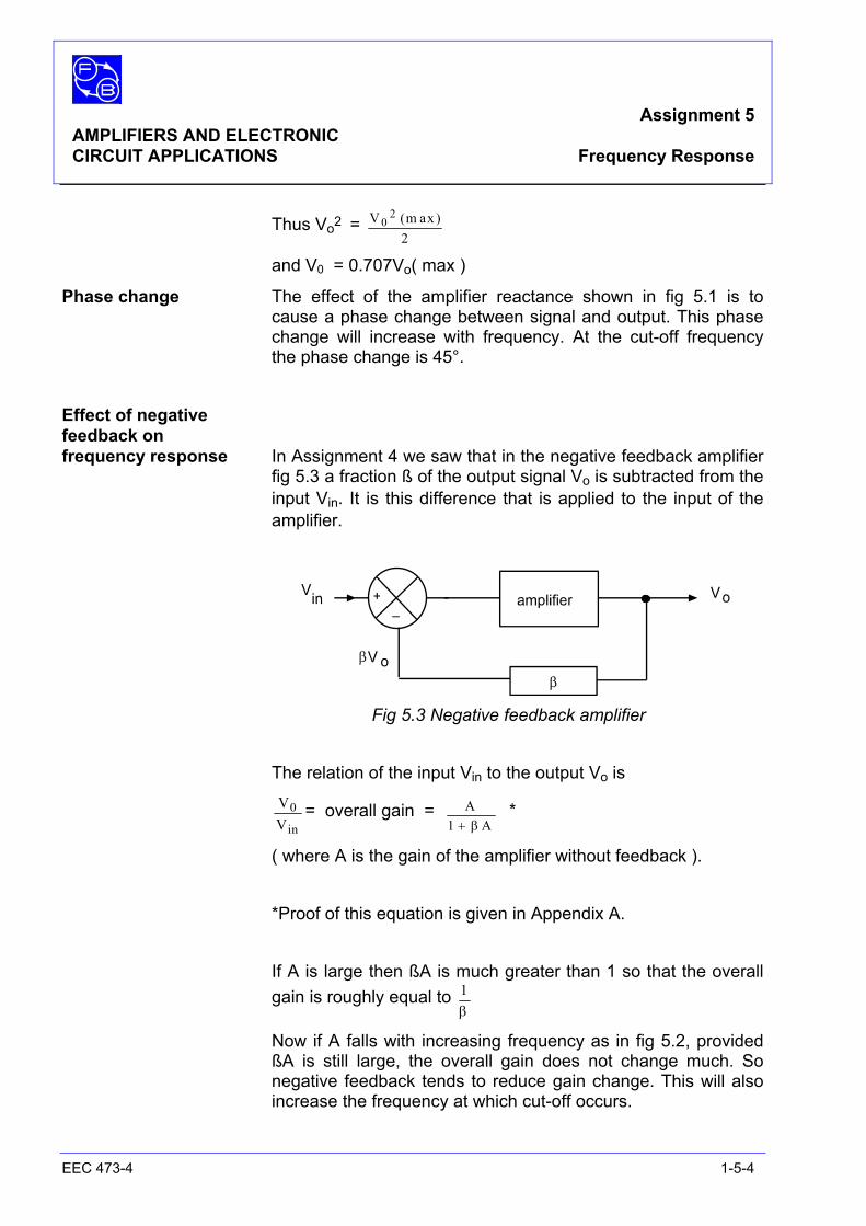
Assignment 5 AMPLIFIERS AND ELECTRONIC CIRCUIT APPLICATIONS Frequency Response
EEC 473-4 1-5-4
Thus Vo2 = V 02
2(m ax )
and V0 = 0.707Vo( max )
Phase change The effect of the amplifier reactance shown in fig 5.1 is to cause a phase change between signal and output. This phase change will increase with frequency. At the cut-off frequency the phase change is 45°.
Effect of negative feedback on frequency response In Assignment 4 we saw that in the negative feedback amplifier
fig 5.3 a fraction ß of the output signal Vo is subtracted from the input Vin. It is this difference that is applied to the input of the amplifier.
Fig 5.3 Negative feedback amplifier The relation of the input Vin to the output Vo is
VVin
0 = overall gain = AA1 + β
*
( where A is the gain of the amplifier without feedback ). *Proof of this equation is given in Appendix A. If A is large then ßA is much greater than 1 so that the overall
gain is roughly equal to 1β
Now if A falls with increasing frequency as in fig 5.2, provided ßA is still large, the overall gain does not change much. So negative feedback tends to reduce gain change. This will also increase the frequency at which cut-off occurs.
Assignment 5 AMPLIFIERS AND ELECTRONIC CIRCUIT APPLICATIONS Frequency Response
EEC 473-4 1-5-5
Effect of negative feedback on phase lag The same reasoning can be applied to the effect of negative
feedback on phase lag as applied to gain. For a given frequency the phase lag with negative feedback will be less than without it.
General effect of negative feedback If the output changes for any reason, the negative feedback
affects the input in such a way as to counteract the change.

Assignment 5 AMPLIFIERS AND ELECTRONIC CIRCUIT APPLICATIONS Frequency Response
EEC 473-4 1-5-6
Notes

Ass
ignm
ent 5
A
MPL
IFIE
RS
AN
D E
LEC
TRO
NIC
CIR
CU
IT A
PPLI
CA
TIO
NS
Freq
uenc
y R
espo
nse
473-
4 1-
5-7
Not
es
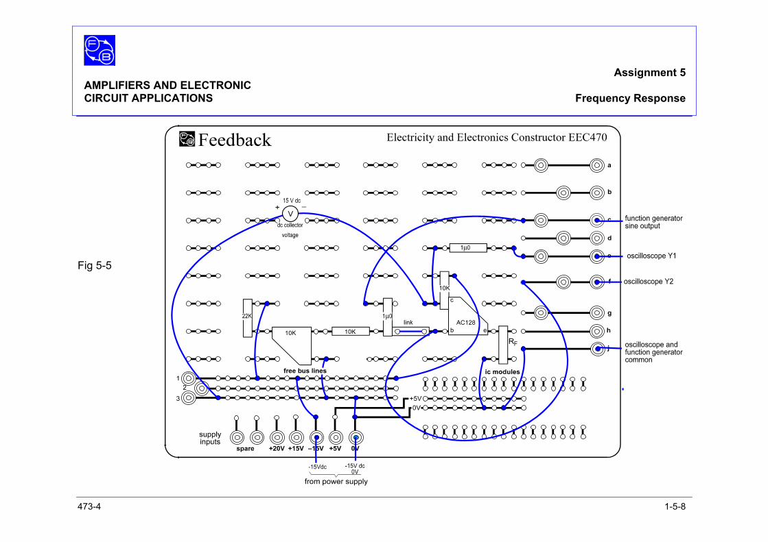
Assignment 5 AMPLIFIERS AND ELECTRONIC CIRCUIT APPLICATIONS Frequency Response
473-4 1-5-8
Fig 5-5
Assignment 5 AMPLIFIERS AND ELECTRONIC CIRCUIT APPLICATIONS Frequency Response
EEC 473-4 1-5-9
EXPERIMENTAL PROCEDURE Frequency Response In this activity we shall measure the gain of a transistor
amplifier at various frequencies comparing the response with and without negative feedback. The transistor used is the PNP AC128, and the feedback introduced by adding a resistor in the emitter circuit.
Fig 5.4 Test circuit for frequency response The test circuit is shown in fig 5.4. Set up the layout in fig 5.5 and check it against the test circuit
in fig 5.4. Make RF = 0 by inserting a link. Set the function generator frequency to 1 kHz. With the function generator output set to zero, set the dc
collector voltage to 8 volts as shown on the voltmeter using the 10 kΩ potentiometer. Turn up the function generator output until there is an 8-volt peak-to-peak signal displayed on Y1. Monitor the input on Y2. It will be quite small.
Measure the voltage gain:
voltage base peaktopeak
voltage collector peaktopeak−−
−−
Assignment 5 AMPLIFIERS AND ELECTRONIC CIRCUIT APPLICATIONS Frequency Response
EEC 473-4 1-5-10
Copy the results table as shown in fig 5.6, reproduced at the end of this assignment, and enter the value.
Measure the gain at the other frequencies in the table entering the results in the gain column.
Notice the gain reduction at high frequencies.
Assignment 5 AMPLIFIERS AND ELECTRONIC CIRCUIT APPLICATIONS Frequency Response
EEC 473-4 1-5-11
Question 1 Calculate the percentage gain reduction between 1 kHz and 100 kHz.
% reduction = kHz) 1 at (gain
kHz) 100 at (gain-kHz)1at(gain
Now add some negative feedback by removing the emitter link
and replacing it by a 220-ohm resistor. Repeat the gain measurements, and enter the results in your table.
Question 2 What is the percentage gain reduction between 1 kHz and 100 kHz now the feedback has been added?
Phase Change Using the same test circuit we shall now measure the phase change between input and output of the amplifier with and without negative feedback. Replace RF with the wire link again. Set the function generator to 1 kHz and measure the phase difference between Y1 and Y2 waveforms on the oscilloscope. Record the value in your table.
Measure the phase change for the other frequencies on the table and enter the values.
Now replace the link with a 220 Ω resistor as before and repeat the phase change measurements. When you have entered all the values in the table consider what they tell you about the circuit.
Question 3 What effect has the addition of negative feedback had on the phase shift of the amplifier?
Assignment 5 AMPLIFIERS AND ELECTRONIC CIRCUIT APPLICATIONS Frequency Response
EEC 473-4 1-5-12
PRACTICAL CONSIDERATIONS AND APPLICATIONS In the experiment, the negative feedback was proportional to
the current in the transistor. This feedback tended to stabilise that current against the effects of changing frequency. Note however that if extra capacitance had been put in parallel with the load, worsening the drop in high-frequency response, the feedback signal would not have been affected, and so the feedback would have no effect on the loss of high frequencies from this cause. (To correct this, a feedback signal proportional to the output voltage would have been required.)
Negative feedback plays an important part in the design and
stabilisation of amplifier circuits. Where noise is introduced internally the feedback can be applied between the output and point just before the origin of the noise. The noise is then reduced by the feedback but the gain of the earlier stages can be increased. Thus noise can be reduced by using negative feedback.
It also allows amplifiers to be produced having a fixed level of gain over a wide bandwidth and offsets variation in device characteristics.
SUMMARY In this assignment you have learnt that: 1 The bandwidth of an amplifier is the frequency range in
which the gain is within 70.7% of the maximum. 2 At cut-off the phase change compared with the phase
change at maximum gain is 45°. 3 By using negative feedback the bandwidth can be
extended. 4 By using negative feedback the phase change occurring
with frequency is reduced.
EXERCISE Refer back to Assignment 4 and calculate the value of ß, the feedback fraction, for the amplifier in this assignment.
Now choose a frequency in the results table and by taking the voltage gain with and without feedback, calculate the practical value of ß. See if it agrees with the theory.
Assignment 5 AMPLIFIERS AND ELECTRONIC CIRCUIT APPLICATIONS Answers and Results
EEC 473-4 1-5-13
ANSWERS TO ASSIGNMENT 5 All answers refer to the typical results table, fig 5.7.
Frequency Voltage gain Phase change (degrees)
RF= 0 RF=220 Ω RF = 0 RF=220 Ω
1kHz 200 40 180 180 5kHz 200 40 180° 180° 10kHz 190 40 190 180 30kHz 190 40 200 185 60kHz 180 35 210 190
100kHz 125 30 250 210 Fig 5.7. Typical results table . 1 37.5% 2 25% 3 The phase shift has been reduced by using negative
feedback.
Exercise The value of ß is
β =+
RR R
F
L F= 2 2 0
1 0 2 2 0k + = 0.021
From the formula:
A/= AA1 + β
where ß= A − AA A
/
/
At 1 kHz : 2 0 0 4 02 0 0 4 0
−x
= 0.02
The practical value is very close to the theoretical value in this case.

Assignment 5 AMPLIFIERS AND ELECTRONIC CIRCUIT APPLICATIONS Answers and Results
EEC 473-4 1-5-14
Notes
Assignment 5 AMPLIFIERS AND ELECTRONIC CIRCUIT APPLICATIONS Results Tables
EEC 473-4 1-5-15
Frequency Voltage gain Phase change (degrees)
RF= 0 RF=220 Ω RF = 0 RF=220 Ω
1 kHz 5 kHz 10 kHz 30 kHz 60 kHz
100 kHz Fig 5.6.

Assignment 5 AMPLIFIERS AND ELECTRONIC CIRCUIT APPLICATIONS Results Tables
EEC 473-4 1-5-16
Notes
Assignment 6 AMPLIFIERS AND ELECTRONIC CIRCUIT APPLICATIONS The ac Amplifier
EEC 473-4 1-6-1
OBJECTIVES 1 An understanding of automatic bias and the use of the by- pass capacitor. 2 An understanding of inductive coupling and
impedance matching.
EQUIPMENT REQUIRED Qty Apparatus 1 Electricity & Electronics Constructor EEC470 1 Amplifier Kit EEC473-4 1 Power supply unit +15 V dc regulated (eg, Feedback Power Supply 92-445 or optionally the 92-100 Teknikit Console) 1 Function generator 1 2–Channel oscilloscope 1 Multimeter or 1 Voltmeter 15 V dc.
PREREQUISITE ASSIGNMENTS Assignment 5
KNOWLEDGE LEVEL See prerequisite assignments

Assignment 6 AMPLIFIERS AND ELECTRONIC CIRCUIT APPLICATIONS The ac Amplifier
EEC 473-4 1-6-2
Notes
Assignment 6 AMPLIFIERS AND ELECTRONIC CIRCUIT APPLICATIONS The ac Amplifier
EEC 473-4 1-6-3
INTRODUCTION The aim of the ac amplifier is to amplify ac signals and block dc signals. In order to achieve amplification with minimum distortion, the bias point of the transistor must be controlled carefully.
Fig 6.1
Use of Automatic Biasing and By-pass Capacitor With the biasing arrangement of fig 6.1(a), if there is any
change in the supply voltage then the voltage on the base will alter.
The bias voltage can be stabilised by placing resistor RE in the emitter circuit as in fig 6.1(b). Now if, say, the supply voltage Vcc increases, the collector current Ic also increases. The voltage across RE also increases and the voltage on the base relative to the emitter VBE is lowered, thus reducing the base current. The collector current is then reduced and so the circuit tends to be stabilised at a fixed level.
As RE is a feedback resistor, it will reduce the amplifier gain. This is overcome by placing a large by-pass capacitor CE across RE. Over the operating range of frequencies, the capacitor's reactance will be extremely low, there will be little ac feedback effect and good ac gain. Below the operating range the reactance will increase, there will be an ac negative feedback effect and the gain will be reduced.
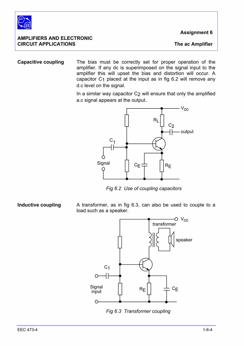
Assignment 6 AMPLIFIERS AND ELECTRONIC CIRCUIT APPLICATIONS The ac Amplifier
EEC 473-4 1-6-4
Capacitive coupling The bias must be correctly set for proper operation of the amplifier. If any dc is superimposed on the signal input to the amplifier this will upset the bias and distortion will occur. A capacitor C1 placed at the input as in fig 6.2 will remove any d.c level on the signal.
In a similar way capacitor C2 will ensure that only the amplified a.c signal appears at the output.
Fig 6.2 Use of coupling capacitors
Inductive coupling A transformer, as in fig 6.3, can also be used to couple to a load such as a speaker.
Fig 6.3 Transformer coupling
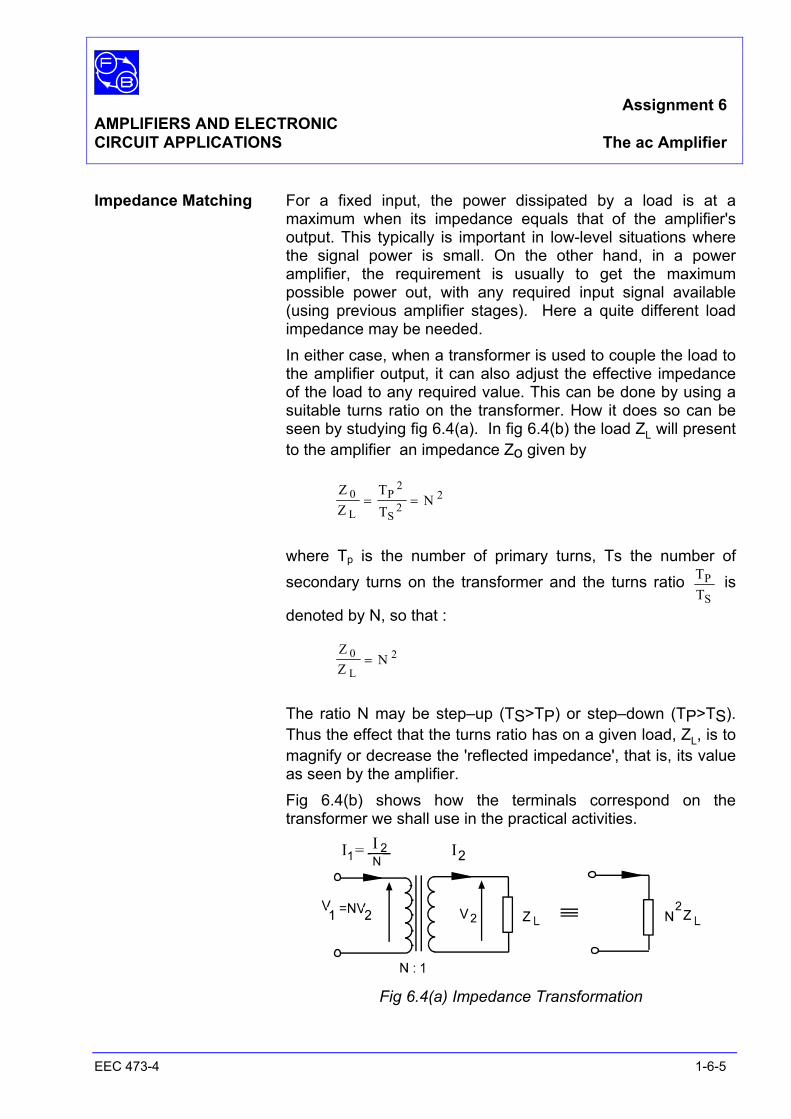
Assignment 6 AMPLIFIERS AND ELECTRONIC CIRCUIT APPLICATIONS The ac Amplifier
EEC 473-4 1-6-5
Impedance Matching For a fixed input, the power dissipated by a load is at a maximum when its impedance equals that of the amplifier's output. This typically is important in low-level situations where the signal power is small. On the other hand, in a power amplifier, the requirement is usually to get the maximum possible power out, with any required input signal available (using previous amplifier stages). Here a quite different load impedance may be needed.
In either case, when a transformer is used to couple the load to the amplifier output, it can also adjust the effective impedance of the load to any required value. This can be done by using a suitable turns ratio on the transformer. How it does so can be seen by studying fig 6.4(a). In fig 6.4(b) the load ZL will present to the amplifier an impedance Zo given by
ZZ
TT
NL
P
S
02
22= =
where Tp is the number of primary turns, Ts the number of secondary turns on the transformer and the turns ratio T
TP
S is
denoted by N, so that :
ZZ
NL
0 2=
The ratio N may be step–up (TS>TP) or step–down (TP>TS). Thus the effect that the turns ratio has on a given load, ZL, is to magnify or decrease the 'reflected impedance', that is, its value as seen by the amplifier.
Fig 6.4(b) shows how the terminals correspond on the transformer we shall use in the practical activities.
Fig 6.4(a) Impedance Transformation
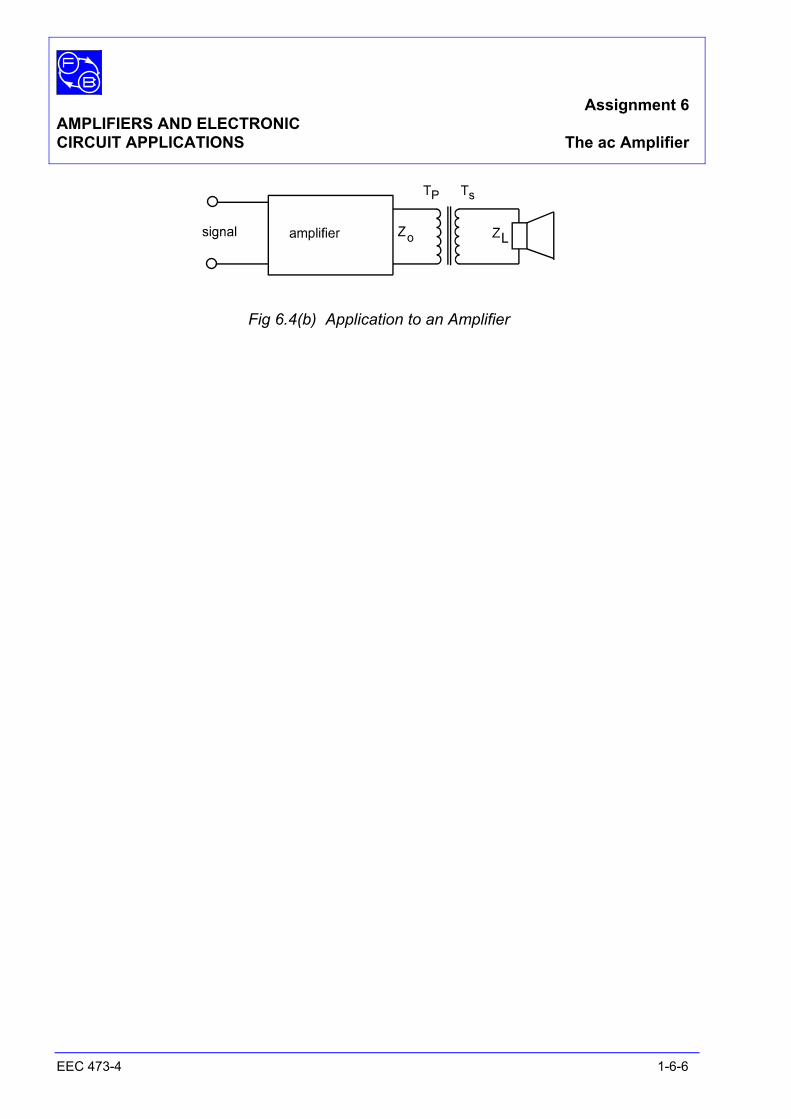
Assignment 6 AMPLIFIERS AND ELECTRONIC CIRCUIT APPLICATIONS The ac Amplifier
EEC 473-4 1-6-6
Fig 6.4(b) Application to an Amplifier

Ass
ignm
ent 6
A
MPL
IFIE
RS
AN
D E
LEC
TRO
NIC
CIR
CU
IT A
PPLI
CA
TIO
NS
The
ac A
mpl
ifier
E
EC
473
-4
1-6-
7
Not
es
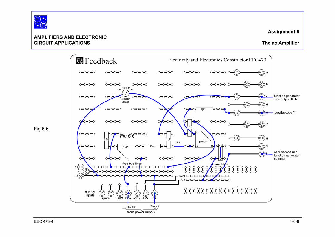
Assignment 6 AMPLIFIERS AND ELECTRONIC CIRCUIT APPLICATIONS The ac Amplifier
EEC 473-4 1-6-8
Fig 6-6 Fig 6.6
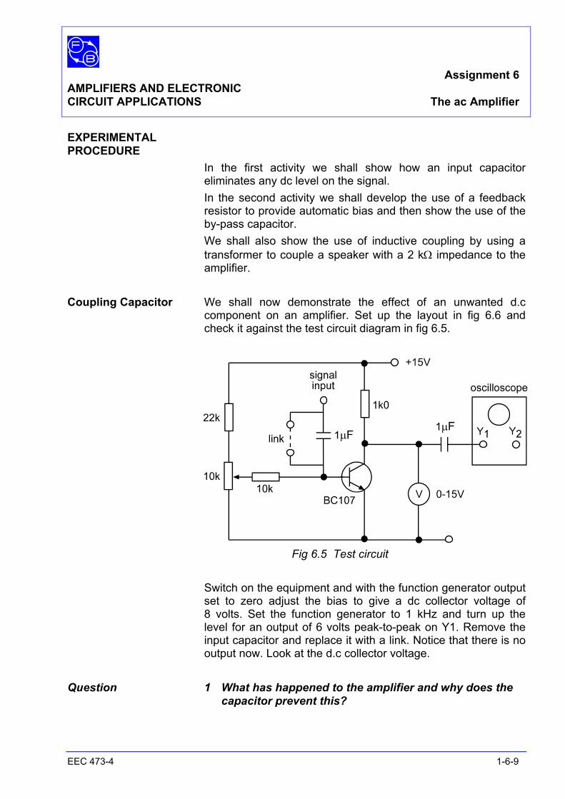
Assignment 6 AMPLIFIERS AND ELECTRONIC CIRCUIT APPLICATIONS The ac Amplifier
EEC 473-4 1-6-9
EXPERIMENTAL PROCEDURE In the first activity we shall show how an input capacitor
eliminates any dc level on the signal. In the second activity we shall develop the use of a feedback
resistor to provide automatic bias and then show the use of the by-pass capacitor.
We shall also show the use of inductive coupling by using a transformer to couple a speaker with a 2 kΩ impedance to the amplifier.
Coupling Capacitor We shall now demonstrate the effect of an unwanted d.c
component on an amplifier. Set up the layout in fig 6.6 and check it against the test circuit diagram in fig 6.5.
Fig 6.5 Test circuit Switch on the equipment and with the function generator output
set to zero adjust the bias to give a dc collector voltage of 8 volts. Set the function generator to 1 kHz and turn up the level for an output of 6 volts peak-to-peak on Y1. Remove the input capacitor and replace it with a link. Notice that there is no output now. Look at the d.c collector voltage.
Question 1 What has happened to the amplifier and why does the
capacitor prevent this?
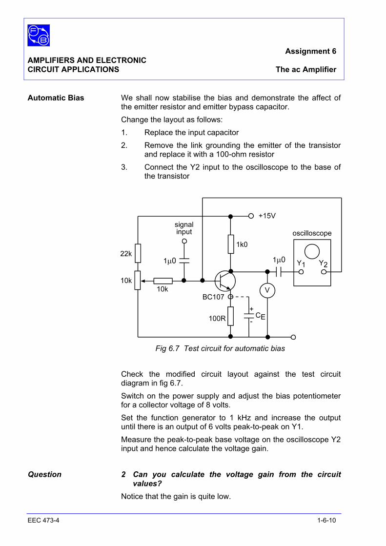
Assignment 6 AMPLIFIERS AND ELECTRONIC CIRCUIT APPLICATIONS The ac Amplifier
EEC 473-4 1-6-10
Automatic Bias We shall now stabilise the bias and demonstrate the affect of the emitter resistor and emitter bypass capacitor.
Change the layout as follows: 1. Replace the input capacitor 2. Remove the link grounding the emitter of the transistor
and replace it with a 100-ohm resistor 3. Connect the Y2 input to the oscilloscope to the base of
the transistor
Fig 6.7 Test circuit for automatic bias Check the modified circuit layout against the test circuit
diagram in fig 6.7. Switch on the power supply and adjust the bias potentiometer
for a collector voltage of 8 volts. Set the function generator to 1 kHz and increase the output
until there is an output of 6 volts peak-to-peak on Y1. Measure the peak-to-peak base voltage on the oscilloscope Y2
input and hence calculate the voltage gain.
Question 2 Can you calculate the voltage gain from the circuit values?
Notice that the gain is quite low.
Assignment 6 AMPLIFIERS AND ELECTRONIC CIRCUIT APPLICATIONS The ac Amplifier
EEC 473-4 1-6-11
Turn the bias potentiometer up and down, notice that the collector voltage can vary by quite a large amount before distortion is introduced. The bias has now been automatically stabilised.
Return the bias potentiometer to the original position for a collector voltage of 8 volts. Now add a 100 µF capacitor in parallel with the emitter resistor. Notice that the capacitor has a positive and negative end. Make sure that the negative end is connected to ground or the capacitor will not work properly.
Reduce the function generator output until the waveform shows no distortion.
Measure the voltage gain with the capacitor in circuit. It is now much larger. Compare it with the voltage gain in the
previous assignment when no negative feedback was used. It is quite near that value.
Turn the bias potentiometer again up and down and notice that the action has not been changed by adding the by-pass capacitor.
Questions 3 Do you think that the ac distortion, noise, ac input impedance and phase distortion performance is near that of an amplifier with or without negative feedback?
Try other capacitor values as emitter by-pass. Use a 1 µF and a 0.22 µF capacitor.
4 What happens when the size of the capacitor is reduced?

Assignment 6 AMPLIFIERS AND ELECTRONIC CIRCUIT APPLICATIONS The ac Amplifier
EEC 473-4 1-6-12
Notes

Ass
ignm
ent 6
A
MPL
IFIE
RS
AN
D E
LEC
TRO
NIC
CIR
CU
IT A
PPLI
CA
TIO
NS
The
ac A
mpl
ifier
E
EC
473
-4
1-6-
13
Not
es
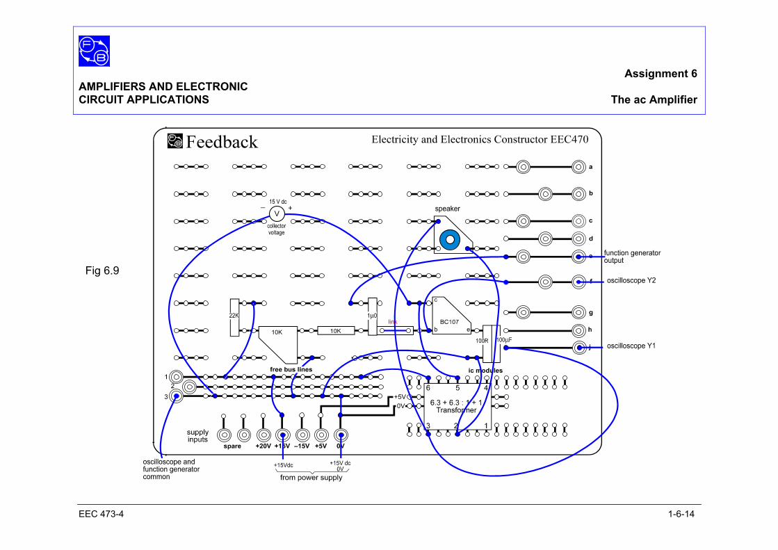
Assignment 6 AMPLIFIERS AND ELECTRONIC CIRCUIT APPLICATIONS The ac Amplifier
EEC 473-4 1-6-14
Fig 6.9
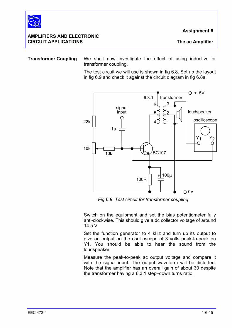
Assignment 6 AMPLIFIERS AND ELECTRONIC CIRCUIT APPLICATIONS The ac Amplifier
EEC 473-4 1-6-15
Transformer Coupling We shall now investigate the effect of using inductive or transformer coupling.
The test circuit we will use is shown in fig 6.8. Set up the layout in fig 6.9 and check it against the circuit diagram in fig 6.8a.
Fig 6.8 Test circuit for transformer coupling Switch on the equipment and set the bias potentiometer fully
anti-clockwise. This should give a dc collector voltage of around 14.5 V
Set the function generator to 4 kHz and turn up its output to give an output on the oscilloscope of 3 volts peak-to-peak on Y1. You should be able to hear the sound from the loudspeaker.
Measure the peak-to-peak ac output voltage and compare it with the signal input. The output waveform will be distorted. Note that the amplifier has an overall gain of about 30 despite the transformer having a 6.3:1 step–down turns ratio.
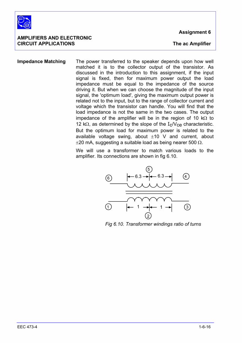
Assignment 6 AMPLIFIERS AND ELECTRONIC CIRCUIT APPLICATIONS The ac Amplifier
EEC 473-4 1-6-16
Impedance Matching The power transferred to the speaker depends upon how well matched it is to the collector output of the transistor. As discussed in the introduction to this assignment, if the input signal is fixed, then for maximum power output the load impedance must be equal to the impedance of the source driving it. But when we can choose the magnitude of the input signal, the 'optimum load', giving the maximum output power is related not to the input, but to the range of collector current and voltage which the transistor can handle. You will find that the load impedance is not the same in the two cases. The output impedance of the amplifier will be in the region of 10 kΩ to 12 kΩ, as determined by the slope of the Ic/Vce characteristic. But the optimum load for maximum power is related to the available voltage swing, about ±10 V and current, about ±20 mA, suggesting a suitable load as being nearer 500 Ω.
We will use a transformer to match various loads to the amplifier. Its connections are shown in fig 6.10.
Fig 6.10. Transformer windings ratio of turns
Assignment 6 AMPLIFIERS AND ELECTRONIC CIRCUIT APPLICATIONS The ac Amplifier
EEC 473-4 1-6-17
Set the output voltage across the loudspeaker to 3 V pk–pk at 1 kHz by adjusting the output of the function generator. Adjust the bias potentiometer for the best sinewave output and reset the output voltage to 3 V if necessary.
Disconnect the leads from the speaker and insert them into the EEC 470 deck in the bottom row extreme right-hand side, four holes apart. Various resistors can then be inserted to represent RL Copy the results table as shown in fig 6.13, reproduced at the end of this assignment. Measure and record the pk–pk value of the output voltage for the values of RL in your table. Use series and parallel combinations to obtain the values needed. These results relate to a turns ratio N of 6.3:1 Complete the table by carrying out the calculations shown in the column headings. For your calculated values of output power, and using the value of RL given, plot a graph of output power against load resistance RL.
Questions 5 What value of RL gives the maximum output power?
6 What is the reflected resistance at maximum output power?
Assignment 6 AMPLIFIERS AND ELECTRONIC CIRCUIT APPLICATIONS The ac Amplifier
EEC 473-4 1-6-18
Matching for Maximum Output Power We will now see whether, given freedom to alter the input
signal, the optimum load changes. Apply as a load to the secondary the same resistance value as gave maximum power in your previous results.
Adjust the input signal to the maximum level possible before distortion becomes noticeable. Calculate the power in the load, as before.
Repeat this test with a 220 Ω load, again adjusting the signal level just to avoid distortion.
Question 7 Does an impedance-matched load give: a best gain? b maximum output?

Ass
ignm
ent 6
A
MPL
IFIE
RS
AN
D E
LEC
TRO
NIC
CIR
CU
IT A
PPLI
CA
TIO
NS
The
ac A
mpl
ifier
E
EC
473
-4
1-6-
19
Not
es
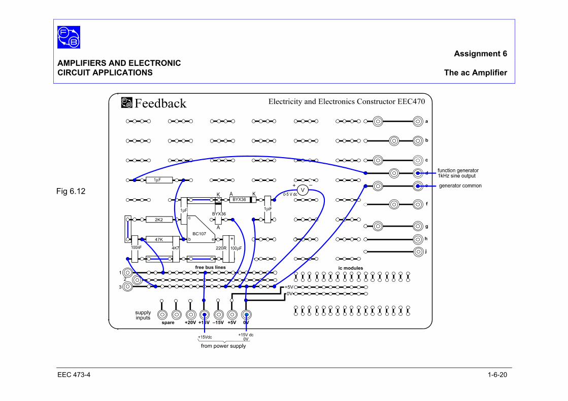
Assignment 6 AMPLIFIERS AND ELECTRONIC CIRCUIT APPLICATIONS The ac Amplifier
EEC 473-4 1-6-20
Fig 6.12
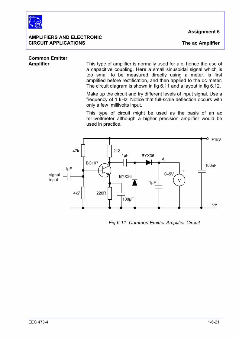
Assignment 6 AMPLIFIERS AND ELECTRONIC CIRCUIT APPLICATIONS The ac Amplifier
EEC 473-4 1-6-21
Common Emitter Amplifier This type of amplifier is normally used for a.c. hence the use of
a capacitive coupling. Here a small sinusoidal signal which is too small to be measured directly using a meter, is first amplified before rectification, and then applied to the dc meter. The circuit diagram is shown in fig 6.11 and a layout in fig 6.12.
Make up the circuit and try different levels of input signal. Use a frequency of 1 kHz. Notice that full-scale deflection occurs with only a few millivolts input.
This type of circuit might be used as the basis of an ac millivoltmeter although a higher precision amplifier would be used in practice.
Fig 6.11 Common Emitter Amplifier Circuit
Assignment 6 AMPLIFIERS AND ELECTRONIC CIRCUIT APPLICATIONS The ac Amplifier
EEC 473-4 1-6-22
PRACTICAL CONSIDERATIONS AND APPLICATIONS In this assignment we have brought together the elements
forming the basic ac common emitter amplifier. The actual values of components that the designer will use will be decided by the characteristics of the transistor, together with the frequency range and output needs.
With a frequency of 1 kHz a 100 µF capacitor acted as a virtual short circuit; if the frequency was 1 MHz then the 1 µF capacitor would have been sufficient.
With a choice of coupling capacitor and resistance values, different values will be needed for operation at different frequency ranges.
Different applications will have different needs for matching. A microphone amplifier, for example, will typically require maximum gain, and is unlikely to be overloaded by excessive output. A loudspeaker amplifier, by contrast, will be provided, by earlier amplifier stages, with as much input as is needed. The requirement will be to produce the largest possible power output. By careful choice of transformer, each of these different needs can be met.
SUMMARY In this assignment you have learnt that: 1 Using an emitter resistor, the bias on the transistor input can
be stabilised against changes in supply voltage. 2 An emitter by-pass capacitor can overcome the loss of gain
with ac signals caused by adding an emitter resistor. 3 Coupling capacitors can remove any inter-stage dc
potentials. 4 A transformer with suitable turns ratio can ensure maximum
power transfer from amplifier output to load.
Assignment 6 AMPLIFIERS AND ELECTRONIC CIRCUIT APPLICATIONS The ac Amplifier
EEC 473-4 1-6-23
EXERCISE With the following symptoms, where would you look if you were repairing a faulty amplifier?
a) With a pure ac signal, the output was correctly biased but the amplification was very low.
b) With an ac signal containing some dc, there was a lot of distortion in the output.
c) The collector has the correct signal but there is distortion in the speaker.

Assignment 6 AMPLIFIERS AND ELECTRONIC CIRCUIT APPLICATIONS The ac Amplifier
EEC 473-4 1-6-24
Notes
Assignment 6 AMPLIFIERS AND ELECTRONIC CIRCUIT APPLICATIONS Answers
EEC 473-4 1-6-25
ANSWERS TO ASSIGNMENT 6 1 The low dc resistance of the function generator has greatly
reduced the dc bias of the amplifier. The transistor is biased off, thus there is no signal output and the collector voltage is equal to the supply voltage. When the input is passed through a capacitor which blocks dc the bias condition is not changed.
2 From the previous assignments we learnt that the voltage
gain is roughly the ratio of the collector resistor to the emitter resistor.
In this case 10100 Ω1k Ω =
3 As the negative feedback to ac is zero the circuit has the
same ac characteristics as the amplifier with no negative feedback.
4 When the capacitor size is reduced the effective emitter
resistance to ac increases, producing negative feedback and reducing the gain.
5 From the graph for N = 6.3:1 the value of RL to give
maximum power output is approximately 45 Ω. 6 The reflected impedance is calculated from the formula :
R'L = N2RL = 6.32 x 45 = 1.8 kΩ
7 An impedance-matched load a. gives the best gain. b. does not necessarily (or usually) give maximum output.
Assignment 6 AMPLIFIERS AND ELECTRONIC CIRCUIT APPLICATIONS Answers
EEC 473-4 1-6-26
Exercise a) If the bias is correct but the gain is low the emitter by-pass capacitor may be open circuit producing ac negative feedback and reducing the gain.
b) This may mean that some of the dc on the input signal is changing the bias conditions of the transistor producing heavy distortion. This could be caused by the input capacitor being short circuit.
c) If the output transformer was shorted some dc could appear on the loudspeaker causing a constant current to flow in the loudspeaker coil producing distortion in it.
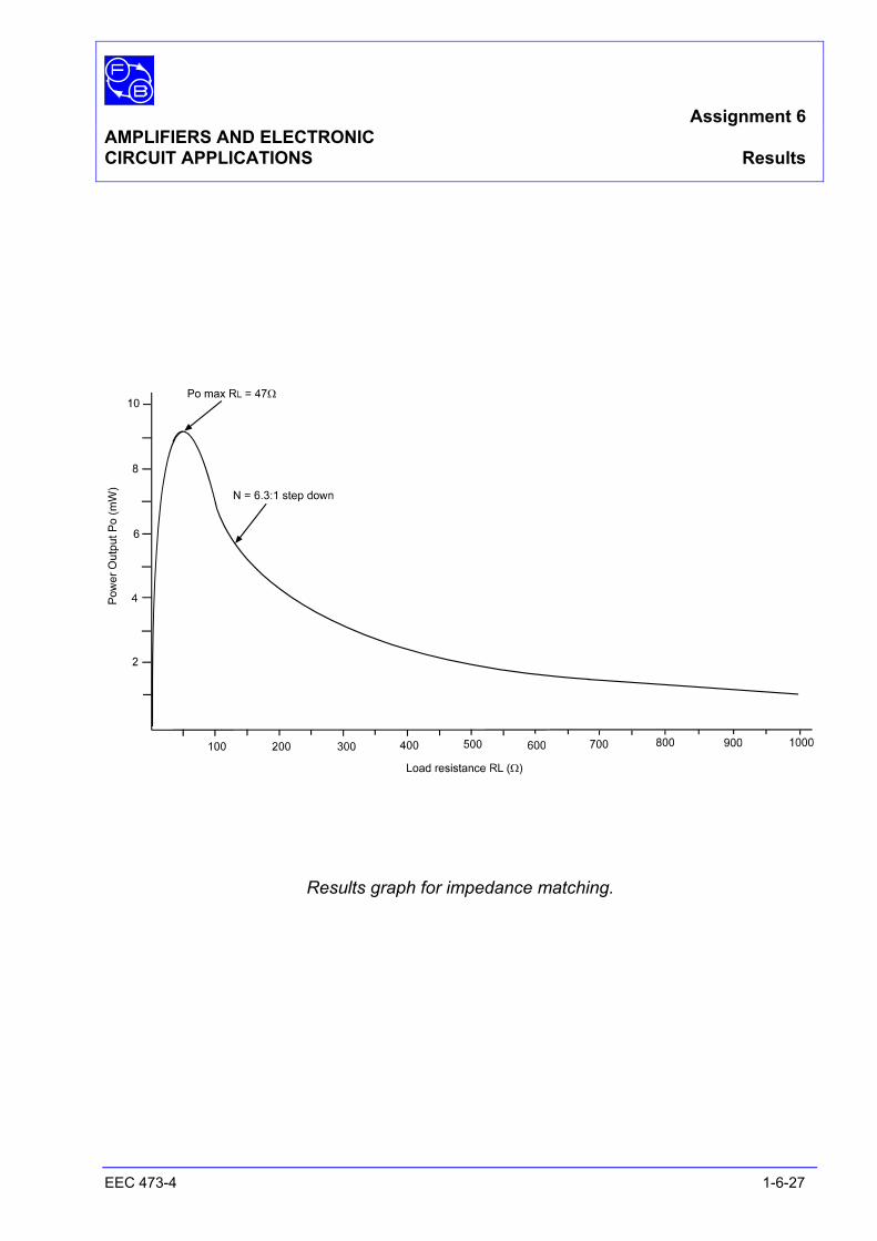
Assignment 6 AMPLIFIERS AND ELECTRONIC CIRCUIT APPLICATIONS Results
EEC 473-4 1-6-27
Results graph for impedance matching.
Assignment 6 AMPLIFIERS AND ELECTRONIC CIRCUIT APPLICATIONS Results
EEC 473-4 1-6-28
Notes
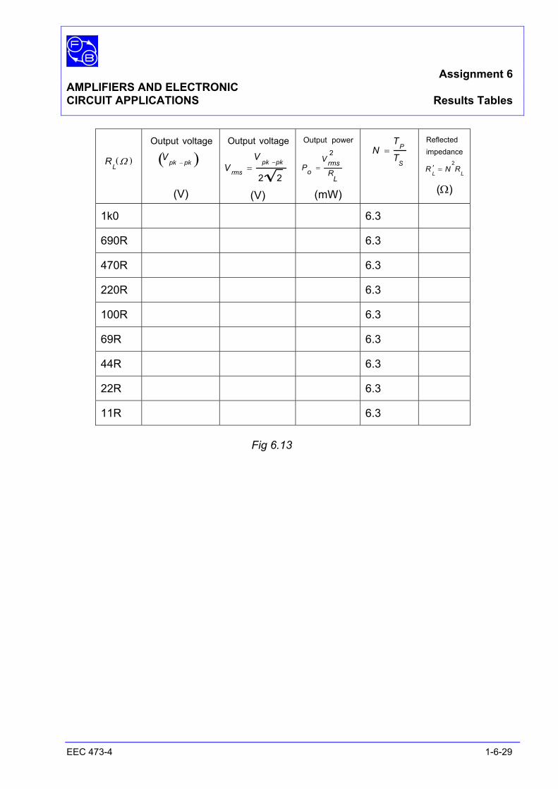
Assignment 6 AMPLIFIERS AND ELECTRONIC CIRCUIT APPLICATIONS Results Tables
EEC 473-4 1-6-29
RLΩ( )
Output voltage
Vpk −pk( )
(V)
Output voltage
V rms =V
pk −pk
2 2
(V)
Output power
Po =V rms
2
RL
(mW)
N =T
P
TS
Reflectedimpedance
R ′L= N
2R
L
(Ω)
1k0 6.3
690R 6.3
470R 6.3
220R 6.3
100R 6.3
69R 6.3
44R 6.3
22R 6.3
11R 6.3
Fig 6.13

Assignment 6 AMPLIFIERS AND ELECTRONIC CIRCUIT APPLICATIONS Results Tables
EEC 473-4 1-6-30
Notes
Assignment 7 AMPLIFIERS AND ELECTRONIC CIRCUIT APPLICATIONS Power Amplifiers
EEC 473-4 1-7-1
OBJECTIVES 1 A knowledge of the function of a power amplifier
2 A knowledge of the design of a power amplifier using push-pull techniques.
EQUIPMENT REQUIRED Qty Apparatus 1 Electricity & Electronics Constructor EEC470 1 Amplifier Kit EEC473-4
1 Power supply unit +15 V dc regulated (eg, Feedback Power Supply 92-445 or optionally the 92-100 Teknikit console) 1 Function generator (eg. Feedback FG601) 1 2–Channel oscilloscope 1 Multimeter or 1 Milliammeter 0-100 mA dc
PREREQUISITE ASSIGNMENTS Assignment 6
KNOWLEDGE LEVEL See prerequisite Assignments
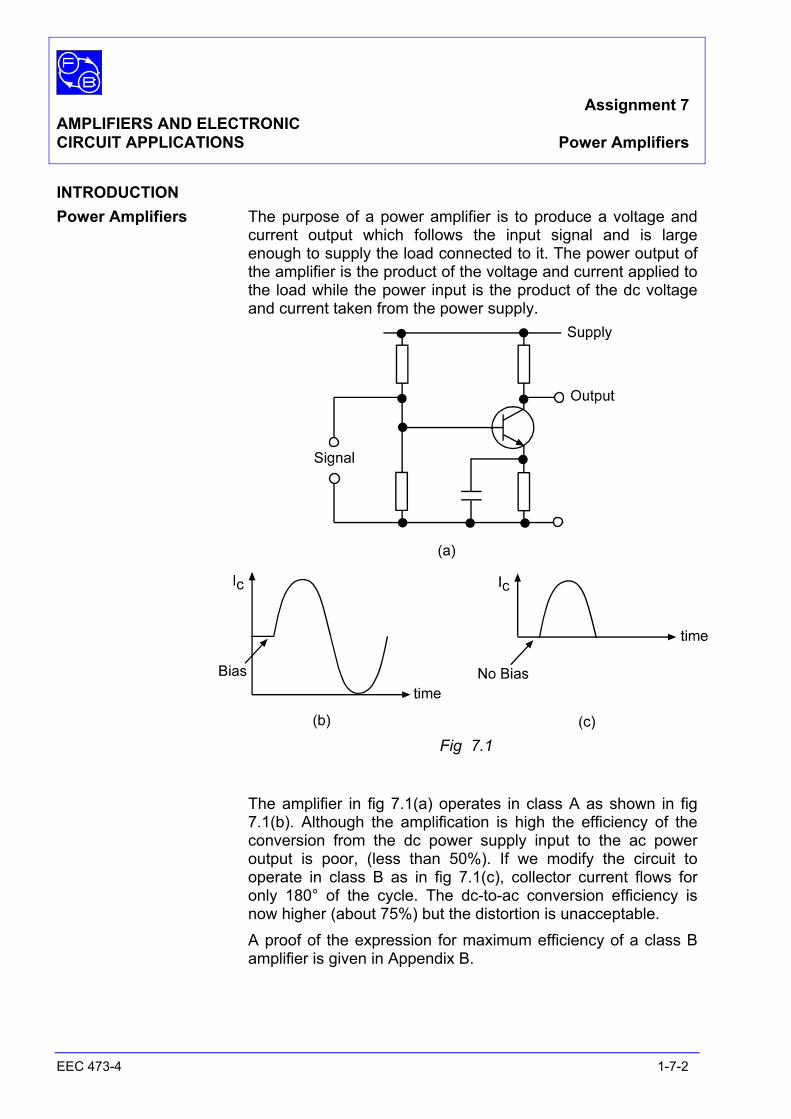
Assignment 7 AMPLIFIERS AND ELECTRONIC CIRCUIT APPLICATIONS Power Amplifiers
EEC 473-4 1-7-2
INTRODUCTION Power Amplifiers The purpose of a power amplifier is to produce a voltage and
current output which follows the input signal and is large enough to supply the load connected to it. The power output of the amplifier is the product of the voltage and current applied to the load while the power input is the product of the dc voltage and current taken from the power supply.
Fig 7.1
The amplifier in fig 7.1(a) operates in class A as shown in fig
7.1(b). Although the amplification is high the efficiency of the conversion from the dc power supply input to the ac power output is poor, (less than 50%). If we modify the circuit to operate in class B as in fig 7.1(c), collector current flows for only 180° of the cycle. The dc-to-ac conversion efficiency is now higher (about 75%) but the distortion is unacceptable.
A proof of the expression for maximum efficiency of a class B amplifier is given in Appendix B.
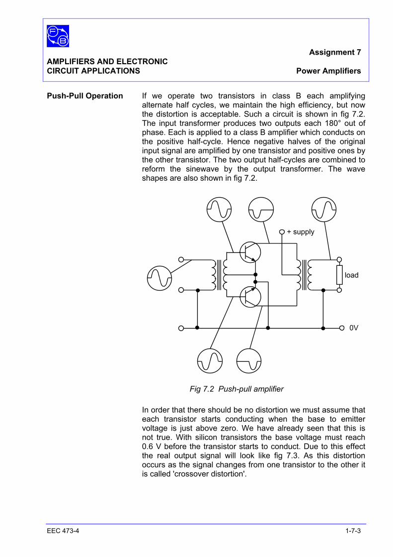
Assignment 7 AMPLIFIERS AND ELECTRONIC CIRCUIT APPLICATIONS Power Amplifiers
EEC 473-4 1-7-3
Push-Pull Operation If we operate two transistors in class B each amplifying alternate half cycles, we maintain the high efficiency, but now the distortion is acceptable. Such a circuit is shown in fig 7.2. The input transformer produces two outputs each 180° out of phase. Each is applied to a class B amplifier which conducts on the positive half-cycle. Hence negative halves of the original input signal are amplified by one transistor and positive ones by the other transistor. The two output half-cycles are combined to reform the sinewave by the output transformer. The wave shapes are also shown in fig 7.2.
Fig 7.2 Push-pull amplifier In order that there should be no distortion we must assume that
each transistor starts conducting when the base to emitter voltage is just above zero. We have already seen that this is not true. With silicon transistors the base voltage must reach 0.6 V before the transistor starts to conduct. Due to this effect the real output signal will look like fig 7.3. As this distortion occurs as the signal changes from one transistor to the other it is called 'crossover distortion'.
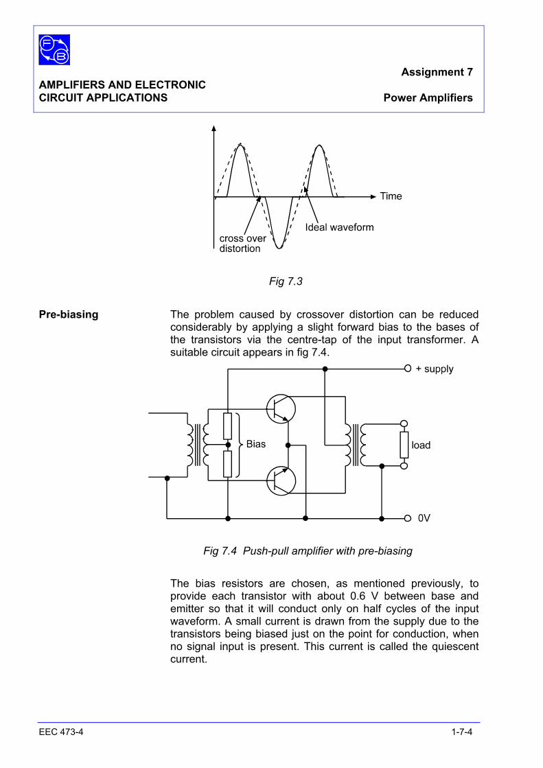
Assignment 7 AMPLIFIERS AND ELECTRONIC CIRCUIT APPLICATIONS Power Amplifiers
EEC 473-4 1-7-4
Fig 7.3 Pre-biasing The problem caused by crossover distortion can be reduced
considerably by applying a slight forward bias to the bases of the transistors via the centre-tap of the input transformer. A suitable circuit appears in fig 7.4.
Fig 7.4 Push-pull amplifier with pre-biasing The bias resistors are chosen, as mentioned previously, to
provide each transistor with about 0.6 V between base and emitter so that it will conduct only on half cycles of the input waveform. A small current is drawn from the supply due to the transistors being biased just on the point for conduction, when no signal input is present. This current is called the quiescent current.
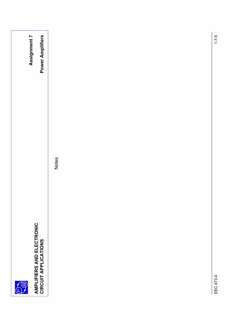
Ass
ignm
ent 7
A
MPL
IFIE
RS
AN
D E
LEC
TRO
NIC
CIR
CU
IT A
PPLI
CA
TIO
NS
Pow
er A
mpl
ifier
s E
EC
473
-4
1-7-
5
Not
es
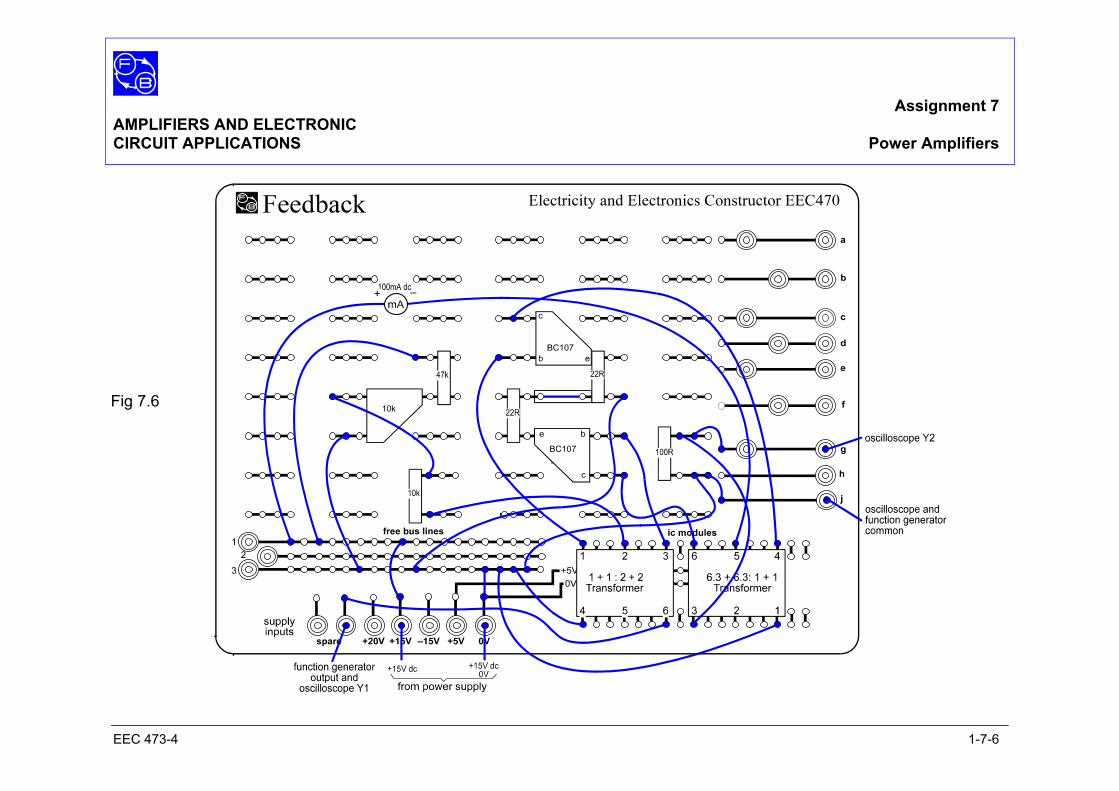
Assignment 7 AMPLIFIERS AND ELECTRONIC CIRCUIT APPLICATIONS Power Amplifiers
EEC 473-4 1-7-6
Fig 7.6
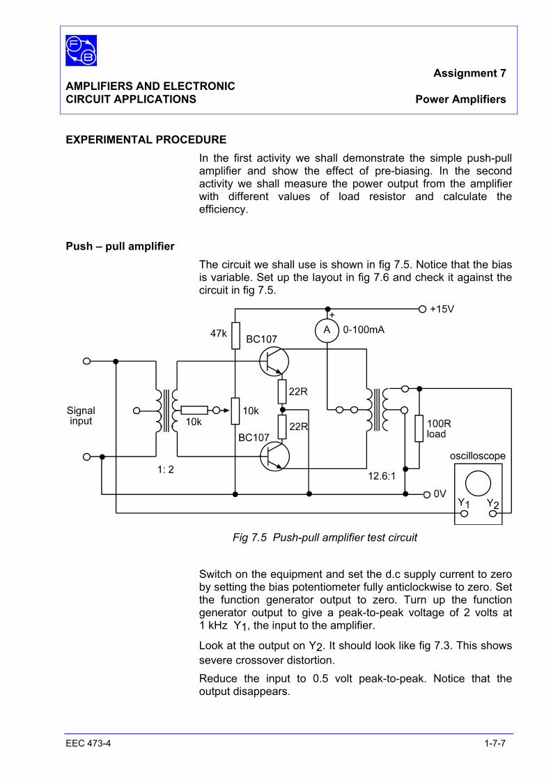
Assignment 7 AMPLIFIERS AND ELECTRONIC CIRCUIT APPLICATIONS Power Amplifiers
EEC 473-4 1-7-7
EXPERIMENTAL PROCEDURE In the first activity we shall demonstrate the simple push-pull
amplifier and show the effect of pre-biasing. In the second activity we shall measure the power output from the amplifier with different values of load resistor and calculate the efficiency.
Push – pull amplifier The circuit we shall use is shown in fig 7.5. Notice that the bias
is variable. Set up the layout in fig 7.6 and check it against the circuit in fig 7.5.
Fig 7.5 Push-pull amplifier test circuit Switch on the equipment and set the d.c supply current to zero
by setting the bias potentiometer fully anticlockwise to zero. Set the function generator output to zero. Turn up the function generator output to give a peak-to-peak voltage of 2 volts at 1 kHz Y1, the input to the amplifier.
Look at the output on Y2. It should look like fig 7.3. This shows severe crossover distortion.
Reduce the input to 0.5 volt peak-to-peak. Notice that the output disappears.
Assignment 7 AMPLIFIERS AND ELECTRONIC CIRCUIT APPLICATIONS Power Amplifiers
EEC 473-4 1-7-8
Question 1 Why does the output disappear when the input level is reduced?
Now set the input to 100 mV peak-to-peak. Slowly apply bias by turning the potentiometer clockwise
observing the oscilloscope trace Y2 as you do so, but do not exceed 10 mA on the meter.
Notice that the crossover distortion is eliminated when the supply current, indicated on the meter, reaches about 0.6 mA.
Vary the bias current from zero to 10 mA and observe the change in crossover distortion. The change in supply current from 3—10 mA makes little improvement on the already near perfect waveform, but what value of current is required for normal operation?
With the output of the function generator set to zero adjust the bias for a quiescent current of 20mA. Vary the input from the function generator from zero to 0.1 V peak-to-peak and observe the output waveform and the current.
You will notice little change in the current taken from the supply. That is because the amplifier is operating in the class A mode.
Now set the function generator for 0.1 V peak-to-peak output and adjust the bias potentiometer to eliminate crossover distortion. Finely adjust the bias until the point where the waveform passes through zero is straight and continuous as shown in the ideal waveform fig 7.3. When you are satisfied with the adjustment reduce the input from the function generator to zero and observe the quiescent current on the meter. It should be about 0.5 mA.
Now vary the input from the function generator from zero to 1V peak-to-peak and watch the supply current change from the quiescent value up to about 5 mA. The amplifier is now biased for class B operation. The low supply current with no input signal being one of the main advantages over the class A amplifier.
Power amplifier We shall use the same test circuit as for the first activity.
Copy the results table as shown in fig 7.9, reproduced at the end of this assignment.
Now set the function generator so that the OUTPUT of the amplifier is 4 V peak-to-peak and adjust the bias potentiometer to eliminate crossover distortion.
Assignment 7 AMPLIFIERS AND ELECTRONIC CIRCUIT APPLICATIONS Power Amplifiers
EEC 473-4 1-7-9
Measure the output peak-to-peak voltage and record it in the table. Change the load resistor for the other values in the table, entering the output voltage each time. Use series and parallel resistor combinations as necessary. Do not change the input amplitude and bias setting.
Convert each output voltage reading to its root mean square equivalent by using the formula:
Vrms = 22
peaktopeakV −−
(A proof of this appears in Appendix C) From this, the output power can be calculated. Using the formula
Power = ( )loadR
2rmsV
Enter the power output in the results table.
Questions 2 Which value of load resistor gives maximum power? 3 What does this imply about the output impedance
of the amplifier ? Select the resistor that matches the output impedance most
closely, and replace the load resistor with it. Turn up the function generator output for maximum undistorted
output on Y2. Notice that the supply current increases when an input is applied to the amplifier and it draws only a small current when it is supplying no output power.
Measure the output power of the amplifier as before by measuring the peak-to-peak output voltage. Measure the supply current and using the formula:
Pin = Vsupply x Isupply
= 15 x Isupply

Assignment 7 AMPLIFIERS AND ELECTRONIC CIRCUIT APPLICATIONS Power Amplifiers
EEC 473-4 1-7-10
Calculate the input power to the amplifier. Now we can calculate the efficiency of the amplifier. Use the
formula:
Efficiency = inP
outP x 100%
Question 4 What is the efficiency of the amplifier?

Ass
ignm
ent 7
A
MPL
IFIE
RS
AN
D E
LEC
TRO
NIC
CIR
CU
IT A
PPLI
CA
TIO
NS
Pow
er A
mpl
ifier
s E
EC
473
-4
1-7-
11
Not
es
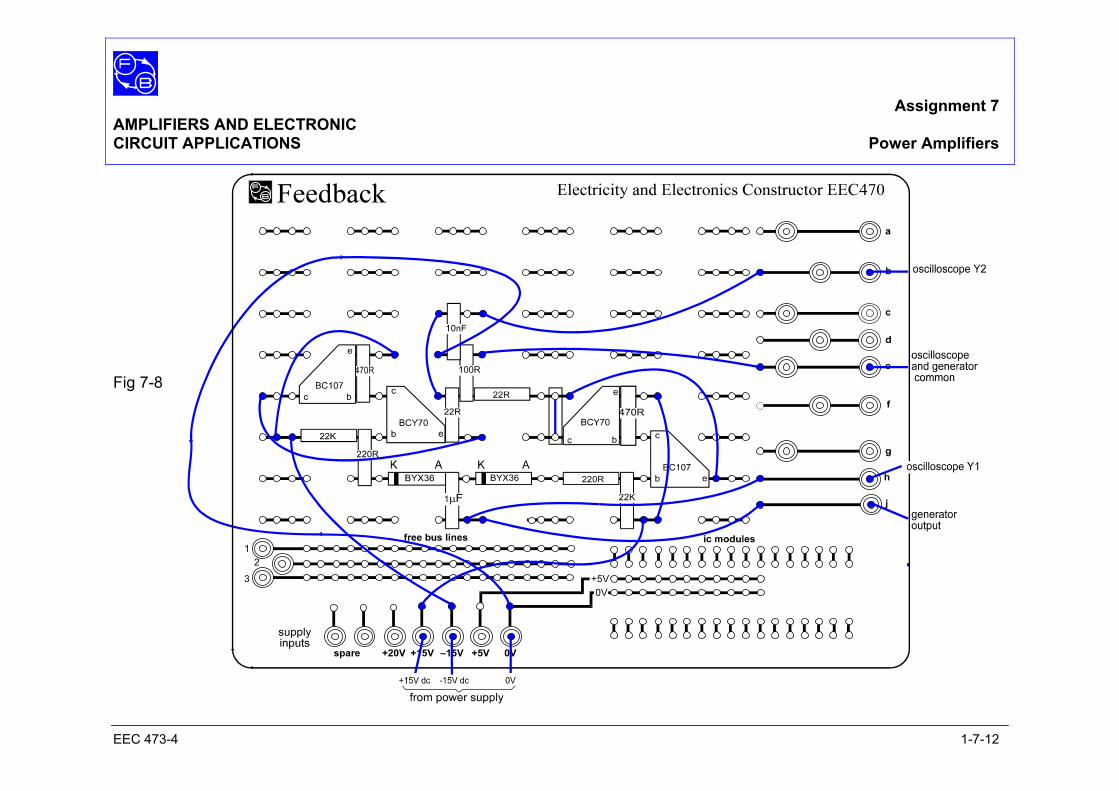
Assignment 7 AMPLIFIERS AND ELECTRONIC CIRCUIT APPLICATIONS Power Amplifiers
EEC 473-4 1-7-12
Fig 7-8
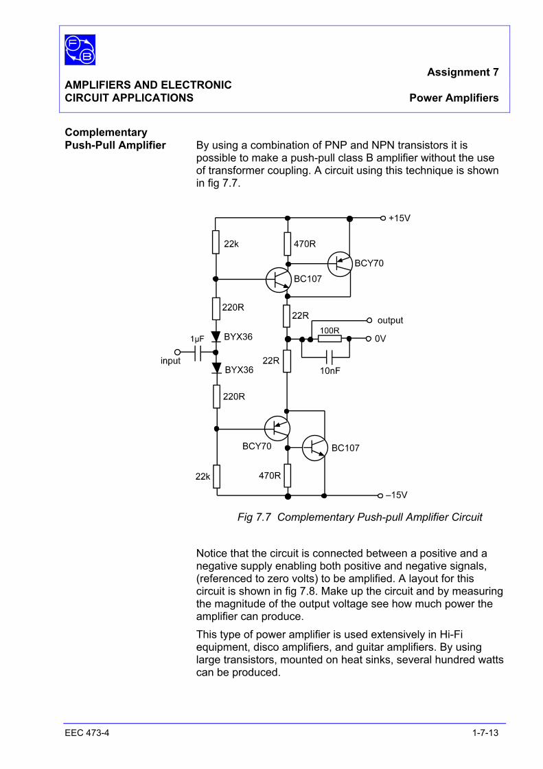
Assignment 7 AMPLIFIERS AND ELECTRONIC CIRCUIT APPLICATIONS Power Amplifiers
EEC 473-4 1-7-13
Complementary Push-Pull Amplifier By using a combination of PNP and NPN transistors it is
possible to make a push-pull class B amplifier without the use of transformer coupling. A circuit using this technique is shown in fig 7.7.
Fig 7.7 Complementary Push-pull Amplifier Circuit
Notice that the circuit is connected between a positive and a
negative supply enabling both positive and negative signals, (referenced to zero volts) to be amplified. A layout for this circuit is shown in fig 7.8. Make up the circuit and by measuring the magnitude of the output voltage see how much power the amplifier can produce.
This type of power amplifier is used extensively in Hi-Fi equipment, disco amplifiers, and guitar amplifiers. By using large transistors, mounted on heat sinks, several hundred watts can be produced.
Assignment 7 AMPLIFIERS AND ELECTRONIC CIRCUIT APPLICATIONS Power Amplifiers
EEC 473-4 1-7-14
PRACTICAL CONSIDERATIONS AND APPLICATION As we can see from the practical activities the practical
efficiency is low compared with the theoretical value. This is mainly due to circuit losses. The most 'lossy' components are the transformers and, using modern circuit techniques, excellent class B push-pull amplifiers can be built using complementary transistors to replace the transformers. This also improves the frequency response greatly.
Even harmonics will also cancel due to their opposite phase relationship. This has the effect of reducing the distortion for a given power output.
Most high power audio amplifiers use the push-pull configuration and by using additional components very high output powers with very low distortion can be obtained.
SUMMARY In this assignment you have learnt that: 1 Class B amplifiers are more efficient than Class A
amplifiers but produce high distortion. 2 By using the push-pull configuration the distortion can be
reduced. 3 Simple push-pull amplifiers produce high crossover
distortion. 4 Pre-biasing will prevent crossover distortion.
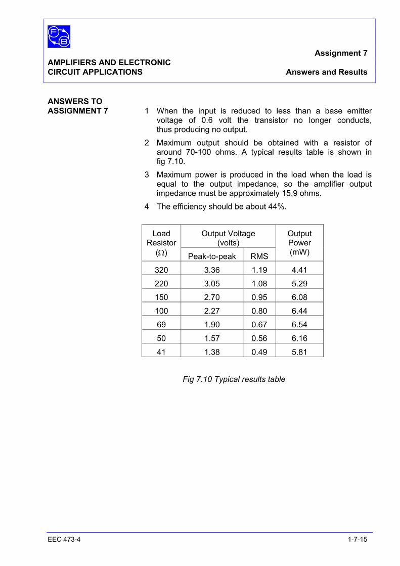
Assignment 7 AMPLIFIERS AND ELECTRONIC CIRCUIT APPLICATIONS Answers and Results
EEC 473-4 1-7-15
ANSWERS TO ASSIGNMENT 7 1 When the input is reduced to less than a base emitter
voltage of 0.6 volt the transistor no longer conducts, thus producing no output.
2 Maximum output should be obtained with a resistor of around 70-100 ohms. A typical results table is shown in fig 7.10.
3 Maximum power is produced in the load when the load is equal to the output impedance, so the amplifier output impedance must be approximately 15.9 ohms. 4 The efficiency should be about 44%.
Output Voltage (volts)
Load Resistor
(Ω) Peak-to-peak RMS
Output Power (mW)
320 3.36 1.19 4.41
220 3.05 1.08 5.29
150 2.70 0.95 6.08
100 2.27 0.80 6.44
69 1.90 0.67 6.54
50 1.57 0.56 6.16
41 1.38 0.49 5.81
Fig 7.10 Typical results table

Assignment 7 AMPLIFIERS AND ELECTRONIC CIRCUIT APPLICATIONS Answers and Results
EEC 473-4 1-7-16
Notes
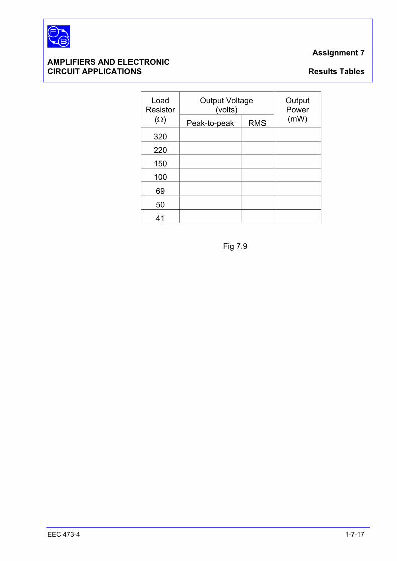
Assignment 7 AMPLIFIERS AND ELECTRONIC CIRCUIT APPLICATIONS Results Tables
EEC 473-4 1-7-17
Output Voltage (volts)
Load Resistor
(Ω) Peak-to-peak RMS
Output Power (mW)
320
220
150
100
69
50
41
Fig 7.9
Assignment 7 AMPLIFIERS AND ELECTRONIC CIRCUIT APPLICATIONS Results Tables
EEC 473-4 1-7-18
Notes
Assignment 8 AMPLIFIERS AND ELECTRONIC CIRCUIT APPLICATIONS Passive Attenuators
EEC 473-4 1-8-1
OBJECTIVE To understand the use of passive attenuators.
EQUIPMENT REQUIRED Qty Apparatus 1 Electricity & Electronics Constructor
EEC470 1 Amplifier Kit EEC473-4 1 Power supply unit +15 V dc. regulated
(eg, Feedback Power Supply 92-445 or optionally the 92-100 Teknikit console)
1 Function generator. Sinusoidal 10 V pk-to- pk @ 1 kHz (eg. Feedback FG601)
1 Oscilloscope 1 Multimeter or
1 Ohmmeter 0-30 kΩ
PREREQUISITE ASSIGNMENTS Assignment 4
KNOWLEDGE LEVEL See prerequisite assignments

Assignment 8 AMPLIFIERS AND ELECTRONIC CIRCUIT APPLICATIONS Passive Attenuators
EEC 473-4 1-8-2
Notes
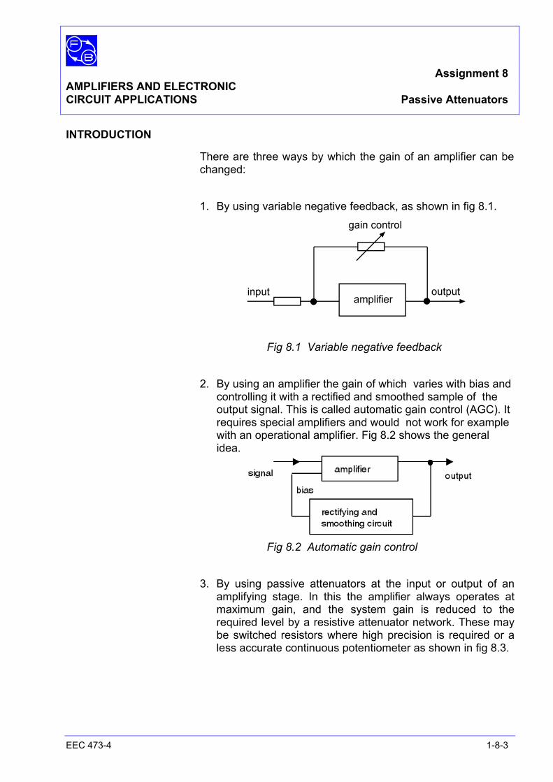
Assignment 8 AMPLIFIERS AND ELECTRONIC CIRCUIT APPLICATIONS Passive Attenuators
EEC 473-4 1-8-3
INTRODUCTION
There are three ways by which the gain of an amplifier can be changed:
1. By using variable negative feedback, as shown in fig 8.1.
Fig 8.1 Variable negative feedback 2. By using an amplifier the gain of which varies with bias and
controlling it with a rectified and smoothed sample of the output signal. This is called automatic gain control (AGC). It requires special amplifiers and would not work for example with an operational amplifier. Fig 8.2 shows the general idea.
Fig 8.2 Automatic gain control 3. By using passive attenuators at the input or output of an
amplifying stage. In this the amplifier always operates at maximum gain, and the system gain is reduced to the required level by a resistive attenuator network. These may be switched resistors where high precision is required or a less accurate continuous potentiometer as shown in fig 8.3.
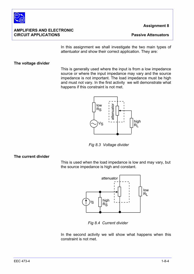
Assignment 8 AMPLIFIERS AND ELECTRONIC CIRCUIT APPLICATIONS Passive Attenuators
EEC 473-4 1-8-4
In this assignment we shall investigate the two main types of attentuator and show their correct application. They are:
The voltage divider This is generally used where the input is from a low impedance
source or where the input impedance may vary and the source impedance is not important. The load impedance must be high and must not vary. In the first activity we will demonstrate what happens if this constraint is not met.
Fig 8.3 Voltage divider The current divider This is used when the load impedance is low and may vary, but
the source impedance is high and constant.
Fig 8.4 Current divider In the second activity we will show what happens when this
constraint is not met.

Ass
ignm
ent 8
A
MPL
IFIE
RS
AN
D E
LEC
TRO
NIC
CIR
CU
IT A
PPLI
CA
TIO
NS
Pass
ive
Atte
nuat
ors
EE
C 4
73-4
1-
8-5
Not
es
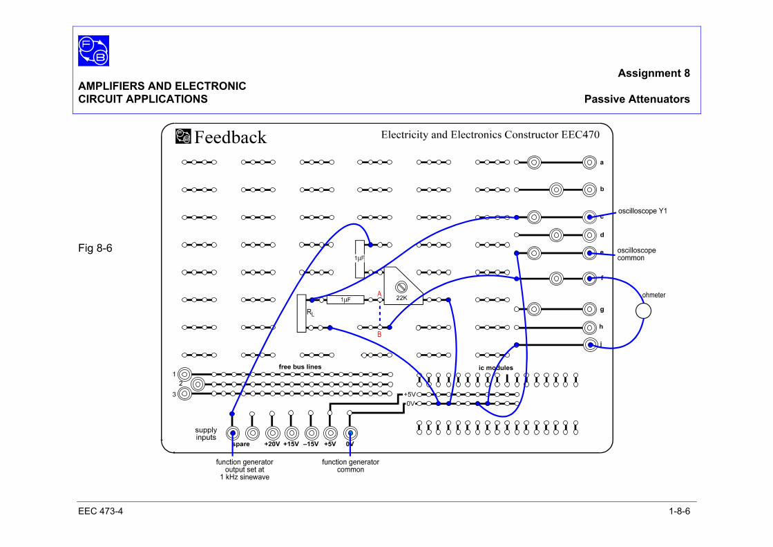
Assignment 8 AMPLIFIERS AND ELECTRONIC CIRCUIT APPLICATIONS Passive Attenuators
EEC 473-4 1-8-6
Fig 8-6
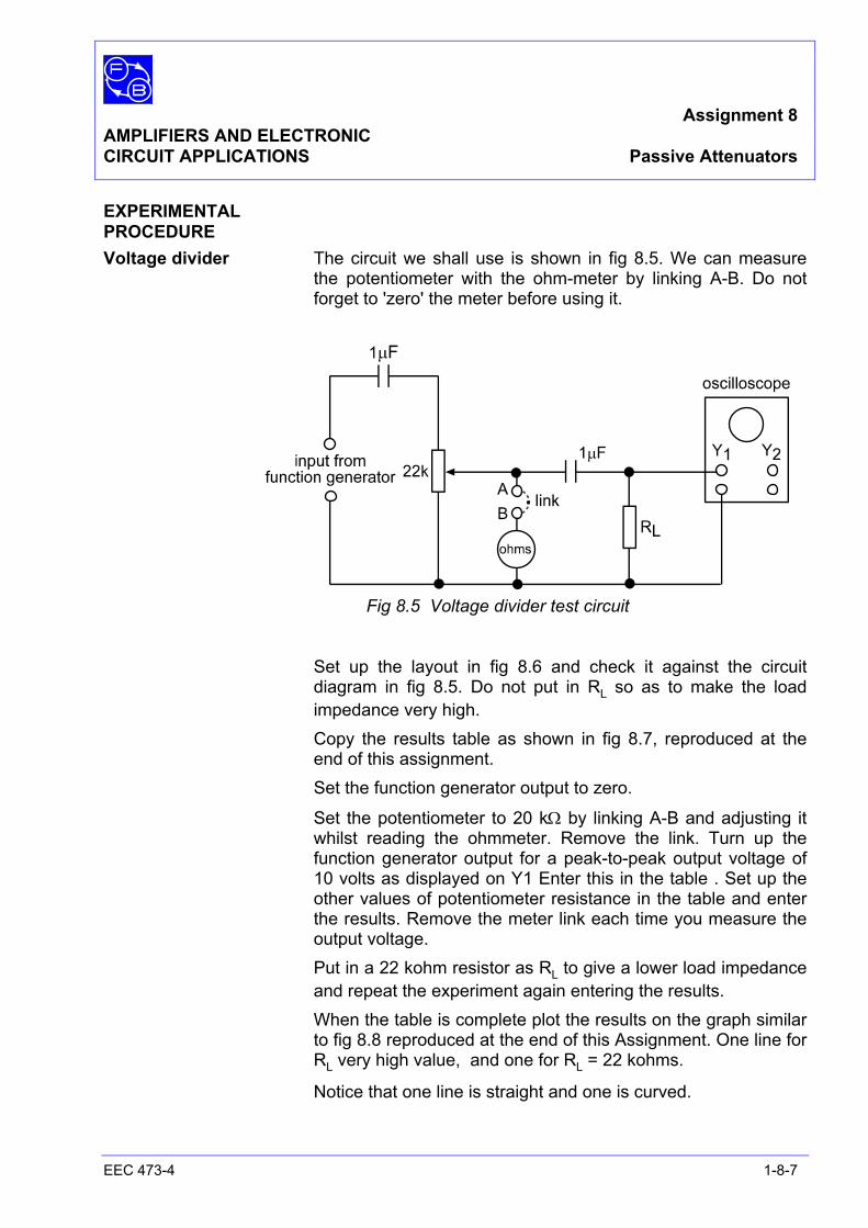
Assignment 8 AMPLIFIERS AND ELECTRONIC CIRCUIT APPLICATIONS Passive Attenuators
EEC 473-4 1-8-7
EXPERIMENTAL PROCEDURE Voltage divider The circuit we shall use is shown in fig 8.5. We can measure
the potentiometer with the ohm-meter by linking A-B. Do not forget to 'zero' the meter before using it.
Fig 8.5 Voltage divider test circuit
Set up the layout in fig 8.6 and check it against the circuit diagram in fig 8.5. Do not put in RL so as to make the load impedance very high.
Copy the results table as shown in fig 8.7, reproduced at the end of this assignment.
Set the function generator output to zero.
Set the potentiometer to 20 kΩ by linking A-B and adjusting it whilst reading the ohmmeter. Remove the link. Turn up the function generator output for a peak-to-peak output voltage of 10 volts as displayed on Y1 Enter this in the table . Set up the other values of potentiometer resistance in the table and enter the results. Remove the meter link each time you measure the output voltage.
Put in a 22 kohm resistor as RL to give a lower load impedance and repeat the experiment again entering the results.
When the table is complete plot the results on the graph similar to fig 8.8 reproduced at the end of this Assignment. One line for RL very high value, and one for RL = 22 kohms.
Notice that one line is straight and one is curved.
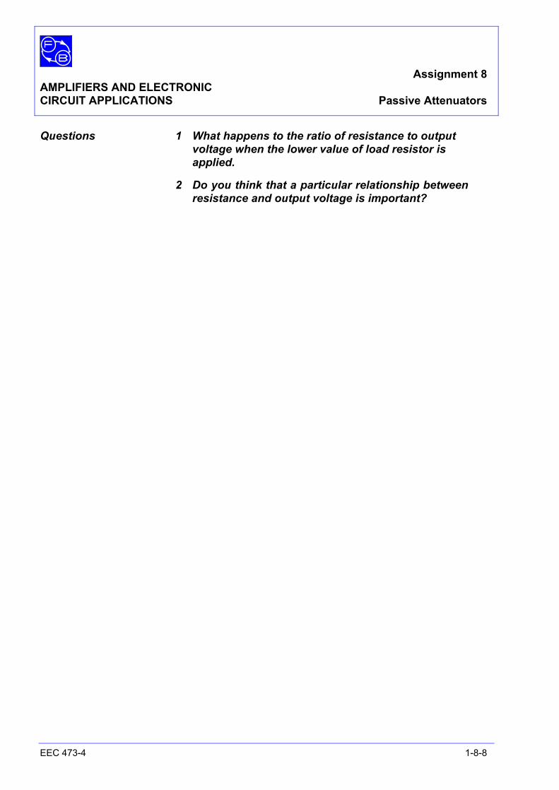
Assignment 8 AMPLIFIERS AND ELECTRONIC CIRCUIT APPLICATIONS Passive Attenuators
EEC 473-4 1-8-8
Questions 1 What happens to the ratio of resistance to output voltage when the lower value of load resistor is applied.
2 Do you think that a particular relationship between resistance and output voltage is important?
Ass
ignm
ent 8
A
MPL
IFIE
RS
AN
D E
LEC
TRO
NIC
CIR
CU
IT A
PPLI
CA
TIO
NS
Pass
ive
Atte
nuat
ors
EE
C 4
73-4
1-
8-9
Not
es
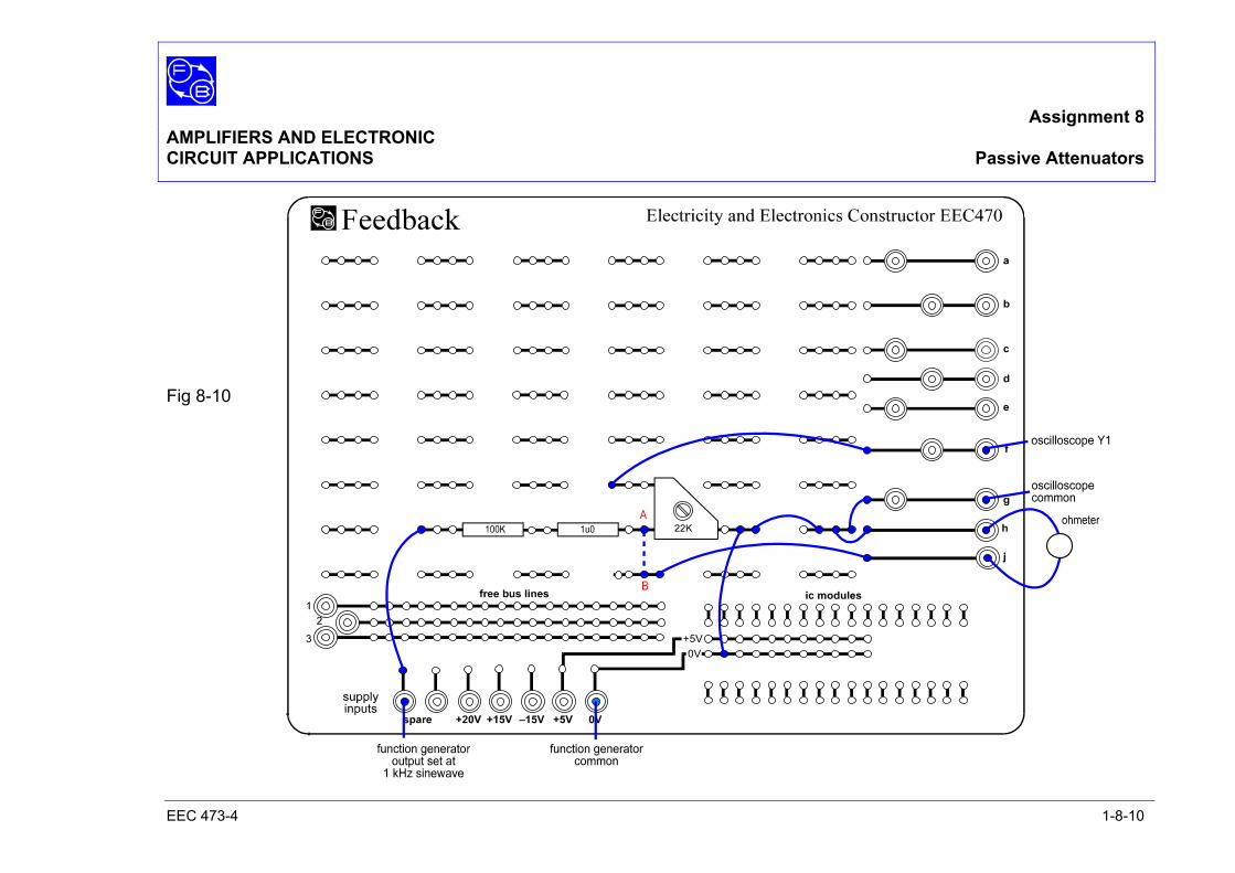
Assignment 8 AMPLIFIERS AND ELECTRONIC CIRCUIT APPLICATIONS Passive Attenuators
EEC 473-4 1-8-10
Fig 8-10
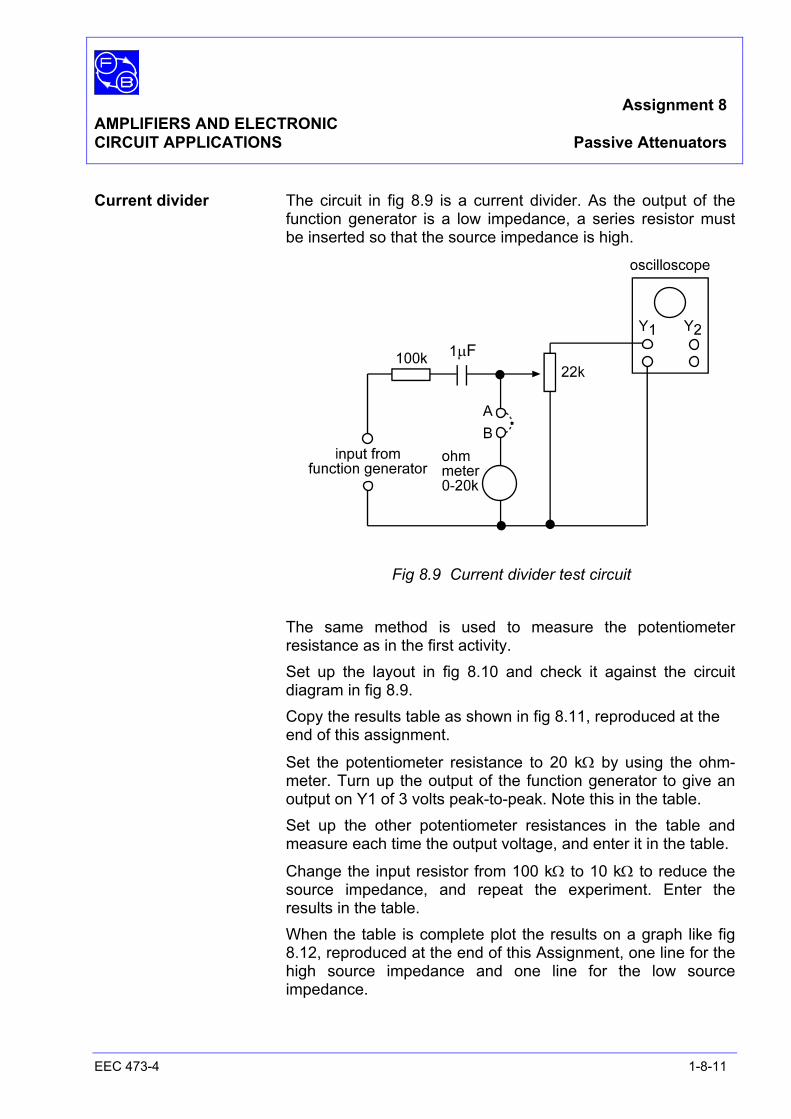
Assignment 8 AMPLIFIERS AND ELECTRONIC CIRCUIT APPLICATIONS Passive Attenuators
EEC 473-4 1-8-11
Current divider The circuit in fig 8.9 is a current divider. As the output of the function generator is a low impedance, a series resistor must be inserted so that the source impedance is high.
Fig 8.9 Current divider test circuit The same method is used to measure the potentiometer
resistance as in the first activity. Set up the layout in fig 8.10 and check it against the circuit
diagram in fig 8.9. Copy the results table as shown in fig 8.11, reproduced at the end of this assignment.
Set the potentiometer resistance to 20 kΩ by using the ohm-meter. Turn up the output of the function generator to give an output on Y1 of 3 volts peak-to-peak. Note this in the table.
Set up the other potentiometer resistances in the table and measure each time the output voltage, and enter it in the table.
Change the input resistor from 100 kΩ to 10 kΩ to reduce the source impedance, and repeat the experiment. Enter the results in the table.
When the table is complete plot the results on a graph like fig 8.12, reproduced at the end of this Assignment, one line for the high source impedance and one line for the low source impedance.
Assignment 8 AMPLIFIERS AND ELECTRONIC CIRCUIT APPLICATIONS Passive Attenuators
EEC 473-4 1-8-12
Notice that when using a current divider the source impedance affects the shape of the graph while when using the voltage divider the load impedance affects the graph shape.
Assignment 8 AMPLIFIERS AND ELECTRONIC CIRCUIT APPLICATIONS Passive Attenuators
EEC 473-4 1-8-13
PRACTICAL CONSIDERATIONS AND APPLICATIONS As we have seen, different applications require the use of
different types of attenuator. The most common application of the potentiometer attenuator is the 'volume control' in audio amplifiers. In this arrangement the amplifier operates at maximum gain and the attenuator is placed at the input. This has the disadvantage that the amplifier noise is also subject to this maximum amplification.
SUMMARY In this assignment you have learnt that: 1. Attenuators can be used to reduce the gain of an amplifier. 2. Simple passive or resistive attenuators can be formed from
potentiometers and come in two types, voltage dividers and current dividers.
3. Attenuators can produce an output proportional to the position of a potentiometer slider within certain constraints of source and load impedance.

Assignment 8 AMPLIFIERS AND ELECTRONIC CIRCUIT APPLICATIONS Passive Attenuators
EEC 473-4 1-8-14
Notes
Assignment 8 AMPLIFIERS AND ELECTRONIC CIRCUIT APPLICATIONS Answers and Results
EEC 473-4 1-8-15
ANSWERS TO ASSIGNMENT 8 1 When the load impedance is low the graph becomes
curved showing that the relationship between the slider position and the output voltage is not linear.
2 A linear relationship is important for the ease of control and imperative if the control is calibrated.
Typical results tables are given for the voltage divider circuit in
fig 8.13 and for the current divider circuit in fig 8.14; typical graphs appear in fig 8.15 and fig 8.16 respectively.
Resistance Peak-to-peak output voltage
RL very high RL=22 kΩ
22 kΩ 10 V 10.0
15 kΩ 7.5 V 6.0
10 kΩ 5.0 V 3.9
5 kΩ 2.5 V 2.0
2 kΩ 1.0 V 0.39
0 0.0 0.0
Fig 8.13
Assignment 8 AMPLIFIERS AND ELECTRONIC CIRCUIT APPLICATIONS Answers and Results
EEC 473-4 1-8-16
Fig 8.15
Resistance Peak-to-peak output voltage
High source Low source Z
22 kΩ 3.0 V 3.0 V
15 kΩ 2.25 V 2.7 V
10 kΩ 1.50 V 2.2 V
5 kΩ 0.75 V 1.6 V
2 kΩ 0.30 V 0.45 V
0 0.0 V 0.0 V
Fig 8.14
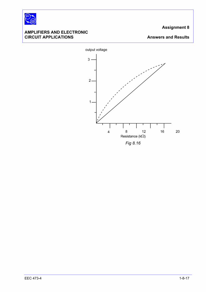
Assignment 8 AMPLIFIERS AND ELECTRONIC CIRCUIT APPLICATIONS Answers and Results
EEC 473-4 1-8-17
Fig 8.16

Assignment 8 AMPLIFIERS AND ELECTRONIC CIRCUIT APPLICATIONS Answers and Results
EEC 473-4 1-8-18
Notes
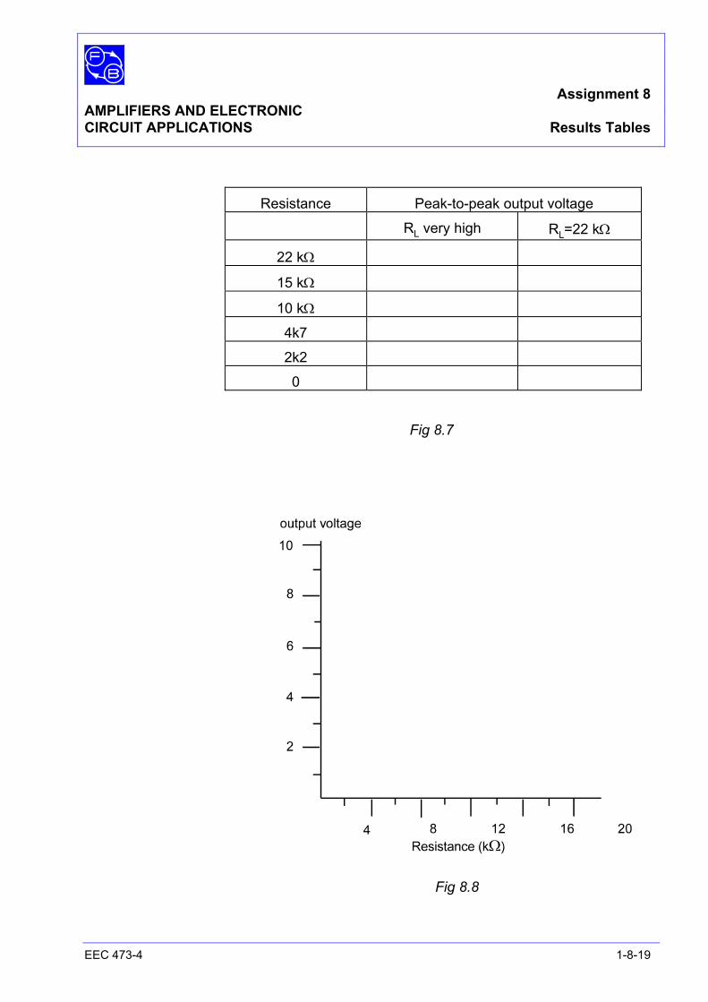
Assignment 8 AMPLIFIERS AND ELECTRONIC CIRCUIT APPLICATIONS Results Tables
EEC 473-4 1-8-19
Resistance Peak-to-peak output voltage
RL very high RL=22 kΩ
22 kΩ
15 kΩ
10 kΩ
4k7
2k2
0
Fig 8.7
Fig 8.8
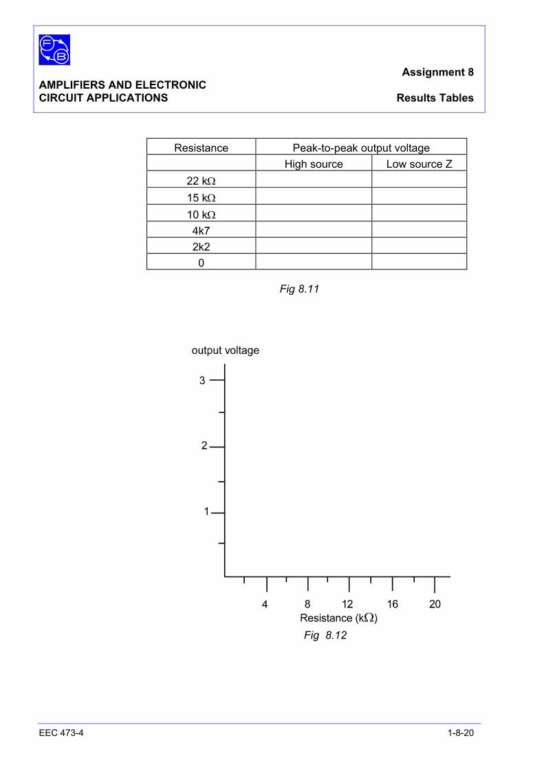
Assignment 8 AMPLIFIERS AND ELECTRONIC CIRCUIT APPLICATIONS Results Tables
EEC 473-4 1-8-20
Resistance Peak-to-peak output voltage
High source Low source Z 22 kΩ 15 kΩ 10 kΩ 4k7 2k2 0
Fig 8.11
Fig 8.12
Assignment 9 AMPLIFIERS AND ELECTRONICS CIRCUIT APPLICATIONS The Operational Amplifier
EEC 473-4 1-9-1
OBJECTIVES. 1. A knowledge of differential amplifiers 2. A knowledge of differential input and high gain
of operational amplifiers.
EQUIPMENT REQUIRED Qty Apparatus 1 Electricity & Electronics Constructor EEC470 1 Amplifier Kit EEC473-4 1 Power supply unit 0 to +20 V variable dc and ±15 V dc regulated (eg, Feedback Power Supply 92-445 or 92-100 Teknikit Console) 1 Function generator sinewave 1 V at 1 kHz (eg, Feedback FG601) 2 Multimeters or 2 Voltmeters 15 V dc 1 2-Channel oscilloscope
PREREQUISITE ASSIGNMENTS Assignment 6
KNOWLEDGE LEVEL Before working this assignment you should :
• Know the operation of ac coupled amplifier circuits with and without negative feedback applied.
Assignment 9 AMPLIFIERS AND ELECTRONICS CIRCUIT APPLICATIONS The Operational Amplifier
EEC 473-4 1-9-2
Notes
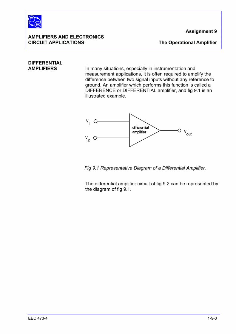
Assignment 9 AMPLIFIERS AND ELECTRONICS CIRCUIT APPLICATIONS The Operational Amplifier
EEC 473-4 1-9-3
DIFFERENTIAL AMPLIFIERS In many situations, especially in instrumentation and
measurement applications, it is often required to amplify the difference between two signal inputs without any reference to ground. An amplifier which performs this function is called a DIFFERENCE or DIFFERENTIAL amplifier, and fig 9.1 is an illustrated example.
Fig 9.1 Representative Diagram of a Differential Amplifier. The differential amplifier circuit of fig 9.2.can be represented by
the diagram of fig 9.1.

Assignment 9 AMPLIFIERS AND ELECTRONICS CIRCUIT APPLICATIONS The Operational Amplifier
EEC 473-4 1-9-4
Notes

Ass
ignm
ent 9
A
MPL
IFIE
RS
AN
D E
LEC
TRO
NIC
S
CIR
CU
IT A
PPLI
CA
TIO
NS
The
Ope
ratio
nal A
mpl
ifier
E
EC
473
-4
1-9-
5
Not
es
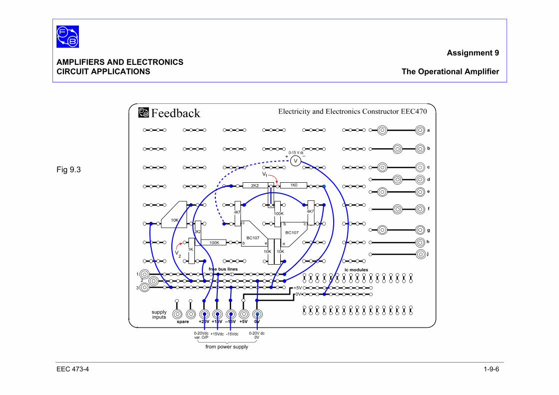
Assignment 9 AMPLIFIERS AND ELECTRONICS CIRCUIT APPLICATIONS The Operational Amplifier
EEC 473-4 1-9-6
Fig 9.3
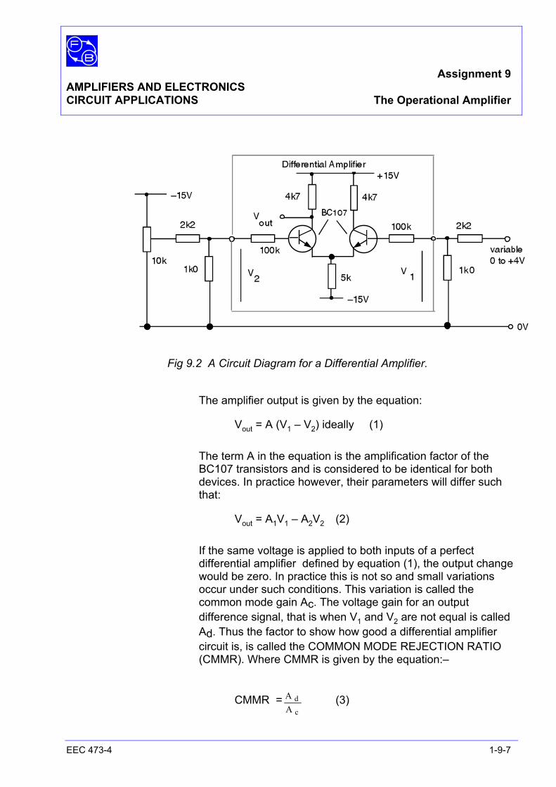
Assignment 9 AMPLIFIERS AND ELECTRONICS CIRCUIT APPLICATIONS The Operational Amplifier
EEC 473-4 1-9-7
Fig 9.2 A Circuit Diagram for a Differential Amplifier. The amplifier output is given by the equation:
Vout = A (V1 – V2) ideally (1)
The term A in the equation is the amplification factor of the BC107 transistors and is considered to be identical for both devices. In practice however, their parameters will differ such that:
Vout = A1V1 – A2V2 (2)
If the same voltage is applied to both inputs of a perfect differential amplifier defined by equation (1), the output change would be zero. In practice this is not so and small variations occur under such conditions. This variation is called the common mode gain Ac. The voltage gain for an output difference signal, that is when V1 and V2 are not equal is called Ad. Thus the factor to show how good a differential amplifier circuit is, is called the COMMON MODE REJECTION RATIO (CMMR). Where CMMR is given by the equation:–
CMMR = AA
d
c (3)
Assignment 9 AMPLIFIERS AND ELECTRONICS CIRCUIT APPLICATIONS The Operational Amplifier
EEC 473-4 1-9-8
The voltage gain can be measured directly by setting V1 = 0.5 V and V2 =–0.5 V Under these conditions, the output voltage Vout gives the gain Ad for the difference signal. Similarly, if V1 = V2 = 1 V, then the change in Vout will equal Ac and the common mode rejection ratio CMMR, can be calculated.
The circuit diagram of fig 9.2 is represented by the layout diagram fig 9.3. The meter is connected to measure Vout and this should be done initially with the 2k2 resistors disconnected.
Replace the resistors and using the meter, apply, via the 10 k potentiometer, a V2 of –0.5 V, and a V1 of +0.5 V from the variable dc. input. Measure Vout and find the difference from the initial reading. This will give you Ad.
To obtain Ac, change the 10 k potentiometer lead from the –15 V terminal to the +15 V terminal and set V2 to +1 V. Set V1 to +1 V and measure Vout. Find the difference from the initial value and calculate the common mode rejection ratio CMMR. A typical value for CMMR is about 15 indicating that the circuit is not a terribly good differential amplifier.
In more advanced circuits (employing constant current sources) CMMR can be several hundreds.
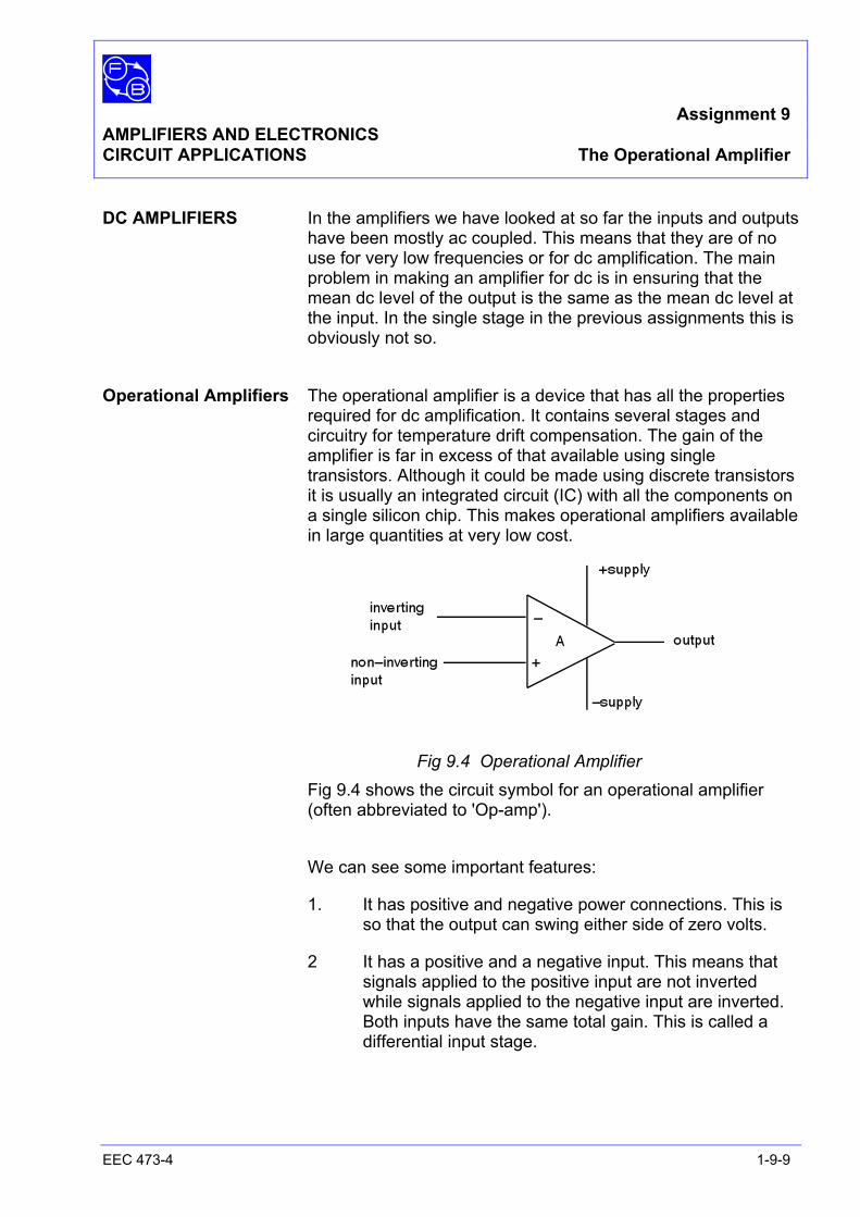
Assignment 9 AMPLIFIERS AND ELECTRONICS CIRCUIT APPLICATIONS The Operational Amplifier
EEC 473-4 1-9-9
DC AMPLIFIERS In the amplifiers we have looked at so far the inputs and outputs have been mostly ac coupled. This means that they are of no use for very low frequencies or for dc amplification. The main problem in making an amplifier for dc is in ensuring that the mean dc level of the output is the same as the mean dc level at the input. In the single stage in the previous assignments this is obviously not so.
Operational Amplifiers The operational amplifier is a device that has all the properties required for dc amplification. It contains several stages and circuitry for temperature drift compensation. The gain of the amplifier is far in excess of that available using single transistors. Although it could be made using discrete transistors it is usually an integrated circuit (IC) with all the components on a single silicon chip. This makes operational amplifiers available in large quantities at very low cost.
Fig 9.4 Operational Amplifier
Fig 9.4 shows the circuit symbol for an operational amplifier (often abbreviated to 'Op-amp').
We can see some important features:
1. It has positive and negative power connections. This is so that the output can swing either side of zero volts.
2 It has a positive and a negative input. This means that signals applied to the positive input are not inverted while signals applied to the negative input are inverted. Both inputs have the same total gain. This is called a differential input stage.
Assignment 9 AMPLIFIERS AND ELECTRONICS CIRCUIT APPLICATIONS The Operational Amplifier
EEC 473-4 1-9-10
3 Although it is not shown on the symbol, the amplifier gain is very high - 100,000 would be a typical value.
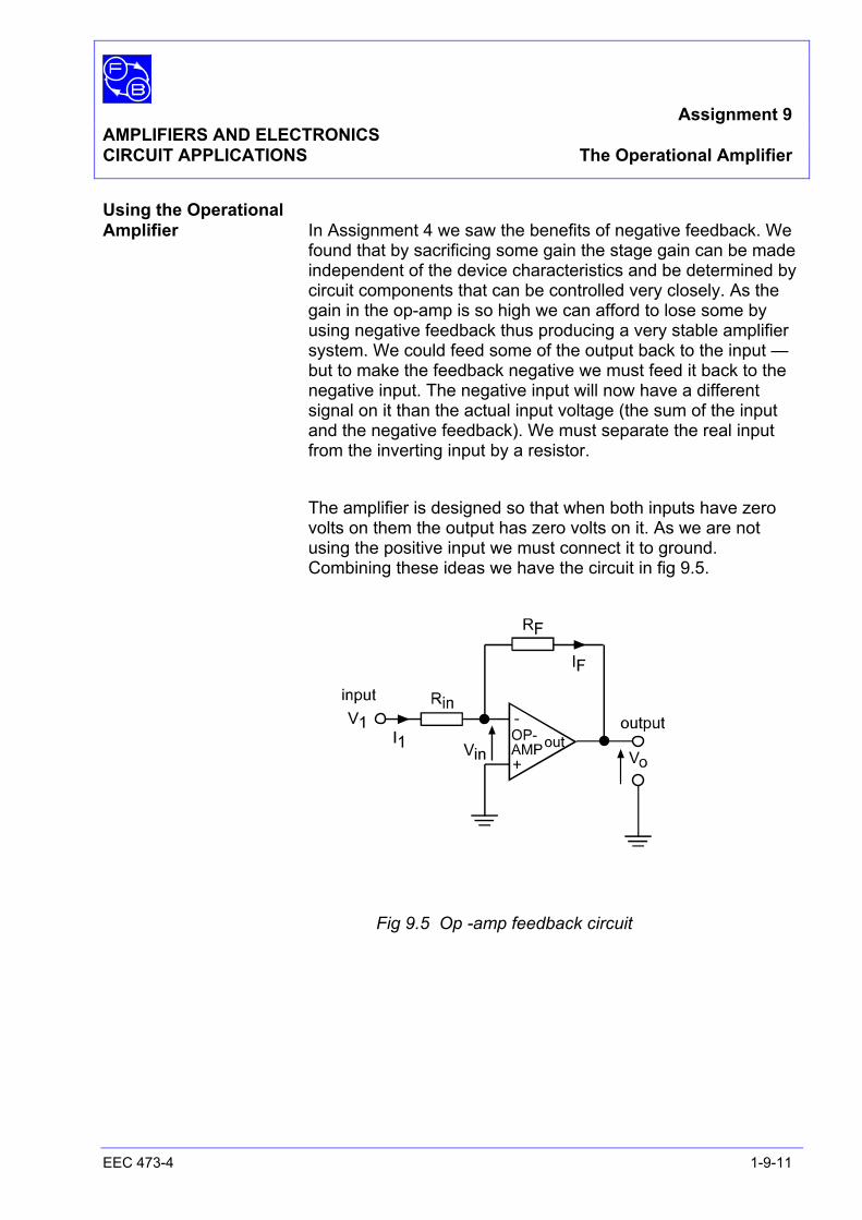
Assignment 9 AMPLIFIERS AND ELECTRONICS CIRCUIT APPLICATIONS The Operational Amplifier
EEC 473-4 1-9-11
Using the Operational Amplifier In Assignment 4 we saw the benefits of negative feedback. We
found that by sacrificing some gain the stage gain can be made independent of the device characteristics and be determined by circuit components that can be controlled very closely. As the gain in the op-amp is so high we can afford to lose some by using negative feedback thus producing a very stable amplifier system. We could feed some of the output back to the input — but to make the feedback negative we must feed it back to the negative input. The negative input will now have a different signal on it than the actual input voltage (the sum of the input and the negative feedback). We must separate the real input from the inverting input by a resistor.
The amplifier is designed so that when both inputs have zero
volts on them the output has zero volts on it. As we are not using the positive input we must connect it to ground. Combining these ideas we have the circuit in fig 9.5.
Fig 9.5 Op -amp feedback circuit
Assignment 9 AMPLIFIERS AND ELECTRONICS CIRCUIT APPLICATIONS The Operational Amplifier
EEC 473-4 1-9-12
We will now apply some simple theory to this circuit. We know that the gain of the op-amp is very high, so Vin will be
very small compared with Vo. If we assume it to be almost zero we can say:
Vo = – IF RF (very nearly)
∴ IF = −V oR F
but IF = I1 = VR in1
R
V
R
VI
in
1
F
0F
== −
∴R
R
V
V
in
F
1
0 −=
This is very important as we have produced an amplifier the gain of which is the ratio of two resistors, and is independent of the actual gain of the op-amp. This is called 'closed loop operation'. Notice that the amplifier inverts the signal.

Ass
ignm
ent 9
A
MPL
IFIE
RS
AN
D E
LEC
TRO
NIC
S
CIR
CU
IT A
PPLI
CA
TIO
NS
The
Ope
ratio
nal A
mpl
ifier
E
EC
473
-4
1-9-
13
Not
es
Assignment 9 AMPLIFIERS AND ELECTRONICS CIRCUIT APPLICATIONS The Operational Amplifier
EEC 473-4 1-9-14
Fig 9.7
Assignment 9 AMPLIFIERS AND ELECTRONICS CIRCUIT APPLICATIONS The Operational Amplifier
EEC 473-4 1-9-15
EXPERIMENTAL PROCEDURE The operational amplifier we shall be using for our experiments
is a type 741. It is very small, and comes in a plastic pack 9 mm x 6 mm x 3 mm. For convenience, the device is soldered on a small board with pins to suit the EEC470 deck. There are a few practical problems. Although in theory when both inputs are zero the output should be zero, due to leakage currents and other causes there is a slight 'offset' of the output. This can be removed by the offset null potentiometer mounted in the module.
In the first activity we shall familiarise ourselves with the IC and try the offset null control. In the second activity we shall make a closed-loop feedback circuit.
Dc Offset The circuit we shall use is shown in fig 9.6. Set up the layout in fig 9.7.
Note Operational amplifiers of the type used in the Kit require a fixed power supply of +15, 0, –15 V dc. This fixed supply is usually omitted from circuit diagrams showing operational amplifiers, in order to reduce the number of connections shown to the minimum necessary. The +15 V dc and –15 V dc connections to pins 12 and 9 respectively of the 741 Op–Amp on fig 9.5 are therefore omitted from fig 9.6 and subsequent diagrams.
Fig 9.6 Test circuit for dc offset
Assignment 9 AMPLIFIERS AND ELECTRONICS CIRCUIT APPLICATIONS The Operational Amplifier
EEC 473-4 1-9-16
Switch on the power supply. Turn the potentiometer, marked 'zero', in the op-amp module with a small screwdriver. Notice that the output changes between +15 volts and -15 volts very suddenly. It is not possible to set it to zero as the amplifier is operating in the open-loop mode with very high gain. The potentiometer is not fine enough in this condition. Now link A to B thus adding a 100 kohm feedback resistor. The loop is now closed and the gain reduced.
Questions 1 Can you calculate the gain? Try to null the amplifier again.
2 Can you set the output to zero? Why? One of the most common uses of the differential amplifier is in
the input circuits of an operational amplifier. It is this circuit that enables the amplifier to have an inverting and non-inverting input. The gain of the amplifier block is very high and is usually reduced using passive components to produce a precision set gain. There are many types available, a common general purpose type is the 741, the characteristics of which are shown below:
Supply, voltage = ±18 volts max.
Gain (f = 1Hz) = 5 x 10⁵
Gain (f = 100kHz) = 10 Output impedance = 300 ohms (approx)
Input impedance = 1 MΩ CMRR = 90 db In the following applications the operational amplifier is used to
perform a range of functions widely used in industrial electronics.

Ass
ignm
ent 9
A
MPL
IFIE
RS
AN
D E
LEC
TRO
NIC
S
CIR
CU
IT A
PPLI
CA
TIO
NS
The
Ope
ratio
nal A
mpl
ifier
E
EC
473
-4
1-9-
17
Not
es
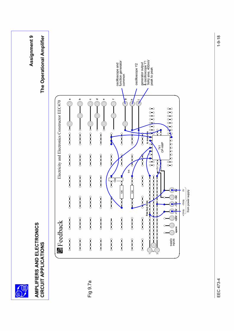
Ass
ignm
ent 9
A
MPL
IFIE
RS
AN
D E
LEC
TRO
NIC
S
CIR
CU
IT A
PPLI
CA
TIO
NS
The
Ope
ratio
nal A
mpl
ifier
E
EC
473
-4
1-9-
18
Fi
g 9.
7a
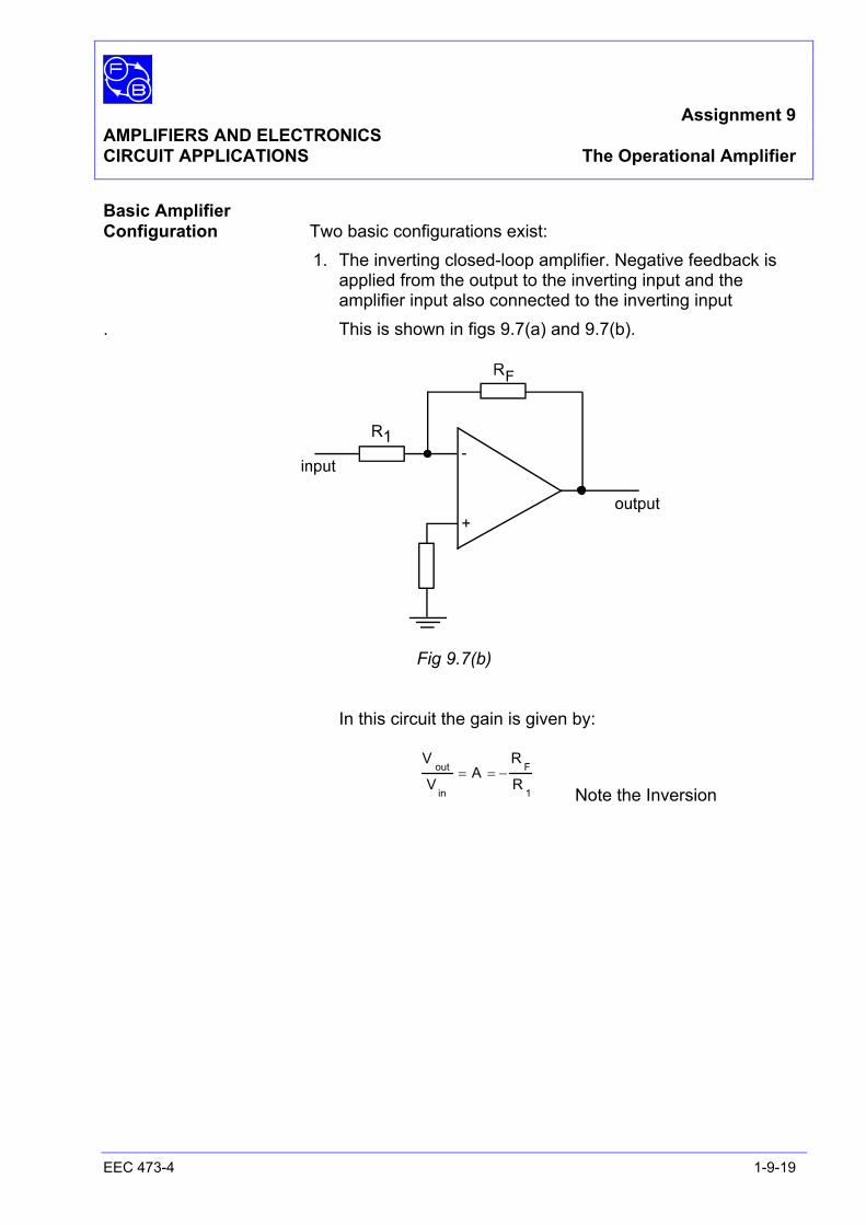
Assignment 9 AMPLIFIERS AND ELECTRONICS CIRCUIT APPLICATIONS The Operational Amplifier
EEC 473-4 1-9-19
Basic Amplifier Configuration Two basic configurations exist: 1. The inverting closed-loop amplifier. Negative feedback is applied from the output to the inverting input and the amplifier input also connected to the inverting input . This is shown in figs 9.7(a) and 9.7(b).
Fig 9.7(b) In this circuit the gain is given by:
Vout
Vin
= A = −R
F
R1 Note the Inversion

Assignment 9 AMPLIFIERS AND ELECTRONICS CIRCUIT APPLICATIONS The Operational Amplifier
EEC 473-4 1-9-20
Notes

Ass
ignm
ent 9
A
MPL
IFIE
RS
AN
D E
LEC
TRO
NIC
S
CIR
CU
IT A
PPLI
CA
TIO
NS
The
Ope
ratio
nal A
mpl
ifier
E
EC
473
-4
1-9-
21
Not
es
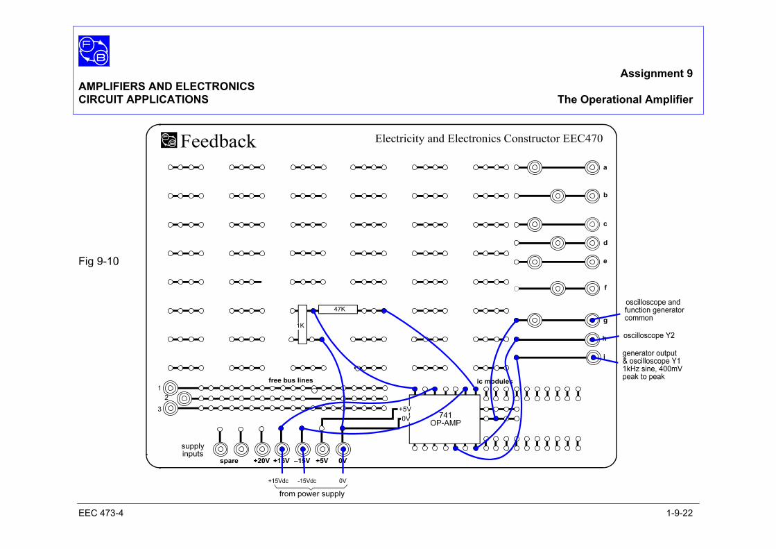
Assignment 9 AMPLIFIERS AND ELECTRONICS CIRCUIT APPLICATIONS The Operational Amplifier
EEC 473-4 1-9-22
Fig 9-10
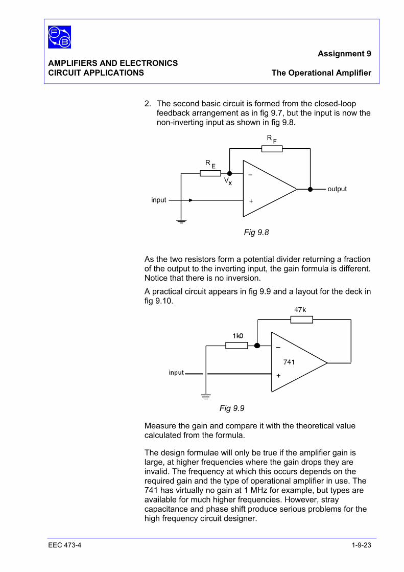
Assignment 9 AMPLIFIERS AND ELECTRONICS CIRCUIT APPLICATIONS The Operational Amplifier
EEC 473-4 1-9-23
2. The second basic circuit is formed from the closed-loop feedback arrangement as in fig 9.7, but the input is now the non-inverting input as shown in fig 9.8.
Fig 9.8 As the two resistors form a potential divider returning a fraction
of the output to the inverting input, the gain formula is different. Notice that there is no inversion.
A practical circuit appears in fig 9.9 and a layout for the deck in fig 9.10.
Fig 9.9
Measure the gain and compare it with the theoretical value calculated from the formula.
The design formulae will only be true if the amplifier gain is large, at higher frequencies where the gain drops they are invalid. The frequency at which this occurs depends on the required gain and the type of operational amplifier in use. The 741 has virtually no gain at 1 MHz for example, but types are available for much higher frequencies. However, stray capacitance and phase shift produce serious problems for the high frequency circuit designer.
Assignment 9 AMPLIFIERS AND ELECTRONICS CIRCUIT APPLICATIONS The Operational Amplifier
EEC 473-4 1-9-24
PRACTICAL CONSIDERATIONS AND APPLICATIONS
The 741 is a general-purpose op-amp; there are others which have higher input impedances and work up to a higher frequency. Although the 741 is quite insensitive to supply voltage variations it is normally used with a regulated supply.
SUMMARY In this assignment you have learnt that : 1 The operational amplifier is a dc amplifier which can
amplify both positive and negative signals and give positive or negative outputs.
2 The amplifier has a differential input and very high gain.
3 When operated in a closed loop the gain can be very closely
controlled by resistors.
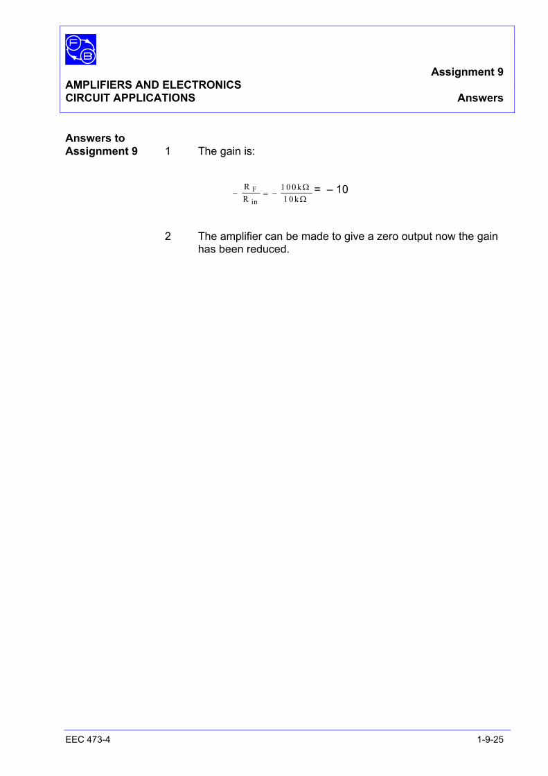
Assignment 9 AMPLIFIERS AND ELECTRONICS CIRCUIT APPLICATIONS Answers
EEC 473-4 1-9-25
Answers to Assignment 9 1 The gain is:
− = −RR
kk
F
in
1 0 01 0
ΩΩ
= – 10
2 The amplifier can be made to give a zero output now the gain has been reduced.

Assignment 9 AMPLIFIERS AND ELECTRONICS CIRCUIT APPLICATIONS Answers
EEC 473-4 1-9-26
Notes
Assignment 10 AMPLIFIERS AND ELECTRONICS CIRCUIT APPLICATIONS The Operational Amplifier Applications
EEC 473-4 1-10-1
OBJECTIVES 1. An understanding of operational amplifier’s use as a summing amplifier.
2. An understanding of operational amplifier’s use as a voltage follower.
3. An understanding of operational amplifier’s use as a comparator.
4. An understanding of operational amplifier’s use as an integrator.
EQUIPMENT REQUIRED Qty Apparatus 1 Electricity & Electronics Constructor EEC470 1 Amplifier Kit EEC473-4 1 Power supply unit 0 to +20 V variable dc and ±15 V dc. regulated (eg, Feedback Power Supply 92-445 or 92-100 Teknikit Console) 1 Function generator sinewave 1V at 1 kHz (eg, Feedback FG601) 2 Multimeters or 2 Voltmeters 15 V dc 1 2-Channel oscilloscope PREREQUISITES Assignment 9 KNOWLEDGE LEVEL See prerequisites
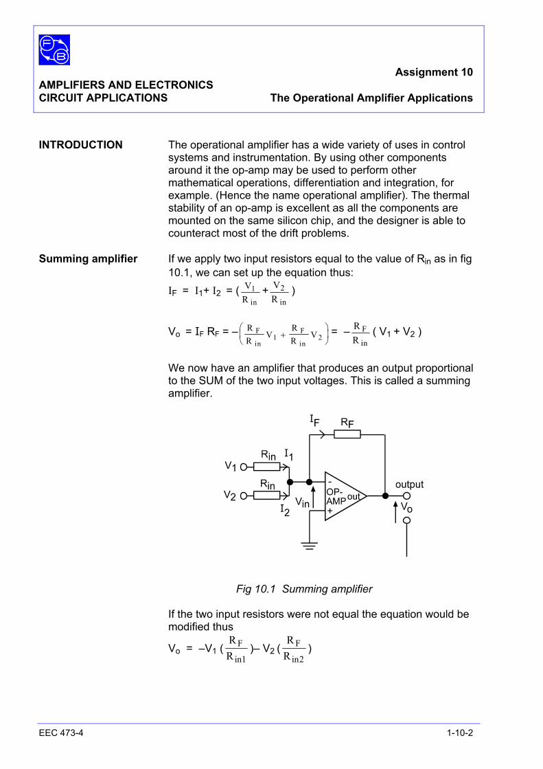
Assignment 10 AMPLIFIERS AND ELECTRONICS CIRCUIT APPLICATIONS The Operational Amplifier Applications
EEC 473-4 1-10-2
INTRODUCTION The operational amplifier has a wide variety of uses in control
systems and instrumentation. By using other components around it the op-amp may be used to perform other mathematical operations, differentiation and integration, for example. (Hence the name operational amplifier). The thermal stability of an op-amp is excellent as all the components are mounted on the same silicon chip, and the designer is able to counteract most of the drift problems.
Summing amplifier If we apply two input resistors equal to the value of Rin as in fig
10.1, we can set up the equation thus: IF = I1+ I2 = ( V
R in1 + V
R in2 )
Vo = IF RF = – R
RV
RR
VF
in
F
in1 2+
= – R
RF
in( V1 + V2 )
We now have an amplifier that produces an output proportional
to the SUM of the two input voltages. This is called a summing amplifier.
Fig 10.1 Summing amplifier If the two input resistors were not equal the equation would be
modified thus
Vo = –V1 (RRF
in1)– V2 (
RRF
in2)

Ass
ignm
ent 1
0 A
MPL
IFIE
RS
AN
D E
LEC
TRO
NIC
S
CIR
CU
IT A
PPLI
CA
TIO
NS
The
Ope
ratio
nal A
mpl
ifier
App
licat
ions
E
EC
473
-4
1-10
-3
Not
es
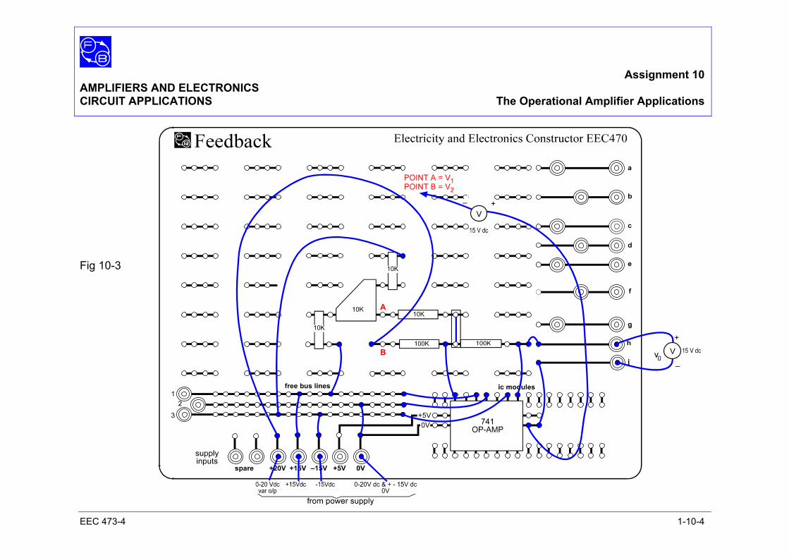
Assignment 10 AMPLIFIERS AND ELECTRONICS CIRCUIT APPLICATIONS The Operational Amplifier Applications
EEC 473-4 1-10-4
Fig 10-3
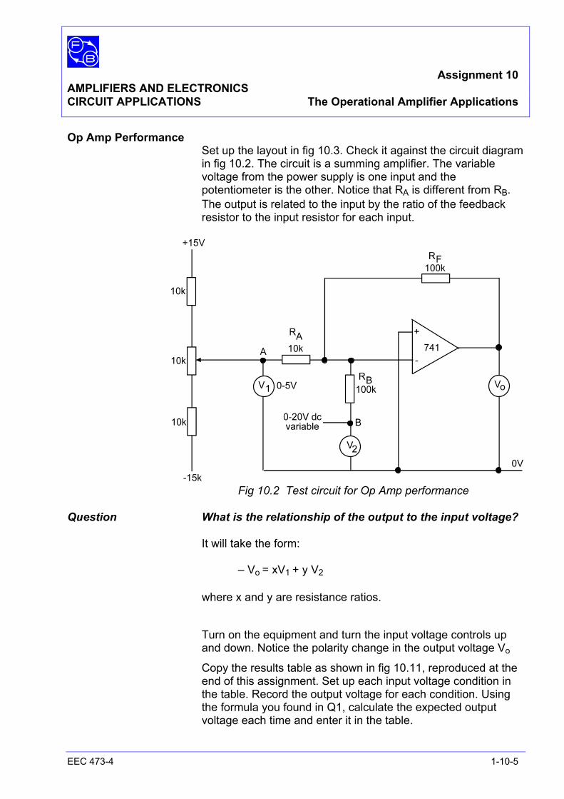
Assignment 10 AMPLIFIERS AND ELECTRONICS CIRCUIT APPLICATIONS The Operational Amplifier Applications
EEC 473-4 1-10-5
Op Amp Performance Set up the layout in fig 10.3. Check it against the circuit diagram
in fig 10.2. The circuit is a summing amplifier. The variable voltage from the power supply is one input and the potentiometer is the other. Notice that RA is different from RB. The output is related to the input by the ratio of the feedback resistor to the input resistor for each input.
Fig 10.2 Test circuit for Op Amp performance Question What is the relationship of the output to the input voltage? It will take the form: – Vo = xV1 + y V2 where x and y are resistance ratios. Turn on the equipment and turn the input voltage controls up
and down. Notice the polarity change in the output voltage Vo
Copy the results table as shown in fig 10.11, reproduced at the end of this assignment. Set up each input voltage condition in the table. Record the output voltage for each condition. Using the formula you found in Q1, calculate the expected output voltage each time and enter it in the table.
Assignment 10 AMPLIFIERS AND ELECTRONICS CIRCUIT APPLICATIONS The Operational Amplifier Applications
EEC 473-4 1-10-6
We have made an electronic adding machine as the output voltage is the algebraic sum of the input voltages. It uses electric current as an analogue of the number. There are larger systems using this principle and they are called analogue computers.

Ass
ignm
ent 1
0 A
MPL
IFIE
RS
AN
D E
LEC
TRO
NIC
S
CIR
CU
IT A
PPLI
CA
TIO
NS
The
Ope
ratio
nal A
mpl
ifier
App
licat
ions
E
EC
473
-4
1-10
-7
Not
es
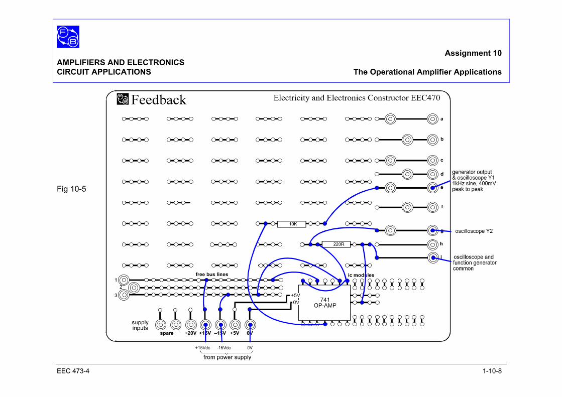
Assignment 10 AMPLIFIERS AND ELECTRONICS CIRCUIT APPLICATIONS The Operational Amplifier Applications
EEC 473-4 1-10-8
Fig 10-5
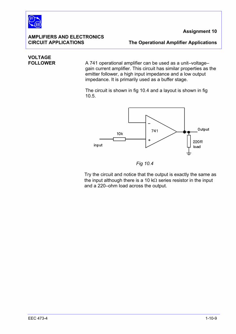
Assignment 10 AMPLIFIERS AND ELECTRONICS CIRCUIT APPLICATIONS The Operational Amplifier Applications
EEC 473-4 1-10-9
VOLTAGE FOLLOWER A 741 operational amplifier can be used as a unit–voltage– gain current amplifier. This circuit has similar properties as the emitter follower, a high input impedance and a low output impedance. It is primarily used as a buffer stage. The circuit is shown in fig 10.4 and a layout is shown in fig 10.5.
Fig 10.4 Try the circuit and notice that the output is exactly the same as
the input although there is a 10 kΩ series resistor in the input and a 220–ohm load across the output.

Assignment 10 AMPLIFIERS AND ELECTRONICS CIRCUIT APPLICATIONS The Operational Amplifier Applications
EEC 473-4 1-10-10
Notes

Ass
ignm
ent 1
0 A
MPL
IFIE
RS
AN
D E
LEC
TRO
NIC
S
CIR
CU
IT A
PPLI
CA
TIO
NS
The
Ope
ratio
nal A
mpl
ifier
App
licat
ions
E
EC
473
-4
1-10
-11
N
otes
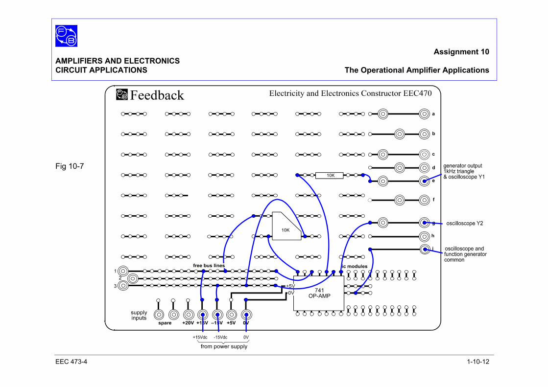
Assignment 10 AMPLIFIERS AND ELECTRONICS CIRCUIT APPLICATIONS The Operational Amplifier Applications
EEC 473-4 1-10-12
Fig 10-7
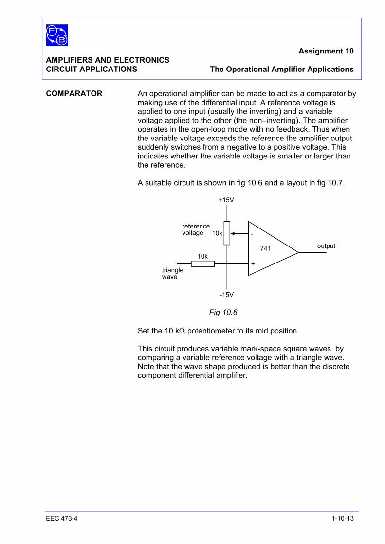
Assignment 10 AMPLIFIERS AND ELECTRONICS CIRCUIT APPLICATIONS The Operational Amplifier Applications
EEC 473-4 1-10-13
COMPARATOR An operational amplifier can be made to act as a comparator by making use of the differential input. A reference voltage is applied to one input (usually the inverting) and a variable voltage applied to the other (the non–inverting). The amplifier operates in the open-loop mode with no feedback. Thus when the variable voltage exceeds the reference the amplifier output suddenly switches from a negative to a positive voltage. This indicates whether the variable voltage is smaller or larger than the reference.
A suitable circuit is shown in fig 10.6 and a layout in fig 10.7.
Fig 10.6 Set the 10 kΩ potentiometer to its mid position This circuit produces variable mark-space square waves by
comparing a variable reference voltage with a triangle wave. Note that the wave shape produced is better than the discrete component differential amplifier.
Assignment 10 AMPLIFIERS AND ELECTRONICS CIRCUIT APPLICATIONS The Operational Amplifier Applications
EEC 473-4 1-10-14
Notes

Ass
ignm
ent 1
0 A
MPL
IFIE
RS
AN
D E
LEC
TRO
NIC
S
CIR
CU
IT A
PPLI
CA
TIO
NS
The
Ope
ratio
nal A
mpl
ifier
App
licat
ions
E
EC
473
-4
1-10
-15
Not
es
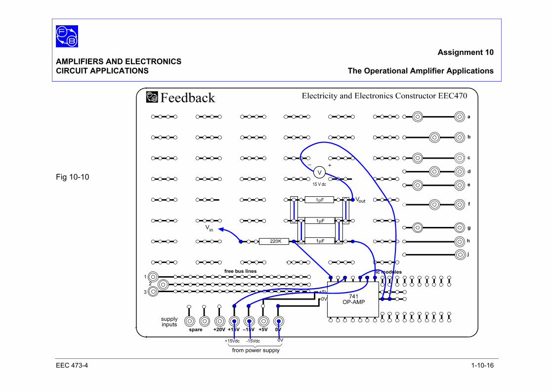
Assignment 10 AMPLIFIERS AND ELECTRONICS CIRCUIT APPLICATIONS The Operational Amplifier Applications
EEC 473-4 1-10-16
Fig 10-10
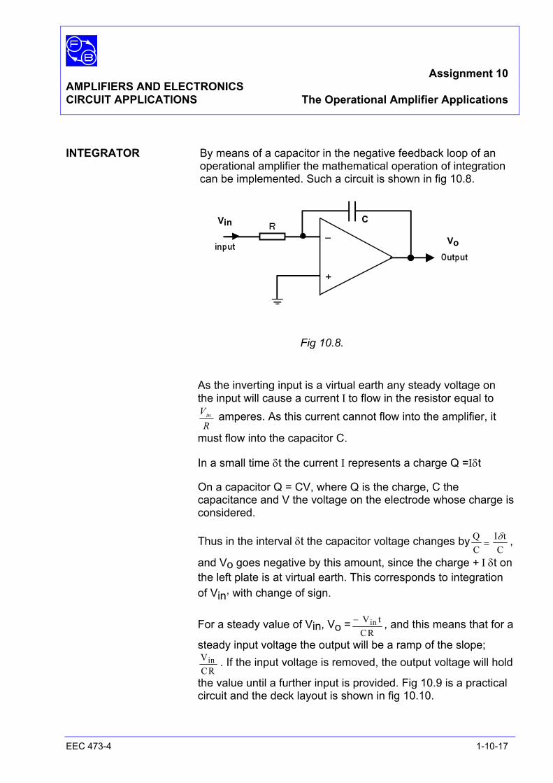
Assignment 10 AMPLIFIERS AND ELECTRONICS CIRCUIT APPLICATIONS The Operational Amplifier Applications
EEC 473-4 1-10-17
INTEGRATOR By means of a capacitor in the negative feedback loop of an operational amplifier the mathematical operation of integration can be implemented. Such a circuit is shown in fig 10.8.
Fig 10.8.
As the inverting input is a virtual earth any steady voltage on the input will cause a current I to flow in the resistor equal to
RVin amperes. As this current cannot flow into the amplifier, it
must flow into the capacitor C.
In a small time δt the current I represents a charge Q =Ιδt
On a capacitor Q = CV, where Q is the charge, C the capacitance and V the voltage on the electrode whose charge is considered.
Thus in the interval δt the capacitor voltage changes by QC
I tC
=δ ,
and Vo goes negative by this amount, since the charge + I δt on the left plate is at virtual earth. This corresponds to integration of Vin, with change of sign.
For a steady value of Vin, Vo = − V tCR
in , and this means that for a
steady input voltage the output will be a ramp of the slope; VCR
in . If the input voltage is removed, the output voltage will hold
the value until a further input is provided. Fig 10.9 is a practical circuit and the deck layout is shown in fig 10.10.
Vo
CVin
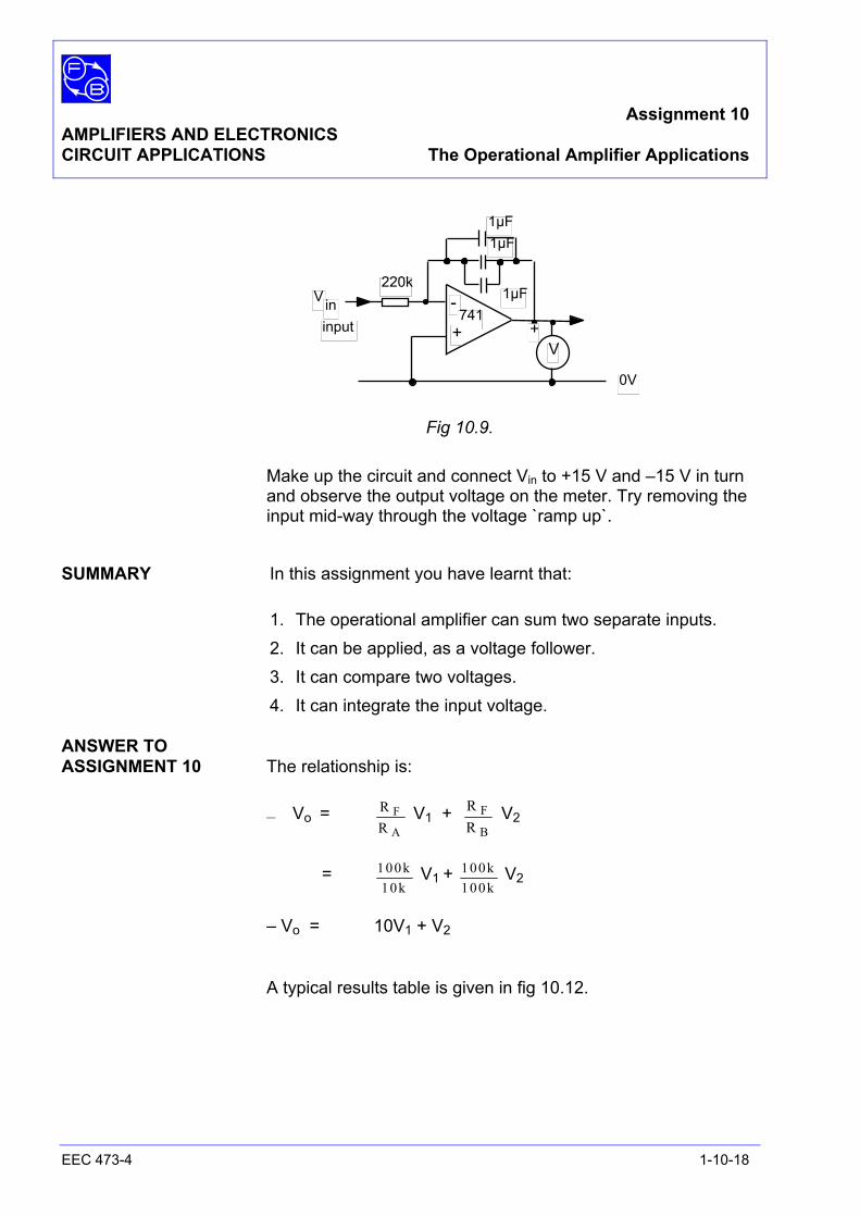
Assignment 10 AMPLIFIERS AND ELECTRONICS CIRCUIT APPLICATIONS The Operational Amplifier Applications
EEC 473-4 1-10-18
Fig 10.9. Make up the circuit and connect Vin to +15 V and –15 V in turn
and observe the output voltage on the meter. Try removing the input mid-way through the voltage `ramp up`.
SUMMARY In this assignment you have learnt that:
1. The operational amplifier can sum two separate inputs. 2. It can be applied, as a voltage follower. 3. It can compare two voltages. 4. It can integrate the input voltage. ANSWER TO ASSIGNMENT 10 The relationship is:
– Vo = RR
F
A V1 + R
RF
B V2
= 100
10k
k V1 + 100
100kk
V2
– Vo = 10V1 + V2 A typical results table is given in fig 10.12.
-
+ input
1µF 1µF
1µF 741
V +
220k V in
0V
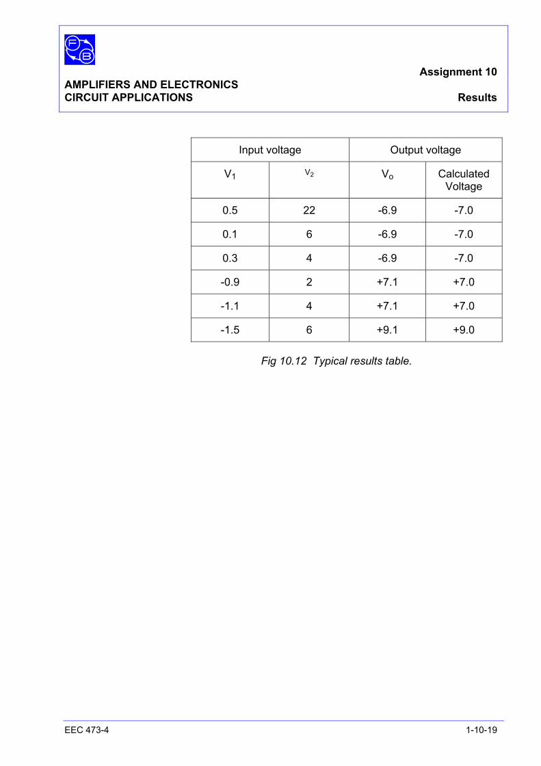
Assignment 10 AMPLIFIERS AND ELECTRONICS CIRCUIT APPLICATIONS Results
EEC 473-4 1-10-19
Input voltage Output voltage
V1 V2 Vo Calculated Voltage
0.5 22 -6.9 -7.0
0.1 6 -6.9 -7.0
0.3 4 -6.9 -7.0
-0.9 2 +7.1 +7.0
-1.1 4 +7.1 +7.0
-1.5 6 +9.1 +9.0
Fig 10.12 Typical results table.

Assignment 10 AMPLIFIERS AND ELECTRONICS CIRCUIT APPLICATIONS Results
EEC 473-4 1-10-20
Notes
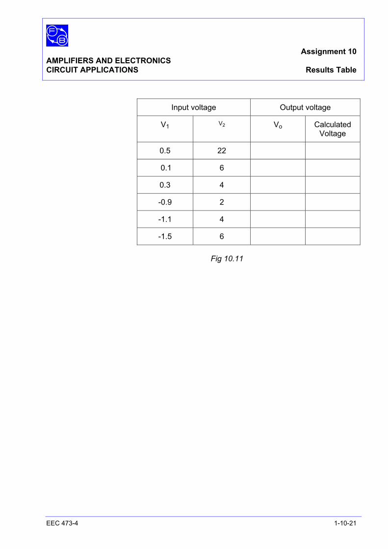
Assignment 10 AMPLIFIERS AND ELECTRONICS CIRCUIT APPLICATIONS Results Table
EEC 473-4 1-10-21
Input voltage Output voltage
V1 V2 Vo Calculated Voltage
0.5 22
0.1 6
0.3 4
-0.9 2
-1.1 4
-1.5 6
Fig 10.11

Assignment 10 AMPLIFIERS AND ELECTRONICS CIRCUIT APPLICATIONS Results Table
EEC 473-4 1-10-22
Notes
Section 2 AMPLIFIERS AND ELECTRONIC CIRCUIT APPLICATIONS Oscillators
EEC 473-4 2-1
Oscillators Oscillators are used in many electronics systems often providing the central 'clock' that controls the sequential operation of the entire system. They are used in many pieces of test equipment in one form or another, and over a very wide range of frequencies. They can produce a very wide range of wave shapes and can be quite complicated or quite simple depending on the application.
In the following notes some of the basic oscillators are shown. The deficiencies of these simple circuits will often be obvious from their output waveshape.

Section 2 AMPLIFIERS AND ELECTRONIC CIRCUIT APPLICATIONS Oscillators
EEC 473-4 2-2
Notes
Assignment 11 AMPLIFIERS AND ELECTRONIC CIRCUIT APPLICATIONS The Phase Shift Oscillator
EEC 473-4 2-11-1
EQUIPMENT REQUIRED Qty Apparatus 1 Electricity & Electronics Constructor EEC470 1 Circuit Applications Kit EEC473-4 1 Power supply unit +15 V dc regulated
(eg, Feedback Power Supply 92-445 or 92-100 Teknikit Console)
1 2–Channel oscilloscope PREREQUISITES Assignment 6 KNOWLEDGE LEVEL Before working this Application you should :
• Know how the positive and negative feedback loops can be applied to Common Emitter amplifier circuits.
Assignment 11 AMPLIFIERS AND ELECTRONIC CIRCUIT APPLICATIONS The Phase Shift Oscillator
EEC 473-4 2-11-2
Notes

Ass
ignm
ent 1
1 A
MPL
IFIE
RS
AN
D E
LEC
TRO
NIC
CIR
CU
IT A
PPLI
CA
TIO
NS
The
Phas
e Sh
ift O
scill
ator
E
EC
473
-4
2-11
-3
Not
es
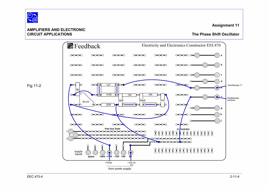
Assignment 11 AMPLIFIERS AND ELECTRONIC CIRCUIT APPLICATIONS The Phase Shift Oscillator
EEC 473-4 2-11-4
Fig 11-2
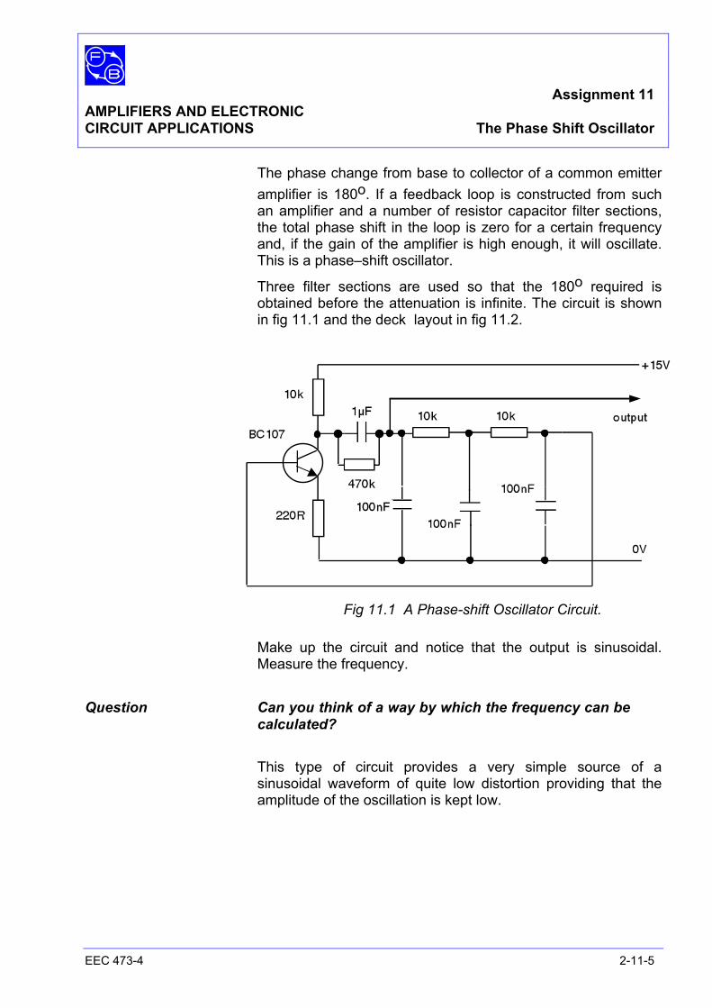
Assignment 11 AMPLIFIERS AND ELECTRONIC CIRCUIT APPLICATIONS The Phase Shift Oscillator
EEC 473-4 2-11-5
The phase change from base to collector of a common emitter amplifier is 180o. If a feedback loop is constructed from such an amplifier and a number of resistor capacitor filter sections, the total phase shift in the loop is zero for a certain frequency and, if the gain of the amplifier is high enough, it will oscillate. This is a phase–shift oscillator.
Three filter sections are used so that the 180o required is obtained before the attenuation is infinite. The circuit is shown in fig 11.1 and the deck layout in fig 11.2.
Fig 11.1 A Phase-shift Oscillator Circuit. Make up the circuit and notice that the output is sinusoidal.
Measure the frequency. Question Can you think of a way by which the frequency can be
calculated? This type of circuit provides a very simple source of a
sinusoidal waveform of quite low distortion providing that the amplitude of the oscillation is kept low.
Assignment 11 AMPLIFIERS AND ELECTRONIC CIRCUIT APPLICATIONS The Phase Shift Oscillator
EEC 473-4 2-11-6
Answer to question in Assignment 11 By using vector diagrams or mathematics the phase shift of the
network can be calculated, thus by calculating at what frequency the phase shift is 180o the frequency of oscillation can be predicted. The mathematics are, however, outside the scope of this book.
Assignment 12 AMPLIFIERS AND ELECTRONIC CIRCUIT APPLICATIONS The Astable Multivibrator and its Application
EEC 473-4 2-12-1
EQUIPMENT REQUIRED Qty Apparatus 1 Electricity & Electronics Constructor
EEC470 1 Circuit Applications Kit EEC473-4 1 Power supply unit +5 V dc regulated
(eg, Feedback Power Supply 92-445 or 92-100 Teknikit Console)
1 2–Channel oscilloscope PREREQUISITES Assignment 10 KNOWLEDGE LEVEL Before considering on this application you should
• Know the operation of the Common Emitter amplifier circuit.
Assignment 12 AMPLIFIERS AND ELECTRONIC CIRCUIT APPLICATIONS The Astable Multivibrator and its Application
EEC 473-4 2-12-2
Notes

Ass
ignm
ent 1
2 A
MPL
IFIE
RS
AN
D E
LEC
TRO
NIC
CIR
CU
IT A
PPLI
CA
TIO
NS
The
Ast
able
Mul
tivib
rato
r and
its
App
licat
ion
EE
C 4
73-4
2-
12-3
Not
es
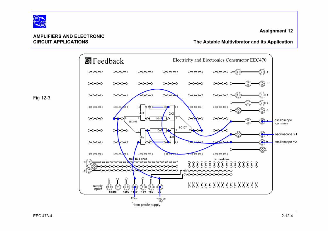
Assignment 12 AMPLIFIERS AND ELECTRONIC CIRCUIT APPLICATIONS The Astable Multivibrator and its Application
EEC 473-4 2-12-4
Fig 12-3
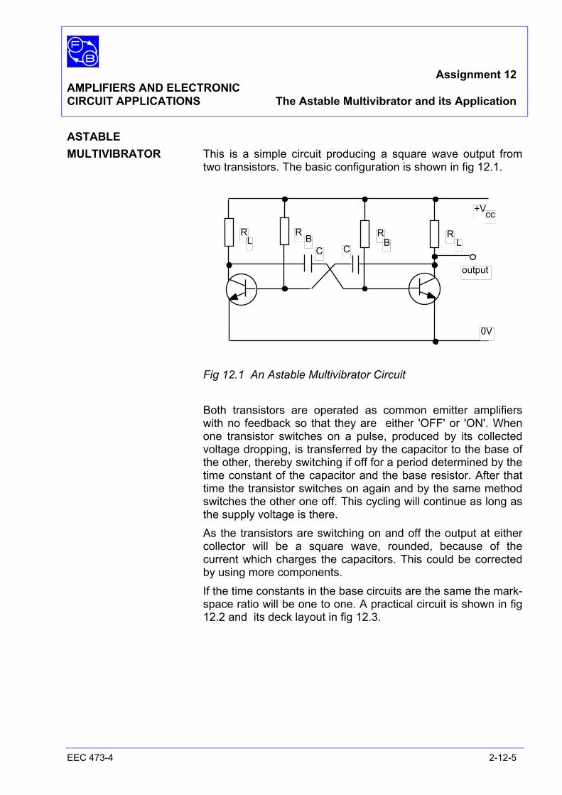
Assignment 12 AMPLIFIERS AND ELECTRONIC CIRCUIT APPLICATIONS The Astable Multivibrator and its Application
EEC 473-4 2-12-5
ASTABLE MULTIVIBRATOR This is a simple circuit producing a square wave output from
two transistors. The basic configuration is shown in fig 12.1.
Fig 12.1 An Astable Multivibrator Circuit
Both transistors are operated as common emitter amplifiers with no feedback so that they are either 'OFF' or 'ON'. When one transistor switches on a pulse, produced by its collected voltage dropping, is transferred by the capacitor to the base of the other, thereby switching if off for a period determined by the time constant of the capacitor and the base resistor. After that time the transistor switches on again and by the same method switches the other one off. This cycling will continue as long as the supply voltage is there.
As the transistors are switching on and off the output at either collector will be a square wave, rounded, because of the current which charges the capacitors. This could be corrected by using more components.
If the time constants in the base circuits are the same the mark-space ratio will be one to one. A practical circuit is shown in fig 12.2 and its deck layout in fig 12.3.
R L
R B R
B R
L
+V cc
output
0V
C C
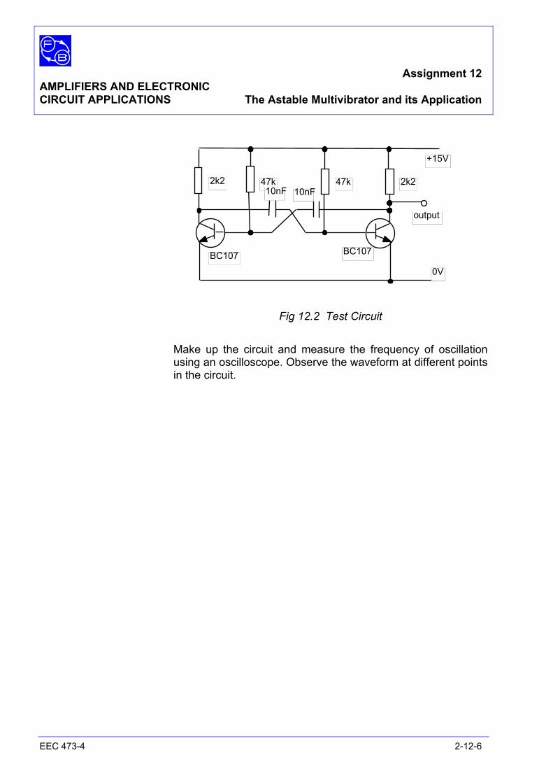
Assignment 12 AMPLIFIERS AND ELECTRONIC CIRCUIT APPLICATIONS The Astable Multivibrator and its Application
EEC 473-4 2-12-6
Fig 12.2 Test Circuit
Make up the circuit and measure the frequency of oscillation using an oscilloscope. Observe the waveform at different points in the circuit.
output
0V
2k2 47k 47k 2k2
BC107 BC107
10nF 10nF
+15V
Ass
ignm
ent 1
2 A
MPL
IFIE
RS
AN
D E
LEC
TRO
NIC
CIR
CU
IT A
PPLI
CA
TIO
NS
The
Ast
able
Mul
tivib
rato
r and
its
App
licat
ion
EE
C 4
73-4
2-
12-7
N
otes
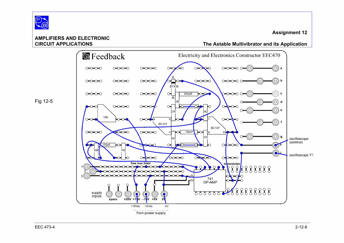
Assignment 12 AMPLIFIERS AND ELECTRONIC CIRCUIT APPLICATIONS The Astable Multivibrator and its Application
EEC 473-4 2-12-8
Fig 12-5
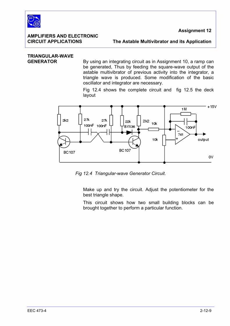
Assignment 12 AMPLIFIERS AND ELECTRONIC CIRCUIT APPLICATIONS The Astable Multivibrator and its Application
EEC 473-4 2-12-9
TRIANGULAR-WAVE GENERATOR By using an integrating circuit as in Assignment 10, a ramp can
be generated, Thus by feeding the square-wave output of the astable multivibrator of previous activity into the integrator, a triangle wave is produced. Some modification of the basic oscillator and integrator are necessary.
Fig 12.4 shows the complete circuit and fig 12.5 the deck layout
Fig 12.4 Triangular-wave Generator Circuit.
Make up and try the circuit. Adjust the potentiometer for the best triangle shape.
This circuit shows how two small building blocks can be brought together to perform a particular function.

Assignment 12 AMPLIFIERS AND ELECTRONIC CIRCUIT APPLICATIONS The Astable Multivibrator and its Application
EEC 473-4 2-12-10
Notes
Assignment 13 AMPLIFIERS AND ELECTRONIC CIRCUIT APPLICATIONS A Unijunction Pulse–Generator and its Application
EEC 473-4 2-13-1
EQUIPMENT REQUIRED Qty Apparatus 1 Electricity & Electronics Constructor EEC470 1 Circuit Applications Kit EEC473-4 1 Power supply unit +15 V dc regulated
(eg, Feedback Power Supply 92-445 or 92-100 Teknikit Console)
1 Function generator, 100 kHz 4 V pk–pk squarewave (eg, Feedback FG601)
1 2–Channel oscilloscope PREREQUISITES Assignment 6 KNOWLEDGE LEVEL Before considering this Application you should : 1 Know the working of a Unijunction Transistor

Assignment 13 AMPLIFIERS AND ELECTRONIC CIRCUIT APPLICATIONS A Unijunction Pulse–Generator and its Application
EEC 473-4 2-13-2
Notes
Ass
ignm
ent 1
3 A
MPL
IFIE
RS
AN
D E
LEC
TRO
NIC
CIR
CU
IT A
PPLI
CA
TIO
NS
A U
niju
nctio
n Pu
lse–
Gen
erat
or a
nd it
s A
pplic
atio
n E
EC
473
-4
2-13
-3
Not
es
Assignment 13 AMPLIFIERS AND ELECTRONIC CIRCUIT APPLICATIONS A Unijunction Pulse–Generator and its Application
EEC 473-4 2-13-4
Fig 13-3
Assignment 13 AMPLIFIERS AND ELECTRONIC CIRCUIT APPLICATIONS A Unijunction Pulse–Generator and its Application
EEC 473-4 2-13-5
The unijunction transistor can be used as a voltage–operated switch to produce a pulse-generator circuit as shown in fig 13.1.
Fig13.1 A Unijunction Pulse Generator Circuit.
The time between each pulse is set by the time that the
capacitor takes to recharge. The small output pulse from B1 on the unijunction switches the transistor on and produces a negative pulse at the output.
The expected waveshape is shown in fig 13.2 below, and the deck layout of the circuit in fig 13.3.
Fig 13.2 A Typical Waveshape. Try different values of capacitor and notice the effect of the
pulse repetition rate.
+15V
0V time

Assignment 13 AMPLIFIERS AND ELECTRONIC CIRCUIT APPLICATIONS A Unijunction Pulse–Generator and its Application
EEC 473-4 2-13-6
Notes

Ass
ignm
ent 1
3 A
MPL
IFIE
RS
AN
D E
LEC
TRO
NIC
CIR
CU
IT A
PPLI
CA
TIO
NS
A U
niju
nctio
n Pu
lse–
Gen
erat
or a
nd it
s A
pplic
atio
n E
EC
473
-4
2-13
-7
Not
es
Assignment 13 AMPLIFIERS AND ELECTRONIC CIRCUIT APPLICATIONS A Unijunction Pulse–Generator and its Application
EEC 473-4 2-13-8
Fig 13-6
AMPLIFIERS AND ELECTRONIC Assignment 13 CIRCUIT APPLICATIONS A Unijunction Pulse–Generator and its Application
EEC 473-4 2-13-9
STAIRCASE GENERATOR This circuit uses a unijunction transistor switch to discharge a
capacitor when the voltage across it reaches a certain value. The capacitor is charged by short pulses derived from a square wave input. During the time between pulses, the emitter follower (used to produce sufficient current to charge the capacitor in a short time) is switched off, thus the capacitor holds its charge until either; another charge pulse, or the unijunction discharges it. The circuit is shown in fig 13.4 and the deck layout in fig 13.6.
Fig 13.4 A Staircase Generator Circuit.
Typical waveforms are shown in fig 13.5.
Fig 13.5 Typical Waveforms.
AMPLIFIERS AND ELECTRONIC Assignment 13 CIRCUIT APPLICATIONS A Unijunction Pulse–Generator and its Application
EEC 473-4 2-13-10
Initially set the function generator for a square wave output of 4 V peak-to-peak at a frequency of 1 kHz. Vary the frequency between 100 Hz and 1 kHz and observe the effect on the number of steps and note the repetition frequency of the staircase. With the frequency set to 1 kHz change the capacitor value, by connecting another 1 µF capacitor in parallel with the existing one to 2 µF and observe the effect on the repetition frequency. Vary the frequency between 100 Hz and 1 kHz and note the change in the number of steps.
Question Comment on the 'staircase' waveform with particular
emphasis on the effect of frequency changes in the amplitude of the square–wave input.
AMPLIFIERS AND ELECTRONIC Assignment 13 CIRCUIT APPLICATIONS Answers
EEC 473-4 2-13-11
Answer to Question in Assignment 13 The amplitude of the input square wave changes the mark–
space ratio of the charging pulse. If the charging pulse is longer, then the voltage rise across the capacitor during each pulse is greater. The number of steps therefore, required to reach the unijunction discharge voltage is smaller.
AMPLIFIERS AND ELECTRONIC Assignment 13 CIRCUIT APPLICATIONS Answers
EEC 473-4 2-13-12
Notes
AMPLIFIERS AND ELECTRONIC Assignment 14 CIRCUIT APPLICATIONS Timer Circuits
EEC 473-4 2-14-1
OBJECTIVES 1 An understanding of the operation and the use of a typical timer integrated circuit. 2 An understanding of monostable and astable circuits using such a device.
EQUIPMENT REQUIRED Qty Apparatus 1 Electricity & Electronics Constructor EEC470 1 Amplifier Kit EEC473-4 1 Power supply unit +15 V dc regulated
(eg, Feedback Power Supply 92-445 or 92-100 Teknikit Console)
PREREQUISITES Assignment 12 KNOWLEDGE LEVEL See prerequisite assignments
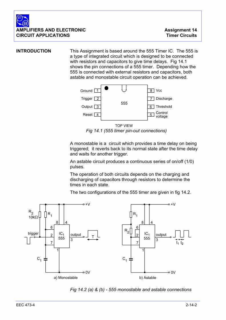
AMPLIFIERS AND ELECTRONIC Assignment 14 CIRCUIT APPLICATIONS Timer Circuits
EEC 473-4 2-14-2
INTRODUCTION This Assignment is based around the 555 Timer IC. The 555 is
a type of integrated circuit which is designed to be connected with resistors and capacitors to give time delays. Fig 14.1 shows the pin connections of a 555 timer. Depending how the 555 is connected with external resistors and capacitors, both astable and monostable circuit operation can be achieved.
Fig 14.1 (555 timer pin-out connections) A monostable is a circuit which provides a time delay on being
triggered; it reverts back to its normal state after the time delay and waits for another trigger. An astable circuit produces a continuous series of on/off (1/0) pulses. The operation of both circuits depends on the charging and discharging of capacitors through resistors to determine the times in each state.
The two configurations of the 555 timer are given in fig 14.2.
Fig 14.2 (a) & (b) - 555 monostable and astable connections
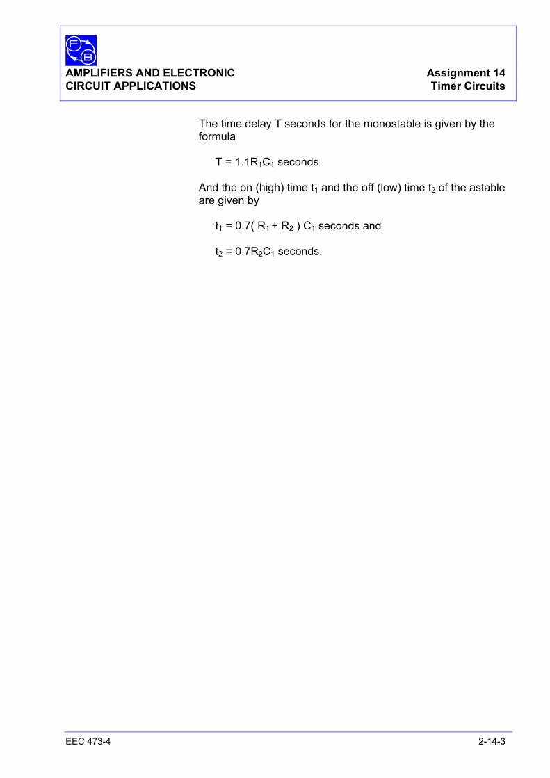
AMPLIFIERS AND ELECTRONIC Assignment 14 CIRCUIT APPLICATIONS Timer Circuits
EEC 473-4 2-14-3
The time delay T seconds for the monostable is given by the formula T = 1.1R1C1 seconds And the on (high) time t1 and the off (low) time t2 of the astable are given by t1 = 0.7( R1 + R2 ) C1 seconds and t2 = 0.7R2C1 seconds.

AMPLIFIERS AND ELECTRONIC Assignment 14 CIRCUIT APPLICATIONS Timer Circuits
EEC 473-4 2-14-4
Notes

A
MPL
IFIE
RS
AN
D E
LEC
TRO
NIC
A
ssig
nmen
t 14
CIR
CU
IT A
PPLI
CA
TIO
NS
Tim
er C
ircui
ts
EE
C 4
73-4
2-
14-5
N
otes
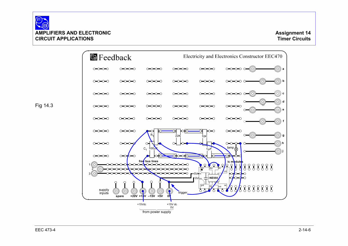
AMPLIFIERS AND ELECTRONIC Assignment 14 CIRCUIT APPLICATIONS Timer Circuits
EEC 473-4 2-14-6
Fig 14.3
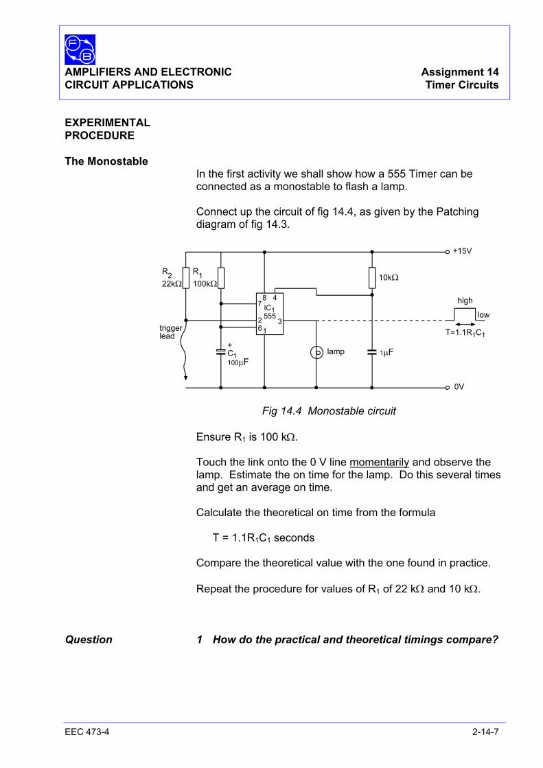
AMPLIFIERS AND ELECTRONIC Assignment 14 CIRCUIT APPLICATIONS Timer Circuits
EEC 473-4 2-14-7
EXPERIMENTAL PROCEDURE The Monostable In the first activity we shall show how a 555 Timer can be connected as a monostable to flash a lamp. Connect up the circuit of fig 14.4, as given by the Patching diagram of fig 14.3.
Fig 14.4 Monostable circuit Ensure R1 is 100 kΩ. Touch the link onto the 0 V line momentarily and observe the lamp. Estimate the on time for the lamp. Do this several times and get an average on time. Calculate the theoretical on time from the formula T = 1.1R1C1 seconds Compare the theoretical value with the one found in practice. Repeat the procedure for values of R1 of 22 kΩ and 10 kΩ. Question 1 How do the practical and theoretical timings compare?

AMPLIFIERS AND ELECTRONIC Assignment 14 CIRCUIT APPLICATIONS Timer Circuits
EEC 473-4 2-14-8
Notes

A
MPL
IFIE
RS
AN
D E
LEC
TRO
NIC
A
ssig
nmen
t 14
CIR
CU
IT A
PPLI
CA
TIO
NS
Tim
er C
ircui
ts
EE
C 4
73-4
2-
14-9
N
otes
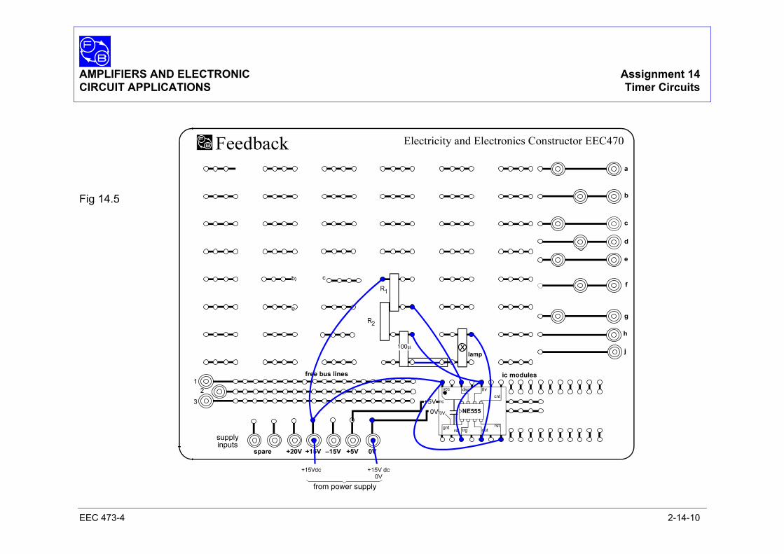
AMPLIFIERS AND ELECTRONIC Assignment 14 CIRCUIT APPLICATIONS Timer Circuits
EEC 473-4 2-14-10
Fig 14.5
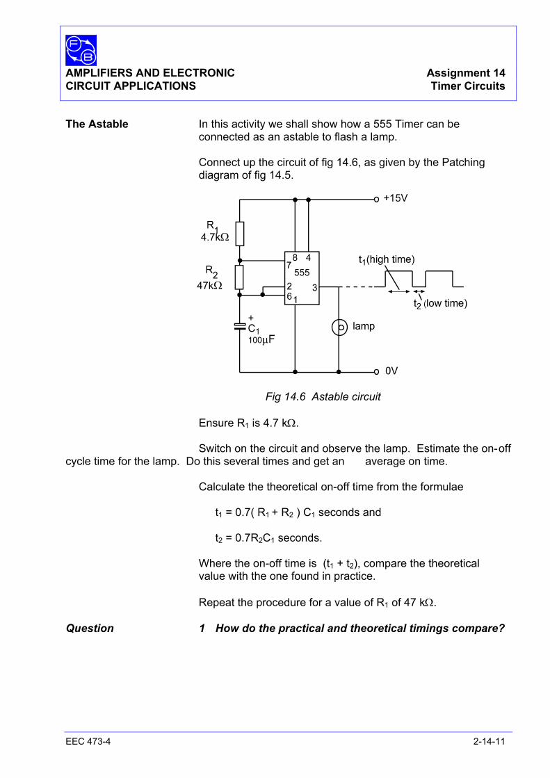
AMPLIFIERS AND ELECTRONIC Assignment 14 CIRCUIT APPLICATIONS Timer Circuits
EEC 473-4 2-14-11
The Astable In this activity we shall show how a 555 Timer can be connected as an astable to flash a lamp. Connect up the circuit of fig 14.6, as given by the Patching diagram of fig 14.5.
Fig 14.6 Astable circuit Ensure R1 is 4.7 kΩ. Switch on the circuit and observe the lamp. Estimate the on- off cycle time for the lamp. Do this several times and get an average on time. Calculate the theoretical on-off time from the formulae t1 = 0.7( R1 + R2 ) C1 seconds and t2 = 0.7R2C1 seconds. Where the on-off time is (t1 + t2), compare the theoretical value with the one found in practice. Repeat the procedure for a value of R1 of 47 kΩ. Question 1 How do the practical and theoretical timings compare?
AMPLIFIERS AND ELECTRONIC Assignment 14 CIRCUIT APPLICATIONS Timer Circuits
EEC 473-4 2-14-12
Notes

A
MPL
IFIE
RS
AN
D E
LEC
TRO
NIC
A
ssig
nmen
t 14
CIR
CU
IT A
PPLI
CA
TIO
NS
Tim
er C
ircui
ts
EE
C 4
73-4
2-
14-1
3
N
otes
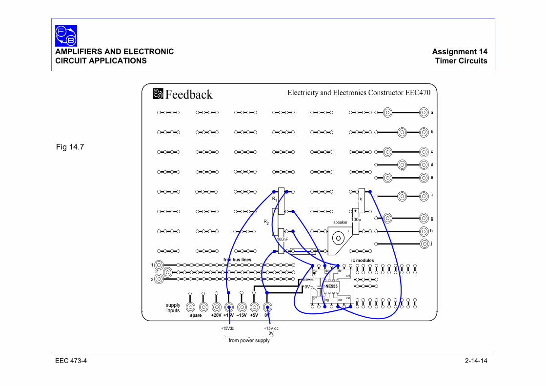
AMPLIFIERS AND ELECTRONIC Assignment 14 CIRCUIT APPLICATIONS Timer Circuits
EEC 473-4 2-14-14
Fig 14.7
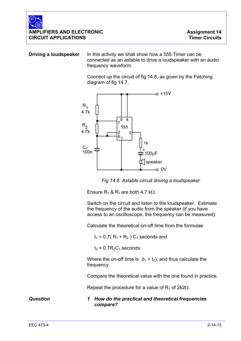
AMPLIFIERS AND ELECTRONIC Assignment 14 CIRCUIT APPLICATIONS Timer Circuits
EEC 473-4 2-14-15
Driving a loudspeaker In this activity we shall show how a 555 Timer can be connected as an astable to drive a loudspeaker with an audio frequency waveform. Connect up the circuit of fig 14.8, as given by the Patching diagram of fig 14.7.
Fig 14.8 Astable circuit driving a loudspeaker Ensure R1 & R1 are both 4.7 kΩ. Switch on the circuit and listen to the loudspeaker. Estimate the frequency of the audio from the speaker (if you have access to an oscilloscope, the frequency can be measured). Calculate the theoretical on-off time from the formulae t1 = 0.7( R1 + R2 ) C1 seconds and t2 = 0.7R2C1 seconds. Where the on-off time is (t1 + t2), and thus calculate the frequency. Compare the theoretical value with the one found in practice. Repeat the procedure for a value of R1 of 2k2Ω. Question 1 How do the practical and theoretical frequencies compare?

AMPLIFIERS AND ELECTRONIC Assignment 14 CIRCUIT APPLICATIONS Timer Circuits
EEC 473-4 2-14-16
Notes
Section 3 AMPLIFIERS AND ELECTRONIC CIRCUIT APPLICATIONS Control Applications
EEC 473-4 3-1
Control applications In this section we shall show some examples of simple control circuits that accept information from outside via a sensor and operate an output signal when the signal is within certain limits set by the circuit.
These simple circuits form the basis of many industrial process controllers; the output of which may take action to sound an alarm, correct an error, or even shutdown a system.

Section 3 AMPLIFIERS AND ELECTRONIC CIRCUIT APPLICATIONS Control Applications
EEC 473-4 3-2
Notes
Assignment 15 AMPLIFIERS AND ELECTRONIC CIRCUIT APPLICATIONS A Light Operated Alarm
EEC 473-4 3-15-1
EQUIPMENT REQUIRED Qty Apparatus 1 Electricity & Electronics Constructor EEC470 1 Circuit Applications Kit EEC473-4 1 Power supply unit +15 V dc regulated
(eg, Feedback Power Supply 92-445 or 92-100 Teknikit Console)
PREREQUISITES Assignment 6 KNOWLEDGE LEVEL Before considering this Assignment you should
• Know how an SCR operates
Assignment 15 AMPLIFIERS AND ELECTRONIC CIRCUIT APPLICATIONS A Light Operated Alarm
EEC 473-4 3-15-2
Notes

Ass
ignm
ent 1
5 A
MPL
IFIE
RS
AN
D E
LEC
TRO
NIC
CIR
CU
IT A
PPLI
CA
TIO
NS
A L
ight
Ope
rate
d A
larm
E
EC
473
-4
3-15
-3
Not
es
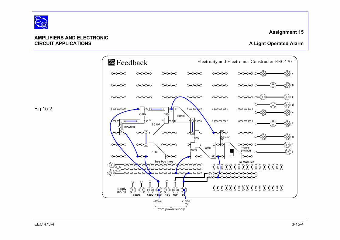
Assignment 15 AMPLIFIERS AND ELECTRONIC CIRCUIT APPLICATIONS A Light Operated Alarm
EEC 473-4 3-15-4
Fig 15-2
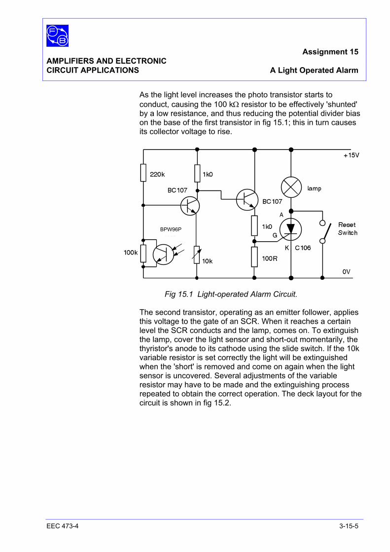
Assignment 15 AMPLIFIERS AND ELECTRONIC CIRCUIT APPLICATIONS A Light Operated Alarm
EEC 473-4 3-15-5
As the light level increases the photo transistor starts to conduct, causing the 100 kΩ resistor to be effectively 'shunted' by a low resistance, and thus reducing the potential divider bias on the base of the first transistor in fig 15.1; this in turn causes its collector voltage to rise.
Fig 15.1 Light-operated Alarm Circuit. The second transistor, operating as an emitter follower, applies
this voltage to the gate of an SCR. When it reaches a certain level the SCR conducts and the lamp, comes on. To extinguish the lamp, cover the light sensor and short-out momentarily, the thyristor's anode to its cathode using the slide switch. If the 10k variable resistor is set correctly the light will be extinguished when the 'short' is removed and come on again when the light sensor is uncovered. Several adjustments of the variable resistor may have to be made and the extinguishing process repeated to obtain the correct operation. The deck layout for the circuit is shown in fig 15.2.
BPW96P

Assignment 15 AMPLIFIERS AND ELECTRONIC CIRCUIT APPLICATIONS A Light Operated Alarm
EEC 473-4 3-15-6
Notes
Assignment 16 AMPLIFIERS AND ELECTRONIC CIRCUIT APPLICATIONS A Delay Circuit
EEC 473-4 3-16-1
EQUIPMENT REQUIRED Qty Apparatus 1 Electricity & Electronics Constructor EEC470 1 Circuit Assignments Kit EEC473-4 1 Power supply unit +15 V dc regulated
(eg, Feedback Power Supply 92-445 or 92-100 Teknikit Console)
PREREQUISITES Assignment 13 KNOWLEDGE LEVEL Before considering this Assignment you should :
• Know the operation of a Unijunction Transistor.
• Know how an SCR operates

Assignment 16 AMPLIFIERS AND ELECTRONIC CIRCUIT APPLICATIONS A Delay Circuit
EEC 473-4 3-16-2
Notes

Ass
ignm
ent 1
6 A
MPL
IFIE
RS
AN
D E
LEC
TRO
NIC
CIR
CU
IT A
PPLI
CA
TIO
NS
A D
elay
Circ
uit
EE
C 4
73-4
3-
16-3
Not
es
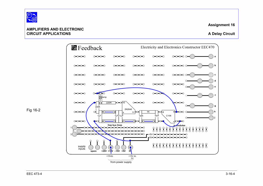
Assignment 16 AMPLIFIERS AND ELECTRONIC CIRCUIT APPLICATIONS A Delay Circuit
EEC 473-4 3-16-4
Fig 16-2
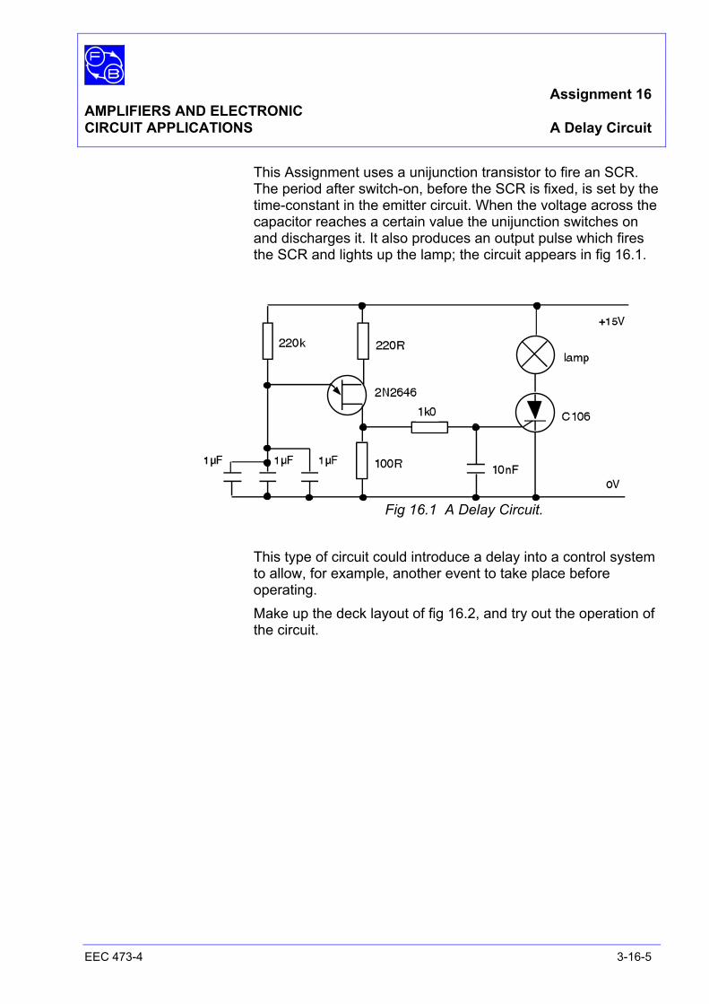
Assignment 16 AMPLIFIERS AND ELECTRONIC CIRCUIT APPLICATIONS A Delay Circuit
EEC 473-4 3-16-5
This Assignment uses a unijunction transistor to fire an SCR. The period after switch-on, before the SCR is fixed, is set by the time-constant in the emitter circuit. When the voltage across the capacitor reaches a certain value the unijunction switches on and discharges it. It also produces an output pulse which fires the SCR and lights up the lamp; the circuit appears in fig 16.1.
Fig 16.1 A Delay Circuit. This type of circuit could introduce a delay into a control system
to allow, for example, another event to take place before operating.
Make up the deck layout of fig 16.2, and try out the operation of the circuit.

Assignment 16 AMPLIFIERS AND ELECTRONIC CIRCUIT APPLICATIONS A Delay Circuit
EEC 473-4 3-16-6
Notes
Assignment 17 AMPLIFIERS AND ELECTRONIC CIRCUIT APPLICATIONS A Light Operated Flasher
EEC 473-4 3-17-1
EQUIPMENT REQUIRED Qty Apparatus 1 Electricity & Electronics Constructor EEC470 1 Circuit Applications Kit EEC473-4 1 Power supply unit +15 V dc regulated
(eg, Feedback Power Supply 92-445 or 92-100 Teknikit Console)
PREREQUISITES Assignment 16
KNOWLEDGE LEVEL Before considering this Assignment you should :
• Know the action of a commutating capacitor
Assignment 17 AMPLIFIERS AND ELECTRONIC CIRCUIT APPLICATIONS A Light Operated Flasher
EEC 473-4 3-17-2
Notes

Ass
ignm
ent 1
7 A
MPL
IFIE
RS
AN
D E
LEC
TRO
NIC
CIR
CU
IT A
PPLI
CA
TIO
NS
A L
ight
Ope
rate
d Fl
ashe
r E
EC
473
-4
3-17
-3
Not
es
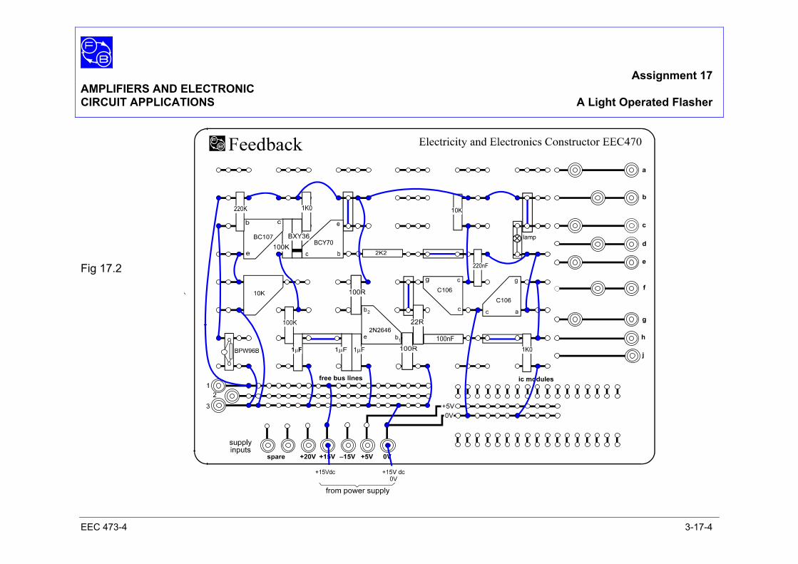
Assignment 17 AMPLIFIERS AND ELECTRONIC CIRCUIT APPLICATIONS A Light Operated Flasher
EEC 473-4 3-17-4
Fig 17.2
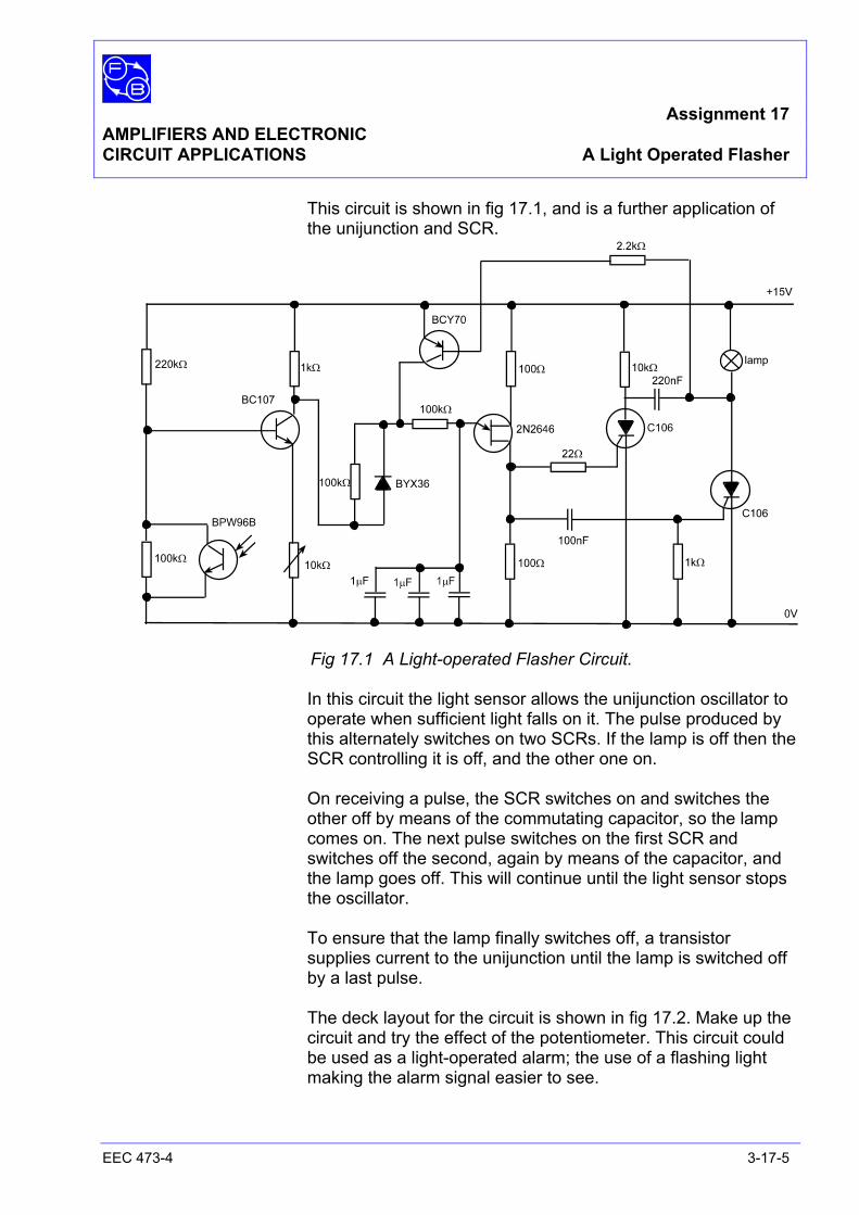
Assignment 17 AMPLIFIERS AND ELECTRONIC CIRCUIT APPLICATIONS A Light Operated Flasher
EEC 473-4 3-17-5
This circuit is shown in fig 17.1, and is a further application of the unijunction and SCR.
Fig 17.1 A Light-operated Flasher Circuit. In this circuit the light sensor allows the unijunction oscillator to
operate when sufficient light falls on it. The pulse produced by this alternately switches on two SCRs. If the lamp is off then the SCR controlling it is off, and the other one on.
On receiving a pulse, the SCR switches on and switches the
other off by means of the commutating capacitor, so the lamp comes on. The next pulse switches on the first SCR and switches off the second, again by means of the capacitor, and the lamp goes off. This will continue until the light sensor stops the oscillator.
To ensure that the lamp finally switches off, a transistor
supplies current to the unijunction until the lamp is switched off by a last pulse.
The deck layout for the circuit is shown in fig 17.2. Make up the
circuit and try the effect of the potentiometer. This circuit could be used as a light-operated alarm; the use of a flashing light making the alarm signal easier to see.
Assignment 17 AMPLIFIERS AND ELECTRONIC CIRCUIT APPLICATIONS A Light Operated Flasher
EEC 473-4 3-17-6
Notes
Assignment 18 AMPLIFIERS AND ELECTRONIC CIRCUIT APPLICATIONS A Temperature–Operated Switch
EEC 473-4 3-18-1
EQUIPMENT REQUIRED Qty Apparatus 1 Electricity & Electronics Constructor EEC470 1 Circuit Applications Kit EEC473-4 1 Power supply unit; +15 V dc regulated.
(eg, Feedback Power Supply 92-445 or 92-100 Teknikit Console)
PREREQUISITES Assignment 15
KNOWLEDGE LEVEL Before considering this Assignment you should :
• Know the operation of a Common Emitter amplifier
• Know how a Thermistor operates

Assignment 18 AMPLIFIERS AND ELECTRONIC CIRCUIT APPLICATIONS A Temperature–Operated Switch
EEC 473-4 3-18-2
Notes

Ass
ignm
ent 1
8 A
MPL
IFIE
RS
AN
D E
LEC
TRO
NIC
CIR
CU
IT A
PPLI
CA
TIO
NS
A T
empe
ratu
re–O
pera
ted
Switc
h E
EC
473
-4
3-18
-3
Not
es
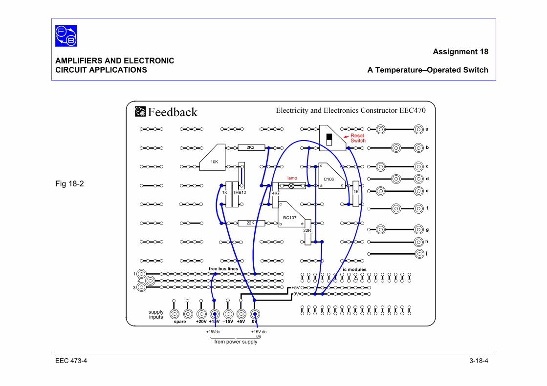
Assignment 18 AMPLIFIERS AND ELECTRONIC CIRCUIT APPLICATIONS A Temperature–Operated Switch
EEC 473-4 3-18-4
Fig 18-2
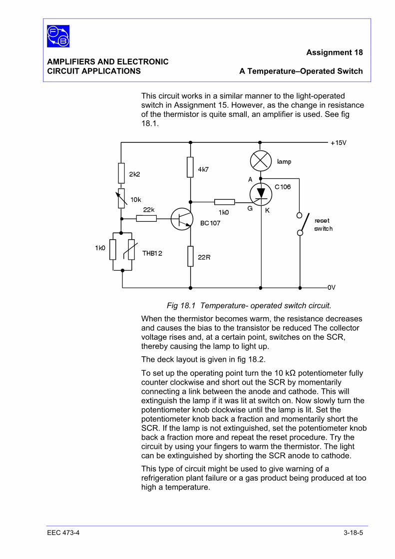
Assignment 18 AMPLIFIERS AND ELECTRONIC CIRCUIT APPLICATIONS A Temperature–Operated Switch
EEC 473-4 3-18-5
This circuit works in a similar manner to the light-operated switch in Assignment 15. However, as the change in resistance of the thermistor is quite small, an amplifier is used. See fig 18.1.
Fig 18.1 Temperature- operated switch circuit. When the thermistor becomes warm, the resistance decreases
and causes the bias to the transistor be reduced The collector voltage rises and, at a certain point, switches on the SCR, thereby causing the lamp to light up.
The deck layout is given in fig 18.2.
To set up the operating point turn the 10 kΩ potentiometer fully counter clockwise and short out the SCR by momentarily connecting a link between the anode and cathode. This will extinguish the lamp if it was lit at switch on. Now slowly turn the potentiometer knob clockwise until the lamp is lit. Set the potentiometer knob back a fraction and momentarily short the SCR. If the lamp is not extinguished, set the potentiometer knob back a fraction more and repeat the reset procedure. Try the circuit by using your fingers to warm the thermistor. The light can be extinguished by shorting the SCR anode to cathode.
This type of circuit might be used to give warning of a refrigeration plant failure or a gas product being produced at too high a temperature.
Assignment 18 AMPLIFIERS AND ELECTRONIC CIRCUIT APPLICATIONS A Temperature–Operated Switch
EEC 473-4 3-18-6
Notes
Assignment 19 AMPLIFIERS AND ELECTRONIC CIRCUIT APPLICATIONS The Schmitt Trigger
EEC 473-4 3-19-1
EQUIPMENT REQUIRED Qty Apparatus 1 Electricity & Electronics Constructor EEC470 1 Circuit Applications Kit EEC473-4
1 Power supply unit +15 V dc regulated (eg, Feedback Power Supply 92-445 or 92-100 Teknikit Console)
1 Function generator 6 V pk–pk triangle (eg, Feedback FG601)
1 2– Channel oscilloscope PREREQUISITES Assignment 10 KNOWLEDGE LEVEL Before considering this Assignment you should :
• Know how a voltage comparator circuit operates

Assignment 19 AMPLIFIERS AND ELECTRONIC CIRCUIT APPLICATIONS The Schmitt Trigger
EEC 473-4 3-19-2
Notes

Ass
ignm
ent 1
9 A
MPL
IFIE
RS
AN
D E
LEC
TRO
NIC
CIR
CU
IT A
PPLI
CA
TIO
NS
The
Schm
itt T
rigge
r E
EC
473
-4
3-19
-3
Not
es
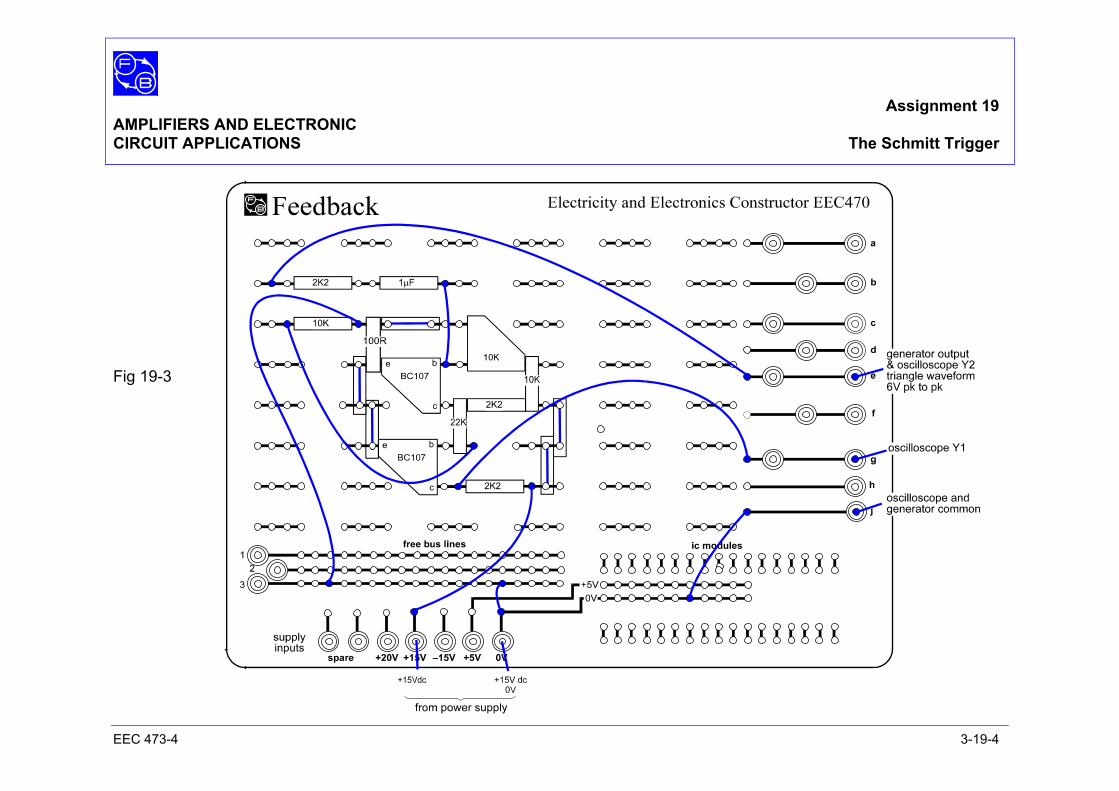
Assignment 19 AMPLIFIERS AND ELECTRONIC CIRCUIT APPLICATIONS The Schmitt Trigger
EEC 473-4 3-19-4
Fig 19-3
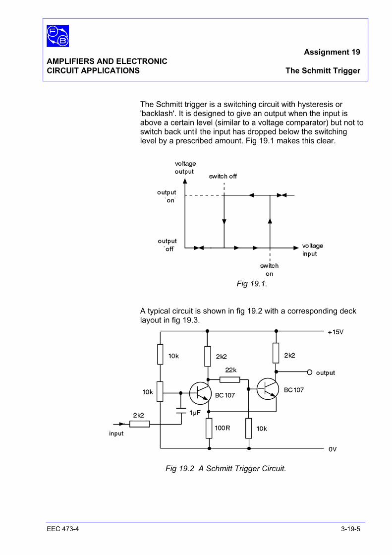
Assignment 19 AMPLIFIERS AND ELECTRONIC CIRCUIT APPLICATIONS The Schmitt Trigger
EEC 473-4 3-19-5
The Schmitt trigger is a switching circuit with hysteresis or
'backlash'. It is designed to give an output when the input is above a certain level (similar to a voltage comparator) but not to switch back until the input has dropped below the switching level by a prescribed amount. Fig 19.1 makes this clear.
Fig 19.1. A typical circuit is shown in fig 19.2 with a corresponding deck
layout in fig 19.3.
Fig 19.2 A Schmitt Trigger Circuit.
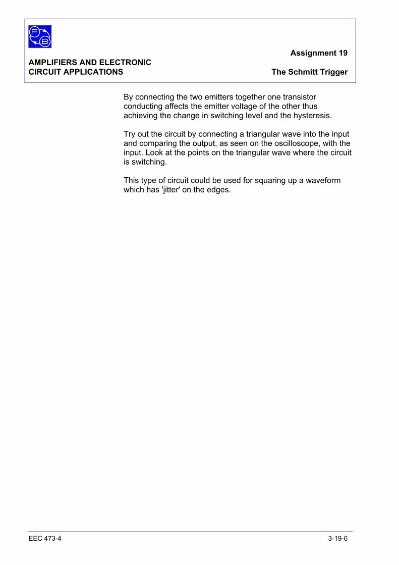
Assignment 19 AMPLIFIERS AND ELECTRONIC CIRCUIT APPLICATIONS The Schmitt Trigger
EEC 473-4 3-19-6
By connecting the two emitters together one transistor conducting affects the emitter voltage of the other thus achieving the change in switching level and the hysteresis.
Try out the circuit by connecting a triangular wave into the input
and comparing the output, as seen on the oscilloscope, with the input. Look at the points on the triangular wave where the circuit is switching.
This type of circuit could be used for squaring up a waveform
which has 'jitter' on the edges.
Assignment 20 AMPLIFIERS AND ELECTRONIC CIRCUIT APPLICATIONS A Voltage Regulator
EEC 473-4 3-20-1
EQUIPMENT REQUIRED Qty Apparatus
1 Electricity and Electronics Constructor EEC470
1 Circuit Applications Kit EEC473-4 1 Power supply unit; +15 V dc regulated
(eg, Feedback 92-445 or 92-100 Teknikit Console)
2 Multimeters or 1 Voltmeter 12 V dc and 1 Voltmeter 20 V dc PREREQUISITES Assignment 9 KNOWLEDGE LEVEL Before considering this Assignment you should :
• Know how a Zener Diode operates

Assignment 20 AMPLIFIERS AND ELECTRONIC CIRCUIT APPLICATIONS A Voltage Regulator
EEC 473-4 3-20-2
Notes

Ass
ignm
ent 2
0 A
MPL
IFIE
RS
AN
D E
LEC
TRO
NIC
CIR
CU
IT A
PPLI
CA
TIO
NS
A V
olta
ge R
egul
ator
E
EC
473
-4
3-20
-3
Not
es
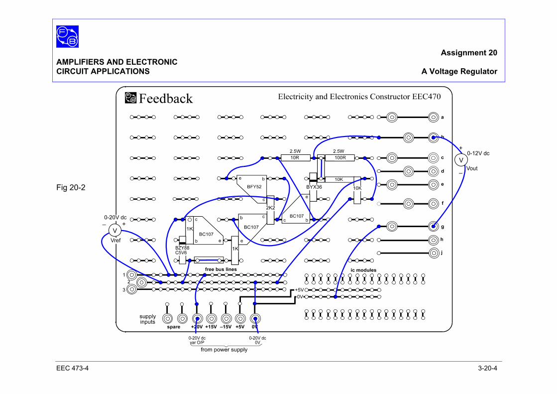
Assignment 20 AMPLIFIERS AND ELECTRONIC CIRCUIT APPLICATIONS A Voltage Regulator
EEC 473-4 3-20-4
Fig 20-2
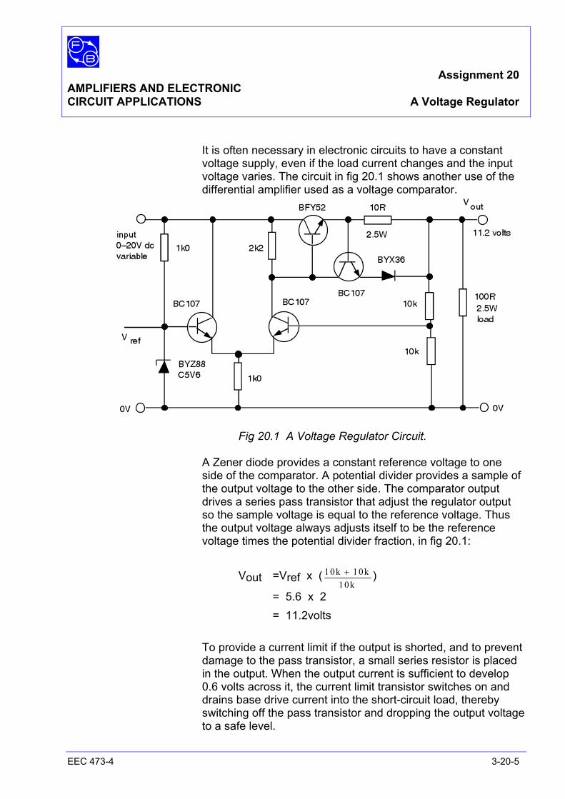
Assignment 20 AMPLIFIERS AND ELECTRONIC CIRCUIT APPLICATIONS A Voltage Regulator
EEC 473-4 3-20-5
It is often necessary in electronic circuits to have a constant
voltage supply, even if the load current changes and the input voltage varies. The circuit in fig 20.1 shows another use of the differential amplifier used as a voltage comparator.
Fig 20.1 A Voltage Regulator Circuit. A Zener diode provides a constant reference voltage to one
side of the comparator. A potential divider provides a sample of the output voltage to the other side. The comparator output drives a series pass transistor that adjust the regulator output so the sample voltage is equal to the reference voltage. Thus the output voltage always adjusts itself to be the reference voltage times the potential divider fraction, in fig 20.1:
Vout =Vref x ( 10 1010k kk
+ )
= 5.6 x 2 = 11.2volts To provide a current limit if the output is shorted, and to prevent
damage to the pass transistor, a small series resistor is placed in the output. When the output current is sufficient to develop 0.6 volts across it, the current limit transistor switches on and drains base drive current into the short-circuit load, thereby switching off the pass transistor and dropping the output voltage to a safe level.
Assignment 20 AMPLIFIERS AND ELECTRONIC CIRCUIT APPLICATIONS A Voltage Regulator
EEC 473-4 3-20-6
The deck layout for the circuit is shown in fig 20.2. Measure the output voltage with and without the 100 Ω load
resistor and vary the input voltage. Notice how the output voltage changes with the input voltage. This type of circuit is used extensively in regulated power supplies. By using integrated circuit versions of the circuit with higher gain amplifiers, very good regulation with few components can be obtained.
Section 4 AMPLIFIERS AND ELECTRONIC CIRCUIT APPLICATIONS Logic
EEC 473-4 4-1
Logic An important aspect of modern electronics involves the use of circuits, the output of which is all or nothing. These 'two-state' circuits can be used to perform a wide range of control functions from a simple alarm bell to a digital computer system capable of navigating man to the moon and back. Circuits that produce either zero volts output, called a binary zero, or a steady set voltage, called binary one, are called logic circuits.
The simplest type of logic circuits are 'gates'. These can have a number of inputs and one output, and produce an output when a certain combination of inputs is applied.
For example:
— One type of gate, called an AND gate, produces an output only when an input is present at all the points of inputs.
— Another produces an output when any one input is present; this is called an OR gate.
— A third type produces an output when there is a zero input but no output when there is a 'one' input, and this is called a NOT gate.
By combining a number of these gates together a logical control system can be developed. It might, for instance, work a lift and is called a 'combinational logic' system.
A second type of system involves the use of circuits that perform a sequential function whereby, a momentary input may change the output state which in turn remains so until the receipt of another signal. It might be a counting circuit that advances one count for each input cycle, and is called a 'sequential logic' system as its actions occur sequentially. Commonly both combinational and sequential logic are used together to form a powerful controller.
Due to the ease of dividing up the circuit into blocks, logic elements are normally supplied in integrated circuits, The logic designer therefore has no need to know what is inside the package as long as it performs the specified function.
In this section we shall make some of the simple logic functions from discrete components and thus show how they work. In the Feedback Logic Tutor LT345 kit, the use of integrated circuit logic elements is dealt with, and the mathematics used to simplify the design of logic systems described more fully. If is hoped however that this section will prevent you from thinking of logic elements purely as mysterious black boxes of integrated circuits.
Section 4 AMPLIFIERS AND ELECTRONIC CIRCUIT APPLICATIONS Logic
EEC 473-4 4-2
These logic functions can be implemented in several ways. Each combination of components used describes the 'family' to which the element belongs. There are six basic families:
1. Resistor-diode logic (RDL) This is the simplest system which contains no active
components and has limited use.
2. Resistor-transistor logic (RTL) This uses active components but has now been
superseded.
3. Diode-transistor logic (DTL) This also has been largely superseded.
4. Transistor-transistor logic (TTL) This is in common use for medium speed operation, but has
a high power consumption.
5. Complementary metal-oxide-silicon logic (CMOS) This uses pairs of field-effect transistors. It is slower that
TTL, but has a very low power consumption.
6. Emitter-coupled logic (ECL) This comprises groups of transistors (often pairs) with their
emitters joined together. It is the fastest form of logic generally available.
In the following Assignments some of these logic types will be
used to implement the basic logic functions.
Assignment 21 AMPLIFIERS AND ELECTRONIC CIRCUIT APPLICATIONS The RTL, RDL, DTL,TTL Gates
EEC 473-4 4-21-1
EQUIPMENT REQUIRED Qty Apparatus
1 Electricity & Electronics Constructor EEC470 1 Circuit Applications Kit EEC473-4 1 Power supply unit; +5 V dc regulated
(eg, Feedback Power Supply 92-445 or 92-100 Teknikit Console)
1 Multimeter or 1 Voltmeter 5 V dc PREREQUISITES Assignment 6 KNOWLEDGE LEVEL Before considering this Application you should :
• Know how a Junction Diode operates • Know how a Bipolar Transistor operates
Assignment 21 AMPLIFIERS AND ELECTRONIC CIRCUIT APPLICATIONS The RTL, RDL, DTL,TTL Gates
EEC 473-4 4-21-2
Notes

Ass
ignm
ent 2
1 A
MPL
IFIE
RS
AN
D E
LEC
TRO
NIC
CIR
CU
IT A
PPLI
CA
TIO
NS
The
RTL
, RD
L, D
TL,T
TL G
ates
E
EC
473
-4
4-21
-3
Not
es
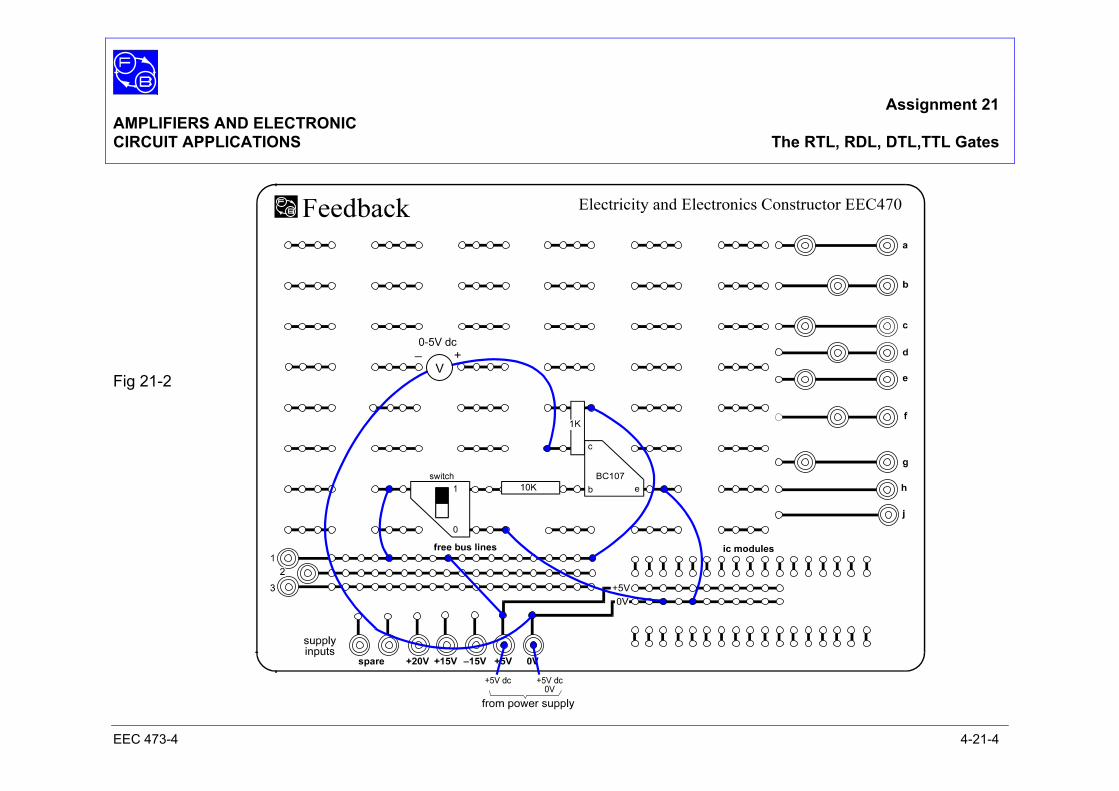
Assignment 21 AMPLIFIERS AND ELECTRONIC CIRCUIT APPLICATIONS The RTL, RDL, DTL,TTL Gates
EEC 473-4 4-21-4
Fig 21-2
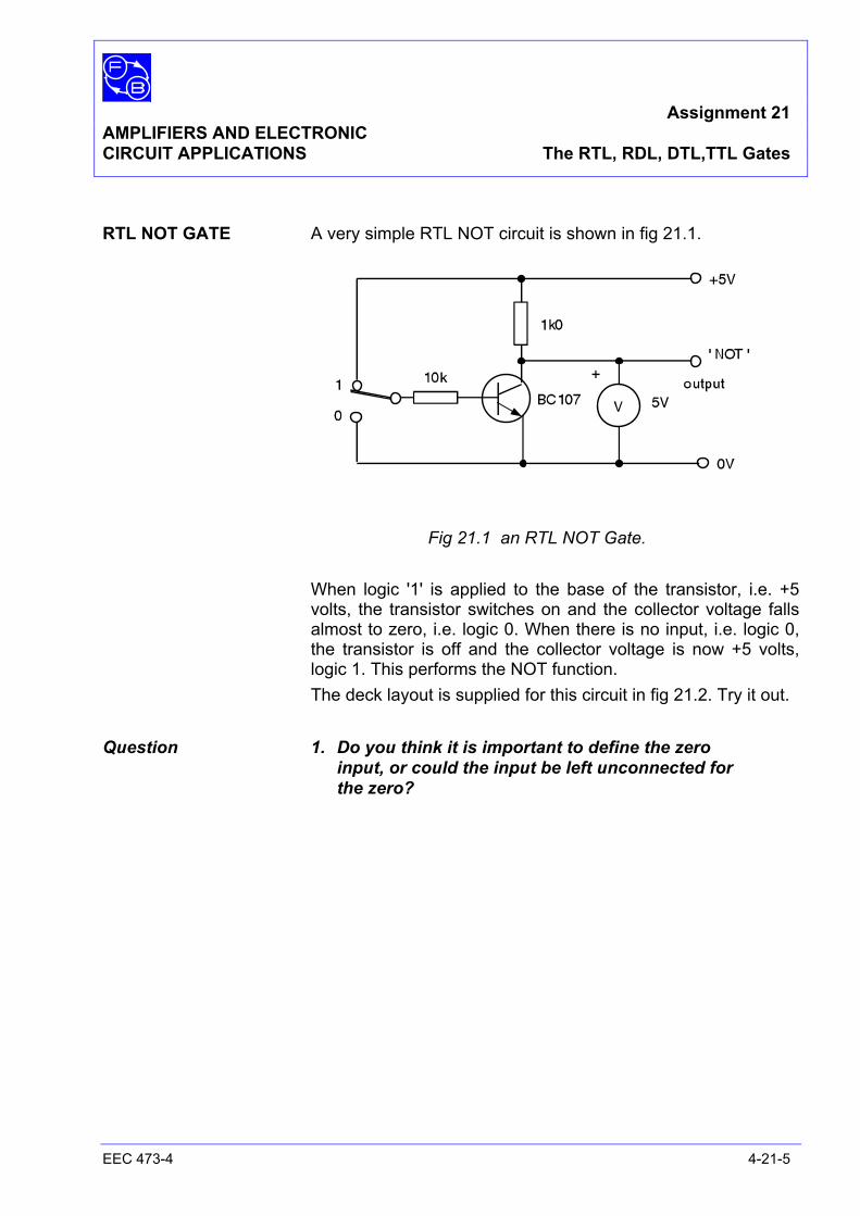
Assignment 21 AMPLIFIERS AND ELECTRONIC CIRCUIT APPLICATIONS The RTL, RDL, DTL,TTL Gates
EEC 473-4 4-21-5
RTL NOT GATE A very simple RTL NOT circuit is shown in fig 21.1.
Fig 21.1 an RTL NOT Gate. When logic '1' is applied to the base of the transistor, i.e. +5
volts, the transistor switches on and the collector voltage falls almost to zero, i.e. logic 0. When there is no input, i.e. logic 0, the transistor is off and the collector voltage is now +5 volts, logic 1. This performs the NOT function.
The deck layout is supplied for this circuit in fig 21.2. Try it out. Question 1. Do you think it is important to define the zero
input, or could the input be left unconnected for the zero?

Assignment 21 AMPLIFIERS AND ELECTRONIC CIRCUIT APPLICATIONS The RTL, RDL, DTL,TTL Gates
EEC 473-4 4-21-6
Notes

Ass
ignm
ent 2
1 A
MPL
IFIE
RS
AN
D E
LEC
TRO
NIC
CIR
CU
IT A
PPLI
CA
TIO
NS
The
RTL
, RD
L, D
TL,T
TL G
ates
E
EC
473
-4
4-21
-7
Not
es
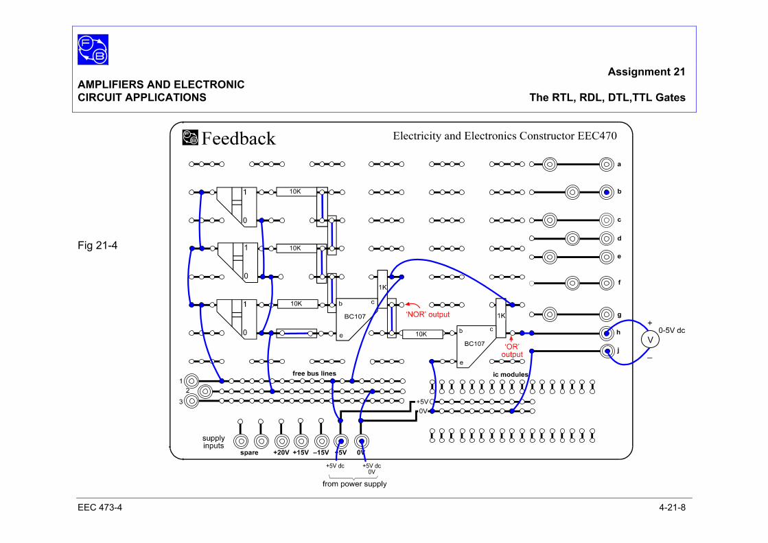
Assignment 21 AMPLIFIERS AND ELECTRONIC CIRCUIT APPLICATIONS The RTL, RDL, DTL,TTL Gates
EEC 473-4 4-21-8
Fig 21-4
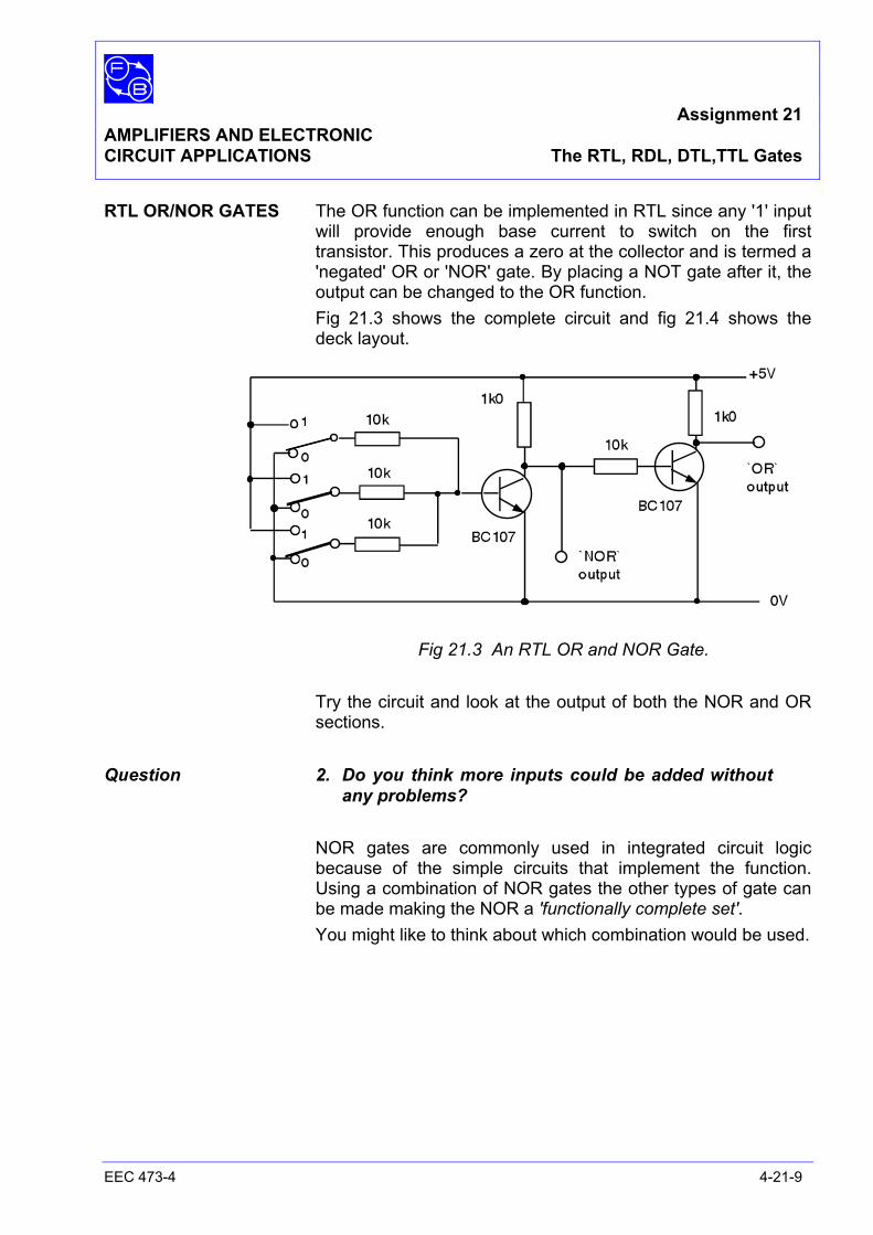
Assignment 21 AMPLIFIERS AND ELECTRONIC CIRCUIT APPLICATIONS The RTL, RDL, DTL,TTL Gates
EEC 473-4 4-21-9
RTL OR/NOR GATES The OR function can be implemented in RTL since any '1' input will provide enough base current to switch on the first transistor. This produces a zero at the collector and is termed a 'negated' OR or 'NOR' gate. By placing a NOT gate after it, the output can be changed to the OR function.
Fig 21.3 shows the complete circuit and fig 21.4 shows the deck layout.
Fig 21.3 An RTL OR and NOR Gate.
Try the circuit and look at the output of both the NOR and OR
sections. Question 2. Do you think more inputs could be added without
any problems? NOR gates are commonly used in integrated circuit logic
because of the simple circuits that implement the function. Using a combination of NOR gates the other types of gate can be made making the NOR a 'functionally complete set'.
You might like to think about which combination would be used.

Assignment 21 AMPLIFIERS AND ELECTRONIC CIRCUIT APPLICATIONS The RTL, RDL, DTL,TTL Gates
EEC 473-4 4-21-10
Notes

Ass
ignm
ent 2
1 A
MPL
IFIE
RS
AN
D E
LEC
TRO
NIC
CIR
CU
IT A
PPLI
CA
TIO
NS
The
RTL
, RD
L, D
TL,T
TL G
ates
E
EC
473
-4
4-21
-11
Not
es
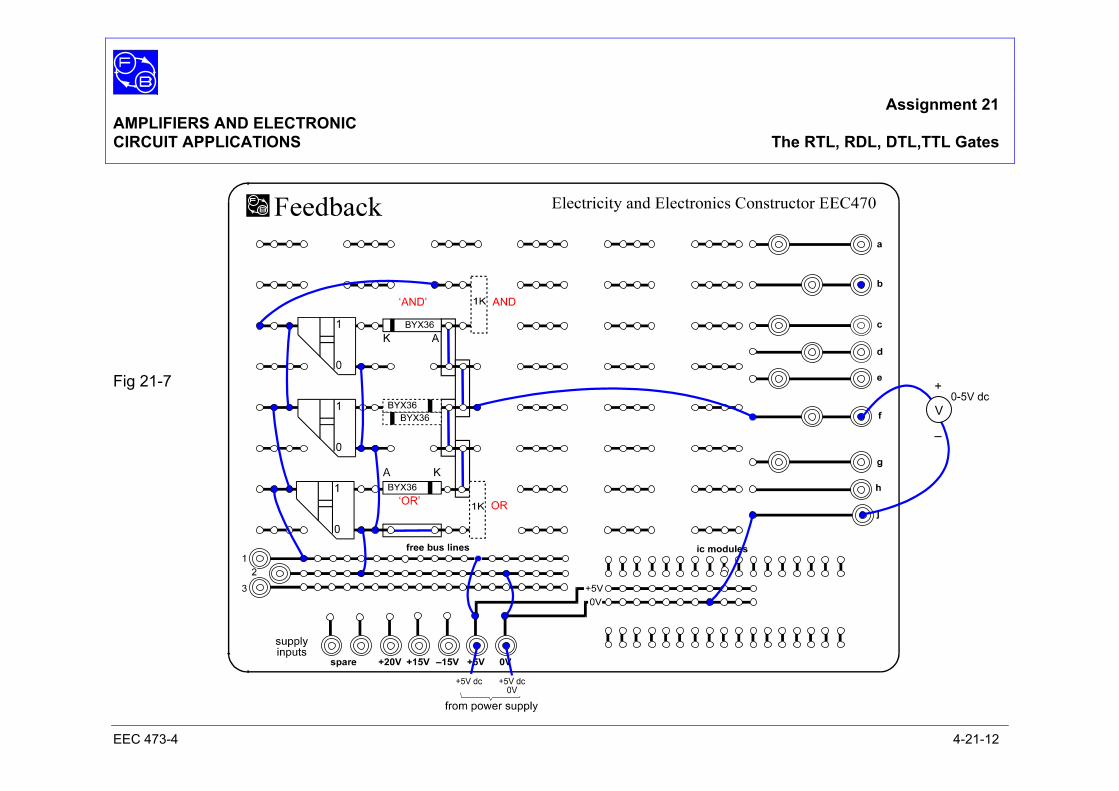
Assignment 21 AMPLIFIERS AND ELECTRONIC CIRCUIT APPLICATIONS The RTL, RDL, DTL,TTL Gates
EEC 473-4 4-21-12
Fig 21-7
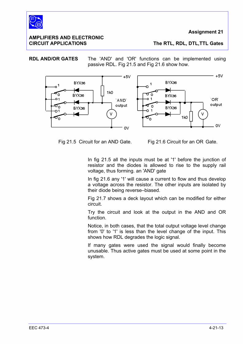
Assignment 21 AMPLIFIERS AND ELECTRONIC CIRCUIT APPLICATIONS The RTL, RDL, DTL,TTL Gates
EEC 473-4 4-21-13
RDL AND/OR GATES The 'AND' and 'OR' functions can be implemented using passive RDL. Fig 21.5 and Fig 21.6 show how.
Fig 21.5 Circuit for an AND Gate. Fig 21.6 Circuit for an OR Gate.
In fig 21.5 all the inputs must be at '1' before the junction of
resistor and the diodes is allowed to rise to the supply rail voltage, thus forming. an 'AND' gate
In fig 21.6 any '1' will cause a current to flow and thus develop a voltage across the resistor. The other inputs are isolated by their diode being reverse–biased.
Fig 21.7 shows a deck layout which can be modified for either circuit.
Try the circuit and look at the output in the AND and OR function.
Notice, in both cases, that the total output voltage level change from '0' to '1' is less than the level change of the input. This shows how RDL degrades the logic signal.
If many gates were used the signal would finally become unusable. Thus active gates must be used at some point in the system.

Assignment 21 AMPLIFIERS AND ELECTRONIC CIRCUIT APPLICATIONS The RTL, RDL, DTL,TTL Gates
EEC 473-4 4-21-14
Notes
Ass
ignm
ent 2
1 A
MPL
IFIE
RS
AN
D E
LEC
TRO
NIC
CIR
CU
IT A
PPLI
CA
TIO
NS
The
RTL
, RD
L, D
TL,T
TL G
ates
E
EC
473
-4
4-21
-15
Not
es
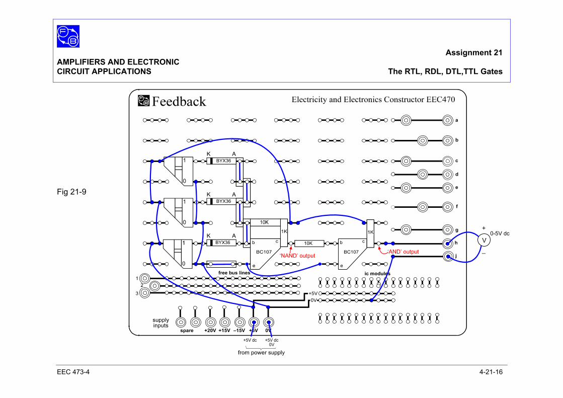
Assignment 21 AMPLIFIERS AND ELECTRONIC CIRCUIT APPLICATIONS The RTL, RDL, DTL,TTL Gates
EEC 473-4 4-21-16
Fig 21-9
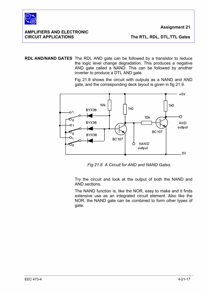
Assignment 21 AMPLIFIERS AND ELECTRONIC CIRCUIT APPLICATIONS The RTL, RDL, DTL,TTL Gates
EEC 473-4 4-21-17
RDL AND/NAND GATES The RDL AND gate can be followed by a transistor to reduce the logic level change degradation. This produces a negative AND gate called a NAND. This can be followed by another inverter to produce a DTL AND gate.
Fig 21.8 shows the circuit with outputs as a NAND and AND gate, and the corresponding deck layout is given in fig 21.9.
Fig 21.8 A Circuit for AND and NAND Gates.
Try the circuit and look at the output of both the NAND and AND sections.
The NAND function is, like the NOR, easy to make and it finds extensive use as an integrated circuit element. Also like the NOR, the NAND gate can be combined to form other types of gate.
Assignment 21 AMPLIFIERS AND ELECTRONIC CIRCUIT APPLICATIONS The RTL, RDL, DTL,TTL Gates
EEC 473-4 4-21-18
Notes

Ass
ignm
ent 2
1 A
MPL
IFIE
RS
AN
D E
LEC
TRO
NIC
CIR
CU
IT A
PPLI
CA
TIO
NS
The
RTL
, RD
L, D
TL,T
TL G
ates
E
EC
473
-4
4-21
-19
Not
es
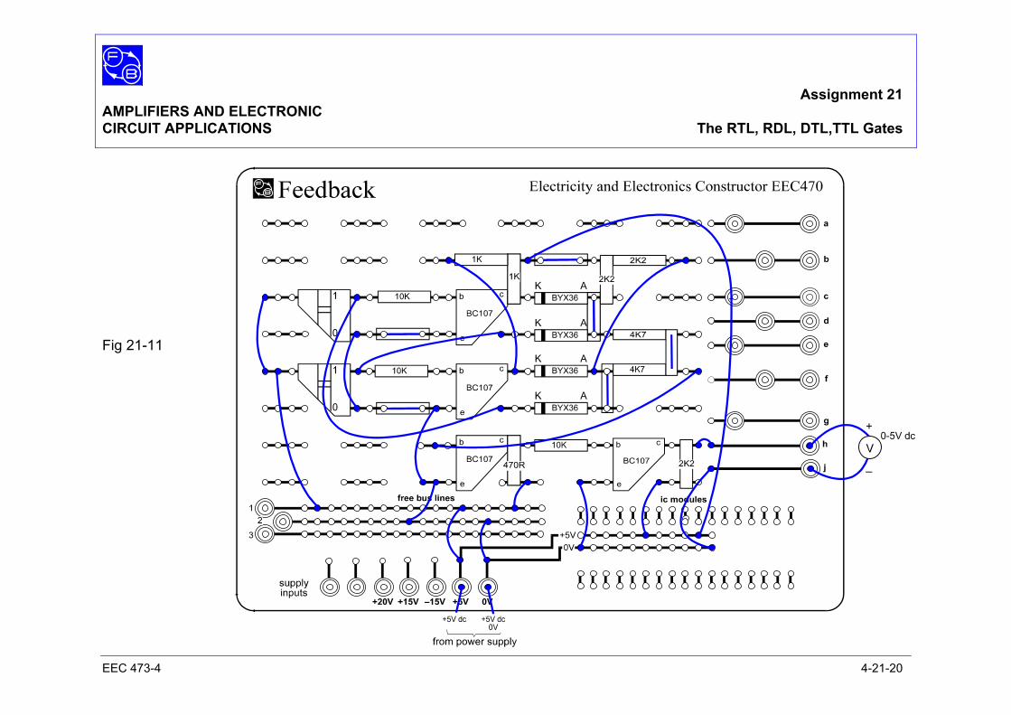
Assignment 21 AMPLIFIERS AND ELECTRONIC CIRCUIT APPLICATIONS The RTL, RDL, DTL,TTL Gates
EEC 473-4 4-21-20
Fig 21-11
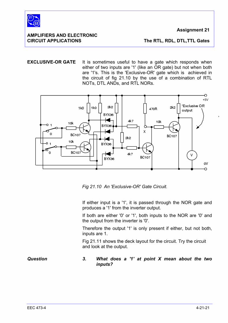
Assignment 21 AMPLIFIERS AND ELECTRONIC CIRCUIT APPLICATIONS The RTL, RDL, DTL,TTL Gates
EEC 473-4 4-21-21
EXCLUSIVE-OR GATE It is sometimes useful to have a gate which responds when
either of two inputs are '1' (like an OR gate) but not when both are '1's. This is the 'Exclusive-OR' gate which is achieved in the circuit of fig 21.10 by the use of a combination of RTL NOTs, DTL ANDs, and RTL NORs.
Fig 21.10 An 'Exclusive-OR' Gate Circuit.
If either input is a '1', it is passed through the NOR gate and produces a '1' from the inverter output.
If both are either '0' or '1', both inputs to the NOR are '0' and the output from the inverter is '0'.
Therefore the output '1' is only present if either, but not both, inputs are 1.
Fig 21.11 shows the deck layout for the circuit. Try the circuit and look at the output.
Question 3. What does a '1' at point X mean about the two
inputs?
+5V

Assignment 21 AMPLIFIERS AND ELECTRONIC CIRCUIT APPLICATIONS The RTL, RDL, DTL,TTL Gates
EEC 473-4 4-21-22
Notes

Ass
ignm
ent 2
1 A
MPL
IFIE
RS
AN
D E
LEC
TRO
NIC
CIR
CU
IT A
PPLI
CA
TIO
NS
The
RTL
, RD
L, D
TL,T
TL G
ates
E
EC
473
-4
4-21
-23
Not
es
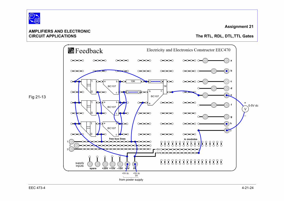
Assignment 21 AMPLIFIERS AND ELECTRONIC CIRCUIT APPLICATIONS The RTL, RDL, DTL,TTL Gates
EEC 473-4 4-21-24
Fig 21-13
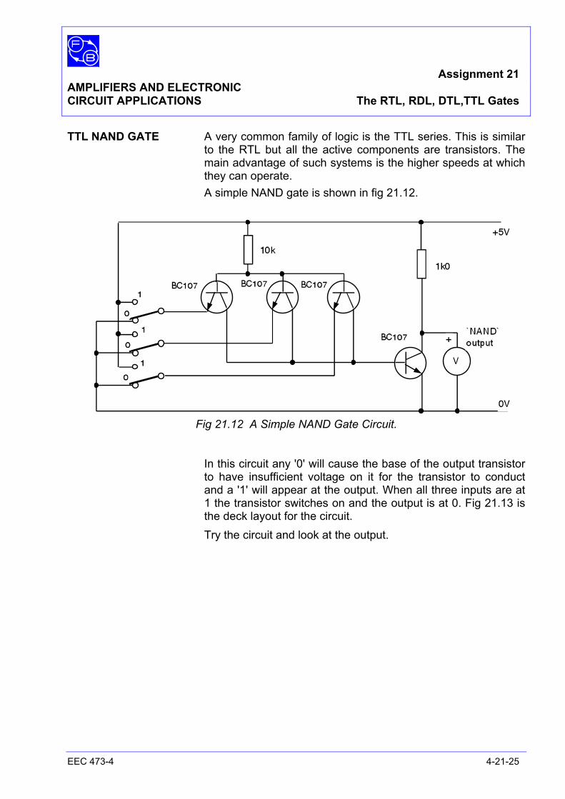
Assignment 21 AMPLIFIERS AND ELECTRONIC CIRCUIT APPLICATIONS The RTL, RDL, DTL,TTL Gates
EEC 473-4 4-21-25
TTL NAND GATE A very common family of logic is the TTL series. This is similar to the RTL but all the active components are transistors. The main advantage of such systems is the higher speeds at which they can operate.
A simple NAND gate is shown in fig 21.12.
Fig 21.12 A Simple NAND Gate Circuit.
In this circuit any '0' will cause the base of the output transistor to have insufficient voltage on it for the transistor to conduct and a '1' will appear at the output. When all three inputs are at 1 the transistor switches on and the output is at 0. Fig 21.13 is the deck layout for the circuit.
Try the circuit and look at the output.

Assignment 21 AMPLIFIERS AND ELECTRONIC CIRCUIT APPLICATIONS The RTL, RDL, DTL,TTL Gates
EEC 473-4 4-21-26
Notes
Assignment 21 AMPLIFIERS AND ELECTRONIC CIRCUIT APPLICATIONS Answers
EEC 473-4 4-21-27
Answer to questions in Assignment 21 1. An input which is left open-circuit can be either '0' or '1'
depending on leakage and interference. The gate can therefore cause mal-operation of the circuit.
2. If more input resistors are added, the value of each resistor has to be reduced to provide enough base current from one input, with the rest by-passing current to ground in the zero condition. The system cannot be expanded very far before it ceases to function.
3. Point 'x' is a '1' when both inputs have the same logic value on them; i.e. they are both'1's or both zeros. This is an "EQUIVALENCE GATE'.

Assignment 21 AMPLIFIERS AND ELECTRONIC CIRCUIT APPLICATIONS Answers
EEC 473-4 4-21-28
Notes
Assignment 22 AMPLIFIERS AND ELECTRONIC CIRCUIT APPLICATIONS The Flip–Flops
EEC 473-4 4-22-1
EQUIPMENT REQUIRED Qty Apparatus
1 Electricity & Electronics Constructor EEC470 1 Circuit Applications Kit EEC474 1 Power supply unit; +5 V dc. regulated
(eg, Feedback Power Supply 92-445 or 92-100 Teknikit Console)
1 Multimeter or 1 Voltmeter 5 V dc 1 Function Generator, Squarewave,
5 V pk-pk, 1 Hz 1 2-Channel Oscilloscope PREREQUISITES Assignment 21 KNOWLEDGE LEVEL See prerequisites

Assignment 22 AMPLIFIERS AND ELECTRONIC CIRCUIT APPLICATIONS The Flip–Flops
EEC 473-4 4-22-2
Notes

Ass
ignm
ent 2
2 A
MPL
IFIE
RS
AN
D E
LEC
TRO
NIC
CIR
CU
IT A
PPLI
CA
TIO
NS
The
Flip
–Flo
ps
EE
C 4
73-4
4-
22-3
Not
es
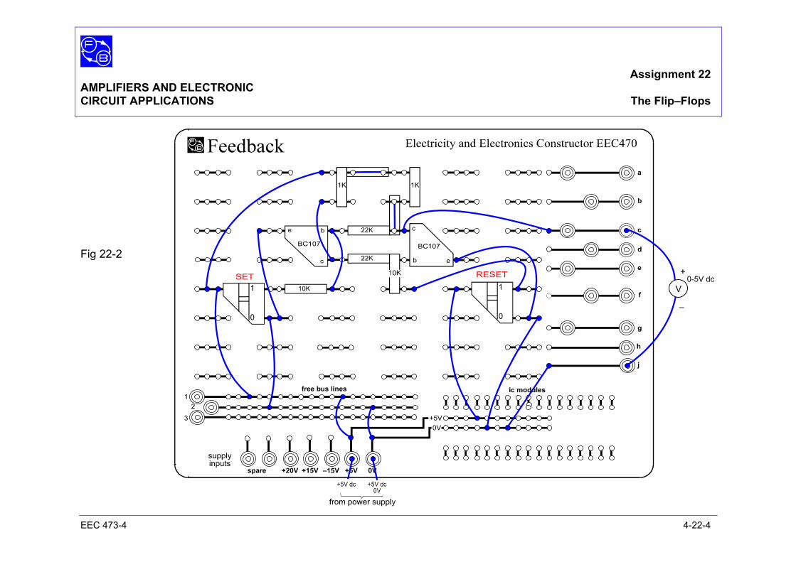
Assignment 22 AMPLIFIERS AND ELECTRONIC CIRCUIT APPLICATIONS The Flip–Flops
EEC 473-4 4-22-4
Fig 22-2
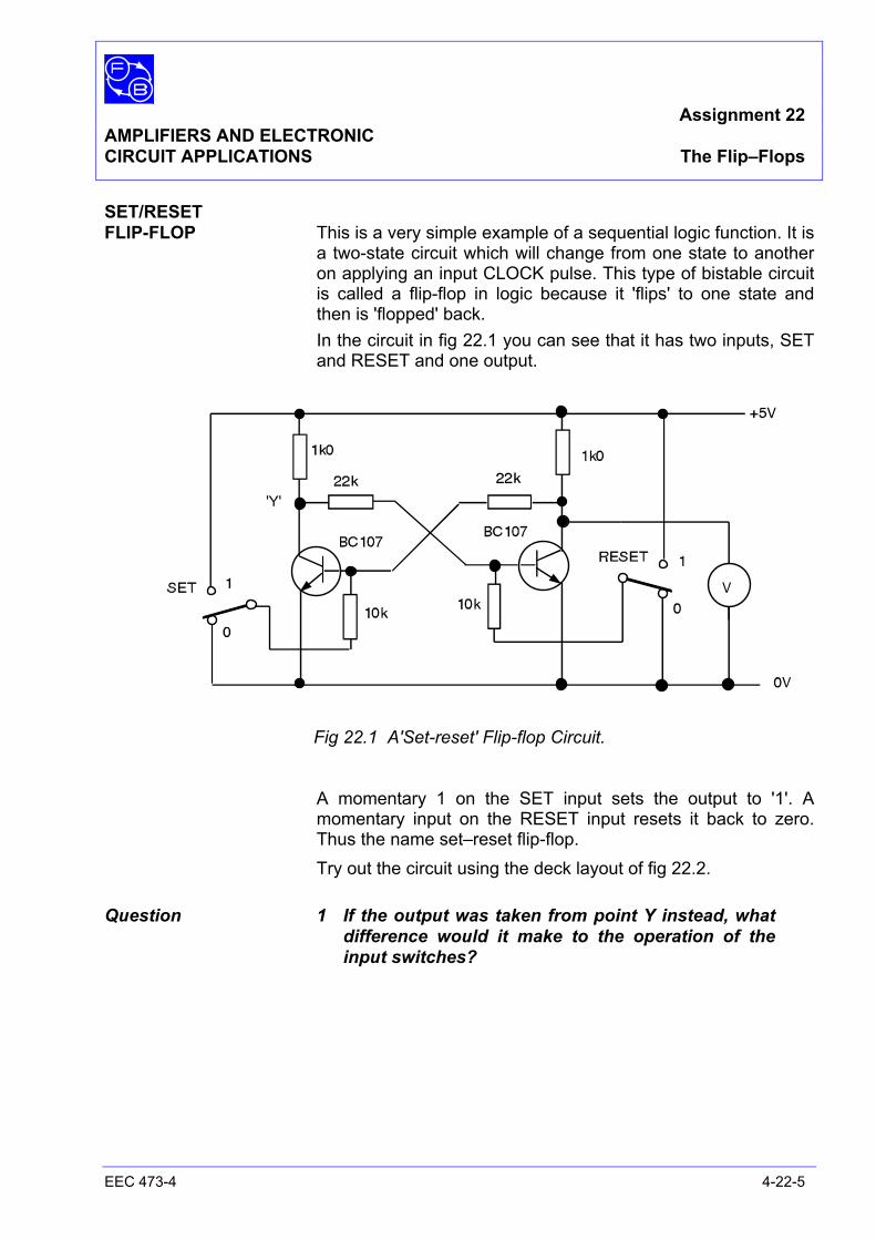
Assignment 22 AMPLIFIERS AND ELECTRONIC CIRCUIT APPLICATIONS The Flip–Flops
EEC 473-4 4-22-5
SET/RESET FLIP-FLOP This is a very simple example of a sequential logic function. It is
a two-state circuit which will change from one state to another on applying an input CLOCK pulse. This type of bistable circuit is called a flip-flop in logic because it 'flips' to one state and then is 'flopped' back.
In the circuit in fig 22.1 you can see that it has two inputs, SET and RESET and one output.
Fig 22.1 A'Set-reset' Flip-flop Circuit.
A momentary 1 on the SET input sets the output to '1'. A momentary input on the RESET input resets it back to zero. Thus the name set–reset flip-flop.
Try out the circuit using the deck layout of fig 22.2. Question 1 If the output was taken from point Y instead, what
difference would it make to the operation of the input switches?

Assignment 22 AMPLIFIERS AND ELECTRONIC CIRCUIT APPLICATIONS The Flip–Flops
EEC 473-4 4-22-6
Notes

Ass
ignm
ent 2
2 A
MPL
IFIE
RS
AN
D E
LEC
TRO
NIC
CIR
CU
IT A
PPLI
CA
TIO
NS
The
Flip
–Flo
ps
EE
C 4
73-4
4-
22-7
Not
es
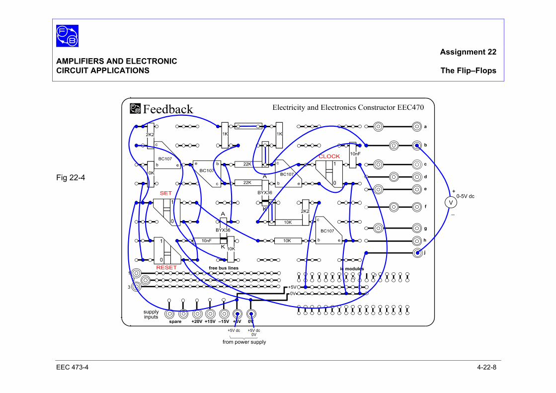
Assignment 22 AMPLIFIERS AND ELECTRONIC CIRCUIT APPLICATIONS The Flip–Flops
EEC 473-4 4-22-8
Fig 22-4
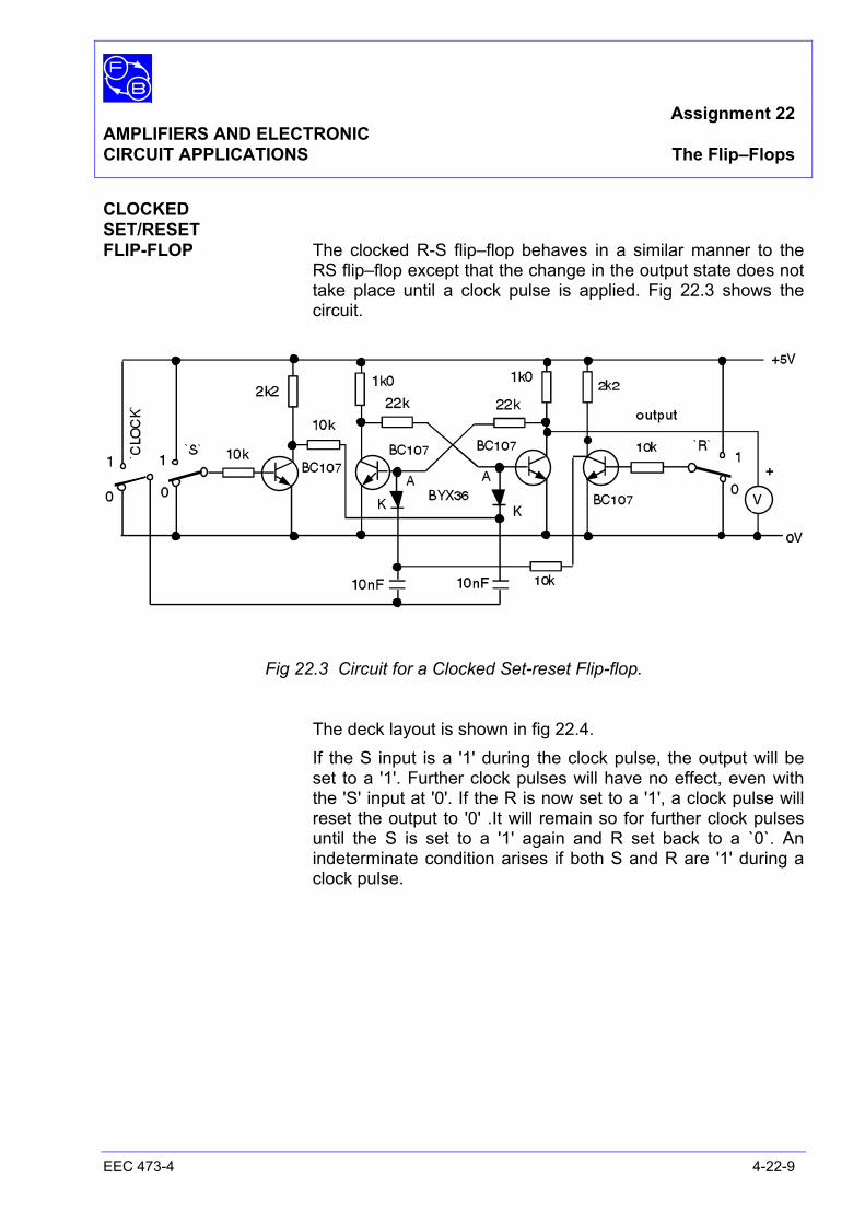
Assignment 22 AMPLIFIERS AND ELECTRONIC CIRCUIT APPLICATIONS The Flip–Flops
EEC 473-4 4-22-9
CLOCKED SET/RESET FLIP-FLOP The clocked R-S flip–flop behaves in a similar manner to the
RS flip–flop except that the change in the output state does not take place until a clock pulse is applied. Fig 22.3 shows the circuit.
Fig 22.3 Circuit for a Clocked Set-reset Flip-flop.
The deck layout is shown in fig 22.4. If the S input is a '1' during the clock pulse, the output will be
set to a '1'. Further clock pulses will have no effect, even with the 'S' input at '0'. If the R is now set to a '1', a clock pulse will reset the output to '0' .It will remain so for further clock pulses until the S is set to a '1' again and R set back to a `0`. An indeterminate condition arises if both S and R are '1' during a clock pulse.

Assignment 22 AMPLIFIERS AND ELECTRONIC CIRCUIT APPLICATIONS The Flip–Flops
EEC 473-4 4-22-10
Notes

Ass
ignm
ent 2
2 A
MPL
IFIE
RS
AN
D E
LEC
TRO
NIC
CIR
CU
IT A
PPLI
CA
TIO
NS
The
Flip
–Flo
ps
EE
C 4
73-4
4-
22-1
1
Not
es
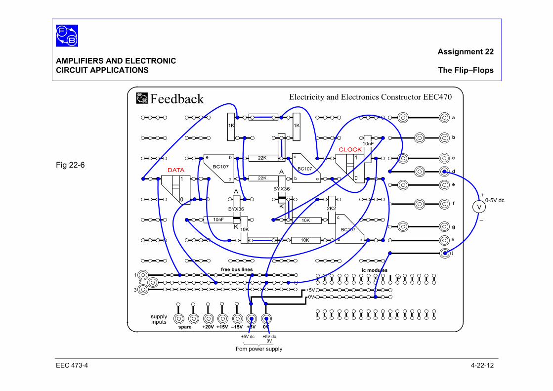
Assignment 22 AMPLIFIERS AND ELECTRONIC CIRCUIT APPLICATIONS The Flip–Flops
EEC 473-4 4-22-12
Fig 22-6
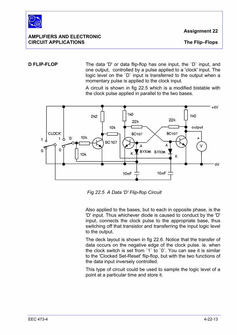
Assignment 22 AMPLIFIERS AND ELECTRONIC CIRCUIT APPLICATIONS The Flip–Flops
EEC 473-4 4-22-13
D FLIP-FLOP The data 'D' or data flip-flop has one input, the `D` input, and
one output, controlled by a pulse applied to a 'clock' input. The logic level on the `D` input is transferred to the output when a momentary pulse is applied to the clock input.
A circuit is shown in fig 22.5 which is a modified bistable with the clock pulse applied in parallel to the two bases.
Fig 22.5 A Data 'D' Flip-flop Circuit
Also applied to the bases, but to each in opposite phase, is the
'D' input. Thus whichever diode is caused to conduct by the 'D' input, connects the clock pulse to the appropriate base, thus switching off that transistor and transferring the input logic level to the output.
The deck layout is shown in fig 22.6. Notice that the transfer of data occurs on the negative edge of the clock pulse. ie. when the clock switch is set from `1` to `0`. You can see it is similar to the 'Clocked Set-Reset' flip-flop, but with the two functions of the data input inversely controlled.
This type of circuit could be used to sample the logic level of a point at a particular time and store it.

Assignment 22 AMPLIFIERS AND ELECTRONIC CIRCUIT APPLICATIONS The Flip–Flops
EEC 473-4 4-22-14
Notes

Ass
ignm
ent 2
2 A
MPL
IFIE
RS
AN
D E
LEC
TRO
NIC
CIR
CU
IT A
PPLI
CA
TIO
NS
The
Flip
–Flo
ps
EE
C 4
73-4
4-
22-1
5
Not
es
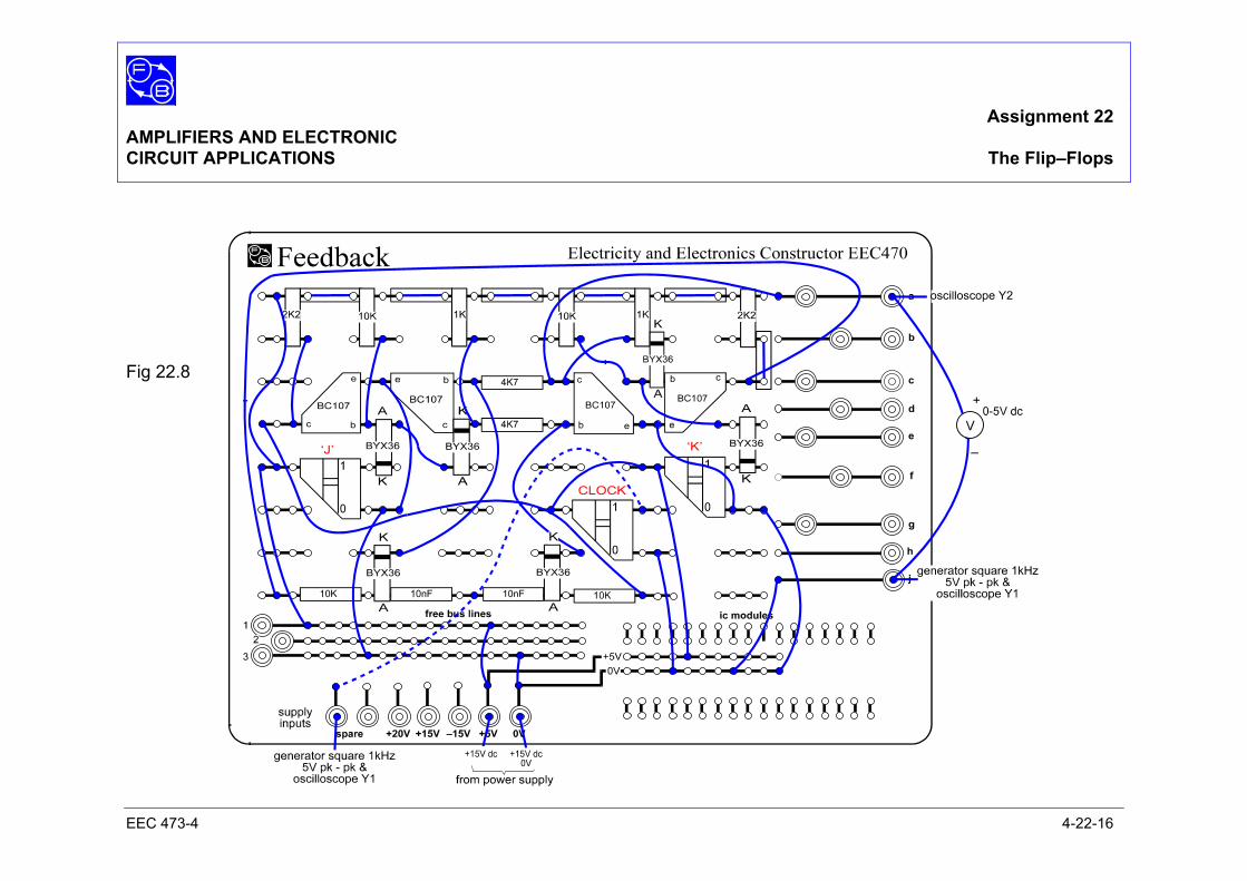
Assignment 22 AMPLIFIERS AND ELECTRONIC CIRCUIT APPLICATIONS The Flip–Flops
EEC 473-4 4-22-16
Fig 22.8
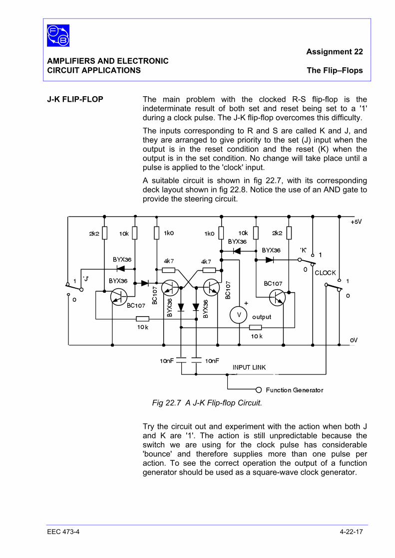
Assignment 22 AMPLIFIERS AND ELECTRONIC CIRCUIT APPLICATIONS The Flip–Flops
EEC 473-4 4-22-17
J-K FLIP-FLOP The main problem with the clocked R-S flip-flop is the indeterminate result of both set and reset being set to a '1' during a clock pulse. The J-K flip-flop overcomes this difficulty.
The inputs corresponding to R and S are called K and J, and they are arranged to give priority to the set (J) input when the output is in the reset condition and the reset (K) when the output is in the set condition. No change will take place until a pulse is applied to the 'clock' input.
A suitable circuit is shown in fig 22.7, with its corresponding deck layout shown in fig 22.8. Notice the use of an AND gate to provide the steering circuit.
Fig 22.7 A J-K Flip-flop Circuit.
Try the circuit out and experiment with the action when both J
and K are '1'. The action is still unpredictable because the switch we are using for the clock pulse has considerable 'bounce' and therefore supplies more than one pulse per action. To see the correct operation the output of a function generator should be used as a square-wave clock generator.
Assignment 22 AMPLIFIERS AND ELECTRONIC CIRCUIT APPLICATIONS The Flip–Flops
EEC 473-4 4-22-18
Use a function generator in place of the switch and connect an oscilloscope to the output. Notice that for each clock pulse, the circuit changes state, effecting a ‘divide by two’ frequency division function. Try out the circuit and find out the highest frequency at which the circuit will switch reliably.
Question 2. What factors decide this?
Assignment 22 AMPLIFIERS AND ELECTRONIC CIRCUIT APPLICATIONS Answers
EEC 473-4 4-22-19
Answer to questions in Assignment 22 1. The "set' and "reset' functions would be reversed. 2. There are several, such as:
a. The frequency characteristic of the transistors. b. The time–constant of the trigger capacitors with the
base resistance. c. The speed of the input pulse edge.

Assignment 22 AMPLIFIERS AND ELECTRONIC CIRCUIT APPLICATIONS Answers
EEC 473-4 4-22-20
Notes
Section 5 AMPLIFIERS AND ELECTRONIC CIRCUIT APPLICATIONS Filters
EEC 473-4 5-1
Filters A filter is a frequency-selective circuit that favours certain frequencies of input signal at the expense of others. There are many types of filter used in electronic circuits but perhaps the most common and most important types are: the low-pass filter, the high-pass filter, and the bandpass filter.
Low-pass and high-pass filters have cut-off frequencies. Ideally, in a low-pass filter all frequencies above the cut-off will be blocked. In an ideal high-pass filter all frequencies below the cut-off will be blocked. In real, practical filters the cut-off is not so abrupt and perfect, so there will be a finite roll-off in response with a practical filter.
A bandpass filter has a natural or resonant frequency. The response of the filter will be a maximum at this frequency. Above and below the resonant frequency the signals passed by the filter will be attenuated or rejected.
In the following notes, some of the basic passive and active filter circuits are shown and further developments are discussed.

Section 5 AMPLIFIERS AND ELECTRONIC CIRCUIT APPLICATIONS Filters
EEC 473-4 5-2
Notes
Assignment 23 AMPLIFIERS AND ELECTRONIC CIRCUIT APPLICATIONS Passive Filters
EEC 473-4 5-23-1
EQUIPMENT REQUIRED Qty Apparatus 1 Electricity & Electronics Constructor EEC470 1 Circuit Applications Kit EEC473-4 1 Function Generator, Sinusoidal 1 V pk-to-pk,
100 Hz to 10 kHz (eg, Feedback FG601). 1 2–Channel oscilloscope
PREREQUISITE ASSIGNMENTS None KNOWLEDGE LEVEL Before attempting this assignment, you should:
• Understand the operation of a series RC circuit.
Assignment 23 AMPLIFIERS AND ELECTRONIC CIRCUIT APPLICATIONS Passive Filters
EEC 473-4 5-23-2
Notes
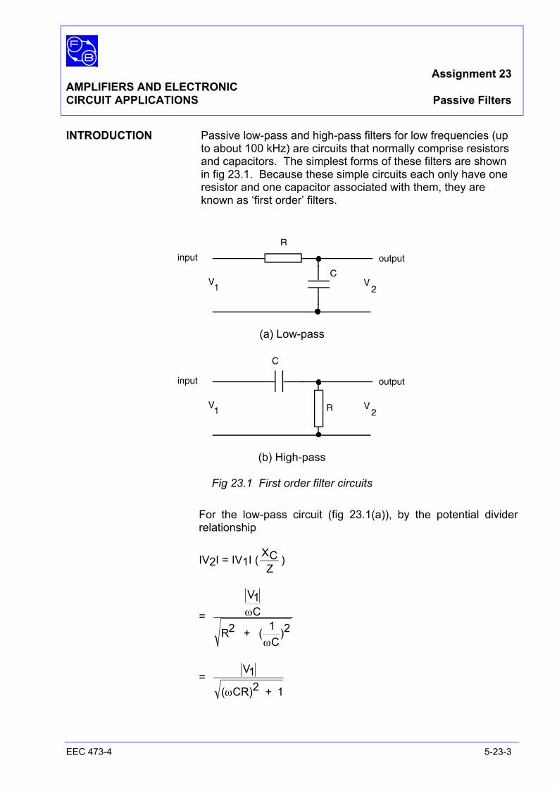
Assignment 23 AMPLIFIERS AND ELECTRONIC CIRCUIT APPLICATIONS Passive Filters
EEC 473-4 5-23-3
INTRODUCTION Passive low-pass and high-pass filters for low frequencies (up to about 100 kHz) are circuits that normally comprise resistors and capacitors. The simplest forms of these filters are shown in fig 23.1. Because these simple circuits each only have one resistor and one capacitor associated with them, they are known as ‘first order’ filters.
(a) Low-pass
(b) High-pass
Fig 23.1 First order filter circuits For the low-pass circuit (fig 23.1(a)), by the potential divider
relationship
IV2I = IV1I ( XCZ
)
= C
R2 + ( 1C
)2
V1ω
ω
= V1
( CR)2 + 1
ω
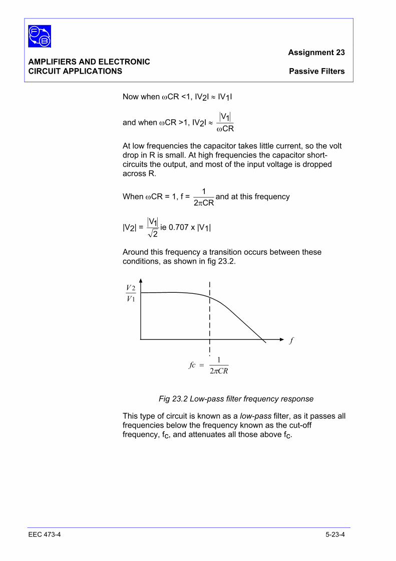
Assignment 23 AMPLIFIERS AND ELECTRONIC CIRCUIT APPLICATIONS Passive Filters
EEC 473-4 5-23-4
Now when ωCR <1, IV2I ≈ IV1I
and when ωCR >1, IV2I ≈ VCR1
ω
At low frequencies the capacitor takes little current, so the volt drop in R is small. At high frequencies the capacitor short-circuits the output, and most of the input voltage is dropped across R.
When ωCR = 1, f = 12 CRπ
and at this frequency
|V2| = V12
ie 0.707 x |V1|
Around this frequency a transition occurs between these conditions, as shown in fig 23.2.
Fig 23.2 Low-pass filter frequency response
This type of circuit is known as a low-pass filter, as it passes all frequencies below the frequency known as the cut-off frequency, fc, and attenuates all those above fc.
CR fc π21
=
1
2
VV
f
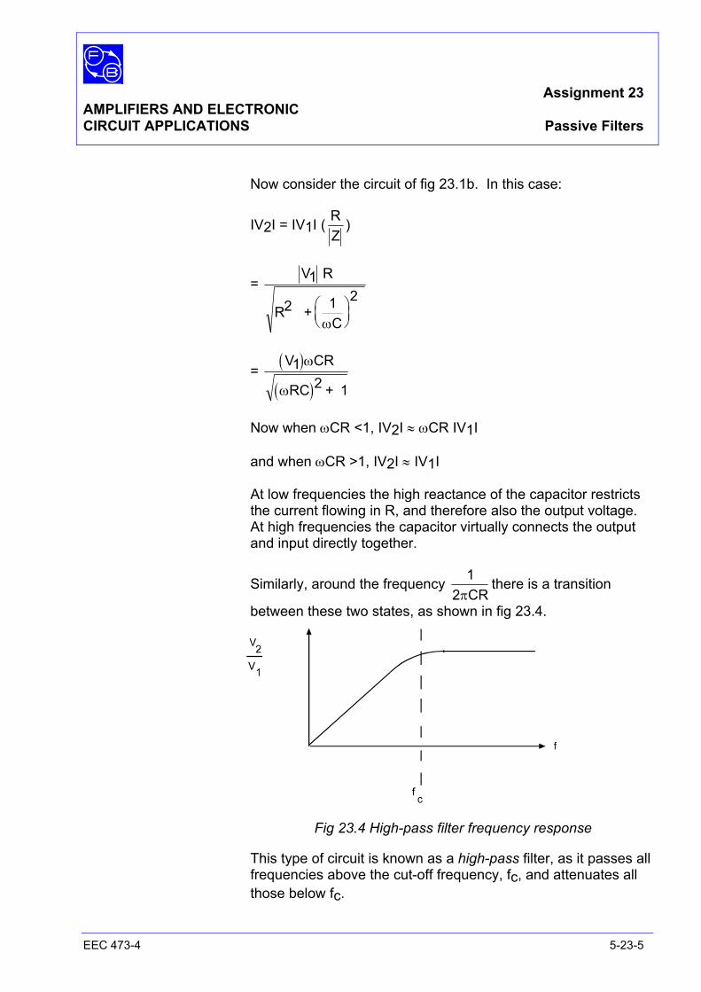
Assignment 23 AMPLIFIERS AND ELECTRONIC CIRCUIT APPLICATIONS Passive Filters
EEC 473-4 5-23-5
Now consider the circuit of fig 23.1b. In this case:
IV2I = IV1I ( RZ
)
= V1 R
R2 + 1C
2
ω
= ( )( )
V1 CR
RC 2 + 1
ω
ω
Now when ωCR <1, IV2I ≈ ωCR IV1I
and when ωCR >1, IV2I ≈ IV1I
At low frequencies the high reactance of the capacitor restricts the current flowing in R, and therefore also the output voltage. At high frequencies the capacitor virtually connects the output and input directly together.
Similarly, around the frequency 12 CRπ
there is a transition
between these two states, as shown in fig 23.4.
Fig 23.4 High-pass filter frequency response
This type of circuit is known as a high-pass filter, as it passes all frequencies above the cut-off frequency, fc, and attenuates all those below fc.
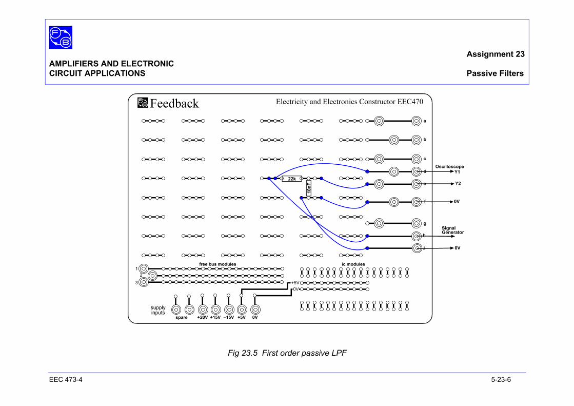
Assignment 23 AMPLIFIERS AND ELECTRONIC CIRCUIT APPLICATIONS Passive Filters
EEC 473-4 5-23-6
Fig 23.5 First order passive LPF
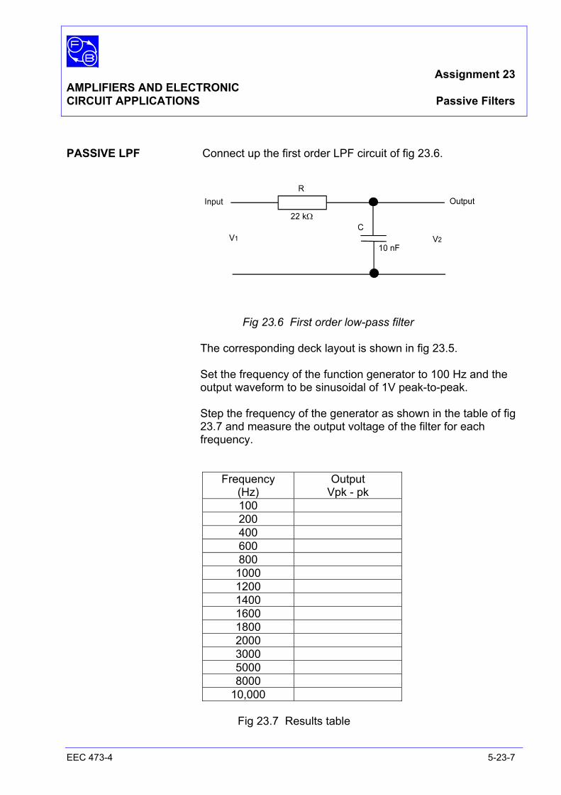
Assignment 23 AMPLIFIERS AND ELECTRONIC CIRCUIT APPLICATIONS Passive Filters
EEC 473-4 5-23-7
PASSIVE LPF Connect up the first order LPF circuit of fig 23.6.
Fig 23.6 First order low-pass filter The corresponding deck layout is shown in fig 23.5. Set the frequency of the function generator to 100 Hz and the
output waveform to be sinusoidal of 1V peak-to-peak. Step the frequency of the generator as shown in the table of fig
23.7 and measure the output voltage of the filter for each frequency.
Frequency (Hz)
Output Vpk - pk
100 200 400 600 800 1000 1200 1400 1600 1800 2000 3000 5000 8000
10,000
Fig 23.7 Results table
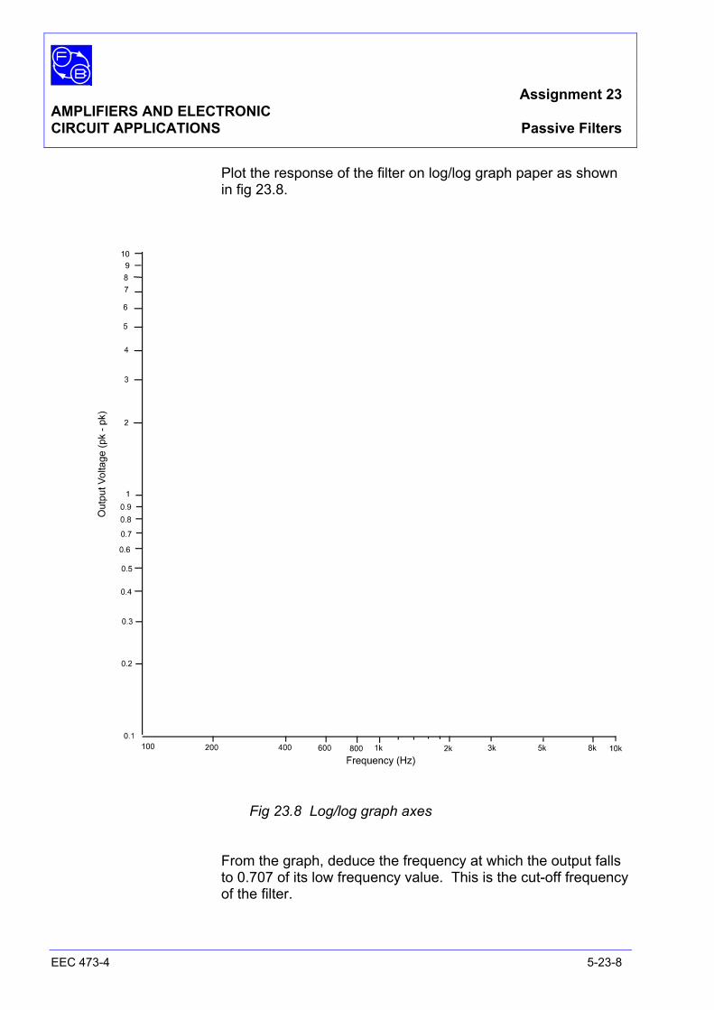
Assignment 23 AMPLIFIERS AND ELECTRONIC CIRCUIT APPLICATIONS Passive Filters
EEC 473-4 5-23-8
Plot the response of the filter on log/log graph paper as shown in fig 23.8.
Fig 23.8 Log/log graph axes
From the graph, deduce the frequency at which the output falls to 0.707 of its low frequency value. This is the cut-off frequency of the filter.

Assignment 23 AMPLIFIERS AND ELECTRONIC CIRCUIT APPLICATIONS Passive Filters
EEC 473-4 5-23-9
Notes
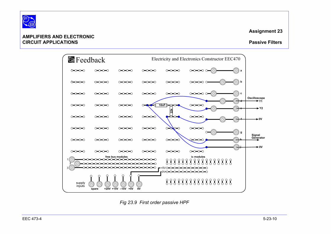
Assignment 23 AMPLIFIERS AND ELECTRONIC CIRCUIT APPLICATIONS Passive Filters
EEC 473-4 5-23-10
Fig 23.9 First order passive HPF
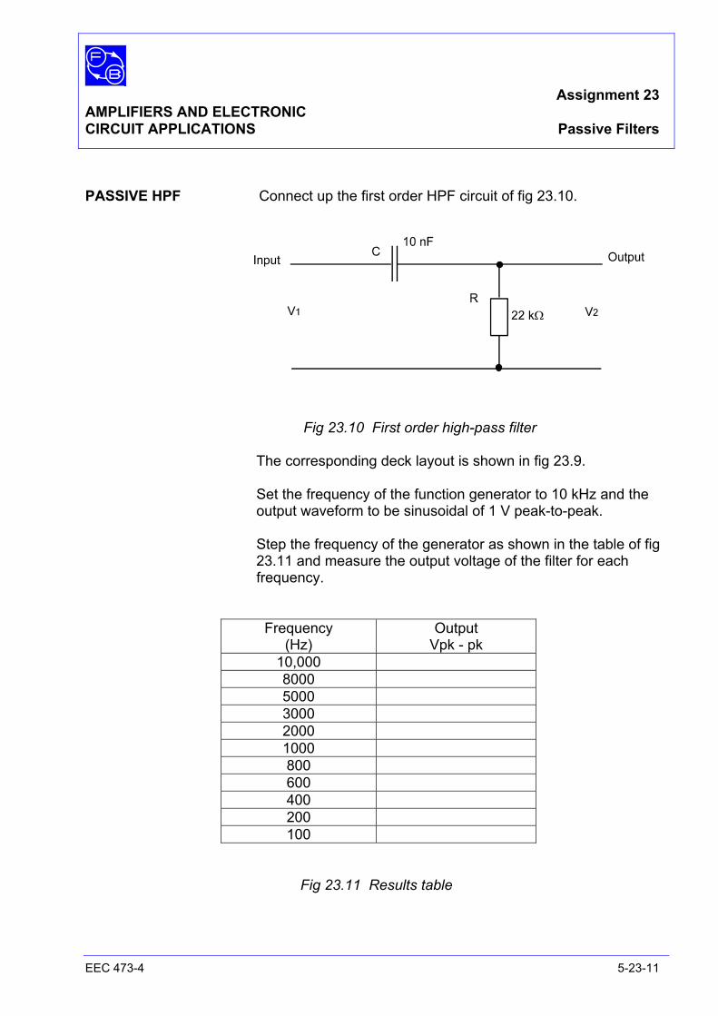
Assignment 23 AMPLIFIERS AND ELECTRONIC CIRCUIT APPLICATIONS Passive Filters
EEC 473-4 5-23-11
PASSIVE HPF Connect up the first order HPF circuit of fig 23.10.
Fig 23.10 First order high-pass filter The corresponding deck layout is shown in fig 23.9. Set the frequency of the function generator to 10 kHz and the
output waveform to be sinusoidal of 1 V peak-to-peak. Step the frequency of the generator as shown in the table of fig
23.11 and measure the output voltage of the filter for each frequency.
Frequency (Hz)
Output Vpk - pk
10,000 8000 5000 3000 2000 1000 800 600 400 200 100
Fig 23.11 Results table
Assignment 23 AMPLIFIERS AND ELECTRONIC CIRCUIT APPLICATIONS Passive Filters
EEC 473-4 5-23-12
Plot the response of the filter on the same sheet of log/log graph paper as shown in fig 23.8 for the LPF.
From the graph, deduce the frequency at which the output falls
to 0.707 of its low frequency value. This is the cut-off frequency of the filter.
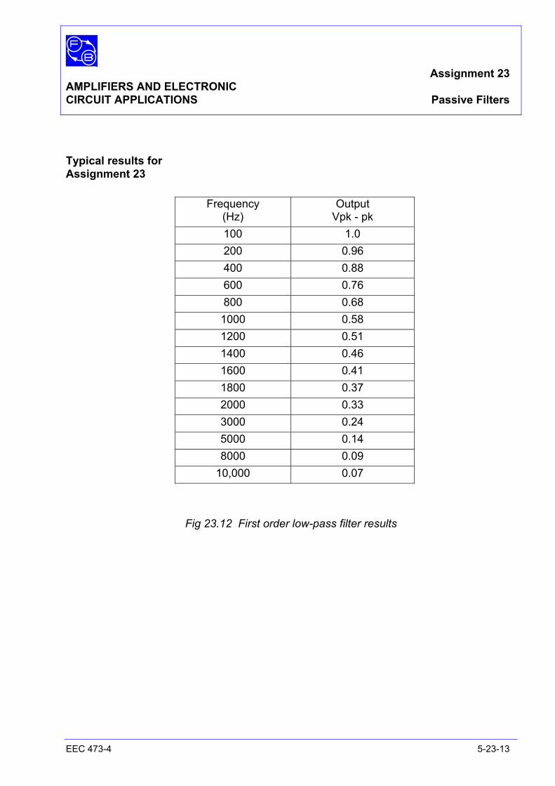
Assignment 23 AMPLIFIERS AND ELECTRONIC CIRCUIT APPLICATIONS Passive Filters
EEC 473-4 5-23-13
Typical results for Assignment 23
Frequency (Hz)
Output Vpk - pk
100 1.0 200 0.96 400 0.88 600 0.76 800 0.68 1000 0.58 1200 0.51 1400 0.46 1600 0.41 1800 0.37 2000 0.33 3000 0.24 5000 0.14 8000 0.09
10,000 0.07
Fig 23.12 First order low-pass filter results
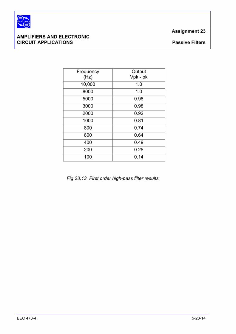
Assignment 23 AMPLIFIERS AND ELECTRONIC CIRCUIT APPLICATIONS Passive Filters
EEC 473-4 5-23-14
Frequency (Hz)
Output Vpk - pk
10,000 1.0 8000 1.0 5000 0.98 3000 0.98 2000 0.92 1000 0.81 800 0.74 600 0.64 400 0.49 200 0.28 100 0.14
Fig 23.13 First order high-pass filter results
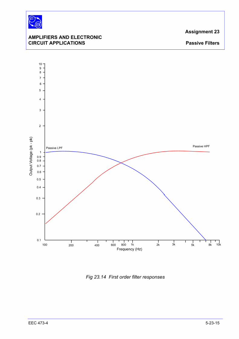
Assignment 23 AMPLIFIERS AND ELECTRONIC CIRCUIT APPLICATIONS Passive Filters
EEC 473-4 5-23-15
Fig 23.14 First order filter responses

Assignment 23 AMPLIFIERS AND ELECTRONIC CIRCUIT APPLICATIONS Passive Filters
EEC 473-4 5-23-16
Notes
Assignment 24 AMPLIFIERS AND ELECTRONIC CIRCUIT APPLICATIONS Active First Order Filters
EEC 473-4 5-24-1
EQUIPMENT REQUIRED Qty Apparatus 1 Electricity & Electronics Constructor
EEC470 1 Circuit Applications Kit EEC473-4
1 Power supply unit ±15 V dc regulated (eg, Feedback Power Supply 92-445 or 92-100 Teknikit Console)
1 Function Generator, Sinusoidal 1 V pk-to-pk, 100 Hz to 10 kHz (eg, Feedback FG601).
1 2–Channel oscilloscope PREREQUISITE ASSIGNMENTS Assignment 23 KNOWLEDGE LEVEL See Prerequisite Assignments.

Assignment 24 AMPLIFIERS AND ELECTRONIC CIRCUIT APPLICATIONS Active First Order Filters
EEC 473-4 5-24-2
Notes
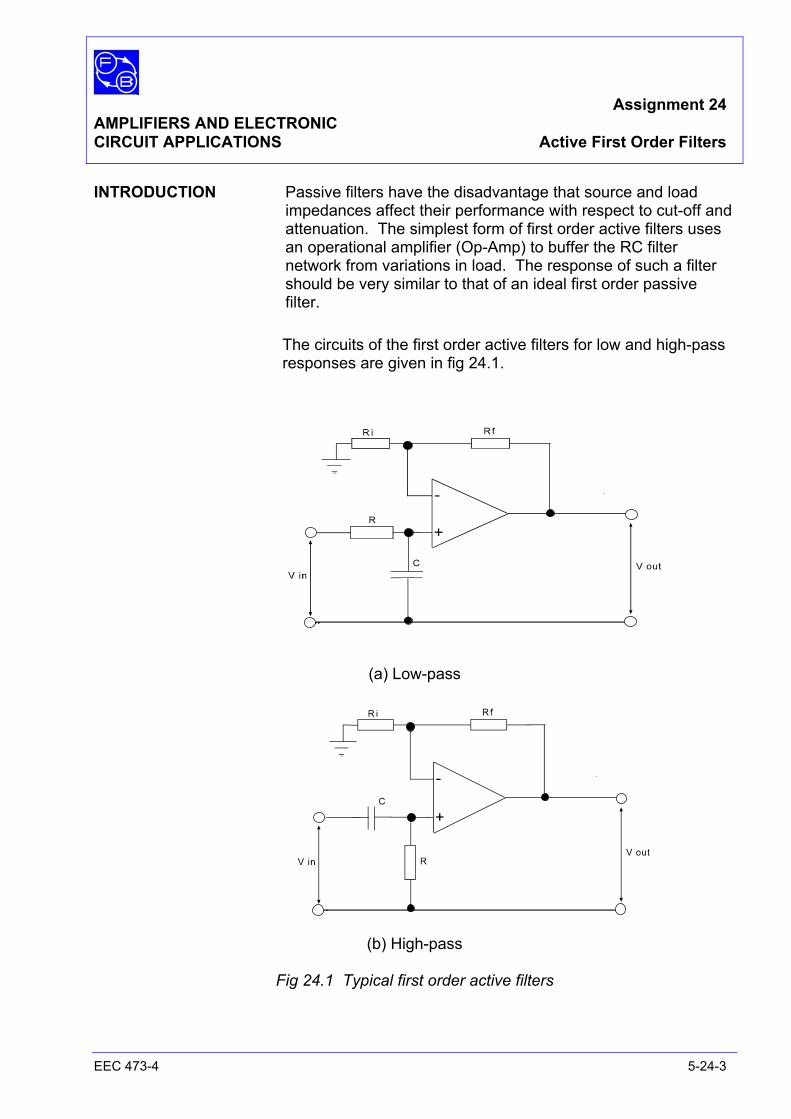
Assignment 24 AMPLIFIERS AND ELECTRONIC CIRCUIT APPLICATIONS Active First Order Filters
EEC 473-4 5-24-3
INTRODUCTION Passive filters have the disadvantage that source and load impedances affect their performance with respect to cut-off and attenuation. The simplest form of first order active filters uses an operational amplifier (Op-Amp) to buffer the RC filter network from variations in load. The response of such a filter should be very similar to that of an ideal first order passive filter.
The circuits of the first order active filters for low and high-pass
responses are given in fig 24.1.
(a) Low-pass
(b) High-pass
Fig 24.1 Typical first order active filters
Assignment 24 AMPLIFIERS AND ELECTRONIC CIRCUIT APPLICATIONS Active First Order Filters
EEC 473-4 5-24-4
You can notice from these circuits that they comprise a passive
first order RC filter followed by an Op-Amp. Note that the Op-Amp circuit is a non-inverting one and that the gain is set by the 15 kΩ (Rf) and 27 kΩ (Ri) resistors. For a non-inverting Op-Amp circuit, the gain is given by:
gain = (1 + Rf/Ri) which for these circuits is: gain = (1 + 15 k/27 k) = 1.56. The theory and mathematics for the filters are the same as
described in Assignment 23, except that the output is amplified 1.56 times by the Op-Amp. The input impedance of the Op-Amp is extremely high and its output impedance very low, so it acts as a very good buffer circuit for the filter.

Assignment 24 AMPLIFIERS AND ELECTRONIC CIRCUIT APPLICATIONS Active First Order Filters
EEC 473-4 5-24-5
Notes
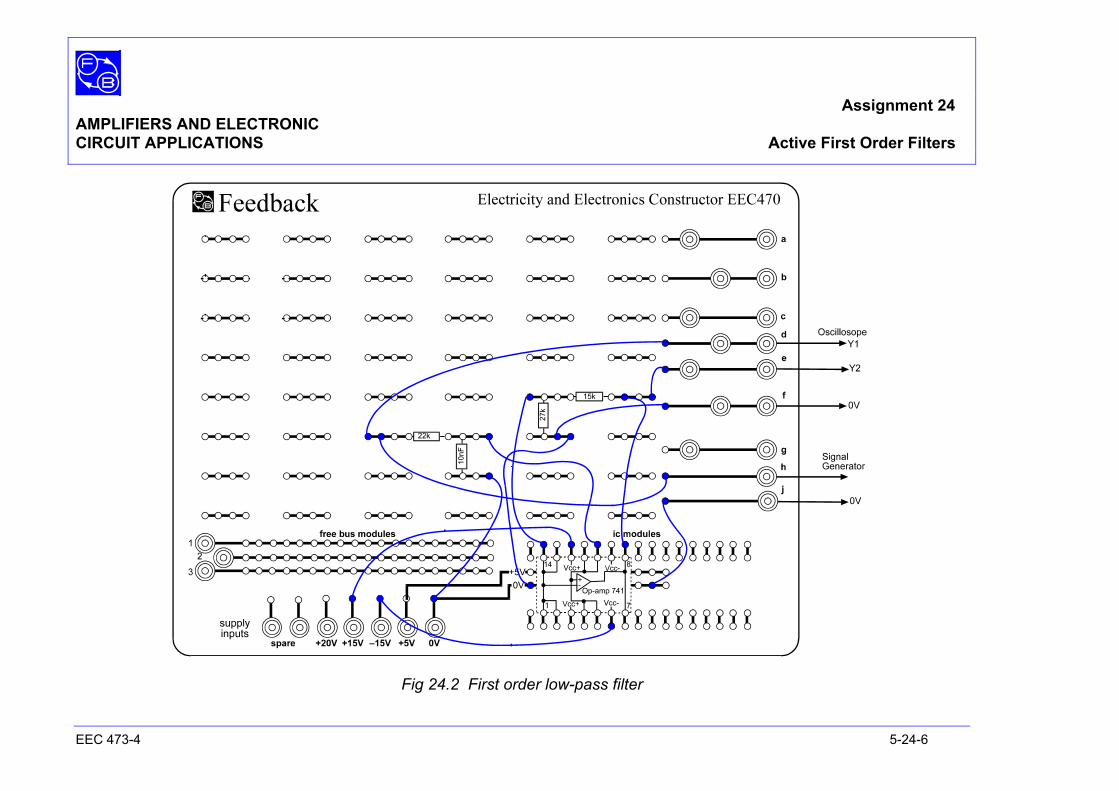
Assignment 24 AMPLIFIERS AND ELECTRONIC CIRCUIT APPLICATIONS Active First Order Filters
EEC 473-4 5-24-6
Fig 24.2 First order low-pass filter
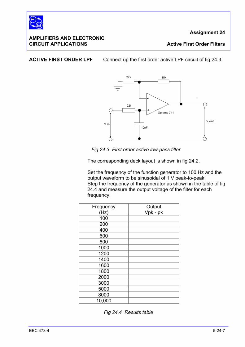
Assignment 24 AMPLIFIERS AND ELECTRONIC CIRCUIT APPLICATIONS Active First Order Filters
EEC 473-4 5-24-7
ACTIVE FIRST ORDER LPF Connect up the first order active LPF circuit of fig 24.3.
Fig 24.3 First order active low-pass filter
The corresponding deck layout is shown in fig 24.2. Set the frequency of the function generator to 100 Hz and the
output waveform to be sinusoidal of 1 V peak-to-peak. Step the frequency of the generator as shown in the table of fig
24.4 and measure the output voltage of the filter for each frequency.
Frequency
(Hz) Output
Vpk - pk 100 200 400 600 800
1000 1200 1400 1600 1800 2000 3000 5000 8000
10,000
Fig 24.4 Results table
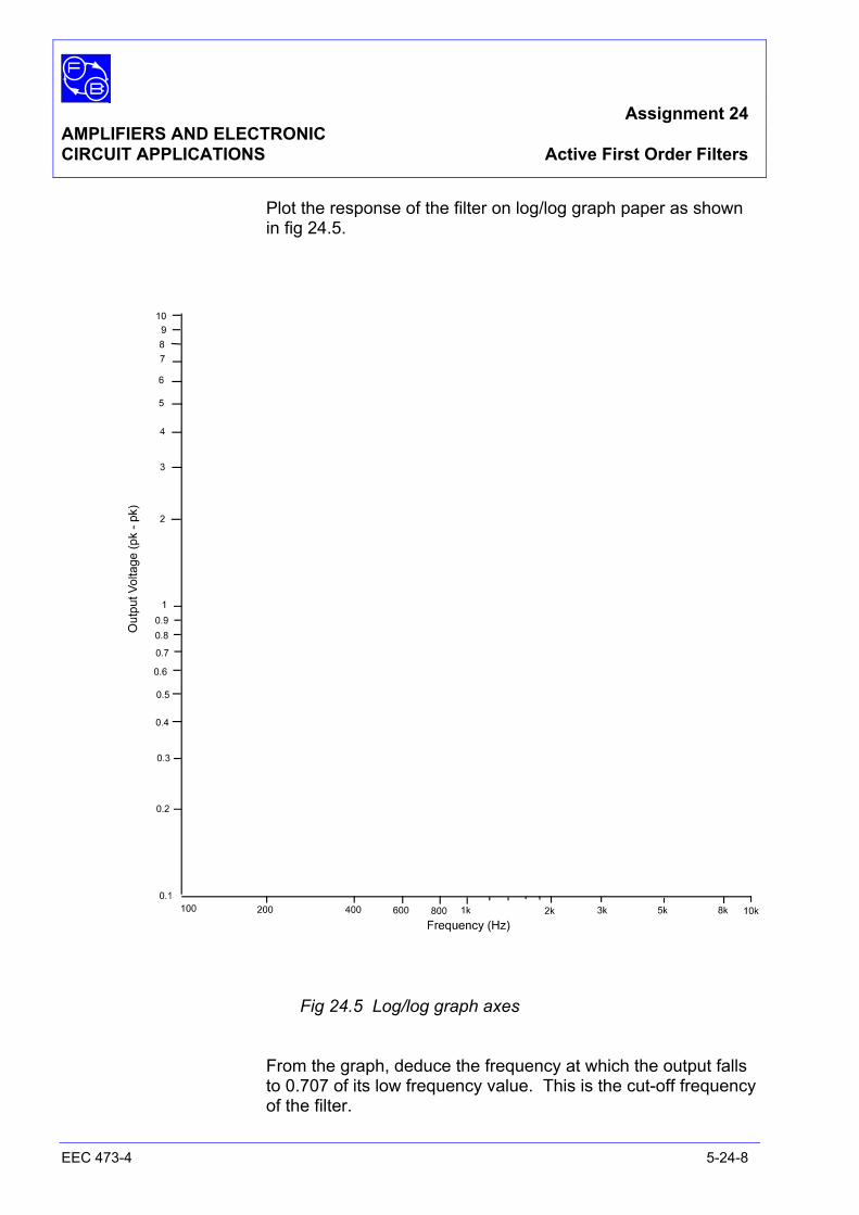
Assignment 24 AMPLIFIERS AND ELECTRONIC CIRCUIT APPLICATIONS Active First Order Filters
EEC 473-4 5-24-8
Plot the response of the filter on log/log graph paper as shown in fig 24.5.
Fig 24.5 Log/log graph axes
From the graph, deduce the frequency at which the output falls to 0.707 of its low frequency value. This is the cut-off frequency of the filter.

Assignment 24 AMPLIFIERS AND ELECTRONIC CIRCUIT APPLICATIONS Active First Order Filters
EEC 473-4 5-24-9
Notes
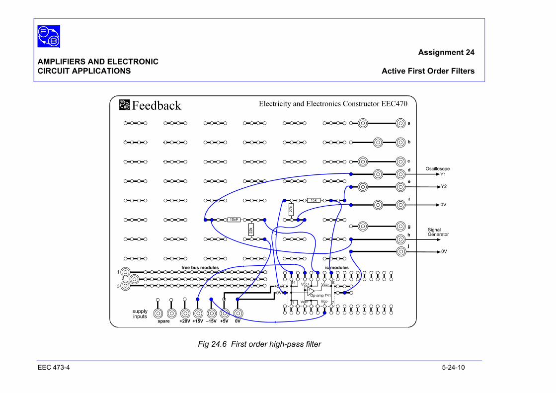
Assignment 24 AMPLIFIERS AND ELECTRONIC CIRCUIT APPLICATIONS Active First Order Filters
EEC 473-4 5-24-10
Fig 24.6 First order high-pass filter
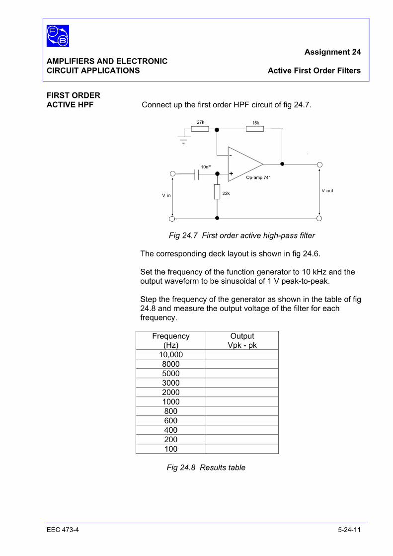
Assignment 24 AMPLIFIERS AND ELECTRONIC CIRCUIT APPLICATIONS Active First Order Filters
EEC 473-4 5-24-11
FIRST ORDER ACTIVE HPF Connect up the first order HPF circuit of fig 24.7.
Fig 24.7 First order active high-pass filter
The corresponding deck layout is shown in fig 24.6. Set the frequency of the function generator to 10 kHz and the
output waveform to be sinusoidal of 1 V peak-to-peak. Step the frequency of the generator as shown in the table of fig
24.8 and measure the output voltage of the filter for each frequency.
Frequency
(Hz) Output
Vpk - pk 10,000 8000 5000 3000 2000 1000 800 600 400 200 100
Fig 24.8 Results table
Assignment 24 AMPLIFIERS AND ELECTRONIC CIRCUIT APPLICATIONS Active First Order Filters
EEC 473-4 5-24-12
Plot the response of the filter on the same sheet of log/log graph paper as shown in fig 24.5 for the LPF.
From the graph, deduce the frequency at which the output falls
to 0.707 of its low frequency value. This is the cut-off frequency of the filter.
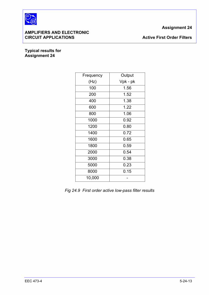
Assignment 24 AMPLIFIERS AND ELECTRONIC CIRCUIT APPLICATIONS Active First Order Filters
EEC 473-4 5-24-13
Typical results for Assignment 24
Frequency (Hz)
Output Vpk - pk
100 1.56 200 1.52 400 1.38 600 1.22 800 1.06 1000 0.92 1200 0.80 1400 0.72 1600 0.65 1800 0.59 2000 0.54 3000 0.38 5000 0.23 8000 0.15
10,000 -
Fig 24.9 First order active low-pass filter results
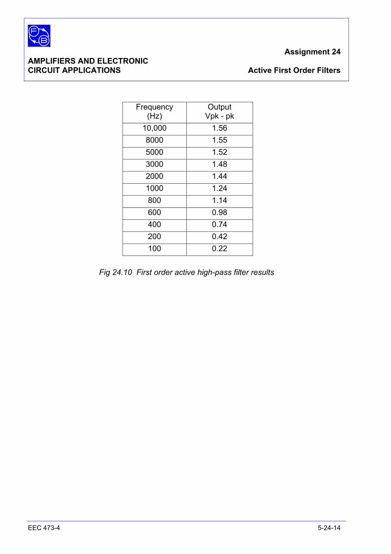
Assignment 24 AMPLIFIERS AND ELECTRONIC CIRCUIT APPLICATIONS Active First Order Filters
EEC 473-4 5-24-14
Frequency
(Hz) Output
Vpk - pk 10,000 1.56 8000 1.55 5000 1.52 3000 1.48 2000 1.44 1000 1.24 800 1.14 600 0.98 400 0.74 200 0.42 100 0.22
Fig 24.10 First order active high-pass filter results
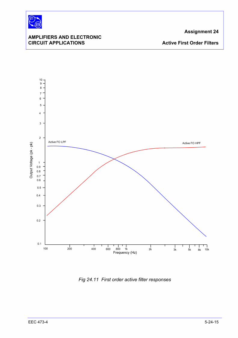
Assignment 24 AMPLIFIERS AND ELECTRONIC CIRCUIT APPLICATIONS Active First Order Filters
EEC 473-4 5-24-15
Fig 24.11 First order active filter responses

Assignment 24 AMPLIFIERS AND ELECTRONIC CIRCUIT APPLICATIONS Active First Order Filters
EEC 473-4 5-24-16
Notes
Assignment 25 AMPLIFIERS AND ELECTRONIC CIRCUIT APPLICATIONS Active Second Order Low- and High-Pass Filters
EEC 473-4 5-25-1
EQUIPMENT REQUIRED Qty Apparatus 1 Electricity & Electronics Constructor
EEC470 1 Circuit Applications Kit EEC473-4
1 Power supply unit ±15 V dc regulated (eg, Feedback Power Supply 92-445 or 92-100 Teknikit Console)
1 Function Generator, Sinusoidal 1 V pk-to-pk, 100 Hz to 10 kHz (eg, Feedback FG601).
1 2–Channel oscilloscope PREREQUISITES Assignment 24 KNOWLEDGE LEVEL See Prerequisite Assignments.
Assignment 25 AMPLIFIERS AND ELECTRONIC CIRCUIT APPLICATIONS Active Second Order Low- and High-Pass Filters
EEC 473-4 5-25-2
Notes
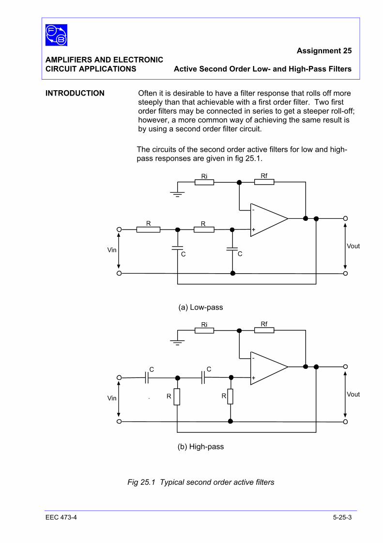
Assignment 25 AMPLIFIERS AND ELECTRONIC CIRCUIT APPLICATIONS Active Second Order Low- and High-Pass Filters
EEC 473-4 5-25-3
INTRODUCTION Often it is desirable to have a filter response that rolls off more steeply than that achievable with a first order filter. Two first order filters may be connected in series to get a steeper roll-off; however, a more common way of achieving the same result is by using a second order filter circuit.
The circuits of the second order active filters for low and high-
pass responses are given in fig 25.1.
(a) Low-pass
(b) High-pass
Fig 25.1 Typical second order active filters
Assignment 25 AMPLIFIERS AND ELECTRONIC CIRCUIT APPLICATIONS Active Second Order Low- and High-Pass Filters
EEC 473-4 5-25-4
Notice that these second order circuits comprise two passive
first order RC networks with feedback from the Op-Amp. This type of circuit is known as a ‘Sallen-Key’ filter, named after its originators. As in Assignment 24, the Op-Amp circuit is a non-inverting one and the gain is set by the 15 kΩ (Rf) and 27 kΩ (Ri) resistors. The gain is given by:
gain = (1 + Rf/Ri) which for these circuits is (1 + 15 kΩ/27 kΩ) = 1.56. Because the two RC filter sections are effectively in series the
roll-of of the filter will be at twice the rate of a first-order circuit. For equal values of R and C in the two sections of the filter, the
cut-off frequency for such a circuit is given by 1/2πRC As well as providing gain and feedback, the input impedance of
the Op-Amp is extremely high and its output impedance very low, so it acts as a very good buffer circuit for the filter.

Assignment 25 AMPLIFIERS AND ELECTRONIC CIRCUIT APPLICATIONS Active Second Order Low- and High-Pass Filters
EEC 473-4 5-25-5
Notes
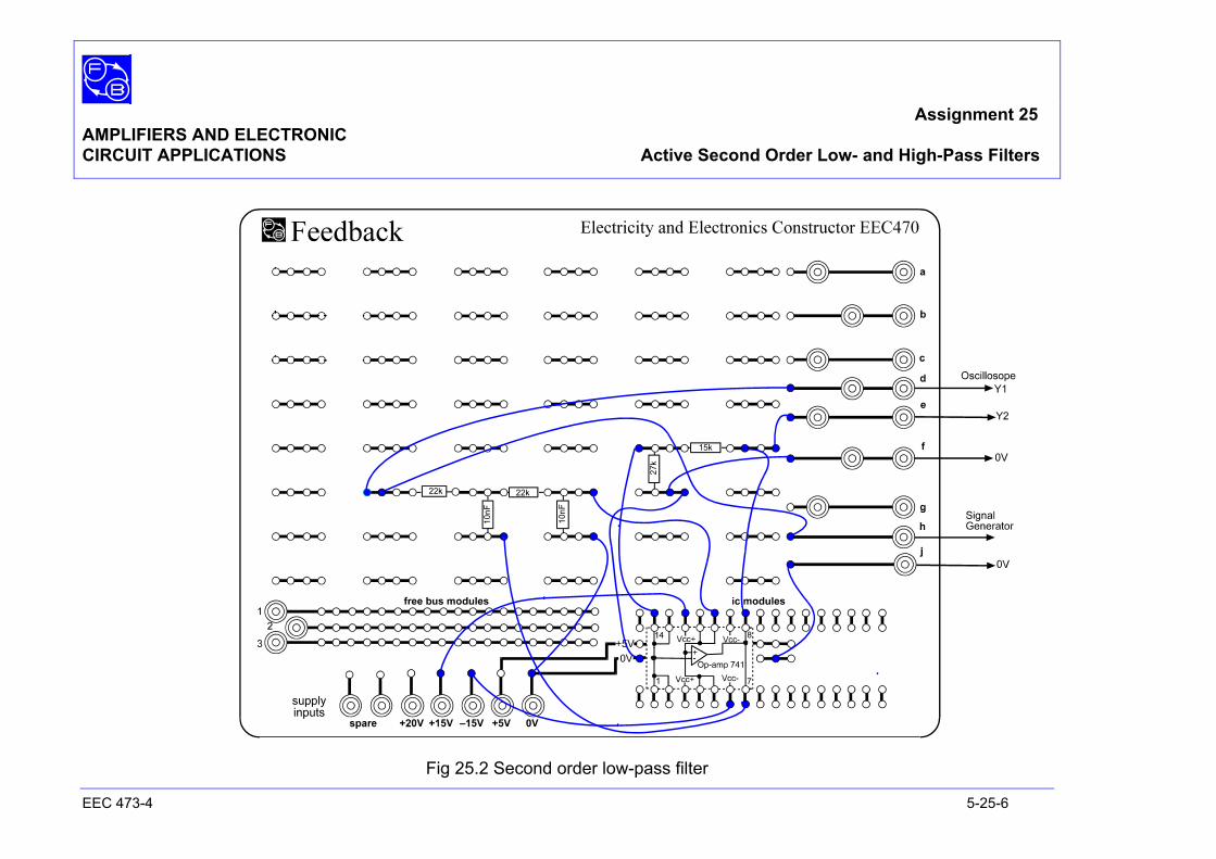
Assignment 25 AMPLIFIERS AND ELECTRONIC CIRCUIT APPLICATIONS Active Second Order Low- and High-Pass Filters
EEC 473-4 5-25-6
Fig 25.2 Second order low-pass filter
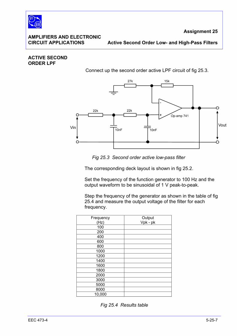
Assignment 25 AMPLIFIERS AND ELECTRONIC CIRCUIT APPLICATIONS Active Second Order Low- and High-Pass Filters
EEC 473-4 5-25-7
ACTIVE SECOND ORDER LPF Connect up the second order active LPF circuit of fig 25.3.
Fig 25.3 Second order active low-pass filter
The corresponding deck layout is shown in fig 25.2. Set the frequency of the function generator to 100 Hz and the
output waveform to be sinusoidal of 1 V peak-to-peak. Step the frequency of the generator as shown in the table of fig
25.4 and measure the output voltage of the filter for each frequency.
Frequency
(Hz) Output
Vpk - pk 100 200 400 600 800
1000 1200 1400 1600 1800 2000 3000 5000 8000
10,000
Fig 25.4 Results table
Assignment 25 AMPLIFIERS AND ELECTRONIC CIRCUIT APPLICATIONS Active Second Order Low- and High-Pass Filters
EEC 473-4 5-25-8
Plot the response of the filter on log/log graph paper as shown in fig 25.5.
Fig 25.5 Log/log graph axes
From the graph, deduce the frequency at which the output falls to 0.707 of its low frequency value. This is the cut-off frequency of the filter.

Assignment 25 AMPLIFIERS AND ELECTRONIC CIRCUIT APPLICATIONS Active Second Order Low- and High-Pass Filters
EEC 473-4 5-25-9
Notes
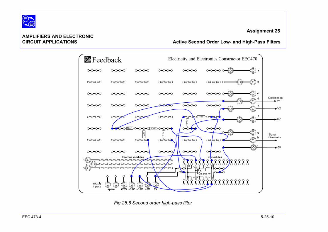
Assignment 25 AMPLIFIERS AND ELECTRONIC CIRCUIT APPLICATIONS Active Second Order Low- and High-Pass Filters
EEC 473-4 5-25-10
Fig 25.6 Second order high-pass filter
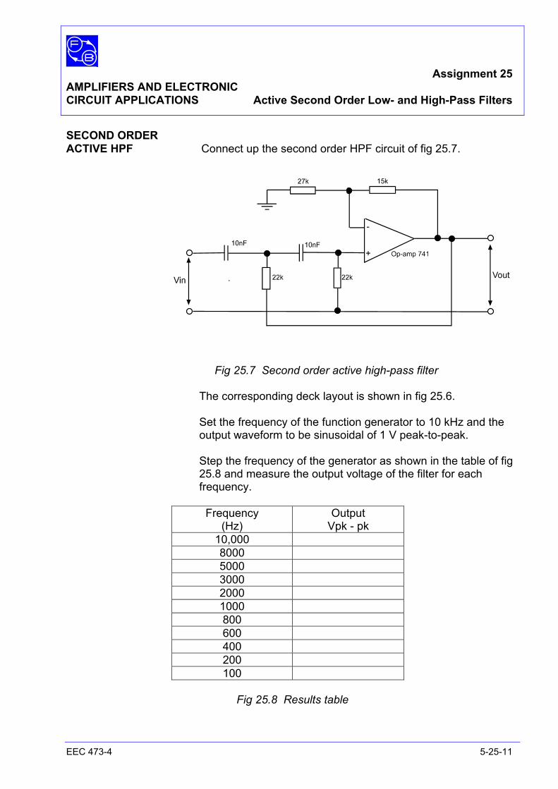
Assignment 25 AMPLIFIERS AND ELECTRONIC CIRCUIT APPLICATIONS Active Second Order Low- and High-Pass Filters
EEC 473-4 5-25-11
SECOND ORDER ACTIVE HPF Connect up the second order HPF circuit of fig 25.7.
Fig 25.7 Second order active high-pass filter The corresponding deck layout is shown in fig 25.6. Set the frequency of the function generator to 10 kHz and the
output waveform to be sinusoidal of 1 V peak-to-peak. Step the frequency of the generator as shown in the table of fig
25.8 and measure the output voltage of the filter for each frequency.
Frequency
(Hz) Output
Vpk - pk 10,000 8000 5000 3000 2000 1000 800 600 400 200 100
Fig 25.8 Results table
Assignment 25 AMPLIFIERS AND ELECTRONIC CIRCUIT APPLICATIONS Active Second Order Low- and High-Pass Filters
EEC 473-4 5-25-12
Plot the response of the filter on the same sheet of log/log graph paper as shown in fig 25.5 for the LPF.
From the graph, deduce the frequency at which the output falls
to 0.707 of its low frequency value. This is the cut-off frequency of the filter.
Assignment 25 AMPLIFIERS AND ELECTRONIC CIRCUIT APPLICATIONS Active Second Order Low- and High-Pass Filters
EEC 473-4 5-25-13
Typical results for Assignment 25
Frequency (Hz)
Output Vpk - pk
100 1.56 200 1.56 400 1.52 600 1.32 800 1.0 1000 0.74 1200 0.54 1400 0.41 1600 0.32 1800 0.25 2000 0.21 3000 0.09 5000 0.07 8000 0.03
10,000 -
Fig 25.9 Second order active low-pass filter results Frequency
(Hz) Output
Vpk - pk 10,000 1.56 8000 1.56 5000 1.54 3000 1.54 2000 1.50 1000 1.30 800 1.12 600 0.82 400 0.43 200 0.12 100 0.06
Fig 25.10 Second order active high-pass filter results
Assignment 25 AMPLIFIERS AND ELECTRONIC CIRCUIT APPLICATIONS Active Second Order Low- and High-Pass Filters
EEC 473-4 5-25-14
Fig 25.11 Second order active filter responses
Assignment 26 AMPLIFIERS AND ELECTRONIC CIRCUIT APPLICATIONS Active Second Order Bandpass Filters
EEC 473-4 5-26-1
INTRODUCTION A common requirement is for a filter to pass a frequency, or a band of frequencies, and reject all others. This requires a bandpass response.
A bandpass response can be achieved by cascading low-pass
and high-pass filter sections. An active circuit that effectively achieves this is shown in fig 26.1. Because there are two RC networks associated with the circuit, it is a second order circuit.
Fig 26.1 A typical second order active bandpass filter In fig 26.1, the Op-Amp circuit is an inverting one and the
bandpass gain is set by the resistor values. They also determine the bandwidth of the circuit.
Note:
The values of the components in fig 26.1 are what is known as ‘normalised values’, Practical values are calculated by multiplying, or dividing, these normalised values by certain factors.
The relationship between the bandwidth (BW) and the
frequency of the peak of the response (f0) is given by the factor ‘Q’, where
Q = f0 / BW
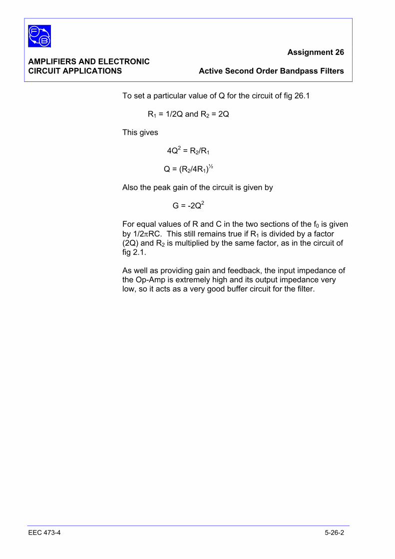
Assignment 26 AMPLIFIERS AND ELECTRONIC CIRCUIT APPLICATIONS Active Second Order Bandpass Filters
EEC 473-4 5-26-2
To set a particular value of Q for the circuit of fig 26.1
R1 = 1/2Q and R2 = 2Q
This gives
4Q2 = R2/R1
Q = (R2/4R1)½ Also the peak gain of the circuit is given by
G = -2Q2
For equal values of R and C in the two sections of the f0 is given by 1/2πRC. This still remains true if R1 is divided by a factor (2Q) and R2 is multiplied by the same factor, as in the circuit of fig 2.1.
As well as providing gain and feedback, the input impedance of
the Op-Amp is extremely high and its output impedance very low, so it acts as a very good buffer circuit for the filter.

Assignment 26 AMPLIFIERS AND ELECTRONIC CIRCUIT APPLICATIONS Active Second Order Bandpass Filters
EEC 473-4 5-26-3
Notes
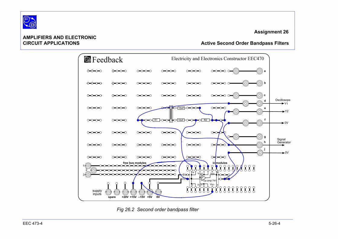
Assignment 26 AMPLIFIERS AND ELECTRONIC CIRCUIT APPLICATIONS Active Second Order Bandpass Filters
EEC 473-4 5-26-4
Fig 26.2 Second order bandpass filter
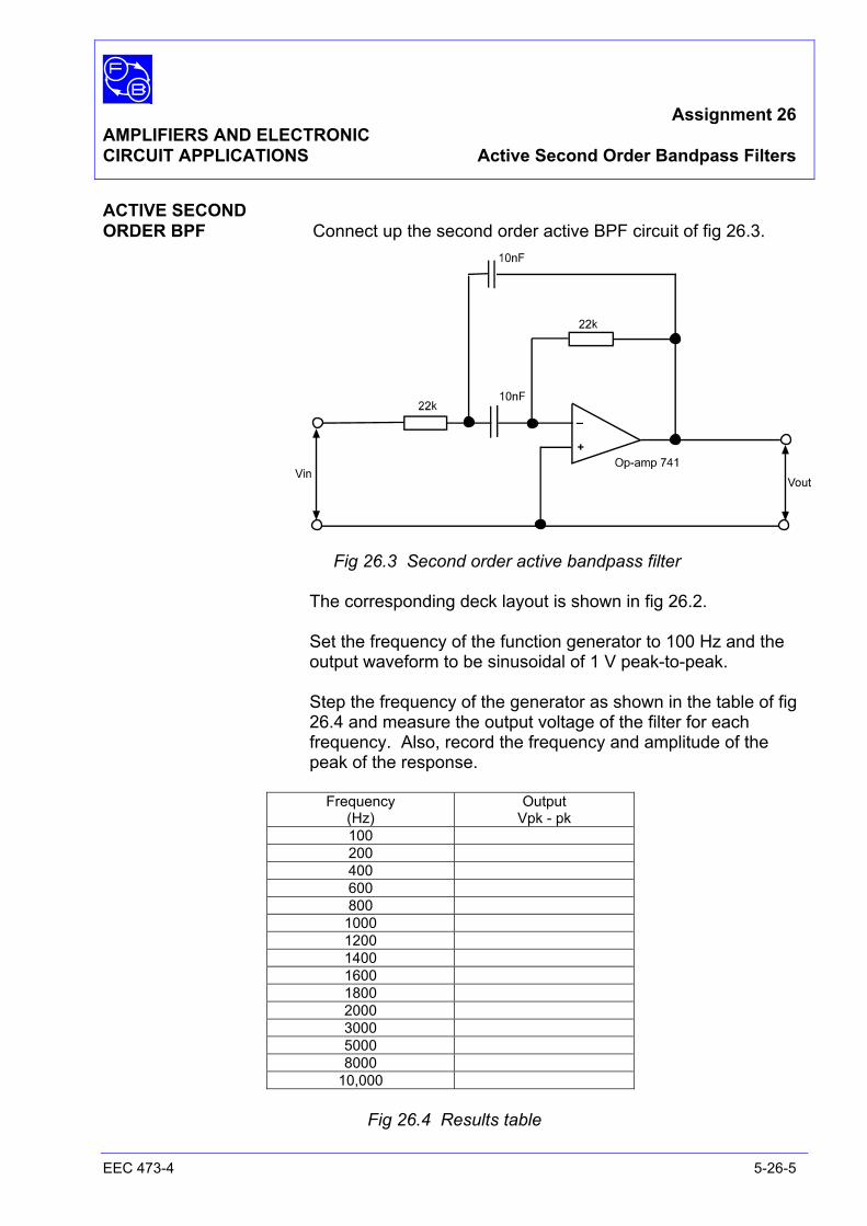
Assignment 26 AMPLIFIERS AND ELECTRONIC CIRCUIT APPLICATIONS Active Second Order Bandpass Filters
EEC 473-4 5-26-5
ACTIVE SECOND ORDER BPF Connect up the second order active BPF circuit of fig 26.3.
Fig 26.3 Second order active bandpass filter
The corresponding deck layout is shown in fig 26.2. Set the frequency of the function generator to 100 Hz and the
output waveform to be sinusoidal of 1 V peak-to-peak. Step the frequency of the generator as shown in the table of fig
26.4 and measure the output voltage of the filter for each frequency. Also, record the frequency and amplitude of the peak of the response.
Frequency
(Hz) Output
Vpk - pk 100 200 400 600 800
1000 1200 1400 1600 1800 2000 3000 5000 8000
10,000
Fig 26.4 Results table
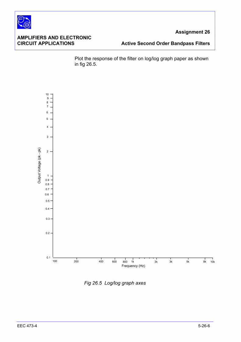
Assignment 26 AMPLIFIERS AND ELECTRONIC CIRCUIT APPLICATIONS Active Second Order Bandpass Filters
EEC 473-4 5-26-6
Plot the response of the filter on log/log graph paper as shown in fig 26.5.
Fig 26.5 Log/log graph axes
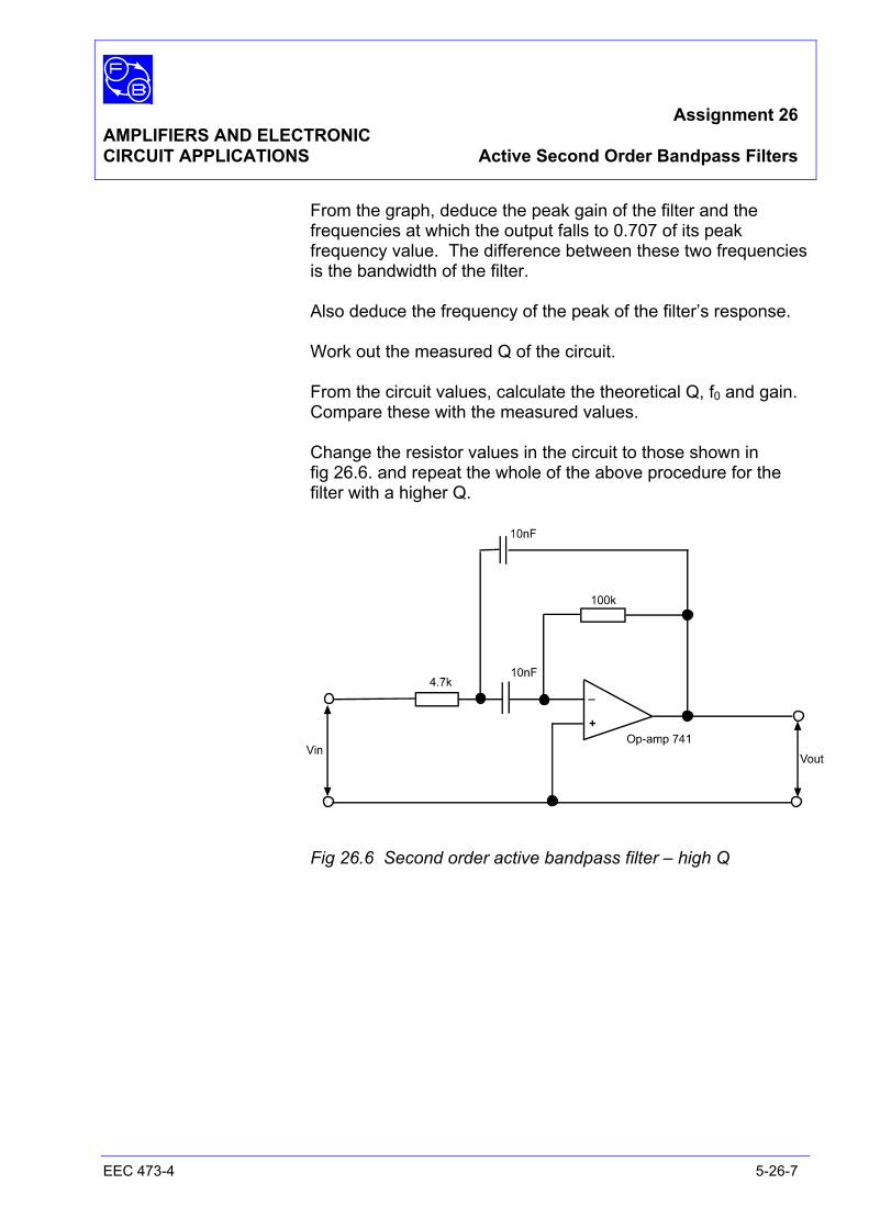
Assignment 26 AMPLIFIERS AND ELECTRONIC CIRCUIT APPLICATIONS Active Second Order Bandpass Filters
EEC 473-4 5-26-7
From the graph, deduce the peak gain of the filter and the frequencies at which the output falls to 0.707 of its peak frequency value. The difference between these two frequencies is the bandwidth of the filter.
Also deduce the frequency of the peak of the filter’s response. Work out the measured Q of the circuit. From the circuit values, calculate the theoretical Q, f0 and gain.
Compare these with the measured values. Change the resistor values in the circuit to those shown in
fig 26.6. and repeat the whole of the above procedure for the filter with a higher Q.
Fig 26.6 Second order active bandpass filter – high Q
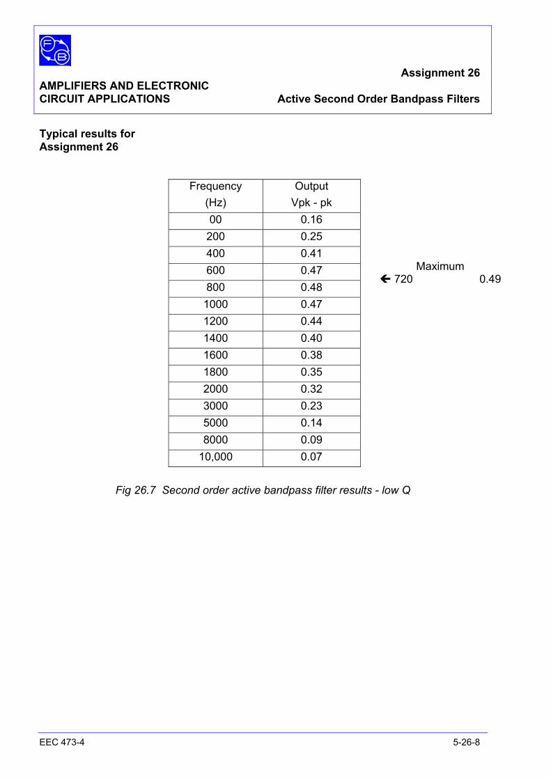
Assignment 26 AMPLIFIERS AND ELECTRONIC CIRCUIT APPLICATIONS Active Second Order Bandpass Filters
EEC 473-4 5-26-8
Typical results for Assignment 26
Frequency (Hz)
Output Vpk - pk
00 0.16 200 0.25 400 0.41 600 0.47 800 0.48
1000 0.47 1200 0.44 1400 0.40 1600 0.38 1800 0.35 2000 0.32 3000 0.23 5000 0.14 8000 0.09
10,000 0.07
Fig 26.7 Second order active bandpass filter results - low Q
Maximum 720 0.49
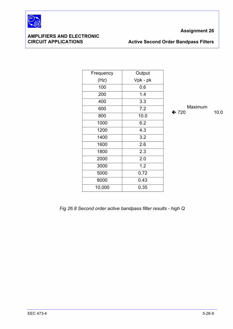
Assignment 26 AMPLIFIERS AND ELECTRONIC CIRCUIT APPLICATIONS Active Second Order Bandpass Filters
EEC 473-4 5-26-9
Frequency (Hz)
Output Vpk - pk
100 0.6 200 1.4 400 3.3 600 7.2 800 10.0
1000 6.2 1200 4.3 1400 3.2 1600 2.6 1800 2.3 2000 2.0 3000 1.2 5000 0.72 8000 0.43
10,000 0.35
Fig 26.8 Second order active bandpass filter results - high Q
Maximum 720 10.0
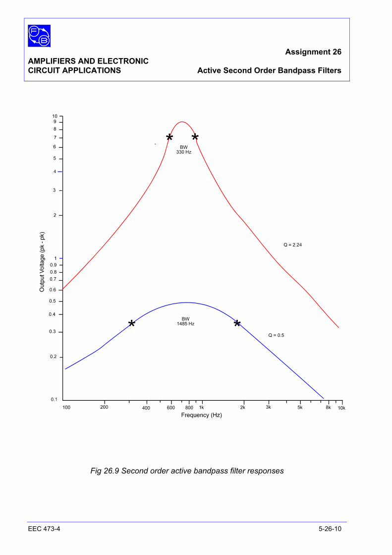
Assignment 26 AMPLIFIERS AND ELECTRONIC CIRCUIT APPLICATIONS Active Second Order Bandpass Filters
EEC 473-4 5-26-10
Fig 26.9 Second order active bandpass filter responses
Section 6 AMPLIFIERS AND ELECTRONIC CIRCUIT APPLICATIONS Further Assignments
EEC 473-4 6-1
Further Assignments The following Assignments can be regarded as optional to
extend understanding of the subject matter presented in the preceding sections

Section 6 AMPLIFIERS AND ELECTRONIC CIRCUIT APPLICATIONS Further Assignments
EEC 473-4 6-2
Notes
Assignment 27 AMPLIFIERS AND ELECTRONIC CIRCUIT APPLICATIONS The Emitter Follower
EEC 473-4 6-27-1
OBJECTIVES 1 To familiarise the student with the Common Collector (Emitter Follower) connection of a transistor.
2 To familiarise the student with the techniques for measuring input and output impedances for a transistor stage.
EQUIPMENT REQUIRED Qty Apparatus
1 Electricity & Electronics Constructor EEC470
1 Amplifiers and Circuit Applications Kit EEC473-4
1 Power supply unit 0 to 20 V variable dc regulated. (eg, Feedback Power Supply 92-445or Teknikit Console 92-100)
1 Oscilloscope, general purpose 20 MHz
1 Sinewave generator, 1 kHz
PREREQUISITE ASSIGNMENTS Basic Electricity and Electronics EEC471-2,
Assignment 34
KNOWLEDGE LEVEL Before working this assignment you should:
Understand the meaning of the terms Gain, Impedance and Phase Shift as applied to an amplifier circuit.

Assignment 27 AMPLIFIERS AND ELECTRONIC CIRCUIT APPLICATIONS The Emitter Follower
EEC 473-4 6-27-2
Notes
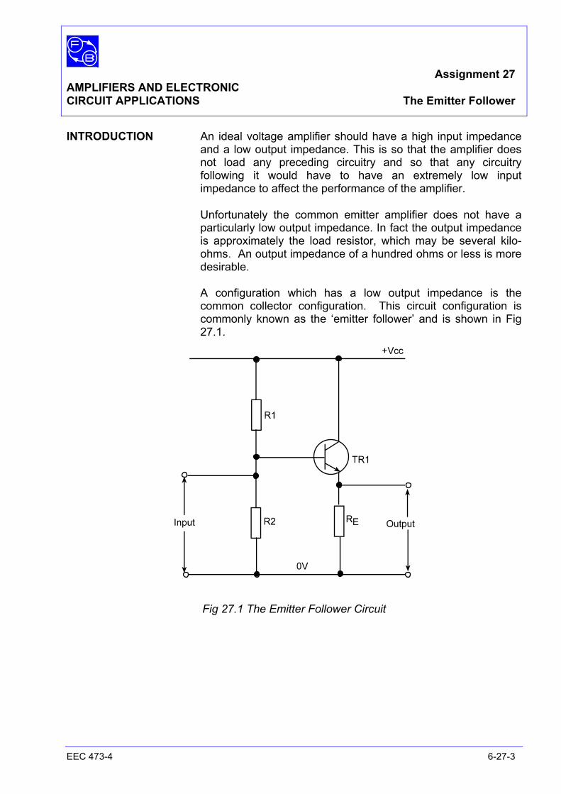
Assignment 27 AMPLIFIERS AND ELECTRONIC CIRCUIT APPLICATIONS The Emitter Follower
EEC 473-4 6-27-3
INTRODUCTION An ideal voltage amplifier should have a high input impedance and a low output impedance. This is so that the amplifier does not load any preceding circuitry and so that any circuitry following it would have to have an extremely low input impedance to affect the performance of the amplifier.
Unfortunately the common emitter amplifier does not have a particularly low output impedance. In fact the output impedance is approximately the load resistor, which may be several kilo-ohms. An output impedance of a hundred ohms or less is more desirable. A configuration which has a low output impedance is the common collector configuration. This circuit configuration is commonly known as the ‘emitter follower’ and is shown in Fig 27.1.
Fig 27.1 The Emitter Follower Circuit
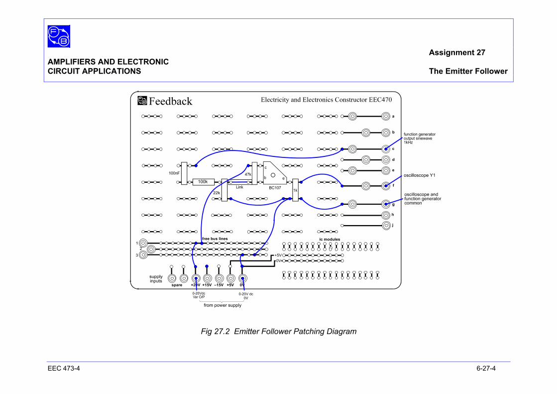
Assignment 27 AMPLIFIERS AND ELECTRONIC CIRCUIT APPLICATIONS The Emitter Follower
EEC 473-4 6-27-4
Fig 27.2 Emitter Follower Patching Diagram
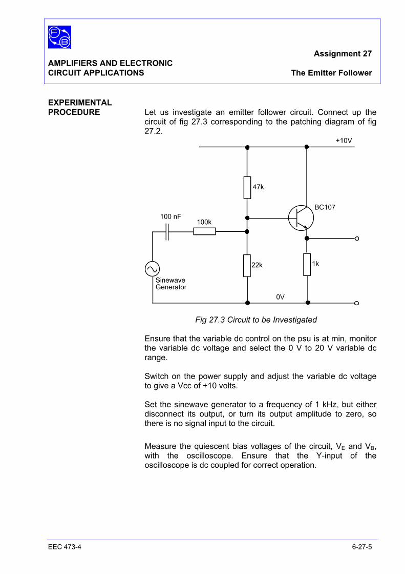
Assignment 27 AMPLIFIERS AND ELECTRONIC CIRCUIT APPLICATIONS The Emitter Follower
EEC 473-4 6-27-5
EXPERIMENTAL PROCEDURE Let us investigate an emitter follower circuit. Connect up the
circuit of fig 27.3 corresponding to the patching diagram of fig 27.2.
Fig 27.3 Circuit to be Investigated Ensure that the variable dc control on the psu is at min, monitor the variable dc voltage and select the 0 V to 20 V variable dc range. Switch on the power supply and adjust the variable dc voltage to give a Vcc of +10 volts. Set the sinewave generator to a frequency of 1 kHz, but either disconnect its output, or turn its output amplitude to zero, so there is no signal input to the circuit.
Measure the quiescent bias voltages of the circuit, VE and VB, with the oscilloscope. Ensure that the Y-input of the oscilloscope is dc coupled for correct operation.
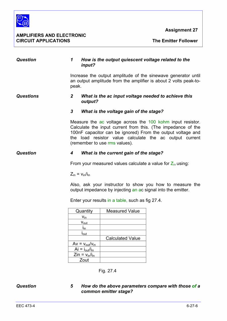
Assignment 27 AMPLIFIERS AND ELECTRONIC CIRCUIT APPLICATIONS The Emitter Follower
EEC 473-4 6-27-6
Question 1 How is the output quiescent voltage related to the input?
Increase the output amplitude of the sinewave generator until an output amplitude from the amplifier is about 2 volts peak-to-peak.
Questions 2 What is the ac input voltage needed to achieve this output?
3 What is the voltage gain of the stage? Measure the ac voltage across the 100 kohm input resistor. Calculate the input current from this. (The impedance of the 100nF capacitor can be ignored) From the output voltage and the load resistor value calculate the ac output current (remember to use rms values).
Question 4 What is the current gain of the stage? From your measured values calculate a value for Zin using: Zin = vin/iin Also, ask your instructor to show you how to measure the output impedance by injecting an ac signal into the emitter. Enter your results in a table, such as fig 27.4.
Quantity Measured Value vin vout iin iout
Calculated Value Av = vout/vin Ai = iout/iin Zin = vin/iin
Zout
Fig. 27.4
Question 5 How do the above parameters compare with those of a common emitter stage?
Assignment 27 AMPLIFIERS AND ELECTRONIC CIRCUIT APPLICATIONS The Emitter Follower
EEC 473-4 6-27-7
From these expressions it can be seen that current gain for the emitter follower is high, and is approximately the same in magnitude as for the C.E stage, but there is no phase reversal (Ai is positive) for the emitter follower. Also the input resistance is very similar to that for the C.E stage. The voltage gain, however, is very nearly unity as hie/zin is very small. And the output resistance is very low, being approximately (Rs + hie) divided by hfe.
PRACTICAL CONSIDERATIONS AND APPLICATIONS The common collector, or emitter follower connected transistor
is the second most used connection.
The common collector connection gives the highest input resistance of the three connections, and also gives the lowest output resistance of the three connections. These are exactly what are needed in a voltage amplifier, but unfortunately the emitter follower has a voltage gain of less than unity. This of course makes it unsuitable for use as a voltage amplifier on its own. The emitter follower connected stage is thus normally used in conjunction with voltage amplifying stages (which are often common emitter connected), usually as the output stage to provide the low resistance output needed. It is also often used as a 'buffer' stage between a high impedance source and a low impedance load; and because of its high current gain it finds application in output stages of audio amplifiers driving low impedance loudspeakers, and in such circuits as relay and motor drivers which rely on current drive. The emitter follower does not give a phase reversal from input to output.
Assignment 27 AMPLIFIERS AND ELECTRONIC CIRCUIT APPLICATIONS The Emitter Follower
EEC 473-4 6-27-8
Notes
Assignment 28 AMPLIFIERS AND ELECTRONIC CIRCUIT APPLICATIONS The Common Base Connection
EEC 473-4 6-28-1
OBJECTIVES 1 To familiarise the student with the Common Base connection of a transistor.
2 To familiarise the student with the techniques for measuring input and output impedances for a transistor stage.
EQUIPMENT REQUIRED Qty Apparatus
1 Electricity & Electronics Constructor EEC470
1 Amplifiers and Circuit Applications Kit EEC473-4
1 Power supply unit 0 to 20 V variable dc regulated. (eg, Feedback Power Supply 92-445 or Teknikit Console 92-100)
1 Oscilloscope, general purpose 20 MHz
1 Sinewave generator, 1 kHz
PREREQUISITE ASSIGNMENTS Basic Electricity and Electronics EEC471-2,
Assignment 34
KNOWLEDGE LEVEL Before working this assignment you should:
Understand the meaning of the terms Gain, Impedance and Phase Shift as applied to an amplifier circuit.

Assignment 28 AMPLIFIERS AND ELECTRONIC CIRCUIT APPLICATIONS The Common Base Connection
EEC 473-4 6-28-2
Notes
Assignment 28 AMPLIFIERS AND ELECTRONIC CIRCUIT APPLICATIONS The Common Base Connection
EEC 473-4 6-28-3
INTRODUCTION The common base connection is not a particularly commonly used connection for a transistor. However, there are applications where it is useful. The input to a common base stage is between emitter and base and is low impedance. The output is taken from the collector and has a medium to high impedance. This means that such a stage cannot be driven from a source that has high impedance without significantly loading it. The common base connection is only of use in circuits where the source impedance is low.
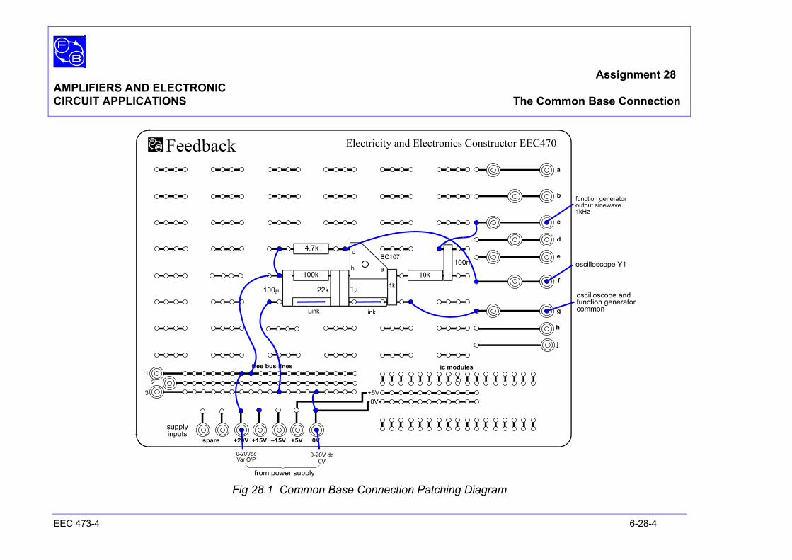
Assignment 28 AMPLIFIERS AND ELECTRONIC CIRCUIT APPLICATIONS The Common Base Connection
EEC 473-4 6-28-4
Fig 28.1 Common Base Connection Patching Diagram
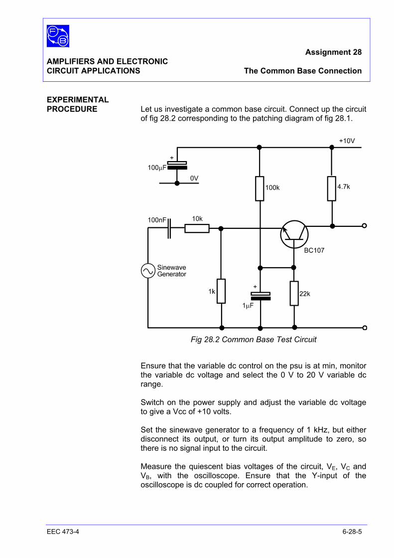
Assignment 28 AMPLIFIERS AND ELECTRONIC CIRCUIT APPLICATIONS The Common Base Connection
EEC 473-4 6-28-5
EXPERIMENTAL PROCEDURE Let us investigate a common base circuit. Connect up the circuit
of fig 28.2 corresponding to the patching diagram of fig 28.1.
Fig 28.2 Common Base Test Circuit
Ensure that the variable dc control on the psu is at min, monitor
the variable dc voltage and select the 0 V to 20 V variable dc range. Switch on the power supply and adjust the variable dc voltage to give a Vcc of +10 volts. Set the sinewave generator to a frequency of 1 kHz, but either disconnect its output, or turn its output amplitude to zero, so there is no signal input to the circuit. Measure the quiescent bias voltages of the circuit, VE, VC and VB, with the oscilloscope. Ensure that the Y-input of the oscilloscope is dc coupled for correct operation.
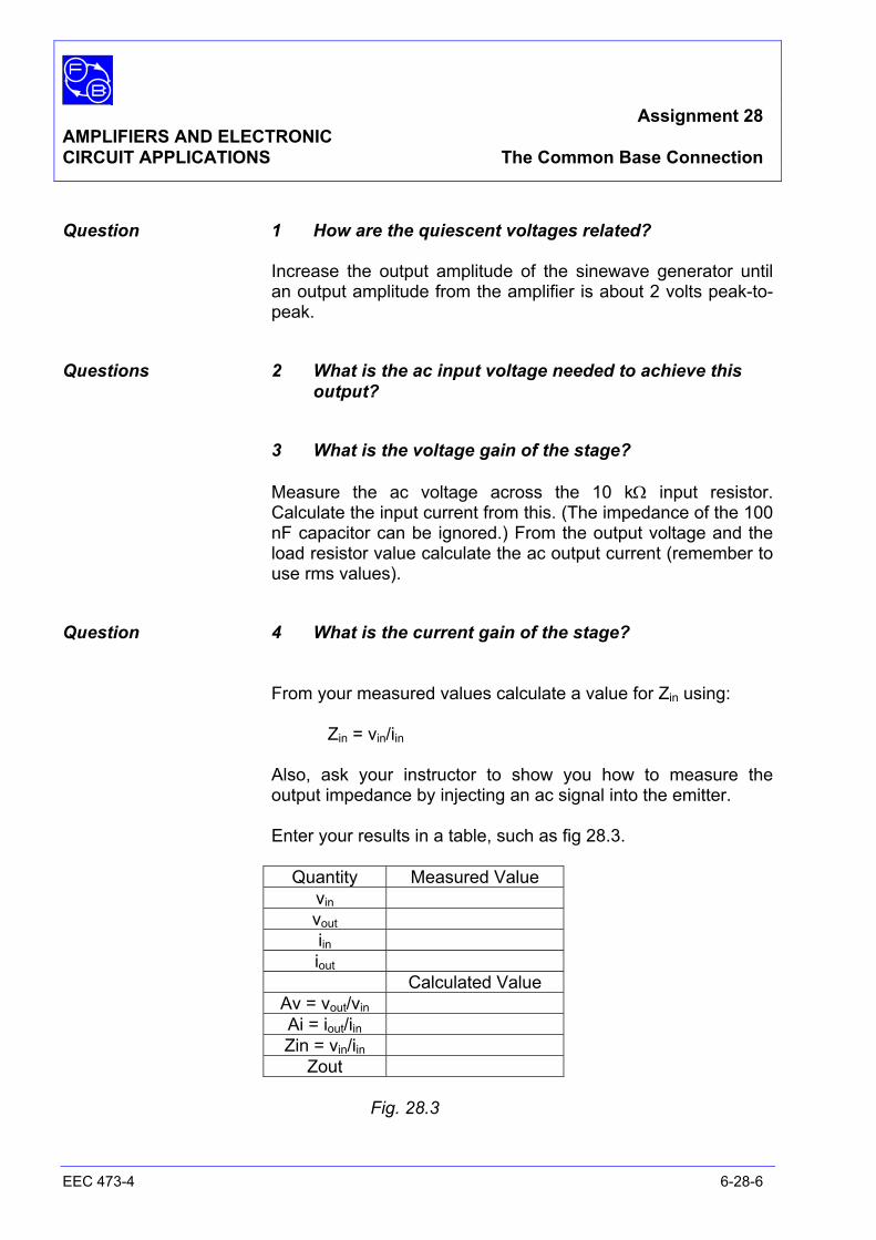
Assignment 28 AMPLIFIERS AND ELECTRONIC CIRCUIT APPLICATIONS The Common Base Connection
EEC 473-4 6-28-6
Question 1 How are the quiescent voltages related? Increase the output amplitude of the sinewave generator until an output amplitude from the amplifier is about 2 volts peak-to-peak.
Questions 2 What is the ac input voltage needed to achieve this output?
3 What is the voltage gain of the stage? Measure the ac voltage across the 10 kΩ input resistor. Calculate the input current from this. (The impedance of the 100 nF capacitor can be ignored.) From the output voltage and the load resistor value calculate the ac output current (remember to use rms values).
Question 4 What is the current gain of the stage? From your measured values calculate a value for Zin using:
Zin = vin/iin Also, ask your instructor to show you how to measure the output impedance by injecting an ac signal into the emitter. Enter your results in a table, such as fig 28.3.
Quantity Measured Value vin vout iin iout
Calculated Value Av = vout/vin Ai = iout/iin Zin = vin/iin
Zout Fig. 28.3
Assignment 28 AMPLIFIERS AND ELECTRONIC CIRCUIT APPLICATIONS The Common Base Connection
EEC 473-4 6-28-7
Question 5 How do the above parameters compare with those of a common emitter stage?
It should be seen that voltage gain for the common base connection is high, and is similar in magnitude as for the C.E stage. There is a phase reversal for the common base connection. Also the input resistance is very low compared with that for a C.E stage. The current gain however is very nearly unity. The output resistance is medium to high.
PRACTICAL CONSIDERATIONS AND APPLICATIONS The common base connected transistor is not the most used
connection.
The principle advantage at low frequencies of the common base circuit is the low input impedance. Such stages are useful for the input circuit of a current amplifier. Note that the succeeding stage cannot be another CB, as this would give a voltage gain (an thus power gain) of unity. The CB connection is more common in high frequency input circuits, where low impedances (typically 50 ohms) are encountered. Also, the stability of a CB stage is good at high frequencies.
Assignment 28 AMPLIFIERS AND ELECTRONIC CIRCUIT APPLICATIONS The Common Base Connection
EEC 473-4 6-28-8
Notes
Assignment 29 AMPLIFIERS AND ELECTRONIC CIRCUIT APPLICATIONS Multi-stage Amplifiers
EEC 473-4 6-29-1
OBJECTIVES 1 To familiarise the student with the concept of a multistage amplifier.
2 To provide an understanding of ac inter-stage coupling for a multistage amplifier.
EQUIPMENT REQUIRED Qty Apparatus
1 Electricity & Electronics Constructor EEC470
1 Amplifiers and Circuit Applications Kit EEC473-4
1 Power supply unit 0 to 20 V variable dc regulated. (eg, Feedback Power Supply 92-445 or Teknikit Console 92-100)
1 Oscilloscope, general purpose 20 MHz
1 Sinewave generator, 1 kHz
PREREQUISITE ASSIGNMENTS Basic Electricity and Electronics EEC471-2,
Assignment 34
KNOWLEDGE LEVEL Before working this assignment you should:
Know the operation of a common emitter transistor amplifier circuit.
Assignment 29 AMPLIFIERS AND ELECTRONIC CIRCUIT APPLICATIONS Multi-stage Amplifiers
EEC 473-4 6-29-2
Notes
Assignment 29 AMPLIFIERS AND ELECTRONIC CIRCUIT APPLICATIONS Multi-stage Amplifiers
EEC 473-4 6-29-3
INTRODUCTION Often it is impossible to achieve all the required gain from a single stage of amplification. For example, if an output voltage of 10 volts rms was required, and an input voltage of only 1mV was available, an amplifier with a voltage gain of 10,000 would be needed. This is normally too high a gain for a single stage to supply, therefore more than one stage is needed. Consider a stage A, with a gain A1 (it does not matter whether its voltage or current gain), connected to a second stage B, with a gain A2. This is shown in fig 29.1.
Fig 29.1 Suppose an input of (a) units is applied to stage A. The output from stage A will be (A1a) units. Thus (A1a) units are applied to stage B giving an output from B of [A2(A1a)] Thus the total gain of the two stages connected in series is given by:
AT = A1 x A2
The total gain of series connected stages is the product of the individual stage gains. Thus to get a gain of 10,000, two stages with gains of 100 could be used, or three stages with gains of 22, etc. Having ascertained how many stages we need, the next problem is how do we connect the stages together? Assuming we are going to use common emitter connected stages, then the collector of the first stage must be connected in some way to the base of the second stage. If the connection is made directly between the two stages, then the dc bias
Assignment 29 AMPLIFIERS AND ELECTRONIC CIRCUIT APPLICATIONS Multi-stage Amplifiers
EEC 473-4 6-29-4
conditions of the two stages will be upset, and they will not function properly. Thus some form of connection which allows the signal to pass, but allows no dc coupling, is required.
Question 1 What component will do this? This type of inter-stage coupling is known as capacitor coupling, or sometimes resistor-capacitor, or RC coupling. With capacitor coupled stages, each stage can be designed separately as far as dc bias conditions are concerned. However, the ac signal loading of one stage on the preceding one must be taken into account.
Assignment 29 AMPLIFIERS AND ELECTRONIC CIRCUIT APPLICATIONS Multi-stage Amplifiers
EEC 473-4 6-29-5
Notes
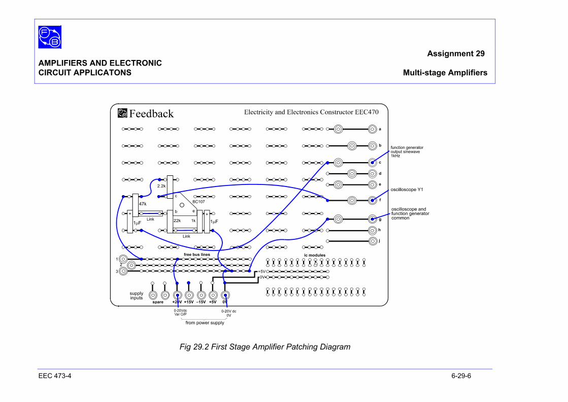
Assignment 29 AMPLIFIERS AND ELECTRONIC CIRCUIT APPLICATONS Multi-stage Amplifiers
EEC 473-4 6-29-6
Fig 29.2 First Stage Amplifier Patching Diagram
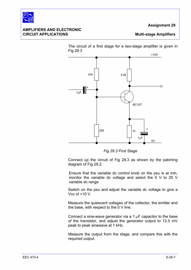
Assignment 29 AMPLIFIERS AND ELECTRONIC CIRCUIT APPLICATIONS Multi-stage Amplifiers
EEC 473-4 6-29-7
The circuit of a first stage for a two-stage amplifier is given in Fig 29.3
Fig 29.3 First Stage Connect up the circuit of Fig 29.3 as shown by the patching diagram of Fig 29.2.
Ensure that the variable dc control knob on the psu is at min, monitor the variable dc voltage and select the 0 V to 20 V variable dc range.
Switch on the psu and adjust the variable dc voltage to give a Vcc of +10 V. Measure the quiescent voltages of the collector, the emitter and the base, with respect to the 0 V line. Connect a sine-wave generator via a 1 µF capacitor to the base of the transistor, and adjust the generator output to 12.5 mV peak to peak sinewave at 1 kHz. Measure the output from the stage, and compare this with the required output.
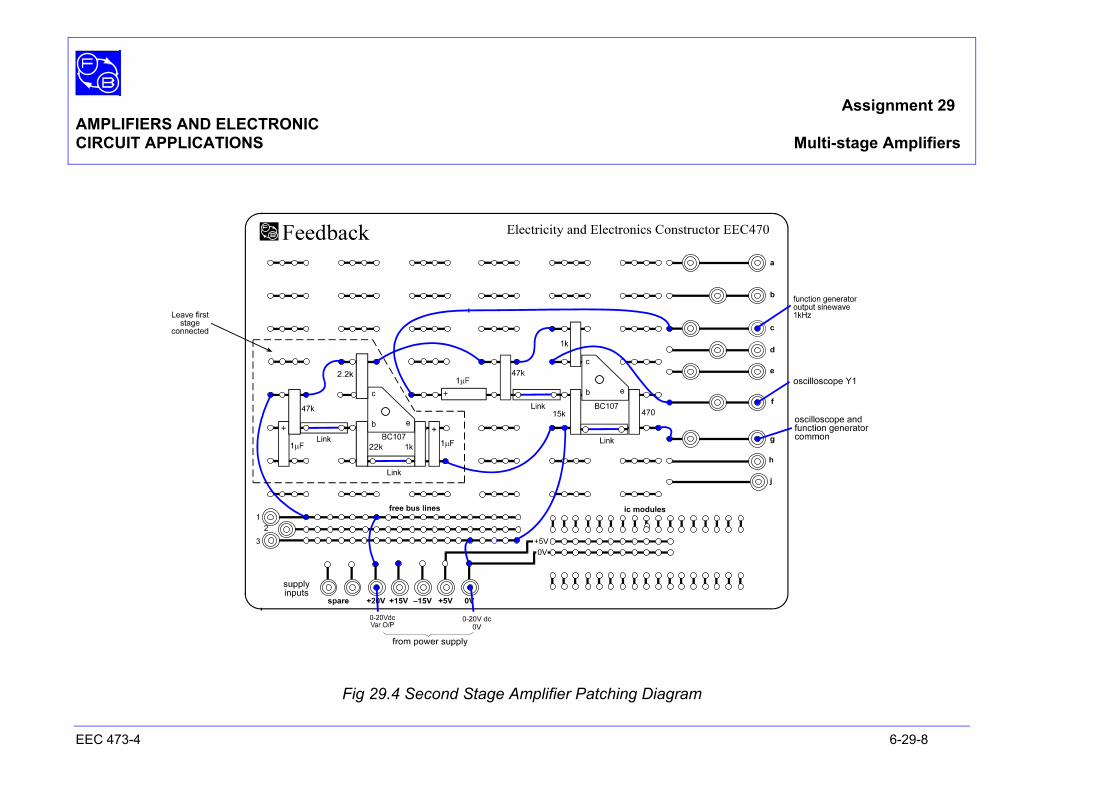
Assignment 29 AMPLIFIERS AND ELECTRONIC CIRCUIT APPLICATIONS Multi-stage Amplifiers
EEC 473-4 6-29-8
Fig 29.4 Second Stage Amplifier Patching Diagram
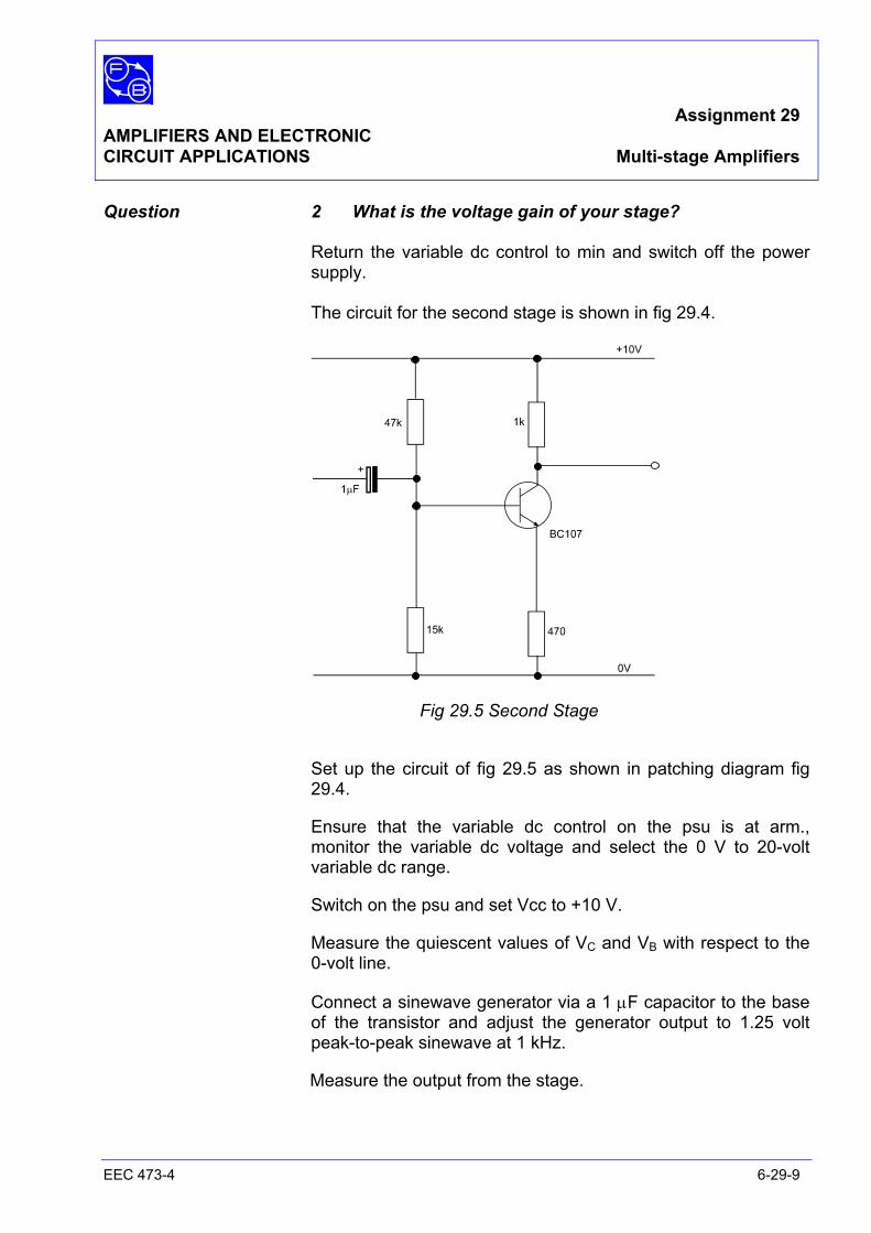
Assignment 29 AMPLIFIERS AND ELECTRONIC CIRCUIT APPLICATIONS Multi-stage Amplifiers
EEC 473-4 6-29-9
Question 2 What is the voltage gain of your stage? Return the variable dc control to min and switch off the power supply. The circuit for the second stage is shown in fig 29.4.
Fig 29.5 Second Stage
Set up the circuit of fig 29.5 as shown in patching diagram fig 29.4.
Ensure that the variable dc control on the psu is at arm., monitor the variable dc voltage and select the 0 V to 20-volt variable dc range.
Switch on the psu and set Vcc to +10 V.
Measure the quiescent values of VC and VB with respect to the 0-volt line.
Connect a sinewave generator via a 1 µF capacitor to the base of the transistor and adjust the generator output to 1.25 volt peak-to-peak sinewave at 1 kHz.
Measure the output from the stage.
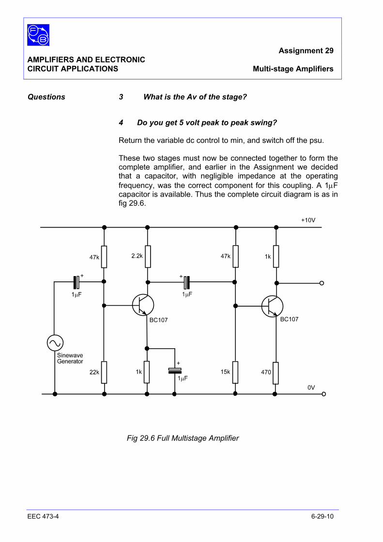
Assignment 29 AMPLIFIERS AND ELECTRONIC CIRCUIT APPLICATIONS Multi-stage Amplifiers
EEC 473-4 6-29-10
Questions 3 What is the Av of the stage?
4 Do you get 5 volt peak to peak swing? Return the variable dc control to min, and switch off the psu. These two stages must now be connected together to form the complete amplifier, and earlier in the Assignment we decided that a capacitor, with negligible impedance at the operating frequency, was the correct component for this coupling. A 1µF capacitor is available. Thus the complete circuit diagram is as in fig 29.6.
Fig 29.6 Full Multistage Amplifier

Assignment 29 AMPLIFIERS AND ELECTRONIC CIRCUIT APPLICATIONS Multi-stage Amplifiers
EEC 473-4 6-29-11
Notes
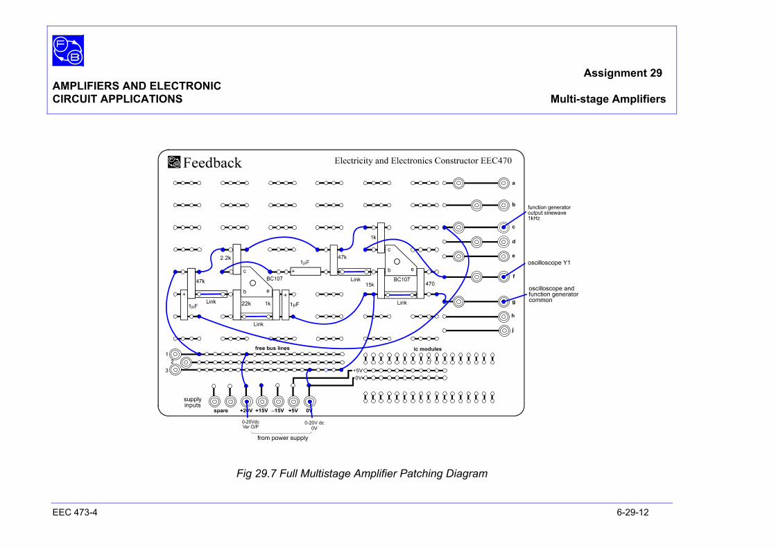
Assignment 29 AMPLIFIERS AND ELECTRONIC CIRCUIT APPLICATIONS Multi-stage Amplifiers
EEC 473-4 6-29-12
Fig 29.7 Full Multistage Amplifier Patching Diagram
Assignment 29 AMPLIFIERS AND ELECTRONIC CIRCUIT APPLICATIONS Multi-stage Amplifiers
EEC 473-4 6-29-13
Set up the total circuit as in fig 29.6 given by the module connection of fig 29.7. Ensure that the variable dc control is at min, monitor the variable dc voltage and select the 0 V to 20 volt variable dc range. Switch on the psu and set Vcc to 10 V. Adjust the sinewave generator output to 12.5 mV peak-to-peak sinewave at 1 kHz and measure the output from the stage.
Questions 5 What is the voltage gain of the two-stage amplifier?
6 How does this compare with the gain of the individual stages?
7 Can you explain why the gain observed is slightly different to the expected value?
8 Does the method of coupling between stages give satisfactory results?
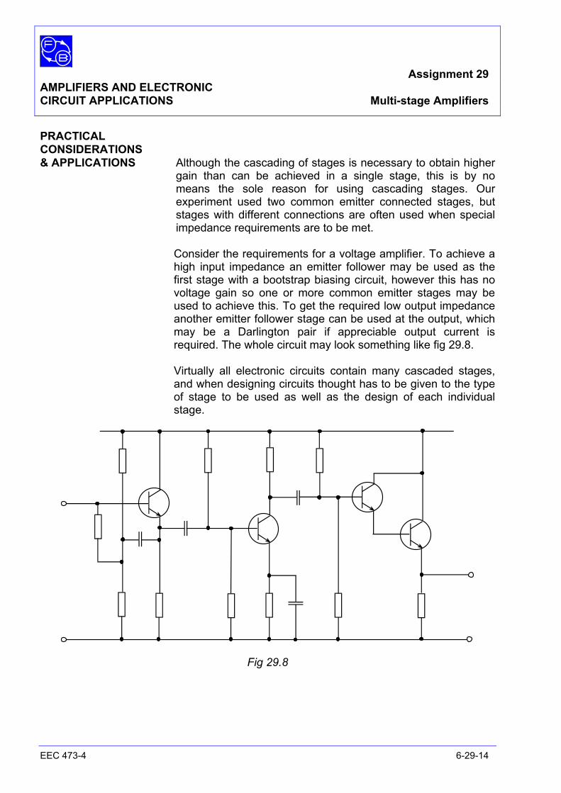
Assignment 29 AMPLIFIERS AND ELECTRONIC CIRCUIT APPLICATIONS Multi-stage Amplifiers
EEC 473-4 6-29-14
PRACTICAL CONSIDERATIONS & APPLICATIONS Although the cascading of stages is necessary to obtain higher
gain than can be achieved in a single stage, this is by no means the sole reason for using cascading stages. Our experiment used two common emitter connected stages, but stages with different connections are often used when special impedance requirements are to be met. Consider the requirements for a voltage amplifier. To achieve a high input impedance an emitter follower may be used as the first stage with a bootstrap biasing circuit, however this has no voltage gain so one or more common emitter stages may be used to achieve this. To get the required low output impedance another emitter follower stage can be used at the output, which may be a Darlington pair if appreciable output current is required. The whole circuit may look something like fig 29.8. Virtually all electronic circuits contain many cascaded stages, and when designing circuits thought has to be given to the type of stage to be used as well as the design of each individual stage.
Fig 29.8
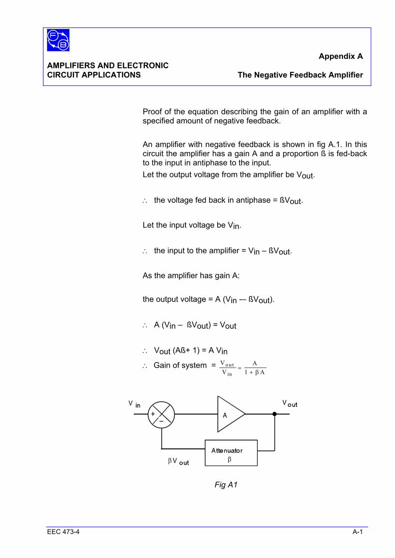
Appendix A AMPLIFIERS AND ELECTRONIC CIRCUIT APPLICATIONS The Negative Feedback Amplifier
EEC 473-4 A-1
Proof of the equation describing the gain of an amplifier with a
specified amount of negative feedback. An amplifier with negative feedback is shown in fig A.1. In this
circuit the amplifier has a gain A and a proportion ß is fed-back to the input in antiphase to the input.
Let the output voltage from the amplifier be Vout. ∴ the voltage fed back in antiphase = ßVout. Let the input voltage be Vin. ∴ the input to the amplifier = Vin – ßVout. As the amplifier has gain A: the output voltage = A (Vin -– ßVout). ∴ A (Vin – ßVout) = Vout ∴ Vout (Aß+ 1) = A Vin
∴ Gain of system = VV
AA
out
in=
+1 β
Fig A1
Appendix A AMPLIFIERS AND ELECTRONIC CIRCUIT APPLICATIONS The Negative Feedback Amplifier
EEC 473-4 A-2
Note that this assumes the amplifier to have a gain of + A; for an inverting amplifier such as an operational amplifier operating in the closed-loop mode the equation would be modified.
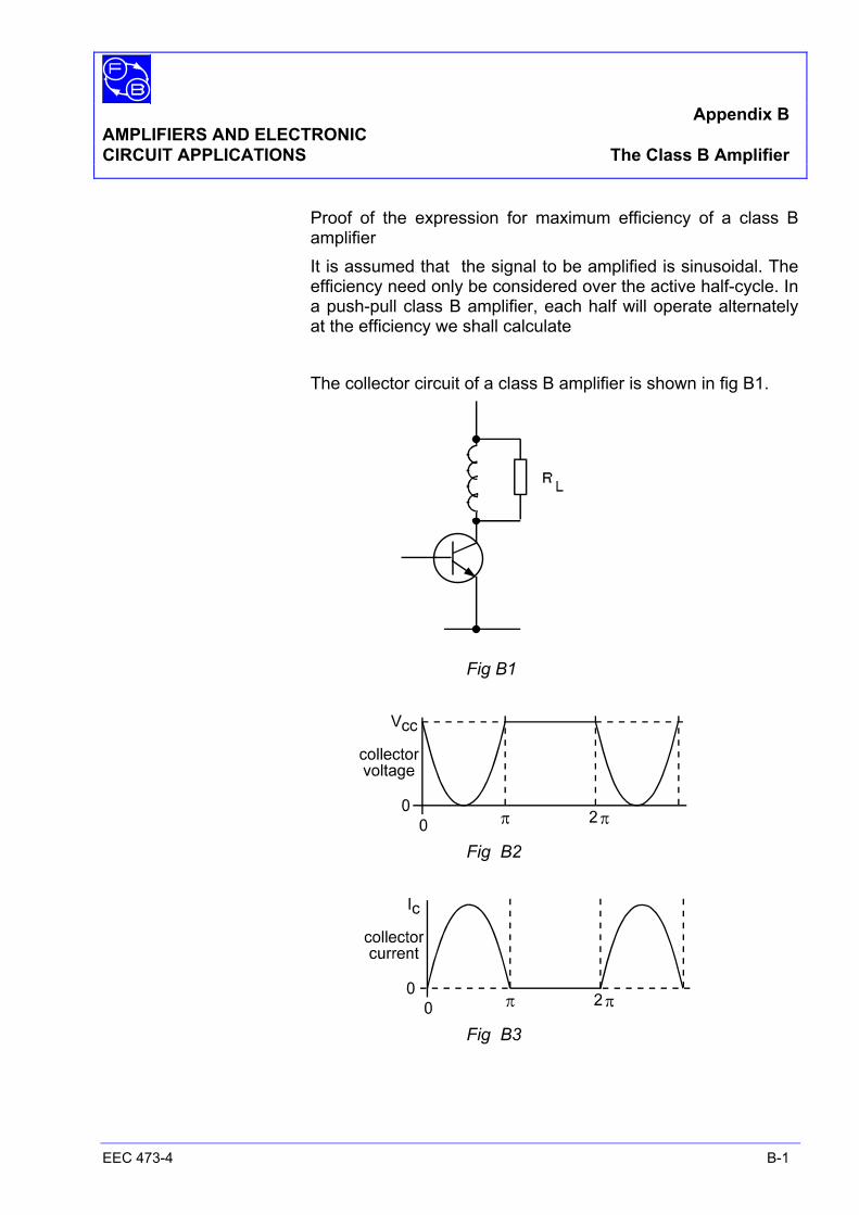
Appendix B AMPLIFIERS AND ELECTRONIC CIRCUIT APPLICATIONS The Class B Amplifier
EEC 473-4 B-1
Proof of the expression for maximum efficiency of a class B amplifier
It is assumed that the signal to be amplified is sinusoidal. The efficiency need only be considered over the active half-cycle. In a push-pull class B amplifier, each half will operate alternately at the efficiency we shall calculate
The collector circuit of a class B amplifier is shown in fig B1.
Fig B1
Fig B2
Fig B3
Appendix B AMPLIFIERS AND ELECTRONIC CIRCUIT APPLICATIONS The Class B Amplifier
EEC 473-4 B-2
Assuming that the full collector voltage swing is used as in fig
B2, drawing collector current as shown in fig B3 the power available in the load can be calculated thus:
collector voltage = Vcc (1 - sin x) load voltage = Vcc sin x
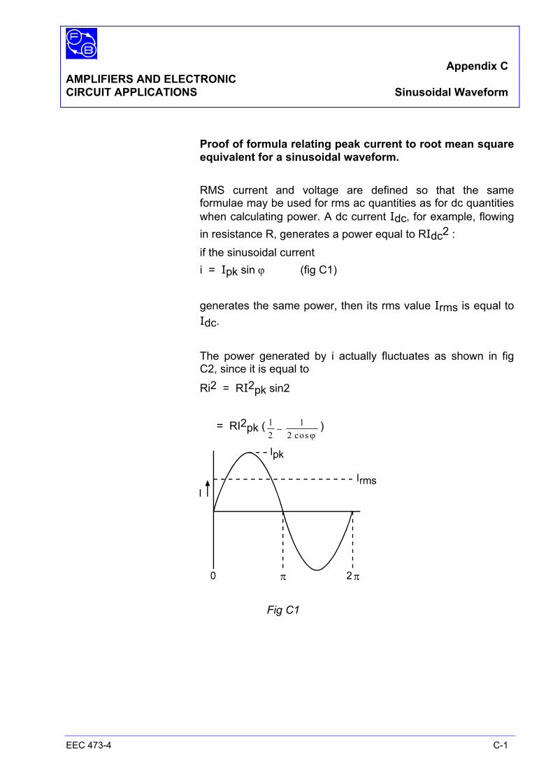
Appendix C AMPLIFIERS AND ELECTRONIC CIRCUIT APPLICATIONS Sinusoidal Waveform
EEC 473-4 C-1
Proof of formula relating peak current to root mean square
equivalent for a sinusoidal waveform. RMS current and voltage are defined so that the same
formulae may be used for rms ac quantities as for dc quantities when calculating power. A dc current Idc, for example, flowing in resistance R, generates a power equal to RIdc2 :
if the sinusoidal current i = Ipk sin ϕ (fig C1) generates the same power, then its rms value Irms is equal to
Idc. The power generated by i actually fluctuates as shown in fig
C2, since it is equal to
Ri2 = RI2pk sin2
= RI2pk ( 12
12
−cosϕ
)
Fig C1
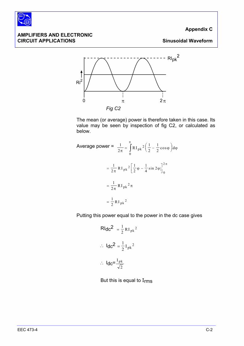
Appendix C AMPLIFIERS AND ELECTRONIC CIRCUIT APPLICATIONS Sinusoidal Waveform
EEC 473-4 C-2
Fig C2 The mean (or average) power is therefore taken in this case. Its
value may be seen by inspection of fig C2, or calculated as below.
Average power = 12
12
12
2
0π
ϕ ϕπ
= −
∫ RI dpk cos
= −
12
12
14
22
0
2
πϕ ϕ
πR I pk sin
=
12
2π
πRI pk
=
12
2R I pk
Putting this power equal to the power in the dc case gives RIdc2 =
12
2RI pk
∴ Idc2 =
12
2I pk
∴ Idc= I pk
2
But this is equal to Irms


