Embed Size (px)
Citation preview

A plasmonic antenna-coupledsuperconducting near-IR photon
detector
Faustin W. Carter,1,∗ Daniel F. Santavicca,2 and Daniel E. Prober1
1Yale University Applied Physics Department, 15 Prospect St., New Haven, CT 06511, USA2University of North Florida Physics Department, 1 UNF Dr., Jacksonville, FL 32224, USA
Abstract: The extremely small size of plasmonic antennas has made itdifficult to integrate them with nanoscale detectors that require electricalleads, as the leads tend to degrade the resonant properties of the antenna.We present a design for integrating a plasmonic antenna with a nanoscalesuperconducting transition-edge sensor (TES) with electrical leads. Nu-merical simulations demonstrate high-efficiency coupling of 1550 nmincident photons into the sub-wavelength TES. Although we have chosen todesign around a TES, this approach is broadly applicable to any dissipativenanoscale device that requires an electrical connection.
© 2014 Optical Society of America
OCIS codes: (250.0040) Detectors; (220.2740) Geometric optical design; (250.5403) Plas-monics; (310.6628) Subwavelength structures, nanostructures; (310.6860) Thin films, opticalproperties.
References and links1. G. Rebeiz, “Millimeter-wave and terahertz integrated circuit antennas,” Proc. IEEE 80, 1748–1770 (1992).2. L. Novotny and N. van Hulst, “Antennas for light,” Nat. Photonics 5, 83–90 (2011).3. P. Bharadwaj, B. Deutsch, and L. Novotny, “Optical antennas,” Adv. Opt. Photonics 1, 438–483 (2009).4. W. Zhang, L. Huang, C. Santschi, and O. J. F. Martin, “Trapping and sensing 10 nm metal nanoparticles using
plasmonic dipole antennas.” Nano Lett. 10, 1006–1011 (2010).5. M. W. Knight, H. Sobhani, P. Nordlander, and N. J. Halas, “Photodetection with active optical antennas.” Science
332, 702–704 (2011).6. L. Tang, S. E. Kocabas, S. Latif, A. K. Okyay, D.-S. Ly-Gagnon, K. C. Saraswat, and D. a. B. Miller, “Nanometre-
scale germanium photodetector enhanced by a near-infrared dipole antenna,” Nat. Photonics 2, 226–229 (2008).7. L. Novotny, “Effective wavelength scaling for optical antennas,” Phys. Rev. Lett. 98, 266802 (2007).8. E. S. Barnard, T. Coenen, E. J. R. Vesseur, A. Polman, and M. L. Brongersma, “Imaging the hidden modes of
ultrathin plasmonic strip antennas by cathodoluminescence.” Nano Lett. 11, 4265–4269 (2011).9. A. Alu and N. Engheta, “Theory, modeling and features of optical nanoantennas,” IEEE Trans. Antennas Propag.
61, 1508–1517 (2013).10. W. Zhang, H. Fischer, T. Schmid, R. Zenobi, and O. J. F. Martin, “Mode-selective surface-enhanced raman
spectroscopy using nanofabricated plasmonic dipole antennas,” J. Phys. Chem. C 113, 14672–14675 (2009).11. L. J. E. Anderson, E. Hansen, E. Y. Lukianova-Hleb, J. H. Hafner, and D. O. Lapotko, “Optically guided con-
trolled release from liposomes with tunable plasmonic nanobubbles.” J. Controlled Release 144, 151–158 (2010).12. A. G. Curto, G. Volpe, T. H. Taminiau, M. P. Kreuzer, R. Quidant, and N. F. van Hulst, “Unidirectional emission
of a quantum dot coupled to a nanoantenna.” Science 329, 930–933 (2010).13. R. W. Heeres, S. N. Dorenbos, B. Koene, G. S. Solomon, L. P. Kouwenhoven, and V. Zwiller, “On-chip single
plasmon detection.” Nano Lett. 10, 661–664 (2010).14. P. Fan, K. C. Y. Huang, L. Cao, and M. L. Brongersma, “Redesigning photodetector electrodes as an optical
antenna.” Nano Lett. 13, 392–396 (2013).15. K. Irwin and G. Hilton, “Transition-edge sensors,” in Cryogenic particle detection, of Topics in Applied Physics,
C. Enss, ed. (Springer Berlin Heidelberg, 2005), vol. 99, pp. 63–150.
#213044 - $15.00 USD Received 28 May 2014; revised 24 Aug 2014; accepted 26 Aug 2014; published 4 Sep 2014(C) 2014 OSA 8 September 2014 | Vol. 22, No. 18 | DOI:10.1364/OE.22.022062 | OPTICS EXPRESS 22062

16. A. Lita, A. Miller, and S. Nam, “Counting near-infrared single-photons with 95% efficiency,” Opt. Express 16,3032–3040 (2008).
17. B. S. Karasik, S. V. Pereverzev, A. Soibel, D. F. Santavicca, D. E. Prober, D. Olaya, and M. E. Gershenson,“Energy-resolved detection of single infrared photons with λ = 8 µm using a superconducting microbolometer,”Appl. Phys. Lett. 101, 052601 (2012).
18. D. E. Prober, “Superconducting terahertz mixer using a transition-edge microbolometer,” Appl. Phys. Lett. 62,2119–2121 (1993).
19. P. L. Richards, “Bolometers for infrared and millimeter waves,” J. Appl. Phys. 76, 1–24 (1994).20. D. F. Santavicca, F. W. Carter, and D. E. Prober, “Proposal for a ghz count rate near-ir single-photon detector
based on a nanoscale superconducting transition edge sensor,” Proc. SPIE 8033, 80330W (2011).21. C. Brewitt-Taylor, D. Gunton, and H. Rees, “Planar antennas on a dielectric surface,” Electron. Lett. 17, 729–731
(1981).
1. Introduction
Efficient coupling of radiation into a sub-wavelength detector using an antenna is well under-stood at radio and microwave frequencies. These techniques have been extended to the THzdomain by scaling down the antenna dimensions to the 100 µm range [1]. Unfortunately, thisproportional scaling down of the antenna size no longer works at frequencies well above theTHz. This is because metals no longer behave like good conductors near their plasma frequency(∼ 3.57× 10¹⁵ Hz for aluminum). Recent research has begun to provide a theoretical frame-work and establish design rules for so-called optical antennas [2,3]. These antennas operate bycoupling incident radiation to collective electron oscillation modes called surface plasmons.
One such design is the plasmonic dipole [4–9]; it is analogous to the common radio dipoleantenna, with two main differences. The first is that a radio dipole is designed to match thefree-space wavelength of the radio signal, while a plasmonic dipole is designed to match thewavelength of a surface plasmon that is created by the incident free space radiation. The secondis that plasmonic dipoles are much smaller than their radio and microwave counterparts, whichmakes attaching electrical leads (for reading out lower-frequency information such as rectifiedor mixed-down signals) problematic. The leads on a THz antenna can easily be made muchsmaller than the antenna in order not to disturb the antenna properties. However, plasmonicdipoles that resonate at optical frequencies (1014–1015 Hz) are only a few 10s to a few 100sof nanometers in size, making the fabrication of nonperturbative electrical leads a significantchallenge.
Because of their extremely small size and the difficulties inherent in fabricating leads, plas-monic antennas have been primarily utilized for measurements that do not require a directelectrical connection to the antenna. Examples include tip-enhanced Raman spectroscopy [10],attaching resonant nanoparticles to a macroscopic object in order to concentrate the field lo-cally [11], coupling the emission of a quantum dot with a nano-antenna [12], and using plas-monic dipole antennas to increase the polarization-dependent light collection of a large-scaledetector [5]. One notable exception is a paper by Tang et al. [6], where a germanium photodiodeis placed at the feed gap of a plasmonic dipole antenna. Electrical leads are oriented perpen-dicular to the antenna, but they are larger than the size of the antenna and hence their effectscannot be neglected. Another configuration that has been demonstrated is that of terminatinga plasmonic waveguide with a superconducting nanowire single-photon detector (SNSPD) tomeasure individual plasmons [13]. Although this is not an antenna (the detector is many timeslarger than the incident wavelength), it is a successful implementation of a plasmonic system de-livering energy to a superconducting detector. Finally, an example of using metal electrodes toenhance optical absorption in a semiconductor nanowire photodetector was recently describedby Fan et al. [14]
This paper presents a design for a plasmonic antenna that couples to a sub-wavelength de-tector while allowing a direct electrical connection to the detector — in our case, a supercon-
#213044 - $15.00 USD Received 28 May 2014; revised 24 Aug 2014; accepted 26 Aug 2014; published 4 Sep 2014(C) 2014 OSA 8 September 2014 | Vol. 22, No. 18 | DOI:10.1364/OE.22.022062 | OPTICS EXPRESS 22063

ducting transition edge sensor (TES). The TES exploits the temperature-dependent resistance ofthe superconducting phase transition to detect the energy of an absorbed photon [15]. The TESis biased and its resistance is monitored using electrical leads. Our design allows for the imple-mentation of electrical leads that are simple to fabricate and do not compromise the plasmonicenhancement effects of the antenna. This design is broadly applicable to the integration of aplasmonic antenna with any dissipative nanoscale detector that requires an electrical readout.
The superconducting TES is the most sensitive energy-resolving single-photon detectordemonstrated to date, with single-photon sensitivity into the near- and mid-IR [16, 17]. Theintrinsic energy resolution (δE) of a superconducting TES scales as δE ≈
√T 3A, where T is
temperature and A is device area. Thus, antenna coupling allows one to use a much smallerTES area compared to what is possible with regular optical coupling (where the device areais on the order of a few λ 2). Reducing the device size allows one to operate at a much highertemperature for a given δE. Recent work on TES detectors [16] for detecting near-IR photonsused regular optical coupling, with TES area A = 1600 µm2, which can be compared to thearea of the niobium (Nb) TES of Fig. 1, with A = 0.065 µm2. The sub-wavelength TES alsoallows for diffusion cooling, which achieves a much faster detector response [18] and hence alarger photon counting rate.
Efficient antenna-coupling to a sub-wavelength TES is well-established at THz frequen-cies [19], but has not been demonstrated at near-IR or optical frequencies. A calculation of thesensitivity, speed, and saturation threshold of a nanoscale TES has been done by Santavicca etal. for near-IR detection [20]. For a niobium detector element that is 325 nm long, 200 nm wide,and 16 nm thick with a superconducting critical temperature Tc = 5 K, the predicted responsetime is 107 ps and the predicted intrinsic RMS energy resolution is 0.44 eV. Here we present ascheme for achieving efficient coupling of 1550 nm near-IR photons to such a nanoscale TES.
2. Antenna design
2.1. Discussion
The traditional method for attaching a radio dipole antenna to a much smaller detector (a diode,for instance) is to place the detector at the small feed gap between two quarter-wavelengthstrips (or rods). This configuration results in a half-wavelength resonator with the detector atthe current maximum. Optimal photon coupling is achieved when the antenna beam patternefficiently couples to the input photon beam; if one uses very narrow leads to read out thelower frequency signal from the detector, the antenna characteristics will not be significantlyperturbed. Unfortunately, this approach is not practical in the optical and near-IR regime dueto fabrication challenges — the feed gap and lead widths would necessarily be on the orderof a few tens of nanometers for an optical antenna. However, the basic idea of this design(detector at the central current maximum with leads designed to be non-perturbing at the inputfrequency) may be used to design a plasmonic version with one caveat: plasmonic systems usedisplacement current rather than current, and the input wavelength specified is that of a surfaceplasmon (λp) excited by the incident radiation rather than the free-space wavelength of theincident radiation itself (λ ). For simplicity of discussion, the terms current and wavelength willcontinue to be used, but when they are applied to the plasmonic system it is the displacementcurrent and plasmon wavelength that are being referred to.
For very small geometries it is advantageous from a fabrication standpoint to attach leadsto the ends of the plasmonic dipole antenna, rather than at the center. Large-area leads placedat the ends function as a high-frequency ground, forcing the ends of the dipole antenna to bevoltage nodes (current maxima). In order to place the detector at the center of the configura-tion and still have it at the point of maximum current, the half-wave dipole antenna must belengthened in to a full-wave resonator by extending its length to nλp where n is an integer.
#213044 - $15.00 USD Received 28 May 2014; revised 24 Aug 2014; accepted 26 Aug 2014; published 4 Sep 2014(C) 2014 OSA 8 September 2014 | Vol. 22, No. 18 | DOI:10.1364/OE.22.022062 | OPTICS EXPRESS 22064

In order to get the maximum voltage drop across the detector (thereby producing a large sig-nal), the dissipative/non-linear portion of the detector should be half a wavelength long andextensions (made of the same metal as the large leads) should be added on either end of thedissipative/non-linear section to make the total length nλp. In simulations we have discoveredthat it is actually advantageous to choose n = 2 rather than n = 1 as it increases the couplingefficiency (discussed later). Figure 1 shows our design, which uses aluminum (Al) for the ex-tensions and niobium (Nb) for the superconducting TES. The Al arms are thicker than the NbTES to promote good step-coverage during fabrication. The ground pads are much thicker thanthe Al arms to force a voltage node (or zero electric field) at the interface between the Al armsand the ground pads. The total combined length of the structure between the large leads is 2λp(or, more properly, 3λ Al
p /2+λ Nbp /2). The plasmon wavelength is longer in Al than it is in Nb,
which is why each 3λp/4 Al extension is more than 1.5 times larger than the λp/2 Nb section.
-400
-200
0
200
400
y po
sitio
n (n
m)
-1000 -500 0 500 1000x position (nm)
Nb AlAl
Semi-infinite ground/contanct pad
λp = Plasmon Wavelength
3λp/4 3λp/4λp/2
Fig. 1: Design for a TES coupled to a plasmonic resonator for 1550 nm photons. The totallength of the resonator is twice the plasmon wavelength. The dashed lines indicate the Nb/Aloverlap region, which is 50 nm long. The Nb element is 325 nm long, the Al elements are each680 nm long.
2.2. Calculation
The length of a plasmonic dipole antenna does not scale linearly with the incident free-spacephoton wavelength. Instead, the relationship between the incident free-space wavelength (λ )and the resulting plasmon wavelength (λp) must be determined for each material at each inci-dent wavelength. A theoretical treatment of the plasmonic dipole along with simplified antennascaling rules has been developed by Novotny [7], and an alternate formulation exists by Barnardet al. [8]. A discussion of the theory behind the loading of plasmonic dipole antennas with var-ious nano-loads is presented by Alu and Engheta [9]. A brief summary of the Novotny method(which we have used) follows: to begin, assume an infinitely long cylinder of radius R consist-ing of a metal embedded in a lossless dielectric with dielectric constant εs and wavenumberks =
√εsk0 where k0 = 2π/λ . Let z be the direction of the rod axis. At near-IR and optical
frequencies this metal rod will have a complex dielectric constant ε(λ ) with a negative realpart (kinetic inductance) and a positive imaginary part (dissipation). If this rod is illuminatedby radiation of wavelength λ polarized along its axis, one may deduce the modes that propa-gate down the rod in the z-direction by treating the rod as a waveguide and solving Maxwell’sEquations The solution may be obtained by using separation of variables: the radial part of themodes in the rod are given by the cylindrical Bessel functions Jn(κ1R), while the free-spacefields are defined by cylindrical Hankel functions of the first kind H(1)
n (κ2R). The longitudinalpart of the modes is sinusoidal and proportional to sin(2πz/λp), where λp depends on κ1 and
#213044 - $15.00 USD Received 28 May 2014; revised 24 Aug 2014; accepted 26 Aug 2014; published 4 Sep 2014(C) 2014 OSA 8 September 2014 | Vol. 22, No. 18 | DOI:10.1364/OE.22.022062 | OPTICS EXPRESS 22065
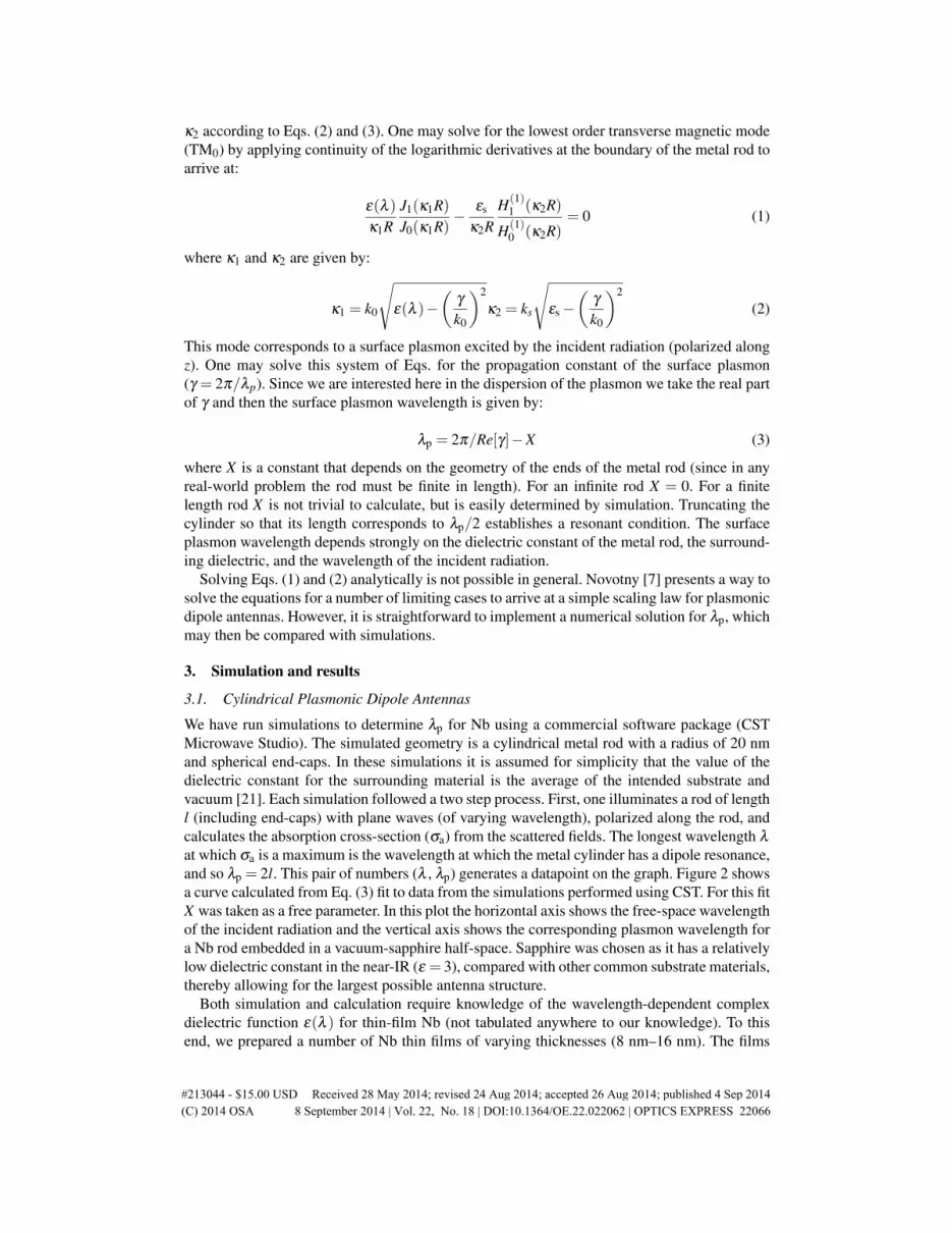
κ2 according to Eqs. (2) and (3). One may solve for the lowest order transverse magnetic mode(TM0) by applying continuity of the logarithmic derivatives at the boundary of the metal rod toarrive at:
ε(λ )
κ1RJ1(κ1R)J0(κ1R)
− εs
κ2RH(1)
1 (κ2R)
H(1)0 (κ2R)
= 0 (1)
where κ1 and κ2 are given by:
κ1 = k0
√ε(λ )−
(γ
k0
)2
κ2 = ks
√εs−
(γ
k0
)2
(2)
This mode corresponds to a surface plasmon excited by the incident radiation (polarized alongz). One may solve this system of Eqs. for the propagation constant of the surface plasmon(γ = 2π/λp). Since we are interested here in the dispersion of the plasmon we take the real partof γ and then the surface plasmon wavelength is given by:
λp = 2π/Re[γ]−X (3)
where X is a constant that depends on the geometry of the ends of the metal rod (since in anyreal-world problem the rod must be finite in length). For an infinite rod X = 0. For a finitelength rod X is not trivial to calculate, but is easily determined by simulation. Truncating thecylinder so that its length corresponds to λp/2 establishes a resonant condition. The surfaceplasmon wavelength depends strongly on the dielectric constant of the metal rod, the surround-ing dielectric, and the wavelength of the incident radiation.
Solving Eqs. (1) and (2) analytically is not possible in general. Novotny [7] presents a way tosolve the equations for a number of limiting cases to arrive at a simple scaling law for plasmonicdipole antennas. However, it is straightforward to implement a numerical solution for λp, whichmay then be compared with simulations.
3. Simulation and results
3.1. Cylindrical Plasmonic Dipole Antennas
We have run simulations to determine λp for Nb using a commercial software package (CSTMicrowave Studio). The simulated geometry is a cylindrical metal rod with a radius of 20 nmand spherical end-caps. In these simulations it is assumed for simplicity that the value of thedielectric constant for the surrounding material is the average of the intended substrate andvacuum [21]. Each simulation followed a two step process. First, one illuminates a rod of lengthl (including end-caps) with plane waves (of varying wavelength), polarized along the rod, andcalculates the absorption cross-section (σa) from the scattered fields. The longest wavelength λ
at which σa is a maximum is the wavelength at which the metal cylinder has a dipole resonance,and so λp = 2l. This pair of numbers (λ , λp) generates a datapoint on the graph. Figure 2 showsa curve calculated from Eq. (3) fit to data from the simulations performed using CST. For this fitX was taken as a free parameter. In this plot the horizontal axis shows the free-space wavelengthof the incident radiation and the vertical axis shows the corresponding plasmon wavelength fora Nb rod embedded in a vacuum-sapphire half-space. Sapphire was chosen as it has a relativelylow dielectric constant in the near-IR (ε = 3), compared with other common substrate materials,thereby allowing for the largest possible antenna structure.
Both simulation and calculation require knowledge of the wavelength-dependent complexdielectric function ε(λ ) for thin-film Nb (not tabulated anywhere to our knowledge). To thisend, we prepared a number of Nb thin films of varying thicknesses (8 nm–16 nm). The films
#213044 - $15.00 USD Received 28 May 2014; revised 24 Aug 2014; accepted 26 Aug 2014; published 4 Sep 2014(C) 2014 OSA 8 September 2014 | Vol. 22, No. 18 | DOI:10.1364/OE.22.022062 | OPTICS EXPRESS 22066

800
700
600
500
400
Plas
mon
wav
elen
gth
(nm
)
1600150014001300120011001000Incident wavelength (nm)
Theoretical Fit (one free parameter) CST simulations
Fig. 2: Calculation of λp from Eq. (3) for cylindrical Nb nano rods with R= 20 nm and differentlengths (solid line) has been fit to the results of CST simulations on the same geometry (opencircles) with one free parameter (X = 198 nm). Inset depicts simulation geometry. Dashed linesindicate λp at 1550 nm.
were fabricated via electron-beam deposition of Nb onto room-temperature sapphire substrates.They were then sent to J.A. Woollam Co. where the complex index of refraction n(λ )+ ik(λ )was measured via spectroscopic ellipsometry for each Nb thickness; ε(λ ) was then computedfrom n(λ ) and k(λ ). Figure 3 shows the n and k data from J.A. Woolam for a Nb thickness of16 nm. This thickness has a superconducting critical temperature (Tc) of approximately 7 K.The optical parameters of the other thickness films were qualitatively similar in shape, anddiffered by up to 10% in n and 20% in k at λ = 1500 nm.
8
7
6
5
4
3
2
1
Inde
x of
refra
ctio
n
1600140012001000800600400200Wavelength (nm)
n k
Fig. 3: Wavelength-dependent complex index of refraction for 16 nm thick Nb film.
We repeated this simulation for Al using book values for ε(λ ) of Al, but do not include
#213044 - $15.00 USD Received 28 May 2014; revised 24 Aug 2014; accepted 26 Aug 2014; published 4 Sep 2014(C) 2014 OSA 8 September 2014 | Vol. 22, No. 18 | DOI:10.1364/OE.22.022062 | OPTICS EXPRESS 22067

those results as they closely match those of Novotny [7]. A final caveat is that any real-worldthin-film device will consist of a planar nanowire with a rectangular, rather than cylindrical,cross-section. Despite this difference, the analysis presented above works well for a planarnanowire provided one chooses an appropriate effective radius to plug into the calculation. Theeffective radius depends on the cross-sectional area of the nano-wire.
3.2. Full antenna-coupled detector design
1450
1400
1350
1300
1250
Tota
l Al l
engt
h (n
m)
350300250200150
Nb element length (nm)
10-5 10-4 10-3 10-2 10-1 100Normalized power absorbed in Nb
Nb + Al length = 2λp Initial point from cylindrical
calculations (R = 20 nm)
Fig. 4: Power absorbed in Nb detector (normalized to 1) as a function of both Al and Nb length,for λ = 1550 nm. The superimposed black line is a best fit to Eq. 4. The small cross indicatesthe initial parameters from the calculation of λp for Nb and Al cylinders with radii of 20 nm.
The results in Fig. 2 (and a similar calculation for Al) were used as initial parameters fordetermining the optimal length of the Nb and Al components of the design depicted in Fig. 1.We then performed a parametric analysis in Ansoft HFSS, a commercial high-frequency EMsolver package. The Nb element is modeled as 16 nm thick, the Al extensions are 66 nm thick,and the large ground pads (the two leads) are 200 nm thick. The substrate is sapphire (rather,the surrounding dielectric is an average of vacuum and sapphire as in the previous section). Theleft, right, top, and bottom borders of the cell have periodic boundary conditions, and the twosurfaces parallel to the page have what is called a radiation boundary; the program attempts toballoon them out to infinity. The bounding box was sized large enough that the periodic spacingof the antennas was sufficient to avoid any coupling between antennas. The Nb and Al lengthswere treated as independent parameters. The simulation engine illuminated the structure witha 1550 nm plane wave polarized along the detector length and computed the power absorbedin the Nb element by integrating the Poynting vector ~S = (~Ei +~Es)× (~Hi + ~Hs) (where “i” and“s” denote incident and scattered) over all surfaces of the Nb element. This was repeated for
#213044 - $15.00 USD Received 28 May 2014; revised 24 Aug 2014; accepted 26 Aug 2014; published 4 Sep 2014(C) 2014 OSA 8 September 2014 | Vol. 22, No. 18 | DOI:10.1364/OE.22.022062 | OPTICS EXPRESS 22068

a range of different Nb and Al lengths. The results of this parametric analysis are depicted inFig. 4, where the x-axis is Nb length (lNb), the y-axis is Al length (lAl), and the color of thepoints indicates the (normalized) power absorbed in the Nb detector element.
The dashed black line in Fig. 4 is a fit to:
lNb
λ Nbp
+lAl
λ Alp
= 2 (4)
where the fit parameters λ Nbp and λ Al
p were calculated by assuming the maximum responsecorresponds to half of a plasmon wavelength in Nb, and three-quarters of a plasmon wavelengthin each Al section (see Figs. 1 and 6). Equation (4) is predicated on the assumption that forany given Nb (or Al) length, the maximum response occurs when the total structure lengthis equal to two plasmon wavelengths. This naive model qualitatively matches the simulatedresponse, however, the small deviation of the 2λp line at longer Nb lengths indicates that amore complicated model is needed to fully explain the antenna response. The small cross inFig. 4 indicates the starting point which was a result of calculations for a cylinder with a radiusof 20 nm. This is remarkably close to the optimal value for the rectangular cross section (within5%) and indicates that the cylindrical model is an excellent first approximation.
101
102
103
104
Pow
er e
nhan
cem
ent
160015801560154015201500Incident wavelength (nm)
Ratio of x to y polarization
Absolute power enhancement
Fig. 5: Red: power absorbed in Nb element due to incident light polarized along the axis of thedetector (x) normalized by power absorbed due to incident light polarized perpendicular to thedetector axis (y). Blue: power absorbed in Nb element with aluminum antenna/leads normalizedby power absorbed without any aluminum at all. Incident wavelength is free-space wavelength.See Fig. 1 for device design.
Figure 5 shows the simulated device response as a function of incident wavelength (computedby HFSS) for the optimal geometry as determined from Fig. 4 (lNb = 325 nm, lAl = 1360 nm).The vertical axis is the ratio of power absorbed by the detector, normalized in two differentways. The top curve (red) is the ratio of power absorbed by the detector from light polarizedparallel to the detector to power absorbed from light polarized perpendicular to the detector.The bottom curve (blue) is the absolute power enhancement; it is the ratio of power absorbedin the Nb with and without the Al antenna and ground pads. It is possible to tune the antenna
#213044 - $15.00 USD Received 28 May 2014; revised 24 Aug 2014; accepted 26 Aug 2014; published 4 Sep 2014(C) 2014 OSA 8 September 2014 | Vol. 22, No. 18 | DOI:10.1364/OE.22.022062 | OPTICS EXPRESS 22069

-400
-200
0
200
400
y po
sitio
n (n
m)
-1000 -500 0 500 1000x position (nm)
0 400 800 1200 1600Magnitude of field (V/m)
(a) Field Magnitude
-400
-200
0
200
400
y po
sitio
n (n
m)
-1000 -500 0 500 1000x position (nm)
-100 -50 0 50 100Z-component of field (V/m)
(b) Z-Component
Fig. 6: (a) Electric field strength at a height of 8 nm above the substrate (half the Nb height) su-perimposed on detector design (see Fig. 1) during illumination by 1550nm plane wave with fieldstrength of 1 V/m. Note the strong field concentration at the detector, and the two-wavelengthresonance (half a wavelength in the Nb, and three-halves in the Al). Also note the shorter plas-mon wavelength in the Nb vs. the Al. (b) Z-component of field in same plane showing anunambiguous two-wavelength resonance.
to different wavelengths by rescaling all the dimensions according to the calculations above.The sensitivity of the resonance to variations in length can be seen from Fig. 4 and is withinthe accuracy limits of commercial electron-beam lithography technology. Further broadeningof the peak is to be expected in any real-world implementation due to imperfections in thefabrication process, non-zero surface roughness, and possible defects in the thin films, whichmeans the detector should still operate well at the designed wavelength with small fabricationerrors.
Figure 6 depicts the electric field strength distribution at the resonance from Fig. 5 superim-posed over the device. The resulting electric field is concentrated in and around the Nb detectorelement; it is roughly two orders of magnitude stronger in the Nb than in the Al. One can clearly
#213044 - $15.00 USD Received 28 May 2014; revised 24 Aug 2014; accepted 26 Aug 2014; published 4 Sep 2014(C) 2014 OSA 8 September 2014 | Vol. 22, No. 18 | DOI:10.1364/OE.22.022062 | OPTICS EXPRESS 22070

see the plasmon wavelength distribution (longer in the Al by a factor of about two), and counttwo full wavelengths. It is worth noting that because the plasmon wavelength is much shorterthan the free-space photon wavelength, our 2λp design results in a device which is roughly1.7 µm long and so nearly the same size as the photon it is designed to detect. Our simulationshave shown much better coupling with the 2λp design compared to a resonator that is only oneplasmon wavelength long between the ground pads. We believe this is because the large groundpads of the smaller device serve to reflect more of the incident free-space photons, whereaswith the larger 2λp design, the gap between the pads is large enough to admit the photon to thedevice. This effect is one possible reason for the deviation of the response in Fig. 4 from thedashed line at smaller Al lengths.
4. Conclusions
We have developed an approach that allows integration of plasmonic antennas with nanoscaledevices that require an electrical connection. Our design is tunable (through fabrication) andstraightforward to fabricate using conventional electron beam lithography. The design’s mainadvantage is that the leads do not negatively perturb the antenna resonance. A secondary ad-vantage is that is naturally polarization sensitive. We demonstrate in our simulations that thisapproach should work well with a superconducting TES. In principle, this design could be ex-tended to any small detector that requires an electrical connection, for example, a photodiode.As long as the antenna material (Al in our case) experiences much less dissipation than thedetector (Nb in our case) at the resonant frequency, the power should couple strongly into thedetector element.
Acknowledgments
The authors thank Prof. Nader Engheta for helpful conversations, and Dr. Mike Rooks and Dr.Luigi Frunzio for their advice on device fabrication methods and tolerances. D.S. acknowl-edges support from the National Aeronautics and Space Administration through the Universityof Central Florida’s NASA Florida Space Grant Consortium (NNX10AM01H). F.C. acknowl-edges support from the NASA Connecticut Space Grant Consortium (NNX06AC32H). D.P.acknowledges support from the National Science Foundation (NSF) through the NSF-DMR-0907082 grant, and support from Yale University.
#213044 - $15.00 USD Received 28 May 2014; revised 24 Aug 2014; accepted 26 Aug 2014; published 4 Sep 2014(C) 2014 OSA 8 September 2014 | Vol. 22, No. 18 | DOI:10.1364/OE.22.022062 | OPTICS EXPRESS 22071


