Embed Size (px)
Citation preview
Silicon heterojunction solar cells
obtained by Hot-Wire CVD
Delfina Muñoz Cervantes
Director: Cristóbal Voz Sánchez
Memòria presentada per a l’obtenció del títol de Doctor
Barcelona, juliol de 2008


A mi padre, mi madre, Andrés y la Mari
"Would you tell me, please, which way I ought to go from here?" "That depends a good deal on where you want to get to," said the Cat. "I don't much care where –" said Alice. "Then it doesn't matter which way you go," said the Cat. "– so long as I get somewhere," Alice added as an explanation. "Oh, you're sure to do that," said the Cat, "if you only walk long enough."
L. Carroll, Alice's Adventures in Wonderland
“¿podrías decirme, por favor, qué camino debo seguir para salir de aquí?” “Esto depende en gran parte del sitio al que quieras llegar” dijo el Gato. “No me importa mucho el sitio...” dijo Alicia. “Entonces tampoco importa mucho el camino que tomes,” dijo el Gato. “...siempre que llegue a alguna parte” añadió Alicia como explicación. “¡Oh, siempre llegarás a alguna parte,” aseguró el Gato, “si caminas lo suficiente!”
L Carroll, Alicia en el Pais de las Maravillas

- 1 -
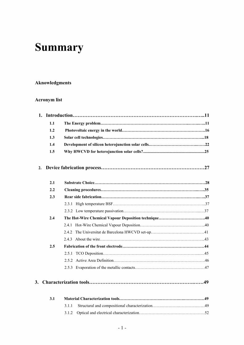
Summary
Aknowledgments
Acronym list
1. Introduction………………………………………………………………….…..11
1.1 The Energy problem………………………………………………………..……..…..11
1.2 Photovoltaic energy in the world…………………………………………………….16
1.3 Solar cell technologies………………………………………………………………...18
1.4 Development of silicon heterojunction solar cells.……………………………..……22
1.5 Why HWCVD for heterojunction solar cells?............................................................25
2. Device fabrication process………………………………………………………27
2.1 Substrate Choice………………………………………………………………………28
2.2 Cleaning procedures……………………………………………………………...…..35
2.3 Rear side fabrication……………………………………………………….……..…..37
2.3.1 High temperature BSF…………………………………………………………..37
2.3.2 Low temperature passivation………………………………………………...…37
2.4 The Hot-Wire Chemical Vapour Deposition technique…………………………….40
2.4.1 Hot-Wire Chemical Vapour Deposition………………………………….……..40
2.4.2 The Universitat de Barcelona HWCVD set-up…………………………………41
2.4.3 About the wire…………………………………………………………………..43
2.5 Fabrication of the front electrode……………………………………………………44
2.5.1 TCO Deposition……………………………………………………………..….45
2.5.2 Active Area Definition………………………………………………………….46
2.5.3 Evaporation of the metallic contacts……………………………………………47
3. Characterization tools……………………………………………………….……49
3.1 Material Characterization tools………………………….………….….……………49
3.1.1 Structural and compositional characterization…….………….………….……49
3.1.2 Optical and electrical characterization…………………………………………52
- 2 -
3.2 Characterization of solar cell precursors………………………………………….53
3.2.1 Spectroscopic Phase Modulated Ellipsometry in the UV-visible……………..53
3.2.2 The QSSPC technique………………………………………………………...58
3.3 Characterization of complete solar cells…………………………………………….…….63
3.3.1 Current – Voltage characteristics………………………………………….….63
3.3.2 Spectral Response……………………………………………………….……66
4. Amorphous and microcrystalline silicon deposited by HWCVD………………68
4.1 Between a-Si:H and µc-Si:H…………………………………………………….……68
4.2 Device-quality intrinsic amorphous silicon deposited by HWCVD…………….…..70
4.3 Doped amorphous & microcrystalline silicon deposited by HWCVD………..……76
5. Precursor fabrication & characterization……………………………….………84
5.1 Characterization of HWCVD heterojunction emitters on p-type wafers…………….85
5.1.1 Band diagram of the heterojunction emitter………………………………….85
5.1.2 Limits to the open-circuit voltage…………………………..…….…………..86
5.1.3 Influence of the intrinsic buffer layer………………………….…………..….91
5.1.4 Influence of pre-treatments at the a-Si:H/c-Si interface………………………95
5.1.5 Influence of post-treatments after a-Si:H deposition…………………..……...97
5.1.6 Influence of the n-doped layer………………………………….………..……98
5.2 Characterization of BSF contacts deposited by HWCVD on p-type wafers...…..…100
5.2.1 Band diagram of the (p+)a-Si:H/(p)c-Si structure……………………...……100
5.2.2 Optimization of the p-doped layer ………………………………….………102
5.2.3 Influence of the intrinsic buffer layer on the band diagram………...……….108
5.2.4 Optimization of the (p)a-Si:H/(i)a-Si:H stack on (p)c-Si……………...…….110
6. Fabrication technologies of heterojunction solar cells………………..……….113
6.1. Optimization of the front TCO………………………………………………….………113
6.1.1 Influence of the RF power………………………………………………………114
6.1.2 Optimum film thickness…………………………………………………...……114
6.1.3 The substrate temperature………………………………………………………115
6.1.4 The oxygen partial pressure……………………………………………….……116
6.2 Final technological steps …………………………………………………………………118
6.2.1 Active Area Definition …………………………………………………………119
6.2.2 Dry-etching optimization …………………………………………….…………120
6.2.3 Metallization and grid optimization………………………………………...…..121
- 3 -
6.3 Heterojunction Solar cells…………………………………………………………..……124
6.3.1 Solar cells fabricated on c-Si wafers with Al-BSF contacts……………………126
6.3.2 Bifacial solar cells………………………………………………………...…….127
6.3.3 Equivalent circuit and thermal dependence of the electrical characteristics..….135
7. Conclusions……………………………………………………………………….140
References…………………………………………………………………………….143
List of figure captions………………………………………….…………………….155
List of table captions………………………………………………..……….……….161
Summary in Spanish………………………………………………………………...163
- 4 -
Aknowledgments, agradecimientos, agraïments & remerciements
“No hables si lo que vas a decir no es más hermoso que el silencio” (Proverbio árabe)
Primero de todo, agradecer agradecer a Ramon Alcubilla haberme motivado a
incorporarme al Grup de Micro i Nanotecnologies del Departament d’Enginyeria
Electrònica de la Universitat Politècnica de Catalunya lo cual ha permitido desarrollar
esta tesis en el campo de dispositivos fotovoltaicos.
Gracias también al doctor Cristóbal Voz por dirigirme en el camino de esta tesis, en
especial por su apoyo y entusiasmo durante todo este periodo.
También me gustaría agradecer enormemente a Albert Orpella, Isidro Martín, Kim
Puigdollers y Michael Vetter todos los momentos compartidos dentro y fuera de la Sala
Blanca, las discusiones, los cafés, las sugerencias y el apoyo incondicional.
Tampoco me puedo olvidar de todos los que compartimos la sala 213, todos los que han
pasado por allí forman parte de esta tesis de alguna manera u otra y especialmente los
que más me habéis apoyado en este camino. Gracias Rafa por estar siempre ahí delante,
Moisés por buscar siempre una respuesta o una pregunta, Mónica por ese hombro, Jordi
por el apoyo continuo en todo, Gemma por tener siempre un sí, Lukasz, Enrique, David,
Gerard, por compartir comidas y cafés. Sin olvidar los que ya estáis en un despacho más
grande, Sandra y Pablo. Ni tampoco los que estabais o estáis repartidos por otros
despachos, Servane, Triffon.
Esta tesis tampoco hubiera sido posible sin la ayuda los técnicos de la Sala Blanca de la
UPC Miguel, Xavi y Javi que siempre han estado dispuestos a ayudarme, ni sin el apoyo
de Vicente siempre disponible para hacer máscaras. Gracias a todos.
- 5 -
Por otra parte, esta tesis no hubiera sido posible sin el apoyo de todo el equipo del
Departament de Fisica Aplicada i Òptica de la Universitat de Barcelona. Quiero
agradecer primero al Dr. Lloret el haberme presentado al Grup d’Energia Solar de la
UB. Dentro de este grupo agradecer al Dr. Jordi Andreu su entusiasmo por las HITs y al
Dr. Joan Bertomeu su comprensión. El HWCVD para mí va ligado a varios nombres de
todos los que me enseñasteis sus misterios. Gracias Marta y David por vuestros
primeros pasos y las horas dedicadas con alegría, y gracias Fernando por la paciencia y
compartir todo este camino. Agradecer también a Jordi Escarré su presencia continua y
su disponibilidad inmediata. Gracias también a los que me habéis acompañado en esta
última etapa en la UB, Jose Miguel, Aldrin, Paolo, Dani, Silvia, Paz, Oriol, Marco,
Freddy, Rubén, Mike, Silvia M., por enseñarme el apasionante mundo de los físicos.
Gracias a los que habés hecho estas últimas correcciones de inglés, Mike, Aldrin, Oriol
y Marta.
Merci aussi a tout l’équipe du Laboratoire de Physique des Interfaces et des Couches
Minces de l’École Polytechnique, spécialement au Professeur Pere Roca i Cabarrocas
pour m’accepter pendant tous les séjours au laboratoire et discuter tous les résultats
d’ellipsometrie même si les couches soaient obtenus par HWCVD. Merci a tous qui ont
partagé le chemin français de la thèse, Enric, Jerôme, Fatiha, Yassine, et tous les
autres...
Gràcies també al CerMAE-XarMAE per recolzar aquest projecte i a l’AGAUR de la
Generalitat de Catalunya. Sense el seu suport amb les diferents beques aquest treball no
hauria estat possible.
“He disfrutado mucho con esta obra de teatro, especialmente en el descanso”
G. Marx
Durante esta tesis ha habido mucha gente que ha participado directa o indirectamente
fuera del ámbito propiamente universitario que me ha hecho disfrutar de este camino.

- 6 -
Gracias a todos los que habéis compartido conmigo el mundo de la cooperación.
Gracias al equipo Vedanthangal, especialmente a Pep, Jordi y Anna por compartir viaje
a Chittatur. Gràcies Montse, Xavi, Emi i al CCD per recolzar aquests projecte. Gràcies a
Vedanthangal per fer-me ser feliç en el món de la cooperació. Thanks also to the CCDT
in Mumbai, Sara, Amin and all the children, women and staff.
Tampoco puedo olvidar a quien me enseñó lo que era la energía solar en Perú. Gracias
Miguel por hablarme de renovables, Alex por estar ahí, rodeado de sol y energía y
Eduardo por tu siempre buen consejo. Gracias a todo el Grupo de Apoyo al Sector Rural
por enseñarme la parte práctica de la energía.
Gracias también a la música y los que acompañáis en el camino del arte. Gracias Ferran
y Ana por vivir conmigo el teatro y la música, Biel, Marc, Jordi por el circo y la música,
Fede por la danza y la música, gracias a todos los compañeros de Artmúsic, Joan y
Marta, y a todos mis maravillosos alumnos, especialmente la Mari.
Dar las gracias a todos los amigos que habéis acompañado este camino haciéndolo más
alegre, Marta, Elena, Soraya y Jerome, Mar, Sara, Eze, Ramon, Pep, Annas i
patrullerus, Sonia, Ana y Save, Antonia, Paula, Gloria, Gordana y todos los que me
habéis dado una sonrisa, echado una mano o dado un abrazo.
Finalmente dar las gracias a los que siempre estáis ahí. Gracias a mi familia. Gracias
mamá, papá, Andrés y Mari. Y gracias, Biel.
- 7 -
Acronym list
α: optical absorption coefficient
Al-BSF: aluminum back-surface-field
AFM: Atomic Force Microscopy
AM1.5: Air Mass 1.5
a-Si:H: hydrogenated amorphous silicon
c-Si: crystalline silicon
Cat-CVD: Catalytic Chemical Vapour Deposition
CH: hydrogen content
CO: oxygen content
CVD: Chemical Vapour Deposition
CZ: Czochralski
d: thickness
df-s: distance filament-substrate
DH: hydrogen dilution
∆n: Excess minority carrier density
ε: pseudodielectric function, dielectric constant of silicon
ε2: imaginary part of the pseudodielectric function
Ea: dark conductivity activation energy
Ec: conduction band level
EF: Fermi level

- 8 -
Eg: optical band gap
Ev: valence band level
EQE: External Quantum Efficiency
Φ: flux, work function
FF: fill factor
FTIR: Fourier Transform Infrared spectroscopy
FZ: Float Zone
GS: grain size
η: solar cell efficiency
HIT: heterojunction with intrinsic thin layer HWCVD or Hot-Wire CVD: Hot-Wire Chemical Vapour Deposition
ITO: Indium Tin Oxide
IQE: Internal Quantum Efficiency
J: current density Jdio: diode current density Jph: photogenerated current density Jrec: recombination current density Jsc: short circuit current density
LD, Leff, Ln: effective diffusion lengths µ: mobility
µc-Si:H: hidrogenated microcrystalline silicon
µτ: mobility-lifetime product
n0: refraction index
NA, ND: impurity, doping
PDS: Photothermal Deflection Spectroscopy
- 9 -
PECVD: Plasma-Enhanced Chemical Vapour Deposition
pm-Si:H: polymorphous silicon
QSSPC: Quasy-Steady-State Photoconductance
ρ: resistivity
rd: deposition rate
R: recombination rate R*: microstructure factor RF: radio frequency Roc: open circuit resistance
Rp: parallel resistance
Rs: series resistance
Rsc: short circuit resistance
Sit, Seff: effective recombination velocity S0back: back surface recombination velocity SE: Spectroscopic Ellipsometry
SR: Spectral Response TCO: Transparent Conductive Oxide
TEM: Transmission Electron Microscopy
Tf: filament temperature
Ts: substrate temperature
U: recombination process
Voc: open-circuit voltage σd: dark conductivity
Vbi: built-in voltage
τeff: effective lifetime Xc: crystalline fraction

- 10 -
χ: electron affinity
XRD: X-Ray Diffraction

1. Introduction
- 11 -
Chapter 1: Introduction
“Have you ever thought about what you would have to give up or how much
work and effort you would have to dedicate to daily activities if electricity did
not help you?”
1.1 The Energy problem
The global energy system faces three major strategic challenges in the coming decades:
the growing risk of disruptions to energy supply because of the increasing population;
the threat of environmental damage caused by energy production and use; and persistent
energy poverty. The first two challenges have attracted a lot of attention from the
energy-economics community, much less so the need to address the problem of energy
under-development. Based on current trends, the number of people in poor countries
relying primarily on traditional biomass for their energy needs will continue to rise,
while the number of lacking access to electricity will barely fall.
“A quarter of the world’s people, 1.6 billion, have no electricity to power an
electric light” (United Nations, Energy Report)
Analyzing the United Nations (UN) Goals, energy plays one of the most important
roles. Energy has strong links with poverty reduction: health, education gender and
environment and also with community social-economic development. In fact, energy is
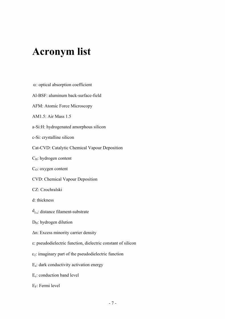
a challenge for achieving the Millennium Developments Goals. In figure 1.1 a map of
the world is deformed as a function of the poverty distribution. The increase of the
African and South Asian territories is clear and in constrast, Europe and North America
almost disappear.
1. Introduction
- 12 -
Figure 1.1: Territory size shows the proportion of the world population in poverty living there (calculated
by multiplying population by one of two poverty indices [http://www.worldmapper.org/]. The human
poverty index uses indicators that capture non-financial elements of poverty, such as life expectancy,
adult literacy, water quality, and children that are underweight. [http://hdr.undp.org]).
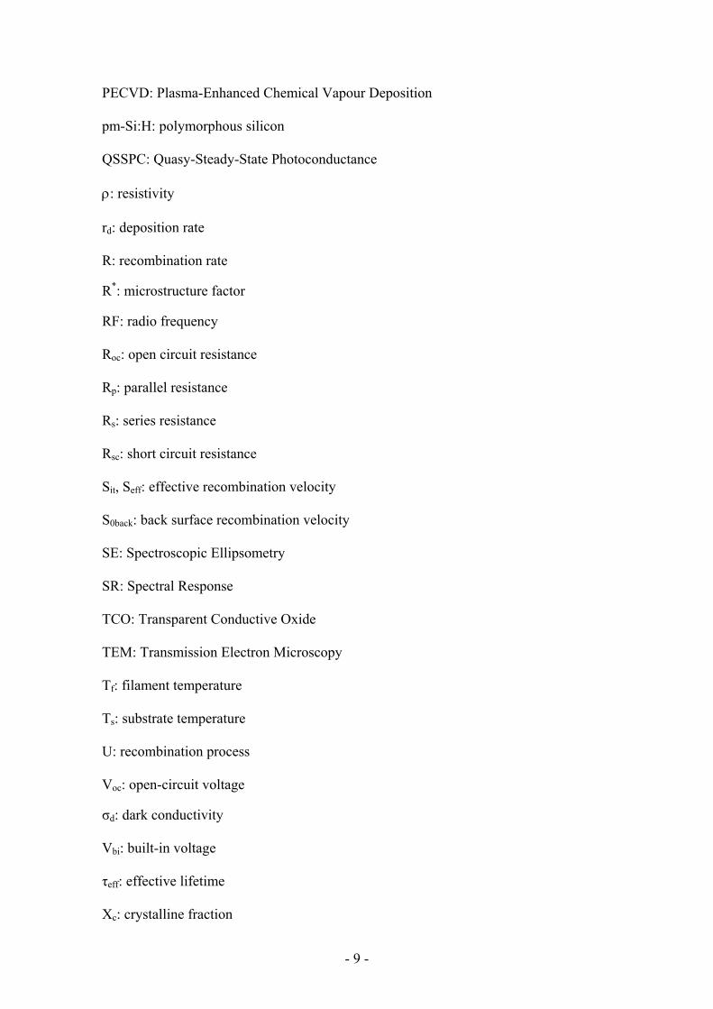
Figure 1.2: Territory size shows the proportion of all people with some electrical power in their homes
living there [http://www.worldmapper.org/]. Electricity access includes that sourced from a publicly used
grid and self-generated electricity. This map shows access, not the quantities of electricity used. The
percentage of people with access to electricity in their own homes is over 97% in Eastern Asia, Eastern
Europe, North America, Western Europe and Japan. 7 of the 10 territories with the lowest access to
electricity are in Africa.
On the contrary, if we look at figure 1.2, we can see the deformed world map, but in this
case, taking into account the electricity supply to the homes in the world. Most of the
electricity-deprived are in sub-Saharan Africa and south Asia. For these people, the day
finishes much earlier than in richer countries due to lack of proper lighting. They
struggle to read by candle light. They lack refrigeration for keeping food and medicines
fresh. Those appliances that they do have are powered by batteries, which eat up a large
share of their incomes. Another hallmark of energy poverty is the use of traditional
biomass in unsustainable, unsafe and inefficient ways. Currently, 2.5 billion people –
40% of the world’s population – rely on traditional biomass such as wood, agricultural

1. Introduction
- 13 -
residues and dung to meet virtually all their cooking energy needs [Birol, 2007]. In
many countries, these resources account for over 90% of all household energy
consumption. These people live mainly in rural areas of Asia and Africa. The use of
biomass is not in itself a cause for concern. But, in practice, it has a number of harmful
consequences for health, the environment and economic and social development.
People, most often women and children, can spend many hours gathering such fuels.
This reduces the time they can devote to more productive activities, such as farming and
education. Wood gathering can also lead to deforestation, resulting in local scarcity of
fuel wood and severe damage to the ecosystem. In addition, reliance on traditional
biomass has a direct impact on human health. The World Health Organization estimates
that each year, 1.3 million people – again, mostly women and children – in developing
countries die as a result of fumes from indoor biomass stoves. Only malnutrition,
HIV/AIDS and lack of clean water and sanitation are greater health threats.
Consequently, meeting basic human needs, such as food and shelter, must be at the
heart of any strategy to alleviate poverty. Energy services help enable those needs to be
met. Indeed, access to energy is a prerequisite to human development. It contributes to
social development by improving health and education and to economic development
by enhancing the productivity of labour and capital.
But the main problem is that the energy system as it is established nowadays, cannot
supply energy for everybody. A non distributed system based on fossils fuel absolutely
politically controlled makes the access to energy to the developing countries difficult
[Scheer, 2002]. So, apart from strong political will and commitment on the part of the
governments to break the vicious circle of energy poverty and human under-
development, investigation and research on new renewable resources (affordable for the
poorest countries and non dependant from energy production countries) has to be done
to allow the development of all the regions in the world.
“The Earth temperature will increase between 1.5ºC and 4ºC in the next 50 years
due to the high presence of greenhouse gases caused by the human activities”
(IPCC, 2007)
1. Introduction
- 14 -
Current trends in energy supply also carry the threat of severe and irreversible
environmental damage – including changes in global climate. If unchecked, energy-
related emissions of carbon dioxide will rise broadly in line with fossil-fuel use through
to 2030, i.e. by more than half. The bulk of the increase will come from developing
countries. The use of low- or zero-carbon renewable energy sources is set to expand
rapidly, but emissions will be driven higher by the inexorable growth in consumption of
fossil energy, especially coal. The latest work by scientists on the potential
consequences of rising concentrations of greenhouse gases in the atmosphere and by
economists on the costs of inaction should leave us in no doubt that the energy path we
are currently on is far from being sustainable [IPCC, 2007].
“Yet there is a solution: to make the transition to renewable sources of energy
and distributed, decentralized energy generation” (Scheer)
Renewable energy sources came from external sources to the Earth, primarily from the
sun. Their basic property is that renewable sources do not run out, in contrast to
conventional energy sources based on fossils fuel as carbon, petrol and gas. Mainly, we
can consider five basic renewable energy sources: wind, biomass, geothermal,
hydrodynamic and solar energy (both, thermal and photovoltaic). All of these forms of
energy are in principle capable of producing large quantities of electricity for present as
well as for future use. The strong points of these forms of energy production are:
- their environmentally friendly nature, as they do not contribute to the production
of carbon dioxide or other greenhouse gasses.
- they allow an energy - distributed scenario, they can supply energetically poor
areas avoiding the energy dependence on other countries.
- these sources for energy production are available in nearly ever-lasting
abundance.
Many studies have been performed considering different scenarios for energy
production and consumption for the next few decades [World Energy Outlook, 2004].
The WEO projections of energy demand and supply are subject to a wide range of
uncertainties including macroeconomic conditions, resource availability, technological
developments and investment flows as well as government energy and environmental
1. Introduction
- 15 -
policies. An increase in the use of renewable sources is always present to satisfy the
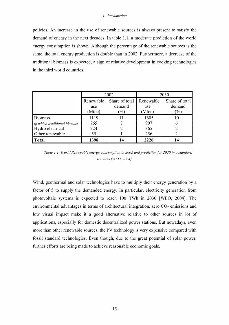
demand of energy in the next decades. In table 1.1, a moderate prediction of the world
energy consumption is shown. Although the percentage of the renewable sources is the
same, the total energy production is double than in 2002. Furthermore, a decrease of the
traditional biomass is expected, a sign of relative development in cooking technologies
in the third world countries.
2002 2030
Renewable use
(Mtoe)
Share of total demand
(%)
Renewableuse
(Mtoe)
Share of total demand
(%) Biomass 1119 11 1605 10 of which traditional biomass 765 7 907 6 Hydro electrical 224 2 365 2 Other renewable 55 1 256 2 Total 1398 14 2226 14
Table 1.1: World Renewable energy consumption in 2002 and prediction for 2030 in a standard
scenario [WEO, 2004].
Wind, geothermal and solar technologies have to multiply their energy generation by a
factor of 5 to supply the demanded energy. In particular, electricity generation from
photovoltaic systems is expected to reach 100 TWh in 2030 [WEO, 2004]. The
environmental advantages in terms of architectural integration, zero CO2 emissions and
low visual impact make it a good alternative relative to other sources in lot of
applications, especially for domestic decentralized power stations. But nowadays, even
more than other renewable sources, the PV technology is very expensive compared with
fossil standard technologies. Even though, due to the great potential of solar power,
further efforts are being made to achieve reasonable economic goals.
1. Introduction
- 16 -
1.2 Photovoltaic energy in the world
The use of photovoltaic systems on a large scale in order to reduce fossil fuel
consumption and greenhouse gas emissions requires that the energy associated with the
construction, operation and decommissioning of PV systems be small compared with
energy production during the system lifetime. That is, the energy payback time should
be short. Over the next few decades at least the energy used to construct PV systems
will be derived primarily from fossil fuels. In the long term "solar breeding" will be
possible, whereby energy for the production of PV systems will be derived from PV
systems. This will reduce or eliminate carbon dioxide emissions associated with PV
system manufacture.
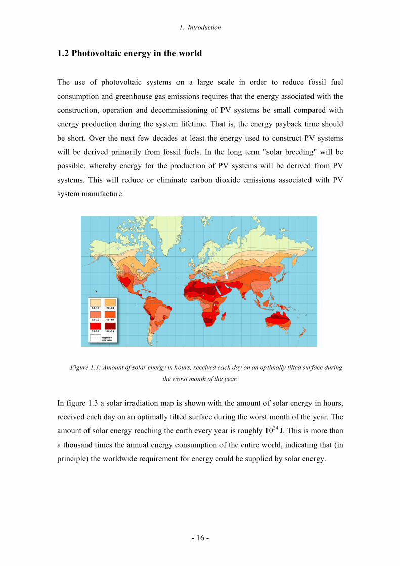
Figure 1.3: Amount of solar energy in hours, received each day on an optimally tilted surface during
the worst month of the year.
In figure 1.3 a solar irradiation map is shown with the amount of solar energy in hours,
received each day on an optimally tilted surface during the worst month of the year. The
amount of solar energy reaching the earth every year is roughly 1024 J. This is more than
a thousand times the annual energy consumption of the entire world, indicating that (in
principle) the worldwide requirement for energy could be supplied by solar energy.
1. Introduction
- 17 -
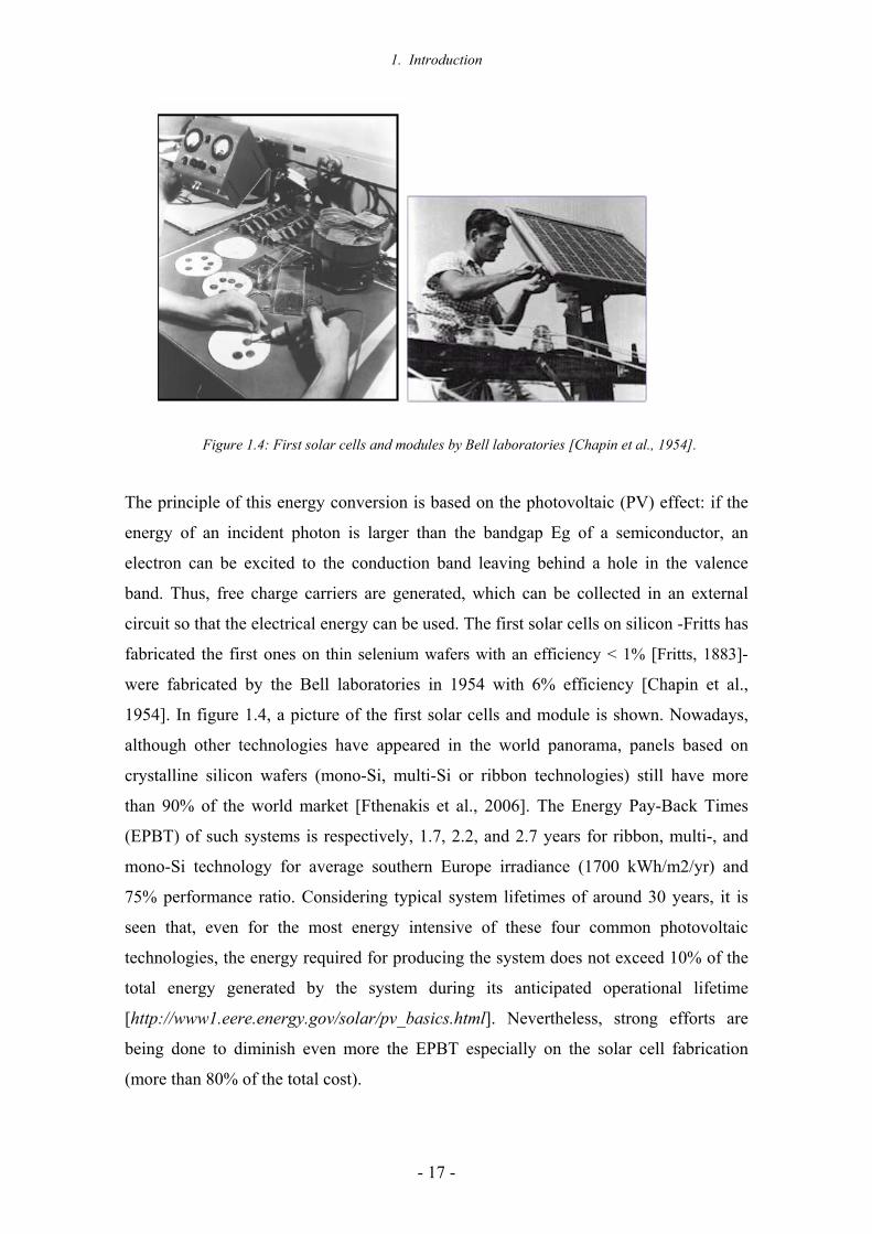
Figure 1.4: First solar cells and modules by Bell laboratories [Chapin et al., 1954].
The principle of this energy conversion is based on the photovoltaic (PV) effect: if the
energy of an incident photon is larger than the bandgap Eg of a semiconductor, an
electron can be excited to the conduction band leaving behind a hole in the valence
band. Thus, free charge carriers are generated, which can be collected in an external
circuit so that the electrical energy can be used. The first solar cells on silicon -Fritts has
fabricated the first ones on thin selenium wafers with an efficiency < 1% [Fritts, 1883]-
were fabricated by the Bell laboratories in 1954 with 6% efficiency [Chapin et al.,
1954]. In figure 1.4, a picture of the first solar cells and module is shown. Nowadays,
although other technologies have appeared in the world panorama, panels based on
crystalline silicon wafers (mono-Si, multi-Si or ribbon technologies) still have more
than 90% of the world market [Fthenakis et al., 2006]. The Energy Pay-Back Times
(EPBT) of such systems is respectively, 1.7, 2.2, and 2.7 years for ribbon, multi-, and
mono-Si technology for average southern Europe irradiance (1700 kWh/m2/yr) and
75% performance ratio. Considering typical system lifetimes of around 30 years, it is
seen that, even for the most energy intensive of these four common photovoltaic
technologies, the energy required for producing the system does not exceed 10% of the
total energy generated by the system during its anticipated operational lifetime
[http://www1.eere.energy.gov/solar/pv_basics.html]. Nevertheless, strong efforts are
being done to diminish even more the EPBT especially on the solar cell fabrication
(more than 80% of the total cost).
1. Introduction
- 18 -
It is important to remark that more than 50% of the solar cell fabrication cost is related
to the production of the raw material, the c-Si wafer [Knapp et al., 2001]. To date, the
PV industry has been strongly dependent on the electronics industry to obtain cheap
substrates using rejected silicon wafers. Two parameters negatively affect this
dependence: the cyclic activity of the electronics industry (varying the price of the
silicon) and the strong increase in the activity of the PV industry saturating the market
[Goetzberger et al., 2002]. Hence, the lack of silicon for PV applications has accelerated
the research on alternative materials and processes to the standard technology of c-Si
solar cells.
1.3 Solar cell technologies
As concluded in the previous section, the interest in cost reduction combined with the
actual lack of crystalline silicon has stimulated research on alternatives to the classical
solar cell fabrication process. In this sense, M. Green has summarized the requirements
for a photovoltaic technology to be successful in the long-term. Based on the argument
that high production volumes will automatically result in total costs approaching the
material costs, these requirements are: (1) thin-film; (2) high-efficiency; (3) non-toxic;
(4) based on abundant materials, and (5) durable [Green, 2006].
Nowadays, the investigation in PV technologies can be grouped in three major areas
[Goetzberger et al., 2003]:
a) Alternative materials
Organics: They have relatively low conversion efficiencies, in the range of 5 percent
for non-commercial solar cells. Their introduction in the market is still a long term
prospect because of the difficulty to obtain stable devices, although the fabrication
process is quite simple [Peumans et al., 2003].
Germanium: It has a structure similar to silicon but a thinner band gap. The obtained
efficiencies do not exceed those of a c-Si solar cell, while the fabrication process is
similar. Nevertheless, germanium-silicon alloys can be stacked in multijunction solar
1. Introduction
- 19 -
cells. Then, each layer responds to different wavelengths of the sunlight because they
have a different band gap. Hence, efficiencies can go beyond the limits of a single
junction solar cell (> 30%) [Green et al., 2006].
Cadmium Telluride/Selenide (CdTe/CdS): These materials are strong light absorbers
with an optimum band-gap of 1.44 eV. Hence, the main advantage is that layers only
need to be about 1µm thick and materials costs can be significantly reduced
[Hamakawa, 2004]. Efficiencies close to 10% have been achieved in commercial
modules by Solar Cells Inc. [Rose et al., 2000]. Moreover, Colorado State Univ. has
recently announced the construction of a plant together with AVA Solar Inc. where
panels will cost less than $1 per watt peak [http://www.avasolar.com/]. Nevertheless, a
concern often expressed about CdS/CdTe solar cells is the effect of cadmium on health
and the environment.
Copper Indium (Gallium) Diselenide (CIS or CIGS): Although they have some
terrestrial applications especially in concentrator systems, they are mainly valuable for
powering space satellites. They are usually fabricated as multi-junction structures, with
a record-setting efficiency of 40.7% achieved by Spectrolab-Boeing using concentration
[Hering, 2007]. The four major challenges for CIS/CISG solar cells are: reducing
manufacturing costs by simplifying and standardizing equipment and processes;
understanding and controlling the electronic properties; developing alternate window
layers (Cd-free); and developing wider band gap materials [Hegedus, 2006].
III-V semiconductors (GaAs, AlGaAs…): They are the most expensive devices,
although they have achieved record efficiencies. They are the most used in aerospace
applications. Their major goal is the possibility to use concentrators to diminish the area
of the device. Using concentrators, record efficiencies of over 42% have been obtained.
b) Thin film a-Si:H and µc-Si:H solar cells
Hydrogenated amorphous silicon p-i-n solar cells are one of the most studied
alternatives because of the abundance of the material. The highest independently
confirmed stabilized efficiency is 12.1%, although commercial modules have stabilized
efficiencies of 6–7% [Hegedus, 2006]. The three major challenges for a-Si:H
1. Introduction
- 20 -
technology are: to increase the stabilized module efficiency to 10–12%; to minimize or
eliminate the self-limiting degradation; and to increase the film deposition rate without
sacrificing performance.
Furthermore, the multi-junction technology can be also applied combining a-Si:H with
µc-Si:H solar cells. Promising results with stable efficiencies up to 13% have been
obtained in triple stack a-Si:H/µc-Si:H/µc-Si:H solar cells. These devices are less
sensitive to photodegradation, and can reach module efficiencies of up to 12%
[Yamamoto et al., 2005].
c) Alternative c-Si solar cells
In spite of the economic problems previously mentioned, crystalline silicon as a base
material in the PV industry for terrestrial applications continues to be a good alternative.
The good properties of c-Si in terms of low degradation, low environmental impact,
abundance as raw material and feasibility to reach high efficiencies are remarkable. The
24.7% world record efficiency on c-Si has been published by the group of M. Green
with the so-called PERL structure (figure 1.5) [Zhao et al., 1999]. Although this result
reflects a great technological development, it is a long, complicated and expensive
fabrication process. Consequently, there are different lines of investigation aiming to
reach similar efficiencies but with drastically reduced costs.
Figure 1.5: PERL (passivated emitter, rear locally-diffused) solar cell structure fabricated by the group
of M. Green at University of New South Wales [Zhao et al., 1999].
One solution is to use low quality silicon prepared especially for the photovoltaic
industry: solar-grade silicon. This is already being carried out in the industry with
1. Introduction
- 21 -
multicrystalline silicon. Approximately 30% of the present production of modules is
based on multicrystalline silicon. This alternative is cheaper than monocrystalline
silicon, but the module efficiency (15.3% record [King et al., 1994]) is still far from that
obtained with c-Si (22.7% record [Zhao et al., 1997] and 19.7% on very large area
[Rose et al., 2006]). On the other hand, other investigation lines focus their efforts on
reducing not the quality but the quantity of silicon by using thinner wafers (figure 1.6).
The main problem of thin wafers is their tendency to warp at the high temperatures (~
1000ºC) involved in the standard fabrication process. Low cost multicrystalline silicon
wafers are not compatible with high temperature steps either, but in this case due to
strong lifetime degradation [Schultz, 2004].
Figure 1.6: Very thin solar cell (20.2% on 37µm) fabricated at ISE. They have also the record 21.2% on
a 75µm wafer without wafer warpage [Glunz et al., 2005].
Therefore, low temperature surface passivation schemes using thin films of
hydrogenated amorphous silicon (a-Si:H) [Kunst et al., 2002], [Voz et al., 2003], silicon
carbide (a-SiCx:H) [Martin et al., 2001] or silicon nitride (a-SiNx:H) [Lauinger et al.,
1996], [Leguijt et al., 1996] have gained special interest due to their compatibility with
both thin and low quality c-Si substrates. The heteroestructure formed between a-Si:H
and c-Si is particularly interesting, since intrinsic films can be used for passivation and
doped ones to form either the heterojunction emitter or the back contact. In this sense,
double-side heterojunction devices can be fabricated in a fully low temperature process.
1. Introduction
- 22 -
1.4 Development of silicon heterojunction solar cells
The investigation of heterojunction silicon solar cells started in 1974 when Fuhs et al.
first proposed to use heterojunctions of amorphous silicon emitter on a crystalline
substrate for solar cells [Fuhs et al., 1974]. Then, in 1985 the first heterojunction solar
cell was fabricated [Hamakawa et al., 1985]. From this moment, many research groups
worldwide were interested in the technological development of a-Si:H/c-Si
heterojunctions as an alternative to traditional diffused emitters. The heterojunction is
formed by depositing a thin a-Si:H layer on the c-Si wafer at temperatures typically
below 200ºC. In addition, it is a simple process with a relatively low manufacturing
cost. The potential of this technology was definitely demonstrated by Sanyo in 1991
with the structure denominated HIT (Heterojunction with Intrinsic Thin layer) [Iwamoto
et al., 1991] that has been continuously developed resulting in an outstanding 22%
efficiency in 100 cm2 solar cells [Taguchi et al., 2005], [http://us.sanyo.com].
Moreover, Sanyo has also achieved 19.5% efficiencies in mass produced modules
[Tanaka et al., 2003]. The main difference compared to the first heterostructures is the
inclusion of a thin intrinsic amorphous silicon layer between the doped layer and the
wafer to improve the properties at the interface. Besides, Sanyo has applied the HIT
concept also to low temperature BSF contacts, as in the bifacial device shown in figure
1.7. These solar cells are fabricated on CZ n-type wafers of thickness 250 µm. The
deposition technique used for all the a-Si:H layers is Plasma Enhanced Chemical
Vapour Deposition (PECVD). The device is finished with the deposition of a TCO
antireflective coating followed by the metallic electrodes. Most details about the
fabrication process have not been revealed by the company.
Figure 1.7: Structure of the bifacial heterojunction solar cells fabricated by Sanyo.
1. Introduction
- 23 -
The main advantages of heterojunction devices are summarized next:
- Potential for high efficiency solar cells: as demonstrated by Sanyo with
excellent results and competitive technology in the present market.
- Good passivation properties: given by the amorphous silicon used either as
heterojunction emitter or low temperature BSF. The deposition conditions of the
material can be optimized in order to obtain the desired properties in the final
device.
- Excellent stability: the base material of the structure continues to be crystalline
silicon. In this way, the typical degradation (Staebler-Wronski effect) observed
in amorphous silicon solar cells does not take place. Actually, the extremely thin
a:Si-H layers do not contribute to power generation and have only an interface
passivation purpose.
- Low temperatures throughout the process (< 200ºC) that will allow
technological development with thin or low quality crystalline silicon wafers.
- Simplicity of the process: The fabrication process is conceptually the same for
the emitter and the BSF contact, not only regarding a-Si:H deposition but also
the TCO and metallic contacts on both sides. Thus, the fabrication time is less
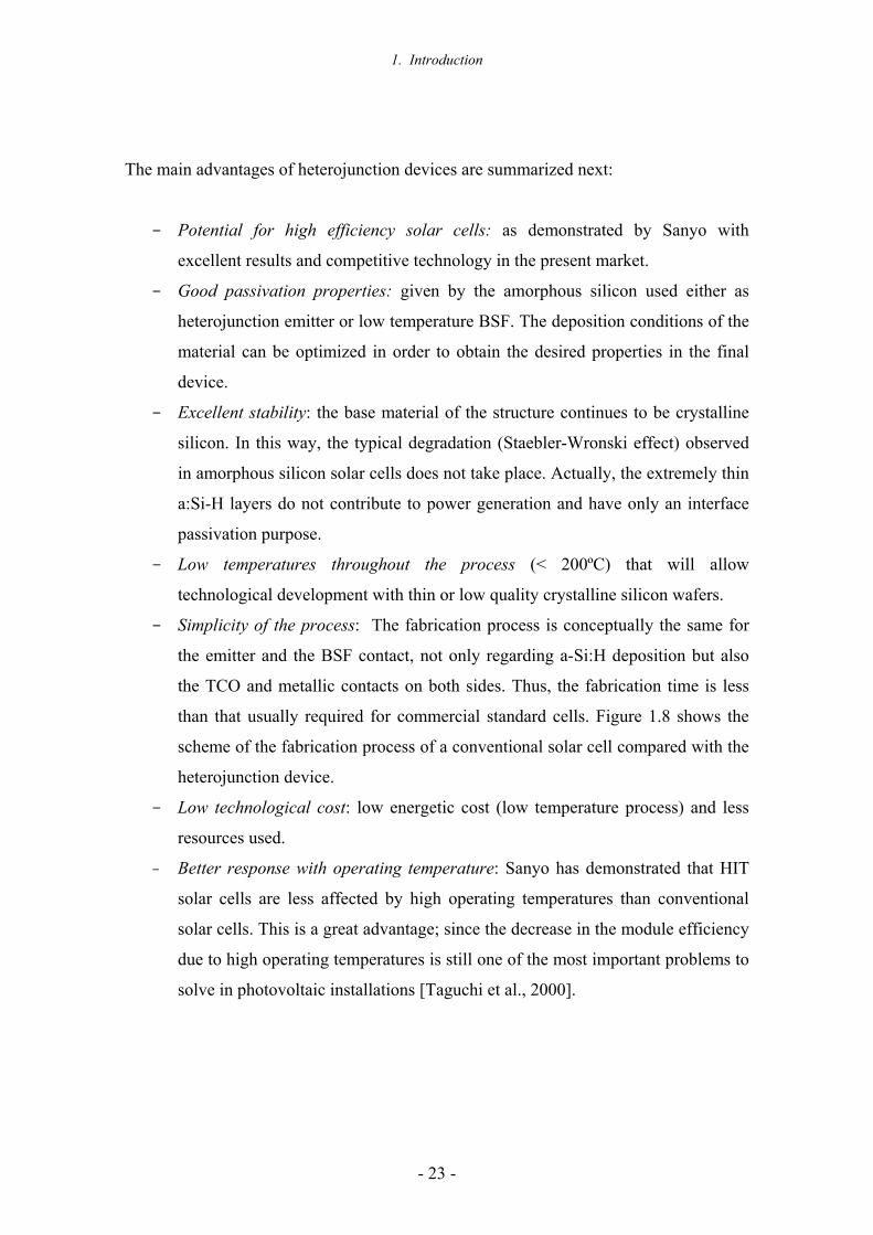
than that usually required for commercial standard cells. Figure 1.8 shows the
scheme of the fabrication process of a conventional solar cell compared with the
heterojunction device.
- Low technological cost: low energetic cost (low temperature process) and less
resources used.
- Better response with operating temperature: Sanyo has demonstrated that HIT
solar cells are less affected by high operating temperatures than conventional
solar cells. This is a great advantage; since the decrease in the module efficiency
due to high operating temperatures is still one of the most important problems to
solve in photovoltaic installations [Taguchi et al., 2000].
1. Introduction
- 24 -
Figure 1.8: Scheme of the fabrication steps for a conventional solar cell compared to a heterojunction
device. The temperatures involved in the different fabrication steps are indicated [Roca et al., 2004].
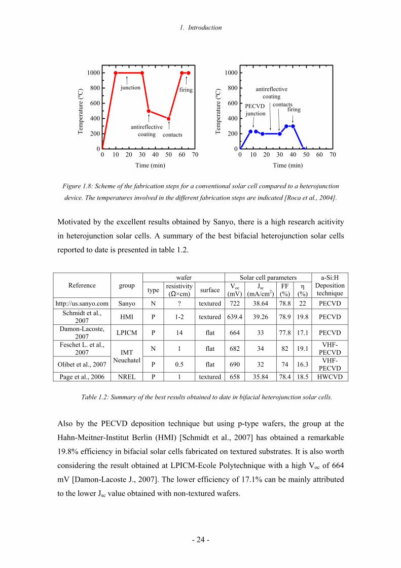
Motivated by the excellent results obtained by Sanyo, there is a high research acitivity
in heterojunction solar cells. A summary of the best bifacial heterojunction solar cells
reported to date is presented in table 1.2.
wafer Solar cell parameters Reference group
type resistivity (Ω×cm) surface Voc
(mV)Jsc
(mA/cm2)FF (%)
η (%)
a-Si:H Deposition technique
http://us.sanyo.com Sanyo N ? textured 722 38.64 78.8 22 PECVD Schmidt et al.,
2007 HMI P 1-2 textured 639.4 39.26 78.9 19.8 PECVD
Damon-Lacoste, 2007 LPICM P 14 flat 664 33 77.8 17.1 PECVD
Feschet L. et al., 2007 N 1 flat 682 34 82 19.1 VHF-
PECVD
Olibet et al., 2007
IMT Neuchatel P 0.5 flat 690 32 74 16.3 VHF-
PECVD Page et al., 2006 NREL P 1 textured 658 35.84 78.4 18.5 HWCVD
Table 1.2: Summary of the best results obtained to date in bifacial heterojunction solar cells.
Also by the PECVD deposition technique but using p-type wafers, the group at the
Hahn-Meitner-Institut Berlin (HMI) [Schmidt et al., 2007] has obtained a remarkable
19.8% efficiency in bifacial solar cells fabricated on textured substrates. It is also worth
considering the result obtained at LPICM-Ecole Polytechnique with a high Voc of 664
mV [Damon-Lacoste J., 2007]. The lower efficiency of 17.1% can be mainly attributed
to the lower Jsc value obtained with non-textured wafers.
0 10 20 30 40 50 60 700
200
400
600
800
1000
firingcontacts
antireflectivecoating
PECVD junction
Tem
pera
ture
(ºC
)
Time (min)
0 10 20 30 40 50 60 700
200
400
600
800
1000
firing
contactsantireflective
coating
junction
Tem
pera
ture
(ºC
)
Time (min)
1. Introduction
- 25 -
Excellent results have been also presented by the Institute of Microtechnique (IMT) at
Université de Neuchatel. This group has great experience in amorphous silicon thin film
solar cells fabricated by the Very High Frequency PECVD technique. This deposition
method allows higher deposition rates and is less aggressive than the conventional
PECVD technique. Thus, less interface damage is expected, which is very desirable for
heterojunction devices. They have worked with both n- and p-type wafers, obtaining
excellent Voc values only surpassed by Sanyo [Feschet L. et al., 2007] and efficiencies
over 19% on n-type wafers. To date, the IMT group has limited this research to flat
wafers.
Finally, the group at the National Renewable Energy Laboratory (NREL) has also
obtained very good results with a completely different deposition technique, the Hot-
Wire CVD. In this technique, the absence of plasma has some advantages with respect
to the other deposition methods as explained in the next section. The NREL group has
demonstrated the possibility to obtain good quality layers and high efficiency
heterojunction solar cells by HWCVD [Branz et al., 2007]. The best efficiency obtained
until now is 18.5% on p-type textured substrates with a remarkable Voc of 658 mV
[Page et al., 2006].
1.5 Why the HWCVD technique for heterojunction solar cells?
Although the most common a-Si:H /µc-Si:H deposition technique is Plasma-Enhanced
CVD, the Hot-Wire CVD technique has appeared as an interesting alternative in the last
two decades. This technique was first used to deposit a-Si:H by Wiesmann in 1979
[Wiesmann et al., 1979] and later on by Matsumura who deposited the first
microcrystalline layers [Matsumura, 1991]. Matsumura also introduced the term
Catalytic CVD (Cat-CVD) to describe the catalytic nature of the reactions taking place
at the wire surface. Nowadays, the two different terms coexist in the literature to
describe the same deposition process. Hot-Wire CVD is now becoming a mature
technique in the field of thin silicon film deposition.
1. Introduction
- 26 -
It offers several features that overcome some limitations in the PECVD technique:
a) absence of ion bombardment and dust formation during deposition [Schropp,
2004]
b) high deposition rates, especially for µc-Si:H films [Nelson et al., 2001]
c) low equipment implementation and upkeep costs
d) high gas utilization (tens of %) [Honda et al., 2000]
e) easy scalability to large areas [Ishibashi, 2001]
Presently, the Hot-Wire CVD technique can be used to obtain devices with state-of-the-
art properties: thin film solar cells [Schropp et al., 2007], thin-film-transistors (TFT)
[Stannowski et al., 2003], microelectronic mechanical systems (MEMS) and, also,
heterojunction solar cells [Branz et al., 2007]. Moreover, thanks to the simplicity of its
geometry, large area HWCVD set-ups have been developed allowing homogeneous
deposition over surfaces as large as 92 x 73 cm [Matsumura et al., 2003]. Since 2000,
the HWCVD community meets in a biannual conference where the best results and
advances are presented and discussed.
For all these reasons, and especially due to the possibility of sharing the HWCVD set-
up and knowledge in thin silicon films of the Solar Energy Group at the Universitat de
Barcelona, in this work we have investigated a-Si:H/c-Si heterojunction solar cells
fabricated by HWCVD.
2. Device fabrication process
- 27 -
Chapter 2: Device fabrication
process
“A goal without a plan is just a wish”
Antoine de Saint-Exupery
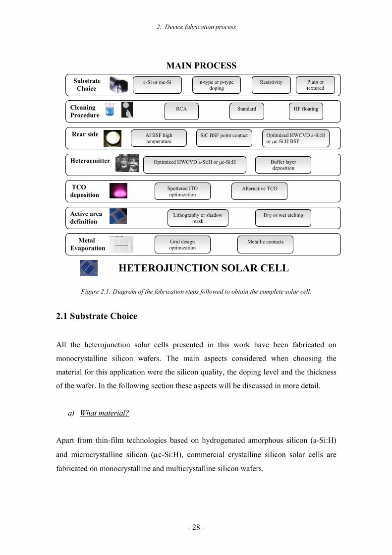
In this chapter, we briefly describe the process followed in this thesis to fabricate
heterojunction silicon solar cells. In figure 2.1, a diagram of the fabrication process
shows the sequential tasks to be done. Some of the lasts steps, especially the emitter and
the rear side contact deposition, can be partially modified depending on the specific
device structure. Most of the work is done in the Clean Room located at the DEE in the
UPC, but the a-Si:H films are deposited by HWCVD at the Departament de Física
Aplicada i Òptica in the Universitat de Barcelona.
2. Device fabrication process
- 28 -
Figure 2.1: Diagram of the fabrication steps followed to obtain the complete solar cell.
2.1 Substrate Choice
All the heterojunction solar cells presented in this work have been fabricated on
monocrystalline silicon wafers. The main aspects considered when choosing the
material for this application were the silicon quality, the doping level and the thickness
of the wafer. In the following section these aspects will be discussed in more detail.
a) What material?
Apart from thin-film technologies based on hydrogenated amorphous silicon (a-Si:H)
and microcrystalline silicon (µc-Si:H), commercial crystalline silicon solar cells are
fabricated on monocrystalline and multicrystalline silicon wafers.
Substrate Choice
Cleaning Procedure
Rear side
TCO deposition
Active area definition
Metal Evaporation
Heteroemitter
c-Si or mc-Si n-type or p-type doping
Resistivity Plain or textured
RCA Standard HF floating
Al BSF high temperature
SiC BSF point contact Optimized HWCVD a-Si:H or µc-Si:H BSF
Optimized HWCVD a-Si:H or µc-Si:H Buffer layer deposition
Sputtered ITO optimization
Alternative TCO
Lithography or shadow mask
Dry or wet etching
Grid design optimization
Metallic contacts
MAIN PROCESS
HETEROJUNCTION SOLAR CELL
2. Device fabrication process
- 29 -
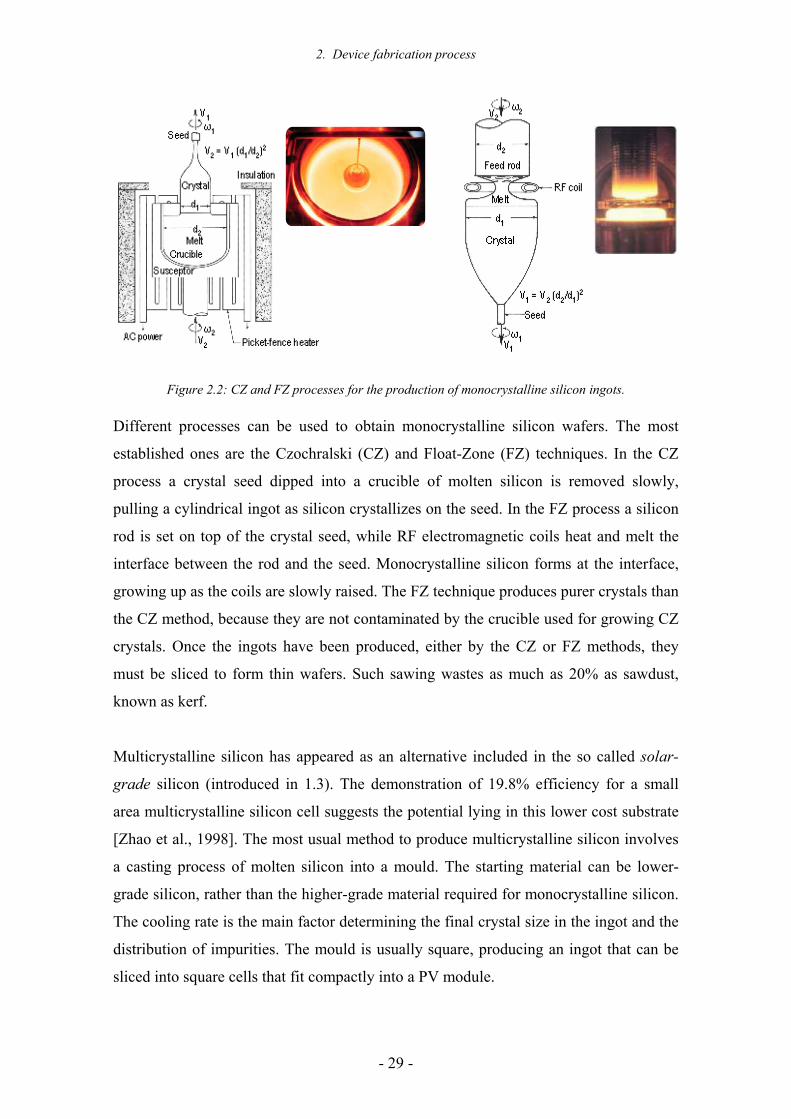
Figure 2.2: CZ and FZ processes for the production of monocrystalline silicon ingots.
Different processes can be used to obtain monocrystalline silicon wafers. The most
established ones are the Czochralski (CZ) and Float-Zone (FZ) techniques. In the CZ
process a crystal seed dipped into a crucible of molten silicon is removed slowly,
pulling a cylindrical ingot as silicon crystallizes on the seed. In the FZ process a silicon
rod is set on top of the crystal seed, while RF electromagnetic coils heat and melt the
interface between the rod and the seed. Monocrystalline silicon forms at the interface,
growing up as the coils are slowly raised. The FZ technique produces purer crystals than
the CZ method, because they are not contaminated by the crucible used for growing CZ
crystals. Once the ingots have been produced, either by the CZ or FZ methods, they
must be sliced to form thin wafers. Such sawing wastes as much as 20% as sawdust,
known as kerf.
Multicrystalline silicon has appeared as an alternative included in the so called solar-
grade silicon (introduced in 1.3). The demonstration of 19.8% efficiency for a small
area multicrystalline silicon cell suggests the potential lying in this lower cost substrate
[Zhao et al., 1998]. The most usual method to produce multicrystalline silicon involves
a casting process of molten silicon into a mould. The starting material can be lower-
grade silicon, rather than the higher-grade material required for monocrystalline silicon.
The cooling rate is the main factor determining the final crystal size in the ingot and the
distribution of impurities. The mould is usually square, producing an ingot that can be
sliced into square cells that fit compactly into a PV module.
2. Device fabrication process
- 30 -
Another group of processes to obtain crystalline silicon are known by the general name
of ribbon growth. These methods can directly produce multicrystalline silicon wafers,
thus avoiding the slicing step required for cylindrical ingots. The most developed ribbon
growth technique is the Edge-defined Film-fed Growth (EFG) [Wald et al., 1981],
which is already in high volume commercial production [Schmidt et al., 2002].
In this thesis, we have centralised our efforts in optimizing solar cells on
monocrystalline silicon because of the novelty of the investigation in heterojunction
devices fabricated by HWCVD. Both CZ and FZ c-Si wafers have been used depending
on the specific experiment in course. Detailed passivation studies and optimization of
heterojunctions were preferably performed on FZ substrates (ρ = 1-10 Ωcm) in order to
assure very low bulk recombination. Thereby, the measured effective lifetime is mainly
determined by the interface between a-Si:H and c-Si [Martin, 2004]. Complete solar
cells were manufactured on both FZ and CZ substrates.
b) Which doping?
Traditionally, industrial solar cells have been fabricated onto p-type wafers for a few
reasons [Goetzberger et al., 2003]. The most important one was the simplicity to obtain
this material as surplus from the electronic industry (section 1.2). Recently, the
possibility of using n-type wafers has appeared as a feasible alternative due to the
shortage of crystalline silicon.
In the case of heterojunction solar cells, the record efficiency reported by Sanyo was
actually obtained using n-type wafers [Taguchi et al., 2005]. In agreement, Wang et al.
have proposed a series of advantages when using n-type wafers in heterojunction solar
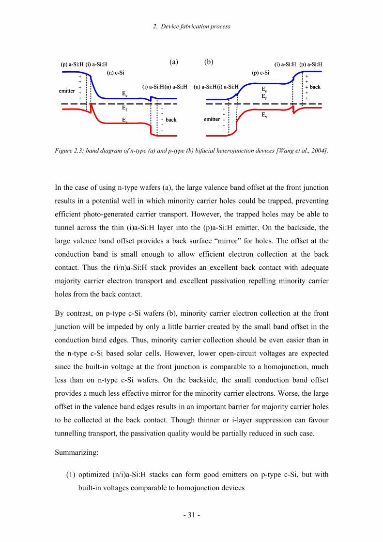
cells [Wang et al., 2004]. Figure 2.3 shows the band diagram of bifacial heterojunction
devices based on both n-type (a) and p-type (b) c-Si substrates. It is important to remark
the accepted larger a-Si:H/c-Si band offset in the valence band (Ev) than in the
conduction band (Ec) [Stangl et al., 2001]. This effect reflects, for instance, the small
difference between the electron affinities of a-Si:H (3.9 eV) and c-Si (4.05 eV).
2. Device fabrication process
- 31 -
(p) a-Si:H (i) a-Si:H
(i) a-Si:H(n) a-Si:H
(p) c-Si
Ec
Ef
Ev
emitter
back
+++++
-----
back(i) a-Si:H(n) a-Si:H
(i) a-Si:H (p) a-Si:H
EcEf
Evemitter
+++++
-----
(n) c-Si (p) a-Si:H (i) a-Si:H
(i) a-Si:H(n) a-Si:H
(p) c-Si
Ec
Ef
Ev
emitter
back
+++++
-----
back(i) a-Si:H(n) a-Si:H
(i) a-Si:H (p) a-Si:H
EcEf
Evemitter
+++++
-----
(n) c-Si
Figure 2.3: band diagram of n-type (a) and p-type (b) bifacial heterojunction devices [Wang et al., 2004].
In the case of using n-type wafers (a), the large valence band offset at the front junction
results in a potential well in which minority carrier holes could be trapped, preventing
efficient photo-generated carrier transport. However, the trapped holes may be able to
tunnel across the thin (i)a-Si:H layer into the (p)a-Si:H emitter. On the backside, the
large valence band offset provides a back surface “mirror” for holes. The offset at the
conduction band is small enough to allow efficient electron collection at the back
contact. Thus the (i/n)a-Si:H stack provides an excellent back contact with adequate
majority carrier electron transport and excellent passivation repelling minority carrier
holes from the back contact.
By contrast, on p-type c-Si wafers (b), minority carrier electron collection at the front
junction will be impeded by only a little barrier created by the small band offset in the
conduction band edges. Thus, minority carrier collection should be even easier than in
the n-type c-Si based solar cells. However, lower open-circuit voltages are expected
since the built-in voltage at the front junction is comparable to a homojunction, much
less than on n-type c-Si wafers. On the backside, the small conduction band offset
provides a much less effective mirror for the minority carrier electrons. Worse, the large
offset in the valence band edges results in an important barrier for majority carrier holes
to be collected at the back contact. Though thinner or i-layer suppression can favour
tunnelling transport, the passivation quality would be partially reduced in such case.
Summarizing:
(1) optimized (n/i)a-Si:H stacks can form good emitters on p-type c-Si, but with
built-in voltages comparable to homojunction devices
(a) (b)
2. Device fabrication process
- 32 -
(2) optimized (p/i)a-Si:H stacks can form great emitters on n-type c-Si, with built-in
voltages significantly higher than in homojunction devices
(3) optimized (i/p)a-Si:H stacks can form fair back contacts on p-type c-Si based
solar cells
(4) optimized (i/n)a-Si:H stacks can form excellent back contacts on n-type c-Si
based solar cells
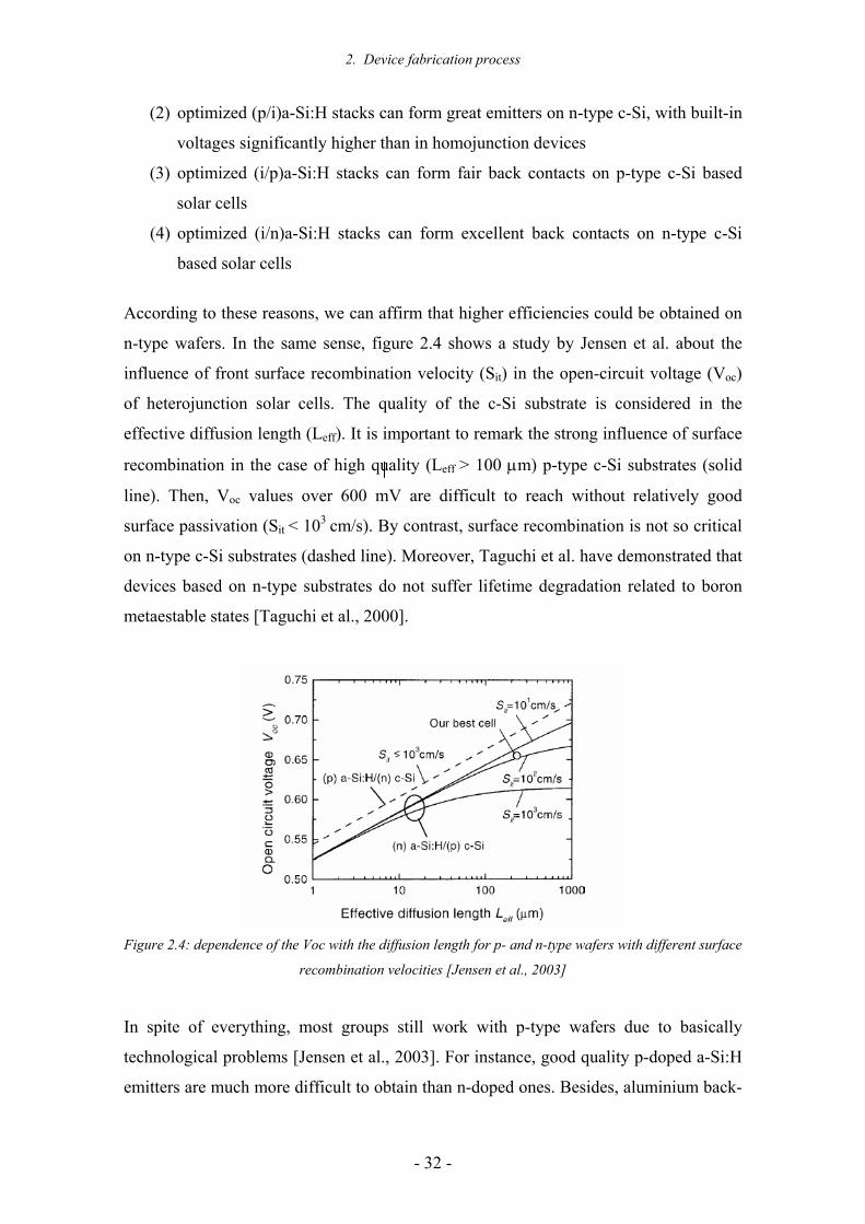
According to these reasons, we can affirm that higher efficiencies could be obtained on
n-type wafers. In the same sense, figure 2.4 shows a study by Jensen et al. about the
influence of front surface recombination velocity (Sit) in the open-circuit voltage (Voc)
of heterojunction solar cells. The quality of the c-Si substrate is considered in the
effective diffusion length (Leff). It is important to remark the strong influence of surface
recombination in the case of high quality (Leff > 100 µm) p-type c-Si substrates (solid
line). Then, Voc values over 600 mV are difficult to reach without relatively good
surface passivation (Sit < 103 cm/s). By contrast, surface recombination is not so critical
on n-type c-Si substrates (dashed line). Moreover, Taguchi et al. have demonstrated that
devices based on n-type substrates do not suffer lifetime degradation related to boron
metaestable states [Taguchi et al., 2000].
Figure 2.4: dependence of the Voc with the diffusion length for p- and n-type wafers with different surface
recombination velocities [Jensen et al., 2003]
In spite of everything, most groups still work with p-type wafers due to basically
technological problems [Jensen et al., 2003]. For instance, good quality p-doped a-Si:H
emitters are much more difficult to obtain than n-doped ones. Besides, aluminium back-
2. Device fabrication process
- 33 -
surface-field (Al-BSF) contacts can not be used in the case of n-type c-Si wafers. Due to
these technological reasons the scientific community has not totally solved the debate
about the best doping type for heterojunction silicon solar cells.
c) What thickness?
Traditionally, wafers over 300 microns thick have been used to fabricate crystalline
silicon solar cells. This thickness gives the required mechanical strength for handling
and the resistance to the stress due to different contraction of layers on front and rear
surfaces during fabrication. However, just the substrates represent currently close to
40% of the final module cost, which has to be reduced to be competitive with other
energy sources [Quang et al., 2004]. For example, the use of 150 µm thick wafers would
increase the production around 30% with a simultaneous cost reduction of 14% [Quang
et al., 2004]. Swanson announces wafer thicknesses close to 120 µm for c-Si and 180
µm for mc-Si in industrial production by 2012 [Swanson et al., 2004]. A clear example
of the present effort to save c-Si is a recently developed structure denominated SLIVER
[Stocks et al., 2003] that proposes the cross section of 1 mm thick c-Si wafers in strips
of thickness inferior to 100 µm. This new structure achieves 17.5% efficiency with a
saving of material superior to a factor 12 with respect to conventional technologies.
Concerning the standard process of silicon growth and wafer sawing, it is already
relatively simple to obtain wafers around 200 µm with much reduced kerf losses. In
addition, new sawing techniques have been developed in the last decade (multi-wire
sawing), that allow wafer thicknesses below 100 µm [Funke et al., 2004]. In order to
maintain a high cell performance as the substrate thickness is reduced, much attention
must be paid to the passivation at both surfaces of the cell (reduce interface defect
density). Back surface recombination can remarkably affect the final device efficiency
when the wafer thickness becomes comparable to the carrier diffusion length [Aberle,
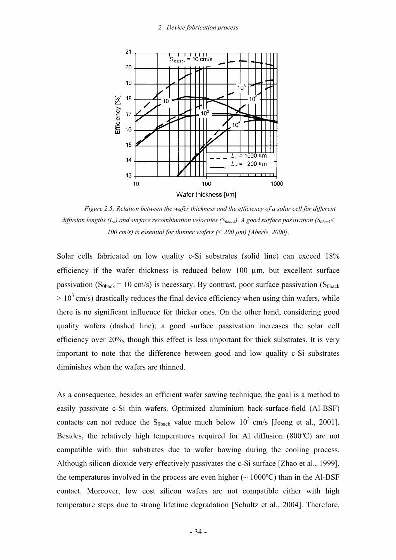
2000]. Figure 2.5 shows the solar cell efficiency as a function of the wafer thickness for
different back surface recombination velocities (S0back). Two main situations have been
considered: a long diffusion length (Ln = 1000 µm) corresponding to good quality c-Si
wafers and a short one (Ln = 200 µm) for lower quality substrates.
2. Device fabrication process
- 34 -
Figure 2.5: Relation between the wafer thickness and the efficiency of a solar cell for different
diffusion lengths (Ln) and surface recombination velocities (S0back). A good surface passivation (S0back<
100 cm/s) is essential for thinner wafers (< 200 µm) [Aberle, 2000].
Solar cells fabricated on low quality c-Si substrates (solid line) can exceed 18%
efficiency if the wafer thickness is reduced below 100 µm, but excellent surface
passivation (S0back = 10 cm/s) is necessary. By contrast, poor surface passivation (S0back
> 103 cm/s) drastically reduces the final device efficiency when using thin wafers, while
there is no significant influence for thicker ones. On the other hand, considering good
quality wafers (dashed line); a good surface passivation increases the solar cell
efficiency over 20%, though this effect is less important for thick substrates. It is very
important to note that the difference between good and low quality c-Si substrates
diminishes when the wafers are thinned.
As a consequence, besides an efficient wafer sawing technique, the goal is a method to
easily passivate c-Si thin wafers. Optimized aluminium back-surface-field (Al-BSF)
contacts can not reduce the S0back value much below 103 cm/s [Jeong et al., 2001].
Besides, the relatively high temperatures required for Al diffusion (800ºC) are not
compatible with thin substrates due to wafer bowing during the cooling process.
Although silicon dioxide very effectively passivates the c-Si surface [Zhao et al., 1999],
the temperatures involved in the process are even higher (~ 1000ºC) than in the Al-BSF
contact. Moreover, low cost silicon wafers are not compatible either with high
temperature steps due to strong lifetime degradation [Schultz et al., 2004]. Therefore,
2. Device fabrication process
- 35 -
low temperature surface passivation schemes based on thin films of hydrogenated
amorphous silicon (a-Si:H) [Kunst et al., 2002], [Voz et al., 2003], silicon nitride (a-
SiNx:H) [Lauinger et al., 1996], [Leguijt et al., 1996] and silicon carbide (a-SiCx:H)
[Martin et al., 2001] have gained special interest due to their compatibility with both
thin and low quality c-Si substrates. A detailed discussion on these approaches can be
found in section 2.3.
2.2 Cleaning procedures
Before depositing any layer on the c-Si surface, it must be cleaned from organic and
inorganic impurities in order to obtain high performance devices. The cleaning
procedure is also essential to prevent contamination of the process equipment and
assure reliable results.
1012 1013 1014 1015 1016 1017
1x10⁻⁵
1x10⁻⁴
Effe
ctiv
e lif
etim
e, τ
eff (s
)
Minority carrier density, ∆n
native oxide removed native oxide left
Figure 2.6 Effective lifetime vs minority carrier density curves measured by QSSPC for the same
emitter deposited either on the native oxide () or in a sample where it has been totally removed ().
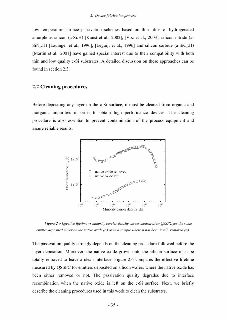
The passivation quality strongly depends on the cleaning procedure followed before the
layer deposition. Moreover, the native oxide grown onto the silicon surface must be
totally removed to leave a clean interface. Figure 2.6 compares the effective lifetime
measured by QSSPC for emitters deposited on silicon wafers where the native oxide has
been either removed or not. The passivation quality degrades due to interface
recombination when the native oxide is left on the c-Si surface. Next, we briefly
describe the cleaning procedures used in this work to clean the substrates.

2. Device fabrication process
- 36 -
a) RCA cleaning
The RCA cleaning is the industrial standard process for removing contaminants from
the c-Si surface. Werner Kern developed the basic procedure in 1965 while he was
working for Radio Corporation of America, hence the RCA name. The RCA cleaning
procedure consists of three main sequential steps:
I. Organic Cleaning: Removal of insoluble organic contaminants with a
H2O:H2O2:NH4OH (5:1:1) solution.
II. Oxide Strip: Removal of thin silicon dioxide layer as a result of (I) where
metallic contaminants may accumulate, using a diluted H2O:HF (50:1)
solution.
III. Ionic Cleaning: Removal of ionic and heavy metallic contaminants using a
H2O:H2O2: HCl (6:1:1) solution.
The RCA cleaning does not etch silicon, only a very thin silicon dioxide layer is
removed during step II. The procedure was also designed to prevent reincorporation of
metallic contaminants from solution back to the c-Si surface. When the RCA cleaning is
finished, the polished side of the wafer should look specular with no residue.
b) Standard cleaning
A simpler procedure to prepare the c-Si surface is generally known as standard cleaning.
The standard cleaning procedure consists of two main steps:
I. Organic coating removal: The wafers are immersed into a H2SO4:H2O2 (2:1)
solution, generally called piranha. Organic residues are removed while metallic
contaminants form soluble complexes. The mixture is self-heating and solution
looses its effectiveness when it cools down after about 10 minutes.
II. Oxide removal: The thin silicon dioxide layer grown during I is removed by
dipping the wafer in a H2O:HF (50:1) solution until the surface becomes
hydrophobic.
2. Device fabrication process
- 37 -
The standard cleaning is usually adequate for wafers that have been accurately handled
before being processed. When that is not the case, at least one complete RCA cleaning
is required to assure good and reproducible results.
2.3 Rear side fabrication
The rear side of the solar cell should accomplish three main conditions:
Good surface passivation to reduce recombination losses
Good internal reflection to profit irradiance at longer wavelengths
Good electrical contact to reduce the series resistance of the device
2.3.1 High temperature BSF
The simplest solution used in the photovoltaic industry for the rear side is an
Aluminium Back-Surface-Field contact (Al-BSF). The standard process consists in the
deposition of an aluminium screen-printing paste (~ 20 µm) by serigraphy and a post
annealing reaching temperatures up to 800ºC [Veschetti, 2005]. The final structure is a
three layer system: a heavily Al-doped (1%) silicon layer, an AlSi compact alloy and a
phase-mixed AlSi/Al2O3 layer [Huster, 2005]. The main problem of Al-BSF contacts is
wafer bowing during the cooling process, which is especially important in thinner
substrates (< 200 µm). Although some solutions to reduce this wafer bowing have
partially succeeded [Huster, 2005], the elimination of high temperature steps is
definitely attractive. On the other hand, back surface recombination velocity with
optimized Al-BSF contacts can not be reduced much below 103 cm/s [Jeong et al.,
2001], whereas internal reflection is usually below 70% [Hermle et al., 2005].
2.3.2 Low temperature passivation
Here, we consider low temperature back surface passivation alternatives to Al-BSF
contacts. These structures are based on dielectric films which can provide much lower
surface recombination velocities (Sback < 102 cm/s), but require a point contact patterning
of the backside as proposed with the PERC (Passivated Emitter and Rear Cell) concept
2. Device fabrication process
- 38 -
[Green et al., 1990]. The internal reflection of these structures generally exceeds 90%,
which is important to profit long wavelength irradiance in thin substrates [Hermle et al.,
2005]. Although point contact formation based on photolithography is unlikely to
succeed in industrial production, the recently developed laser fired contact (LFC)
technology has really great potential for future applications [Schneidorlöchner et al.,
2002]. However, the laser set-up and the beam positioning system introduce a relatively
complex additional process.
a) Silicon Nitride
Hydrogenated amorphous silicon nitride (a-SiNx:H) deposited by Plasma-Enhanced
Chemical Vapour Deposition (PECVD) is one of the most developed low temperature
(< 500ºC) passivation alternatives. Effective surface recombination velocity values of
just 4 and 20 cm/s have been reported on p-type (1 Ωcm) [Lauinger et al., 1995]
[Mäckel et al., 2002] [Schmidt et al., 2001] and n-type c-Si (18 Ωcm) [Kunst et al.,
2002b], respectively. The excellent passivating properties of a-SiNx:H films have been
attributed to two main effects: reduction of the interface state density and field-effect
passivation by the positive fixed-charge in the film [Schmidt et al., 1999]. Besides, the
high hydrogen content of a-SiNx:H films deposited at low temperature can also
passivate defects in the bulk of mc-Si substrates during post-annealing [Duerinckx et
al., 2002].
On the other hand, a-SiNx:H films can be also used as antireflection coatings on the
front side of solar cells. The refractive index can be tuned to the desired value (~ 1.9) by
varying the nitrogen content and the films are very stable under ultraviolet radiation.
b) Silicon Carbide
Recently, excellent passivation properties have been obtained with hydrogenated
amorphous silicon carbide (a-SiCx:H) films deposited by PECVD. In particular, Seff
values below 30 and 11 cm/s have been reported on p-type c-Si (3.3 Ωcm) with intrinsic
and phosphorous doped layers, respectively [Martin et al., 2005]. In the case of n-type
substrates (1.4 Ωcm) Seff < 54 cm/s has been obtained with intrinsic a-SiCx:H films
[Martin et al., 2002], which can be reduced to Seff < 16 cm/s by adding a small nitrogen
2. Device fabrication process
- 39 -
content to the deposited a-SiCxNy:H film. As in the previous case, two mechanisms
contribute to the passivation with a-SiCx:H films: reduction of interface state density
related to dangling-bonds, and field-effect passivation due to the fixed-charge density in
the film unbalancing the carrier densities near the interface [Ferre et al., 2005].
Passivation at the rear side of c-Si solar cells with a-SiCx:H films has already
demonstrated conversion efficiencies over 20% [Glunz et al., 2005].
c) Hydrogenated Amorphous Silicon
Hydrogenated amorphous silicon (a-Si:H) is widely used in the PV industry to
manufacture thin film solar cells due to its high optical absorption coefficient and
acceptable semiconducting properties [Street, 1991]. In the last decade, the excellent
passivating properties of a-Si:H films on c-Si substrates have been demonstrated in
several works. In this case the passivation mechanism is mainly based on the reduction
of the defect density at the interface [Dauwe et al., 2002], since the fixed-charge density
in high quality intrinsic a-Si:H films is very low.
Intrinsic a-Si:H films deposited by PECVD allowed Seff values of 68 cm/s on p-type (1
Ωcm) c-Si [Van Cleef et al., 1998], whereas films deposited by the Hot-Wire Chemical
Vapour Deposition (HWCVD) technique resulted in 60 cm/s on p-type c-Si (3.3 Ωcm)
and 130 cm/s on n-type c-Si (1.4 Ωcm) substrates [Voz et al., 2003]. In the structure
COSIMA (aluminium contacts to an a-Si:H passivated wafer by means of annealing)
[Plagwitz et al., 2004], p-type (1.4 Ωcm) wafers passivated with intrinsic a-Si:H films
(50 nm) are contacted by annealing aluminium lines at 210ºC for 3 hours. Thereby,
contact resistances as low as 0.015 Ω⋅cm2 can be obtained maintaining satisfactory Seff
values of 124 cm/s with a 6% contacted area.
Furthermore, heavily doped a-Si:H layers can be used as low temperature deposited
BSF contacts. In combination with heterojunction emitters, this approach leads to an
entirely low temperature fabrication process. Undoubtedly, the most successful result is
the Heterojunction with Intrinsic Thin Layer (HIT) solar cell developed by Sanyo
Electric Co. with record 19.5% conversion efficiency in mass-produced modules
[Tanaka et al., 2003]. Such an excellent result has moved many groups worldwide to
fabricate double-side heterojunction solar cells using different deposition techniques.
2. Device fabrication process
- 40 -
The best results reported to date have been summarized in the previous chapter (Table
1.2).
2.4 The Hot-Wire Chemical Vapour Deposition technique
There are several methods to deposit a-Si:H films [Street, 1991], but in this work we
have used the HWCVD technique for both the emitter and low temperature deposited
BSF contact. The set-up is located at the Departament de Física Aplicada i Òptica of
the Universitat de Barcelona. A more extensive and accurate description of this system
can be found in [Peiró, 1999].
2.4.1 Hot-Wire Chemical Vapour Deposition
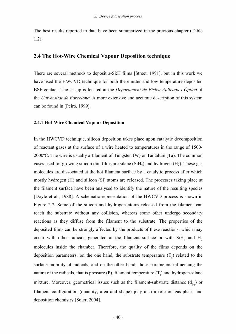
In the HWCVD technique, silicon deposition takes place upon catalytic decomposition
of reactant gases at the surface of a wire heated to temperatures in the range of 1500-
2000ºC. The wire is usually a filament of Tungsten (W) or Tantalum (Ta). The common
gases used for growing silicon thin films are silane (SiH4) and hydrogen (H2). These gas
molecules are dissociated at the hot filament surface by a catalytic process after which
mostly hydrogen (H) and silicon (Si) atoms are released. The processes taking place at
the filament surface have been analysed to identify the nature of the resulting species
[Doyle et al., 1988]. A schematic representation of the HWCVD process is shown in
Figure 2.7. Some of the silicon and hydrogen atoms released from the filament can
reach the substrate without any collision, whereas some other undergo secondary
reactions as they diffuse from the filament to the substrate. The properties of the
deposited films can be strongly affected by the products of these reactions, which may
occur with other radicals generated at the filament surface or with SiH4 and H2
molecules inside the chamber. Therefore, the quality of the films depends on the
deposition parameters: on the one hand, the substrate temperature (Ts) related to the
surface mobility of radicals, and on the other hand, those parameters influencing the
nature of the radicals, that is pressure (P), filament temperature (Tf) and hydrogen-silane
mixture. Moreover, geometrical issues such as the filament-substrate distance (df-s) or
filament configuration (quantity, area and shape) play also a role on gas-phase and
deposition chemistry [Soler, 2004].
2. Device fabrication process
- 41 -
Gas fluxSiH4 + H2
Wire1500ºC- 2000ºC
Secondary reactionsSi+ H + SiH3 +SiH2
Substrate
Gas inlet
Gas fluxSiH4 + H2
Wire1500ºC- 2000ºC
Secondary reactionsSi+ H + SiH3 +SiH2
Substrate
Gas inlet
Figure 2.7: Schematic representation of the processes involved in the HWCVD technique.
2.4.2 The Universitat de Barcelona HWCVD set-up
The HWCVD set-up placed at the Universitat de Barcelona consists of three ultra-high
vacuum chambers isolated by gate valves, as it is shown in figure 2.7. A magnetic
transfer system is used to place the substrate in the desired chamber. The first chamber
is devoted to deposit only undoped a-Si:H films using silane and hydrogen as precursor
gases. Therefore, the intrinsic character of the layer is insured avoiding cross
contamination. Unintentional doping can be specially detrimental when dealing with µc-
Si:H films [Voz et al., 2000], [Song et al., 2000]. The second chamber is intended for
depositing doped layers. Diborane (B2H6) and phosphine (PH3) gases are the doping
precursors added to silane and hydrogen to obtain p- and n-doped layers, respectively.
Finally, the third one is a load-lock chamber to minimize the presence of air in the
HWCVD process chambers. This last chamber also includes an RF magnetron
sputtering cathode to deposit transparent conductive oxides. The inline configuration
allows the deposition of several layers without exposing the samples to the atmosphere.
This possibility is interesting for heterojunction structures based on stacks of an
intrinsic buffer followed by a doped layer. The pumping system consists of a
turbomolecular pump followed by a roots blower pump and a rotary vane pump, which
allow a base pressure below 10-8 mbar in the HWCVD chambers.
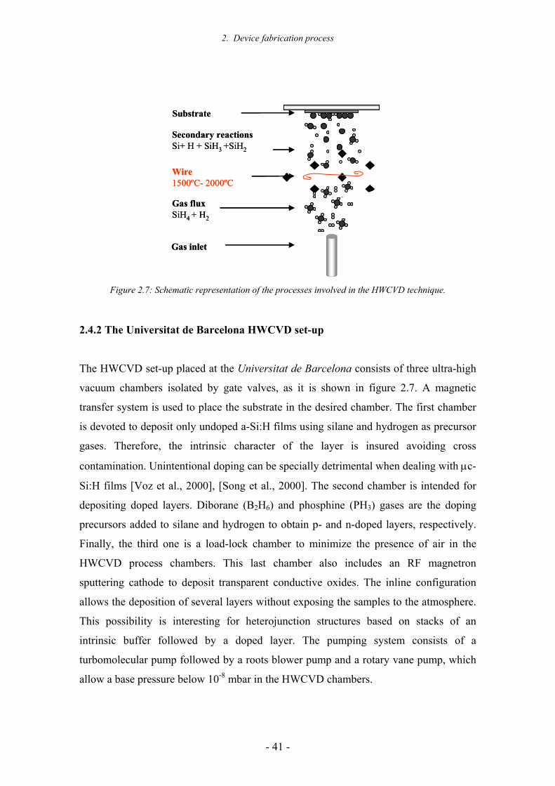
2. Device fabrication process
- 42 -
Figure 2.8: Picture of the multichamber HWCVD set-up. The system was ensembled by the Scientific-
Technical Services of Universitat de Barcelona.
capacitive gauge
heater
shutter wire
thermocouple
pumps
feedgas
substrate
current feedthrough
butterfly valve
penning gauge
Figure 2.9: Internal arrangement of the different components inside the HWCVD chamber.
Figure 2.9 shows a schematic of the configuration inside one of the HWCVD process
chambers (both are similar). Butterfly valves are used to control the process pressure
during thin film deposition. Finally, the substrate temperature is controlled with a
resistive heater, which in the chamber for intrinsic material is external to minimize
unwanted contamination [Fonrodona, 2003]. It is important to remark that the actual
substrate temperature Ts is significantly affected by the wire irradiation, but a previous
calibration has taken into account this influence [Soler, 2004].
2. Device fabrication process
- 43 -
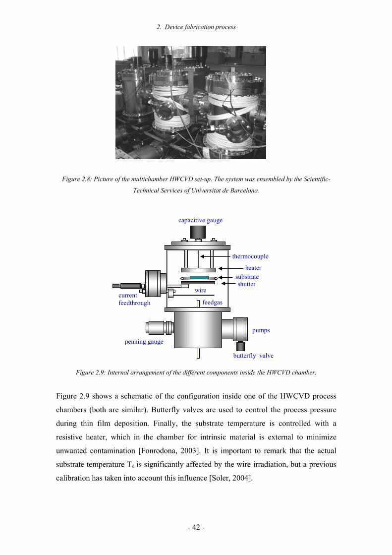
2.4.3 About the wire
In this work, we have mainly used tantalum (Ta) wires with temperatures ranging from
1500 to 1900ºC. Tantalum is a especially suitable catalytic material for low filament
temperatures (Tf) because the formation of silicides on its surface is lower than on
tungsten (W) filaments [Van Veenendaal et al., 2001]. The undesired formation of
silicides increases the filament fragility and its probability of breakage, especially at the
cold ends of the filament [Mahan 2003], [Ishibashi 2001]. Therefore, Ta filaments are a
good alternative to W ones considering their longer lifetime and the better
reproducibility of the process [Van Veen, 2003]. In particular, two different wire
configurations have been considered in this work (Table 2.1).
wire
(material)
∅
(mm)
distance between
wires (cm)
distance to
target (cm)
distance to
gas inlet (cm)
Configuration 1 1 (Ta) 1 X 4 1
Configuration 2 2 (Ta) 0.5 3 4 1
Table 2.1: Parameters of the two different wire configurations used in this work.
The first configuration with one Ta wire of diameter 1mm was the usual configuration
in the HWCVD set-up at Universitat de Barcelona. The second configuration with two
Ta wires was implemented during this thesis to enlarge the homogeneous deposition
area to 4×4 cm2. In this case, two parallel tantalum wires separated 3 cm each other are
centred 1 cm above the gas inlet. The diameter of the wires is 0.5 mm and the distance
to the substrate is 4 cm, as in the single wire configuration.
Figure 2.10: Tantalum wire during a HWCVD process.
2. Device fabrication process
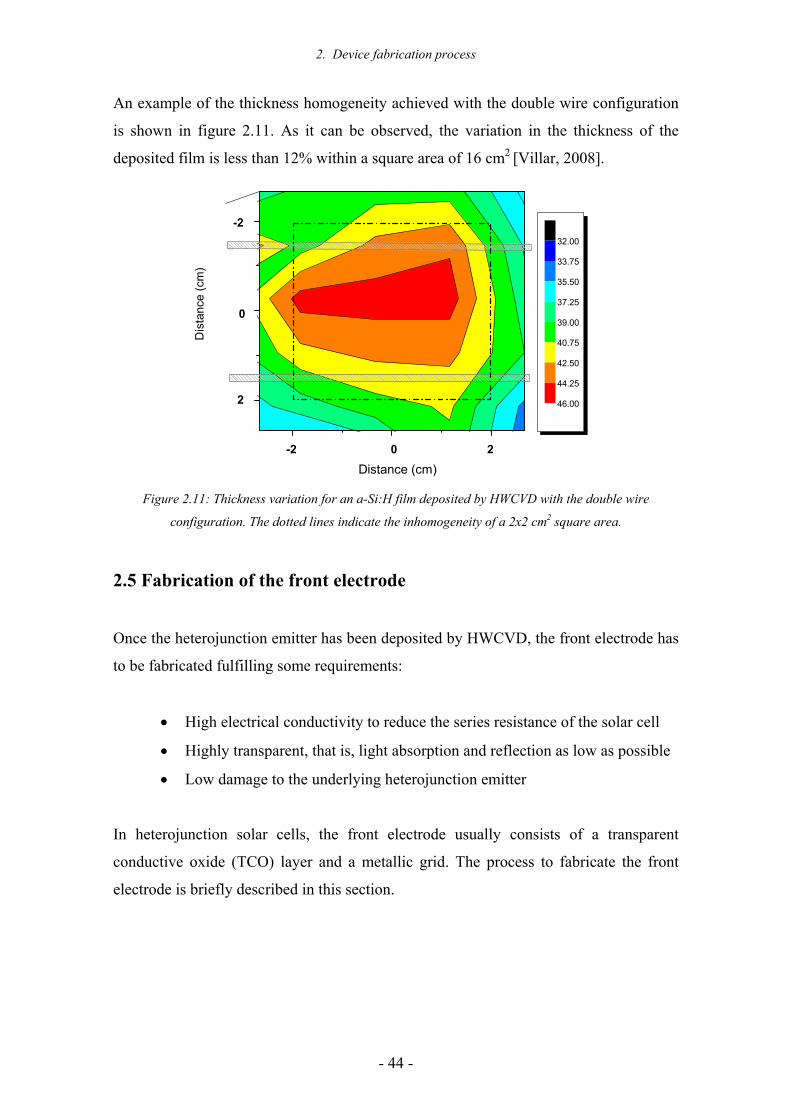
- 44 -
An example of the thickness homogeneity achieved with the double wire configuration
is shown in figure 2.11. As it can be observed, the variation in the thickness of the
deposited film is less than 12% within a square area of 16 cm2 [Villar, 2008].
-2 0 2
-2
2
Dis
tanc
e (c
m)
0
Distance (cm)
32.00
33.75
35.50
37.25
39.00
40.75
42.50
44.25
46.00
Figure 2.11: Thickness variation for an a-Si:H film deposited by HWCVD with the double wire
configuration. The dotted lines indicate the inhomogeneity of a 2x2 cm2 square area.
2.5 Fabrication of the front electrode
Once the heterojunction emitter has been deposited by HWCVD, the front electrode has
to be fabricated fulfilling some requirements:
• High electrical conductivity to reduce the series resistance of the solar cell
• Highly transparent, that is, light absorption and reflection as low as possible
• Low damage to the underlying heterojunction emitter
In heterojunction solar cells, the front electrode usually consists of a transparent
conductive oxide (TCO) layer and a metallic grid. The process to fabricate the front
electrode is briefly described in this section.
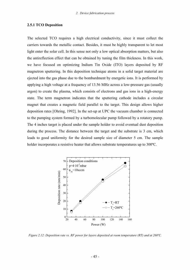
2. Device fabrication process
- 45 -
2.5.1 TCO Deposition
The selected TCO requires a high electrical conductivity, since it must collect the
carriers towards the metallic contact. Besides, it must be highly transparent to let most
light enter the solar cell. In this sense not only a low optical absorption matters, but also
the antireflection effect that can be obtained by tuning the film thickness. In this work,
we have focused on optimizing Indium Tin Oxide (ITO) layers deposited by RF
magnetron sputtering. In this deposition technique atoms in a solid target material are
ejected into the gas phase due to the bombardment by energetic ions. It is performed by
applying a high voltage at a frequency of 13.56 MHz across a low-pressure gas (usually
argon) to create the plasma, which consists of electrons and gas ions in a high-energy
state. The term magnetron indicates that the sputtering cathode includes a circular
magnet that creates a magnetic field parallel to the target. This design allows higher
deposition rates [Ohring, 1992]. In the set-up at UPC the vacuum chamber is connected
to the pumping system formed by a turbomolecular pump followed by a rotatory pump.
The 4 inches target is placed under the sample holder to avoid eventual dust deposition
during the process. The distance between the target and the substrate is 3 cm, which
leads to good uniformity for the desired sample size of diameter 5 cm. The sample
holder incorporates a resistive heater that allows substrate temperatures up to 300ºC.
20 40 60 80 100 120 140 1600
10
20
30
40
50
60
70
Dep
ositi
on ra
te (n
m/m
in)
Power (W)
Ts=RT Ts=260ºC
Deposition conditionsp=4·10-3mbarφAr=10sccm
Figure 2.12: Deposition rate vs. RF power for layers deposited at room temperature (RT) and at 260ºC.
2. Device fabrication process
- 46 -
The ITO layers must be optimized in terms of transparency and conductivity. The
influence of the main deposition parameters has been studied: RF power, substrate
temperature, process pressure, and oxygen and argon flow. Especially remarkable is the
dependence of the deposition rate on the RF power. This curve is shown in figure 2.12
for samples deposited at room temperature (RT) and at 260ºC, over the ITO
crystallisation temperature (~ 250ºC). The influence of other parameters on the
deposition rate has been widely described in the literature [Maissell et al., 1970].
In the case of heterojunction solar cells, changes induced by the ITO deposition process
on the previously deposited a-Si:H layers are also relevant [Christensen et al., 2006].
Then, the optimization process should consider not only the properties of the ITO layer,
but also of the complete heterojunction emitter.
The work function (WF) of the ITO layer is a particularly important parameter to take
into account. The WF value changes with the oxygen concentration and the deposition
temperature [Ulyashin et al., 2002]. Besides deposition conditions, post-treatments like
ozone atmosphere cleaning (UVO) and post-annealing of the samples can shift the work
function from around 4.2 eV up to 5.4 eV [Sugiyama et al., 2000], [Minami, 1999].
Since the a-Si:H layers are very thin, the ITO layer modifies the built in potential of the
device. Lower WF values for (n)a-Si:H [Stangl et al., 2003] and higher ones for (p)a-
Si:H are desired to obtain higher open circuit voltages in the device. For instance, a too
low WF value of the ITO layer on (p)a-Si:H induces the formation of an inverted
Schottky junction that can reduce or even cancel out the device performance [Centurioni
et al., 2003].
2.5.2 Active Area Definition
The active area of the solar cell can be defined either by a lithographic process or, more
simply, by using a shadow mask during the deposition of the ITO layer. In any case, the
surrounding highly doped a-Si:H layer must be etched to isolate the device. Otherwise,
leakage currents reduce the parallel resistance (Rp) of the solar cell leading to degraded
fill factor and open-circuit voltage values [Puigdollers, 1995]. In this thesis two
different etching procedures have been investigated:
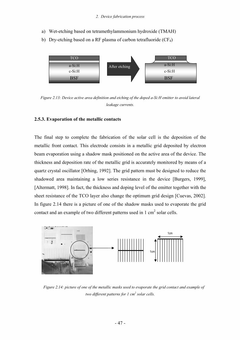
2. Device fabrication process
- 47 -
a) Wet-etching based on tetramethylammonium hydroxide (TMAH)
b) Dry-etching based on a RF plasma of carbon tetrafluoride (CF4)
Figure 2.13: Device active area definition and etching of the doped a-Si:H emitter to avoid lateral
leakage currents.
2.5.3. Evaporation of the metallic contacts
The final step to complete the fabrication of the solar cell is the deposition of the
metallic front contact. This electrode consists in a metallic grid deposited by electron
beam evaporation using a shadow mask positioned on the active area of the device. The
thickness and deposition rate of the metallic grid is accurately monitored by means of a
quartz crystal oscillator [Orhing, 1992]. The grid pattern must be designed to reduce the
shadowed area maintaining a low series resistance in the device [Burgers, 1999],
[Altermatt, 1998]. In fact, the thickness and doping level of the emitter together with the
sheet resistance of the TCO layer also change the optimum grid design [Cuevas, 2002].
In figure 2.14 there is a picture of one of the shadow masks used to evaporate the grid
contact and an example of two different patterns used in 1 cm2 solar cells.
Figure 2.14: picture of one of the metallic masks used to evaporate the grid contact and example of
two different patterns for 1 cm2 solar cells.
a-Si:H c-Si:H
a-Si:H c-Si:H
TCO
After etching
TCO
BSF BSF
1cm
1cm
2. Device fabrication process
- 48 -
In the case of using a low temperature deposited (p+)a-Si:H layer to replace traditional
Al-BSF contacts, also a continuous metallic layer must be deposited at the back side. In
this case a TCO layer is also usually intercalated between the (p+)a-Si:H layer and the
back metallic electrode to reduce the contact resistance and improve the internal back
reflection. In this work different metals have been evaporated in order to evaluate the
contact resistance and adherence with the TCO layer. In the case of ITO, silver seemed
to be the best option.
3. Characterization tools
- 49 -
Chapter 3: Characterization tools
“Demuestra lo que dices y dí lo que demuestras”
(Anónimo)
3.1 Material Characterization tools
In the following sections we summarize the structural and compositional
characterisation tools used in this work to determine the properties of a-Si:H layers. The
electrical and optical characterizations are also considered for films and complete
devices. Here we will briefly describe the experimental set-up, whereas more details on
the results are presented in next chapters.
3.1.1 Structural and compositional characterization
The first measurement carried out for each deposited layer is the measurement of its
thickness by means of a Dektak 3030 stylus profilometer. Then, the growth rate (rd) can
be evaluated considering the deposition time.
a) Raman spectroscopy
Raman spectroscopy is used to evaluate the crystalline fraction (Xc’) of the samples.
The spectrometer was a Jobin-Yvon T64000 with a laser beam at a wavelength of 514
cm-1. The characteristic peak corresponding to the transverse optical (TO) mode of
crystalline silicon can be found at 520 cm-1, whereas the amorphous band appears
around 480 cm-1. The Xc’ can be determined by deconvoluting the amorphous and
microcrystalline contributions using the formula [Tsu et al., 1982]:
3. Characterization tools
- 50 -
ac
cc II
IXσ+
='
_ _
where Ic corresponds to the microcrystalline and Ia to the amorphous intensity
contributions. The parameter σ is the cross section ratio for the Raman effect in a-Si:H
and µc-Si:H and strongly depends on the crystallite size [Bustarret et al., 1988].
Different groups [Han et al., 2003], [Van Veen, 2003] consider additional peaks centred
between 500 and 510 cm-1, mainly attributed to small grain and boundaries effects.
In our case, instead of using the crystalline fraction, we use the crystalline ratio or
integrated crystalline fraction Xc defined as:
480520
520
IIIX c +
=
where I520 and I480 are the intensities of the peaks located at 520 cm-1 and 480 cm-1,
respectively. This simplified parameter is commonly used as an estimation of the real
crystallinity. In order to facilitate comprehension, in next chapters we will refer to Xc as
crystalline fraction.
b) Fourier Transform Infrared (FTIR) Spectroscopy
Fourier Transform Infra-Red Transmittance of silicon thin layers was measured by
means of a Nicolet 5ZDX FTIR spectrometer. This measurement gives us information
related to the concentration of bonded hydrogen atoms and their bonding configuration
in the layer. The infrared wavelength is absorbed in a resonant way by the vibration
modes of the molecules in the layer. The frequency of this vibration allows us to know
the current absorber molecule. The hydrogen can be presented in different
configurations: located interstitially, molecular and forming aggregations, as it is shown
in figure 3.1 [Kail, 2005].
(3.1)
(3.2)
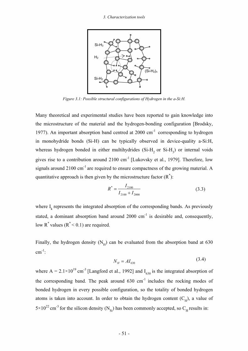
3. Characterization tools
- 51 -
Figure 3.1: Possible structural configurations of Hydrogen in the a-Si:H.
Many theoretical and experimental studies have been reported to gain knowledge into
the microstructure of the material and the hydrogen-bonding configuration [Brodsky,
1977). An important absorption band centred at 2000 cm-1
corresponding to hydrogen
in monohydride bonds (Si-H) can be typically observed in device-quality a-Si:H,
whereas hydrogen bonded in either multihydrides (Si-H2 or Si-H3) or internal voids
gives rise to a contribution around 2100 cm-1 [Lukovsky et al., 1979]. Therefore, low
signals around 2100 cm-1 are required to ensure compactness of the growing material. A
quantitative approach is then given by the microstructure factor (R*):
20002100
2100*
IIIR
+=
where Ik represents the integrated absorption of the corresponding bands. As previously
stated, a dominant absorption band around 2000 cm-1 is desirable and, consequently,
low R* values (R* < 0.1) are required.
Finally, the hydrogen density (NH) can be evaluated from the absorption band at 630
cm-1:
630AINH =
where A = 2.1×1019 cm-3 [Langford et al., 1992] and I630 is the integrated absorption of
the corresponding band. The peak around 630 cm-1 includes the rocking modes of
bonded hydrogen in every possible configuration, so the totality of bonded hydrogen
atoms is taken into account. In order to obtain the hydrogen content (CH), a value of
5×1022 cm-3
for the silicon density (NSi) has been commonly accepted, so CH results in:
H2
Si-H2
Si-H3
(Si-H2)n
(3.4)
(3.3)
3. Characterization tools
- 52 -
%100 atNN
NCSiH
HH ×
+=
Additionally, the incorporation of oxygen in silicon thin films can be detected by the
presence of an absorption band around 1100 cm-1 associated to Si-O bonds [Curtins et
al., 1986].
c) Secondary Ion Mass Spectroscopy (SIMS)
Secondary Ion Mass Spectroscopy is used to analyze the composition of the samples.
Depth profiles of silicon, doping atoms and contaminants have been obtained with an
ATOMIKA 3000-30 ion microprobe system. This destructive technique is based in the
extraction of the material by sputtering the samples with Ar or O ions and the analysis
of the positive secondary ions collected with a mass spectrometer. Thereby, the
concentration profiles of the elements constituting the layer are obtained with a
detection level in parts per million.
3.1.2 Optical and electrical characterization
a) Transmittance / Reflectance
Transmittance measurements of a-Si:H layers deposited on glass were done with an
EPP2000 Spectrometer in the visible and near-infrared wavelength range (λ = 400 -
1200 nm). The measured spectrum indicates the fraction of light transmitted by the
sample. The analysis of transmittance curves allows determining the optical gap (Eg)
according to Tauc’s law [Tauc, 1974] and the thickness of the sample considering the
interference pattern [Swanepoel, 1983].
Moreover, the reflectance of ITO layers was measured with the same set-up using an
optic fibre in T-configuration. Reflectance spectra before and after depositing the front
metallic grid evaluate losses due to shadowing by the front contact.
(3.5)
3. Characterization tools
- 53 -
b) Photothermal Deflection Spectroscopy (PDS)
The optical absorption of a-Si:H layers was measured using the Photothermal
Deflection Spectroscopy (PDS) technique. The basic phenomenon studied in the PDS
technique is the deflection of a light beam when it travels through a medium with an
induced gradient in its refractive index [Boccara et al., 1979]. In our case, the layer
under study is submerged into a liquid (Fluorinert FC72TM by 3M in our set-up), whose
refractive index exhibits a clear thermal dependence. A monochromator is used to select
the wavelength of the radiation reaching the sample, which absorbs a fraction of the
incident light. The absorbed light induces a heating of the sample by non - radiative
recombination. The increasing temperature of the layer causes a temperature gradient in
the liquid, so the refractive index also experiences a variation. This gradient leads to the
deflection of a laser beam which can be quantified by means of the corresponding
detector. A detailed description of the experimental set-up and the calculation of the
optical absorption coefficient (α) can be obtained from [Voz, 2000].
The most relevant characteristic of PDS is its high sensitivity allowing the detection of
very low optical absorption levels (αd < 10-5). Then, PDS complements standard
transmission measurements to obtain the optical absorption spectrum in the whole
visible and near infrared range. Typical spectra for c-Si, µc-Si:H and a-Si:H samples are
described in [Voz, 2000]. Parameters as the optical band gap and the subgap defect
density can be obtained from the treatment of the optical absorption spectra [Soler,
2004].
3.2 Characterization of solar cell precursors
3.2.1 Spectroscopic Phase Modulated Ellipsometry in the UV-visible
Ellipsometry is a sensitive technique used to determine optical properties of surfaces
and thin films. In an ellipsometry measurement we analyze the change in the
polarization of monochromatic light after being reflected on the polished surface of the
sample. Two main properties make this technique very useful in different areas (thin
films, interface properties, roughness analysis…): data are easily obtained and it is a
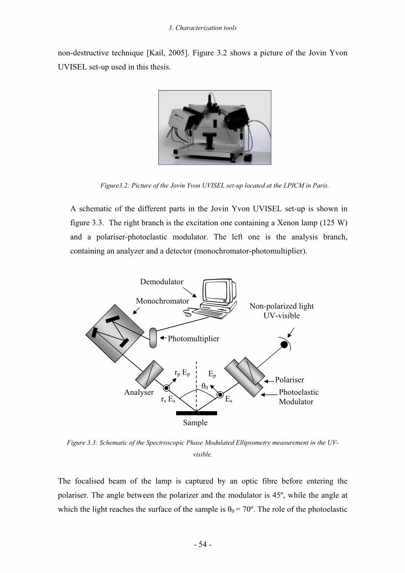
3. Characterization tools
- 54 -
non-destructive technique [Kail, 2005]. Figure 3.2 shows a picture of the Jovin Yvon
UVISEL set-up used in this thesis.
Figure3.2: Picture of the Jovin Yvon UVISEL set-up located at the LPICM in Paris.
A schematic of the different parts in the Jovin Yvon UVISEL set-up is shown in
figure 3.3. The right branch is the excitation one containing a Xenon lamp (125 W)
and a polariser-photoelastic modulator. The left one is the analysis branch,
containing an analyzer and a detector (monochromator-photomultiplier).
Figure 3.3: Schematic of the Spectroscopic Phase Modulated Ellipsometry measurement in the UV-
visible.
The focalised beam of the lamp is captured by an optic fibre before entering the
polariser. The angle between the polarizer and the modulator is 45º, while the angle at
which the light reaches the surface of the sample is θ0 = 70º. The role of the photoelastic
Sample
θ0
rp Ep
rs Es Es
Ep
Analyser
Polariser
Photoelastic Modulator
Photomultiplier
Monochromator
Demodulator
Non-polarized light UV-visible
3. Characterization tools
- 55 -
modulator is to change the polarization state while introducing a time lag between Ep
and Es. To achieve this, a silica bar (with high refraction index) with a piezoelectric
crystal is placed in the modulator. The modulation frequency is 50 kHz, the same as the
silica bar resonance frequency. After the reflexion in the sample, the polarization state
of the beam is analysed by another polarizer similar to the first one. Therefore, the
coefficients rp and rs are obtained. After the analyser, the light is guided through an optic
fibre to the monochromator (filter) and then detected by the photomultiplier. The entire
left branch is equipped with stepping motors controlled by the computer [Kahl, 2005].
The change in the polarization state of the incident and reflected beams is determined by
two angles named ∆ and Ψ. These angles can be related to all the physical parameters of
the sample (thickness, refraction index, absorption coefficient, roughness…).
a) The Models
Ellipsometry is based on the measurement of the pseudo-dielectric function <ε> of the
material. In the case of semi-infinite materials (thick enough to allow photon absorption
before arriving to the substrate) with a polished surface, <ε> is given by:
( ) ( ) ( )ωεωεθρρθωε 210
22
02 tan
111sin i+=
+−
+=
where ρ is obtained from the measurement of the reflection coefficients rp and rs, which
are related to the angles ∆ and Ψ as:
)exp()tan( ∆Ψ== irr
s
pρ
It is especially interesting to analyse the imaginary part of the dielectric function <ε2>
because in absence of phonons only transitions between the valence and the conduction
band affect this term [Van Hove, 1974]. Figure 3.4 shows the imaginary part of the
pseudo-dielectric function for c-Si, a-Si:H and µc-Si:H samples [Aspnes et al., 1984],
[Jellison et al., 1993].
(3.6)
(3.7)
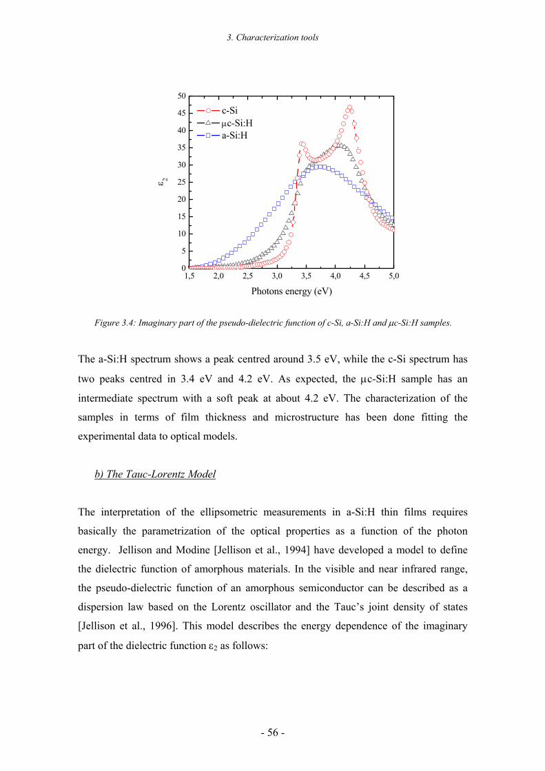
3. Characterization tools
- 56 -
1,5 2,0 2,5 3,0 3,5 4,0 4,5 5,00
5
10
15
20
25
30
35
40
45
50
ε 2
Photons energy (eV)
c-Si µc-Si:H a-Si:H
Figure 3.4: Imaginary part of the pseudo-dielectric function of c-Si, a-Si:H and µc-Si:H samples.
The a-Si:H spectrum shows a peak centred around 3.5 eV, while the c-Si spectrum has
two peaks centred in 3.4 eV and 4.2 eV. As expected, the µc-Si:H sample has an
intermediate spectrum with a soft peak at about 4.2 eV. The characterization of the
samples in terms of film thickness and microstructure has been done fitting the
experimental data to optical models.
b) The Tauc-Lorentz Model
The interpretation of the ellipsometric measurements in a-Si:H thin films requires
basically the parametrization of the optical properties as a function of the photon
energy. Jellison and Modine [Jellison et al., 1994] have developed a model to define
the dielectric function of amorphous materials. In the visible and near infrared range,
the pseudo-dielectric function of an amorphous semiconductor can be described as a
dispersion law based on the Lorentz oscillator and the Tauc’s joint density of states
[Jellison et al., 1996]. This model describes the energy dependence of the imaginary
part of the dielectric function ε2 as follows:
3. Characterization tools
- 57 -
( )( ) g
g EEEECEE
EECEAE >⋅
+−
−= ,1)(
22220
2
20
2ε
The four parameters of this law offer valuable information about the structure of the
material: the optical gap Eg (eV), the factor A (eV) related to the density of the
material, the position of the peak in the spectrum defined by E0 (eV) and, finally, the
disorder factor C (eV).
c) Effective medium theory
We have used the effective medium theory to model stacks of several layers and also in
the case of heterogeneous layers. In this case, the effective medium theory is only
applicable if the dimension of the crystallites into the amorphous phase is smaller than
the wavelength used in the analysis. Otherwise, for bigger dimensions the model cannot
be used because diffusion and diffraction phenomena of the incident light should be
taken into account.
The effective medium theory is based on the addition of the polarization effects. Then,
the effective pseudo-dielectric function of the sample <εeff> is obtained from the
pseudo-dielectric functions <εi> of the constituent materials and their volumetric
fractions, fi [Ayral et al., 2006]:
ai
ai
ii
aeff
aeff
pf
p εεεε
εεεε
−−
=−
−∑
where <εa> is the pseudo-dielectric function of the amorphous phase and p is a
coefficient that depends on the geometry of the inclusions (p = 2 if we consider them
spherical). In particular, the Bruggemann’s approximation [Bruggemann, 1935]
considers symmetrical the amorphous phase and the inclusions, so equation (3.9) can be
rewritten as:
02
=−
−∑
effi
effi
iif εε
εε
(3.8)
(3.9)
(3.10)
3. Characterization tools
- 58 -
A good example of the application of this model are µc-Si:H layers [Fontcuberta, 2004].
The effective pseudo-dielectric function is then an adjusted linear combination of an
amorphous phase <εa> obtained with the Tauc-Lorenz model, microcrystalline phases
<εlg> (little grain) and <εbg> (big grain) obtained from the Jellison models [Jellison,
1993] and a void fraction <εv>. Pseudo-dielectric functions for other materials can be
obtained from [Palik, 1991].
3.2.2 The QSSPC technique
The Quasi-Steady State Photoconductance Technique (QSSPC) is probably the most
common technique to measure the passivating properties of thin films deposited on
crystalline silicon. In heterojunction solar cells both bulk and surface recombination
mechanisms must be considered. While bulk recombination directly depends on the
quality of the c-Si substrate, surface recombination is determined by the passivation
quality at the interfaces in the device. Any recombination process U can be associated to
its characteristic lifetime:
Un∆
=τ (3.11)
where ∆n=n-no is the excess minority carrier density (no is the carrier density under
thermodynamical equilibrium).
a) Bulk recombination in c-Si
In the bulk of c-Si wafers, the lifetime is given by the effect of three main
recombination processes: radiative, Auger and Shockley-Read-Hall recombination:
bSRHAugRadSRHAugRad
nnnnUUUUττττ∆
=∆
+∆
+∆
=++=
In radiative recombination an electron of the conduction band neutralises a hole in the
valence band emitting a photon whose energy corresponds to the semiconductor band
gap [Green, 1982]. Since silicon has an indirect band gap, this process is almost
negligible compared to the other ones.
(3.12)
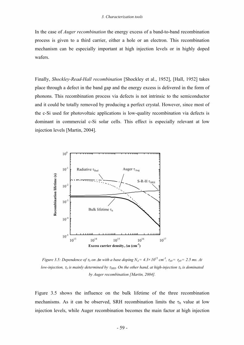
3. Characterization tools
- 59 -
In the case of Auger recombination the energy excess of a band-to-band recombination
process is given to a third carrier, either a hole or an electron. This recombination
mechanism can be especially important at high injection levels or in highly doped
wafers.
Finally, Shockley-Read-Hall recombination [Shockley et al., 1952], [Hall, 1952] takes
place through a defect in the band gap and the energy excess is delivered in the form of
phonons. This recombination process via defects is not intrinsic to the semiconductor
and it could be totally removed by producing a perfect crystal. However, since most of
the c-Si used for photovoltaic applications is low-quality recombination via defects is
dominant in commercial c-Si solar cells. This effect is especially relevant at low
injection levels [Martin, 2004].
Excess carrier density, ∆n (cm-3)
Rec
ombi
natio
n lif
etim
e (s
)
100
10-1
10-2
10-3
1013 1014 1015 1016 1017
Auger τAugRadiative τRad
S-R-H τSRH
Bulk lifetime τb
10-4
10-5
Figure 3.5: Dependence of τb on ∆n with a base doping NA = 4.3×1015 cm-3, τn0 = τp0 = 2.5 ms. At
low-injection, τb is mainly determined by τSRH. On the other hand, at high-injection τb is dominated
by Auger recombination [Martin, 2004].
Figure 3.5 shows the influence on the bulk lifetime of the three recombination
mechanisms. As it can be observed, SRH recombination limits the τb value at low
injection levels, while Auger recombination becomes the main factor at high injection
3. Characterization tools
- 60 -
levels. From now on, we will consider high-injection when ∆n > 10×Ndop and low
injection when 10×ni < ∆n < 10×Ndop, where Ndop is the base doping of the wafer and ni
is the intrinsic carrier density.
b) Surface recombination
A high defect density is expected at the semiconductor surface, since the crystalline
network is completely lost. The defect density is mainly due to dangling bonds, but
additional defects can be created either chemically or mechanically during the
fabrication process of the device. Considering that the units of surface recombination
are (cm-2×s-1), it is more easily described by an effective recombination velocity
measured in (cm×s-1) than by a lifetime. Then, the effective surface recombination
velocity Seff can be defined as [Kim et al., 1980]:
where ∆n is the excess minority carrier density at the limit of the space charge region
created at the c-Si surface.
c) Characterization of the recombination mechanisms
The QSSPC Technique was designed and implemented firstly by R.A. Sinton and A.
Cuevas [Sinton, 1996]. This technique allows the contactless characterization of solar
cell precursors. The system is based on a RF bridge with an inductive coil that generates
electromagnetic fields within the wafer. Variations in the conductivity of the wafer
modify these fields leading to a variation of the effective inductive value, thus changing
the output voltage of the bridge. More details on this technique can be found in [Martin,
2004], [Ferré, 2008].
(3.13)nSU effs ∆= ·
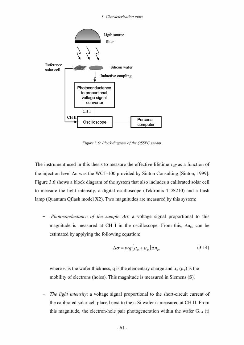
3. Characterization tools
- 61 -
Ligth source
filter
Referencesolar cell Silicon wafer
Photoconductanceto proportional voltage signal
converter
Oscilloscope Personal computer
CH IICH I
Inductive coupling
Ligth source
filter
Referencesolar cell Silicon wafer
Photoconductanceto proportional voltage signal
converter
Oscilloscope Personal computer
CH IICH I
Inductive coupling
Figure 3.6: Block diagram of the QSSPC set-up.
The instrument used in this thesis to measure the effective lifetime τeff as a function of
the injection level ∆n was the WCT-100 provided by Sinton Consulting [Sinton, 1999].
Figure 3.6 shows a block diagram of the system that also includes a calibrated solar cell
to measure the light intensity, a digital oscilloscope (Tektronix TDS210) and a flash
lamp (Quantum Qflash model X2). Two magnitudes are measured by this system:
- Photoconductance of the sample ∆σ: a voltage signal proportional to this
magnitude is measured at CH I in the oscilloscope. From this, ∆nav can be
estimated by applying the following equation:
where w is the wafer thickness, q is the elementary charge and µn (µp) is the
mobility of electrons (holes). This magnitude is measured in Siemens (S).
- The light intensity: a voltage signal proportional to the short-circuit current of
the calibrated solar cell placed next to the c-Si wafer is measured at CH II. From
this magnitude, the electron-hole pair photogeneration within the wafer Gext (t)
( ) avpn nqw ∆+=∆ ··· µµσ (3.14)
3. Characterization tools
- 62 -
can be estimated. To accurately determine Gext(t), it is also necessary to consider
an “effective optical transmission factor” fopt which takes into account the
reflection losses of the sample.
Once these two magnitudes are known, the effective lifetime τeff can be calculated with
the following equation:
)()(
tGtnw
ext
aveff
∆=τ
In the case of a symmetric structure (the same layer deposited on both sides), we can
obtain the effective surface recombination velocity Seff applying:
where τb is the recombination lifetime in the bulk.
A typical τeff vs. ∆nav curve measured by QSSPC is shown in figure 3.7. One important
advantage of this technique compared to other alternatives is the wide irradiance range
(1013 cm-3 - 1017 cm-3) that can be characterized only by changing the filter in the flash
lamp. If high quality c-Si substrates (FZ wafers) are used, the effective lifetime is
actually limited by surface recombination (τb >> τeff). Hence, we usually obtain a good
approximation to the upper limit of the effective surface recombination velocity Seff.
Furthermore, this technique allows the estimation of the implicit open-circuit voltage
Voc of the solar cell precursor:
( )
+
∆+∆= 1ln 2
i
Aoc n
pNnq
kTV (3.18)
For high injection levels (∆p=∆n), the excess carrier densities can be considered equal
to the average excess carrier density measured by QSSPC.
The error in the calculation of τeff by this technique can be considered lower than 15%
taking into account non linearities between photoconductance and the output signal,
maladjustments in the optical factor (fopt) or variations in the flash spectrum, among
other factors [Martin, 2004].
(3.15)
(3.16)eff
effwSτ2
≤w
Seff
beff
211+=
ττ
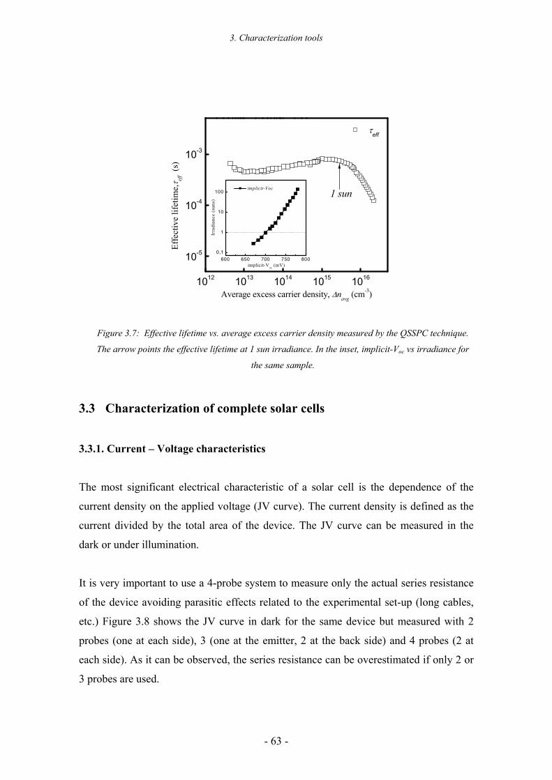
3. Characterization tools
- 63 -
1012 1013 1014 1015 1016
10-5
10-4
10-3
600 650 700 750 8000,1
1
10
100 implicit-Voc
implicit-Voc (mV)
Irra
dian
ce (s
uns)
τeff
Effe
ctiv
e lif
etim
e,τ ef
f (s)
Average excess carrier density, ∆navg (cm-3)
1 sun
Figure 3.7: Effective lifetime vs. average excess carrier density measured by the QSSPC technique.
The arrow points the effective lifetime at 1 sun irradiance. In the inset, implicit-Voc vs irradiance for
the same sample.
3.3 Characterization of complete solar cells
3.3.1. Current – Voltage characteristics
The most significant electrical characteristic of a solar cell is the dependence of the
current density on the applied voltage (JV curve). The current density is defined as the
current divided by the total area of the device. The JV curve can be measured in the
dark or under illumination.
It is very important to use a 4-probe system to measure only the actual series resistance
of the device avoiding parasitic effects related to the experimental set-up (long cables,
etc.) Figure 3.8 shows the JV curve in dark for the same device but measured with 2
probes (one at each side), 3 (one at the emitter, 2 at the back side) and 4 probes (2 at
each side). As it can be observed, the series resistance can be overestimated if only 2 or
3 probes are used.
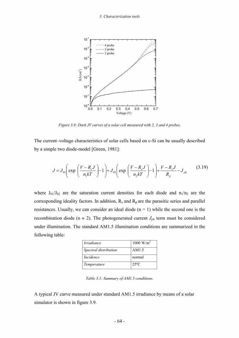
3. Characterization tools
- 64 -
0.0 0.1 0.2 0.3 0.4 0.5 0.6 0.710-8
10-7
10-6
10-5
10-4
10-3
10-2
10-1
J(A
/cm
2 )
Voltage (V)
4 probe 3 probe 2 probe
Figure 3.8: Dark JV curves of a solar cell measured with 2, 3 and 4 probes.
The current–voltage characteristics of solar cells based on c-Si can be usually described
by a simple two diode-model [Green, 1981]:
php
sss JR
JRVkTn
JRVJkTn
JRVJJ −−
+
−
−+
−
−= 1 exp1 exp
202
101
where J01/J02 are the saturation current densities for each diode and n1/n2 are the
corresponding ideality factors. In addition, Rs and Rp are the parasitic series and parallel
resistances. Usually, we can consider an ideal diode (n = 1) while the second one is the
recombination diode (n ≈ 2). The photogenerated current Jph term must be considered
under illumination. The standard AM1.5 illumination conditions are summarized in the
following table: Irradiance 1000 W/m2
Spectral distribution AM1.5
Incidence normal
Temperature 25ºC
Table 3.1: Summary of AM1.5 conditions.
A typical JV curve measured under standard AM1.5 irradiance by means of a solar
simulator is shown in figure 3.9.
(3.19)
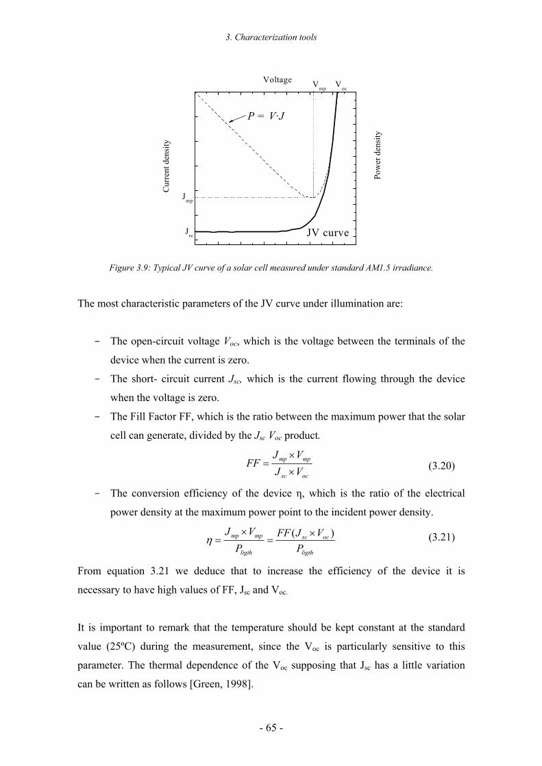
3. Characterization tools
- 65 -
JV curve
Voltage
Cur
rent
den
sity
VocVmp
Jmp
Pow
er d
ensi
ty
Jsc
P = V·J
Figure 3.9: Typical JV curve of a solar cell measured under standard AM1.5 irradiance.
The most characteristic parameters of the JV curve under illumination are:
- The open-circuit voltage Voc, which is the voltage between the terminals of the
device when the current is zero.
- The short- circuit current Jsc, which is the current flowing through the device
when the voltage is zero.
- The Fill Factor FF, which is the ratio between the maximum power that the solar
cell can generate, divided by the Jsc Voc product.
ocsc
mpmp
VJVJ
FF×
×=
- The conversion efficiency of the device η, which is the ratio of the electrical
power density at the maximum power point to the incident power density.
ligth
ocsc
ligth
mpmp
PVJFF
PVJ )( ×
=×
=η
From equation 3.21 we deduce that to increase the efficiency of the device it is
necessary to have high values of FF, Jsc and Voc.
It is important to remark that the temperature should be kept constant at the standard
value (25ºC) during the measurement, since the Voc is particularly sensitive to this
parameter. The thermal dependence of the Voc supposing that Jsc has a little variation
can be written as follows [Green, 1998].
(3.20)
(3.21)
3. Characterization tools
- 66 -
TqkTVV
dTdV ocgooc )/(γ+−
−=
where Vgo is the bandgap (~1.2 eV for c-Si) and γ is a coefficient with value ranging
from 1 to 4. Considering T =300 K with a usual Voc of 0.6 V and γ~3, we obtain:
CmVdT
dVoc /º 3.2−=
which represents a decrease in the Voc of 0.4% per ºC for diffused c-Si solar cells. In the
particular case of heterojunction solar cells the thermal dependence of the Voc is slightly
lower (~ -2 mV/ºC).
3.3.2. Spectral Response
Spectral response (SR) measurements have been performed to get detailed information
about the current generation process in the solar cell. The spectral response is defined as
the amount of current collected Jph by the device per watt of incident light of a given
wavelength (λ) for an external voltage applied V.
),(),(
λλ
VPJ
VSR ph=
The spectral response measurements were performed with a set-up formed by a Xenon
gas lamp followed by a monochromator and also a lock-in amplifier. In order to
measure the spectral power density P (V,λ) reaching the solar cell for each wavelength
we used a calibrated silicon photodetector as a reference.
The External Quantum Efficiency (EQE) can be calculated from the spectral response of
the device offering a more physical meaning. The EQE is defined as the fraction of
incident photons at a wavelength λ transformed into an electron-hole pair collected at
the contacts of the device. The relation between SR and EQE is simply given by:
λλλ 1241),(),( ×= VSRVEQE
(3.23)
(3.22)
(3.24)
(3.25)
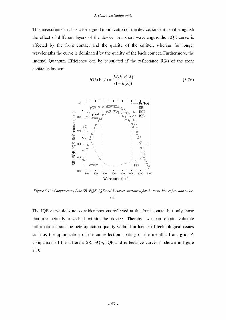
3. Characterization tools
- 67 -
This measurement is basic for a good optimization of the device, since it can distinguish
the effect of different layers of the device. For short wavelengths the EQE curve is
affected by the front contact and the quality of the emitter, whereas for longer
wavelengths the curve is dominated by the quality of the back contact. Furthermore, the
Internal Quantum Efficiency can be calculated if the reflectance R(λ) of the front
contact is known:
))(1(),(),(
λλλ
RVEQEVIQE
−= (3.26)
400 500 600 700 800 900 1000 11000.0
0.2
0.4
0.6
0.8
1.0
BSF
R(ITO) SR EQE IQE
SR, E
QE,
IQE,
Ref
lect
ance
( a.
u.)
Wavelength (nm)
opticallosses
emitter
Figure 3.10: Comparison of the SR, EQE, IQE and R curves measured for the same heterojunction solar
cell.
The IQE curve does not consider photons reflected at the front contact but only those
that are actually absorbed within the device. Thereby, we can obtain valuable
information about the heterojunction quality without influence of technological issues
such as the optimization of the antireflection coating or the metallic front grid. A
comparison of the different SR, EQE, IQE and reflectance curves is shown in figure
3.10.
4. Amorphous and microcrystalline silicon deposited by HWCVD
- 68 -
Chapter 4: Amorphous and
microcrystalline silicon deposited
by HWCVD
“La mejor estructura no garantizará los
resultados ni el rendimiento. Pero la estructura equivocada es una garantía de fracaso”
P. Drucker
In this chapter, the different materials used in this thesis to fabricate heterojunction
silicon solar cells are briefly described. On the one hand, the main properties of thin
silicon films grown by HWCVD are reviewed. On the other hand, the criteria used to
select which materials are better for our devices are discussed. Both the intrinsic
material used in the buffer layer and the doped layers for the emitter and back contact
are considered.
4.1 Between a-Si:H and µc-Si:H
Amorphous silicon (a-Si) is the non-crystalline form of silicon. In its crystalline form,
each silicon atom is bonded to four neighbouring silicon atoms forming a
tetrahedron. Although this is also the case in a-Si, it does not actually form a continuous
crystalline lattice. In amorphous silicon some atoms may have dangling bonds, which
4. Amorphous and microcrystalline silicon deposited by HWCVD
- 69 -
occur when those atoms are not bonded to four neighbouring atoms. These dangling
bonds are defects in the continuous random network, and can be partially passivated by
introducing hydrogen atoms in the material. Then this material becomes hydrogenated
amorphous silicon (a-Si:H), which is actually the form used in electronic applications.
Hydrogenated amorphous silicon is usually referred as amorphous silicon to simplify,
but it must be clear that there must be significant hydrogen content to obtain acceptable
electronic properties.
The beneficial role of hydrogen dilution in PECVD deposited a-Si:H has been widely
accepted since observations of improved stability were first reported [Guha et al., 1981].
Moderate hydrogen dilutions (lower than those used in PECVD) have also led to
reduced defect metastability in a-Si:H obtained by Hot-Wire CVD [Bauer et al., 1998].
Hydrogenated nanocrystalline silicon (nc-Si:H) or microcrystyalline silicon (µc-
Si:H) are allotropic forms of silicon where an amorphous phase coexists with embedded
small grains of crystalline silicon. The difference between nc-Si:H and µc-Si:H comes
solely from the grain size of the crystallites, as is shown in table 4.1. These small-grain
materials can be grown at moderate substrate temperatures [Bergmann, 1999]. By
contrast, polycrystalline silicon (poly-Si) consists only of crystalline silicon grains
separated by grain boundaries. This type of material is usually fabricated at high
substrate temperatures without requirement of added hydrogen.
Symbol Description Feature size a-Si:H single phase amorphous none nc-Si:H two phase amorphous and crystalline <20nm µc-Si:H two phase amorphous and crystalline <1µm poly-Si single phase with grain boundaries >1µm
Table 4.1: Definitions of various morphologies of thin silicon films.
Anyway, the classification attending to the grain size is still controversial and the terms
µc-Si:H and poly-Si:H can be often found in the literature referring to nc-Si:H films.
Furthermore, a variety of thin film silicon materials produced near the onset of
crystallisation, which exhibit very promising properties, have gained interest during the
last years. Thus, polymorphous silicon (pm-Si:H) [Roca i Cabarrocas et al., 1998] or
4. Amorphous and microcrystalline silicon deposited by HWCVD
- 70 -
protocrystalline silicon (pc-Si:H) [Koh et al., 1999], [Fontcuberta i Morral et al., 2001]
are new terms that have been recently introduced into the terminology of thin film
silicon technology.
A possible advantage of nc-Si:H and µc-Si:H over a-Si:H is that higher mobilities can
be usually achieved due to the presence of crystallites. They also show an increased
absorption in the red and infrared wavelength range, which is really relevant in thin film
silicon solar cells. Besides, in part as a consequence of their lower hydrogen content,
these materials are also more stable than a-Si:H. Here we are referring to the stability
against the so called Staebler-Wronski effect [Staebler et al., 1977], because the
chemical stability against oxidation is better in a-Si:H material.
Therefore, the need to control the crystallinity of the layers obtained by Hot-Wire CVD
is clear. For that purpose, we can basically change the hydrogen dilution (CH) and the
substrate temperature (Ts) [Tsu et al., 1997], [Mahan et al., 2000], [Han et al., 2003].
Other technological parameters such as the filament temperature (Tf) or the process
pressure (P) [Soler, 2004] in our HWCVD reactor have also a significant influence in
the crystallinity of the films.
A description of the optoelectronic properties that the different materials used in
heterojunction silicon solar cells should fulfil is presented next. We will use the term
device-quality material to summarize all the basic properties required for the different
layers. Obviously, these properties are different depending on the function of the layer
in the device. We will discuss the intrinsic and doped material separately.
4.2 Device-quality intrinsic amorphous silicon deposited by HWCVD
The interest for good intrinsic amorphous silicon in heterojunction solar cells lies
basically in obtaining a non defective layer with good passivation properties. In
addition, this intrinsic material must allow the current flow through the thin buffer layer
without blocking the electric field. These two premises have been considered for the
optimization of the intrinsic a-Si:H deposited by HWCVD.
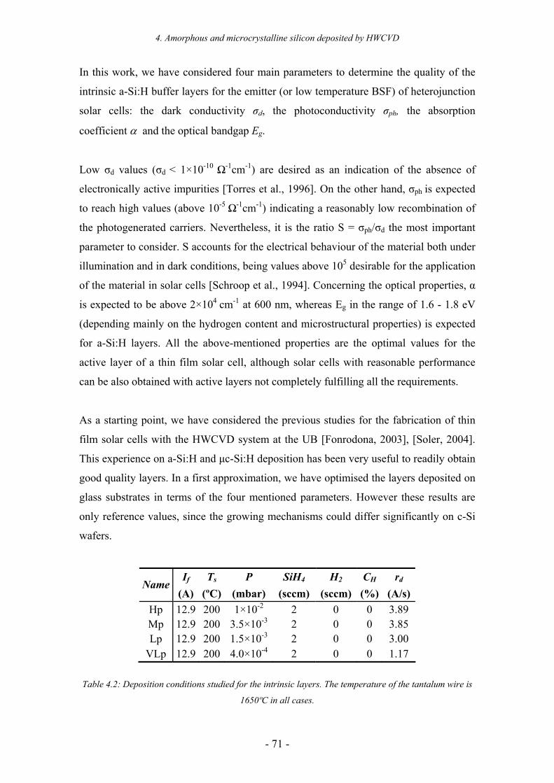
4. Amorphous and microcrystalline silicon deposited by HWCVD
- 71 -
In this work, we have considered four main parameters to determine the quality of the
intrinsic a-Si:H buffer layers for the emitter (or low temperature BSF) of heterojunction
solar cells: the dark conductivity σd, the photoconductivity σph, the absorption
coefficient α and the optical bandgap Eg.
Low σd values (σd < 1×10⁻¹⁰ Ω-1cm-1) are desired as an indication of the absence of
electronically active impurities [Torres et al., 1996]. On the other hand, σph is expected
to reach high values (above 10-5 Ω-1cm-1) indicating a reasonably low recombination of
the photogenerated carriers. Nevertheless, it is the ratio S = σph/σd the most important
parameter to consider. S accounts for the electrical behaviour of the material both under
illumination and in dark conditions, being values above 105 desirable for the application
of the material in solar cells [Schroop et al., 1994]. Concerning the optical properties, α
is expected to be above 2×104 cm-1 at 600 nm, whereas Eg in the range of 1.6 - 1.8 eV
(depending mainly on the hydrogen content and microstructural properties) is expected
for a-Si:H layers. All the above-mentioned properties are the optimal values for the
active layer of a thin film solar cell, although solar cells with reasonable performance
can be also obtained with active layers not completely fulfilling all the requirements.
As a starting point, we have considered the previous studies for the fabrication of thin
film solar cells with the HWCVD system at the UB [Fonrodona, 2003], [Soler, 2004].
This experience on a-Si:H and µc-Si:H deposition has been very useful to readily obtain
good quality layers. In a first approximation, we have optimised the layers deposited on
glass substrates in terms of the four mentioned parameters. However these results are
only reference values, since the growing mechanisms could differ significantly on c-Si
wafers.
If Ts P SiH4 H2 CH rd Name(A) (ºC) (mbar) (sccm) (sccm) (%) (A/s)
Hp 12.9 200 1×10⁻² 2 0 0 3.89 Mp 12.9 200 3.5×10⁻³ 2 0 0 3.85 Lp 12.9 200 1.5×10⁻³ 2 0 0 3.00
VLp 12.9 200 4.0×10⁻⁴ 2 0 0 1.17
Table 4.2: Deposition conditions studied for the intrinsic layers. The temperature of the tantalum wire is
1650ºC in all cases.
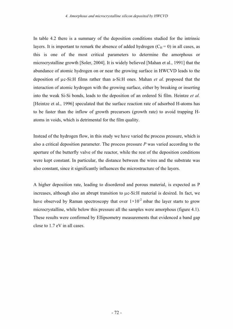
4. Amorphous and microcrystalline silicon deposited by HWCVD
- 72 -
In table 4.2 there is a summary of the deposition conditions studied for the intrinsic
layers. It is important to remark the absence of added hydrogen (CH = 0) in all cases, as
this is one of the most critical parameters to determine the amorphous or
microcrystalline growth [Soler, 2004]. It is widely believed [Mahan et al., 1991] that the
abundance of atomic hydrogen on or near the growing surface in HWCVD leads to the
deposition of µc-Si:H films rather than a-Si:H ones. Mahan et al. proposed that the
interaction of atomic hydrogen with the growing surface, either by breaking or inserting
into the weak Si-Si bonds, leads to the deposition of an ordered Si film. Heintze et al.
[Heintze et al., 1996] speculated that the surface reaction rate of adsorbed H-atoms has
to be faster than the inflow of growth precursors (growth rate) to avoid trapping H-
atoms in voids, which is detrimental for the film quality.
Instead of the hydrogen flow, in this study we have varied the process pressure, which is
also a critical deposition parameter. The process pressure P was varied according to the
aperture of the butterfly valve of the reactor, while the rest of the deposition conditions
were kept constant. In particular, the distance between the wires and the substrate was
also constant, since it significantly influences the microstructure of the layers.
A higher deposition rate, leading to disordered and porous material, is expected as P
increases, although also an abrupt transition to µc-Si:H material is desired. In fact, we
have observed by Raman spectroscopy that over 1×10⁻² mbar the layer starts to grow
microcrystalline, while below this pressure all the samples were amorphous (figure 4.1).
These results were confirmed by Ellipsometry measurements that evidenced a band gap
close to 1.7 eV in all cases.
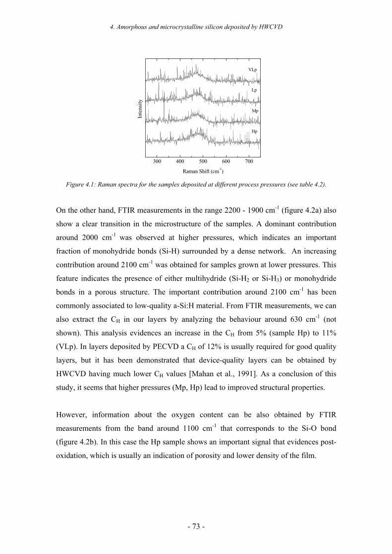
4. Amorphous and microcrystalline silicon deposited by HWCVD
- 73 -
300 400 500 600 700
Hp
Mp
Lp
VLp
Inte
nsity
Raman Shift (cm-1) Figure 4.1: Raman spectra for the samples deposited at different process pressures (see table 4.2).
On the other hand, FTIR measurements in the range 2200 - 1900 cm-1 (figure 4.2a) also
show a clear transition in the microstructure of the samples. A dominant contribution
around 2000 cm-1 was observed at higher pressures, which indicates an important
fraction of monohydride bonds (Si-H) surrounded by a dense network. An increasing
contribution around 2100 cm-1 was obtained for samples grown at lower pressures. This
feature indicates the presence of either multihydride (Si-H2 or Si-H3) or monohydride
bonds in a porous structure. The important contribution around 2100 cm-1 has been
commonly associated to low-quality a-Si:H material. From FTIR measurements, we can
also extract the CH in our layers by analyzing the behaviour around 630 cm-1 (not
shown). This analysis evidences an increase in the CH from 5% (sample Hp) to 11%
(VLp). In layers deposited by PECVD a CH of 12% is usually required for good quality
layers, but it has been demonstrated that device-quality layers can be obtained by
HWCVD having much lower CH values [Mahan et al., 1991]. As a conclusion of this
study, it seems that higher pressures (Mp, Hp) lead to improved structural properties.
However, information about the oxygen content can be also obtained by FTIR
measurements from the band around 1100 cm-1 that corresponds to the Si-O bond
(figure 4.2b). In this case the Hp sample shows an important signal that evidences post-
oxidation, which is usually an indication of porosity and lower density of the film.
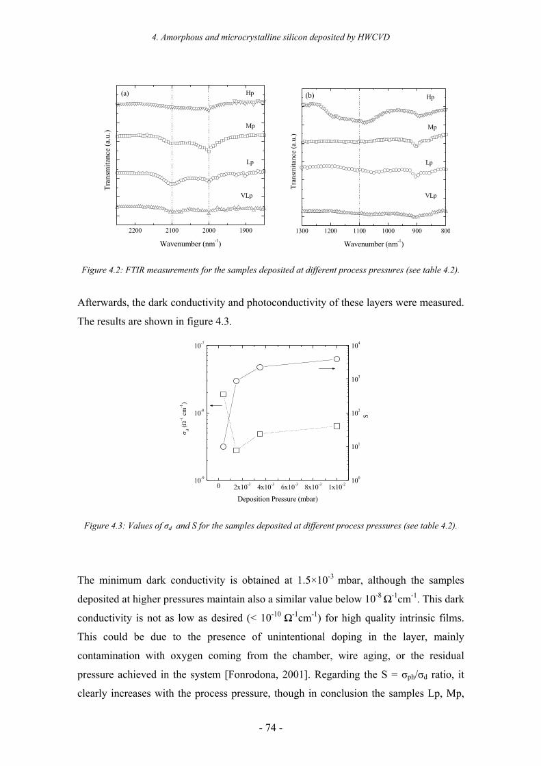
4. Amorphous and microcrystalline silicon deposited by HWCVD
- 74 -
2200 2100 2000 1900
Hp
Mp
Lp
VLp
Tran
smita
nce
(a.u
.)
Wavenumber (nm-1)
(a)
1300 1200 1100 1000 900 800
Hp
Mp
Lp
VLp
Tran
smita
nce
(a.u
.)
Wavenumber (nm-1)
(b)
Figure 4.2: FTIR measurements for the samples deposited at different process pressures (see table 4.2).
Afterwards, the dark conductivity and photoconductivity of these layers were measured.
The results are shown in figure 4.3.
0 2x10⁻³ 4x10⁻³ 6x10⁻³ 8x10⁻³ 1x10-210-9
10-8
10-7
σ d (Ω−1
cm
-1)
Deposition Pressure (mbar)
100
101
102
103
104
S
Figure 4.3: Values of σd and S for the samples deposited at different process pressures (see table 4.2).
The minimum dark conductivity is obtained at 1.5×10⁻³ mbar, although the samples
deposited at higher pressures maintain also a similar value below 10-8 Ω-1cm-1. This dark
conductivity is not as low as desired (< 10-10 Ω-1cm-1) for high quality intrinsic films.
This could be due to the presence of unintentional doping in the layer, mainly
contamination with oxygen coming from the chamber, wire aging, or the residual
pressure achieved in the system [Fonrodona, 2001]. Regarding the S = σph/σd ratio, it
clearly increases with the process pressure, though in conclusion the samples Lp, Mp,
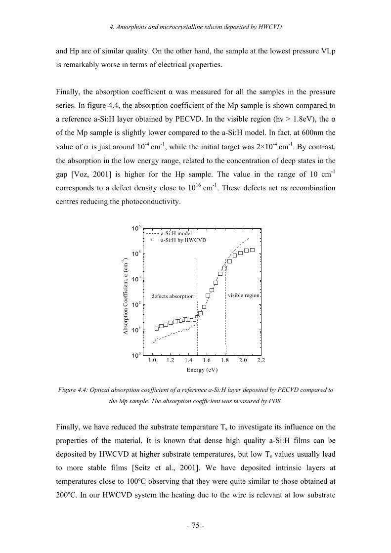
4. Amorphous and microcrystalline silicon deposited by HWCVD
- 75 -
and Hp are of similar quality. On the other hand, the sample at the lowest pressure VLp
is remarkably worse in terms of electrical properties.
Finally, the absorption coefficient α was measured for all the samples in the pressure
series. In figure 4.4, the absorption coefficient of the Mp sample is shown compared to
a reference a-Si:H layer obtained by PECVD. In the visible region (hν > 1.8eV), the α
of the Mp sample is slightly lower compared to the a-Si:H model. In fact, at 600nm the
value of α is just around 10-4 cm-1, while the initial target was 2×10⁻⁴ cm-1. By contrast,
the absorption in the low energy range, related to the concentration of deep states in the
gap [Voz, 2001] is higher for the Hp sample. The value in the range of 10 cm-1
corresponds to a defect density close to 1016 cm-1. These defects act as recombination
centres reducing the photoconductivity.
1.0 1.2 1.4 1.6 1.8 2.0 2.2100
101
102
103
104
105
visible regiondefects absorption
Abs
orpt
ion
Coe
ffic
ient
, α (c
m-1
)
Energy (eV)
a-Si:H model a-Si:H by HWCVD
Figure 4.4: Optical absorption coefficient of a reference a-Si:H layer deposited by PECVD compared to
the Mp sample. The absorption coefficient was measured by PDS.
Finally, we have reduced the substrate temperature Ts to investigate its influence on the
properties of the material. It is known that dense high quality a-Si:H films can be
deposited by HWCVD at higher substrate temperatures, but low Ts values usually lead
to more stable films [Seitz et al., 2001]. We have deposited intrinsic layers at
temperatures close to 100ºC observing that they were quite similar to those obtained at
200ºC. In our HWCVD system the heating due to the wire is relevant at low substrate
4. Amorphous and microcrystalline silicon deposited by HWCVD
- 76 -
temperatures (Ts<200ºC). Hence, the actual temperature could be around 150ºC though
we fixed the substrate heater to only 100ºC. We have also observed that the passivation
quality of the buffer layer is even better when it is deposited at Ts=100ºC and annealed
at 200ºC during the deposition of the doped layer.
In the particular case of heterojunction solar cells, we have to consider also the
differences in the growing process on c-Si substrates. We have observed that the desired
abrupt heterojunction onto the c-Si surface is obtained with the material deposited at
only 3.5×10⁻³ mbar. Then, better materials in terms of conductivity result in total or
partial epitaxy on c-Si (for instance Hp) and they are absolutely discarded for our
application. Moreover, the properties measured in 1 µm-thick a-Si:H layers deposited
on glass (like the ones presented above) are quite difficult to compare with extremely
thin (5 nm) a-Si:H layers on c-Si. For instance, in our case the properties of the buffer
layer can be strongly affected by the deposition of the following doped layer (see
chapter 5). As a conclusion, we can consider that even though our layers do not fulfill
all the device-quality established properties in terms of material, they certainly achieve
all the requirements in terms of passivation and microstructure demanded by
heterojunction devices. This will be evident in the analysis of the solar cell precursors
during the next chapter.
4.3 Doped amorphous & microcrystalline silicon deposited by
HWCVD
In this section we study the optical and electrical properties of both n- and p-type thin
silicon films for heterojunction solar cells. Doping of a-Si:H was first demonstrated by
Spear and LeComber [Spear and LeComber, 1975], who showed the capability to obtain
both p- and n-type material by PECVD. Suitable amounts of either diborane (B2H6) for
p-type material or phosphine (PH3) for n-type layers were added to the gas mixture in
the reactor. This result demonstrated the enormous potential of a-Si:H. The disordered
structure of a-Si:H was supposed to allow the incorporation of dopant atoms into the
amorphous network, thus impeding the doping of the material. Later on, the doping
mechanism of a-Si:H was further clarified by Street [Street, 1991]. Nevertheless, the
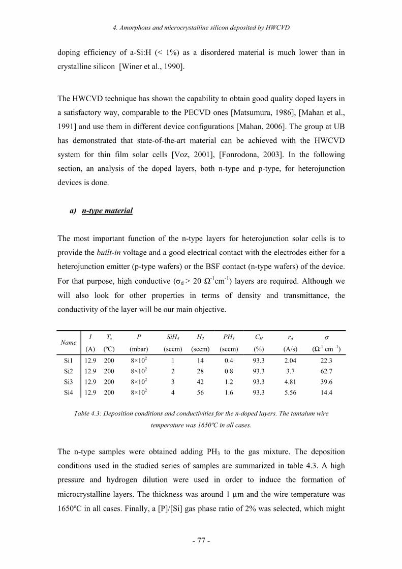
4. Amorphous and microcrystalline silicon deposited by HWCVD
- 77 -
doping efficiency of a-Si:H (< 1%) as a disordered material is much lower than in
crystalline silicon [Winer et al., 1990].
The HWCVD technique has shown the capability to obtain good quality doped layers in
a satisfactory way, comparable to the PECVD ones [Matsumura, 1986], [Mahan et al.,
1991] and use them in different device configurations [Mahan, 2006]. The group at UB
has demonstrated that state-of-the-art material can be achieved with the HWCVD
system for thin film solar cells [Voz, 2001], [Fonrodona, 2003]. In the following
section, an analysis of the doped layers, both n-type and p-type, for heterojunction
devices is done.
a) n-type material
The most important function of the n-type layers for heterojunction solar cells is to
provide the built-in voltage and a good electrical contact with the electrodes either for a
heterojunction emitter (p-type wafers) or the BSF contact (n-type wafers) of the device.
For that purpose, high conductive (σd > 20 Ω-1cm-1) layers are required. Although we
will also look for other properties in terms of density and transmittance, the
conductivity of the layer will be our main objective.
I Ts P SiH4 H2 PH3 CH rd σ Name
(A) (ºC) (mbar) (sccm) (sccm) (sccm) (%) (A/s) (Ω-1 cm -1)
Si1 12.9 200 8×10² 1 14 0.4 93.3 2.04 22.3 Si2 12.9 200 8×10² 2 28 0.8 93.3 3.7 62.7 Si3 12.9 200 8×10² 3 42 1.2 93.3 4.81 39.6 Si4 12.9 200 8×10² 4 56 1.6 93.3 5.56 14.4
Table 4.3: Deposition conditions and conductivities for the n-doped layers. The tantalum wire
temperature was 1650ºC in all cases.
The n-type samples were obtained adding PH3 to the gas mixture. The deposition
conditions used in the studied series of samples are summarized in table 4.3. A high
pressure and hydrogen dilution were used in order to induce the formation of
microcrystalline layers. The thickness was around 1 µm and the wire temperature was
1650ºC in all cases. Finally, a [P]/[Si] gas phase ratio of 2% was selected, which might
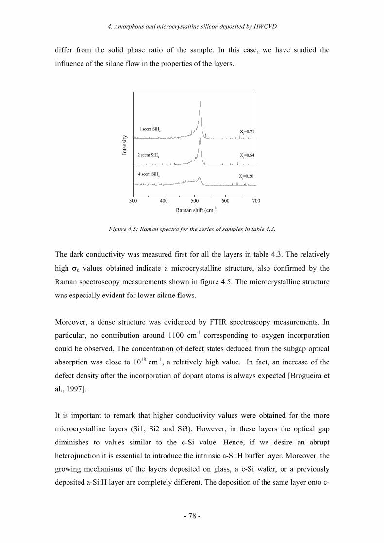
4. Amorphous and microcrystalline silicon deposited by HWCVD
- 78 -
differ from the solid phase ratio of the sample. In this case, we have studied the
influence of the silane flow in the properties of the layers.
300 400 500 600 700
Xc=0.20
Xc=0.71
2 sccm SiH4
4 sccm SiH4
Inte
nsity
Raman shift (cm-1)
1 sccm SiH4
Xc=0.64
Figure 4.5: Raman spectra for the series of samples in table 4.3.
The dark conductivity was measured first for all the layers in table 4.3. The relatively
high σd values obtained indicate a microcrystalline structure, also confirmed by the
Raman spectroscopy measurements shown in figure 4.5. The microcrystalline structure
was especially evident for lower silane flows.
Moreover, a dense structure was evidenced by FTIR spectroscopy measurements. In
particular, no contribution around 1100 cm-1 corresponding to oxygen incorporation
could be observed. The concentration of defect states deduced from the subgap optical
absorption was close to 1018 cm-1, a relatively high value. In fact, an increase of the
defect density after the incorporation of dopant atoms is always expected [Brogueira et
al., 1997].
It is important to remark that higher conductivity values were obtained for the more
microcrystalline layers (Si1, Si2 and Si3). However, in these layers the optical gap
diminishes to values similar to the c-Si value. Hence, if we desire an abrupt
heterojunction it is essential to introduce the intrinsic a-Si:H buffer layer. Moreover, the
growing mechanisms of the layers deposited on glass, a c-Si wafer, or a previously
deposited a-Si:H layer are completely different. The deposition of the same layer onto c-
4. Amorphous and microcrystalline silicon deposited by HWCVD
- 79 -
Si is expected to be more microcrystalline, even producing in some cases an epitaxial
growth. By contrast, on the a-Si:H buffer layer a disordered phase of a few nanometres
is obtained, appearing later the first grains.
Besides, as it happened with the intrinsic buffer, the doped layers used for
heterojunction devices are actually 50-100 times thinner than the samples studied here.
This fact means that although we observe a high crystalline fraction on glass, this value
is expected to be much lower for the thinner films on first stages of grain nucleation
used in solar cells. As we will discuss in the next chapter, only Ellipsometry
measurements performed on the solar cell precursors offer confident information about
the real structure of the layers. Obviously, the conductivity will be also affected by
decreasing the film thickness. Therefore, we have selected only as a starting point the
best n-doped microcrystalline layer (Si2) that will be further optimized in final devices.
Nevertheless, microstructural, optical and electrical requirements for device quality n-
type layers [Schropp et al., 1998] were achieved by our optimized HWCVD layers.
b) p-type material
The electrical properties are again of critical importance to evaluate the suitability of p-
doped layers for heterojunction solar cells. A high conductivity is required to obtain
acceptable built-in voltages and also to assure a good contact at the p/TCO or p/metal
interfaces. On the other hand, as commented in chapter 2, a small valence band
discontinuity is preferred on p-type wafers for a better collection of the photogenerated
current. Moreover, a compact material with a low defect density is also required to
passivate the back contact of the device. Finally, non-aggressive deposition conditions
are desired to prevent the degradation or etching of the intrinsic buffer layer and to
maintain an abrupt heterojunction with good passivation properties.
The deposition of thin film p-doped a-Si:H or µc-Si:H by HWCVD is not a simple
process [Alpuim et al., 2001]. Actually, it is rather difficult to obtain σd values
comparable to those reported for state-of-the-art PECVD samples.
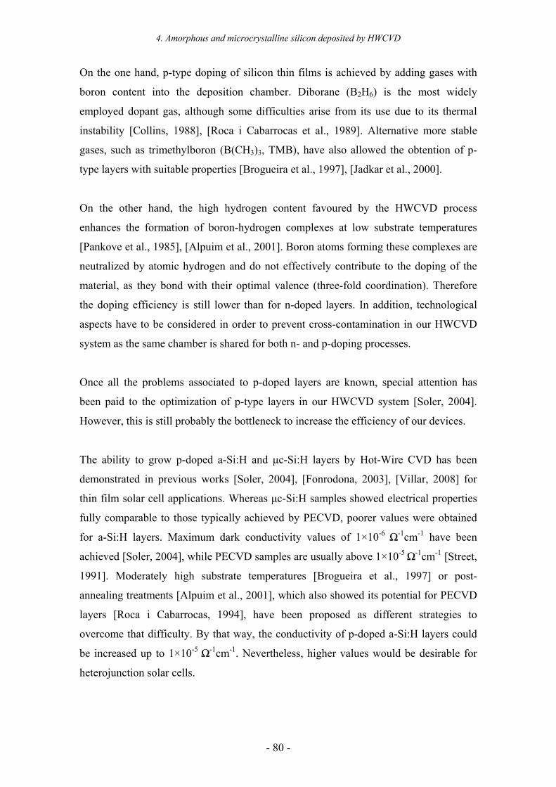
4. Amorphous and microcrystalline silicon deposited by HWCVD
- 80 -
On the one hand, p-type doping of silicon thin films is achieved by adding gases with
boron content into the deposition chamber. Diborane (B2H6) is the most widely
employed dopant gas, although some difficulties arise from its use due to its thermal
instability [Collins, 1988], [Roca i Cabarrocas et al., 1989]. Alternative more stable
gases, such as trimethylboron (B(CH3)3, TMB), have also allowed the obtention of p-
type layers with suitable properties [Brogueira et al., 1997], [Jadkar et al., 2000].
On the other hand, the high hydrogen content favoured by the HWCVD process
enhances the formation of boron-hydrogen complexes at low substrate temperatures
[Pankove et al., 1985], [Alpuim et al., 2001]. Boron atoms forming these complexes are
neutralized by atomic hydrogen and do not effectively contribute to the doping of the
material, as they bond with their optimal valence (three-fold coordination). Therefore
the doping efficiency is still lower than for n-doped layers. In addition, technological
aspects have to be considered in order to prevent cross-contamination in our HWCVD
system as the same chamber is shared for both n- and p-doping processes.
Once all the problems associated to p-doped layers are known, special attention has
been paid to the optimization of p-type layers in our HWCVD system [Soler, 2004].
However, this is still probably the bottleneck to increase the efficiency of our devices.
The ability to grow p-doped a-Si:H and µc-Si:H layers by Hot-Wire CVD has been
demonstrated in previous works [Soler, 2004], [Fonrodona, 2003], [Villar, 2008] for
thin film solar cell applications. Whereas µc-Si:H samples showed electrical properties
fully comparable to those typically achieved by PECVD, poorer values were obtained
for a-Si:H layers. Maximum dark conductivity values of 1×10⁻⁶ Ω-1cm-1 have been
achieved [Soler, 2004], while PECVD samples are usually above 1×10⁻⁵ Ω-1cm-1 [Street,
1991]. Moderately high substrate temperatures [Brogueira et al., 1997] or post-
annealing treatments [Alpuim et al., 2001], which also showed its potential for PECVD
layers [Roca i Cabarrocas, 1994], have been proposed as different strategies to
overcome that difficulty. By that way, the conductivity of p-doped a-Si:H layers could
be increased up to 1×10⁻⁵ Ω-1cm-1. Nevertheless, higher values would be desirable for
heterojunction solar cells.
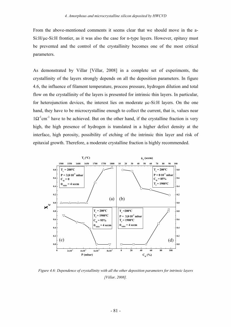
4. Amorphous and microcrystalline silicon deposited by HWCVD
- 81 -
From the above-mentioned comments it seems clear that we should move in the a-
Si:H/µc-Si:H frontier, as it was also the case for n-type layers. However, epitaxy must
be prevented and the control of the crystallinity becomes one of the most critical
parameters.
As demonstrated by Villar [Villar, 2008] in a complete set of experiments, the
crystallinity of the layers strongly depends on all the deposition parameters. In figure
4.6, the influence of filament temperature, process pressure, hydrogen dilution and total
flow on the crystallinity of the layers is presented for intrinsic thin layers. In particular,
for heterojunction devices, the interest lies on moderate µc-Si:H layers. On the one
hand, they have to be microcrystalline enough to collect the current, that is, values near
1Ω-1cm-1 have to be achieved. But on the other hand, if the crystalline fraction is very
high, the high presence of hydrogen is translated in a higher defect density at the
interface, high porosity, possibility of etching of the intrinsic thin layer and risk of
epitaxial growth. Therefore, a moderate crystalline fraction is highly recommended.
1500 1550 1600 1650 1700 1750 1800
0.0
0.2
0.4
0.6
0.8
10 20 30 40 50 60 70 80 90 100
0.0
0.2
0.4
0.6
0.8
0 2x10⁻² 4x10⁻² 6x10⁻² 8x10⁻²
0.0
0.2
0.4
0.6
0.8
0 20 40 60 80 100
0.0
0.2
0.4
0.6
0.8
(c)
(b)
(d)
Tc = 200ºC
P = 3,8·10-2 mbarCH = 0ΦSiH4 = 4 sccm
(a)
Tc =200ºC
P = 3,8·10-2 mbarTf = 1900ºCΦSiH4 = 4 sccm
Tc = 200ºC
P = 8·10-2 mbarCH = 85%Tf = 1900ºC
φT (sccm)
CH (%)P (mbar)
Tc = 200ºCTf = 1900ºCCH = 95%ΦSiH4 = 4 sccm
x c
Tf (ºC)
Figure 4.6: Dependence of crystallinity with all the other deposition parameters for intrinsic layers
[Villar, 2008].
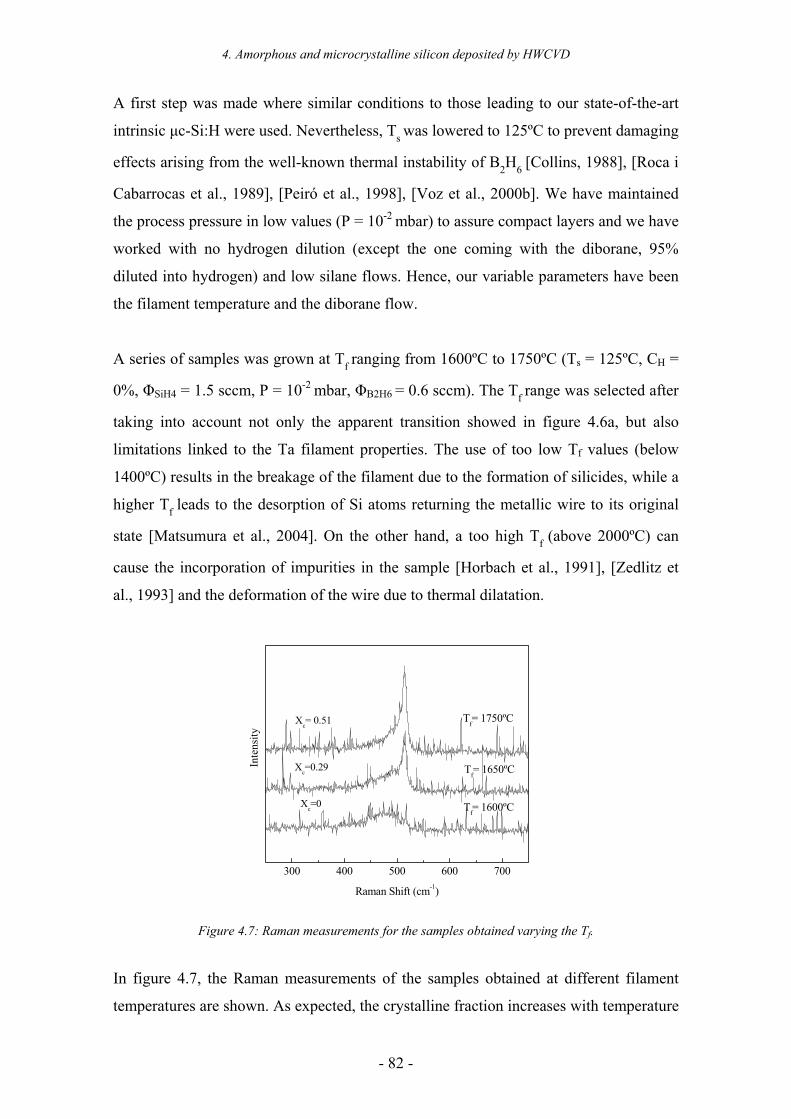
4. Amorphous and microcrystalline silicon deposited by HWCVD
- 82 -
A first step was made where similar conditions to those leading to our state-of-the-art
intrinsic µc-Si:H were used. Nevertheless, Ts was lowered to 125ºC to prevent damaging
effects arising from the well-known thermal instability of B2H6 [Collins, 1988], [Roca i
Cabarrocas et al., 1989], [Peiró et al., 1998], [Voz et al., 2000b]. We have maintained
the process pressure in low values (P = 10-2 mbar) to assure compact layers and we have
worked with no hydrogen dilution (except the one coming with the diborane, 95%
diluted into hydrogen) and low silane flows. Hence, our variable parameters have been
the filament temperature and the diborane flow.
A series of samples was grown at Tf ranging from 1600ºC to 1750ºC (Ts = 125ºC, CH =
0%, ΦSiH4 = 1.5 sccm, P = 10-2 mbar, ΦB2H6 = 0.6 sccm). The Tf range was selected after
taking into account not only the apparent transition showed in figure 4.6a, but also
limitations linked to the Ta filament properties. The use of too low Tf values (below
1400ºC) results in the breakage of the filament due to the formation of silicides, while a
higher Tf leads to the desorption of Si atoms returning the metallic wire to its original
state [Matsumura et al., 2004]. On the other hand, a too high Tf (above 2000ºC) can
cause the incorporation of impurities in the sample [Horbach et al., 1991], [Zedlitz et
al., 1993] and the deformation of the wire due to thermal dilatation.
300 400 500 600 700
Tf= 1600ºC
Tf= 1650ºC
Xc= 0.51
Xc=0.29
Inte
nsity
Raman Shift (cm-1)
Xc=0
Tf= 1750ºC
Figure 4.7: Raman measurements for the samples obtained varying the Tf.
In figure 4.7, the Raman measurements of the samples obtained at different filament
temperatures are shown. As expected, the crystalline fraction increases with temperature
4. Amorphous and microcrystalline silicon deposited by HWCVD
- 83 -
from a totally amorphous structure to Xc higher than 50%. This is also observed in the
conductivity measurements where an improvement from values down to 10-5 to 10-1 Ω-1
cm-1 for the higher Tf sample is seen.
Subsequently, we have also studied p-doped layers with increased dopant concentration.
It is important to remark that two contrary effects are present: the higher hydrogen
dilution due to the increased diborane flow (95% diluted in hydrogen) that promotes
crystalline growth and the amorphisation produced by greater concentrations of
diborane [Voz et al., 2000].
After technological optimization, different p-type materials with an Xc value in the
range of 20-50% and good electrical conductivity have been obtained. It is important to
remark that all the p-type layers studied were quite thick (≈1 µm), while much thinner
layers are used in heterojunction devices. Furthermore, we have to take also into
account that the incubation phase and posterior growth strongly depend on the substrate
used in each case. The above-mentioned experiments were performed on glass while in
heterojunction solar cells the p-layer is grown either on an (i) a-Si:H buffer layer or
directly on the c-Si wafer. Consequently, the main analysis and discussion related to p-
doped layers was done directly on c-Si wafers. These studies are presented in the next
chapter.
5. Precursor fabrication & characterization
- 84 -
Chapter 5: Precursor fabrication
& characterization
“Sembremos la llanura antes de arar la loma”
Pablo Neruda
In this chapter, a further step in the characterization of solar cell precursors is presented.
Optimized a-Si:H films deposited by HWCVD on Corning glass are the starting point,
as it has been discussed in the previous chapter. Then, a-Si:H thin films have been
deposited onto c-Si wafers for the fabrication of heterojunction solar cells. The
characterization of the solar cell precursor determines the influence of the different
substrate in the growing process of a-Si:H films. Besides, a precise determination of the
film thickness is also important since this parameter strongly influences the device
performance.
In this chapter mainly two powerful techniques have been used to characterize solar cell
precursors: the Spectroscopic Ellipsometry and the Quasy-Steady-State
Photoconductance technique (QSSPC). In the case of QSSPC measurements, bifacial
precursors or alternatively back-passivated structures are required (see figure 5.1). For
back passivation usually dielectric hydrogenated a-SiCx films deposited by PECVD
have been used. Since these films allow excellent τeff > 500 µs values (Seff < 25 cm·s-1)
[Ferre et al., 2006], QSSPC data determine the passivation quality of the a-Si:H films
deposited by HWCVD.
5. Precursor fabrication & characterization
- 85 -
In the first part of this chapter, we will focus on the optimization of heterojunction
emitters. As we have basically used p-type wafers, the heterojunction emitter consists in
an n-doped layer and, in some cases, an intrinsic buffer layer. Next, the study of low-
temperature deposited BSF contacts is considered. This low-temperature BSF is formed
by a p-doped layer with again the possibility of inserting a thin intrinsic buffer layer.
Finally, some preliminary studies of the symmetric structures on n-type wafers are
presented.
Figure 5.1: Diagram of the two precursors used in this work: with a back a-SiCx passivating layer
deposited by PECVD (left) and bifacial precursor with the same layer on both sides (right).
5.1 Characterization of HWCVD heterojunction emitters on p-type
wafers
The a-Si:H/c-Si structure has been widely studied for its application in heterojunction
solar cells. The complementary properties of each material can lead to the fabrication of
high efficiency solar cells: a high short-circuit current can be obtained with the c-Si
substrate, while optimized a-Si:H emitters promote high open-circuit voltages. Different
emitter configurations considering also the introduction of an intrinsic buffer and the
effect of pre- and post-treatments will be studied.
5.1.1 Band diagram of the heterojunction emitter
First, the band diagram of the a-Si:H/c-Si heterojunction emitter is analyzed in detail for
a better optimization of the device. As it is shown in figure 5.2, the a-Si:H band gap
(Eg(a-Si:H) ~ 1.8 eV) is larger compared to the c-Si one (Eg(c-Si) = 1.12 eV), while the
electron affinity is higher for c-Si.
c-Si
PECVD a-SiCx
HWCVD a-Si:Hc-Si
HWCVD a-Si:H
HWCVD a-Si:H
5. Precursor fabrication & characterization
- 86 -
(p) c-Si (n) a-Si:H
Ec
Ef
EvEg(a-Si:H)
Eg (c-Si)
ξ c
ξa
∆Ev
∆Ec
Φc
E0
qVbiqΧc
qΧa
qVbic
qVbia
(p) c-Si (n) a-Si:H
Ec
Ef
EvEg(a-Si:H)
Eg (c-Si)
ξ c
ξa
∆Ev
∆Ec
Φc
E0
qVbiqΧc
qΧa
qVbic
qVbia
Figure 5.2 Band diagram for a (n)a-Si:H/(p)c-Si heterojunction emitter.
According to the Anderson’s law [Anderson, 1962], the discontinuity in the conduction
band ∆Ec is defined by:
cac qqE χχ −=∆
where qχa and qχc are the electron affinities of a-Si:H and c-Si, respectively. Then, the
discontinuity in the valence band ∆Ev can be calculated:
cHSicgHSiagv EEEE ∆−−=∆ −− ):():(
and we define the built-in potential qVbi as:
ccaabi qqqV ξχξχ −−+=
where ξa and ξc are the distances between the Fermi level and the nearest band for the
amorphous and crystalline materials. The built-in voltage can be also defined in terms
of the intra-band parameters:
vcaHSiagbi EEqV ∆−−−= − ξξ):( or
ccaSicgbi EEqV ∆+−−= − ξξ)(
Therefore, there are several ways to increase the qVbi value: increase the band gap of the
amorphous material, increase the doping levels of both materials or adjust the band
discontinuities. This last option is also related to the difference in the band gap of the
materials (Eq. 5.2).
5.1
5.3
5.4
5.2
5. Precursor fabrication & characterization
- 87 -
Anyhow, although this ideal approach gives useful information in relative terms for the
devices optimization, the Anderson’s law is not generally accepted for heterojunction
devices due to the strain effects in the bands because of the lattice change [Van der
Walle et al., 1997].
Then, an empirical approach generally accepted by the community considers that the
band discontinuity can be distributed simply as [Damon-Lacoste, 2007]:
)(31
)():( SicgHSiagc EEE −− −=∆ and )(32
)():( SicgHSiagv EEE −− −=∆
So in order to increase the built-in voltage of the emitter higher a-Si:H band gap is
desired.
5.1.2 Limits to the open-circuit voltage
The interest for a higher built-in voltage lies in its direct relation with the open-circuit
voltage of the device. In a very simplified view, the open-circuit voltage is given by:
Voc = BUILT-IN VOLTAGE – RECOMBINATION INFLUENCE 5.6
Thus, the built-in voltage affects positively the Voc value while recombination losses act
as a limiting factor. An analysis by Jensen [Jensen, 2000] of the recombination
mechanisms limiting the final Voc of the device considers three main contributions to
the saturation current density of the diode, j0.
,int0,0,00 jjjj SCRbulk ++=
Since in our case we use FZ wafers with a high diffusion length Leff, the term j0,SCR
related to recombination within the space charge region can be disregarded [Jensen,
2000]. Concerning the bulk saturation current density j0,bulk, it can be calculated as:
effA
ibulk LN
qDnj2
,0 =
Here q denotes the elementary charge, D is the diffusion constant of the minority
carriers, ni is the intrinsic carrier density, and NA is the doping density of the absorber
layer. If we consider a Leff value of 1000 µm and D = 25 cm/s for FZ p-type wafers with
NA = 1016 cm-3, then j0 = 45 fA/cm2. This value would allow a Voc,bulk value up to:
5.5
5.7
5.8
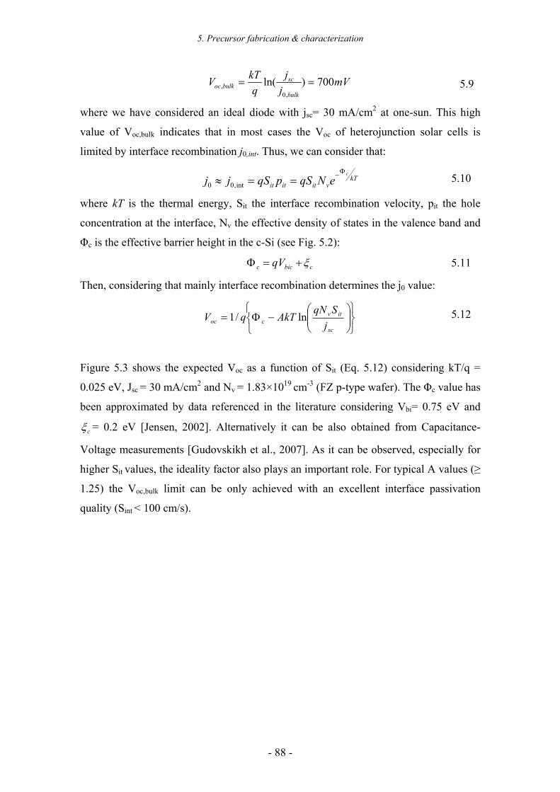
5. Precursor fabrication & characterization
- 88 -
mVjj
qkTV
bulk
scbulkoc 700)ln(
,0, ==
where we have considered an ideal diode with jsc= 30 mA/cm2 at one-sun. This high
value of Voc,bulk indicates that in most cases the Voc of heterojunction solar cells is
limited by interface recombination j0,int. Thus, we can consider that:
kTvititit
c
eNqSpqSjjΦ−
==≈ int,00
where kT is the thermal energy, Sit the interface recombination velocity, pit the hole
concentration at the interface, Nv the effective density of states in the valence band and
Φc is the effective barrier height in the c-Si (see Fig. 5.2):
cbicc qV ξ+=Φ
Then, considering that mainly interface recombination determines the j0 value:
−Φ=
sc
itvcoc j
SqNAkTqV ln/1
Figure 5.3 shows the expected Voc as a function of Sit (Eq. 5.12) considering kT/q =
0.025 eV, Jsc = 30 mA/cm2 and Nv = 1.83×1019 cm-3 (FZ p-type wafer). The Φc value has
been approximated by data referenced in the literature considering Vbi= 0.75 eV and
cξ = 0.2 eV [Jensen, 2002]. Alternatively it can be also obtained from Capacitance-
Voltage measurements [Gudovskikh et al., 2007]. As it can be observed, especially for
higher Sit values, the ideality factor also plays an important role. For typical A values (≥
1.25) the Voc,bulk limit can be only achieved with an excellent interface passivation
quality (Sint < 100 cm/s).
5.10
5.11
5.12
5.9
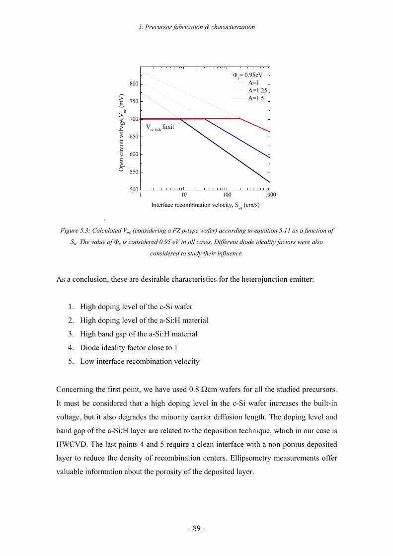
5. Precursor fabrication & characterization
- 89 -
.
1 10 100 1000500
550
600
650
700
750
800
Ope
n-ci
rcui
t vol
tage
,Voc
(mV
)
Interface recombination velocity, Sint (cm/s)
A=1 A=1.25 A=1.5
Φc= 0.95eV
Voc,bulk limit
Figure 5.3: Calculated Voc (considering a FZ p-type wafer) according to equation 5.11 as a function of
Sit. The value of Φc is considered 0.95 eV in all cases. Different diode ideality factors were also
considered to study their influence.
As a conclusion, these are desirable characteristics for the heterojunction emitter:
1. High doping level of the c-Si wafer
2. High doping level of the a-Si:H material
3. High band gap of the a-Si:H material
4. Diode ideality factor close to 1
5. Low interface recombination velocity
Concerning the first point, we have used 0.8 Ωcm wafers for all the studied precursors.
It must be considered that a high doping level in the c-Si wafer increases the built-in
voltage, but it also degrades the minority carrier diffusion length. The doping level and
band gap of the a-Si:H layer are related to the deposition technique, which in our case is
HWCVD. The last points 4 and 5 require a clean interface with a non-porous deposited
layer to reduce the density of recombination centers. Ellipsometry measurements offer
valuable information about the porosity of the deposited layer.
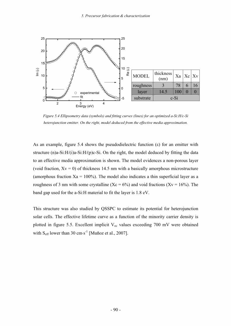
5. Precursor fabrication & characterization
- 90 -
2 3 40
5
10
15
20
25
-5
0
5
10
15
20
25
experimental fit
Im
(ε)
Energy (eV)
Re
(ε)
Figure 5.4 Ellipsometry data (symbols) and fitting curves (lines) for an optimized a-Si:H/c-Si
heterojunction emitter. On the right, model deduced from the effective media approximation.
As an example, figure 5.4 shows the pseudodielectric function (ε) for an emitter with
structure (n)a-Si:H/(i)a-Si:H/(p)c-Si. On the right, the model deduced by fitting the data
to an effective media approximation is shown. The model evidences a non-porous layer
(void fraction, Xv = 0) of thickness 14.5 nm with a basically amorphous microstructure
(amorphous fraction Xa = 100%). The model also indicates a thin superficial layer as a
roughness of 3 nm with some crystalline (Xc = 6%) and void fractions (Xv = 16%). The
band gap used for the a-Si:H material to fit the layer is 1.8 eV.
This structure was also studied by QSSPC to estimate its potential for heterojunction
solar cells. The effective lifetime curve as a function of the minority carrier density is
plotted in figure 5.5. Excellent implicit Voc values exceeding 700 mV were obtained
with Seff lower than 30 cm⋅s-1 [Muñoz et al., 2007].
MODEL thickness (nm) Xa Xc Xv
roughness 3 78 6 16layer 14.5 100 0 0
substrate c-Si
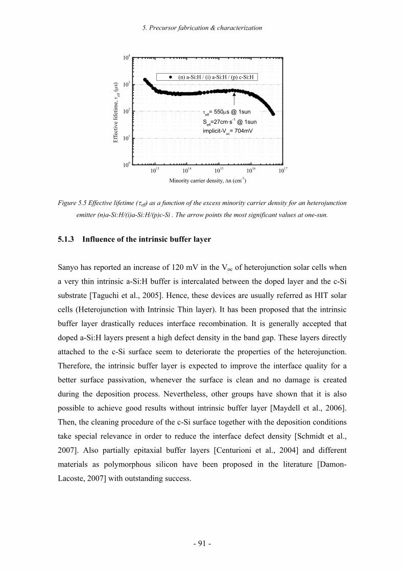
5. Precursor fabrication & characterization
- 91 -
1013 1014 1015 1016 1017100
101
102
103
104
Effe
ctiv
e lif
etim
e, τ ef
f (µs)
Minority carrier density, ∆n (cm-3)
(n) a-Si:H / (i) a-Si:H / (p) c-Si:H
τeff= 550µs @ 1sun
Seff=27cm·s-1 @ 1sunimplicit-Voc= 704mV
Figure 5.5 Effective lifetime (τeff) as a function of the excess minority carrier density for an heterojunction
emitter (n)a-Si:H/(i)a-Si:H/(p)c-Si . The arrow points the most significant values at one-sun.
5.1.3 Influence of the intrinsic buffer layer
Sanyo has reported an increase of 120 mV in the Voc of heterojunction solar cells when
a very thin intrinsic a-Si:H buffer is intercalated between the doped layer and the c-Si
substrate [Taguchi et al., 2005]. Hence, these devices are usually referred as HIT solar
cells (Heterojunction with Intrinsic Thin layer). It has been proposed that the intrinsic
buffer layer drastically reduces interface recombination. It is generally accepted that
doped a-Si:H layers present a high defect density in the band gap. These layers directly
attached to the c-Si surface seem to deteriorate the properties of the heterojunction.
Therefore, the intrinsic buffer layer is expected to improve the interface quality for a
better surface passivation, whenever the surface is clean and no damage is created
during the deposition process. Nevertheless, other groups have shown that it is also
possible to achieve good results without intrinsic buffer layer [Maydell et al., 2006].
Then, the cleaning procedure of the c-Si surface together with the deposition conditions
take special relevance in order to reduce the interface defect density [Schmidt et al.,
2007]. Also partially epitaxial buffer layers [Centurioni et al., 2004] and different
materials as polymorphous silicon have been proposed in the literature [Damon-
Lacoste, 2007] with outstanding success.
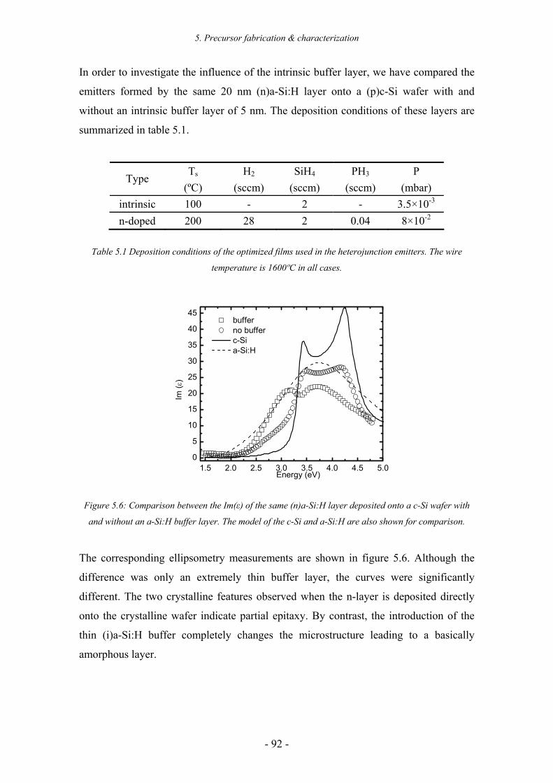
5. Precursor fabrication & characterization
- 92 -
In order to investigate the influence of the intrinsic buffer layer, we have compared the
emitters formed by the same 20 nm (n)a-Si:H layer onto a (p)c-Si wafer with and
without an intrinsic buffer layer of 5 nm. The deposition conditions of these layers are
summarized in table 5.1.
Ts H2 SiH4 PH3 P Type
(ºC) (sccm) (sccm) (sccm) (mbar) intrinsic 100 - 2 - 3.5×10⁻³ n-doped 200 28 2 0.04 8×10⁻²
Table 5.1 Deposition conditions of the optimized films used in the heterojunction emitters. The wire
temperature is 1600ºC in all cases.
1.5 2.0 2.5 3.0 3.5 4.0 4.5 5.00
5
10
15
20
25
30
35
40
45
buffer no buffer c-Si a-Si:H
Im (ε
)
Energy (eV)
Figure 5.6: Comparison between the Im(ε) of the same (n)a-Si:H layer deposited onto a c-Si wafer with
and without an a-Si:H buffer layer. The model of the c-Si and a-Si:H are also shown for comparison.
The corresponding ellipsometry measurements are shown in figure 5.6. Although the
difference was only an extremely thin buffer layer, the curves were significantly
different. The two crystalline features observed when the n-layer is deposited directly
onto the crystalline wafer indicate partial epitaxy. By contrast, the introduction of the
thin (i)a-Si:H buffer completely changes the microstructure leading to a basically
amorphous layer.
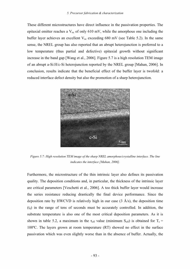
5. Precursor fabrication & characterization
- 93 -
These different microstructures have direct influence in the passivation properties. The
epitaxial emitter reaches a Voc of only 610 mV, while the amorphous one including the
buffer layer achieves an excellent Voc exceeding 680 mV (see Table 5.2). In the same
sense, the NREL group has also reported that an abrupt heterojunction is preferred to a
low temperature (thus partial and defective) epitaxial growth without significant
increase in the band gap [Wang et al., 2006]. Figure 5.7 is a high resolution TEM image
of an abrupt a-Si:H/c-Si heterojunction reported by the NREL group [Mahan, 2006]. In
conclusion, results indicate that the beneficial effect of the buffer layer is twofold: a
reduced interface defect density but also the promotion of a sharp heterojunction.
Figure 5.7: High resolution TEM image of the sharp NREL amorphous/crystalline interface. The line
indicates the interface [Mahan, 2006].
Furthermore, the microstructure of the thin intrinsic layer also defines its passivation
quality. The deposition conditions and, in particular, the thickness of the intrinsic layer
are critical parameters [Veschetti et al., 2006]. A too thick buffer layer would increase
the series resistance reducing drastically the final device performance. Since the
deposition rate by HWCVD is relatively high in our case (3 Å/s), the deposition time
(td) in the range of tens of seconds must be accurately controlled. In addition, the
substrate temperature is also one of the most critical deposition parameters. As it is
shown in table 5.2, a maximum in the τeff value (minimum Seff) is obtained for Ts =
100ºC. The layers grown at room temperature (RT) showed no effect in the surface
passivation which was even slightly worse than in the absence of buffer. Actually, the
5. Precursor fabrication & characterization
- 94 -
layer grown at room temperature evidenced a very high porosity at the interface. These
results are similar at those obtained by [Wang et al., 2006].
Ts SiH4 P td Thickness implicit-Voc τeff Intrinsic layer (ºC) (sccm) (mbar) (s) (nm) (V) (µs)
- - - - - - 600 17 IRT RT 2 3.5×10⁻³ 15 5 596 11 I100 100 2 3.5×10⁻³ 15 5 670 214 I200 200 2 3.5×10⁻³ 15 5 638 66 Ithin 100 2 3.5×10⁻³ 10 3 621 33 Ithick 100 2 3.5×10⁻³ 30 10 680 273
Table 5.2: Different intrinsic a-Si:H thin layers used in the heterojunction emitter and passivation quality
measured by QSSPC. The 20 nm n-doped layer was the same in all cases with the deposition parameters
in table 5.1.
In order to study the microstructure of the intrinsic a-Si:H material, a single 5 nm a-Si:H
layer was deposited on c-Si without subsequent n-doped emitter. Figure 5.8 shows the
ellipsometry data fitted following the Tauc-Lorenz model. The c-Si surface was cleaned
and dipped into HF in order to remove the native oxide and assure good interface
properties. In this particular case, the cleaning process was very critical due to the
strong influence of the interface in the fit. As it is shown in the inset of figure 5.8, the
band of the a-Si:H material deposited by HWCVD is significantly lower than for the
standard a-Si:H model. This result can be related to the porosity of the layer which leads
to a lower compactness (A value) in the model. Other groups have also referenced a
higher porosity in HWCVD a-Si:H films compared to other deposition techniques [Liu
et al., 2002]. The rest of parameters are quite similar to the standard material and
similar properties are expected. Actually, the ellipsometry curve could be also fitted
quite well by the standard a-Si:H material if a void fraction of 30% is considered.
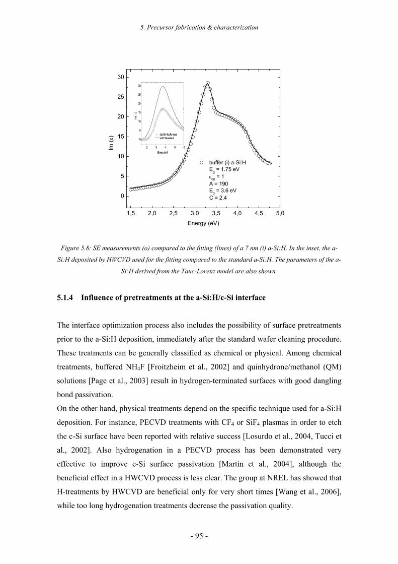
5. Precursor fabrication & characterization
- 95 -
1,5 2,0 2,5 3,0 3,5 4,0 4,5 5,0
0
5
10
15
20
25
30
2 3 4 5 6
0
5
10
15
20
25
30
Im (
ε)
Energy (eV)
(i)a-Si:H buffer layer a-Si:H standard
buffer (i) a-Si:H Eg = 1.75 eV ε00 = 1 A = 190 E0 = 3.6 eV C = 2.4
Im (ε
)
Energy (eV)
Figure 5.8: SE measurements (o) compared to the fitting (lines) of a 7 nm (i) a-Si:H. In the inset, the a-
Si:H deposited by HWCVD used for the fitting compared to the standard a-Si:H. The parameters of the a-
Si:H derived from the Tauc-Lorenz model are also shown.
5.1.4 Influence of pretreatments at the a-Si:H/c-Si interface
The interface optimization process also includes the possibility of surface pretreatments
prior to the a-Si:H deposition, immediately after the standard wafer cleaning procedure.
These treatments can be generally classified as chemical or physical. Among chemical
treatments, buffered NH4F [Froitzheim et al., 2002] and quinhydrone/methanol (QM)
solutions [Page et al., 2003] result in hydrogen-terminated surfaces with good dangling
bond passivation.
On the other hand, physical treatments depend on the specific technique used for a-Si:H
deposition. For instance, PECVD treatments with CF4 or SiF4 plasmas in order to etch
the c-Si surface have been reported with relative success [Losurdo et al., 2004, Tucci et
al., 2002]. Also hydrogenation in a PECVD process has been demonstrated very
effective to improve c-Si surface passivation [Martin et al., 2004], although the
beneficial effect in a HWCVD process is less clear. The group at NREL has showed that
H-treatments by HWCVD are beneficial only for very short times [Wang et al., 2006],
while too long hydrogenation treatments decrease the passivation quality.
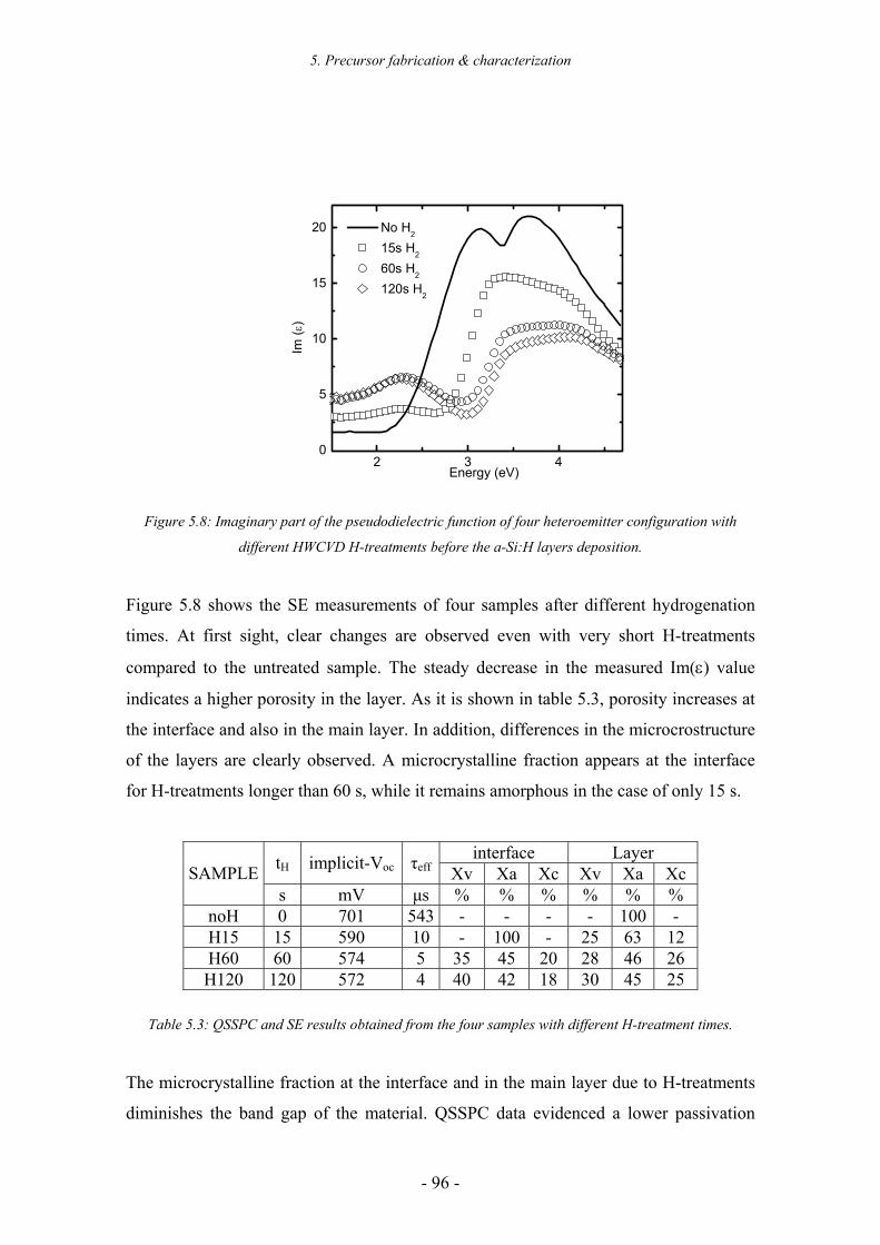
5. Precursor fabrication & characterization
- 96 -
2 3 40
5
10
15
20 No H2
15s H2
60s H2
120s H2
Im (ε
)
Energy (eV)
Figure 5.8: Imaginary part of the pseudodielectric function of four heteroemitter configuration with
different HWCVD H-treatments before the a-Si:H layers deposition.
Figure 5.8 shows the SE measurements of four samples after different hydrogenation
times. At first sight, clear changes are observed even with very short H-treatments
compared to the untreated sample. The steady decrease in the measured Im(ε) value
indicates a higher porosity in the layer. As it is shown in table 5.3, porosity increases at
the interface and also in the main layer. In addition, differences in the microcrostructure
of the layers are clearly observed. A microcrystalline fraction appears at the interface
for H-treatments longer than 60 s, while it remains amorphous in the case of only 15 s.
interface Layer tH implicit-Voc τeff Xv Xa Xc Xv Xa Xc SAMPLEs mV µs % % % % % %
noH 0 701 543 - - - - 100 - H15 15 590 10 - 100 - 25 63 12 H60 60 574 5 35 45 20 28 46 26 H120 120 572 4 40 42 18 30 45 25
Table 5.3: QSSPC and SE results obtained from the four samples with different H-treatment times.
The microcrystalline fraction at the interface and in the main layer due to H-treatments
diminishes the band gap of the material. QSSPC data evidenced a lower passivation
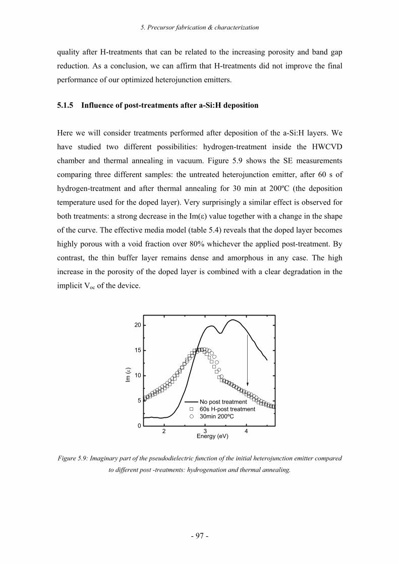
5. Precursor fabrication & characterization
- 97 -
quality after H-treatments that can be related to the increasing porosity and band gap
reduction. As a conclusion, we can affirm that H-treatments did not improve the final
performance of our optimized heterojunction emitters.
5.1.5 Influence of post-treatments after a-Si:H deposition
Here we will consider treatments performed after deposition of the a-Si:H layers. We
have studied two different possibilities: hydrogen-treatment inside the HWCVD
chamber and thermal annealing in vacuum. Figure 5.9 shows the SE measurements
comparing three different samples: the untreated heterojunction emitter, after 60 s of
hydrogen-treatment and after thermal annealing for 30 min at 200ºC (the deposition
temperature used for the doped layer). Very surprisingly a similar effect is observed for
both treatments: a strong decrease in the Im(ε) value together with a change in the shape
of the curve. The effective media model (table 5.4) reveals that the doped layer becomes
highly porous with a void fraction over 80% whichever the applied post-treatment. By
contrast, the thin buffer layer remains dense and amorphous in any case. The high
increase in the porosity of the doped layer is combined with a clear degradation in the
implicit Voc of the device.
2 3 40
5
10
15
20
No post treatment 60s H-post treatment 30min 200ºC
Im (ε
)
Energy (eV)
Figure 5.9: Imaginary part of the pseudodielectric function of the initial heterojunction emitter compared
to different post -treatments: hydrogenation and thermal annealing.
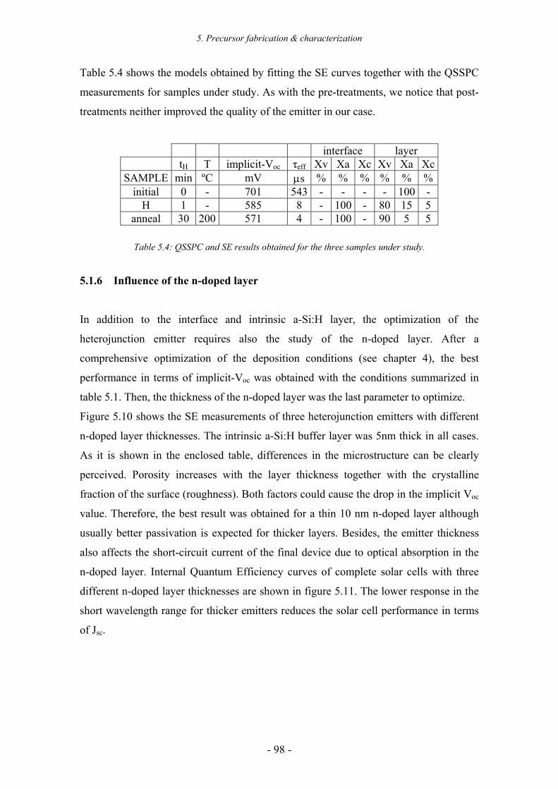
5. Precursor fabrication & characterization
- 98 -
Table 5.4 shows the models obtained by fitting the SE curves together with the QSSPC
measurements for samples under study. As with the pre-treatments, we notice that post-
treatments neither improved the quality of the emitter in our case.
interface layer tH T implicit-Voc τeff Xv Xa Xc Xv Xa Xc
SAMPLE min ºC mV µs % % % % % % initial 0 - 701 543 - - - - 100 -
H 1 - 585 8 - 100 - 80 15 5 anneal 30 200 571 4 - 100 - 90 5 5
Table 5.4: QSSPC and SE results obtained for the three samples under study.
5.1.6 Influence of the n-doped layer
In addition to the interface and intrinsic a-Si:H layer, the optimization of the
heterojunction emitter requires also the study of the n-doped layer. After a
comprehensive optimization of the deposition conditions (see chapter 4), the best
performance in terms of implicit-Voc was obtained with the conditions summarized in
table 5.1. Then, the thickness of the n-doped layer was the last parameter to optimize.
Figure 5.10 shows the SE measurements of three heterojunction emitters with different
n-doped layer thicknesses. The intrinsic a-Si:H buffer layer was 5nm thick in all cases.
As it is shown in the enclosed table, differences in the microstructure can be clearly
perceived. Porosity increases with the layer thickness together with the crystalline
fraction of the surface (roughness). Both factors could cause the drop in the implicit Voc
value. Therefore, the best result was obtained for a thin 10 nm n-doped layer although
usually better passivation is expected for thicker layers. Besides, the emitter thickness
also affects the short-circuit current of the final device due to optical absorption in the
n-doped layer. Internal Quantum Efficiency curves of complete solar cells with three
different n-doped layer thicknesses are shown in figure 5.11. The lower response in the
short wavelength range for thicker emitters reduces the solar cell performance in terms
of Jsc.
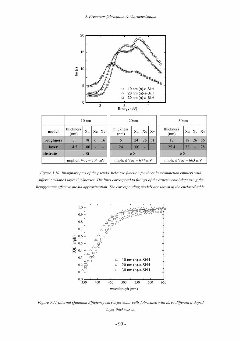
5. Precursor fabrication & characterization
- 99 -
2 3 40
5
10
15
20
10 nm (n)-a-Si:H 20 nm (n)-a-Si:H 30 nm (n)-a-Si:H
Im (ε
)
Energy (eV)
10 nm 20nm 30nm
model thickness (nm) Xa Xc Xv thickness
(nm) Xa Xc Xv thickness (nm) Xa Xc Xv
roughness 3 78 6 16 5 24 25 51 12 18 26 56
layer 14.5 100 - - 24 100 - 25.4 72 - 28
substrate c-Si c-Si c-Si
implicit Voc = 704 mV implicit Voc = 677 mV implicit Voc = 663 mV
Figure 5.10: Imaginary part of the pseudo dielectric function for three heterojunction emitters with
different n-doped layer thicknesses. The lines correspond to fittings of the experimental data using the
Bruggemann effective media approximation. The corresponding models are shown in the enclosed table.
350 400 450 500 550 600 6500.0
0.1
0.2
0.3
0.4
0.5
0.6
0.7
0.8
0.9
1.0
IQE
(e/p
h)
wavelength (nm)
10 nm (n)-a-Si:H 20 nm (n)-a-Si:H 30 nm (n)-a-Si:H
Figure 5.11 Internal Quantum Efficiency curves for solar cells fabricated with three different n-doped
layer thicknesses.
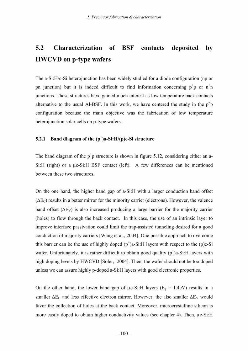
5. Precursor fabrication & characterization
- 100 -
5.2 Characterization of BSF contacts deposited by
HWCVD on p-type wafers
The a-Si:H/c-Si heterojunction has been widely studied for a diode configuration (np or
pn junction) but it is indeed difficult to find information concerning p+p or n+n
junctions. These structures have gained much interest as low temperature back contacts
alternative to the usual Al-BSF. In this work, we have centered the study in the p+p
configuration because the main objective was the fabrication of low temperature
heterojunction solar cells on p-type wafers.
5.2.1 Band diagram of the (p+)a-Si:H/(p)c-Si structure
The band diagram of the p+p structure is shown in figure 5.12, considering either an a-
Si:H (right) or a µc-Si:H BSF contact (left). A few differences can be mentioned
between these two structures.
On the one hand, the higher band gap of a-Si:H with a larger conduction band offset
(∆EC) results in a better mirror for the minority carrier (electrons). However, the valence
band offset (∆EV) is also increased producing a large barrier for the majority carrier
(holes) to flow through the back contact. In this case, the use of an intrinsic layer to
improve interface passivation could limit the trap-assisted tunneling desired for a good
conduction of majority carriers [Wang et al., 2004]. One possible approach to overcome
this barrier can be the use of highly doped (p+)a-Si:H layers with respect to the (p)c-Si
wafer. Unfortunately, it is rather difficult to obtain good quality (p+)a-Si:H layers with
high doping levels by HWCVD [Soler, 2004]. Then, the wafer should not be too doped
unless we can assure highly p-doped a-Si:H layers with good electronic properties.
On the other hand, the lower band gap of µc-Si:H layers (Eg ≈ 1.4eV) results in a
smaller ∆EC and less effective electron mirror. However, the also smaller ∆EV would
favor the collection of holes at the back contact. Moreover, microcrystalline silicon is
more easily doped to obtain higher conductivity values (see chapter 4). Then, µc-Si:H
5. Precursor fabrication & characterization
- 101 -
layers deserve special consideration for the optimization of low-temperature BSF
contacts. Furthermore, interface passivation must be also taken into account whichever
structure is used.
Eg (c-Si)
Eg(a-Si:H)
qVbi
qΧa
qΧc
ξaξ c
(p) c-Si (p+) a-Si:H
Eg (c-Si)
Eg(µc-Si:H)
qVbi
qΧµc
qΧc
ξµc
ξ c
(p) c-Si (p+) µc-Si:H
Figure 5.12: Band diagram of a (p+)a-Si:H/(p)c-Si (right) and (p+)µc-Si:H/(p)c-Si heterojunction (left).
The desired properties for the back contact can be summarized:
1. High doping level of the a-Si:H/µc-Si:H material
2. High doping level of the c-Si wafer (limited by the success in 1)
3. High band gap of the a-Si:H/µc-Si:H material
4. Low interface recombination velocity
In addition, these properties have to be compatible with technological aspects related to
the deposition technique. In this work, the study of low temperature BSF contacts will
be centered on the deposition of good quality p-doped layers by HWCVD. In order to
achieve the desired microstructure and passivation properties we have comprehensively
studied the influence of the deposition parameters. The effect of a thin intrinsic buffer
layer is also carefully analyzed. However, it is important to remark that good precursors
do not assure good BSF contacts, since carrier collection is actually not considered. The
study of complete solar cells is part of the next chapter.
5. Precursor fabrication & characterization
- 102 -
5.2.2 Optimization of the p-doped layer
As for the heterojunction emitter, we have considered the configuration with and
without an intrinsic buffer layer. Firstly, we have studied the properties of p-doped
layers deposited on c-Si substrates. Considering that it is much more difficult to achieve
good electronic properties when doping with boron, the a-Si:H layers were extensively
studied varying the different deposition parameters.
a) Influence of the diborane flow and filament temperature
One of the more critical parameters affecting the microstructure of the material is the
diborane (B2H6) flow. On the one hand, it has been reported that diborane promotes
amorphization of the layers [Voz et al., 2000]. The structural change due to boron
incorporation is also accompanied by a change in the hydrogen bonding environment. It
is also well known that the doping efficiency of boron in a-Si:H is quite low [Winer et
al., 1990]. The doping efficiency is about 10% at low boron concentrations and falls off
to only a fraction of percent as the boron concentration rises. Such a low doping
efficiency is attributed to the belief that most boron atoms are incorporated into
threefold coordinated sites where boron is inert or non-doping. This is in marked
contrast to the situation for c-Si where all the incorporated boron atoms substitute for
silicon atoms obtaining a virtually 100% doping efficiency. In addition, p-doping of a-
Si:H layers is considerably less effective because of the filling of band tail and defect
states.
On the other hand, the use of p+p junctions for the back contact requires a low density of
states at the interface, as well as an effective field-effect passivation. The band bending
at the silicon surface caused by the electric field reduces the density of one carrier type
at the interface (holes in this case), minimizing the recombination velocity. In such
high-low junctions field effect passivation is achieved if we are able to deposit heavily
p-doped a-Si:H layers, otherwise band bending would play a negative role in both
carrier collection and interface passivation.
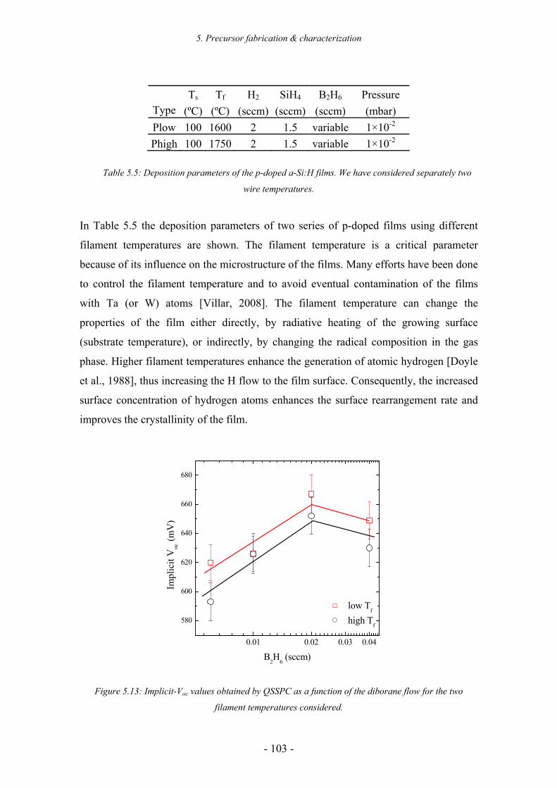
5. Precursor fabrication & characterization
- 103 -
Ts Tf H2 SiH4 B2H6 Pressure Type (ºC) (ºC) (sccm) (sccm) (sccm) (mbar) Plow 100 1600 2 1.5 variable 1×10⁻² Phigh 100 1750 2 1.5 variable 1×10⁻²
Table 5.5: Deposition parameters of the p-doped a-Si:H films. We have considered separately two
wire temperatures.
In Table 5.5 the deposition parameters of two series of p-doped films using different
filament temperatures are shown. The filament temperature is a critical parameter
because of its influence on the microstructure of the films. Many efforts have been done
to control the filament temperature and to avoid eventual contamination of the films
with Ta (or W) atoms [Villar, 2008]. The filament temperature can change the
properties of the film either directly, by radiative heating of the growing surface
(substrate temperature), or indirectly, by changing the radical composition in the gas
phase. Higher filament temperatures enhance the generation of atomic hydrogen [Doyle
et al., 1988], thus increasing the H flow to the film surface. Consequently, the increased
surface concentration of hydrogen atoms enhances the surface rearrangement rate and
improves the crystallinity of the film.
0.01 0.02 0.03 0.04
580
600
620
640
660
680
low Tf
high Tf
Impl
icit
Voc
(mV
)
B2H6 (sccm)
Figure 5.13: Implicit-Voc values obtained by QSSPC as a function of the diborane flow for the two
filament temperatures considered.
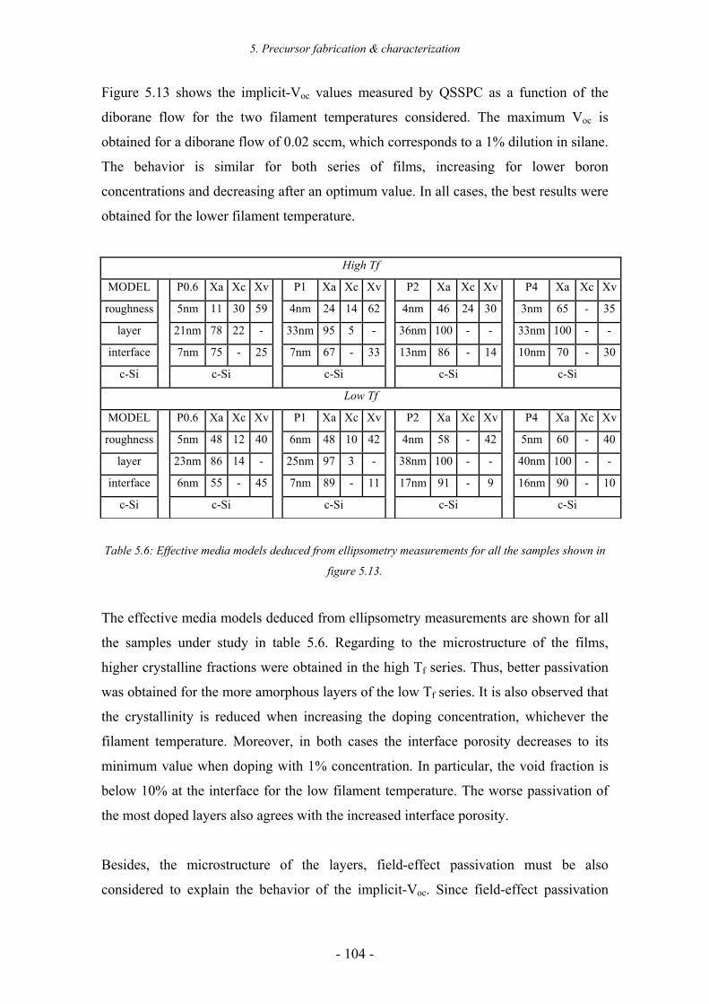
5. Precursor fabrication & characterization
- 104 -
Figure 5.13 shows the implicit-Voc values measured by QSSPC as a function of the
diborane flow for the two filament temperatures considered. The maximum Voc is
obtained for a diborane flow of 0.02 sccm, which corresponds to a 1% dilution in silane.
The behavior is similar for both series of films, increasing for lower boron
concentrations and decreasing after an optimum value. In all cases, the best results were
obtained for the lower filament temperature.
High Tf
MODEL P0.6 Xa Xc Xv P1 Xa Xc Xv P2 Xa Xc Xv P4 Xa Xc Xv
roughness 5nm 11 30 59 4nm 24 14 62 4nm 46 24 30 3nm 65 - 35
layer 21nm 78 22 - 33nm 95 5 - 36nm 100 - - 33nm 100 - -
interface 7nm 75 - 25 7nm 67 - 33 13nm 86 - 14 10nm 70 - 30
c-Si c-Si c-Si c-Si c-Si
Low Tf
MODEL P0.6 Xa Xc Xv P1 Xa Xc Xv P2 Xa Xc Xv P4 Xa Xc Xv
roughness 5nm 48 12 40 6nm 48 10 42 4nm 58 - 42 5nm 60 - 40
layer 23nm 86 14 - 25nm 97 3 - 38nm 100 - - 40nm 100 - -
interface 6nm 55 - 45 7nm 89 - 11 17nm 91 - 9 16nm 90 - 10
c-Si c-Si c-Si c-Si c-Si
Table 5.6: Effective media models deduced from ellipsometry measurements for all the samples shown in
figure 5.13.
The effective media models deduced from ellipsometry measurements are shown for all
the samples under study in table 5.6. Regarding to the microstructure of the films,
higher crystalline fractions were obtained in the high Tf series. Thus, better passivation
was obtained for the more amorphous layers of the low Tf series. It is also observed that
the crystallinity is reduced when increasing the doping concentration, whichever the
filament temperature. Moreover, in both cases the interface porosity decreases to its
minimum value when doping with 1% concentration. In particular, the void fraction is
below 10% at the interface for the low filament temperature. The worse passivation of
the most doped layers also agrees with the increased interface porosity.
Besides, the microstructure of the layers, field-effect passivation must be also
considered to explain the behavior of the implicit-Voc. Since field-effect passivation
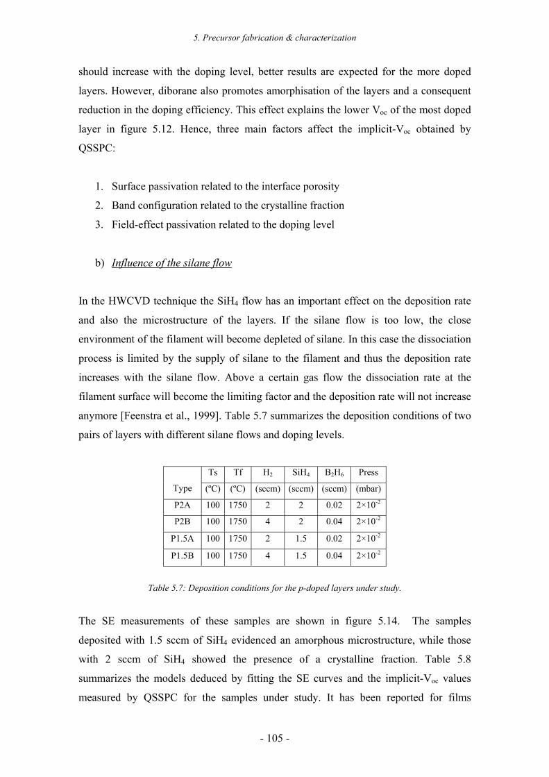
5. Precursor fabrication & characterization
- 105 -
should increase with the doping level, better results are expected for the more doped
layers. However, diborane also promotes amorphisation of the layers and a consequent
reduction in the doping efficiency. This effect explains the lower Voc of the most doped
layer in figure 5.12. Hence, three main factors affect the implicit-Voc obtained by
QSSPC:
1. Surface passivation related to the interface porosity
2. Band configuration related to the crystalline fraction
3. Field-effect passivation related to the doping level
b) Influence of the silane flow
In the HWCVD technique the SiH4 flow has an important effect on the deposition rate
and also the microstructure of the layers. If the silane flow is too low, the close
environment of the filament will become depleted of silane. In this case the dissociation
process is limited by the supply of silane to the filament and thus the deposition rate
increases with the silane flow. Above a certain gas flow the dissociation rate at the
filament surface will become the limiting factor and the deposition rate will not increase
anymore [Feenstra et al., 1999]. Table 5.7 summarizes the deposition conditions of two
pairs of layers with different silane flows and doping levels.
Ts Tf H2 SiH4 B2H6 Press
Type (ºC) (ºC) (sccm) (sccm) (sccm) (mbar)
P2A 100 1750 2 2 0.02 2×10⁻²
P2B 100 1750 4 2 0.04 2×10⁻²
P1.5A 100 1750 2 1.5 0.02 2×10⁻²
P1.5B 100 1750 4 1.5 0.04 2×10⁻²
Table 5.7: Deposition conditions for the p-doped layers under study.
The SE measurements of these samples are shown in figure 5.14. The samples
deposited with 1.5 sccm of SiH4 evidenced an amorphous microstructure, while those
with 2 sccm of SiH4 showed the presence of a crystalline fraction. Table 5.8
summarizes the models deduced by fitting the SE curves and the implicit-Voc values
measured by QSSPC for the samples under study. It has been reported for films
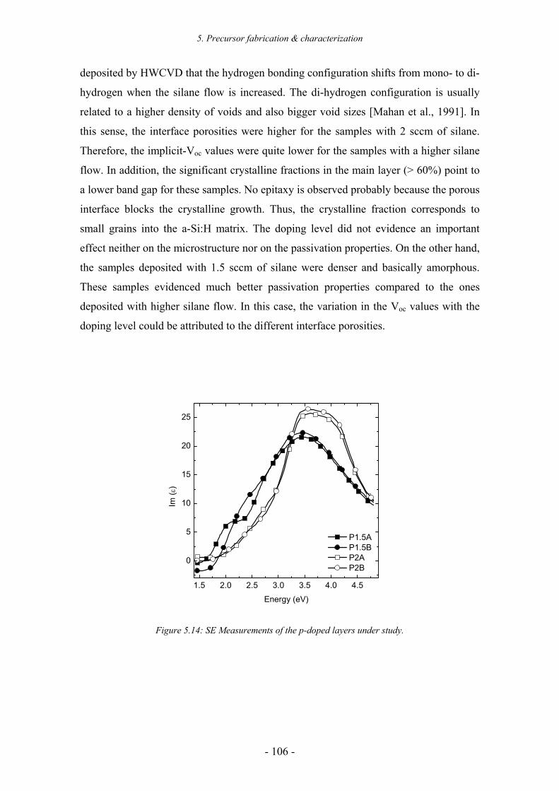
5. Precursor fabrication & characterization
- 106 -
deposited by HWCVD that the hydrogen bonding configuration shifts from mono- to di-
hydrogen when the silane flow is increased. The di-hydrogen configuration is usually
related to a higher density of voids and also bigger void sizes [Mahan et al., 1991]. In
this sense, the interface porosities were higher for the samples with 2 sccm of silane.
Therefore, the implicit-Voc values were quite lower for the samples with a higher silane
flow. In addition, the significant crystalline fractions in the main layer (> 60%) point to
a lower band gap for these samples. No epitaxy is observed probably because the porous
interface blocks the crystalline growth. Thus, the crystalline fraction corresponds to
small grains into the a-Si:H matrix. The doping level did not evidence an important
effect neither on the microstructure nor on the passivation properties. On the other hand,
the samples deposited with 1.5 sccm of silane were denser and basically amorphous.
These samples evidenced much better passivation properties compared to the ones
deposited with higher silane flow. In this case, the variation in the Voc values with the
doping level could be attributed to the different interface porosities.
1.5 2.0 2.5 3.0 3.5 4.0 4.5
0
5
10
15
20
25
Im (ε
)
Energy (eV)
P1.5A P1.5B P2A P2B
Figure 5.14: SE Measurements of the p-doped layers under study.
5. Precursor fabrication & characterization
- 107 -
MODEL P1.5A Xa Xc Xv P1.5B Xa Xc Xv P2A Xa Xc Xv P2A Xa Xc Xv
roughness 4nm 46 24 30 3nm 65 - 35 4nm 25 48 26 3nm 32 43 25
layer 36nm 100 - - 33nm 100 - - 31nm 35 65 - 36nm 34 66 -
interface 13nm 86 - 14 10nm 70 - 30 3nm 65 - 35 4nm 60 - 40
SUBSTRATE c-Si c-Si c-Si c-Si
implicit-Voc 667 mV 649 mV 615 mV 612 mV
Table 5.8: Fittings from the ellipsometry measurements for all the samples plotted in 5.14.
c) Influence of H2 dilution
The microcrystalline films previously studied showed only fair passivation properties
with implicit-Voc values only slightly over 610 mV. Although amorphous layers
allowed much better results, the carrier collection in complete solar cells has to be
confirmed (next chapter). Therefore, in this section we study different deposition
conditions in order to obtain highly conductive microcrystalline p-doped layers with
better passivation quality. Now, the H-dilution is considered since it is well known that
this parameter plays an important role in the microstructure of the film [Niikura et al.,
2000]. Table 5.9 shows the deposition conditions of a film grown with a high hydrogen
dilution.
Ts Tf H2 SiH4 B2H6 Press
Type (ºC) (ºC) (sccm) (sccm) (sccm) (mbar)
PH 100 1750 100 4 0.02 3×10⁻²
Table 5.9: Deposition conditions for a film grown with a high H-dilution.
In this case, the SE measurement of the layer evidenced a clearly crystalline
microstructure (figure 5.15). In particular, the imaginary part of the pseudo dielectric
function resembles the model of a big grain µc-Si:H material. The effective media
model deduced by fitting the SE curve is shown in table 5.10.
The lower Im<ε> value of the sample PH compared to the models can be attributed to
the high void fraction on the surface (roughness), which strongly diminishes the high
energy peak. Since the crystalline fraction is actually formed by a mixture of small and
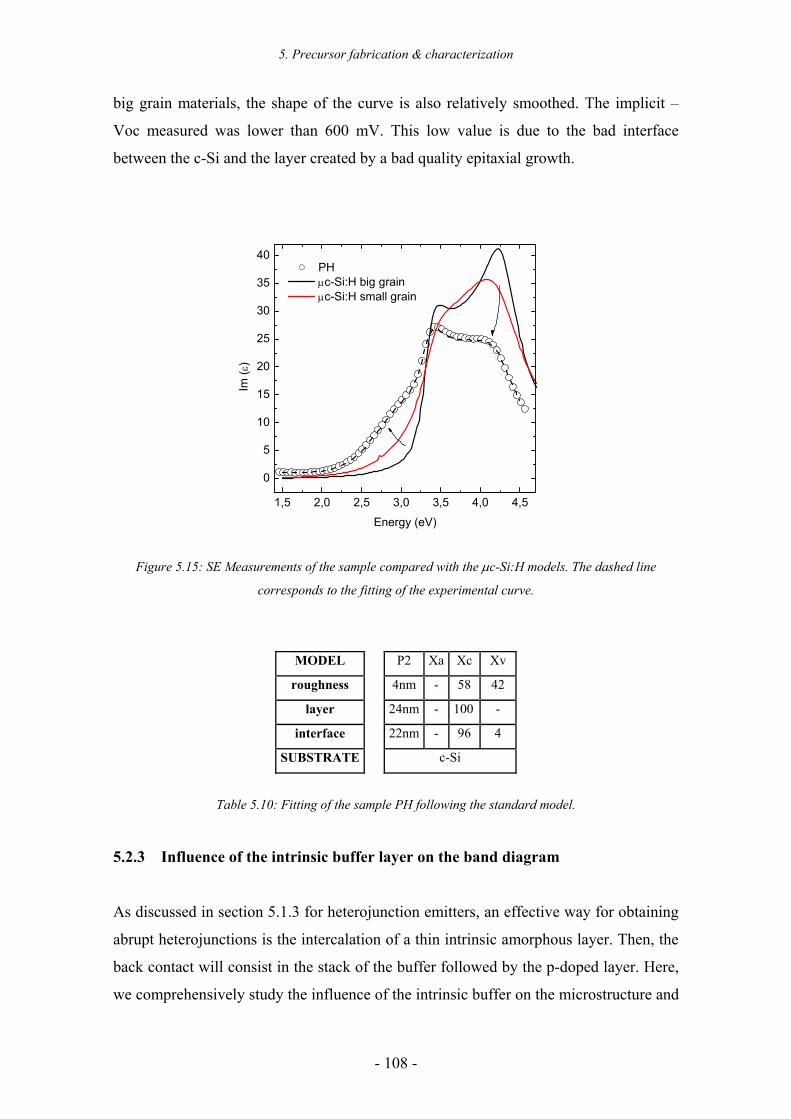
5. Precursor fabrication & characterization
- 108 -
big grain materials, the shape of the curve is also relatively smoothed. The implicit –
Voc measured was lower than 600 mV. This low value is due to the bad interface
between the c-Si and the layer created by a bad quality epitaxial growth.
1,5 2,0 2,5 3,0 3,5 4,0 4,5
0
5
10
15
20
25
30
35
40
Im
(ε)
Energy (eV)
PH µc-Si:H big grain µc-Si:H small grain
Figure 5.15: SE Measurements of the sample compared with the µc-Si:H models. The dashed line
corresponds to the fitting of the experimental curve.
MODEL P2 Xa Xc Xv
roughness 4nm - 58 42
layer 24nm - 100 -
interface 22nm - 96 4
SUBSTRATE c-Si
Table 5.10: Fitting of the sample PH following the standard model.
5.2.3 Influence of the intrinsic buffer layer on the band diagram
As discussed in section 5.1.3 for heterojunction emitters, an effective way for obtaining
abrupt heterojunctions is the intercalation of a thin intrinsic amorphous layer. Then, the
back contact will consist in the stack of the buffer followed by the p-doped layer. Here,
we comprehensively study the influence of the intrinsic buffer on the microstructure and
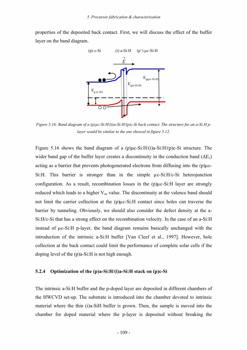
5. Precursor fabrication & characterization
- 109 -
properties of the deposited back contact. First, we will discuss the effect of the buffer
layer on the band diagram.
Eg (c-Si)
(p) c-Si (p+) µc-Si:H(i) a-Si:H
Eg(a-Si:H)
Eg(µc-Si:H)
→
E
Figure 5.16: Band diagram of a (p)µc-Si:H/(i)a-Si:H/(p)c-Si back contact. The structure for an a-Si:H p-
layer would be similar to the one showed in figure 5.12.
Figure 5.16 shows the band diagram of a (p)µc-Si:H/(i)a-Si:H/(p)c-Si structure. The
wider band gap of the buffer layer creates a discontinuity in the conduction band (∆Ec)
acting as a barrier that prevents photogenerated electrons from diffusing into the (p)µc-
Si:H. This barrier is stronger than in the simple µc-Si:H/c-Si heterojunction
configuration. As a result, recombination losses in the (p)µc-Si:H layer are strongly
reduced which leads to a higher Voc value. The discontinuity at the valence band should
not limit the carrier collection at the (p)µc-Si:H contact since holes can traverse the
barrier by tunneling. Obviously, we should also consider the defect density at the a-
Si:H/c-Si that has a strong effect on the recombination velocity. In the case of an a-Si:H
instead of µc-Si:H p-layer, the band diagram remains basically unchanged with the
introduction of the intrinsic a-Si:H buffer [Van Cleef et al., 1997]. However, hole
collection at the back contact could limit the performance of complete solar cells if the
doping level of the (p)a-Si:H is not high enough.
5.2.4 Optimization of the (p)a-Si:H/(i)a-Si:H stack on (p)c-Si
The intrinsic a-Si:H buffer and the p-doped layer are deposited in different chambers of
the HWCVD set-up. The substrate is introduced into the chamber devoted to intrinsic
material where the thin (i)a-SiH buffer is grown. Then, the sample is moved into the
chamber for doped material where the p-layer is deposited without breaking the
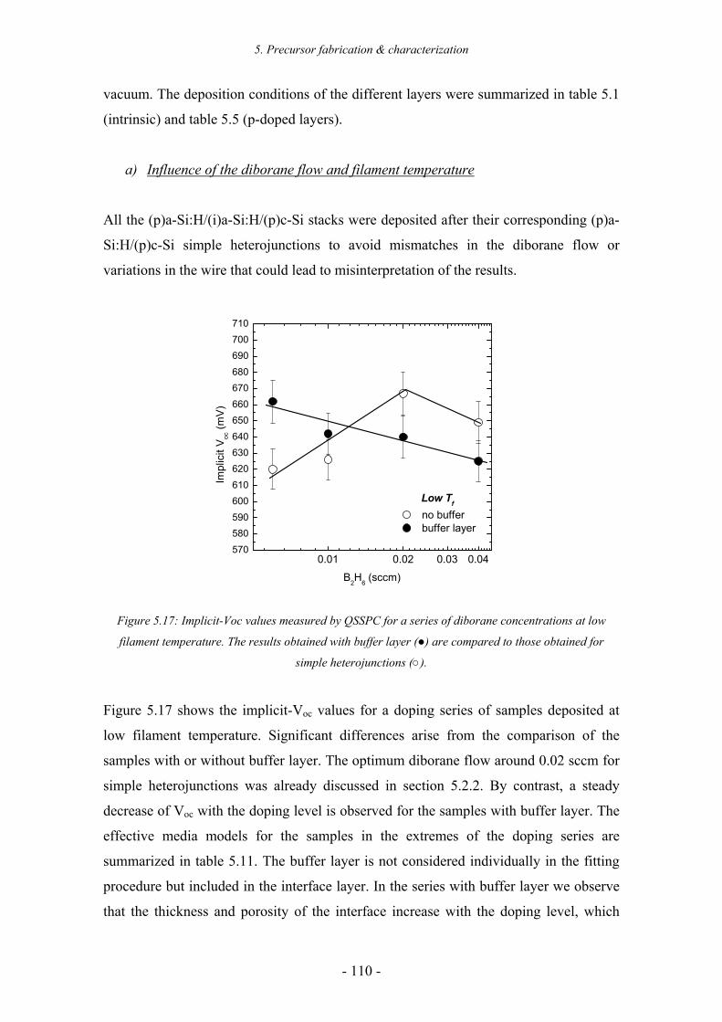
5. Precursor fabrication & characterization
- 110 -
vacuum. The deposition conditions of the different layers were summarized in table 5.1
(intrinsic) and table 5.5 (p-doped layers).
a) Influence of the diborane flow and filament temperature
All the (p)a-Si:H/(i)a-Si:H/(p)c-Si stacks were deposited after their corresponding (p)a-
Si:H/(p)c-Si simple heterojunctions to avoid mismatches in the diborane flow or
variations in the wire that could lead to misinterpretation of the results.
0.01 0.02 0.03 0.04570580590600610620630640650660670680690700710
Low Tf
no buffer buffer layer
Impl
icit
Voc
(mV
)
B2H6 (sccm)
Figure 5.17: Implicit-Voc values measured by QSSPC for a series of diborane concentrations at low
filament temperature. The results obtained with buffer layer () are compared to those obtained for
simple heterojunctions ().
Figure 5.17 shows the implicit-Voc values for a doping series of samples deposited at
low filament temperature. Significant differences arise from the comparison of the
samples with or without buffer layer. The optimum diborane flow around 0.02 sccm for
simple heterojunctions was already discussed in section 5.2.2. By contrast, a steady
decrease of Voc with the doping level is observed for the samples with buffer layer. The
effective media models for the samples in the extremes of the doping series are
summarized in table 5.11. The buffer layer is not considered individually in the fitting
procedure but included in the interface layer. In the series with buffer layer we observe
that the thickness and porosity of the interface increase with the doping level, which
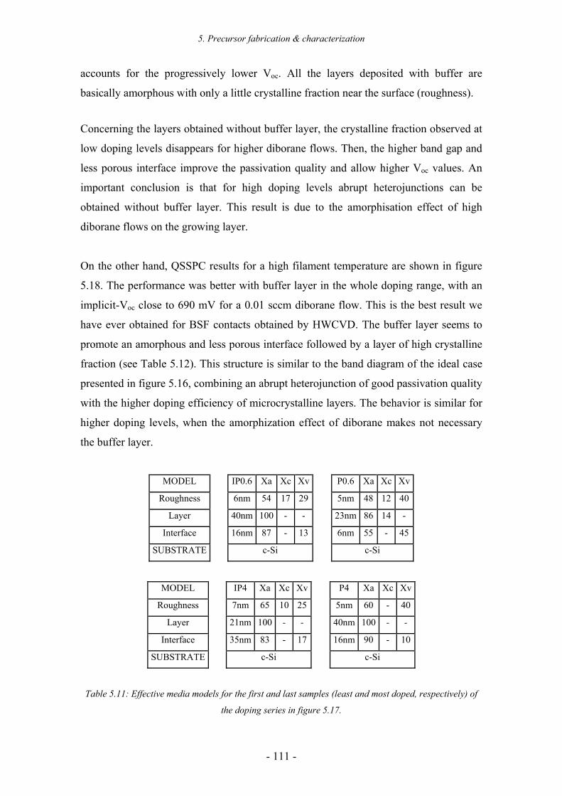
5. Precursor fabrication & characterization
- 111 -
accounts for the progressively lower Voc. All the layers deposited with buffer are
basically amorphous with only a little crystalline fraction near the surface (roughness).
Concerning the layers obtained without buffer layer, the crystalline fraction observed at
low doping levels disappears for higher diborane flows. Then, the higher band gap and
less porous interface improve the passivation quality and allow higher Voc values. An
important conclusion is that for high doping levels abrupt heterojunctions can be
obtained without buffer layer. This result is due to the amorphisation effect of high
diborane flows on the growing layer.
On the other hand, QSSPC results for a high filament temperature are shown in figure
5.18. The performance was better with buffer layer in the whole doping range, with an
implicit-Voc close to 690 mV for a 0.01 sccm diborane flow. This is the best result we
have ever obtained for BSF contacts obtained by HWCVD. The buffer layer seems to
promote an amorphous and less porous interface followed by a layer of high crystalline
fraction (see Table 5.12). This structure is similar to the band diagram of the ideal case
presented in figure 5.16, combining an abrupt heterojunction of good passivation quality
with the higher doping efficiency of microcrystalline layers. The behavior is similar for
higher doping levels, when the amorphization effect of diborane makes not necessary
the buffer layer.
MODEL IP0.6 Xa Xc Xv P0.6 Xa Xc Xv
Roughness 6nm 54 17 29 5nm 48 12 40
Layer 40nm 100 - - 23nm 86 14 -
Interface 16nm 87 - 13 6nm 55 - 45
SUBSTRATE c-Si c-Si
MODEL IP4 Xa Xc Xv P4 Xa Xc Xv
Roughness 7nm 65 10 25 5nm 60 - 40
Layer 21nm 100 - - 40nm 100 - -
Interface 35nm 83 - 17 16nm 90 - 10
SUBSTRATE c-Si c-Si
Table 5.11: Effective media models for the first and last samples (least and most doped, respectively) of
the doping series in figure 5.17.
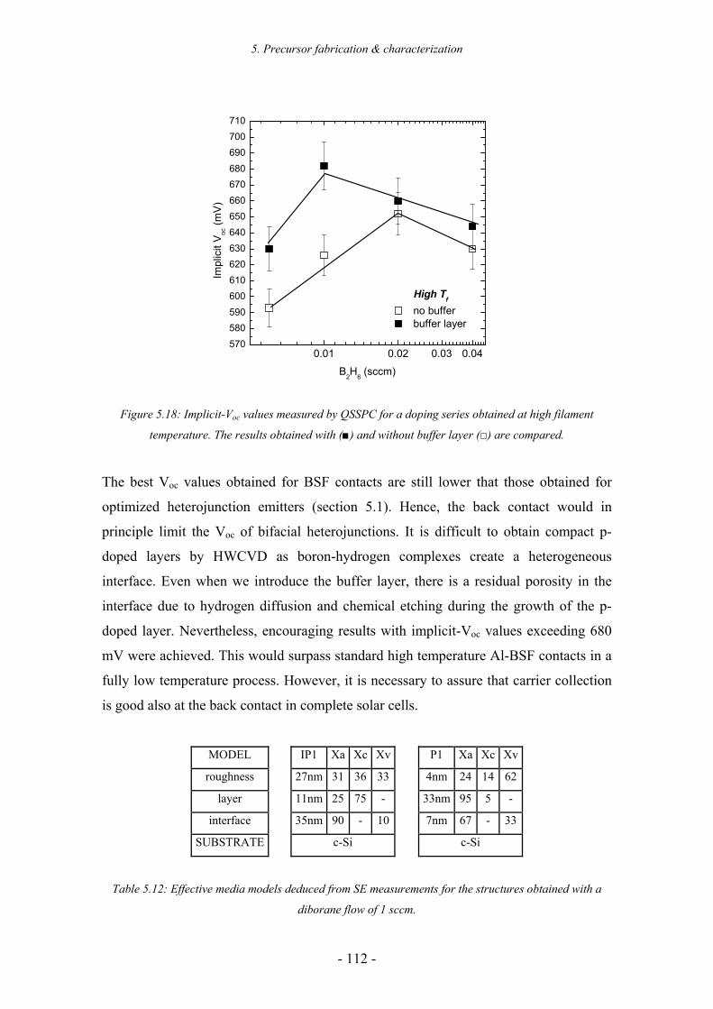
5. Precursor fabrication & characterization
- 112 -
0.01 0.02 0.03 0.04570580590600610620630640650660670680690700710
High Tf
no buffer buffer layer
Impl
icit
Voc
(mV
)
B2H6 (sccm)
Figure 5.18: Implicit-Voc values measured by QSSPC for a doping series obtained at high filament
temperature. The results obtained with () and without buffer layer () are compared.
The best Voc values obtained for BSF contacts are still lower that those obtained for
optimized heterojunction emitters (section 5.1). Hence, the back contact would in
principle limit the Voc of bifacial heterojunctions. It is difficult to obtain compact p-
doped layers by HWCVD as boron-hydrogen complexes create a heterogeneous
interface. Even when we introduce the buffer layer, there is a residual porosity in the
interface due to hydrogen diffusion and chemical etching during the growth of the p-
doped layer. Nevertheless, encouraging results with implicit-Voc values exceeding 680
mV were achieved. This would surpass standard high temperature Al-BSF contacts in a
fully low temperature process. However, it is necessary to assure that carrier collection
is good also at the back contact in complete solar cells.
MODEL IP1 Xa Xc Xv P1 Xa Xc Xv
roughness 27nm 31 36 33 4nm 24 14 62
layer 11nm 25 75 - 33nm 95 5 -
interface 35nm 90 - 10 7nm 67 - 33
SUBSTRATE c-Si c-Si
Table 5.12: Effective media models deduced from SE measurements for the structures obtained with a
diborane flow of 1 sccm.
6. Fabrication technologies of heterojunction solar cells
- 113 -
Chapter 6: Fabrication
technologies of heterojunction
solar cells
Desde que el hombre existe ha habido música, pero también
los animales, los átomos y las estrellas hacen música.
K. Stockhausen
¿porqué no las HIT?
This chapter deals with the technological issues related to the fabrication of complete
heterojunction solar cells. Aspects such as the optimization of the antireflection coating,
active area definition and the metallic grid electrode are reviewed in detail. The
characteristics of the best heterojunction solar cells fabricated during this thesis will be
also presented and discussed.
6.1. Optimization of the front TCO
Transparent conductive oxide (TCO) layers, which are both transparent in the visible
range and electrically conducting, have been widely studied for over 25 years [Nath et
al., 1980], [Ray et al., 1983]. Such particular properties have led to extensive
applications in optoelectronic devices. Among other alternatives, tin-doped indium
oxide, generally referred as indium-tin-oxide (ITO), and aluminium-doped zinc oxide
(AZO) are usual TCO layers. The high n-type conductivity of these films (> 103 Ω-1
6. Fabrication technologies of heterojunction solar cells
- 114 -
cm-1) results from a stoichiometric deviation (oxygen vacancies) and doping with excess
metal ions [Chen et al., 2000]. Although for thin film solar cells AZO is a very common
TCO, in a-Si:H/c-Si heterojunction solar cells most groups use ITO for the front
electrode. The reasons are the good properties in terms of conductivity and
transmittance, together with its adequate work function [Centurioni et al., 2003], as we
will discuss later.
In this work, we have optimized ITO layers obtained by RF sputtering magnetron in a
system with base pressure of 10-5 mbar. These layers are deposited on the emitter and
also on the BSF contact of bifacial solar cells. The substrate is located at a distance of 5
cm from the sintered target, which has an In2O3:SnO2 composition of 90:10wt.%. An
Argon flow of 10 sccm was used for the sputtering process at a pressure of 0.5 Pa.
Slight differences in the properties of the films were observed in the range 0.4-0.7 Pa.
6.1.1 Influence of the RF power
A series of samples varying the RF power from 30 to 150 W have been obtained at
room temperature. In figure 6.1, the resistivity and refraction index measured for these
samples are presented. As it is clearly observed, the resistivity of the films decreases for
high power values, whereas the refraction index behaves in the opposite direction. The
optimal values (of ρ ≈ 4×10⁻⁴ Ωcm) are obtained for high power values, but the optimum
refraction index n ≈ 2 is obtained in the 50 - 100 W range. Hence, the optimum power
considering both the resistivity and refraction index was 100 W which is the value used
from now in all the studied samples.
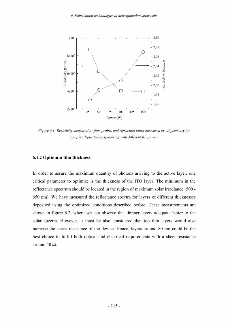
6. Fabrication technologies of heterojunction solar cells
- 115 -
25 50 75 100 125 1502x10-4
4x10⁻⁴
6x10⁻⁴
8x10⁻⁴
1x10⁻³
Res
istiv
ity (Ω
·cm
)
Power (W)
1,96
1,98
2,00
2,02
2,04
2,06
2,08
2,10
Ref
ract
ive
Inde
x, n
Figure 6.1: Resistivity measured by four-probes and refraction index measured by ellipsometry for
samples deposited by sputtering with different RF power.
6.1.2 Optimum film thickness
In order to assure the maximum quantity of photons arriving to the active layer, one
critical parameter to optimize is the thickness of the ITO layer. The minimum in the
reflectance spectrum should be located in the region of maximum solar irradiance (500 -
650 nm). We have measured the reflectance spectra for layers of different thicknesses
deposited using the optimized conditions described before. These measurements are
shown in figure 6.2, where we can observe that thinner layers adequate better to the
solar spectra. However, it must be also considered that too thin layers would also
increase the series resistance of the device. Hence, layers around 80 nm could be the
best choice to fulfill both optical and electrical requirements with a sheet resistance
around 50 Ω.
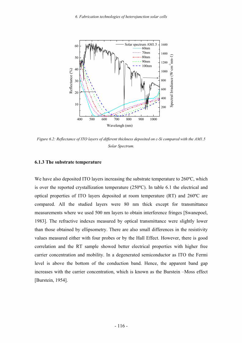
6. Fabrication technologies of heterojunction solar cells
- 116 -
400 500 600 700 800 900 1000
10
20
30
40
50
60 60nm 70nm 80nm 90nm 100nm
Ref
lect
ance
(%)
Wavelengh (nm)
200
400
600
800
1000
1200
1400
1600 Solar spectrum AM1.5
Spe
ctra
l Irr
adia
nce
(W·c
m-2nm
-1)
Figure 6.2: Reflectance of ITO layers of different thickness deposited on c-Si compared with the AM1.5
Solar Spectrum.
6.1.3 The substrate temperature
We have also deposited ITO layers increasing the substrate temperature to 260ºC, which
is over the reported crystallization temperature (250ºC). In table 6.1 the electrical and
optical properties of ITO layers deposited at room temperature (RT) and 260ºC are
compared. All the studied layers were 80 nm thick except for transmittance
measurements where we used 500 nm layers to obtain interference fringes [Swanepoel,
1983]. The refractive indexes measured by optical transmittance were slightly lower
than those obtained by ellipsometry. There are also small differences in the resistivity
values measured either with four probes or by the Hall Effect. However, there is good
correlation and the RT sample showed better electrical properties with higher free
carrier concentration and mobility. In a degenerated semiconductor as ITO the Fermi
level is above the bottom of the conduction band. Hence, the apparent band gap
increases with the carrier concentration, which is known as the Burstein –Moss effect
[Burstein, 1954].
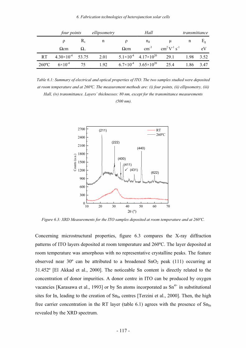
6. Fabrication technologies of heterojunction solar cells
- 117 -
four points ellipsometry Hall transmittance
ρ Rs n ρ nd µ n Eg
Ωcm Ω Ωcm cm-3 cm2 V-1 s-1 eV
RT 4.30×10⁻⁴ 53.75 2.01 5.1×10⁻⁴ 4.17×10²⁰ 29.1 1.98 3.52
260ºC 6×10⁻⁴ 75 1.92 6.7×10⁻⁴ 3.65×10²⁰ 25.4 1.86 3.47
Table 6.1: Summary of electrical and optical properties of ITO. The two samples studied were deposited
at room temperature and at 260ªC. The measurement methods are: (i) four points, (ii) ellipsometry, (iii)
Hall, (iv) transmittance. Layers´ thicknesses: 80 nm, except for the transmittance measurements
(500 nm).
10 20 30 40 50 60 700
300
600
900
1200
1500
1800
2100
2400
2700
(440)
(431)(622)
(411)
(400)
(222)
(211)
Cou
nts (
a.u.
)
RT 260ºC
2θ (º) Figure 6.3: XRD Measurements for the ITO samples deposited at room temperature and at 260ºC.
Concerning microstructural properties, figure 6.3 compares the X-ray diffraction
patterns of ITO layers deposited at room temperature and 260ºC. The layer deposited at
room temperature was amorphous with no representative crystalline peaks. The feature
observed near 30º can be attributed to a broadened SnO2 peak (111) occurring at
31.452º [El Akkad et al., 2000]. The noticeable Sn content is directly related to the
concentration of donor impurities. A donor centre in ITO can be produced by oxygen
vacancies [Karasawa et al., 1993] or by Sn atoms incorporated as Sn4+ in substitutional
sites for In, leading to the creation of SnIn centres [Terzini et al., 2000]. Then, the high
free carrier concentration in the RT layer (table 6.1) agrees with the presence of SnIn
revealed by the XRD spectrum.
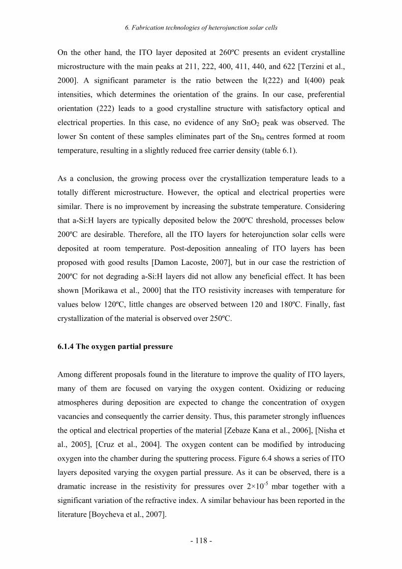
6. Fabrication technologies of heterojunction solar cells
- 118 -
On the other hand, the ITO layer deposited at 260ºC presents an evident crystalline
microstructure with the main peaks at 211, 222, 400, 411, 440, and 622 [Terzini et al.,
2000]. A significant parameter is the ratio between the I(222) and I(400) peak
intensities, which determines the orientation of the grains. In our case, preferential
orientation (222) leads to a good crystalline structure with satisfactory optical and
electrical properties. In this case, no evidence of any SnO2 peak was observed. The
lower Sn content of these samples eliminates part of the SnIn centres formed at room
temperature, resulting in a slightly reduced free carrier density (table 6.1).
As a conclusion, the growing process over the crystallization temperature leads to a
totally different microstructure. However, the optical and electrical properties were
similar. There is no improvement by increasing the substrate temperature. Considering
that a-Si:H layers are typically deposited below the 200ºC threshold, processes below
200ºC are desirable. Therefore, all the ITO layers for heterojunction solar cells were
deposited at room temperature. Post-deposition annealing of ITO layers has been
proposed with good results [Damon Lacoste, 2007], but in our case the restriction of
200ºC for not degrading a-Si:H layers did not allow any beneficial effect. It has been
shown [Morikawa et al., 2000] that the ITO resistivity increases with temperature for
values below 120ºC, little changes are observed between 120 and 180ºC. Finally, fast
crystallization of the material is observed over 250ºC.
6.1.4 The oxygen partial pressure
Among different proposals found in the literature to improve the quality of ITO layers,
many of them are focused on varying the oxygen content. Oxidizing or reducing
atmospheres during deposition are expected to change the concentration of oxygen
vacancies and consequently the carrier density. Thus, this parameter strongly influences
the optical and electrical properties of the material [Zebaze Kana et al., 2006], [Nisha et
al., 2005], [Cruz et al., 2004]. The oxygen content can be modified by introducing
oxygen into the chamber during the sputtering process. Figure 6.4 shows a series of ITO
layers deposited varying the oxygen partial pressure. As it can be observed, there is a
dramatic increase in the resistivity for pressures over 2×10⁻⁵ mbar together with a
significant variation of the refractive index. A similar behaviour has been reported in the
literature [Boycheva et al., 2007].
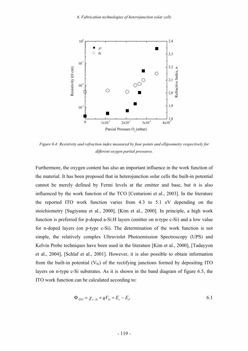
6. Fabrication technologies of heterojunction solar cells
- 119 -
0 1x10⁻⁵ 2x10⁻⁵ 3x10⁻⁵ 4x10⁻⁵
10-3
10-2
10-1
100
Res
istiv
ity (Ω
·cm
)
Parcial Pressure O2 (mbar)
ρ
1,8
1,9
2,0
2,1
2,2
2,3
2,4
Ref
ract
ive
Inde
x, n
n
Figure 6.4: Resistivity and refraction index measured by four points and ellipsometry respectively for
different oxygen partial pressures.
Furthermore, the oxygen content has also an important influence in the work function of
the material. It has been proposed that in heterojunction solar cells the built-in potential
cannot be merely defined by Fermi levels at the emitter and base, but it is also
influenced by the work function of the TCO [Centurioni et al., 2003]. In the literature
the reported ITO work function varies from 4.3 to 5.1 eV depending on the
stoichiometry [Sugiyama et al., 2000], [Kim et al., 2000]. In principle, a high work
function is preferred for p-doped a-Si:H layers (emitter on n-type c-Si) and a low value
for n-doped layers (on p-type c-Si). The determination of the work function is not
simple, the relatively complex Ultraviolet Photoemission Spectroscopy (UPS) and
Kelvin Probe techniques have been used in the literature [Kim et al., 2000], [Tadayyon
et al., 2004], [Schlaf et al., 2001]. However, it is also possible to obtain information
from the built-in potential (Vbi) of the rectifying junctions formed by depositing ITO
layers on n-type c-Si substrates. As it is shown in the band diagram of figure 6.5, the
ITO work function can be calculated according to:
FcbiSicITO EEqV −++=Φ −χ 6.1
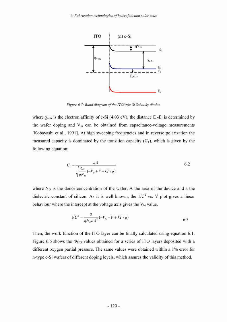
6. Fabrication technologies of heterojunction solar cells
- 120 -
Figure 6.5: Band diagram of the ITO/(n)c-Si Schottky diodes.
where χc-Si is the electron affinity of c-Si (4.03 eV), the distance Ec-Ef is determined by
the wafer doping and Vbi can be obtained from capacitance-voltage measurements
[Kobayashi et al., 1991]. At high sweeping frequencies and in reverse polarization the
measured capacity is dominated by the transition capacity (CT), which is given by the
following equation:
where ND is the donor concentration of the wafer, A the area of the device and ε the
dielectric constant of silicon. As it is well known, the 1/C2 vs. V plot gives a linear
behaviour where the intercept at the voltage axis gives the Vbi value.
Then, the work function of the ITO layer can be finally calculated using equation 6.1.
Figure 6.6 shows the ΦITO values obtained for a series of ITO layers deposited with a
different oxygen partial pressure. The same values were obtained within a 1% error for
n-type c-Si wafers of different doping levels, which assures the validity of this method.
ITO (n) c-Si
Ev
E0
Ec
ΦITO χc-Si
qVbi
Ec-Ef
Ef
6.2 2 ( / )
T
biD
ACV V kT q
qN
εε
=− + +
22
21 ( / )biD
C V V kT qqN Aε
= − + + 6.3
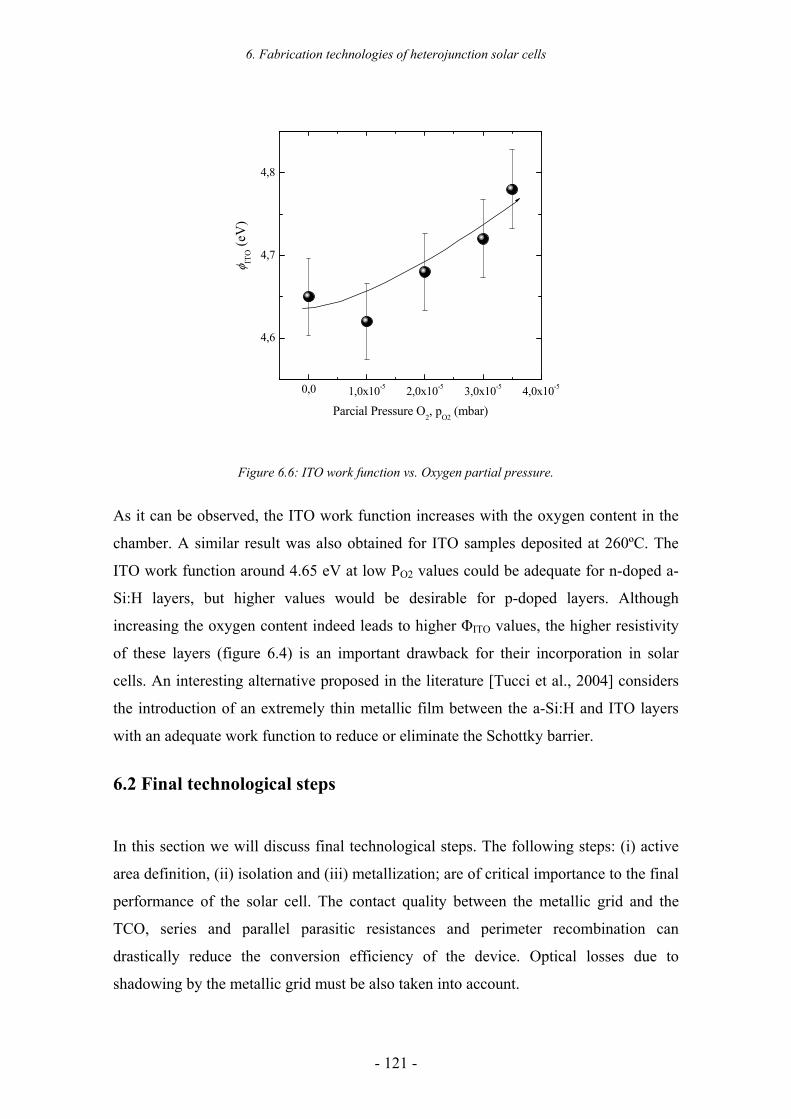
6. Fabrication technologies of heterojunction solar cells
- 121 -
0,0 1,0x10⁻⁵ 2,0x10⁻⁵ 3,0x10⁻⁵ 4,0x10⁻⁵
4,6
4,7
4,8
φ ITO (e
V)
Parcial Pressure O2, pO2 (mbar)
Figure 6.6: ITO work function vs. Oxygen partial pressure.
As it can be observed, the ITO work function increases with the oxygen content in the
chamber. A similar result was also obtained for ITO samples deposited at 260ºC. The
ITO work function around 4.65 eV at low PO2 values could be adequate for n-doped a-
Si:H layers, but higher values would be desirable for p-doped layers. Although
increasing the oxygen content indeed leads to higher ΦITO values, the higher resistivity
of these layers (figure 6.4) is an important drawback for their incorporation in solar
cells. An interesting alternative proposed in the literature [Tucci et al., 2004] considers
the introduction of an extremely thin metallic film between the a-Si:H and ITO layers
with an adequate work function to reduce or eliminate the Schottky barrier.
6.2 Final technological steps
In this section we will discuss final technological steps. The following steps: (i) active
area definition, (ii) isolation and (iii) metallization; are of critical importance to the final
performance of the solar cell. The contact quality between the metallic grid and the
TCO, series and parallel parasitic resistances and perimeter recombination can
drastically reduce the conversion efficiency of the device. Optical losses due to
shadowing by the metallic grid must be also taken into account.
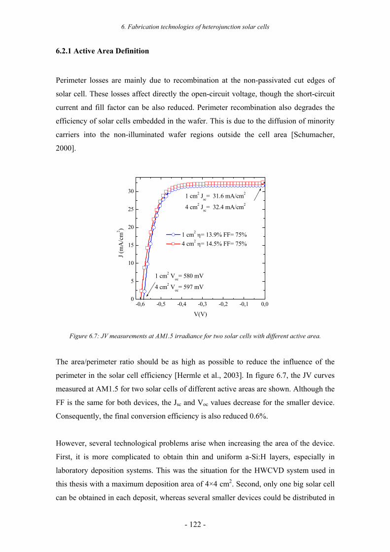
6. Fabrication technologies of heterojunction solar cells
- 122 -
6.2.1 Active Area Definition
Perimeter losses are mainly due to recombination at the non-passivated cut edges of
solar cell. These losses affect directly the open-circuit voltage, though the short-circuit
current and fill factor can be also reduced. Perimeter recombination also degrades the
efficiency of solar cells embedded in the wafer. This is due to the diffusion of minority
carriers into the non-illuminated wafer regions outside the cell area [Schumacher,
2000].
-0,6 -0,5 -0,4 -0,3 -0,2 -0,1 0,00
5
10
15
20
25
30
1 cm2 η= 13.9% FF= 75% 4 cm2 η= 14.5% FF= 75%
1 cm2 Voc= 580 mV
4 cm2 Voc= 597 mV
1 cm2 Jsc= 31.6 mA/cm2
4 cm2 Jsc= 32.4 mA/cm2
J (m
A/c
m2 )
V(V)
Figure 6.7: JV measurements at AM1.5 irradiance for two solar cells with different active area.
The area/perimeter ratio should be as high as possible to reduce the influence of the
perimeter in the solar cell efficiency [Hermle et al., 2003]. In figure 6.7, the JV curves
measured at AM1.5 for two solar cells of different active areas are shown. Although the
FF is the same for both devices, the Jsc and Voc values decrease for the smaller device.
Consequently, the final conversion efficiency is also reduced 0.6%.
However, several technological problems arise when increasing the area of the device.
First, it is more complicated to obtain thin and uniform a-Si:H layers, especially in
laboratory deposition systems. This was the situation for the HWCVD system used in
this thesis with a maximum deposition area of 4×4 cm2. Second, only one big solar cell
can be obtained in each deposit, whereas several smaller devices could be distributed in
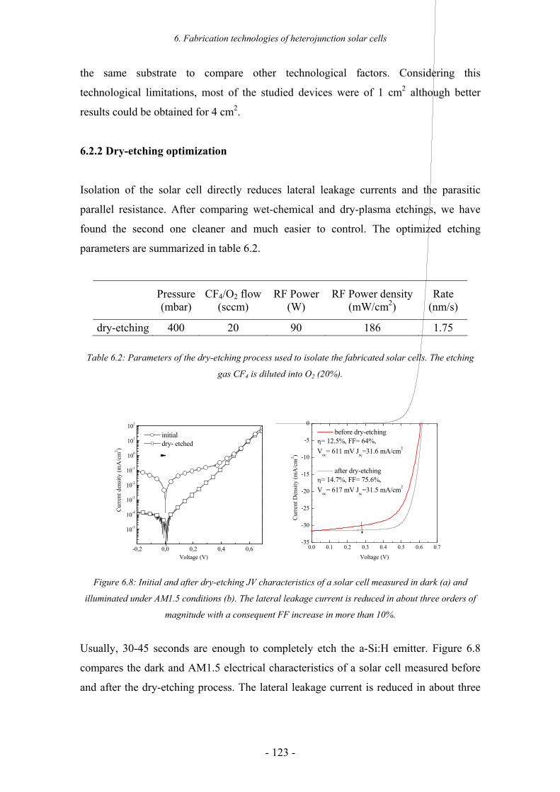
6. Fabrication technologies of heterojunction solar cells
- 123 -
the same substrate to compare other technological factors. Considering this
technological limitations, most of the studied devices were of 1 cm2 although better
results could be obtained for 4 cm2.
6.2.2 Dry-etching optimization
Isolation of the solar cell directly reduces lateral leakage currents and the parasitic
parallel resistance. After comparing wet-chemical and dry-plasma etchings, we have
found the second one cleaner and much easier to control. The optimized etching
parameters are summarized in table 6.2.
Pressure (mbar)
CF4/O2 flow (sccm)
RF Power (W)
RF Power density (mW/cm2)
Rate (nm/s)
dry-etching 400 20 90 186 1.75
Table 6.2: Parameters of the dry-etching process used to isolate the fabricated solar cells. The etching
gas CF4 is diluted into O2 (20%).
-0,2 0,0 0,2 0,4 0,6
10-5
10-4
10-3
10-2
10-1
100
101
102
initial dry- etched
Cur
rent
den
sity
(mA
/cm
2 )
Voltage (V)
0.0 0.1 0.2 0.3 0.4 0.5 0.6 0.7-35
-30
-25
-20
-15
-10
-5
0 before dry-etching
η= 12.5%, FF= 64%,Voc= 611 mV Jsc=31.6 mA/cm2
after dry-etchingη= 14.7%, FF= 75.6%, Voc= 617 mV Jsc=31.5 mA/cm2
Cur
rent
Den
sity
(mA
/cm
2 )
Voltage (V)
Figure 6.8: Initial and after dry-etching JV characteristics of a solar cell measured in dark (a) and
illuminated under AM1.5 conditions (b). The lateral leakage current is reduced in about three orders of
magnitude with a consequent FF increase in more than 10%.
Usually, 30-45 seconds are enough to completely etch the a-Si:H emitter. Figure 6.8
compares the dark and AM1.5 electrical characteristics of a solar cell measured before
and after the dry-etching process. The lateral leakage current is reduced in about three
6. Fabrication technologies of heterojunction solar cells
- 124 -
orders of magnitude, which leads to a FF value more than 10% higher. Then, the final
conversion efficiency was increased in more than 2% just insulating the device.
6.2.3 Metallization and grid optimization
The metallic grid is also of critical importance, since it can strongly affect the final solar
cell efficiency. A non-optimal finger layout or an excessive shadowing can cause
important optical and electrical losses. The basic metallization design follows an H-grid
pattern, although artistic designs have been also proposed to convert the busbar into an
eye-catching module feature [Radike et al., 1999]. Nevertheless, mathematical
calculation and simulation [Burgers, 1999], [Antonini et al., 2003] are generally used to
optimize the grid design for optimum carrier collection with as low as possible
shadowing. The length of the bus bar, the distance between the fingers and their
geometric distribution in the solar cell area are of critical importance. We can
distinguish three different power loss effects related to the metallic top contact: the
contact resistance between the metal and the ITO layer, the resistance of the metallic
fingers and, finally, the shadowed area [Cuevas et al., 2000]. These effects can be
quantified as relative power losses with respect to the maximum power point, that is,
p=Ploss/Pmp.
a) losses due to the contact resistance between the metal and the ITO layer
This power loss can be expressed as:
fmp
mpcc W
SVJ
p ρ=
where Jmp and Vmp are the current density and voltage values at the maximum power
point, S is the distance between fingers, Wf is the width of the fingers and ρc is the
specific contact resistance. The Jmp/Vmp ratio can be approximated by Jsc/Voc, which is
typically in the 0.055 - 0.06 Ωcm-2 range [Cuevas et al., 2000]. In this point we focus on
lowering the contact resistance between the metal and the ITO layer, while the S/Wf
6.4
6. Fabrication technologies of heterojunction solar cells
- 125 -
ratio will be considered later. We have deposited different metallic contacts (Ag, Au, Ti,
Cr, Al) on ITO layers to measure their corresponding contact resistances.
Ag Au Ti Cr Al0.01
0.1
1
10
Spec
ific
cont
act r
esis
tanc
e (Ω
cm2 )
Metal
as deposited after 30min 100ºC after 60min 100ºC
Figure 6.9: Specific contact resistance of different metallic contacts evaporated on ITO layers. The inset
shows the mask used for the evaporation process.
These results are shown in figure 6.9, together with the effect of post annealing at 100ºC
for different times. At first sight, chromium and aluminium evidenced a higher contact
resistance on ITO compared to silver, gold or titanium contacts. Among these, the
lowest contact resistance was obtained with titanium. Actually, an usual metallic contact
for crystalline silicon solar cells consists of three layers Ti/Pd/Ag consecutively
evaporated to obtain good adherence and low series resistance. However, titanium is
rather expensive and it always requires the evaporation of additional palladium/silver or
at least silver layers. By contrast, either silver or gold directly evaporated on ITO allow
quite satisfactory contact resistances of only 0.2 Ωcm2. In the case of gold, annealing at
100ºC even reduces the contact resistance below 0.1 Ωcm2. Nevertheless, the higher
cost of gold and the inconvenience of additional annealing steps make this option less
interesting. Therefore, silver can be considered a good choice in terms of the cost and
simplicity of the process.
1cm 1mm
6. Fabrication technologies of heterojunction solar cells
- 126 -
b) losses due to the resistance of the metallic fingers
This term can be expressed as:
fmp
mpmm W
SVJ
RBp 2
31
=
where B is the finger length and Rm the sheet resistance of the metal calculated as:
fm t
R ρ=
where ρ is the resistivity of the metal and tf the finger thickness. Figure 6.10 compares
the JV characteristics of two solar cells with silver fingers 0.1 and 1µm thick. As
expected, a clear improvement in the FF value is observed for the solar cell with thicker
metallic contact. Around open-circuit conditions the parasitic series resistance Rs can be
calculated supposing V≈IRs. Considering that the wafers were 300 µm thick with a
resistivity of 14 Ωcm, the bulk contribution of the c-Si substrate to the series resistance
is 0.42 Ωcm2. Then, taken into account that the ITO/Ag contact resistance is around 0.2
Ωcm2 (figure 6.9), the contribution of the fingers to the series resistance can be finally
calculated. These values are shown in table 6.3. We have neglected the contributions to
the series resistance related to the Al-BSF and ITO/a-Si:H contact which are, in
principle, much smaller.
tf Rs (total) Rs (wafer) Rs (TCO-Ag) Rs (finger) FF η nm Ωcm2 Ωcm2 Ωcm2 Ωcm2 % %
1000 1,5 0,42 0,2 0,88 74,5 14,6 100 2,9 0,42 0,2 2,28 68,4 13,2
Table 6.3: Summary of the resistive losses of solar cells fabricated using Al-BSF contacts. We have
neglected the Rs contribution due to the ITO/a-Si:H and Al-BSF contacts.
6.5
6.6
6. Fabrication technologies of heterojunction solar cells
- 127 -
0.0 0.1 0.2 0.3 0.4 0.5 0.6 0.7-35
-30
-25
-20
-15
-10
-5
0
ITO-Ag (1µm) ITO-Ag (100nm)
Cur
rent
Den
sity
(mA
/cm
2 )
Voltage (V)
Figure 6.10: JV characteristics measured in AM1.5 conditions for two heterojunction solar cell s on Al-
BSF with different Ag grid thicknesses.
Hence, the contribution of the fingers to the series resistance steadily decreases with the
thickness of evaporated silver. However, there are technological limitations related to
the adherence of silver on ITO layers. In addition, thicker metallic fingers become also
wider increasing shadowing losses.
c) losses due to shadowing by the metallic grid
Once the metal and its thickness have been chosen, the design of the metallic grid
basically consists in finding the optimum width and separation between fingers to
obtain the best compromise between resistive losses and optical shadowing. In
particular, the factor to take in consideration is:
SWp f
s =
which unfortunately appears inverted in the electrical factors pc and pm (equations 6.4-
6.6). Therefore, the optical ps factor should not be reduced below values that would
cause higher electrical losses. We have optimized the design of the metallic grid
6.7
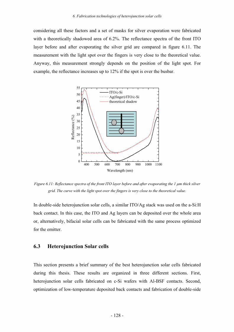
6. Fabrication technologies of heterojunction solar cells
- 128 -
considering all these factors and a set of masks for silver evaporation were fabricated
with a theoretically shadowed area of 6.2%. The reflectance spectra of the front ITO
layer before and after evaporating the silver grid are compared in figure 6.11. The
measurement with the light spot over the fingers is very close to the theoretical value.
Anyway, this measurement strongly depends on the position of the light spot. For
example, the reflectance increases up to 12% if the spot is over the busbar.
400 500 600 700 800 900 1000 11000
5
10
15
20
25
30
35
40
45
50
55
Ref
lect
ance
(%)
Wavelength (nm)
ITO/c-Si Ag(finger)/ITO/c-Si theoretical shadow
Figure 6.11: Reflectance spectra of the front ITO layer before and after evaporating the 1 µm thick silver
grid. The curve with the light spot over the fingers is very close to the theoretical value.
In double-side heterojunction solar cells, a similar ITO/Ag stack was used on the a-Si:H
back contact. In this case, the ITO and Ag layers can be deposited over the whole area
or, alternatively, bifacial solar cells can be fabricated with the same process optimized
for the emitter.
6.3 Heterojunction Solar cells
This section presents a brief summary of the best heterojunction solar cells fabricated
during this thesis. These results are organized in three different sections. First,
heterojunction solar cells fabricated on c-Si wafers with Al-BSF contacts. Second,
optimization of low-temperature deposited back contacts and fabrication of double-side
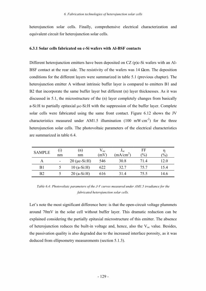
6. Fabrication technologies of heterojunction solar cells
- 129 -
heterojunction solar cells. Finally, comprehensive electrical characterization and
equivalent circuit for heterojunction solar cells.
6.3.1 Solar cells fabricated on c-Si wafers with Al-BSF contacts
Different heterojunction emitters have been deposited on CZ (p)c-Si wafers with an Al-
BSF contact at the rear side. The resistivity of the wafers was 14 Ωcm. The deposition
conditions for the different layers were summarized in table 5.1 (previous chapter). The
heterojunction emitter A without intrinsic buffer layer is compared to emitters B1 and
B2 that incorporate the same buffer layer but different (n) layer thicknesses. As it was
discussed in 5.1, the microstructure of the (n) layer completely changes from basically
a-Si:H to partially epitaxial µc-Si:H with the suppression of the buffer layer. Complete
solar cells were fabricated using the same front contact. Figure 6.12 shows the JV
characteristics measured under AM1.5 illumination (100 mW⋅cm-2) for the three
heterojunction solar cells. The photovoltaic parameters of the electrical characteristics
are summarized in table 6.4.
SAMPLE (i) nm
(n) nm
Voc (mV)
Jsc (mA/cm2)
FF (%)
η (%)
A - 20 (µc-Si:H) 546 30.8 71.4 12.0 B1 5 10 (a-Si:H) 622 32.7 75.7 15.4 B2 5 20 (a-Si:H) 616 31.4 75.5 14.6
Table 6.4: Photovoltaic parameters of the J-V curves measured under AM1.5 irradiance for the
fabricated heterojunction solar cells.
Let’s note the most significant difference here: is that the open-circuit voltage plummets
around 70mV in the solar cell without buffer layer. This dramatic reduction can be
explained considering the partially epitaxial microstructure of this emitter. The absence
of heterojunction reduces the built-in voltage and, hence, also the Voc value. Besides,
the passivation quality is also degraded due to the increased interface porosity, as it was
deduced from ellipsometry measurements (section 5.1.3).
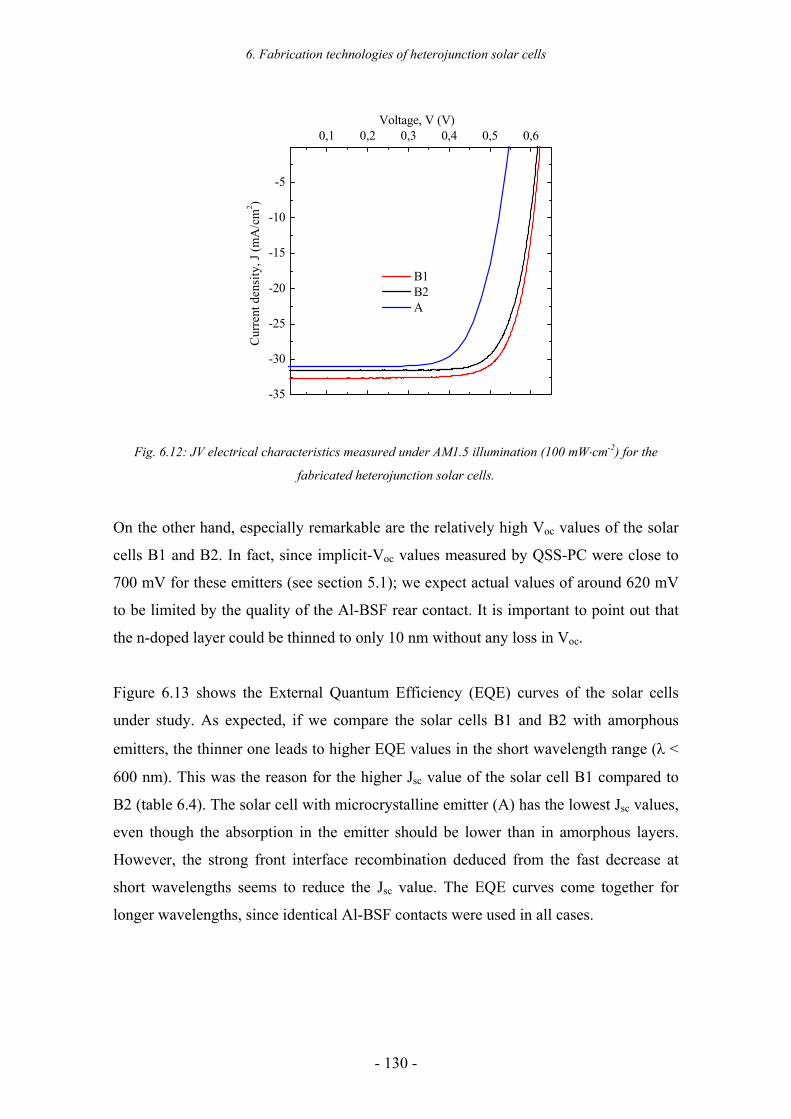
6. Fabrication technologies of heterojunction solar cells
- 130 -
0,1 0,2 0,3 0,4 0,5 0,6
-35
-30
-25
-20
-15
-10
-5
B1 B2 A
Cur
rent
den
sity
, J (m
A/c
m2 )
Voltage, V (V)
Fig. 6.12: JV electrical characteristics measured under AM1.5 illumination (100 mW⋅cm-2) for the
fabricated heterojunction solar cells.
On the other hand, especially remarkable are the relatively high Voc values of the solar
cells B1 and B2. In fact, since implicit-Voc values measured by QSS-PC were close to
700 mV for these emitters (see section 5.1); we expect actual values of around 620 mV
to be limited by the quality of the Al-BSF rear contact. It is important to point out that
the n-doped layer could be thinned to only 10 nm without any loss in Voc.
Figure 6.13 shows the External Quantum Efficiency (EQE) curves of the solar cells
under study. As expected, if we compare the solar cells B1 and B2 with amorphous
emitters, the thinner one leads to higher EQE values in the short wavelength range (λ <
600 nm). This was the reason for the higher Jsc value of the solar cell B1 compared to
B2 (table 6.4). The solar cell with microcrystalline emitter (A) has the lowest Jsc values,
even though the absorption in the emitter should be lower than in amorphous layers.
However, the strong front interface recombination deduced from the fast decrease at
short wavelengths seems to reduce the Jsc value. The EQE curves come together for
longer wavelengths, since identical Al-BSF contacts were used in all cases.
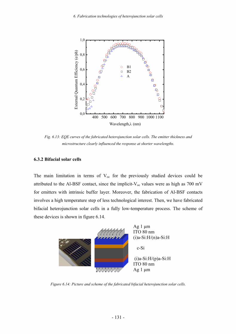
6. Fabrication technologies of heterojunction solar cells
- 131 -
400 500 600 700 800 900 1000 11000,0
0,2
0,4
0,6
0,8
1,0
B1 B2 A
Exte
rnal
Qua
ntum
Eff
icie
ncy
(e/p
h)
Wavelength,λ (nm)
Fig. 6.13: EQE curves of the fabricated heterojunction solar cells. The emitter thickness and
microstructure clearly influenced the response at shorter wavelengths.
6.3.2 Bifacial solar cells
The main limitation in terms of Voc for the previously studied devices could be
attributed to the Al-BSF contact, since the implicit-Voc values were as high as 700 mV
for emitters with intrinsic buffer layer. Moreover, the fabrication of Al-BSF contacts
involves a high temperature step of less technological interest. Then, we have fabricated
bifacial heterojunction solar cells in a fully low-temperature process. The scheme of
these devices is shown in figure 6.14.
Figure 6.14: Picture and scheme of the fabricated bifacial heterojunction solar cells.
Ag 1 µm ITO 80 nm (i)a-Si:H/(n)a-Si:H
(i)a-Si:H/(p)a-Si:H ITO 80 nm Ag 1 µm
c-Si
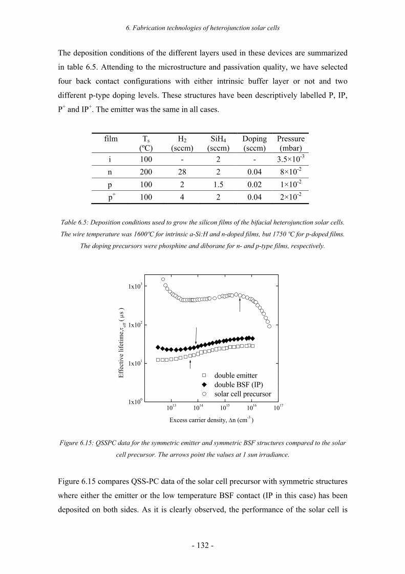
6. Fabrication technologies of heterojunction solar cells
- 132 -
The deposition conditions of the different layers used in these devices are summarized
in table 6.5. Attending to the microstructure and passivation quality, we have selected
four back contact configurations with either intrinsic buffer layer or not and two
different p-type doping levels. These structures have been descriptively labelled P, IP,
P+ and IP+. The emitter was the same in all cases.
film
Ts (ºC)
H2 (sccm)
SiH4 (sccm)
Doping (sccm)
Pressure (mbar)
i 100 - 2 - 3.5×10⁻³ n 200 28 2 0.04 8×10⁻² p 100 2 1.5 0.02 1×10⁻²
p+ 100 4 2 0.04 2×10⁻² Table 6.5: Deposition conditions used to grow the silicon films of the bifacial heterojunction solar cells.
The wire temperature was 1600ºC for intrinsic a-Si:H and n-doped films, but 1750 ºC for p-doped films.
The doping precursors were phosphine and diborane for n- and p-type films, respectively.
1013 1014 1015 1016 10171x100
1x101
1x10²
1x10³
Effe
ctiv
e lif
etim
e,τ ef
f ( µs
)
Excess carrier density, ∆n (cm-3 )
double emitter double BSF (IP) solar cell precursor
Figure 6.15: QSSPC data for the symmetric emitter and symmetric BSF structures compared to the solar
cell precursor. The arrows point the values at 1 sun irradiance.
Figure 6.15 compares QSS-PC data of the solar cell precursor with symmetric structures
where either the emitter or the low temperature BSF contact (IP in this case) has been
deposited on both sides. As it is clearly observed, the performance of the solar cell is
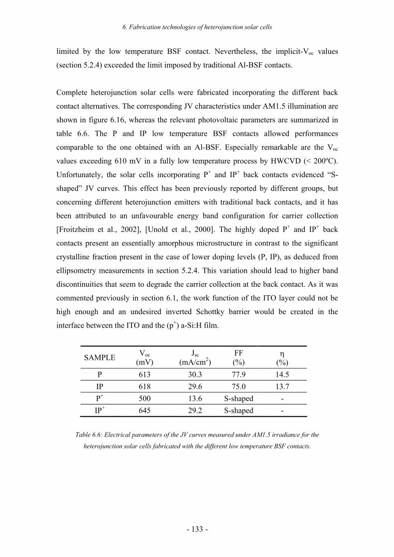
6. Fabrication technologies of heterojunction solar cells
- 133 -
limited by the low temperature BSF contact. Nevertheless, the implicit-Voc values
(section 5.2.4) exceeded the limit imposed by traditional Al-BSF contacts.
Complete heterojunction solar cells were fabricated incorporating the different back
contact alternatives. The corresponding JV characteristics under AM1.5 illumination are
shown in figure 6.16, whereas the relevant photovoltaic parameters are summarized in
table 6.6. The P and IP low temperature BSF contacts allowed performances
comparable to the one obtained with an Al-BSF. Especially remarkable are the Voc
values exceeding 610 mV in a fully low temperature process by HWCVD (< 200ºC).
Unfortunately, the solar cells incorporating P+ and IP+ back contacts evidenced “S-
shaped” JV curves. This effect has been previously reported by different groups, but
concerning different heterojunction emitters with traditional back contacts, and it has
been attributed to an unfavourable energy band configuration for carrier collection
[Froitzheim et al., 2002], [Unold et al., 2000]. The highly doped P+ and IP+ back
contacts present an essentially amorphous microstructure in contrast to the significant
crystalline fraction present in the case of lower doping levels (P, IP), as deduced from
ellipsometry measurements in section 5.2.4. This variation should lead to higher band
discontinuities that seem to degrade the carrier collection at the back contact. As it was
commented previously in section 6.1, the work function of the ITO layer could not be
high enough and an undesired inverted Schottky barrier would be created in the
interface between the ITO and the (p+) a-Si:H film.
SAMPLE Voc (mV)
Jsc (mA/cm2)
FF (%)
η (%)
P 613 30.3 77.9 14.5 IP 618 29.6 75.0 13.7 P+ 500 13.6 S-shaped - IP+ 645 29.2 S-shaped -
Table 6.6: Electrical parameters of the JV curves measured under AM1.5 irradiance for the
heterojunction solar cells fabricated with the different low temperature BSF contacts.
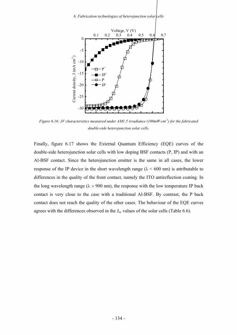
6. Fabrication technologies of heterojunction solar cells
- 134 -
-30
-25
-20
-15
-10
-5
00.1 0.2 0.3 0.4 0.5 0.6 0.7
P+
IP+
P IP
Voltage, V (V)
Cur
rent
den
sity
, J (m
A c
m-2
)
Figure 6.16: JV characteristics measured under AM1.5 irradiance (100mW⋅cm-2) for the fabricated
double-side heterojunction solar cells.
Finally, figure 6.17 shows the External Quantum Efficiency (EQE) curves of the
double-side heterojunction solar cells with low doping BSF contacts (P, IP) and with an
Al-BSF contact. Since the heterojunction emitter is the same in all cases, the lower
response of the IP device in the short wavelength range (λ < 600 nm) is attributable to
differences in the quality of the front contact, namely the ITO antireflection coating. In
the long wavelength range (λ > 900 nm), the response with the low temperature IP back
contact is very close to the case with a traditional Al-BSF. By contrast, the P back
contact does not reach the quality of the other cases. The behaviour of the EQE curves
agrees with the differences observed in the Jsc values of the solar cells (Table 6.6).
6. Fabrication technologies of heterojunction solar cells
- 135 -
300 400 500 600 700 800 900 1000 11000.0
0.1
0.2
0.3
0.4
0.5
0.6
0.7
0.8
0.9
1.0
P IP Al-BSF
Exte
rnal
Qua
ntum
Eff
icie
ncy,
EQ
E (e
/ph)
Wavelength, λ (nm) Figure 6.17: External Quantum Efficiency curves of the double-side heterojunction solar cells with P and
IP BSF contacts compared to the case with a traditional Al-BSF contact.
6.3.3 Equivalent circuit and thermal dependence of the electrical characteristics
The best bifacial heterojunction solar cell on p-type c-Si was reproduced on n-type
substrates as a first approach to the complementary technology. The JV characteristics
of both cells have been measured under AM1.5 conditions (100 Wcm-2) for front and
rear side illumination. The measured curves are shown in figure 6.18 and the resulting
photovoltaic parameters have been summarized in table 6.7.
Two important conclusions can be extracted from these results. On the one hand, it is
remarkable the photovoltaic response obtained when illuminating the solar cells from
the rear side. This is an additional advantage of bifacial heterojunction solar cells, as it
has been demonstrated by Sanyo with commercial bifacial modules [www.sanyo.com]
where the power generated is increased more than 8% due to the diffuse rear side
illumination.
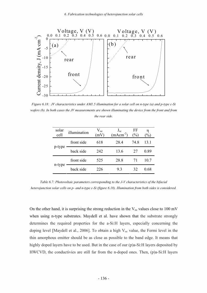
6. Fabrication technologies of heterojunction solar cells
- 136 -
Figure 6.18: JV characteristics under AM1.5 illumination for a solar cell on n-type (a) and p-type c-Si
wafers (b). In both cases the JV measurements are shown illuminating the device from the front and from
the rear side.
solar cell illumination Voc
(mV) Jsc
(mAcm-2) FF (%)
η (%)
front side 618 28.4 74.8 13.1 p-type
back side 242 13.6 27 0.89
front side 525 28.8 71 10.7 n-type
back side 226 9.3 32 0.68
Table 6.7: Photovoltaic parameters corresponding to the J-V characteristics of the bifacial
heterojunction solar cells on p- and n-type c-Si (figure 6.18). Illumination from both sides is considered.
On the other hand, it is surprising the strong reduction in the Voc values close to 100 mV
when using n-type substrates. Maydell et al. have shown that the substrate strongly
determines the required properties for the a-Si:H layers, especially concerning the
doping level [Maydell et al., 2006]. To obtain a high Voc value, the Fermi level in the
thin amorphous emitter should be as close as possible to the band edge. It means that
highly doped layers have to be used. But in the case of our (p)a-Si:H layers deposited by
HWCVD, the conductivies are still far from the n-doped ones. Then, (p)a-Si:H layers
-30
-25
-20
-15
-10
-5
00.0 0.1 0.2 0.3 0.4 0.5 0.6
(a)
rear
front
Voltage, V (V)C
urre
nt d
ensi
ty, J
(mA
·cm
-2) 0 .0 0 .1 0 .2 0 .3 0 .4 0 .5 0 .6
(b )
fron t
rear
V o ltage , V (V )
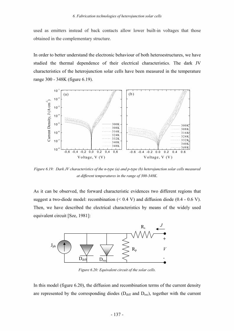
6. Fabrication technologies of heterojunction solar cells
- 137 -
used as emitters instead of back contacts allow lower built-in voltages that those
obtained in the complementary structure.
In order to better understand the electronic behaviour of both heteroestructures, we have
studied the thermal dependence of their electrical characteristics. The dark JV
characteristics of the heterojunction solar cells have been measured in the temperature
range 300 - 348K (figure 6.19).
-0 ,6 -0 ,4 -0 ,2 0,0 0,2 0,4 0,610 -8
10 -7
10 -6
1x10 -5
1x10 -4
10 -3
10 -2
10 -1
(a)
Cur
rent
Den
sity
, J (A
·cm
-2)
V oltage, V (V )
300K 308K 316K 324K 332K 340K 348K
-0 .6 -0 .4 -0 .2 0 .0 0 .2 0 .4 0 .6
(b )
V oltage , V (V )
300K 308K 316K 324K 332K 340K 348K
Figure 6.19: Dark JV characteristics of the n-type (a) and p-type (b) heterojunction solar cells measured
at different temperatures in the range of 300-348K.
As it can be observed, the forward characteristic evidences two different regions that
suggest a two-diode model: recombination (< 0.4 V) and diffusion diode (0.4 - 0.6 V).
Then, we have described the electrical characteristics by means of the widely used
equivalent circuit [Sze, 1981]:
Figure 6.20: Equivalent circuit of the solar cells.
In this model (figure 6.20), the diffusion and recombination terms of the current density
are represented by the corresponding diodes (Ddiff and Drec), together with the current
Rp
RsJ
+
-
V Jph
Drec Ddiff
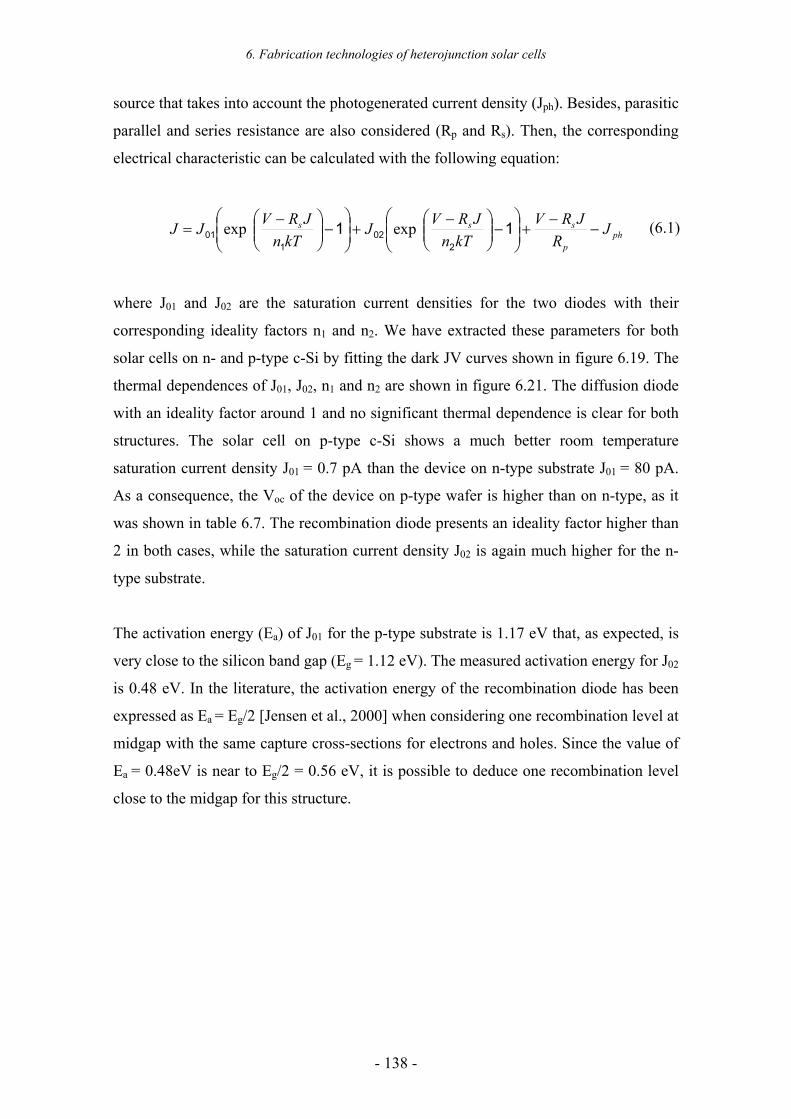
6. Fabrication technologies of heterojunction solar cells
- 138 -
source that takes into account the photogenerated current density (Jph). Besides, parasitic
parallel and series resistance are also considered (Rp and Rs). Then, the corresponding
electrical characteristic can be calculated with the following equation:
php
sss JR
JRVkTn
JRVJkTn
JRVJJ −−
+
−
−+
−
−= 11
202
101 exp exp
where J01 and J02 are the saturation current densities for the two diodes with their
corresponding ideality factors n1 and n2. We have extracted these parameters for both
solar cells on n- and p-type c-Si by fitting the dark JV curves shown in figure 6.19. The
thermal dependences of J01, J02, n1 and n2 are shown in figure 6.21. The diffusion diode
with an ideality factor around 1 and no significant thermal dependence is clear for both
structures. The solar cell on p-type c-Si shows a much better room temperature
saturation current density J01 = 0.7 pA than the device on n-type substrate J01 = 80 pA.
As a consequence, the Voc of the device on p-type wafer is higher than on n-type, as it
was shown in table 6.7. The recombination diode presents an ideality factor higher than
2 in both cases, while the saturation current density J02 is again much higher for the n-
type substrate.
The activation energy (Ea) of J01 for the p-type substrate is 1.17 eV that, as expected, is
very close to the silicon band gap (Eg = 1.12 eV). The measured activation energy for J02
is 0.48 eV. In the literature, the activation energy of the recombination diode has been
expressed as Ea = Eg/2 [Jensen et al., 2000] when considering one recombination level at
midgap with the same capture cross-sections for electrons and holes. Since the value of
Ea = 0.48eV is near to Eg/2 = 0.56 eV, it is possible to deduce one recombination level
close to the midgap for this structure.
(6.1)
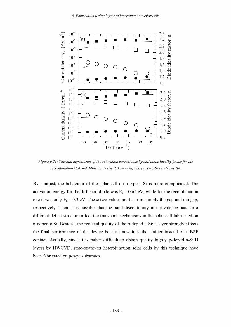
6. Fabrication technologies of heterojunction solar cells
- 139 -
1x10⁻¹⁰
1x10⁻⁹
1x10⁻⁸
1x10⁻⁷
1x10⁻⁶
1x10⁻⁵
1x10⁻⁴
(a)
Curre
nt d
ensi
ty, J
(A·c
m-2)
1,01,21,41,61,82,02,22,42,6
Dio
de id
ealit
y fa
ctor
, n
33 34 35 36 37 38 3910-1410-1310-1210-11
1x10-101x10-91x10-81x10-71x10-61x10-51x10-4
(b)
Cur
rent
den
sity,
J (A
·cm
-2)
1/kT (eV -1 )
0,81,01,21,41,61,82,02,2
Dio
de id
ealit
y fa
ctor
, n
Figure 6.21: Thermal dependence of the saturation current density and diode ideality factor for the
recombination ( ) and diffusion diodes (O) on n- (a) and p-type c-Si substrates (b).
By contrast, the behaviour of the solar cell on n-type c-Si is more complicated. The
activation energy for the diffusion diode was Ea = 0.65 eV, while for the recombination
one it was only Ea = 0.3 eV. These two values are far from simply the gap and midgap,
respectively. Then, it is possible that the band discontinuity in the valence band or a
different defect structure affect the transport mechanisms in the solar cell fabricated on
n-doped c-Si. Besides, the reduced quality of the p-doped a-Si:H layer strongly affects
the final performance of the device because now it is the emitter instead of a BSF
contact. Actually, since it is rather difficult to obtain quality highly p-doped a-Si:H
layers by HWCVD, state-of-the-art heterojunction solar cells by this technique have
been fabricated on p-type substrates.
7. Conclusions
- 140 -
Chapter 7: Conclusions
“An author is a fool who, not content with boring those he lives with, insists on boring future generations”
Montesquieu
The possibility to fabricate a-Si:H/c-Si heterojunction devices by Hot-Wire Chemical
Vapor Deposition (HWCVD) has been demonstrated in this thesis. This deposition
technique has some technological advantages compared to PECVD in terms of
deposition rate, gas decomposition and scalability. Besides, the lack of ion
bombardment could be beneficial for the interface between amorphous and crystalline
silicon. Furthermore, the a-Si:H and µc-Si:H materials obtained by HWCVD fulfill all
the optical and electrical requirements to form a good heterojunction with c-Si
substrates.
We have deeply studied the influence of the intrinsic thin buffer layer in the
heterojunction emitter. Ellipsometry measurements have been very useful to identify the
properties of the interface and the quality of the films. We have observed that the thin
intrinsic a-Si:H layer reduces the interface state density, which leads to a better surface
passivation. Besides, it also has a great influence in the growth mechanism of the n-
doped layer promoting the formation of an abrupt heterojunction. The most dense and
amorphous layers have allowed very low surface recombination velocities (Seff < 30
cm⋅s-1) and high implicit-Voc values (> 700 mV) measured by the QSSPC technique. On
the contrary, a partially epitaxial growth has been observed in heterojunction emitters
deposited directly without thin buffer layer obtaining implicit–Voc values limited to only
600 mV.
7. Conclusions
- 141 -
We have optimized the heterojunction emitter of the solar cell onto p-type wafers with a
traditional Al-BSF contact. Complete solar cells with a conversion efficiency of 15.4%
(Voc = 622 mV Jsc = 32.7 mA·cm-2, FF = 75.7%) have been fabricated. In fact, since the
implicit-Voc measured by QSS-PC was close to 700 mV for the optimized emitters, the
final Voc values of around 620 mV could be limited by the quality of the Al-BSF rear
contact. Actually, reported surface recombination velocities for Al-BSF contacts are
usually in the range of 103 cm×s-1, while we have obtained values as low as 30 cm×s-1
for a-Si:H layers.
Low temperature deposited BSF contacts based on boron-doped a-Si:H films deposited
by HWCVD have been used to replace traditional high temperature Al-BSF contacts.
Extensive experiments to optimize these low temperature BSF contacts were performed
with relatively good results. QSS-PC measurements indicate that the intrinsic buffer
layer reduces interface recombination at the back surface leading to lower Seff values.
The growth mechanism of the doped layer is also altered with the presence of the
intrinsic buffer layer, which allows a compact stack formed by an a-Si:H layer followed
by a conducting µc-Si:H one. Then, a good passivation quality (implicit-Voc > 650 mV)
can be achieved if we are able to form the desired abrupt heterojunction. Nevertheless,
the back contact is still the factor limiting the performance of our devices in terms of
Voc.
A comprehensive optimization of the front contact has been also done. On the one hand,
the ITO layer has been optimized for a high optical transmittance (> 90%) and low
electrical resistivity (< 4×10⁻⁴ Ωcm−1). State-of-the-art values have been achieved for
ITO films deposited by RF sputtering magnetron at room temperature. Nevertheless, the
control of the work function is still a subject for further research, since it has appeared
as a critical parameter to avoid parasitic Schottky barriers in the device. On the other
hand, we have also considered final technological steps such as the isolation of the solar
cell by dry-etching, the metallization process and the geometric design of the metallic
grid. Very low series resistances (< 1.5 Ωcm2) combined with high shunt resistances (>
106 Ωcm2) and low optical looses (shadowing < 6.2%) have been systematically
obtained in our heterojunction solar cells.
7. Conclusions
- 142 -
Double-side heterojunction solar cells by HWCVD with a conversion efficiency of
14.5% (Voc = 613 mV Jsc = 30.3 mA⋅cm-2, FF = 77.9%) have been fabricated in a fully
low temperature process (< 200ºC). Unfortunately, the low temperature BSF structures
with better surface passivation presented an unfavourable band configuration to contact
complete devices. Only p-doped layers with a significant crystalline fraction allowed a
good ohmic contact with the rear ITO layer. Then, the diborane flow can not be
increased too much due to its amorphization effect in HWCVD processes.
Finally, we have also started the research of heterojunction solar cells on n-type c-Si
substrates. The best structure obtained on p-type substrates was symmetrically
replicated on n-type wafers. Then, preliminary heterojunction solar cells on n-type
substrates reached promising efficiencies up to 10.7%. The JV characteristics of bifacial
solar cells on p- and n-type wafers have also been measured for illumination from the
rear side. A slight response is obtained in both cases with Voc over 200 mV, moderated
Jsc around 10 mA×cm-2 and FF around 25%.
References
- 143 -
References Aberle A.G., Crystalline Silicon Solar Cells – Advanced Surface Passivation and Analysis, Center for Photovoltaic Engineering, University of New South Wales, Sydney, (1999) Aberle A.G., Prog. Photovolt: Res. Appl. 8 (5) (2000) p.473 Alpuim P., Chu V., Conde J.P., J. Vac. Sci. Technol. A 19 (5) (2001) p.2328 Alsema E., De Wild-Scholten M., MRS Fall meeting, Boston (2005), G3.3 Altermatt P.P., Heiser G., Aberle A.G., Wang A., Zhao J., Robinson S.J., Bowden S., Green M.A., Prog. Photovolt. Res. Appl. 4, (1996) p. 399 Anderson R. L., Solid-State Electron. 5 (1962) p. 341 Antonini A., Stefancich M., Vincenzi D., Malagu C., Bici F., Ronzoni A., Martinelli G., Solar Energy Materials & Solar Cells 80 (2003) p.155 Aspnes D. E., Studna A., Kinsbron E., Phys. Rev. B 29 (1984) p. 768 Ayral A., "Techniques innovantes pour la caractérisation optique microstructurale de couches minces" , CNRS EDITIONS Bauer S., Schröder B., Oechsner H., J. Non-Cryst. Solids 227-230 (1998) p. 34 Bergmann R.B., Applied Physics A, 69, (1999) p. 187 Blakers W., Weber K. J., Everett E., Franklin E., Deenapanray P., Proc. of the 4th World Conference on Photovoltaic Energy Conversion (WCPEC '06) vol.2, Waikoloa, Hawaii, (2006) p. 2181 Boccara A. C., Fournier D., and Badoz J., Appl. Phys. Lett. 36, (1979) p. 130 Boycheva S., Krasilnikova Sytchkova A., Grilli M.L., Piegari A., Thin Solid Films 515 (2007) p. 8469 Branz H. M., Teplin C. W., Young D. L., Page M. R., Iwaniczko E., Roybal L., Bauer R., Mahan A.H., Xu Y., Stradins P., Wang T., Wang Q., Thin Solid Films, In Press, Corrected Proof (2007)
References
- 144 -
Brodsky M.H., Cardona M., Cuomo J.J., Phys. Rev. B 16, (1977) p. 3556 Brogueira P., Chu V., Ferro A.C., Conde J.P., J. Vac. Sci. Technol. A 15 (6) (1997) p.2968 Bruggemann D.A.G., Ann Phys. (Leipzig) 24 (1935) p. 636 Burgers A. R., Prog. Photovolt: Res. Appl. 7, (1999) p.457 Burgers R., Prog. Photovolt. Res. Appl. 7, (1999) p.457 Burstein E.,Phys. Rev. 93, (1954) p. 632 Bustarret E., Hachicha M.A., Brunel M., Appl. Phys. Lett. 52 (1988) p.1675 Centurioni E., Iencinella D., IEEE Electron Device Letters 24, 4 (2003) p.177 Centurioni E., Iencinella D., Rizzoli R., Zignani F., IEEE Transaction on Electron Devices 51 (11) (2004), p. 1818 Chapin D. M., Fuller C. S., Pearson G. L., J. Appl. Phys., 25 (1954) p. 676 Chen M., Pei Z.L., Wang X., Yu Y.H., Liu X.H., Sun C., Wen L.S., J. Phys. D: Appl. Phys. 33 (2000) p. 2538 Christensen J.S., Ulyashin A.G., Maknys K., Kuznetsov A.Yu. and Svensson B.G., Thin Solid Films 511 (2006) p.93 Collins R.W., Appl. Phys. Lett. 53 (12) (1988) p. 1086 Conrad E., Korte L., Maydell K. v., Angermann H., Schubert C., Stangl R., Schmidt M., Proc. Of 21st European Photovoltaic Solar Energy Conference, Dresden (2006) p.784 Cuevas A., Russell D., Prog. Photovolt. Res. Appl. 8 (2002) p. 603 Cuniot M. Lequeux N., Philosophical Magazine B, 64, 6 (1991) p.723 Curtins H., Veprek S., Solid State Communications 57 (4) (1986) p. 215 Damon-Lacoste, J., Ph.D. Thesis, Ecole Polytechnique Paris (2007) Dauwe S, Schmidt J, Hezel R. Proceedings of the 29th IEEE Photovoltaic Specialists Conference, New York, (2002) p.1246 Doyle, J., Robertson, R., Lin, G. H., He, M. Z., Gallagher, A. J.Appl. Phys. 64 (1988) p.3215 Duerinckx F. Szlufcik J., Solar Energy Materials and Solar Cells 72 ( 2002) p. 231
References
- 145 -
El Akkad F., Marafi M., Punnoose A., Prabu G., Phys. Stat. Sol. (a) 177, (2000) p. 445 Fedders P. A., Leopold D. J., Chan P. H., Borzi R., and Norberg R. E., Phys. Rev. Lett. 85 (2000) p. 401 Feenstra K. F., Schropp R. E. I., Van der Weg W. F., J.Appl. Phys. 85 (1999) p. 6843 Ferre R., Martin I., Ortega P., Vetter M., Torres I., and Alcubilla R., J. Appl. Phys. 100, (2006) p. 073703 Ferre R., Martín I., Vetter M., Garín M., and Alcubilla R., Appl. Phys. Lett. 87, (2005) p. 202109 Fesquet L., Olibet S., Vallat-Sauvain E., Shah A., Ballif C., Proc. of the 22th EU-PVSC Conference, Milan, (2007) Fonrodona M., Escarré J.,Villar F., Soler D., Asensi J.M., Bertomeu J.,Andreu J., Solar Energy Materials and Solar Cells 89 (2005) p. 37 Fonrodona M.., Ph.D. Thesis, University of Barcelona (2003) Fontcuberta i Morral A., Roca i Cabarrocas P., Clerc C., Physical Review B 69 (2004) p.125 Fontcuberta i Morral A., Roca i Cabarrocas P., Thin Solid Films 383 (2001) p. 161 Froitzheim A., Angermann H., Elstner L., Fussel W., Kliefoth K., Knechtel J., Schmidt M., Sinh N., Weiser H., Fuhs W., Proc. of the 16th European PVSEC, Glasgow (2000) p. 1580 Froitzheim A., Brendel K., Elstner L., Fuhs W., Kliefoth K., Schmidt M., J. Non-Cryst Solids 299 (2002) p.663 Fritts, C. E., American Journal of Science 26 (1883) p. 465 Fthenakis V., Alsema E., Prog. Photovolt: Res. Appl. 14 (3) (2006) p. 275 Funke C., Sciurova O., Möller H.J., Stephan M., Fröhlich K.J., Seifert C., Bachmann A., Müller A., Proc. 19th PVSEC, Paris, (2004) p.1266ç Fuhs W., Niemann K. and Stuke J., Bull. Am. Phys. Soc. 19 (1974) p. 393 Glunz S.W., Solar Energy Materials and Solar Cells 90 (2006) p.3276 Glunz S. W., Grohe A., Hofmann M., Janz S., Schultz O., Vetter M., Martín I., Ferre R., Bermejo S., Wolke W., Warta W., Preu R., and Willeke G., 20th European Photovoltaic Solar Energy Conference, Barcelona (2005) p. 572 Goetzberger A., Hebling C. Schock H.W., Mater. Sci. Eng., R 40 (2003), p. 1
References
- 146 -
Goetzberger A., Luther J., Willeke G., Solar Energy Materials & Solar Cells 74 (2002) p.1 Green M.A., Emery K., King D.L., Igari S., Warta W., Prog. Photovolt: Res. Appl. 14 (2006) p.14 Green M.A., Prog. Photovolt: Res. Appl. 14 (2006) p.383 Green M.A., Prog. Photovolt: Res. Appl. Vol. 8, 5 (2000) p.443 Green M.A, Blakers A.W., Zhao J., Milne A.M., Wang A., Dai X., IEEE Transactions on Electron Devices 37 (1990) p.331 Green M.A., Solar Cells, University of New South Wales, Sydney, Australia, (1982) p. 52 Green M.A., Solar Cells: Operating Principles, Technology and System Applications, Prentice Hall (1981) Gruenbaum PE, Gan JY, King RR, Swanson RM. Proc. of the 21st IEEE Photovoltaic Specialists Conference, Kissimimee, (1990) p. 317 Gudovskikh A.S., Ibrahim S., Kleider J.-P., Damon-Lacoste J., Roca i Cabarrocas P., Veschetti Y., Ribeyron P.-J., Thin Solid Films, In Press, Corrected Proof (2007) Guha S., Narasimhan K.L., Pietruszko S.M., J. Appl. Phys. 52 (2) (1981) p. 859 Hall R.N., Phys. Rev. 87, (1952) p. 387 Hamakawa Y., Okamoto H., Okuda K., United States Patent 4,496,788, (1985) Hamakawa Y., Thin-Film Solar Cells: Next Generation Photovoltaics and Its Applications, Springer (2004) Han D., Wang K., Owens J.M., Gedvilas L., Nelson B., Habuchi H., Tanaka M., J. Appl. Phys. 93 (7) (2003) p. 3776 Han D., Yue G., Lorentzen J.D., Lin J., Habuchi H., Wang Q., J. Appl. Phys. 87 (2000) p. 1882 Hegedus S., Prog. Photovolt: Res. Appl. 14, (2006) p.393 Heintze M., Zedlitz R., Wanka H.N., Schubert M.B., J. Appl. Phys. 79 (1996) p. 2699 Hering G., Spectrolab reports 40.7-percent cell efficiency—world record, Photon international (2007) p. 1 Hermle, M., Dicker, J.,Warta, W.,Glunz, S.W., Willeke, G. Proc. of 3rd World Conference on Photovoltaic Energy Conversion, Vol.2 (2003) p.1009
References
- 147 -
Hermle M., Schneiderlöchner E. , Grupp G., Glunz S. W., Proc. of the 20th European Photovoltaic Solar Energy Conference, Barcelona (2005) p.810 Honda N., Masuda A., Matsumura H., J. Non-Cryst. Solids 266 (2000) p.100 Horbach C., Beyer W., Wagner H., J. Non-Cryst. Solids 137 (1991) p.661 http://us.sanyo.com/industrial/solar/downloads/0619%20SANYO%20HIT%20Energy%20Conversion%20Efficiency.pdf http://www.avasolar.com/ http://www.ecn.nl/library/reports/2006/c060010.html http://www1.eere.energy.gov/solar/pv_basics.html Huster F., Proceedings of the 20th European Photovoltaic Solar Energy Conference and Exhibition, Barcelona, (2005) p. 635 Ishibashi K, Thin Solid Films 395 (2001) p. 55 Jadkar S. Jaydeep R., Sali V., Musale D. V., S. Kshirsagar T., Takwale M. G., Solar Energy Materials and Solar Cells 71 (2002) p.153 Jellison Jr. G.E. Chisholm M.F., Gorbatkin S.M., Appl. Phys. Lett. 62 (25) (1993) p. 348 Jellison Jr. G.E., Modine F.A., Appl. Phys. Lett, 69 (1996) p. 371 Jellison Jr. G.E., Thin Solid Films 234 (1994) p. 419 Jeong J.W., Rohatgi A., Yelendur V., Ebong A., Rosenblum M.D., Kalejs J.P., IEEE Transactions on Electron Devices 48 (2001) p. 2836 Jensen N., Rau U., Hausner M., Uppal S., Oberbeck L., Bergmann R.B., Werner J. H., J. of Appl. Phys., 87, 5 (2000) p.2639 Jensen, N., Hausner, R.M., Bergmann, R.B., Werner, J.H., Rau, U., Prog. Photovolt: Res. Appl., 10, (2003) p. 1 Kail F., Ph.D. Thesis, Ecole Polytechnique Paris (2005) Karasawa T. and Miyata Y., Thin Solid Films 223, (1993) p. 135 Kim J. S., Lagel B., Moons E., Johansson N., Baikie I. D., Salaneck W. R., Friend R. H., Cacialli F., Synth. Metal 111(2000) p. 311 Kim Y.S., Drowly C.I. Hu C., Conf. Record 14th IEEE Photovoltaic Specialists Conference, San Diego, (1980) p. 560
References
- 148 -
King D.L., Schubert W.K., Hund T.D., Conf. Record, 1st World Conference on Photovoltaic Energy Conversion, Hawaii, (1994) p.1660 Knapp K., Jester T. Solar Energy, 71 (3), (2001) p. 165 Kobayashi H., Ishida T., Nakato Y., Tsubomura H., J. Appl. Phys. 69 (1991) p.6065 Koh J., Ferlauto A.S., Rovira P.I., Wronski C.R., Collins R.W., Appl. Phys. Lett. 75 (1999) p. 2286 Kunst M., von Aichberger S., Citarella G., Wünsch F., J. Non-Cryst. Sol. 299 (2002) p.1198 Kunst M., Abdallah O. and Wünsch F., Sol. Energy Mater. Sol. Cells 72, 335 (2002b) Langford A.A., Fleet M.L., Nelson B.P., Lanford W.A., Maley N., Phys. Rev. B 45 (1992) p. 13367 Lauinger T., Schmidt J., Aberle A.G., Hezel R., Appl. Phys. Lett. 68 (1996) p.1232 Le Quang N. , Goaer G., Coustier F., Gauthier M., Duffar T., Delannoy Y., Mangelinck N., Barvinschi F.- Proc. of the 19th European Photovoltaic Solar Energy Conference and Exhibition (2004) p. 1259 Lee J.Y., Glunz S.W., Solar Energy Materials and Solar Cells 90 (2006) p.82 Leguijt C, Lölgen P, Eikelboom JA, Weeber AW, Schuurmans FM, Sinke WC, Alkemade PFA, Sarro PM, Marée CHM, Verhoef LA, Solar Energy Materials and Solar Cells 40, (1996) p.297
Liu F., Zhu M., Feng Y., Han Y., Liu J., Kasouit S., Vanderhaghen R., J. Non-Cryst. Sol. 299 (2002) p.385
Losurdo M., Grimaldi A., Sacchetti A., Capezzuto P., Ambrico M., Bruno G., Roca F., Thin Solid Films 427(2003) p. 171 Lucovsky G., Nemanich R.J., Knights J.C., Physical Review B 19 (4) (1979) p. 2064 Mäckel H., Lüdemann R., J Appl Phys 92 (2002), p. 2602 Mahan A. H., Carapella J., Nelson B. P., Crandall R. S., Balberg I., J.Appl. Phys. 69, (1991) p.6728 Mahan A.H., Thin Solid Films 501 (2006) p. 3 Mahan A.H., Nelson B.P., Salamon S., Crandall R.S., J. Non-Cryst Solids 137 (1991) p.657 Mahan A.H., Sol. Energy Materials & Solar Cells 78 (2003) p. 299
References
- 149 -
Mahan A.H., Yang J., Guha S., Williamson D.L., Phys. Rev. B 61 (3) (2000) p. 1677 Mahan, A. H., Carapella, J., Nelson, B. P., Crandall, R. S., J . Appl. Phys. 69, (1991) p.6728 Maissell L.I. Glang R. (eds.), Handbook of Thin film Technology, Mc Graw Hill, New York, (1970) Martín I., Vetter M., Orpella A., Puigdollers J., Cuevas A. , Alcubilla R., Appl. Phys. Lett. 79 (2001) p. 2199 Martín I., Vetter M., Orpella A., Voz, C., Puigdollers J., Alcubilla R., Kharchenko A.V., and Roca i Cabarrocas P., Appl. Phys. Lett. 84 (2004) p. 1474 Martín I., Vetter M., Garín M., Orpella A., Voz C., Puigdollers J., and Alcubilla R., J. Appl. Phys. 98, (2005) p. 114912 Martín I., Vetter M., Orpella A., Voz C., Puigdollers J., and Alcubilla R., Appl. Phys. Lett. 81, (2002) p. 4461 Martin, Ph.D. Thesis, Universitat Politècnica de Catalunya (2004) Matsumura H., Jap.J. Appl.Phys. 25 (1886) p. 1949 Maydell K. v., Conrad E., Schmidt M., 15th International Photovoltaic Science and Engineering Conference, Shanghai, (2005) p. 881 Maydell K., Conrad E., Schmidt M., Prog. Photovolt: Res. Appl. 14 (2006) p.289 Maydell, K. v., Schmidt, M., Korte, L., Laades, A., Conrad, E., Stangl, R., Scherff, M. & Fuhs, W., 31 IEEE Photovoltaic Specialists Conference held in Coronado Springs Resort, Lake Buena Vista (2005) p. 1225 Maydell K.v., Korte L., Laades A., Stangl R., Conrad E., Lange F. and Schmidt M., J. Non-Cryst. Sol. 352 (2006) p. 1958 Meng L., dos Santos M.P., Thin Solid Films 322 (1998) p.56 Minami T., J. Vac. Sci. Technol. A, 17 (1999) p. 1765 Möller H.J., Adv. Eng. Mater. 6 (2004) p. 501 Morikawa H., Fujita M., Thin Solid Films 339 (1999) p.309 Morikawa H., Fujita M., Thin Solid Films, 359 (2000) p.61 Moutinho H.R., Romero M.J., Jiang C.-S., Xu Y., Nelson B.P., Jones K.M., Mahan A.H., Al-Jassim M.M., Proc. of the 29th IEEE PV Specialists Conference, New Orleans (2002)
References
- 150 -
Muñoz D., Voz C., Martin I., Orpella A., Puigdollers J., Alcubilla R., Villar F., Bertomeu J., Andreu J., Damon-Lacoste J., Roca i Cabarrocas P., Thin Solid Films 516, (2008) p.761 Nath P., Bunshah R.F., Basol B.M., Staffsud O.M., Thin Solid Films 72 (1980) p. 463 Nelson B., Iwaniczko E., Mahan A.H., Wang Q., Xu Y. Crandall R.S., Branz H.M., Thin Solid Films 395 (2001) p.292 Niikura C., Guillet J., Brenot R., Equer B., Bouree J.E., Voz C., Peiro D., Asensi J.M., Bertomeu J., Andreu J., J. Non-Cryst. Sol. 266 (2000) p.385 Nisha M., Anusha S., Antony A., Manoj R. and Jayaraj M.K., Appl. Surf. Sci. 252 (2005) p.1430 Ohring M., The materials science of thin films, Academic Press, (1992) Olibet S., Vallat-Sauvain E., Ballif C., Physical Review B, 76, (2007) p.35326 Page M.R., Wang Q., Wang T.H., Yan Y., Johnston S.W., Ciszek T.F., Proc. Of 13th Workshop on Crystalline Silicon Solar Cell Materials and Processes, Colorado (2003) Page, M. R., Iwaniczko, E., Xu, Y., Wang, Q., Yan, Y., Roybal, L., Branz, H. M., Wang, T. H., 4th IEEE World Conference on Photovoltaic Energy Conversion, Waikoloa, (2006) p. 6 Palik E. D., Handbook of Optical Constants of Solids, Academic, New York, (1991) Peiró D., Ph.D. Thesis, University of Barcelona (1999) Peumans P., Yakimov A., Forrest S.R., J . Appl. Phys. 93 (2003) p. 3693 Plagwitz H., Nerding M., Ott N., Strunk H.P., Brendel R., Prog. Photovolt: Res. Appl. 12, (2004) p.47 Puigdollers, J., Ph .D. Thesis, University of Barcelona (1995) Radike M., Summhammer J., Prog. Photovolt: Res. Appl. 7, (1999) p.399 Ray S., Banerjee R., Basu N., Batabyal A.K. and Barua A. K., J. Appl. Phys. 54 (1983) p.3497 Roca i Cabarrocas P., Appl. Phys. Lett. 65 (13) (1994) p. 1674 Roca i Cabarrocas P., Hamma S., Sharma S.N., Viera G., Bertran E., Costa J., J. Non-Cryst. Solids 227 (1998) p. 871 Roca i Cabarrocas P., Kumar S., Drevillon B., J. Appl. Phys. 66 (7) (1989) p. 3286
References
- 151 -
Rose D., Koehler O., Kaminar N., Mulligan B., King D., IEEE 4th World Conference on Photovoltaic Energy Conversion, Waikoloa, (2006) p. 2018 Rose D., Powell R., Jayamaha U., Maltby M., Giolando D., McMaster A., Kormanyos K., Faykosh G., Dorer G., Conf. Rec. 28th IEEE Photovoltaic Spec. Conf. (2000) p.428 Staebler D.L., Wronski C.R., Appl. Phys. Lett., 31, (1977) p. 292 Scheer h., Economía solar, Estrategias para la modernidad ecológica, Círculo de Lectores-Galaxia Guttemberg. Barcelona, (2002) Schlaf R., Murata H., Kafafi Z.H., Journal of Electron Spectroscopy and Related Phenomena 120 (2001) p.149 Schmidt J. and Aberle A.G., J. Appl. Phys. 85 (7) (1999) p. 3626 Schmidt J., and M. Kerr, Sol. Energy Mater. Sol. Cells 65 (2001), p. 585 Schmidt M., Korte L., Laades A., Stangl R., Schubert Ch., Angermann H., Conrad E., Maydell K.v., Thin Solid Films 515 (2007) p.7475 Schmidt W., Woesten B., Kalejs J.P., Prog. Photovolt: Res. Appl. 10(2) (2002) p. 129 Schneidorlöchner E., Preu R., Lüdemann R., Glunz S.W., Prog. Photovolt: Res. Appl. 10 (2002) p.29 Schropp R.E.I., Franken R.H., Goldbach H.D., Houweling Z.S., Li H., Rath J.K., Schüttauf J.W.A., Stolk R.L., Verlaan V. , van der Werf C.H.M., Thin Solid Films, In Press, Corrected Proof (2007) Schropp R.E.I., Thin Solid Films 451 (2004) p. 455 Schropp R.E.I., Zeman M., Amorphous and Microcyrstalline Silicon Solar Cells: Modeling, Materials and Device Technology, Kluwer Academic Publishers (1998) Schultz O., Riepe S., Glunz S. W., Proc. 19th PVSEC, Paris (2004) p.516 Schumacher J. O., Ph D thesis, Fraunhofer-Institut für Solare Energiesysteme Freiburg, (2000) Seitz H., Bauer S., Dusane R. O., Schröder B., Thin Solid Films 395 (2001) p.120 Shockley W. and Read W.T., Phys. Rev. 87 (1952) p. 935 Sinton R., User Manual: WCT-100 Photoconductance Tool, Sinton Consulting, Boulder, CO, (1999) Sinton R.A., Cuevas, A., Appl. Phys.Lett 69 (1996) p. 2510 Soler D., Ph.D. Thesis, University of Barcelona (2004)
References
- 152 -
Song Y.J. Anderson W.A., Solar Energy Materials & Solar Cells 64, (2000) p. 241 Spear W.E., Le Comber P.G., Solid State Communications 17 (1975) p. 1193 Stangl R, Froitzheim A, Elstner L, FuhsW., Proc. of the 17th EPVSEC, Munich, (2001) p.1387 Stangl R., Froitzheim A., Schmidt M., Fuhs W., 3rd World Conference on Photovoltaic Energy Conversion, Osaka (2003) p.1005 Stocks M.J., Weber K.J., A.W. Blakers A.W., Babaei J., Everett V., Neuendorf A., Kerr M. and Verlinden P.J., 3rd World Conference on Photovoltaic Solar Energy Conversion, Osaka, Japan (2003) Stocks M.J., Weber K.J., A.W. Blakers A.W., Babaei J., Everett V., Neuendorf A., Kerr M. and Verlinden P.J., 3rd World Conference on Photovoltaic Solar Energy Conversion, Osaka, Japan (2003) p. 184 Street R.A., Hydrogenated Amorphous Silicon, Cambridge University Press, Cambridge (1991) Sugiyama K., Ishii H., Ouchi Y., Seki K., J. Appl. Phys. 87 (2000) p. 295 Swanepoel R., J. Phys. E: Sci. Instrum., vol. 16, 1983, p.1214 Swanson, R.M., 19th European Photovoltaic Solar Energy Conference, Paris, (2004) p.1078 Sze M., Physics of semiconductor devices, 2nd ed. (Wiley, New York, 1981) Sze S.M., Physics of semiconductor devices, Wiley & Sons, New York (1985) Szlufcik J., Duerinckx F., Horzel J., E. Van Kerschaver E., Dekkers H., De Wolf S., Choulat P., Allebe C., Nijs J., Solar Energy Materials and Solar Cells 74, (2002) p. 155 Tadayyon S.M., Grandin H.M., Griths K. , Coatsworth L.L., Norton P.R., Aziz H., Popovic Z.D., Organic Electronics 5 (2004) p.199 Taguchi M., Kawamoto K., Tsuge S., Baba T., Sakata H., Morizane M., Uchihashi K., Nakamura N., Kiyama S., Oota O., Prog. Photovolt: Res. Appl. 8 (2000) p. 503 Taguchi M., Tanaka M., Matsuyama T., Matsuoka T., Tsuda S., Nakano S., Kishi Y., Kuwano Y. Technical Digest of the International PVSEC-5, Kyoto, (1990) p.689 Taguchi M., Terakawa A., Maruyama E., Tanaka M., Prog. Photovolt. Res. Appl. 13 (2005) p. 481 Tanaka M., Okamoto S., Tsuge S., Kiyama S., Proc. of the 3rd World Conf. PV Energy Conv., Osaka, (2003) p.955
References
- 153 -
Tauc J., Amorphous and Liquid Semiconductors, Plenum Press, London (1974) Terzini E., Thilakan P., Minarini C., Materials Science and Engineering B77 (2000) p.110 Torres P., Meier J., Flückiger R., Kroll U., Anna Selvan J.A., Keppner H., Shah A., Appl. Phys. Lett. 69 (1996) p. 1373 Tsu D.V., Chao B.S., Ovshinsky S.R., Guha S., Yang J., Appl. Phys. Lett. 71 (10) (1997) p. 1317 Tsu R., González-Hernández J., Chao S.S., Lee S.C., Tanaka K., Appl. Phys. Lett. 40 (1982) p. 534 Tucci M., della Noce M., Bobeico E., Roca F., de Cesare G. Palma F., Thin Solid Films 451 (2004) p.355 Tucci M., Salurso E., Roca F., Palma F., Thin Solid Films 403 (2002) p. 307 Ulyashin A. G., Job R., Scherff M., Meizhen Gao, Fahrner W. R., Lyebyedyev D., Roos N. and. Scheer H., Thin Solid Films 403, (2002) p.359 Unold T., Rösch M., Bauer G.H., J. Non-Cryst. Solids 266 (2000) p.1033 Van Cleef M. W. M., Rath J. K., Rubinelli F. A., van der Werf C. H. M., Schropp R. E. I., van der Weg W. F., J . Appl. Phys 82, (1997) p. 6089 Van der Walle C.G., Neugebauer J., Applied Physics Letters 70, (1997) p. 2577 Van Hove L., Phys. Rev. 89 (1953) p. 1189 Van Veen M., Ph.D. Thesis, Utrech University (2003) Van Veenendaal P.A.T.T., Gijzeman O.L.J., Rath J.K., Schropp R.E.I., Thin Solid Films 395 (2001) p. 194 Veschetti Y., Muller J.-C., Damon-Lacoste J., Roca i Cabarrocas P., Gudovskikh A.S., Kleider J.-P., Ribeyron P.-J. , Rolland E., Thin Solid Films 511, (2006) p. 543 Veschetti, Ph.D. Thesis, Université Louis Pasteur Strasbourg 1 (2005) Villar F., Ph.D. Thesis, University of Barcelona (2008) Voz C. , Peiro D., Bertomeu J., Soler D., Fonrodona M., Andreu J., Mater. Sci. Eng. B 69/79 (2000) p.278 Voz C., Martin I., Orpella A., Puigdollers J., Vetter M., Alcubilla R., Soler D., Fonrodona M., Bertomeu J. and Andreu J., Thin Solid Films 430 (2003) p.270
References
- 154 -
Voz C., Peiró D., Bertomeu J., Soler D., Fonrodona M., Andreu J., Materials Science and Engineering B 69-70 (2000) p. 278 Voz C., Ph.D. Thesis, University of Barcelona (2000) Wald FV. In Crystals: Growth, Properties and Applications 5, Grabmaier J (ed.). Springer: Berlin, (1981) p. 147–198 Wang T.H., Iwaniczko E., Page M.R., Levi D.H., Yan Y., Branz H.M., and Wang Q., Yelundur V., Rohatgi A. Proc. of the 31st IEEE Photovoltaics Specialists Conference and Exhibition, Florida (2005) Wang T.H., Iwaniczko E., Page M.R., Levi D.H., Yan Y., Branz H.M., Wang Q. Thin Solid Films 501 (2006) p.284 Wang T.H., Page M.R., Iwaniczko E., Levi D.H., Yan Y., Branz H.M., Yelundur V., Rohatgi A., Bunea G., Terao A., Wang Q., Proc. of 14th Workshop on Crys. Silicon Solar Cells and Modules, (2004) Wang T.H., Wang Q., Iwaniczko E., Page M.R., Levi D.H., Teplin C.W., Xu Y., Wu X.Z., Branz H.M., Proceedings 19th European PVSEC (Paris) (2004), p. 1296 Wiesmann H., Gosh A.K., McMahon T., Strongin M., J. Appl. Phys. 64 (1979) p.3752 Winer K., Street R. A., Johnson N. M., Walker J., Phys. Rev. B 42, (1990) p. 3120 Yamamoto K., Nakajima A., Yoshimi M., Sawada T., Fukuda S., Suezaki T., Ichikawa M., Koi Y., Goto M., MeguroT., Matsuda T., Kondo M., Sasaki T., Tawada Y., Prog. Photovolt: Res. Appl. 13 (2005) p. 489 Zebaze Kana M.G., Centurioni E., Iencinella D. Summonte C., Thin Solid Films 500, (2006) p.203 Zedlitz R., Kessler F., Heintze M., J. Non-Cryst. Solids 164 (1993) p. 83 Zhao J, Wang A, Yun F, Zhang G, Roche DM, Wenham SR, Green MA. Progress in Photovoltaics: Research and Applications 5 (1997) p.269 Zhao J. H., Wang A. H., Green M. A., Ferrazza F., Appl. Phys. Lett. 73 (1998) p. 1991 Zhao J., Wang A., Green M.A, Prog. Photovolt: Res. Appl. 7 (6) (1999) p.471 Zhao J., Wang A., Yun F., Zhang G., Roche D.M., Wenham S.R., Green M.A., Progress Prog. Photovolt: Res. Appl. 5 (1997) p.269
List of figure captions
- 155 -
List of figure captions Figure 1.1: Territory size shows the proportion of the world population living in poverty living there (calculated by multiplying population by one of two poverty indices [http://www.worldmapper.org/]. The human poverty index uses indicators that capture non-financial elements of poverty, such as life expectancy, adult literacy, water quality, and children that are underweight. [http://hdr.undp.org]). Figure 1.2: Territory size shows the proportion of all people with some electrical power in their homes living there [http://www.worldmapper.org/]. Electricity access includes that sourced from a publicly used grid and self-generated electricity. This map shows access, not the quantities of electricity used. The percentage of people with access to electricity in their own homes is over 97% in Eastern Asia, Eastern Europe, North America, Western Europe and Japan. 7 of the 10 territories with the lowest access to electricity are in Africa. Figure 1.3: Amount of solar energy in hours, received each day on an optimally tilted surface during the worst month of the year.
Figure 1.4: First solar cells and modules by Bell laboratories. Figure 1.5: PERL (passivated emitter, rear locally-diffused) solar cell structure fabricated by the group of M. Green at University of New South Wales [Zhao et al., 1999]. Figure 1.6: Very thin solar cell (20.2% on 37 µm) fabricated at ISE. They have also the record 21.2% on a 75 µm wafer without wafer warpage [Glunz et al., 2005]. Figure 1.7: Structure of the bifacial heterojunction solar cells fabricated by Sanyo. Figure 1.8: Scheme of the fabrication steps for a conventional solar cell compared to an heterojunction device. The temperatures involved in the different fabrication steps are indicated [Roca et al., 2004]. Figure 2.1: Diagram of the fabrication steps followed to obtain the complete solar cell. Figure 2.2: CZ and FZ processes for the production of monocrystalline silicon ingots.
Figure 2.3: band diagram of n-type (a) and p-type (b) bifacial heterojunction devices [Wang et al., 2004].
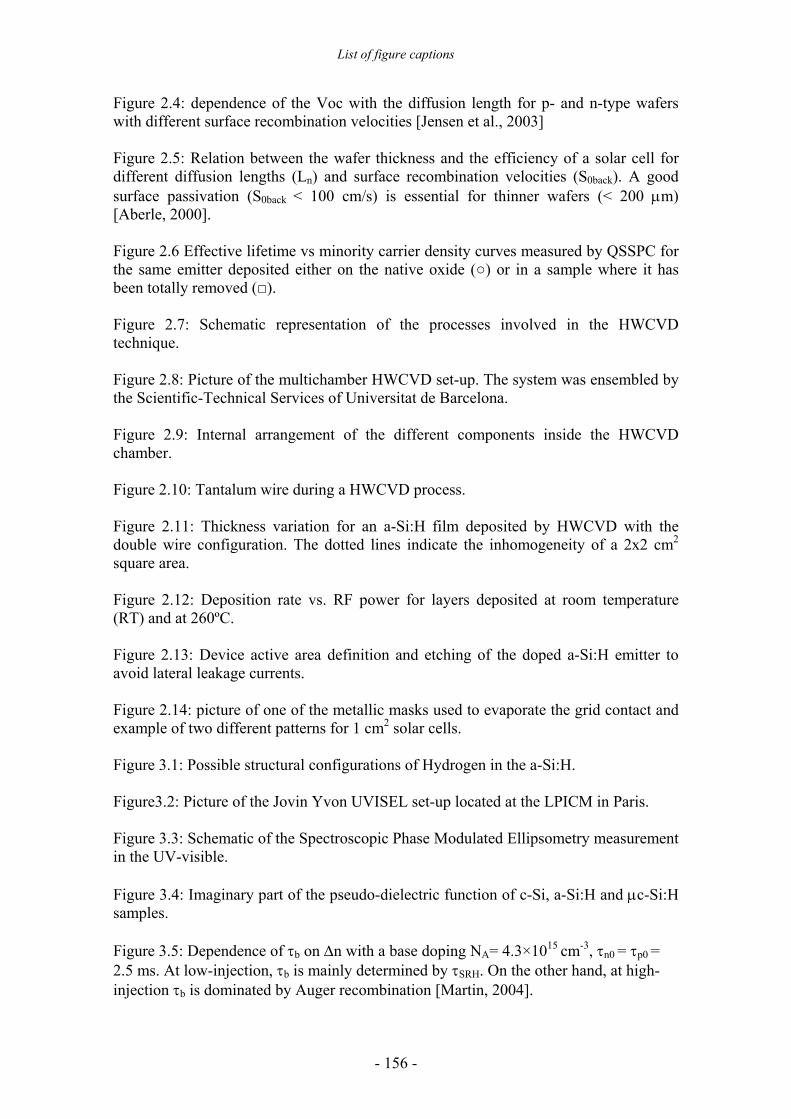
List of figure captions
- 156 -
Figure 2.4: dependence of the Voc with the diffusion length for p- and n-type wafers with different surface recombination velocities [Jensen et al., 2003] Figure 2.5: Relation between the wafer thickness and the efficiency of a solar cell for different diffusion lengths (Ln) and surface recombination velocities (S0back). A good surface passivation (S0back < 100 cm/s) is essential for thinner wafers (< 200 µm) [Aberle, 2000].
Figure 2.6 Effective lifetime vs minority carrier density curves measured by QSSPC for the same emitter deposited either on the native oxide () or in a sample where it has been totally removed ().
Figure 2.7: Schematic representation of the processes involved in the HWCVD technique. Figure 2.8: Picture of the multichamber HWCVD set-up. The system was ensembled by the Scientific-Technical Services of Universitat de Barcelona. Figure 2.9: Internal arrangement of the different components inside the HWCVD chamber. Figure 2.10: Tantalum wire during a HWCVD process. Figure 2.11: Thickness variation for an a-Si:H film deposited by HWCVD with the double wire configuration. The dotted lines indicate the inhomogeneity of a 2x2 cm2 square area. Figure 2.12: Deposition rate vs. RF power for layers deposited at room temperature (RT) and at 260ºC. Figure 2.13: Device active area definition and etching of the doped a-Si:H emitter to avoid lateral leakage currents. Figure 2.14: picture of one of the metallic masks used to evaporate the grid contact and example of two different patterns for 1 cm2 solar cells. Figure 3.1: Possible structural configurations of Hydrogen in the a-Si:H. Figure3.2: Picture of the Jovin Yvon UVISEL set-up located at the LPICM in Paris.
Figure 3.3: Schematic of the Spectroscopic Phase Modulated Ellipsometry measurement in the UV-visible. Figure 3.4: Imaginary part of the pseudo-dielectric function of c-Si, a-Si:H and µc-Si:H samples.
Figure 3.5: Dependence of τb on ∆n with a base doping NA= 4.3×1015 cm-3, τn0 = τp0 = 2.5 ms. At low-injection, τb is mainly determined by τSRH. On the other hand, at high-injection τb is dominated by Auger recombination [Martin, 2004].
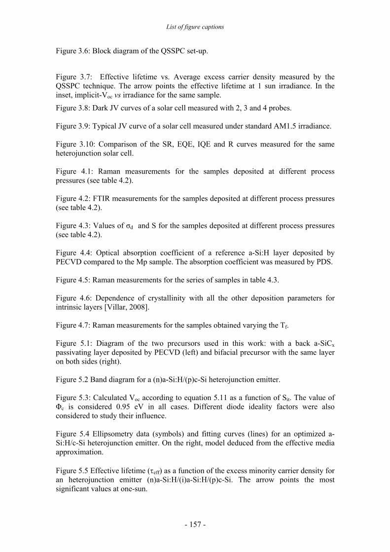
List of figure captions
- 157 -
Figure 3.6: Block diagram of the QSSPC set-up.
Figure 3.7: Effective lifetime vs. Average excess carrier density measured by the QSSPC technique. The arrow points the effective lifetime at 1 sun irradiance. In the inset, implicit-Voc vs irradiance for the same sample.
Figure 3.8: Dark JV curves of a solar cell measured with 2, 3 and 4 probes. Figure 3.9: Typical JV curve of a solar cell measured under standard AM1.5 irradiance. Figure 3.10: Comparison of the SR, EQE, IQE and R curves measured for the same heterojunction solar cell. Figure 4.1: Raman measurements for the samples deposited at different process pressures (see table 4.2). Figure 4.2: FTIR measurements for the samples deposited at different process pressures (see table 4.2). Figure 4.3: Values of σd and S for the samples deposited at different process pressures (see table 4.2). Figure 4.4: Optical absorption coefficient of a reference a-Si:H layer deposited by PECVD compared to the Mp sample. The absorption coefficient was measured by PDS. Figure 4.5: Raman measurements for the series of samples in table 4.3. Figure 4.6: Dependence of crystallinity with all the other deposition parameters for intrinsic layers [Villar, 2008]. Figure 4.7: Raman measurements for the samples obtained varying the Tf. Figure 5.1: Diagram of the two precursors used in this work: with a back a-SiCx passivating layer deposited by PECVD (left) and bifacial precursor with the same layer on both sides (right). Figure 5.2 Band diagram for a (n)a-Si:H/(p)c-Si heterojunction emitter. Figure 5.3: Calculated Voc according to equation 5.11 as a function of Sit. The value of Φc is considered 0.95 eV in all cases. Different diode ideality factors were also considered to study their influence. Figure 5.4 Ellipsometry data (symbols) and fitting curves (lines) for an optimized a-Si:H/c-Si heterojunction emitter. On the right, model deduced from the effective media approximation. Figure 5.5 Effective lifetime (τeff) as a function of the excess minority carrier density for an heterojunction emitter (n)a-Si:H/(i)a-Si:H/(p)c-Si. The arrow points the most significant values at one-sun.
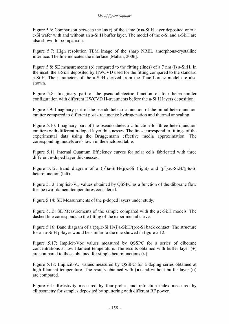
List of figure captions
- 158 -
Figure 5.6: Comparison between the Im(ε) of the same (n)a-Si:H layer deposited onto a c-Si wafer with and without an a-Si:H buffer layer. The model of the c-Si and a-Si:H are also shown for comparison. Figure 5.7: High resolution TEM image of the sharp NREL amorphous/crystalline interface. The line indicates the interface [Mahan, 2006]. Figure 5.8: SE measurements (o) compared to the fitting (lines) of a 7 nm (i) a-Si:H. In the inset, the a-Si:H deposited by HWCVD used for the fitting compared to the standard a-Si:H. The parameters of the a-Si:H derived from the Tauc-Lorenz model are also shown. Figure 5.8: Imaginary part of the pseudodielectric function of four heteroemitter configuration with different HWCVD H-treatments before the a-Si:H layers deposition. Figure 5.9: Imaginary part of the pseudodielectric function of the initial heterojunction emitter compared to different post -treatments: hydrogenation and thermal annealing. Figure 5.10: Imaginary part of the pseudo dielectric function for three heterojunction emitters with different n-doped layer thicknesses. The lines correspond to fittings of the experimental data using the Bruggemann effective media approximation. The corresponding models are shown in the enclosed table. Figure 5.11 Internal Quantum Efficiency curves for solar cells fabricated with three different n-doped layer thicknesses. Figure 5.12: Band diagram of a (p+)a-Si:H/(p)c-Si (right) and (p+)µc-Si:H/(p)c-Si heterojunction (left). Figure 5.13: Implicit-Voc values obtained by QSSPC as a function of the diborane flow for the two filament temperatures considered. Figure 5.14: SE Measurements of the p-doped layers under study. Figure 5.15: SE Measurements of the sample compared with the µc-Si:H models. The dashed line corresponds to the fitting of the experimental curve. Figure 5.16: Band diagram of a (p)µc-Si:H/(i)a-Si:H/(p)c-Si back contact. The structure for an a-Si:H p-layer would be similar to the one showed in figure 5.12. Figure 5.17: Implicit-Voc values measured by QSSPC for a series of diborane concentrations at low filament temperature. The results obtained with buffer layer () are compared to those obtained for simple heterojunctions (). Figure 5.18: Implicit-Voc values measured by QSSPC for a doping series obtained at high filament temperature. The results obtained with () and without buffer layer () are compared. Figure 6.1: Resistivity measured by four-probes and refraction index measured by ellipsometry for samples deposited by sputtering with different RF power.
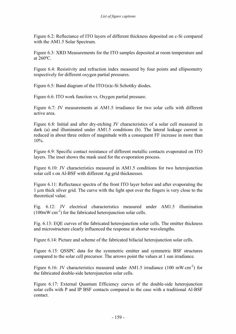
List of figure captions
- 159 -
Figure 6.2: Reflectance of ITO layers of different thickness deposited on c-Si compared with the AM1.5 Solar Spectrum. Figure 6.3: XRD Measurements for the ITO samples deposited at room temperature and at 260ºC. Figure 6.4: Resistivity and refraction index measured by four points and ellipsometry respectively for different oxygen partial pressures.
Figure 6.5: Band diagram of the ITO/(n)c-Si Schottky diodes.
Figure 6.6: ITO work function vs. Oxygen partial pressure.
Figure 6.7: JV measurements at AM1.5 irradiance for two solar cells with different active area. Figure 6.8: Initial and after dry-etching JV characteristics of a solar cell measured in dark (a) and illuminated under AM1.5 conditions (b). The lateral leakage current is reduced in about three orders of magnitude with a consequent FF increase in more than 10%. Figure 6.9: Specific contact resistance of different metallic contacts evaporated on ITO layers. The inset shows the mask used for the evaporation process.
Figure 6.10: JV characteristics measured in AM1.5 conditions for two heterojunction solar cell s on Al-BSF with different Ag grid thicknesses. Figure 6.11: Reflectance spectra of the front ITO layer before and after evaporating the 1 µm thick silver grid. The curve with the light spot over the fingers is very close to the theoretical value. Fig. 6.12: JV electrical characteristics measured under AM1.5 illumination (100mW⋅cm-2) for the fabricated heterojunction solar cells. Fig. 6.13: EQE curves of the fabricated heterojunction solar cells. The emitter thickness and microstructure clearly influenced the response at shorter wavelengths. Figure 6.14: Picture and scheme of the fabricated bifacial heterojunction solar cells. Figure 6.15: QSSPC data for the symmetric emitter and symmetric BSF structures compared to the solar cell precursor. The arrows point the values at 1 sun irradiance. Figure 6.16: JV characteristics measured under AM1.5 irradiance (100 mW⋅cm-2) for the fabricated double-side heterojunction solar cells. Figure 6.17: External Quantum Efficiency curves of the double-side heterojunction solar cells with P and IP BSF contacts compared to the case with a traditional Al-BSF contact.
List of figure captions
- 160 -
Figure 6.18: JV characteristics under AM1.5 illumination for a solar cell on n-type (a) and p-type c-Si wafers (b). In both cases the JV measurements are shown illuminating the device from the front and from the rear side. Figure 6.19: Dark JV characteristics of the n-type (a) and p-type (b) heterojunction solar cells measured at different temperatures in the range of 300 - 348K. Figure 6.20: Equivalent circuit of the solar cells. Figure 6.21: Thermal dependence of the saturation current density and diode ideality factor for the recombination ( ) and diffusion diodes (O) on n- (a) and p-type c-Si substrates (b).
List of table captions
- 161 -
List of Table Captions Table 1.1: World Renewable energy consumption in 2002 and prediction for 2030 in a standard scenario [WEO, 2004]. Table 1.2: Summary of the best results obtained to date on bifacial heterojunction solar cells Table 2.1: Parameters of the two different wire configurations used in this work. Table 3.1: Summary of AM1.5 conditions. Table 4.1 Definitions of various morphologies of silicon thin films. Table 4.2: Deposition conditions studied for the intrinsic layers. The temperature of the tantalum wire is 1650ºC in all cases. Table 4.3: Deposition conditions and conductivities for the n-doped layers. The tantalum wire temperature was 1650ºC in all cases. Table 5.1 Deposition conditions of the optimized films used in the heterojunction emitters. The wire temperature is 1600ºC in all cases. Table 5.2: Different intrinsic a-Si:H thin layers used in the heterojunction emitter and passivation quality measured by QSSPC. The 20 nm n-doped layer was the same in all cases with the deposition parameters in table 5.1. Table 5.3: QSSPC and SE results obtained from the four samples with different H-treatment times. Table 5.4: QSSPC and SE results obtained for the three samples under study. Table 5.5: Deposition parameters of the p-doped a-Si:H films. We have considered separately two wire temperatures. Table 5.6: Effective media models deduced from ellipsometry measurements for all the samples shown in figure 5.13. Table 5.7: Deposition conditions for the p-doped layers under study. Table 5.8: Fittings from the ellipsometry measurements for all the samples plotted in 5.14.
List of table captions
- 162 -
Table 5.9: Deposition conditions for a film grown with a high H-dilution. Table 5.10: Fitting of the sample PH following the standard model. Table 5.11: Effective media models for the first and last samples (least and most doped, respectively) of the doping series in figure 5.17. Table 5.12: Effective media models deduced from SE measurements for the structures obtained with a diborane flow of 1sccm. Table 6.1: Summary of electrical and optical properties of ITO. The two samples
studied were deposited at room temperature and at 260ºC. The measurement methods
are: (i) four points, (ii) ellipsometry, (iii) Hall, (iv) transmittance. Layers´ thicknesses:
80 nm, except for the transmittance measurements (500nm).
Table 6.2: Parameters of the dry-etching process used to isolate the fabricated solar cells. The etching gas CF4 is diluted into O2 (20%). Table 6.3: Summary of the resistive losses of solar cells fabricated using Al-BSF contacts. We have neglected the Rs contribution due to the ITO/a-Si:H and Al-BSF contacts. Table 6.4: Photovoltaic parameters of the J-V curves measured under AM1.5 irradiance for the fabricated heterojunction solar cells. Table 6.5: Deposition conditions used to grow the silicon films of the bifacial heterojunction solar cells. The wire temperature was 1600ºC for intrinsic a-Si:H and n-doped films, but 1750 ºC for p-doped films. The doping precursors were phosphine and diborane for n- and p-type films, respectively. Table 6.6: Electrical parameters of the JV curves measured under AM1.5 irradiance for the heterojunction solar cells fabricated with the different low temperature BSF contacts. Table 6.7: Photovoltaic parameters corresponding to the J-V characteristics of the bifacial heterojunction solar cells on p- and n-type c-Si (figure 6.18). Illumination from both sides is considered.
Summary in Spanish
- 163 -
Summary in Spanish El elevado coste de producción de los módulos de silicio cristalino (c-Si) de alta
eficiencia dificulta el progreso de la industria fotovoltaica como una alternativa viable
para la producción de energía limpia. Por esta razón, los fabricantes de células solares
buscan diferentes alternativas para conseguir la deseada reducción de costes. Por
ejemplo, considerando que las obleas de c-Si representan aproximadamente el 30 - 50 %
en el precio del módulo, una opción es reducir el grosor de las obleas (< 200 µm) para
obtener así más obleas por lingote. Sin embargo, si se reduce el grosor del sustrato es
indispensable reducir también la recombinación superficial puesto que ésta es crítica
para mantener altas eficiencias en los dispositivos. Aunque la superficie del c-Si puede
pasivarse eficientemente mediante una oxidación térmica, las obleas delgadas tiendan a
doblarse en estos procesos de alta temperatura (~ 1000°C). Por otra parte, el silicio
multicristalino de bajo coste tampoco es compatible con pasos a alta temperatura debido
a la fuerte degradación del tiempo de vida en el volumen. Por este motivo, métodos
alternativos de pasivación a baja temperatura han ganado un especial interés debido a su
compatibilidad tanto con sustratos delgados como con obleas de baja calidad o bajo
coste.
Más concretamente, las células solares de heterounión en que se utilizan capas de silicio
amorfo (a-Si:H) depositadas a baja temperatura sobre obleas de c-Si han ganado interés
en la comunidad fotovoltaica debido a su alta eficiencia y rentabilidad. Sanyo ha
conseguido eficiencias de más del 19% en módulos producidos industrialmente con la
estructura denominada HIT (heterounión con capa intrínseca delgada). La novedad de
este dispositivo es la introducción de una capa de silicio amorfo intrínseco muy delgada
(5 nm) entre el c-Si y la capa dopada. Esta capa reduce drásticamente la velocidad de
recombinación en la interfaz consiguiéndose así tensiones de circuito abierto por encima
de 700 mV. La mayoría de grupos, incluido Sanyo, usan el depósito químico en fase
Summary in Spanish
- 164 -
vapor asistido por plasma de radiofrecuencia (PECVD) para obtener el silicio amorfo.
Recientemente, la técnica de depósito asistida por filamento caliente (HWCVD)
también ha demostrado un gran potencial para fabricar células de heterounión de alta
eficiencia. En la técnica HWCVD, además de algunas ventajas tecnológicas, la ausencia
de bombardeo iónico reduce el daño en la superficie del c-Si mejorando así las
propiedades en la interfaz.
En este trabajo, hemos concentrado nuestro esfuerzo en la optimización de todos los
pasos de fabricación para obtener células solares de heterounión obtenidas por HWCVD
en un proceso completamente desarrollado a baja temperatura (200ºC). Primero, hemos
optimizado el material obtenido por HWCVD variando los diferentes parámetros de
depósito (presión, temperatura de filamento, flujos de hidrógeno y silano, nivel de
dopaje, temperatura de sustrato) para obtener silicio amorfo y microcristalino de buena
calidad. Se han conseguido buenas propiedades estructurales, eléctricas y ópticas tanto
para material intrínseco como en capas dopadas.
Posteriormente, hemos optimizado el emisor de heterounión sobre sustratos tipo p de c-
Si. En particular, se ha estudiado en profundidad la influencia de la capa intrínseca de a-
Si:H así como de diferentes pretratamientos de hidrógeno en la superficie del c-Si. Se
han realizado tanto estudios de microestructura con Espectroscopía por Elipsometría
Óptica, como medidas de pasivación mediante Fotoconductancia en Estado
Cuasiestacionario. Estos estudios han permitido optimizar los precursores de células
solares hasta obtener tensiones implícitas de circuito abierto por encima de 690 mV. A
continuación se ha desarrollado el electrodo frontal atendiendo a los requerimientos
ópticos y eléctricos. Por una parte, se ha optimizado la capa antirreflectante (Oxido de
Indio dopado con Estaño) en términos de resistividad (ρ < 4×10⁻⁴Ωcm) y de
reflectancia. Luego se ha diseñado el peine metálico frontal intentando obtener un buen
compromiso entre resistencia serie y factor de sombra. Una vez optimizado todo por
separado, se han podido fabricar células solares completas con una eficiencia de
conversión de hasta el 15.4% sobre obleas de silicio CZ tipo p planas (14 Ωcm). En
estos dispositivos se ha utilizado un contacto posterior de aluminio recocido a alta
temperatura (Al-BSF).
Finalmente, hemos investigando la posibilidad de incorporar contactos posteriores
depositados a baja temperatura basados en capas de silicio amorfo dopadas con boro
Summary in Spanish
- 165 -
obtenidas por HWCVD. Estas capas se utilizarían para sustituir los contactos
tradicionales de Al-BSF a alta temperatura. Igual que se hizo para el emisor, hemos
estudiado también la influencia de los diferentes parámetros de depósito así como el
efecto de intercalar una capa intrínseca delgada. Hasta el momento, las células solares
con doble heterounión fabricadas completamente por HWCVD han alcanzado una
eficiencia de conversión del 14.5% en un proceso completo a baja temperatura (<
200ºC). Considerando el carácter preliminar de estos dispositivos, éste es un punto de
partida realmente prometedor para células solares de heterounión bifaciales fabricadas
por HWCVD.