Embed Size (px)
Citation preview

Area Efficient D/A Converters For Accurate DC Operation
by
Brandon Royce Greenley
A THESIS
submitted to
Oregon State University
in partial fulfillment ofthe requirements for the
degree of
Master of Science
Presented May 31, 2001Commencement June 2002

ACKNOWLEDGMENT
This thesis acknowledges the following people for their support and assistance:
Un-Ku Moon
Gabor Temes
Raymond Veith
Jack Hurt
Dave McKinney
Ryan Larson
John Bennett
Dong-Young Chang
Arun Rao
Peter Kiss
Craig Larson
Jenine Firth
My Parents

TABLE OF CONTENTS
Page
1. INTRODUCTION . . . . . . . . . . . . . . . . . . . . . . . . . . . . . . . . . . . . . . . . . . . . . . . . . . . . 1
1.1 Motivation . . . . . . . . . . . . . . . . . . . . . . . . . . . . . . . . . . . . . . . . . . . . . . . . . . . . . . . 1
1.2 Existing DAC Designs . . . . . . . . . . . . . . . . . . . . . . . . . . . . . . . . . . . . . . . . . . . . 2
1.3 Research Objective . . . . . . . . . . . . . . . . . . . . . . . . . . . . . . . . . . . . . . . . . . . . . . . 4
2. BASIC CONCEPTS AND FIGURES OF MERIT FOR DACS . . . . . . . . . 5
2.1 Static Performance Measures . . . . . . . . . . . . . . . . . . . . . . . . . . . . . . . . . . . . . 5
2.2 Dynamic Performance Measures . . . . . . . . . . . . . . . . . . . . . . . . . . . . . . . . . . 8
3. DAC DESIGN . . . . . . . . . . . . . . . . . . . . . . . . . . . . . . . . . . . . . . . . . . . . . . . . . . . . . . . . 10
3.1 Architecture Design . . . . . . . . . . . . . . . . . . . . . . . . . . . . . . . . . . . . . . . . . . . . . . 10
3.2 Mismatch Modeling for Architectural Optimization . . . . . . . . . . . . . . . . 12
3.2.1 Resistor vs. No-Resistor Designs . . . . . . . . . . . . . . . . . . . . . . . . . . . 173.2.2 Device Trade-Off Analysis. . . . . . . . . . . . . . . . . . . . . . . . . . . . . . . . . . 193.2.3 Switch and Device Sizing . . . . . . . . . . . . . . . . . . . . . . . . . . . . . . . . . . 20
3.3 Linear Output Current Mirror . . . . . . . . . . . . . . . . . . . . . . . . . . . . . . . . . . . . 22
3.4 Digital Circuit Design . . . . . . . . . . . . . . . . . . . . . . . . . . . . . . . . . . . . . . . . . . . . 23
3.5 Simulation Results . . . . . . . . . . . . . . . . . . . . . . . . . . . . . . . . . . . . . . . . . . . . . . . 25
4. ULTRA HIGH GAIN OP-AMP DESIGN . . . . . . . . . . . . . . . . . . . . . . . . . . . . . . 28
4.1 Op-Amp Basics . . . . . . . . . . . . . . . . . . . . . . . . . . . . . . . . . . . . . . . . . . . . . . . . . . 28
4.2 Architecture Design . . . . . . . . . . . . . . . . . . . . . . . . . . . . . . . . . . . . . . . . . . . . . . 31
4.3 MATLAB Modeling of Feed-Forward Compensation . . . . . . . . . . . . . . . 35
4.4 Simulation Results . . . . . . . . . . . . . . . . . . . . . . . . . . . . . . . . . . . . . . . . . . . . . . . 38
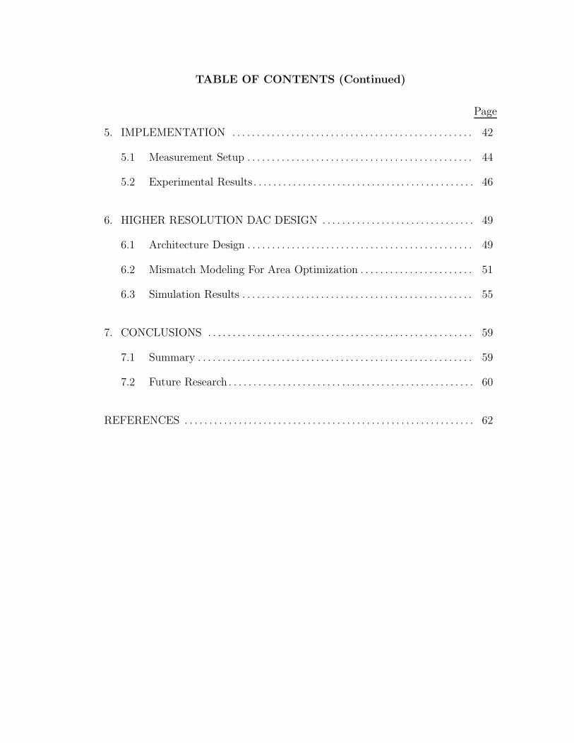
TABLE OF CONTENTS (Continued)
Page
5. IMPLEMENTATION . . . . . . . . . . . . . . . . . . . . . . . . . . . . . . . . . . . . . . . . . . . . . . . . . 42
5.1 Measurement Setup . . . . . . . . . . . . . . . . . . . . . . . . . . . . . . . . . . . . . . . . . . . . . . 44
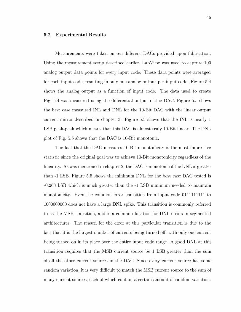
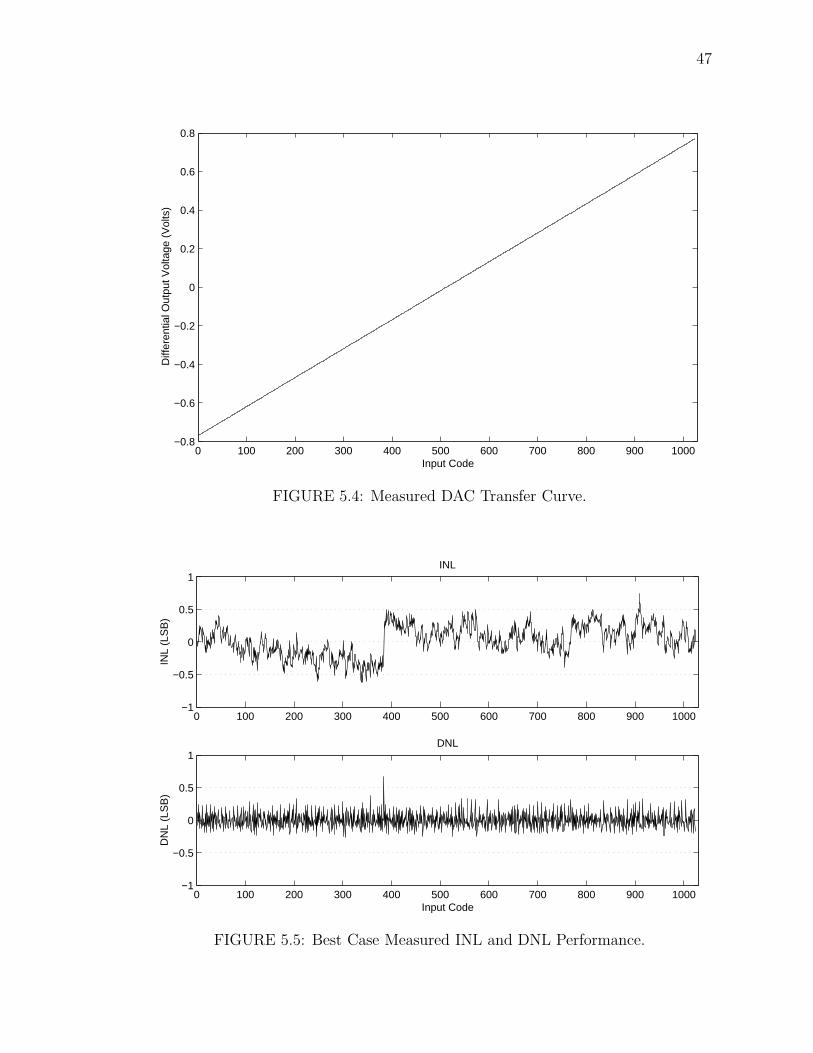
5.2 Experimental Results . . . . . . . . . . . . . . . . . . . . . . . . . . . . . . . . . . . . . . . . . . . . . 46
6. HIGHER RESOLUTION DAC DESIGN . . . . . . . . . . . . . . . . . . . . . . . . . . . . . . . 49
6.1 Architecture Design . . . . . . . . . . . . . . . . . . . . . . . . . . . . . . . . . . . . . . . . . . . . . . 49
6.2 Mismatch Modeling For Area Optimization . . . . . . . . . . . . . . . . . . . . . . . 51
6.3 Simulation Results . . . . . . . . . . . . . . . . . . . . . . . . . . . . . . . . . . . . . . . . . . . . . . . 55
7. CONCLUSIONS . . . . . . . . . . . . . . . . . . . . . . . . . . . . . . . . . . . . . . . . . . . . . . . . . . . . . . 59
7.1 Summary . . . . . . . . . . . . . . . . . . . . . . . . . . . . . . . . . . . . . . . . . . . . . . . . . . . . . . . . 59
7.2 Future Research . . . . . . . . . . . . . . . . . . . . . . . . . . . . . . . . . . . . . . . . . . . . . . . . . . 60
REFERENCES . . . . . . . . . . . . . . . . . . . . . . . . . . . . . . . . . . . . . . . . . . . . . . . . . . . . . . . . . . . 62
LIST OF FIGURES
Figure Page
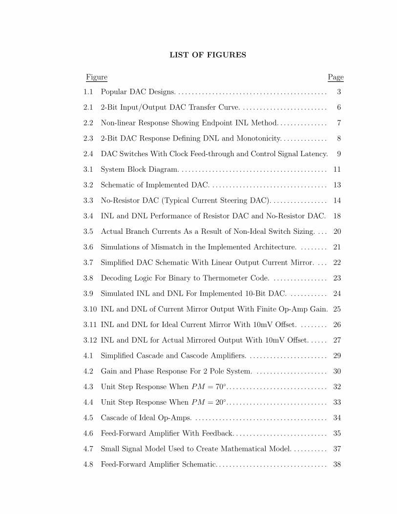
1.1 Popular DAC Designs. . . . . . . . . . . . . . . . . . . . . . . . . . . . . . . . . . . . . . . . . . . . . 3
2.1 2-Bit Input/Output DAC Transfer Curve. . . . . . . . . . . . . . . . . . . . . . . . . . 6
2.2 Non-linear Response Showing Endpoint INL Method. . . . . . . . . . . . . . . 7
2.3 2-Bit DAC Response Defining DNL and Monotonicity. . . . . . . . . . . . . . 8
2.4 DAC Switches With Clock Feed-through and Control Signal Latency. 9
3.1 System Block Diagram. . . . . . . . . . . . . . . . . . . . . . . . . . . . . . . . . . . . . . . . . . . . 11
3.2 Schematic of Implemented DAC. . . . . . . . . . . . . . . . . . . . . . . . . . . . . . . . . . . 13
3.3 No-Resistor DAC (Typical Current Steering DAC). . . . . . . . . . . . . . . . . 14
3.4 INL and DNL Performance of Resistor DAC and No-Resistor DAC. 18
3.5 Actual Branch Currents As a Result of Non-Ideal Switch Sizing. . . . 20
3.6 Simulations of Mismatch in the Implemented Architecture. . . . . . . . . 21
3.7 Simplified DAC Schematic With Linear Output Current Mirror. . . . 22
3.8 Decoding Logic For Binary to Thermometer Code. . . . . . . . . . . . . . . . . 23
3.9 Simulated INL and DNL For Implemented 10-Bit DAC. . . . . . . . . . . . 24
3.10 INL and DNL of Current Mirror Output With Finite Op-Amp Gain. 25
3.11 INL and DNL for Ideal Current Mirror With 10mV Offset. . . . . . . . . 26
3.12 INL and DNL for Actual Mirrored Output With 10mV Offset. . . . . . 27
4.1 Simplified Cascade and Cascode Amplifiers. . . . . . . . . . . . . . . . . . . . . . . . 29
4.2 Gain and Phase Response For 2 Pole System. . . . . . . . . . . . . . . . . . . . . . 30
4.3 Unit Step Response When PM = 70◦. . . . . . . . . . . . . . . . . . . . . . . . . . . . . . 32
4.4 Unit Step Response When PM = 20◦. . . . . . . . . . . . . . . . . . . . . . . . . . . . . . 33
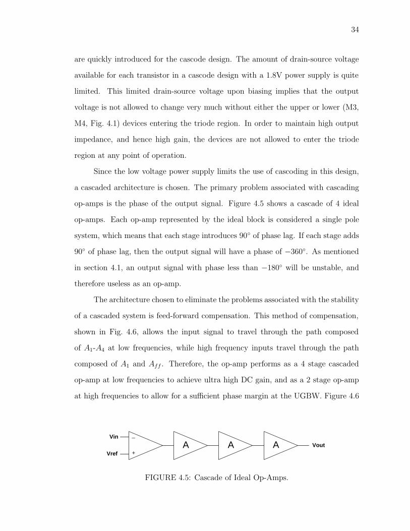
4.5 Cascade of Ideal Op-Amps. . . . . . . . . . . . . . . . . . . . . . . . . . . . . . . . . . . . . . . . 34
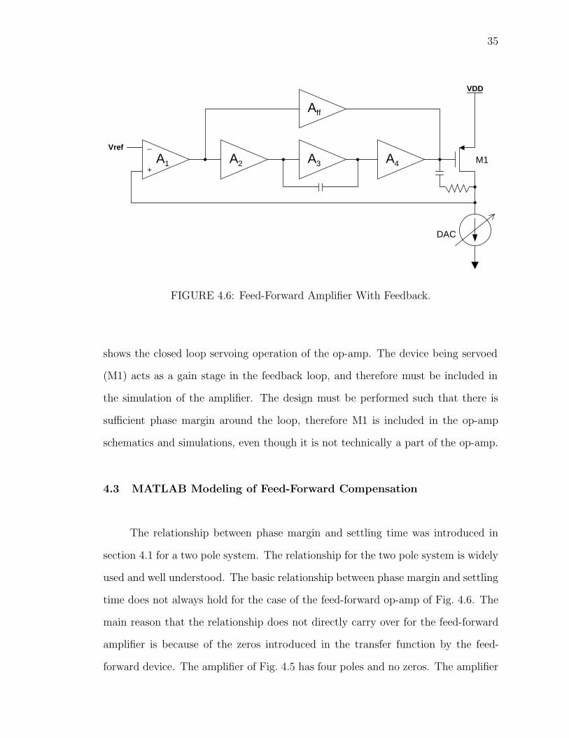
4.6 Feed-Forward Amplifier With Feedback. . . . . . . . . . . . . . . . . . . . . . . . . . . . 35
4.7 Small Signal Model Used to Create Mathematical Model. . . . . . . . . . . 37
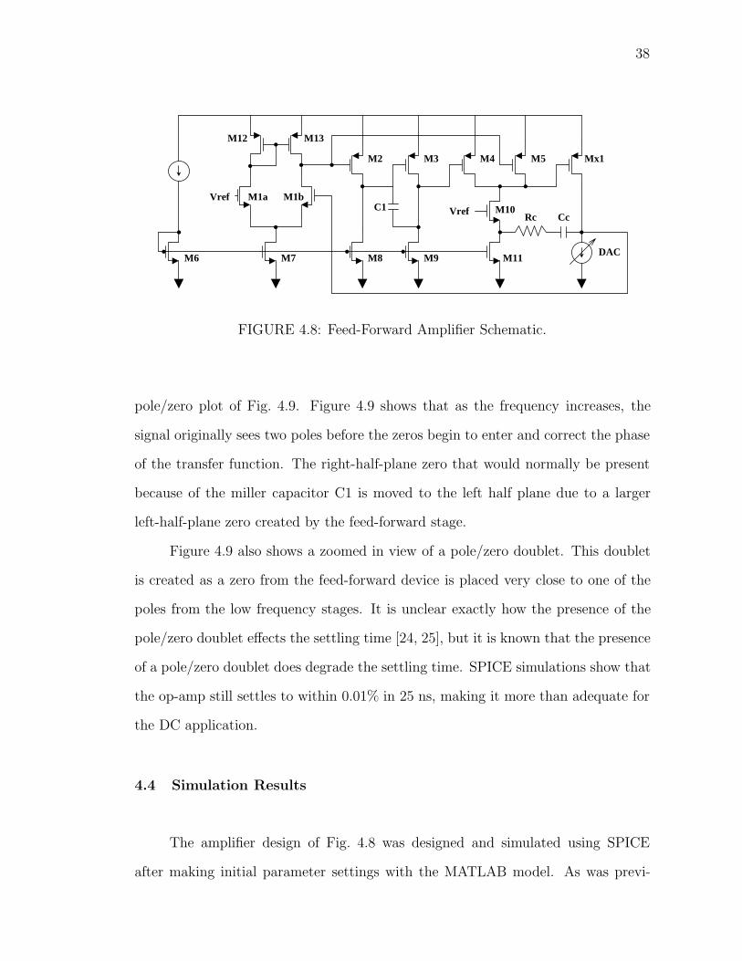
4.8 Feed-Forward Amplifier Schematic. . . . . . . . . . . . . . . . . . . . . . . . . . . . . . . . . 38
LIST OF FIGURES (Continued)
Figure Page
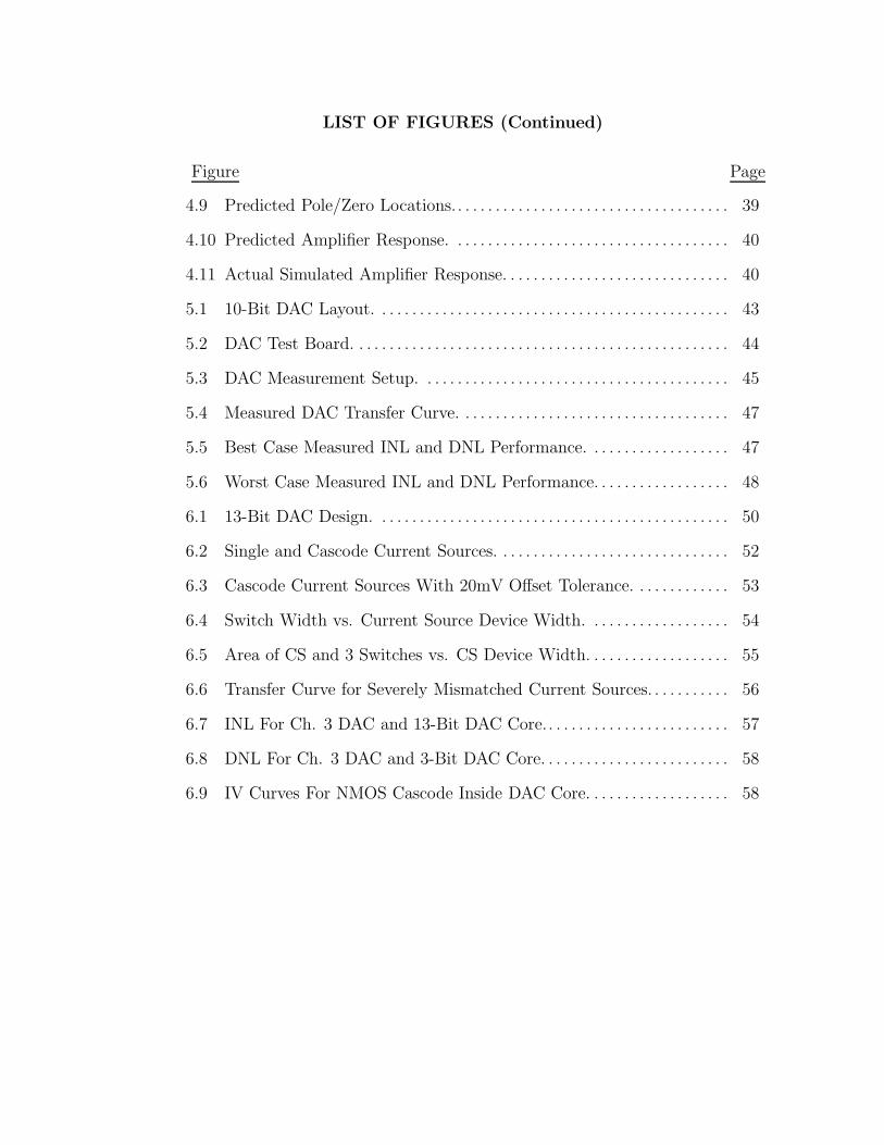
4.9 Predicted Pole/Zero Locations.. . . . . . . . . . . . . . . . . . . . . . . . . . . . . . . . . . . . 39
4.10 Predicted Amplifier Response. . . . . . . . . . . . . . . . . . . . . . . . . . . . . . . . . . . . . 40
4.11 Actual Simulated Amplifier Response. . . . . . . . . . . . . . . . . . . . . . . . . . . . . . 40
5.1 10-Bit DAC Layout. . . . . . . . . . . . . . . . . . . . . . . . . . . . . . . . . . . . . . . . . . . . . . . 43
5.2 DAC Test Board. . . . . . . . . . . . . . . . . . . . . . . . . . . . . . . . . . . . . . . . . . . . . . . . . . 44
5.3 DAC Measurement Setup. . . . . . . . . . . . . . . . . . . . . . . . . . . . . . . . . . . . . . . . . 45
5.4 Measured DAC Transfer Curve. . . . . . . . . . . . . . . . . . . . . . . . . . . . . . . . . . . . 47
5.5 Best Case Measured INL and DNL Performance. . . . . . . . . . . . . . . . . . . 47
5.6 Worst Case Measured INL and DNL Performance. . . . . . . . . . . . . . . . . . 48
6.1 13-Bit DAC Design. . . . . . . . . . . . . . . . . . . . . . . . . . . . . . . . . . . . . . . . . . . . . . . 50
6.2 Single and Cascode Current Sources. . . . . . . . . . . . . . . . . . . . . . . . . . . . . . . 52
6.3 Cascode Current Sources With 20mV Offset Tolerance. . . . . . . . . . . . . 53
6.4 Switch Width vs. Current Source Device Width. . . . . . . . . . . . . . . . . . . 54
6.5 Area of CS and 3 Switches vs. CS Device Width. . . . . . . . . . . . . . . . . . . 55
6.6 Transfer Curve for Severely Mismatched Current Sources. . . . . . . . . . . 56
6.7 INL For Ch. 3 DAC and 13-Bit DAC Core.. . . . . . . . . . . . . . . . . . . . . . . . 57
6.8 DNL For Ch. 3 DAC and 3-Bit DAC Core. . . . . . . . . . . . . . . . . . . . . . . . . 58
6.9 IV Curves For NMOS Cascode Inside DAC Core. . . . . . . . . . . . . . . . . . . 58
AREA EFFICIENT D/A CONVERTERS FOR ACCURATE DCOPERATION
1. INTRODUCTION
Digital to analog conversion is one of the common functions in modern com-
munications and other mixed-signal systems [1, 2, 3]. Decoding a digitally processed
signal into a form that can be played out of a loudspeaker or transmitted by an an-
tenna requires a digital to analog converter (DAC). While DACs have been used
since the invention of the digital computer, designers are continuously introduc-
ing new and more complex systems in which DACs are needed. With increasing
complexity comes an increase in the number of devices in a system, and hence, an
increase in the die size required for that system. As the die space available becomes
more and more critical, the need to optimize each function in the system for area
consumption becomes a prime objective [4, 5, 6].
1.1 Motivation
Advancements in the wireless and mixed-signal areas have driven the integra-
tion of analog and digital systems on the same chip to never before seen levels. The
integration is so pronounced that there are complete system on a chip solutions for
several telecommunications applications [7, 8, 9]. As a circuit designer works to
incorporate more functions onto the same chip, he often becomes more concerned
with the area consumption of each individual circuit block.
At the same time that the levels of integration are increasing, the speed and
complexity of mixed-signal systems is also growing rapidly [2, 10, 11, 12]. Many
2
mixed-signal systems require the use of circuits that operate at both high frequency
and near DC. The critical circuits of a high speed data path will often be large
and consume fairly large amounts of power. Often times these high speed circuits
cannot be reduced in size or power because the performance would degrade below
the required level. The low frequency circuits however, should be optimized for area
and power consumption because the performance can often remain the same when
size and power are reduced [13, 14].
Low frequency calibration circuits are widely used in the design of mixed-signal
integrated circuits (ICs) to aid with the biasing of complex analog circuitry. These
calibration circuits should be as small as possible so that the surrounding circuitry
remains virtually unchanged in the layout. One common method for producing
analog voltages and currents for biasing is to implement a small calibration DAC.
The advantage of having a small DAC cell is that reference voltages and currents
can be varied easily by a micro-controller until the proper analog bias is achieved.
The current age of portable electronic devices has also pushed designers to
minimize power consumption as well as chip area. To help conserve the battery
life of these portable devices, modern mixed-signal ICs are required to have a low
power consumption, and hence, a low supply voltage. The work to be described
herein focuses on a solution for a low voltage, area optimized calibration circuit in
the form of a 10-bit DAC. In addition, a design for a 13-bit DAC is presented for
applications requiring a higher resolution DC DAC.
1.2 Existing DAC Designs
There are many different architectures that have been used to implement DACs
since their invention [15, 16, 17]. One of the most common DAC types is the current
steering DAC. Three different variations of a 3-bit current steering DAC are shown
3
in Fig. 1.1. The simplest architecture is the binary weighted DAC, which uses a
set of binary weighted current sources and resistors to correctly scale the branch
currents. These currents will be switched to some output node above the current
sources by a set of switches. The R-2R ladder DAC works with a similar principle
to the binary weighted DAC. The current sources are binary weighted, but the
resistors are implemented in a string such that the currents divide proportionally.
All the resistors have the same value which increases the R-2R’s effectiveness for
implementation. The third architecture shown in Fig. 1.1 is the thermometer coded
DAC. The thermometer DAC uses some decoding logic to switch in an additional
current source of the same value each time there is an increase in the digital input.
Most of the recently published DACs are a combination of the three basic
architectures listed above [1, 2, 10, 11, 18, 19, 20]. A segmented DAC is one in which
the architecture is composed of more than one basic style. Since the thermometer
architecture has many desirable features, it is quite common to use this architecture
for the most significant bits (MSBs), while utilizing a more area efficient architecture
(like the binary or R-2R) for the least significant bits (LSBs) where errors can be
more easily tolerated.
Much of the current focus of DAC research has come in the area of high
speed, high resolution DACs. A great deal of time has been spent investigating the
R
R
R
R
R
R
R
1X1X2X
4R2RR
1X2X4X
RRR
1X1X1X
R
1X
R
1X
R
1X
R
1X
R
R
R
4X
Thermometer DAC Binary Weighted DAC R-2R Ladder DAC
FIGURE 1.1: Popular DAC Designs.
4
dynamic behavior of DACs and how to increase the spurious free dynamic range
(SFDR) [1, 2, 3, 10, 18, 21]. Other equally researched DAC problems are output
glitching energy, clock feed-through, and the static specifications such as integral
non-linearity (INL) and differential non-linearity (DNL) [11, 15, 20, 22].
With the exception of [2] and [5], all of the DACs referenced for this work
consume well over 1 mm2 of die area. Virtually all of the currently published DACs
exceed 1 mm2 area. The area consumed by most of these DACs is not deemed
unreasonable because of their high speed and/or high resolution performance. How-
ever, this area would be unacceptable for a DAC that is not required to perform
at high frequencies. With an interest in achieving high accuracy calibration DACs,
and given the existing current steering DACs that show good results at high speeds,
it is desirable to investigate architectures for which high performance DC DACs can
be realized in a fraction of the area required for high speed DACs.
1.3 Research Objective
The work described herein will demonstrate that low voltage, highly accurate,
DC DACs can be implemented in a standard digital CMOS process and consume
minimal chip area. Both simulated and fabricated implementations of the archi-
tecture are used to verify the performance. Measurement results, combined with
simulation results from SPICE and MATLAB prove the accuracy of operation.
This thesis provides a view that differs from current high speed DACs by ex-
ploring die area optimization and highly accurate low voltage DC operation. By
implementing an ultra high gain op-amp for servoing, the DAC is capable of pro-
ducing linear output currents with the output as high as 1.4V from a 1.8V power
supply. The methods of DAC modeling and area optimization are demonstrated for
10-bit and 13-bit DAC designs, but could be applied to any DC DAC design.
5
2. BASIC CONCEPTS AND FIGURES OF MERIT FOR DACS
Before describing the designs, simulations, and results, the basic concepts
surrounding digital to analog conversion need to be reviewed. An overview of the
operation and performance measurements of digital to analog converters will be
presented in this chapter. Both static and dynamic operation will be discussed
along with the key figures of merit for each type of DAC operation.
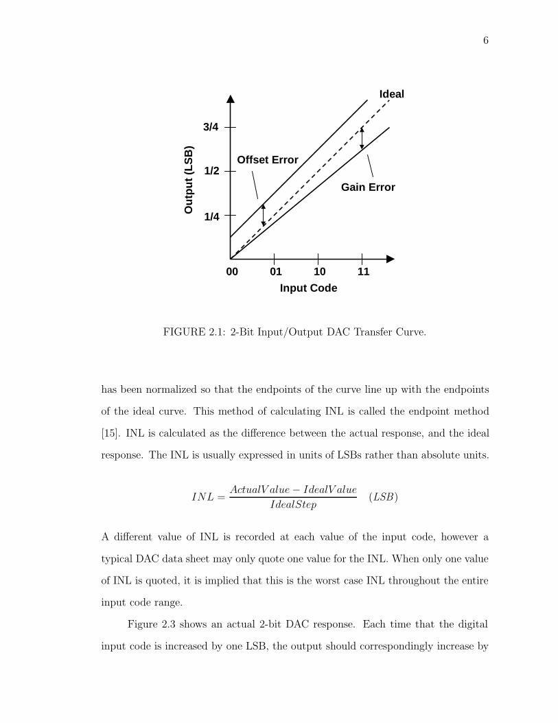
2.1 Static Performance Measures
Historically, the figures of merit that have received the most attention for
DACs are the static ones [2, 11]. The most common static figures of merit are integral
non-linearity (INL), differential non-linearity (DNL), and monotonicity. DACs also
commonly exhibit other characteristics that are not as frequently mentioned; namely
offset error and gain error. Figure 2.1 shows an input/output transfer curve for a
2-bit DAC. Both gain error an offset error are depicted in Fig. 2.1, with the ideal
transfer curve shown as a reference. It can be seen that the offset error is merely a
shift up or down of the entire curve. The gain error on the other hand can have points
in common with the ideal curve at the beginning or end, but the gain error curve
has a different slope than the ideal. The reason that these DAC characteristics
are not commonly mentioned is because they are easily corrected for, and often
cause no problems in certain applications even if they are not corrected [15]. Before
measuring INL, DNL, or monotonicity, it is assumed that both the gain error and
offset error have been corrected, so that ideal transfer curve becomes the reference
once again.
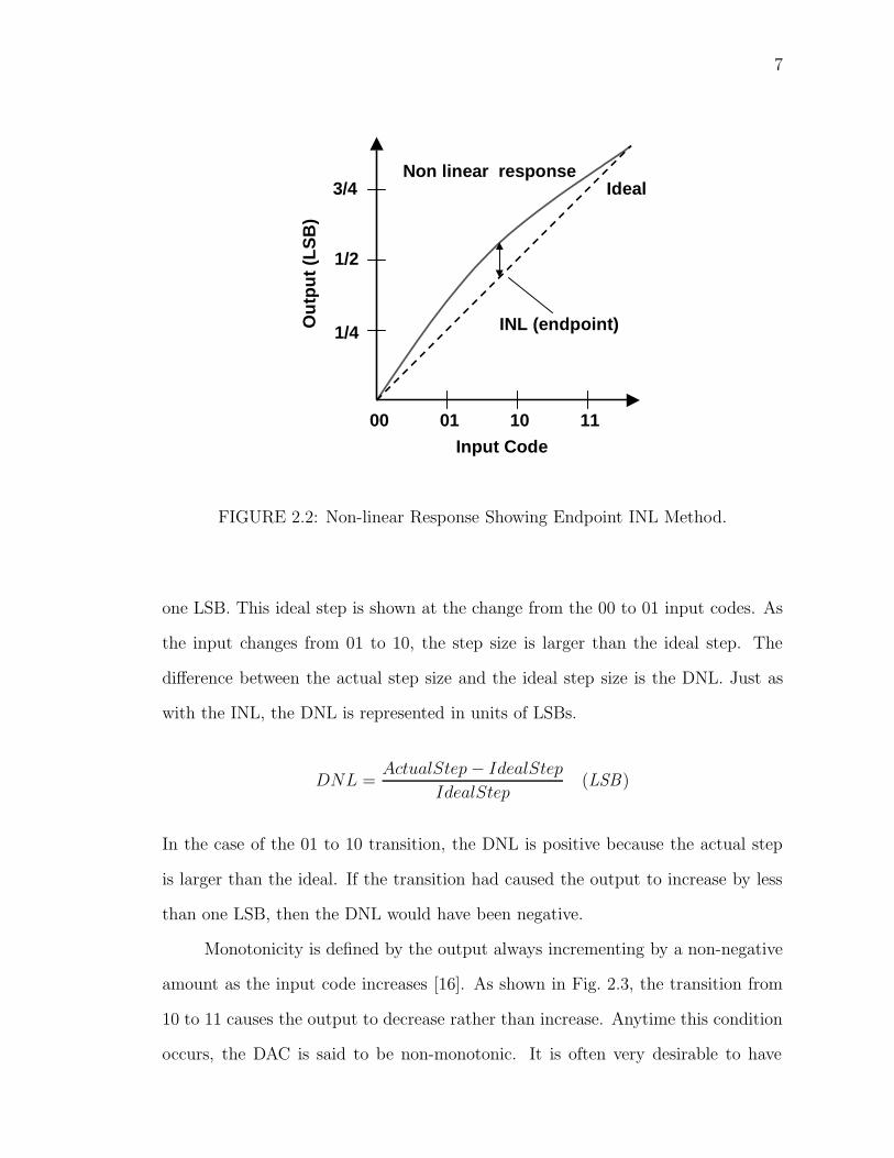
Figure 2.2 shows a typical non-linear DAC response. The non-linear curve
6
00 01 10 11
1/4
1/2
3/4
Offset Error
Gain Error
Ideal
Input Code
Out
put (
LSB
)
FIGURE 2.1: 2-Bit Input/Output DAC Transfer Curve.
has been normalized so that the endpoints of the curve line up with the endpoints
of the ideal curve. This method of calculating INL is called the endpoint method
[15]. INL is calculated as the difference between the actual response, and the ideal
response. The INL is usually expressed in units of LSBs rather than absolute units.
INL =ActualV alue− IdealV alue
IdealStep(LSB)
A different value of INL is recorded at each value of the input code, however a
typical DAC data sheet may only quote one value for the INL. When only one value
of INL is quoted, it is implied that this is the worst case INL throughout the entire
input code range.
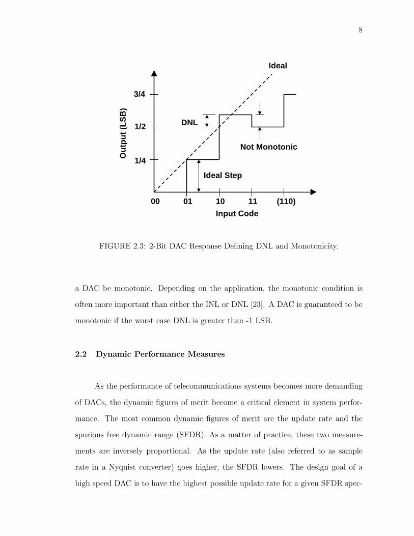
Figure 2.3 shows an actual 2-bit DAC response. Each time that the digital
input code is increased by one LSB, the output should correspondingly increase by
7
00 01 10 11
1/4
1/2
3/4
Input Code
Out
put (
LSB
)INL (endpoint)
IdealNon linear response
FIGURE 2.2: Non-linear Response Showing Endpoint INL Method.
one LSB. This ideal step is shown at the change from the 00 to 01 input codes. As
the input changes from 01 to 10, the step size is larger than the ideal step. The
difference between the actual step size and the ideal step size is the DNL. Just as
with the INL, the DNL is represented in units of LSBs.
DNL =ActualStep− IdealStep
IdealStep(LSB)
In the case of the 01 to 10 transition, the DNL is positive because the actual step
is larger than the ideal. If the transition had caused the output to increase by less
than one LSB, then the DNL would have been negative.
Monotonicity is defined by the output always incrementing by a non-negative
amount as the input code increases [16]. As shown in Fig. 2.3, the transition from
10 to 11 causes the output to decrease rather than increase. Anytime this condition
occurs, the DAC is said to be non-monotonic. It is often very desirable to have
8
00 01 10 11
1/4
1/2
3/4
Input Code
Out
put (
LSB
)DNL
Ideal
(110)
Ideal Step
Not Monotonic
FIGURE 2.3: 2-Bit DAC Response Defining DNL and Monotonicity.
a DAC be monotonic. Depending on the application, the monotonic condition is
often more important than either the INL or DNL [23]. A DAC is guaranteed to be
monotonic if the worst case DNL is greater than -1 LSB.
2.2 Dynamic Performance Measures
As the performance of telecommunications systems becomes more demanding
of DACs, the dynamic figures of merit become a critical element in system perfor-
mance. The most common dynamic figures of merit are the update rate and the
spurious free dynamic range (SFDR). As a matter of practice, these two measure-
ments are inversely proportional. As the update rate (also referred to as sample
rate in a Nyquist converter) goes higher, the SFDR lowers. The design goal of a
high speed DAC is to have the highest possible update rate for a given SFDR spec-
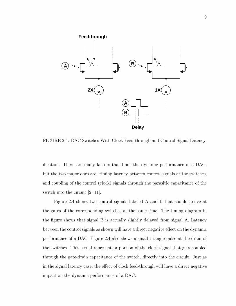
9
A
B
A B
Delay
Feedthrough
1X2X
FIGURE 2.4: DAC Switches With Clock Feed-through and Control Signal Latency.
ification. There are many factors that limit the dynamic performance of a DAC,
but the two major ones are: timing latency between control signals at the switches,
and coupling of the control (clock) signals through the parasitic capacitance of the
switch into the circuit [2, 11].
Figure 2.4 shows two control signals labeled A and B that should arrive at
the gates of the corresponding switches at the same time. The timing diagram in
the figure shows that signal B is actually slightly delayed from signal A. Latency
between the control signals as shown will have a direct negative effect on the dynamic
performance of a DAC. Figure 2.4 also shows a small triangle pulse at the drain of
the switches. This signal represents a portion of the clock signal that gets coupled
through the gate-drain capacitance of the switch, directly into the circuit. Just as
in the signal latency case, the effect of clock feed-through will have a direct negative
impact on the dynamic performance of a DAC.
10
3. DAC DESIGN
Now that the concepts behind digital to analog conversion have been intro-
duced the proposed 10-bit DAC is presented in detail. The DAC architecture is
segmented to utilize the performance advantages of thermometer coding on the
MSBs, while capitalizing on the area savings of the R-2R ladder for the LSBs. The
optimization of die area that resulted in the chosen architecture is discussed in
detail. A device mismatch analysis was performed in MATLAB to arrive at the
implemented design. A method for providing linear output currents from the DAC,
while at the same time overcoming the limitations proposed by the 1.8 V power
supply, will be presented. The design of the digital circuitry to control the switches
will be briefly explained before simulation results from MATLAB and SPICE are
presented. The detailed process guidelines of a standard digital 0.18 µm CMOS pro-
cess have been carefully considered to ensure DAC performance with temperature
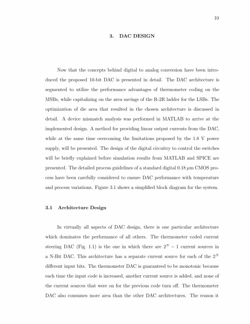
and process variations. Figure 3.1 shows a simplified block diagram for the system.
3.1 Architecture Design
In virtually all aspects of DAC design, there is one particular architecture
which dominates the performance of all others. The thermometer coded current
steering DAC (Fig. 1.1) is the one in which there are 2N − 1 current sources in
a N-Bit DAC. This architecture has a separate current source for each of the 2N
different input bits. The thermometer DAC is guaranteed to be monotonic because
each time the input code is increased, another current source is added, and none of
the current sources that were on for the previous code turn off. The thermometer
DAC also consumes more area than the other DAC architectures. The reason it
11
CurrentSource
VrefIout
CurrentSource
VrefIout
CurrentSource
VrefIout
-
+
Amp-
+
Amp
Resistors
CurrentSource
VrefIout
-
+
Amp
Bin
ary
Inpu
t Cod
e
OUT
IN
IN
DecodingLogic
LatchesVref
Vref
Vref
Output Current
Switches
FIGURE 3.1: System Block Diagram.
consumes a large area is because the digital decoding logic needed to convert from a
binary input code into a thermometer code becomes very large when the DAC has
a resolution above 5 or 6 bits.
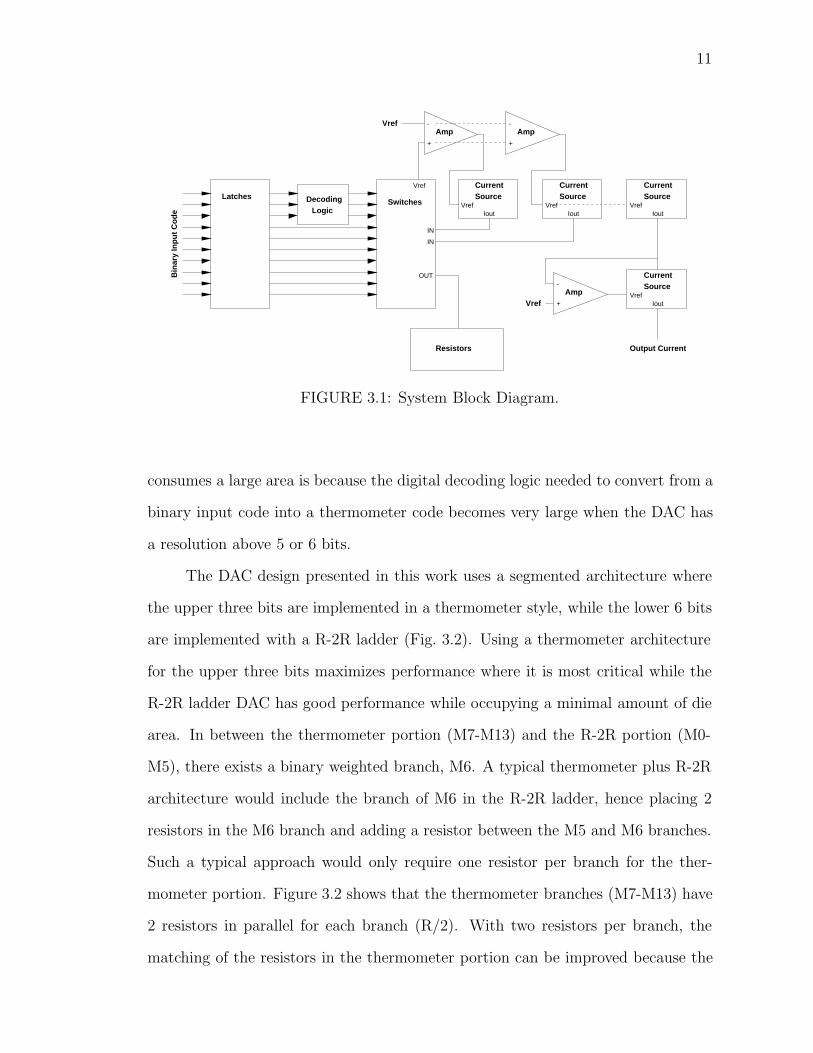
The DAC design presented in this work uses a segmented architecture where
the upper three bits are implemented in a thermometer style, while the lower 6 bits
are implemented with a R-2R ladder (Fig. 3.2). Using a thermometer architecture
for the upper three bits maximizes performance where it is most critical while the
R-2R ladder DAC has good performance while occupying a minimal amount of die
area. In between the thermometer portion (M7-M13) and the R-2R portion (M0-
M5), there exists a binary weighted branch, M6. A typical thermometer plus R-2R
architecture would include the branch of M6 in the R-2R ladder, hence placing 2
resistors in the M6 branch and adding a resistor between the M5 and M6 branches.
Such a typical approach would only require one resistor per branch for the ther-
mometer portion. Figure 3.2 shows that the thermometer branches (M7-M13) have
2 resistors in parallel for each branch (R/2). With two resistors per branch, the
matching of the resistors in the thermometer portion can be improved because the
12
effect of a linear process gradient can be eliminated by proper layout. Hence the
reason that the middle branch (M6) is binary weighted rather than included in the
R-2R portion.
Since this DAC operates from a single 1.8V power supply, the amount of
headroom left above the current steering circuitry is not sufficient for providing
output currents in a general application DAC. This low voltage limitation created
the design of the current mirror output circuit. The output currents are shown as
I1 and I2 in Fig. 3.2. The goal of the design is to achieve a linear and monotonic
output current while supplying maximum voltage headroom. By mirroring currents
off Mx1 and Mx2, the output nodes may be placed as high as 1.4V and still achieve
linear operation. The gate voltage is produced from the servoing op-amps shown
in Fig. 3.2. The servoing operation is an essential step in the functionality of the
DAC. The servo maintains a constant voltage (Vref) at the drains of Mx1 and Mx2,
regardless of the currents passing through them. If the output nodes are set to the
same Vref voltage, then the output currents I1 and I2 will be a perfectly linear replica
of the currents in Mx1 and Mx2. Servoing is the ideal solution to the headroom
problem associated with the low voltage supply because the drain voltages of Mx1
and Mx2 remain more stable than for a bipolar device, and the servo provides the
current mirror voltage at the same time.
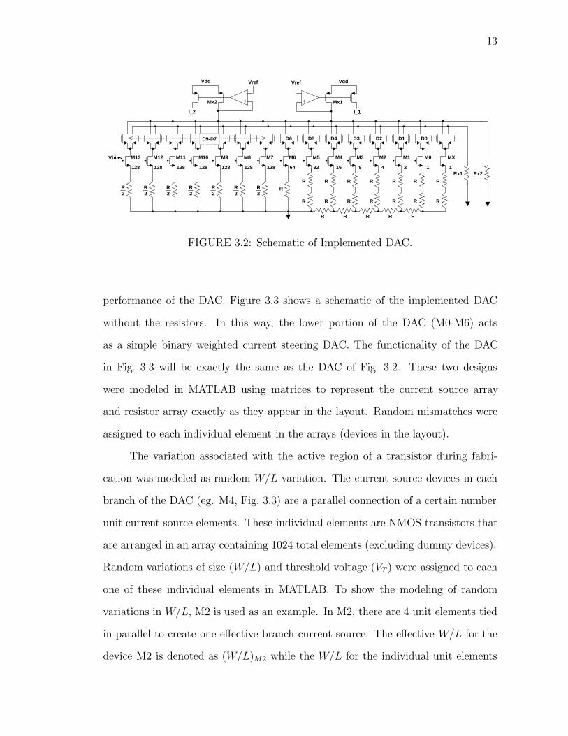
3.2 Mismatch Modeling for Architectural Optimization
At this point only DAC architectures with resistors present in the current
branches have been discussed, however the majority of the current steering DACs
recently published have been implemented without the use of resistors [2, 5, 11, 19,
20, 21]. An analysis was performed in MATLAB to examine the effects of adding
resistors below the current sources, and what effect device mismatch has on the
13
D0D1D2D3D4D5D6
Vbias
D9-D7
R
R
R
R
R
R
R
R
R
R
R
R
R
R
RRRRR
RR2
R2
R2
R2
R2
R2
R2
Rx1 Rx2
+
_
I_1
VddVref
+
_
I_2
Vdd Vref
M0M1M2M3M4M5M6M7M8M9M10M11M12M13
Mx2 Mx1
1 1248163264128128128128128128128
MX
FIGURE 3.2: Schematic of Implemented DAC.
performance of the DAC. Figure 3.3 shows a schematic of the implemented DAC
without the resistors. In this way, the lower portion of the DAC (M0-M6) acts
as a simple binary weighted current steering DAC. The functionality of the DAC
in Fig. 3.3 will be exactly the same as the DAC of Fig. 3.2. These two designs
were modeled in MATLAB using matrices to represent the current source array
and resistor array exactly as they appear in the layout. Random mismatches were
assigned to each individual element in the arrays (devices in the layout).
The variation associated with the active region of a transistor during fabri-
cation was modeled as random W/L variation. The current source devices in each
branch of the DAC (eg. M4, Fig. 3.3) are a parallel connection of a certain number
unit current source elements. These individual elements are NMOS transistors that
are arranged in an array containing 1024 total elements (excluding dummy devices).
Random variations of size (W/L) and threshold voltage (VT ) were assigned to each
one of these individual elements in MATLAB. To show the modeling of random
variations in W/L, M2 is used as an example. In M2, there are 4 unit elements tied
in parallel to create one effective branch current source. The effective W/L for the
device M2 is denoted as (W/L)M2 while the W/L for the individual unit elements
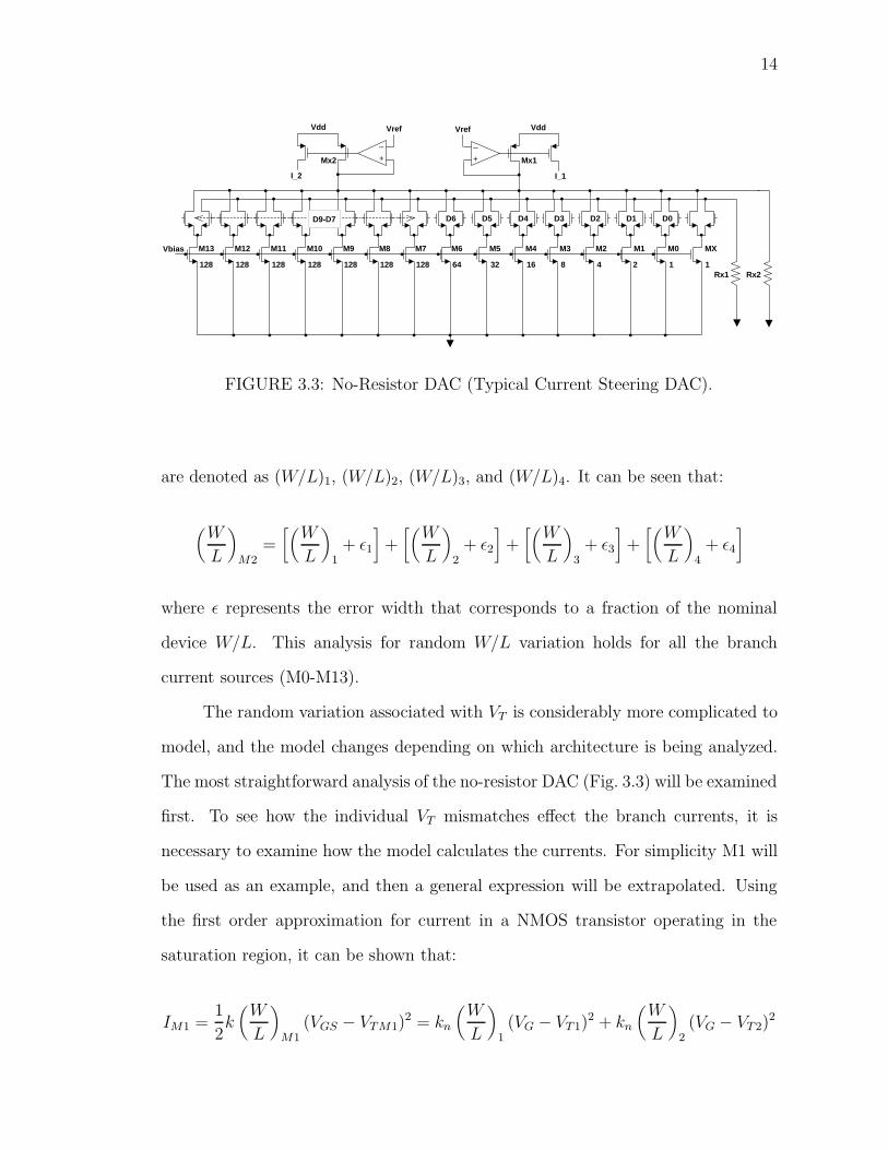
14
D0D1D2D3D4D5D6
Vbias
D9-D7
Rx1 Rx2
+
_
I_1
VddVref
+
_
I_2
Vdd Vref
M0M1M2M3M4M5M6M7M8M9M10M11M12M13
Mx2 Mx1
1 1248163264128128128128128128128
MX
FIGURE 3.3: No-Resistor DAC (Typical Current Steering DAC).
are denoted as (W/L)1, (W/L)2, (W/L)3, and (W/L)4. It can be seen that:
(W
L
)M2
=[(W
L
)1
+ ε1
]+[(W
L
)2
+ ε2
]+[(W
L
)3
+ ε3
]+[(W
L
)4
+ ε4
]
where ε represents the error width that corresponds to a fraction of the nominal
device W/L. This analysis for random W/L variation holds for all the branch
current sources (M0-M13).
The random variation associated with VT is considerably more complicated to
model, and the model changes depending on which architecture is being analyzed.
The most straightforward analysis of the no-resistor DAC (Fig. 3.3) will be examined
first. To see how the individual VT mismatches effect the branch currents, it is
necessary to examine how the model calculates the currents. For simplicity M1 will
be used as an example, and then a general expression will be extrapolated. Using
the first order approximation for current in a NMOS transistor operating in the
saturation region, it can be shown that:
IM1 =1
2k(W
L
)M1
(VGS − VTM1)2 = kn
(W
L
)1
(VG − VT1)2 + kn
(W
L
)2
(VG − VT2)2
15
Where kn is equal to: kn = 12k = 1
2µnCox. Multiplying through and expanding;
IM1 = kn
(W
L
)1
(V 2G − 2VGVT1 + V 2
T1) + kn
(W
L
)2
(V 2G − 2VGVT2 + V 2
T2)
Where: VT1 = VTi + ε1 and VT2 = VTi + ε2. This result for a branch current
source with only two unit elements can be extrapolated to a general case that
accommodates all the branch current sources (M0-M13).
I = knV2G
2N∑j=1
(W
L
)j
+ kn2N∑j=1
(W
L
)jV 2Tj − 2VGkn
2N∑j=1
(W
L
)jVTj
Next, the branch currents for the resistor style DAC (Fig. 3.2) are solved.
Since the source terminals of the current sources in the resistor DAC are not tied
together at a common potential, the complexity of the model increases. Additional
complexity is also added because the body effect of the unit elements was modeled for
the current sources in this DAC. The threshold voltage for a unit element including
the body effect is written as: VT = VTO + γ(√
VSB+ | 2φF | −√| 2φF |
)where
γ =√
2qNAKSεO/COX. Both γ and φF can be assumed as constants and taken
directly from the process specifications. If γ and φF are both taken as constants, then
the only variable upon which the body effect depends is the source-bulk potential,
VSB. Since the bulk of the NMOS device is the silicon substrate, and it is connected
to ground, VSB is simply the source voltage (VS), and will be referred to as such
from here on.
The model for the branch currents in the resistor DAC (Fig. 3.2) is different
for current sources M5-M13 than it is for current sources MX-M4. This difference
arises because the voltages between the resistors in the R-2R ladder are not known,
and therefore need to be solved iteratively. For the resistors in the upper portion
however, one side is tied to ground, and the analysis is simplified. The model for
16
the upper portion will be examined first. For simplicity of this derivation, current
source M6 is assumed to have only 2 unit elements rather than 64, then a general
equation is extrapolated which accurately models M5-M13.
IM6 = kn
(W
L
)1
(VG − VS − VT1)2 + kn
(W
L
)2
(VG − VS − VT2)2
Where: VS = IR. Multiplying through and expanding;
IM6 = kn
(W
L
)1
[I2R2 + 2VT1IR− 2VGIR+ V 2T1 + V 2
G − 2VGVT1] + ...
kn
(W
L
)2
[I2R2 + 2VT2IR− 2VGIR+ V 2T2 + V 2
G − 2VGVT2]
Since the result is a quadratic function, the I terms are collected and the equation
is set equal to zero. For simplicity, kn(WL
)1
is written as K1 and kn(WL
)2
is K2.
I2(K1R2 +K2R
2) + I(2K1VT1R+ 2K2VT2R− 2K1VGR− 2K2VGR− 1) + ...
K1(V 2T1 + V 2
G − 2VGVT1) +K2(V 2T2 + V 2
G − 2VGVT2) = 0
Each term can be collected and represented generally as:
I2 Term = R2kn2N∑j=1
(W
L
)j
I Term = 2Rkn2N∑j=1
(W
L
)jVTj − 2RVGkn
2N∑j=1
(W
L
)j− 1
Constant Term = V 2Gkn
2N∑j=1
(W
L
)j
+ kn2N∑j=1
(W
L
)jV 2Tj − 2knVG
2N∑j=1
(W
L
)jVTj
These quadratic terms were used in MATLAB to solve the branch currents
for M5-M13. The MATLAB model works iteratively to solve these branch currents
because the branch current is dependent on VT , and VT is dependent on the source
17
voltage (VS), which in turn, is dependent on the branch current and the resistance.
The final DAC currents that need to be solved are the R-2R currents of MX-M4.
In this derivation, M1 is used as an example. It can be seen that:
IM1 = kn
(W
L
)1
(VG − VS1 − VT1)2 + kn
(W
L
)2
(VG − VS1 − VT2)2
Multiplying through and expanding all squared terms;
IM1 = kn
(W
L
)1
[V 2G − 2VGVS1 − 2VGVT1 + 2VS1VT1 + V 2
T1 + V 2S1] + ...
kn
(W
L
)2
[V 2G − 2VGVS1 − 2VGVT2 + 2VS1VT2 + V 2
T2 + V 2S1]
Collecting all terms and extrapolating a general equation:
Ix = kn[V 2G−2VGVSx+V
2Sx]
2N∑j=1
(W
L
)j+2kn[VSx−VG]
2N∑j=1
(W
L
)jVTj+kn
2N∑j=1
(W
L
)jV 2Tj
With both the resistor DAC of Fig. 3.2 and the no-resistor DAC of Fig. 3.3
accurately modeled in MATLAB, an analysis was performed to quantify the effects
of device mismatch on DAC performance.
3.2.1 Resistor vs. No-Resistor Designs
Accurate modeling of the resistor and no-resistor DACs allowed for side by
side comparison of the two architectures given a certain set of mismatch parameters.
The three mismatch parameters: σW , σVT , and σR are related to the parameters in
the MATLAB model as follows: WL
= WL
(1 + σW ), VT = VT (1 + σVT ), and R =
R(1 + σR), where σ represents a normally distributed random number with zero
mean and a variance of 1.0. Figure 3.4 shows the INL and DNL performance of
18
0 200 400 600 800 10000
0.5
1
1.5
2
Input Code
DN
L (L
SB
)
RMS DNL for Implemented DAC
0 200 400 600 800 10000
0.5
1
1.5
2
2.5
Input Code
INL
(LS
B)
RMS INL for Implemented DAC
0 200 400 600 800 10000
0.5
1
1.5
2
Input Code
DN
L (L
SB
)
RMS DNL for No Resistor DAC
0 200 400 600 800 10000
0.5
1
1.5
2
2.5
Input Code
INL
(LS
B)
RMS INL for No Resistor DAC
FIGURE 3.4: INL and DNL Performance of Resistor DAC and No-Resistor DAC.
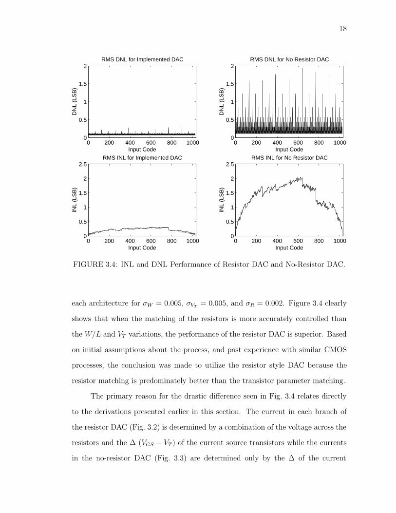
each architecture for σW = 0.005, σVT = 0.005, and σR = 0.002. Figure 3.4 clearly
shows that when the matching of the resistors is more accurately controlled than
the W/L and VT variations, the performance of the resistor DAC is superior. Based
on initial assumptions about the process, and past experience with similar CMOS
processes, the conclusion was made to utilize the resistor style DAC because the
resistor matching is predominately better than the transistor parameter matching.
The primary reason for the drastic difference seen in Fig. 3.4 relates directly
to the derivations presented earlier in this section. The current in each branch of
the resistor DAC (Fig. 3.2) is determined by a combination of the voltage across the
resistors and the ∆ (VGS − VT ) of the current source transistors while the currents
in the no-resistor DAC (Fig. 3.3) are determined only by the ∆ of the current
19
source transistors. Therefore, as the matching of the resistors becomes better than
the matching of the current source devices, the performance of the resistor DAC
dominates. Likewise, as the voltage across the resistors becomes larger in the resistor
DAC, the performance improves further. The area consumed by the resistors has
to be carefully considered when deciding how large the voltage drop should be. In
the design presented, the resistors were optimized to provide the best performance
while consuming a minimal area.
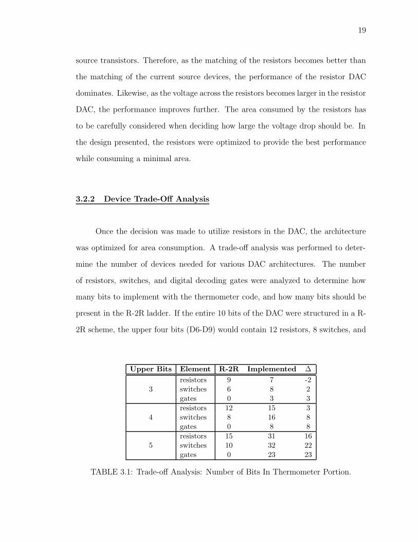
3.2.2 Device Trade-Off Analysis
Once the decision was made to utilize resistors in the DAC, the architecture
was optimized for area consumption. A trade-off analysis was performed to deter-
mine the number of devices needed for various DAC architectures. The number
of resistors, switches, and digital decoding gates were analyzed to determine how
many bits to implement with the thermometer code, and how many bits should be
present in the R-2R ladder. If the entire 10 bits of the DAC were structured in a R-
2R scheme, the upper four bits (D6-D9) would contain 12 resistors, 8 switches, and
Upper Bits Element R-2R Implemented ∆resistors 9 7 -2
3 switches 6 8 2gates 0 3 3resistors 12 15 3
4 switches 8 16 8gates 0 8 8resistors 15 31 16
5 switches 10 32 22gates 0 23 23
TABLE 3.1: Trade-off Analysis: Number of Bits In Thermometer Portion.
20
zero logic gates. In the segmented architecture that was implemented, the upper
four bits contain 15 resistors, 16 switches and 8 logic gates.
Table 3.1 shows a summary of the number of resistors, switches, and 2-input
logic gates needed to implement the upper 3, 4, or 5 bits. The binary bit that
exists between the thermometer and R-2R portions of the implemented architecture
is included in the 3, 4, or 5 bits examined in the table. Table 3.1 shows that
the device increase from the full R-2R ladder to the implemented architecture is
acceptable for 3 and 4 upper bits, but the increase in number of resistors, switches,
and gates is not acceptable for 5 upper bits.
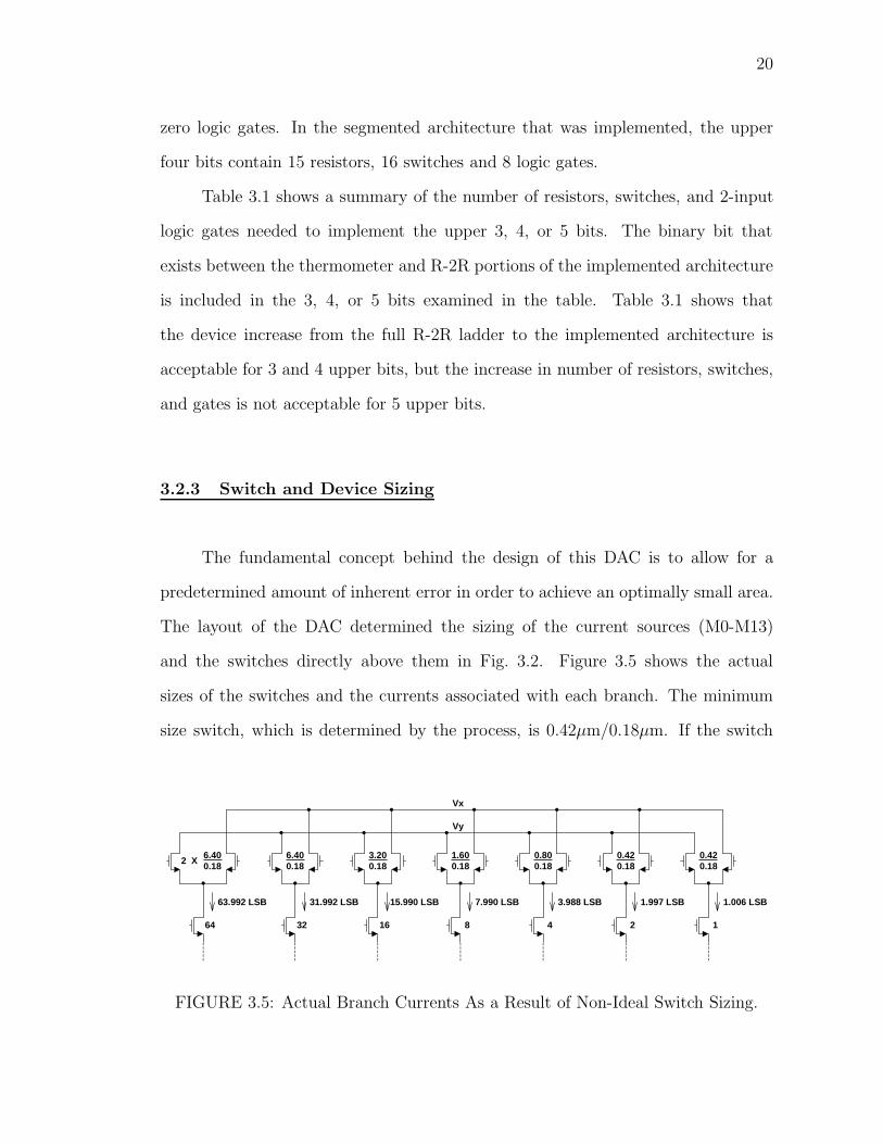
3.2.3 Switch and Device Sizing
The fundamental concept behind the design of this DAC is to allow for a
predetermined amount of inherent error in order to achieve an optimally small area.
The layout of the DAC determined the sizing of the current sources (M0-M13)
and the switches directly above them in Fig. 3.2. Figure 3.5 shows the actual
sizes of the switches and the currents associated with each branch. The minimum
size switch, which is determined by the process, is 0.42µm/0.18µm. If the switch
0.420.18
1
0.420.18
2
0.800.18
4
1.600.18
8
6.400.18
64
3.200.18
16
6.400.18
32
2 X
1.997 LSB
Vx
Vy
1.006 LSB3.988 LSB7.990 LSB15.990 LSB31.992 LSB63.992 LSB
FIGURE 3.5: Actual Branch Currents As a Result of Non-Ideal Switch Sizing.
21
0 200 400 600 800 10000
0.1
0.2
0.3
0.4
0.5
Input Code
DN
L (L
SB
)
RMS DNL for Mismatch Case 1
0 200 400 600 800 10000
0.1
0.2
0.3
0.4
0.5
0.6
0.7
Input Code
INL
(LS
B)
RMS INL for Mismatch Case 1
0 200 400 600 800 10000
0.1
0.2
0.3
0.4
0.5
Input Code
DN
L (L
SB
)
RMS DNL for Mismatch Case 2
0 200 400 600 800 10000
0.1
0.2
0.3
0.4
0.5
0.6
Input Code
INL
(LS
B)
RMS INL for Mismatch Case 2
FIGURE 3.6: Simulations of Mismatch in the Implemented Architecture.
sizing had been perfectly ideal, the switch above the 2X current source would be
2 × 0.42µm/0.18µm rather than the implemented 0.42µm/0.18µm size. The errors
caused by non-ideal scaling of these switches are present because each switch does
not have the same voltage drop, and therefore the current sources do not have
the same drain-source voltages (VDS). The finite difference in VDS for the current
sources causes the currents in each branch to be slightly less than ideal, but still
well within the predetermined error budget.
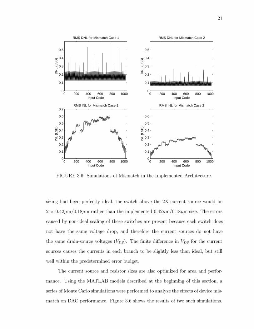
The current source and resistor sizes are also optimized for area and perfor-
mance. Using the MATLAB models described at the beginning of this section, a
series of Monte Carlo simulations were performed to analyze the effects of device mis-
match on DAC performance. Figure 3.6 shows the results of two such simulations.
22
VDD
+
_Vref
VDD
+
_
Vref
Iout
DAC
A B
M1
M2M3
Amp1
FIGURE 3.7: Simplified DAC Schematic With Linear Output Current Mirror.
Mismatch case 1 used the following parameter variations: σW = 0.01, σVT = 0.01,
and σR = 0.004; while mismatch case 2 used the following: σW = 0.005, σVT = 0.005,
and σR = 0.002. Although the expected matching from the process more closely
correlates to case 2, Fig. 3.6 shows that even when the device mismatches are double
the predicted values, the INL and DNL are well within the 10-Bit performance level.
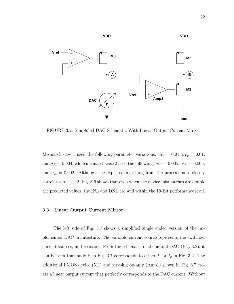
3.3 Linear Output Current Mirror
The left side of Fig. 3.7 shows a simplified single ended version of the im-
plemented DAC architecture. The variable current source represents the switches,
current sources, and resistors. From the schematic of the actual DAC (Fig. 3.2), it
can be seen that node B in Fig. 3.7 corresponds to either I1 or I2 in Fig. 3.2. The
additional PMOS device (M1) and servoing op-amp (Amp1) shown in Fig. 3.7 cre-
ate a linear output current that perfectly corresponds to the DAC current. Without
23
T0
T0n
T1
T1n
T2
T2n
T4
T6n
T6
T5n
T5
T4n
D9 D8 D7
FIGURE 3.8: Decoding Logic For Binary to Thermometer Code.
these additional devices, node B would be free to change voltage depending on the
output circuitry. Any variation in the voltage at node B will cause the currents
in M2 and M3 to be slightly different, and hence will introduce non-linearity. The
high gain servo created by Amp1 and M1, forces nodes A and B to the same voltage
(Vref). The design of this output stage maintains a linear output current while the
output node (Iout) is allowed to vary from 0V to 1.0 V, which is more than half of
the available 1.8V power supply.
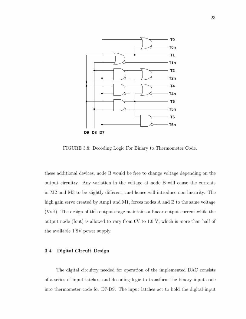
3.4 Digital Circuit Design
The digital circuitry needed for operation of the implemented DAC consists
of a series of input latches, and decoding logic to transform the binary input code
into thermometer code for D7-D9. The input latches act to hold the digital input
24
0 100 200 300 400 500 600 700 800 900 1000−0.02
−0.01
0
0.01
0.02INL
INL
(LS
B)
Input Code
0 100 200 300 400 500 600 700 800 900 1000−0.02
−0.01
0
0.01
0.02DNL
INL
(LS
B)
Input Code
FIGURE 3.9: Simulated INL and DNL For Implemented 10-Bit DAC.
value at the inputs of the switches regardless of what is happening on the system
digital bus. These latches are simple inverters connected back to back with a pass
transistor. The decoding logic needed to transform the binary input code into a
thermometer code is shown in Fig. 3.8. D7, D8, and D9 are the binary input bits,
and T0-T6n are the differential thermometer code outputs. T0 and T0n correspond
to branch M7, while T6 and T6n correspond to M13. T3 and T3n are not shown in
Fig. 3.8 because they are equivalent to D9 and D9n. A minimum number of logic
gates were used, and all the transistors that compose the actual gates are minimum
sized devices in order to keep the area required to a minimum.
25
0 100 200 300 400 500 600 700 800 900 1000−0.06
−0.04
−0.02
0
0.02
0.04
0.06INL
INL
(LS
B)
Input Code
0 100 200 300 400 500 600 700 800 900 1000−0.02
−0.01
0
0.01
0.02DNL
DN
L (L
SB
)
Input Code
FIGURE 3.10: INL and DNL of Current Mirror Output With Finite Op-Amp Gain.
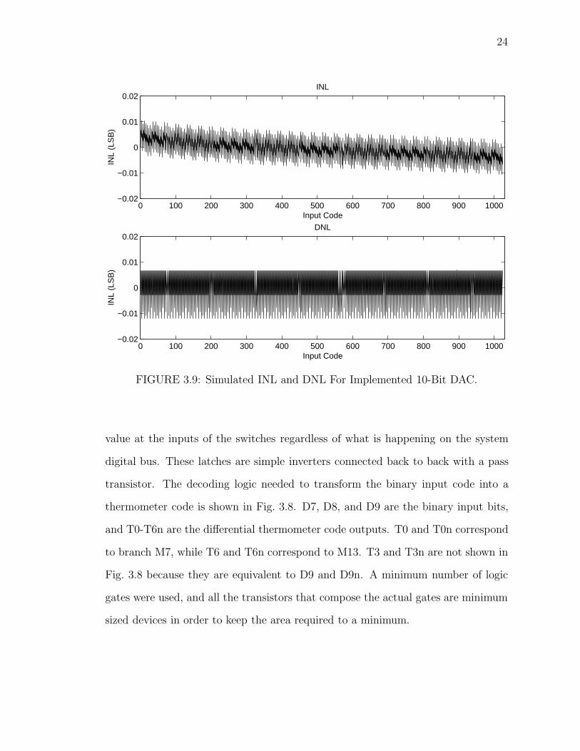
3.5 Simulation Results
Once the various DACs had been simulated and optimized in MATLAB to
reach the optimal architecture, the DAC of Fig. 3.2 was designed using the results
from SPICE simulations. Figure 3.9 shows the final DAC INL and DNL for the
implemented design. Simulation results show that even with the slight error in
branch currents due to non-ideal switch sizing, the INL and DNL are less than 0.02
LSB.
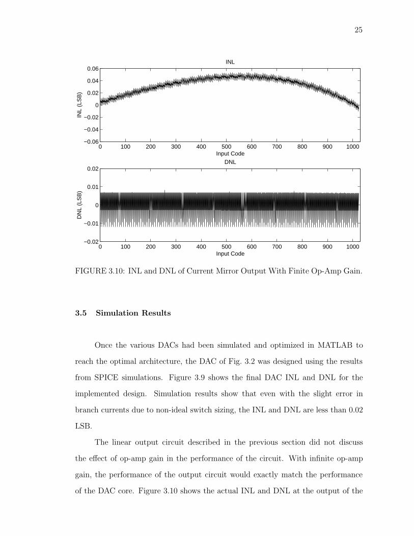
The linear output circuit described in the previous section did not discuss
the effect of op-amp gain in the performance of the circuit. With infinite op-amp
gain, the performance of the output circuit would exactly match the performance
of the DAC core. Figure 3.10 shows the actual INL and DNL at the output of the
26
0 100 200 300 400 500 600 700 800 900 1000
−0.8
−0.6
−0.4
−0.2
0
INL
INL
(LS
B)
Input Code
0 100 200 300 400 500 600 700 800 900 1000−0.02
−0.01
0
0.01
0.02DNL
DN
L (L
SB
)
Input Code
FIGURE 3.11: INL and DNL for Ideal Current Mirror With 10mV Offset.
mirroring circuit. The slight degradation in the simulated INL is present because of
the finite op-amp gain in the output circuit. Since the gain of the op-amp is finite,
node B in Fig. 3.7 is allowed to slightly change as the current in the DAC changes.
The error caused by the finite op-amp gain effect is negligible as the INL is less than
0.06 LSB.
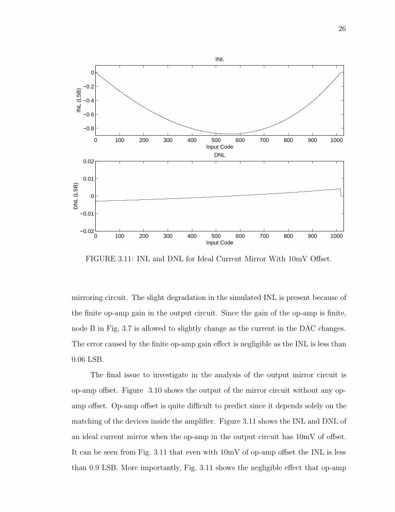
The final issue to investigate in the analysis of the output mirror circuit is
op-amp offset. Figure 3.10 shows the output of the mirror circuit without any op-
amp offset. Op-amp offset is quite difficult to predict since it depends solely on the
matching of the devices inside the amplifier. Figure 3.11 shows the INL and DNL of
an ideal current mirror when the op-amp in the output circuit has 10mV of offset.
It can be seen from Fig. 3.11 that even with 10mV of op-amp offset the INL is less
than 0.9 LSB. More importantly, Fig. 3.11 shows the negligible effect that op-amp
27
0 100 200 300 400 500 600 700 800 900 1000
−0.8
−0.6
−0.4
−0.2
0
INL
INL
(LS
B)
Input Code
0 100 200 300 400 500 600 700 800 900 1000−0.02
−0.01
0
0.01
0.02DNL
DN
L (L
SB
)
Input Code
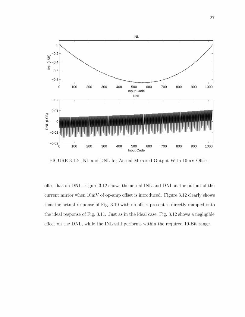
FIGURE 3.12: INL and DNL for Actual Mirrored Output With 10mV Offset.
offset has on DNL. Figure 3.12 shows the actual INL and DNL at the output of the
current mirror when 10mV of op-amp offset is introduced. Figure 3.12 clearly shows
that the actual response of Fig. 3.10 with no offset present is directly mapped onto
the ideal response of Fig. 3.11. Just as in the ideal case, Fig. 3.12 shows a negligible
effect on the DNL, while the INL still performs within the required 10-Bit range.
28
4. ULTRA HIGH GAIN OP-AMP DESIGN
Operational amplifiers (op-amps) are one of the key building blocks in today’s
mixed-signal area. Extensive research has been done in the op-amp area to achieve
all sorts of different results. Research of general purpose op-amps is slowly becoming
a thing of the past, where now op-amps are often designed with a specific applica-
tion in mind. Some applications require op-amps with extremely high bandwidth,
while others may require ultra high gain, low noise, low DC offset, fast settling time,
or just about any combination of these parameters. This chapter introduces a few
basic op-amp architectures as well as the basic figures of merit used in the design
process. The novel feed-forward architecture and extensive MATLAB modeling of
the implemented op-amp are presented. Design considerations for the low voltage
operation of the op-amp will be briefly discussed before the results of SPICE sim-
ulations are presented. Just as in the case of the DAC design, extensive use of the
0.18 µm CMOS process specifications are used to ensure op-amp performance over
the wide range of temperature and process variations.
4.1 Op-Amp Basics
Figure 4.1 shows simplified schematics of the two most common op-amp ar-
chitectures. The gain of a single stage is simply the transconductance (gm) of the
input transistor multiplied by the impedance seen at the output node (Rout), there-
fore gain is V outV in
= gmin × Rout. The cascaded op-amp uses a chain of simple gain
stages to achieve higher gain at the output. Since the gain of the first stage is multi-
plied by the gain of the second stage, the total output gain is V outV in
= gm1ro1∗gm2ro2.
The cascode op-amp of Fig. 4.1 uses a stacking method to create a higher output
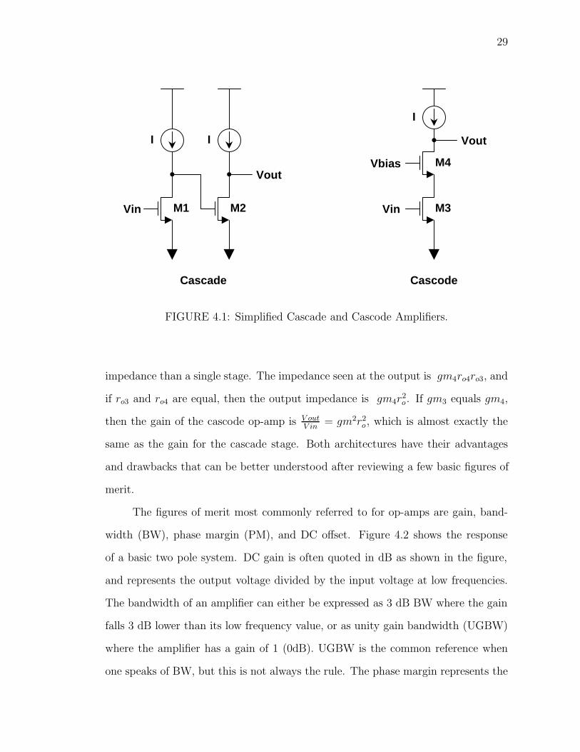
29
CascodeCascade
Vin
Vbias
I I
I
Vout
Vout
Vin M1 M2 M3
M4
FIGURE 4.1: Simplified Cascade and Cascode Amplifiers.
impedance than a single stage. The impedance seen at the output is gm4ro4ro3, and
if ro3 and ro4 are equal, then the output impedance is gm4r2o. If gm3 equals gm4,
then the gain of the cascode op-amp is V outV in
= gm2r2o, which is almost exactly the
same as the gain for the cascade stage. Both architectures have their advantages
and drawbacks that can be better understood after reviewing a few basic figures of
merit.
The figures of merit most commonly referred to for op-amps are gain, band-
width (BW), phase margin (PM), and DC offset. Figure 4.2 shows the response
of a basic two pole system. DC gain is often quoted in dB as shown in the figure,
and represents the output voltage divided by the input voltage at low frequencies.
The bandwidth of an amplifier can either be expressed as 3 dB BW where the gain
falls 3 dB lower than its low frequency value, or as unity gain bandwidth (UGBW)
where the amplifier has a gain of 1 (0dB). UGBW is the common reference when
one speaks of BW, but this is not always the rule. The phase margin represents the
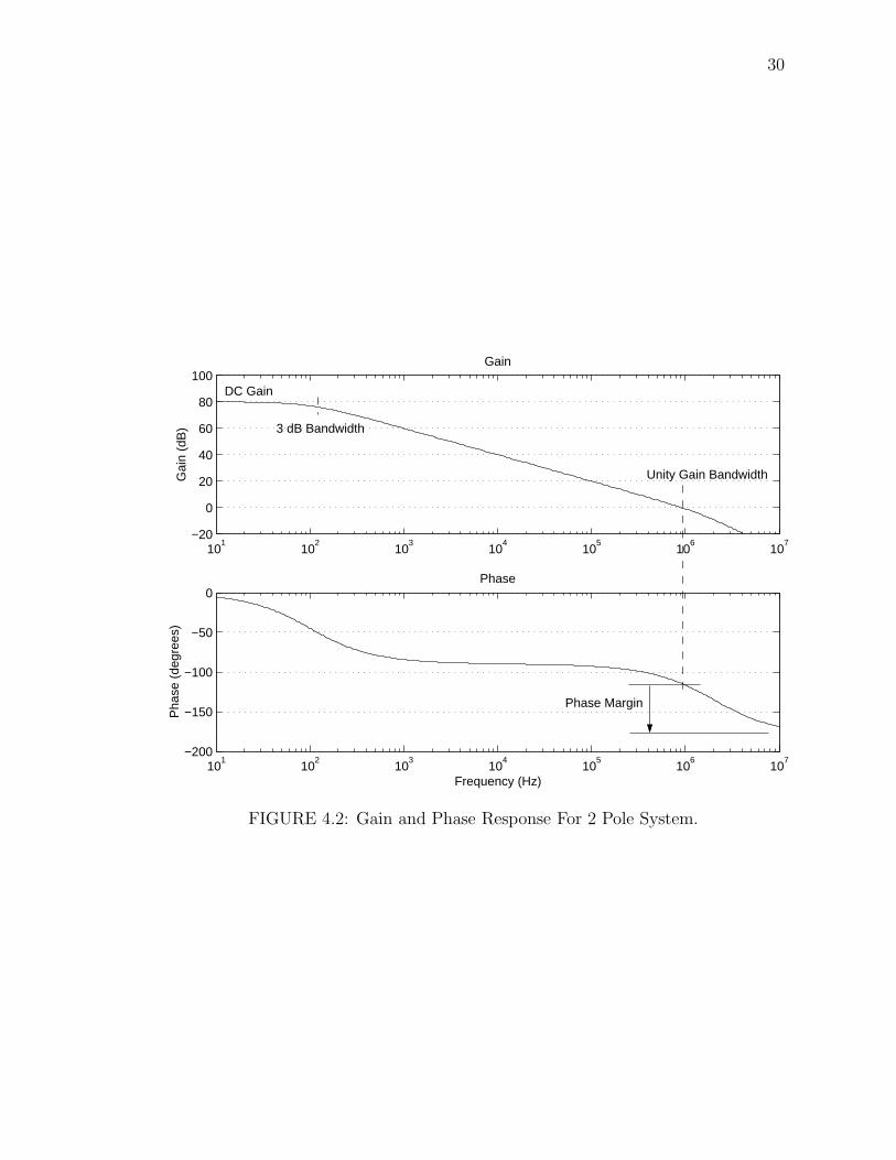
30
101
102
103
104
105
106
107
−20
0
20
40
60
80
100Gain
Gai
n (d
B)
101
102
103
104
105
106
107
−200
−150
−100
−50
0Phase
Frequency (Hz)
Pha
se (
degr
ees)
Phase Margin
Unity Gain Bandwidth
DC Gain
3 dB Bandwidth
FIGURE 4.2: Gain and Phase Response For 2 Pole System.
31
difference between the phase of the output signal and −180◦. The phase margin is
usually the greatest indicator of op-amp stability. When the phase margin is high
(eg. phase of output is −100◦), the settling time behavior of the op-amp will be
good because the op-amp is very stable. As the phase of the output signal gets
close to −180◦, the op-amp approaches an unstable condition where the output will
oscillate.
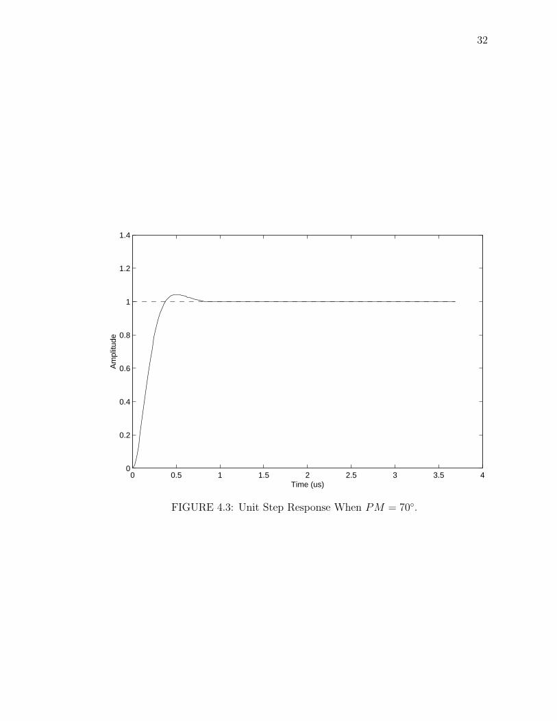
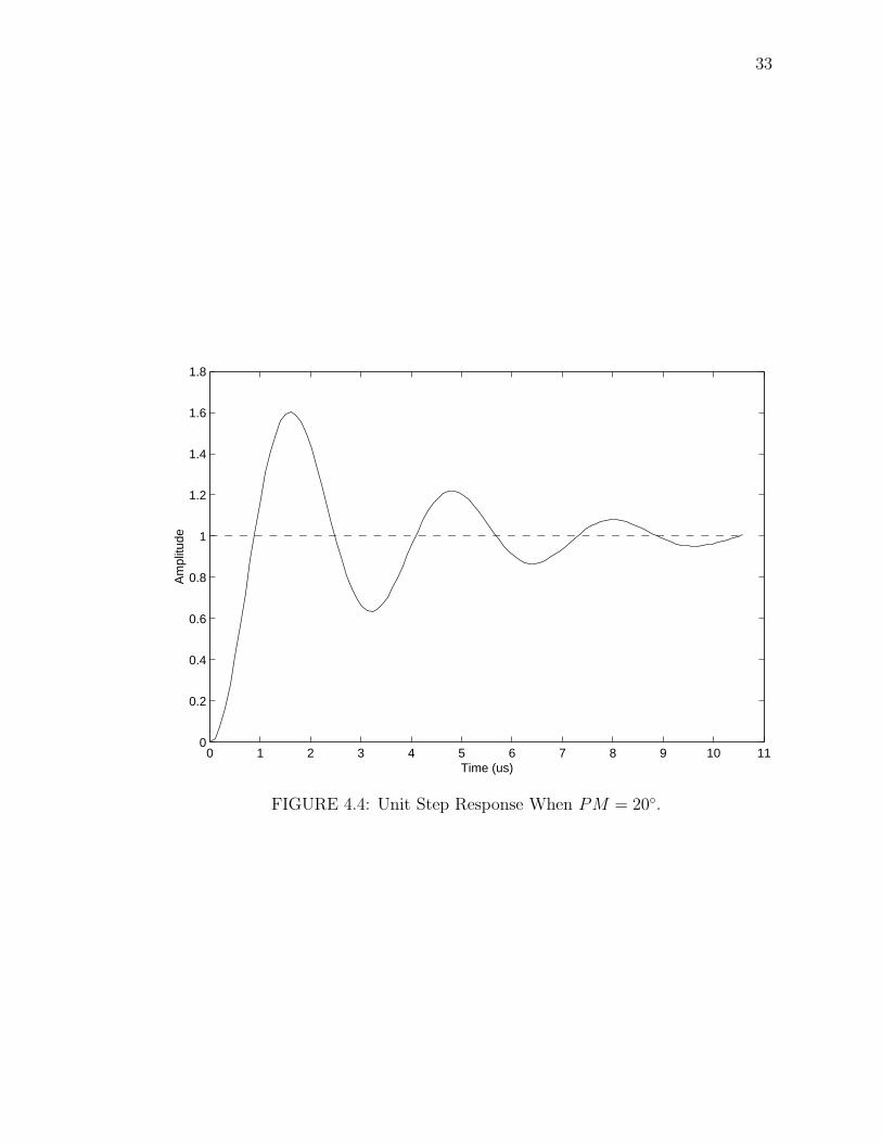
Figure 4.3 shows the settling behavior of a basic two pole op-amp in unity
gain configuration with a phase margin of 70◦ when a 1 V step is applied to the
input. Figure 4.4 shows the settling behavior of the same circuit, but with only 20◦
of phase margin. The ringing behavior seen in Fig. 4.4 is a good indicator that the
op-amp is near the unstable condition. If the phase margin had been closer to zero,
the output response would show a continuous oscillation, with little to no damping.
DC offset is the difference between the voltages at the inputs of an op-amp when
connected in the unity gain configuration. If the non-inverting input is set to 1V,
and the output (inverting input) has a voltage of 1.010V, then the op-amp offset
is 10mV. Op-amp offset has negative effects in almost all applications, and is often
eliminated by calibration in the continuous time or cancelled with capacitors in a
sampled-data system.
4.2 Architecture Design
The application for an op-amp that presents itself repeatedly in the DAC
design is servoing. In order to have an accurate servo, the op-amp which acts
as the servoing device needs to have a very high DC gain. As discussed briefly in
section 4.1, both the cascade and cascode op-amps of Fig. 4.1 allow for high DC gain.
The primary problem associated with the cascode op-amp is a lack of headroom.
Since the DAC and op-amp can only operate from a 1.8V power supply, limitations
32
0 0.5 1 1.5 2 2.5 3 3.5 40
0.2
0.4
0.6
0.8
1
1.2
1.4
Time (us)
Am
plitu
de
FIGURE 4.3: Unit Step Response When PM = 70◦.
33
0 1 2 3 4 5 6 7 8 9 10 110
0.2
0.4
0.6
0.8
1
1.2
1.4
1.6
1.8
Time (us)
Am
plitu
de
FIGURE 4.4: Unit Step Response When PM = 20◦.
34
are quickly introduced for the cascode design. The amount of drain-source voltage
available for each transistor in a cascode design with a 1.8V power supply is quite
limited. This limited drain-source voltage upon biasing implies that the output
voltage is not allowed to change very much without either the upper or lower (M3,
M4, Fig. 4.1) devices entering the triode region. In order to maintain high output
impedance, and hence high gain, the devices are not allowed to enter the triode
region at any point of operation.
Since the low voltage power supply limits the use of cascoding in this design,
a cascaded architecture is chosen. The primary problem associated with cascading
op-amps is the phase of the output signal. Figure 4.5 shows a cascade of 4 ideal
op-amps. Each op-amp represented by the ideal block is considered a single pole
system, which means that each stage introduces 90◦ of phase lag. If each stage adds
90◦ of phase lag, then the output signal will have a phase of −360◦. As mentioned
in section 4.1, an output signal with phase less than −180◦ will be unstable, and
therefore useless as an op-amp.
The architecture chosen to eliminate the problems associated with the stability
of a cascaded system is feed-forward compensation. This method of compensation,
shown in Fig. 4.6, allows the input signal to travel through the path composed
of A1-A4 at low frequencies, while high frequency inputs travel through the path
composed of A1 and Aff . Therefore, the op-amp performs as a 4 stage cascaded
op-amp at low frequencies to achieve ultra high DC gain, and as a 2 stage op-amp
at high frequencies to allow for a sufficient phase margin at the UGBW. Figure 4.6
+
_
VrefA A A
Vin
Vout
FIGURE 4.5: Cascade of Ideal Op-Amps.
35
+
_Vref
Aff
VDD
A2 A3 A4A1 M1
DAC
FIGURE 4.6: Feed-Forward Amplifier With Feedback.
shows the closed loop servoing operation of the op-amp. The device being servoed
(M1) acts as a gain stage in the feedback loop, and therefore must be included in
the simulation of the amplifier. The design must be performed such that there is
sufficient phase margin around the loop, therefore M1 is included in the op-amp
schematics and simulations, even though it is not technically a part of the op-amp.
4.3 MATLAB Modeling of Feed-Forward Compensation
The relationship between phase margin and settling time was introduced in
section 4.1 for a two pole system. The relationship for the two pole system is widely
used and well understood. The basic relationship between phase margin and settling
time does not always hold for the case of the feed-forward op-amp of Fig. 4.6. The
main reason that the relationship does not directly carry over for the feed-forward
amplifier is because of the zeros introduced in the transfer function by the feed-
forward device. The amplifier of Fig. 4.5 has four poles and no zeros. The amplifier
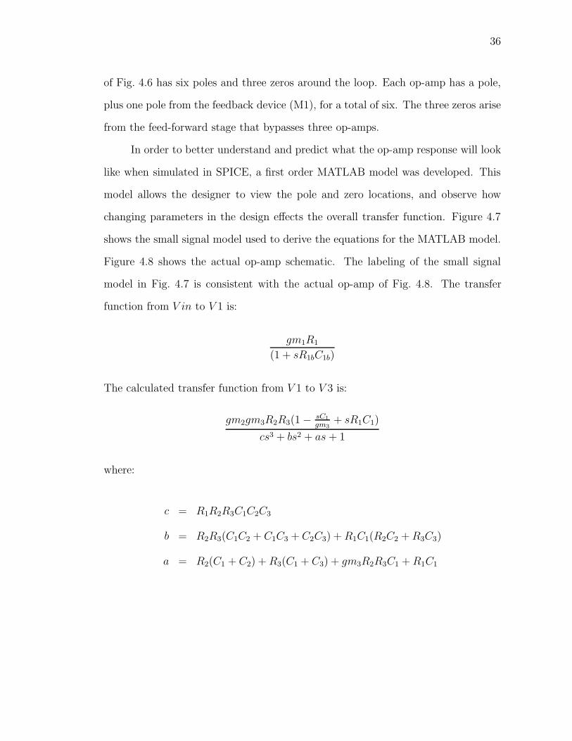
36
of Fig. 4.6 has six poles and three zeros around the loop. Each op-amp has a pole,
plus one pole from the feedback device (M1), for a total of six. The three zeros arise
from the feed-forward stage that bypasses three op-amps.
In order to better understand and predict what the op-amp response will look
like when simulated in SPICE, a first order MATLAB model was developed. This
model allows the designer to view the pole and zero locations, and observe how
changing parameters in the design effects the overall transfer function. Figure 4.7
shows the small signal model used to derive the equations for the MATLAB model.
Figure 4.8 shows the actual op-amp schematic. The labeling of the small signal
model in Fig. 4.7 is consistent with the actual op-amp of Fig. 4.8. The transfer
function from V in to V 1 is:
gm1R1
(1 + sR1bC1b)
The calculated transfer function from V 1 to V 3 is:
gm2gm3R2R3(1− sC1
gm3+ sR1C1)
cs3 + bs2 + as + 1
where:
c = R1R2R3C1C2C3
b = R2R3(C1C2 + C1C3 + C2C3) +R1C1(R2C2 +R3C3)
a = R2(C1 + C2) +R3(C1 + C3) + gm3R2R3C1 +R1C1
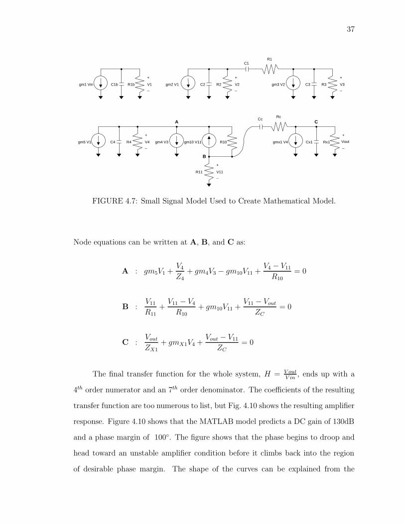
37
R1bC1bgm1 Vin
+
_V1 R2C2gm2 V1
+
_V2 R3C3gm3 V2
+
_V3
R1C1
VoutR4C4gm5 V1
+
_V4 gm4 V3 gm10 V11 R10
R11
+
_V11
Rx1Cx1gmx1 V4
+
_
RcCc
A
B
C
FIGURE 4.7: Small Signal Model Used to Create Mathematical Model.
Node equations can be written at A, B, and C as:
A : gm5V1 +V4
Z4
+ gm4V3 − gm10V11 +V4 − V11
R10
= 0
B :V11
R11+V11 − V4
R10+ gm10V11 +
V11 − VoutZC
= 0
C :VoutZX1
+ gmX1V4 +Vout − V11
ZC= 0
The final transfer function for the whole system, H = V outV in
, ends up with a
4th order numerator and an 7th order denominator. The coefficients of the resulting
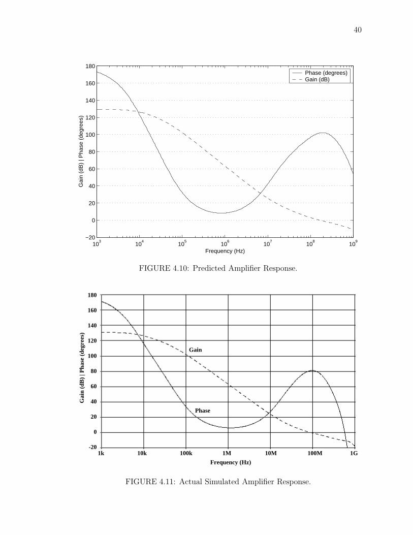
transfer function are too numerous to list, but Fig. 4.10 shows the resulting amplifier
response. Figure 4.10 shows that the MATLAB model predicts a DC gain of 130dB
and a phase margin of 100◦. The figure shows that the phase begins to droop and
head toward an unstable amplifier condition before it climbs back into the region
of desirable phase margin. The shape of the curves can be explained from the
38
VrefCcRc
DACM6 M7 M8 M9 M11
M10
M5M4M3M2
M13M12
M1a M1b
Mx1
C1Vref
FIGURE 4.8: Feed-Forward Amplifier Schematic.
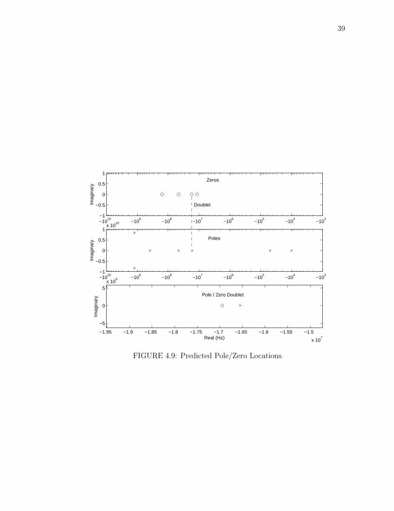
pole/zero plot of Fig. 4.9. Figure 4.9 shows that as the frequency increases, the
signal originally sees two poles before the zeros begin to enter and correct the phase
of the transfer function. The right-half-plane zero that would normally be present
because of the miller capacitor C1 is moved to the left half plane due to a larger
left-half-plane zero created by the feed-forward stage.
Figure 4.9 also shows a zoomed in view of a pole/zero doublet. This doublet
is created as a zero from the feed-forward device is placed very close to one of the
poles from the low frequency stages. It is unclear exactly how the presence of the
pole/zero doublet effects the settling time [24, 25], but it is known that the presence
of a pole/zero doublet does degrade the settling time. SPICE simulations show that
the op-amp still settles to within 0.01% in 25 ns, making it more than adequate for
the DC application.
4.4 Simulation Results
The amplifier design of Fig. 4.8 was designed and simulated using SPICE
after making initial parameter settings with the MATLAB model. As was previ-
39
−1010
−109
−108
−107
−106
−105
−104
−103
−1
−0.5
0
0.5
1
Imag
inar
y
−1010
−109
−108
−107
−106
−105
−104
−103
−1
−0.5
0
0.5
1x 10
10
Imag
inar
y
−1.95 −1.9 −1.85 −1.8 −1.75 −1.7 −1.65 −1.6 −1.55 −1.5
x 107
−5
0
5x 10
8
Real (Hz)
Imag
inar
y
Zeros
Poles
Pole / Zero Doublet
Doublet
FIGURE 4.9: Predicted Pole/Zero Locations.
40
103
104
105
106
107
108
109
−20
0
20
40
60
80
100
120
140
160
180
Frequency (Hz)
Gai
n (d
B)
| Pha
se (
degr
ees)
Phase (degrees)Gain (dB)
FIGURE 4.10: Predicted Amplifier Response.
Gain
Phase
1k 10k 100k 1M 10M 100M 1G-20
0
20
40
60
80
100
120
140
160
180
Gai
n (d
B)
| Pha
se (
degr
ees)
Frequency (Hz)
FIGURE 4.11: Actual Simulated Amplifier Response.
41
ously mentioned, the amplifier was simulated for loop characteristics, and therefore
Fig. 4.8 shows the feed-back device Mx1 in the schematic. Figure 4.11 shows the
actual loop response when simulated in SPICE. The DC gain exactly matches the
MATLAB model prediction of Fig. 4.10. Both of the curves (gain and phase) match
the predicted response of Fig. 4.10 extremely well. One anticipated difference is the
phase response above 20 MHz. The model predicted 100◦ phase margin, while the
actual simulations show that the phase margin is really 80◦. The 100◦ prediction
made by the model only accounts for first order poles in the system and does not
correctly model the higher order poles which create the actual phase response seen
in Fig. 4.11.
42
5. IMPLEMENTATION
Considering the process and temperature variations of the device parameters,
a 10-Bit DAC was designed and implemented in TSMC’s digital 0.18 µm CMOS
process. This process has a single-poly layer and 5 metal layers. The fabricated chip
was packaged in a 52-pin PLCC package. The design was simulated in SPICE and
modeled effectively in MATLAB before fabrication. Extensive area optimization
was done to minimize the die space required for the layout. Recall that Fig. 3.2
shows the schematic of the final DAC core. The implemented chip includes all the
digital circuitry and the linear output circuit discussed earlier.
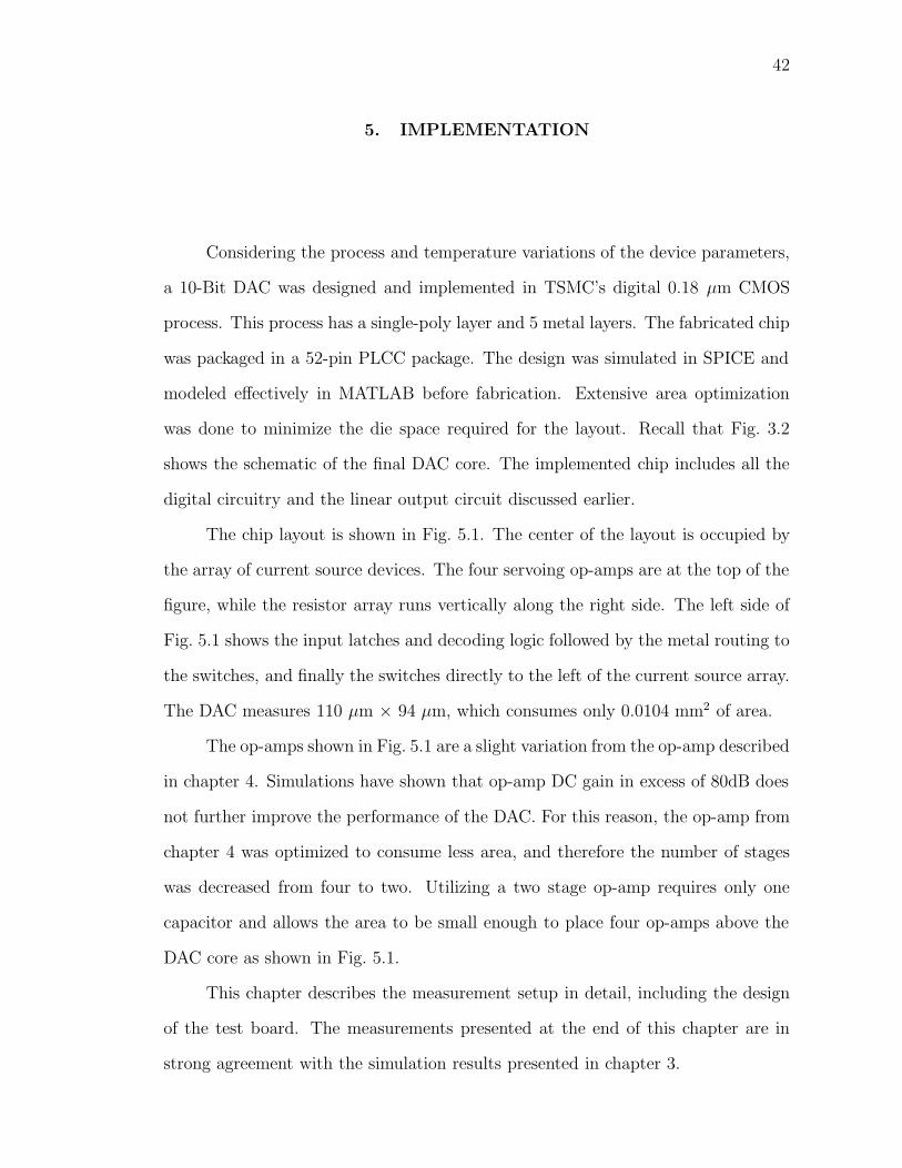
The chip layout is shown in Fig. 5.1. The center of the layout is occupied by
the array of current source devices. The four servoing op-amps are at the top of the
figure, while the resistor array runs vertically along the right side. The left side of
Fig. 5.1 shows the input latches and decoding logic followed by the metal routing to
the switches, and finally the switches directly to the left of the current source array.
The DAC measures 110 µm × 94 µm, which consumes only 0.0104 mm2 of area.
The op-amps shown in Fig. 5.1 are a slight variation from the op-amp described
in chapter 4. Simulations have shown that op-amp DC gain in excess of 80dB does
not further improve the performance of the DAC. For this reason, the op-amp from
chapter 4 was optimized to consume less area, and therefore the number of stages
was decreased from four to two. Utilizing a two stage op-amp requires only one
capacitor and allows the area to be small enough to place four op-amps above the
DAC core as shown in Fig. 5.1.
This chapter describes the measurement setup in detail, including the design
of the test board. The measurements presented at the end of this chapter are in
strong agreement with the simulation results presented in chapter 3.
43
FIGURE 5.1: 10-Bit DAC Layout.
44
474849505152123456746
45
44
43
42
41
40
39
38
37
36
35
3433323130292827262524232221
9
10
11
12
13
14
15
16
17
18
19
20
8
DAC
VDDVDD
D0
D1
D2
D3
D4
D5
D6
D7
D8
D9
NA
VDD VDD
EN
Vref
Ibias
Vbias
NA
NA
NA
NA
NA
NA
NA
NA
NA
Ioutp_S1
Ioutn_S1
Ioutp_S2
Ioutn_S2
Ioutp_NS1
Ioutn_NS1
Ioutp_NS2
Ioutn_NS2
NA
NA
NA
NA
NA
NA
NA
NA
NA
NA
COUNTER
DIP
SWITCHES
+5V
ProgrammableInputs
D0:D11
+5V
BUFFER
VDD
+5V
NC
S
R
Q
Q
+5V
External Clock
DIP
SWITCHES
VDD
DO:D9DO:D9
DO:D9SMA
50k
50k
+5V
0-25k
10k
Vref
vin
vout
gnd
n/c
n/c
n/c
n/c
n/c
MC1403UDS
0.1 uF
Vbias
0-25k
10kvin
vout
gnd
n/c
n/c
n/c
n/c
n/c
MC1403UDS
+5V
0.1 uF
FIGURE 5.2: DAC Test Board.
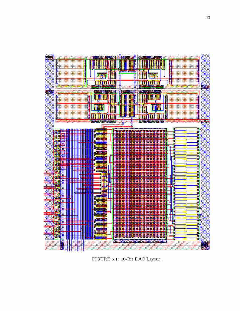
5.1 Measurement Setup
In order to measure the performance of the DAC with accuracy and repeata-
bility, a test board was designed and fabricated for testing the chip. A functional
diagram of the test board is shown in Fig. 5.2. Figure 5.2 shows that the input to
the DAC can either be controlled manually by selecting the appropriate code with
a set of DIP switches or by a binary counter. The binary counter advances to the
next binary code with every clock pulse that it receives. This clock can be manually
controlled with a switch, or driven externally from an outside source. Figure 5.2
also shows some precision voltage reference chips used to develop the needed bias
voltages and current.
45
POWER SUPPLY
TEST BOARDHIGH PRECISION
DIGITAL MULTIMETER(DMM)
PC WITH GPIB CARDAND LABVIEW
GPIB
COUNTERADVANCE
OUTPUT
POWER
FIGURE 5.3: DAC Measurement Setup.
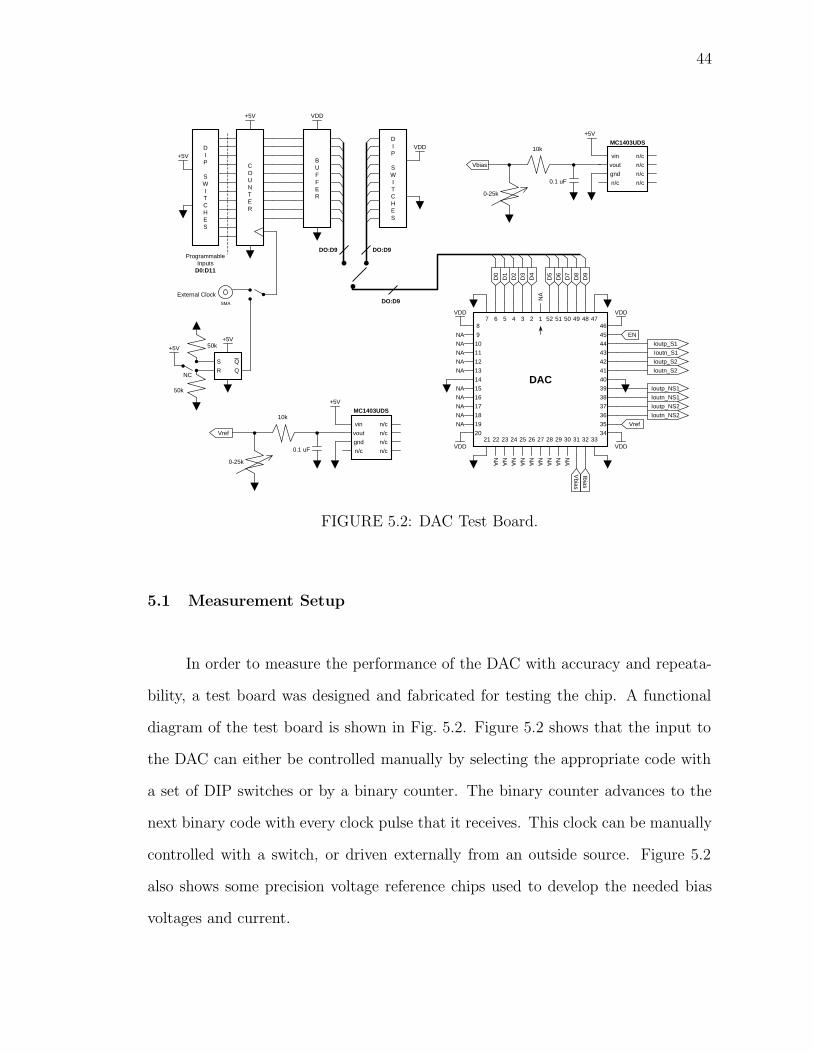
The measurement setup has been automated with the help of LabView and
the appropriate GPIB test equipment. Figure 5.3 shows a functional diagram of
the measurement setup. The figure shows a high precision DMM connected to the
output of the DAC to measure the analog voltages at the output. This DMM is
connected to a PC via a GPIB interface. The GPIB interface allows the computer
to capture all the data from the DMM and store it in a file, or make mathematical
calculations on the data. LabView is the software program used on the PC to
interface with the DMM and capture the data. A single pin on the parallel port of
the PC is used to advance the binary counter to the next code once all the data for
a particular code has been captured. This process repeats itself until all 1024 input
codes have been tested. The automated testing allows for easy and reliable testing
over the entire lot of sample chips.
46
5.2 Experimental Results
Measurements were taken on ten different DACs provided upon fabrication.
Using the measurement setup described earlier, LabView was used to capture 100
analog output data points for every input code. These data points were averaged
for each input code, resulting in only one analog output per input code. Figure 5.4
shows the analog output as a function of input code. The data used to create
Fig. 5.4 was measured using the differential output of the DAC. Figure 5.5 shows
the best case measured INL and DNL for the 10-Bit DAC with the linear output
current mirror described in chapter 3. Figure 5.5 shows that the INL is nearly 1
LSB peak-peak which means that this DAC is almost truly 10-Bit linear. The DNL
plot of Fig. 5.5 shows that the DAC is 10-Bit monotonic.
The fact that the DAC measures 10-Bit monotonicity is the most impressive
statistic since the original goal was to achieve 10-Bit monotonicity regardless of the
linearity. As was mentioned in chapter 2, the DAC is monotonic if the DNL is greater
than -1 LSB. Figure 5.5 shows the minimum DNL for the best case DAC tested is
-0.263 LSB which is much greater than the -1 LSB minimum needed to maintain
monotonicity. Even the common error transition from input code 0111111111 to
1000000000 does not have a large DNL spike. This transition is commonly referred
to as the MSB transition, and is a common location for DNL errors in segmented
architectures. The reason for the error at this particular transition is due to the
fact that it is the largest number of currents being turned off, with only one current
being turned on in its place over the entire input code range. A good DNL at this
transition requires that the MSB current source be 1 LSB greater than the sum
of all the other current sources in the DAC. Since every current source has some
random variation, it is very difficult to match the MSB current source to the sum of
many current sources; each of which contain a certain amount of random variation.
47
0 100 200 300 400 500 600 700 800 900 1000−0.8
−0.6
−0.4
−0.2
0
0.2
0.4
0.6
0.8
Input Code
Diff
eren
tial O
utpu
t Vol
tage
(V
olts
)
FIGURE 5.4: Measured DAC Transfer Curve.
0 100 200 300 400 500 600 700 800 900 1000−1
−0.5
0
0.5
1INL
INL
(LS
B)
0 100 200 300 400 500 600 700 800 900 1000−1
−0.5
0
0.5
1DNL
DN
L (L
SB
)
Input Code
FIGURE 5.5: Best Case Measured INL and DNL Performance.
48
0 100 200 300 400 500 600 700 800 900 1000−1.5
−1
−0.5
0
0.5
1
1.5INL
INL
(LS
B)
0 100 200 300 400 500 600 700 800 900 1000−1.5
−1
−0.5
0
0.5
1
1.5DNL
DN
L (L
SB
)
Input Code
FIGURE 5.6: Worst Case Measured INL and DNL Performance.
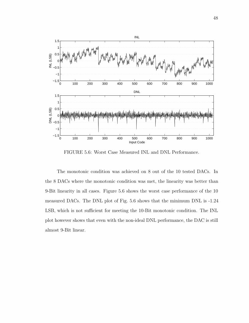
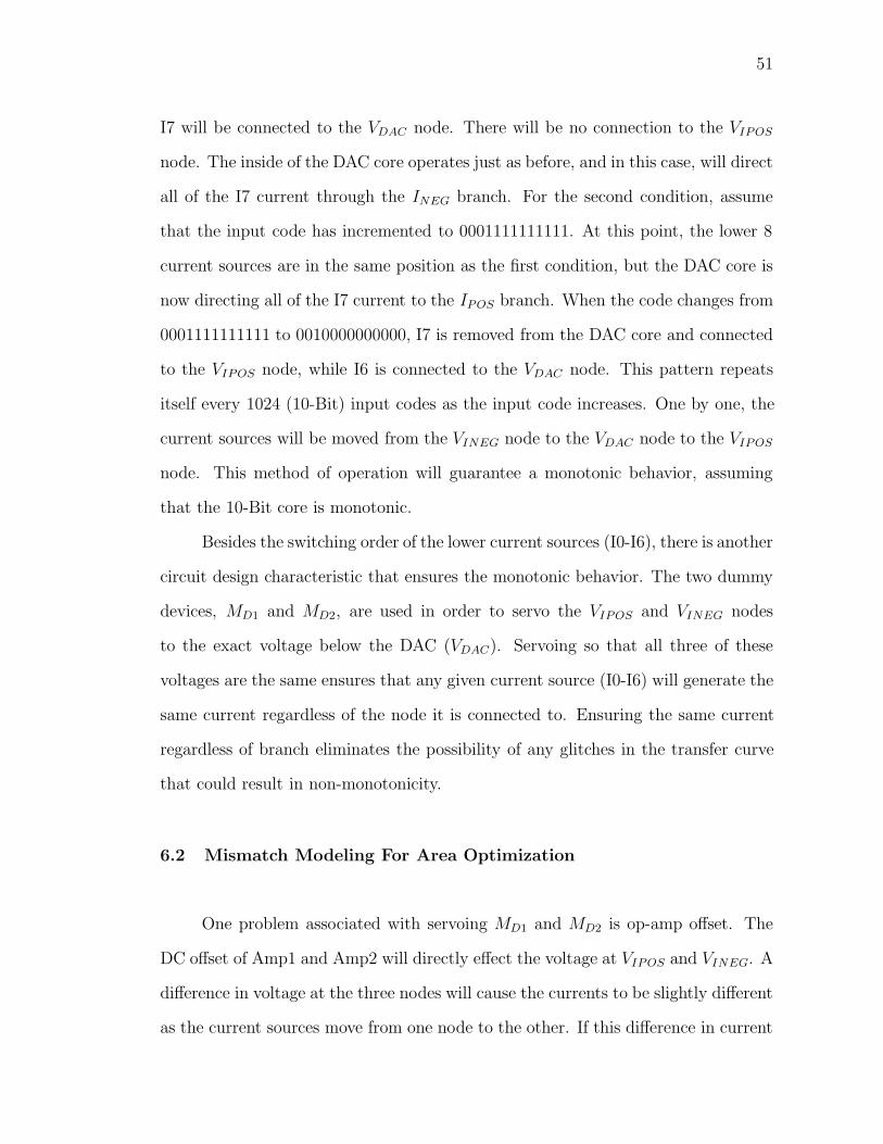
The monotonic condition was achieved on 8 out of the 10 tested DACs. In
the 8 DACs where the monotonic condition was met, the linearity was better than
9-Bit linearity in all cases. Figure 5.6 shows the worst case performance of the 10
measured DACs. The DNL plot of Fig. 5.6 shows that the minimum DNL is -1.24
LSB, which is not sufficient for meeting the 10-Bit monotonic condition. The INL
plot however shows that even with the non-ideal DNL performance, the DAC is still
almost 9-Bit linear.
49
6. HIGHER RESOLUTION DAC DESIGN
While the 10-Bit DAC described in chapter 3 is suitable for most DC appli-
cations, there are instances where a DC DAC with a higher resolution than 10-Bits
is required. Just as with the 10-Bit case, area consumption is of prime concern in
this higher order DAC design. This chapter introduces a 13-Bit DC DAC design
that utilizes the already high-accuracy 10-Bit core for minimal area consumption.
The DAC architecture adds a minimal number of devices around the existing 10-
Bit DAC to guarantee a monotonic behavior. The optimization of die area that
resulted in the chosen device sizes is discussed in detail. The analysis of op-amp
offset and current source device mismatch using SPICE will be examined before the
final simulation results are presented.
6.1 Architecture Design
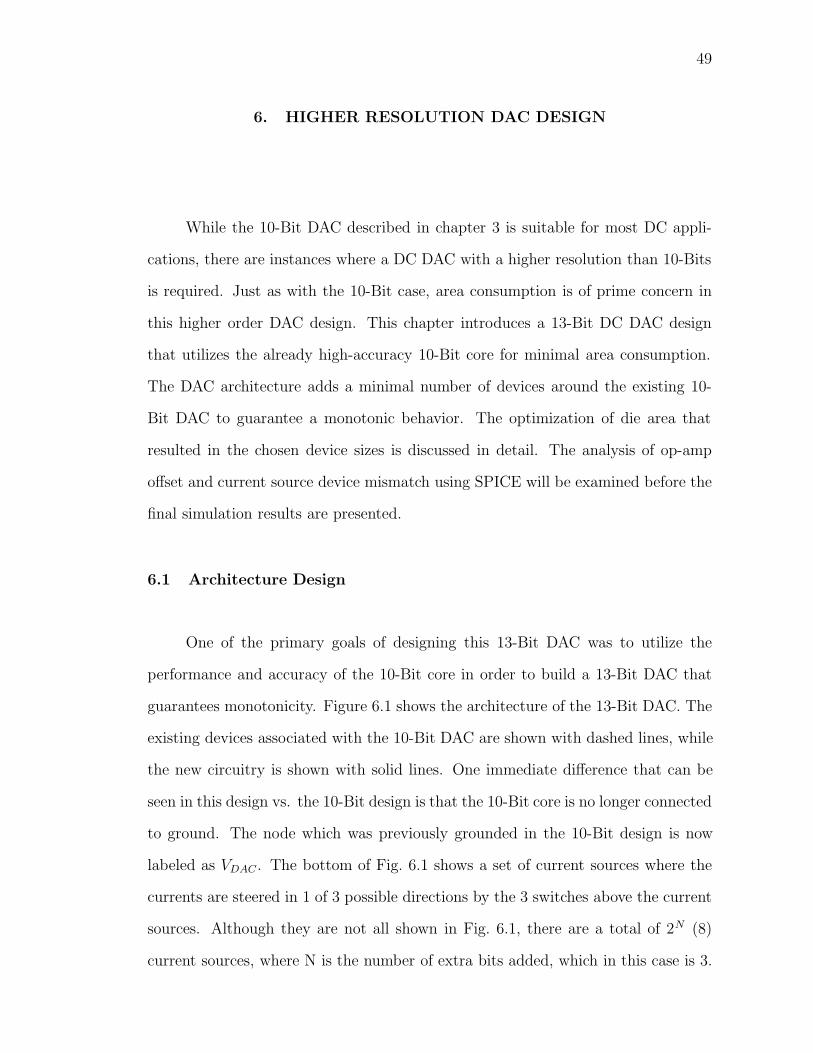
One of the primary goals of designing this 13-Bit DAC was to utilize the
performance and accuracy of the 10-Bit core in order to build a 13-Bit DAC that
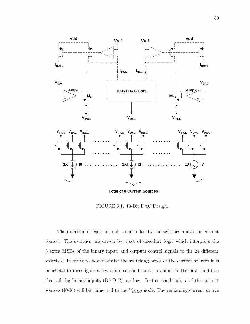
guarantees monotonicity. Figure 6.1 shows the architecture of the 13-Bit DAC. The
existing devices associated with the 10-Bit DAC are shown with dashed lines, while
the new circuitry is shown with solid lines. One immediate difference that can be
seen in this design vs. the 10-Bit design is that the 10-Bit core is no longer connected
to ground. The node which was previously grounded in the 10-Bit design is now
labeled as VDAC . The bottom of Fig. 6.1 shows a set of current sources where the
currents are steered in 1 of 3 possible directions by the 3 switches above the current
sources. Although they are not all shown in Fig. 6.1, there are a total of 2N (8)
current sources, where N is the number of extra bits added, which in this case is 3.
50
1X 1X1X
+
_
VDAC
+
_
+
_
IOUT2
VddVref
+
_
IOUT1
VrefVdd
VDAC
VDAC VINEGVIPOS
VINEG VINEG VINEGVDAC VDAC VDACVIPOSVIPOSVIPOS
10-Bit DAC Core
Total of 8 Current Sources
Amp1 Amp2
MD1 MD2
I0 I3 I7
IPOS INEG
…………. ………….
…….
…….
…….
…….
FIGURE 6.1: 13-Bit DAC Design.
The direction of each current is controlled by the switches above the current
source. The switches are driven by a set of decoding logic which interprets the
3 extra MSBs of the binary input, and outputs control signals to the 24 different
switches. In order to best describe the switching order of the current sources it is
beneficial to investigate a few example conditions. Assume for the first condition
that all the binary inputs (D0-D12) are low. In this condition, 7 of the current
sources (I0-I6) will be connected to the VINEG node. The remaining current source
51
I7 will be connected to the VDAC node. There will be no connection to the VIPOS
node. The inside of the DAC core operates just as before, and in this case, will direct
all of the I7 current through the INEG branch. For the second condition, assume
that the input code has incremented to 0001111111111. At this point, the lower 8
current sources are in the same position as the first condition, but the DAC core is
now directing all of the I7 current to the IPOS branch. When the code changes from
0001111111111 to 0010000000000, I7 is removed from the DAC core and connected
to the VIPOS node, while I6 is connected to the VDAC node. This pattern repeats
itself every 1024 (10-Bit) input codes as the input code increases. One by one, the
current sources will be moved from the VINEG node to the VDAC node to the VIPOS
node. This method of operation will guarantee a monotonic behavior, assuming
that the 10-Bit core is monotonic.
Besides the switching order of the lower current sources (I0-I6), there is another
circuit design characteristic that ensures the monotonic behavior. The two dummy
devices, MD1 and MD2, are used in order to servo the VIPOS and VINEG nodes
to the exact voltage below the DAC (VDAC). Servoing so that all three of these
voltages are the same ensures that any given current source (I0-I6) will generate the
same current regardless of the node it is connected to. Ensuring the same current
regardless of branch eliminates the possibility of any glitches in the transfer curve
that could result in non-monotonicity.
6.2 Mismatch Modeling For Area Optimization
One problem associated with servoing MD1 and MD2 is op-amp offset. The
DC offset of Amp1 and Amp2 will directly effect the voltage at VIPOS and VINEG. A
difference in voltage at the three nodes will cause the currents to be slightly different
as the current sources move from one node to the other. If this difference in current
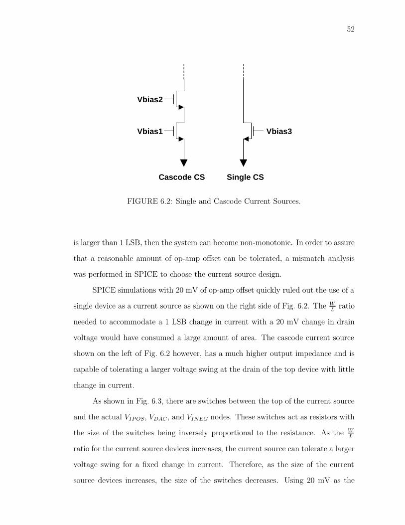
52
Cascode CS Single CS
Vbias3Vbias1
Vbias2
FIGURE 6.2: Single and Cascode Current Sources.
is larger than 1 LSB, then the system can become non-monotonic. In order to assure
that a reasonable amount of op-amp offset can be tolerated, a mismatch analysis
was performed in SPICE to choose the current source design.
SPICE simulations with 20 mV of op-amp offset quickly ruled out the use of a
single device as a current source as shown on the right side of Fig. 6.2. The WL
ratio
needed to accommodate a 1 LSB change in current with a 20 mV change in drain
voltage would have consumed a large amount of area. The cascode current source
shown on the left of Fig. 6.2 however, has a much higher output impedance and is
capable of tolerating a larger voltage swing at the drain of the top device with little
change in current.
As shown in Fig. 6.3, there are switches between the top of the current source
and the actual VIPOS, VDAC , and VINEG nodes. These switches act as resistors with
the size of the switches being inversely proportional to the resistance. As the WL
ratio for the current source devices increases, the current source can tolerate a larger
voltage swing for a fixed change in current. Therefore, as the size of the current
source devices increases, the size of the switches decreases. Using 20 mV as the
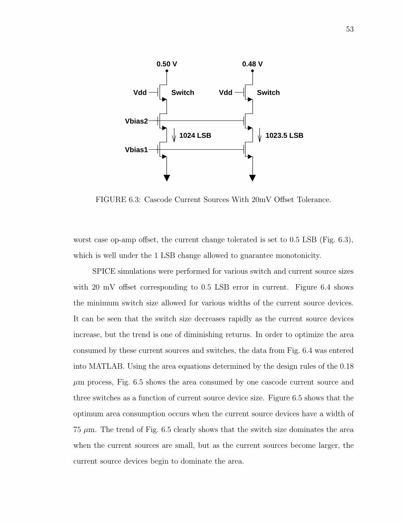
53
Vbias1
Vbias2
Vdd Vdd
0.50 V 0.48 V
1023.5 LSB1024 LSB
SwitchSwitch
FIGURE 6.3: Cascode Current Sources With 20mV Offset Tolerance.
worst case op-amp offset, the current change tolerated is set to 0.5 LSB (Fig. 6.3),
which is well under the 1 LSB change allowed to guarantee monotonicity.
SPICE simulations were performed for various switch and current source sizes
with 20 mV offset corresponding to 0.5 LSB error in current. Figure 6.4 shows
the minimum switch size allowed for various widths of the current source devices.
It can be seen that the switch size decreases rapidly as the current source devices
increase, but the trend is one of diminishing returns. In order to optimize the area
consumed by these current sources and switches, the data from Fig. 6.4 was entered
into MATLAB. Using the area equations determined by the design rules of the 0.18
µm process, Fig. 6.5 shows the area consumed by one cascode current source and
three switches as a function of current source device size. Figure 6.5 shows that the
optimum area consumption occurs when the current source devices have a width of
75 µm. The trend of Fig. 6.5 clearly shows that the switch size dominates the area
when the current sources are small, but as the current sources become larger, the
current source devices begin to dominate the area.
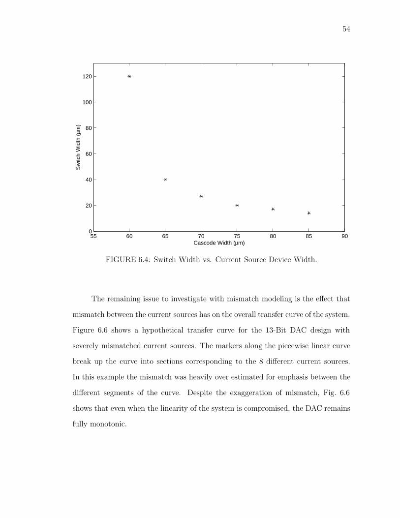
54
55 60 65 70 75 80 85 900
20
40
60
80
100
120
Cascode Width (µm)
Sw
itch
Wid
th (µ
m)
FIGURE 6.4: Switch Width vs. Current Source Device Width.
The remaining issue to investigate with mismatch modeling is the effect that
mismatch between the current sources has on the overall transfer curve of the system.
Figure 6.6 shows a hypothetical transfer curve for the 13-Bit DAC design with
severely mismatched current sources. The markers along the piecewise linear curve
break up the curve into sections corresponding to the 8 different current sources.
In this example the mismatch was heavily over estimated for emphasis between the
different segments of the curve. Despite the exaggeration of mismatch, Fig. 6.6
shows that even when the linearity of the system is compromised, the DAC remains
fully monotonic.
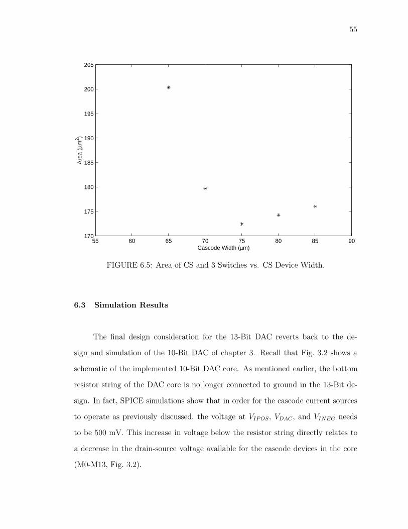
55
55 60 65 70 75 80 85 90170
175
180
185
190
195
200
205
Cascode Width (µm)
Are
a (µ
m2 )
FIGURE 6.5: Area of CS and 3 Switches vs. CS Device Width.
6.3 Simulation Results
The final design consideration for the 13-Bit DAC reverts back to the de-
sign and simulation of the 10-Bit DAC of chapter 3. Recall that Fig. 3.2 shows a
schematic of the implemented 10-Bit DAC core. As mentioned earlier, the bottom
resistor string of the DAC core is no longer connected to ground in the 13-Bit de-
sign. In fact, SPICE simulations show that in order for the cascode current sources
to operate as previously discussed, the voltage at VIPOS, VDAC , and VINEG needs
to be 500 mV. This increase in voltage below the resistor string directly relates to
a decrease in the drain-source voltage available for the cascode devices in the core
(M0-M13, Fig. 3.2).
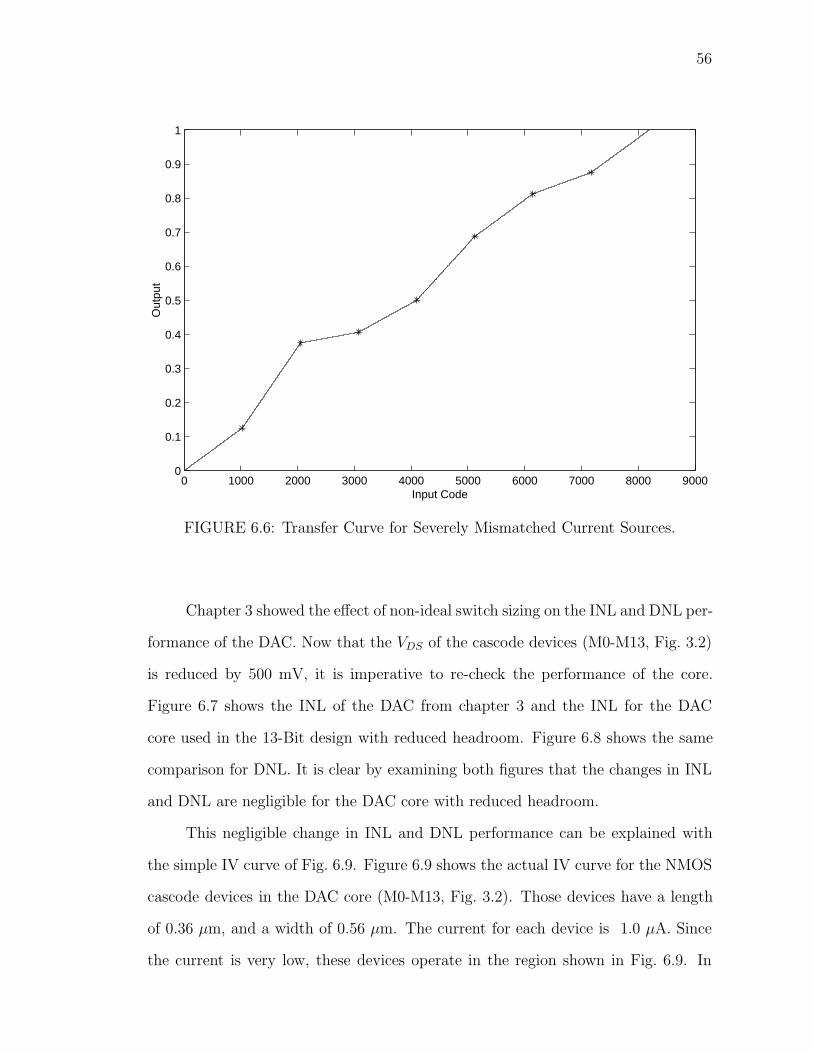
56
0 1000 2000 3000 4000 5000 6000 7000 8000 90000
0.1
0.2
0.3
0.4
0.5
0.6
0.7
0.8
0.9
1
Input Code
Out
put
FIGURE 6.6: Transfer Curve for Severely Mismatched Current Sources.
Chapter 3 showed the effect of non-ideal switch sizing on the INL and DNL per-
formance of the DAC. Now that the VDS of the cascode devices (M0-M13, Fig. 3.2)
is reduced by 500 mV, it is imperative to re-check the performance of the core.
Figure 6.7 shows the INL of the DAC from chapter 3 and the INL for the DAC
core used in the 13-Bit design with reduced headroom. Figure 6.8 shows the same
comparison for DNL. It is clear by examining both figures that the changes in INL
and DNL are negligible for the DAC core with reduced headroom.
This negligible change in INL and DNL performance can be explained with
the simple IV curve of Fig. 6.9. Figure 6.9 shows the actual IV curve for the NMOS
cascode devices in the DAC core (M0-M13, Fig. 3.2). Those devices have a length
of 0.36 µm, and a width of 0.56 µm. The current for each device is 1.0 µA. Since
the current is very low, these devices operate in the region shown in Fig. 6.9. In
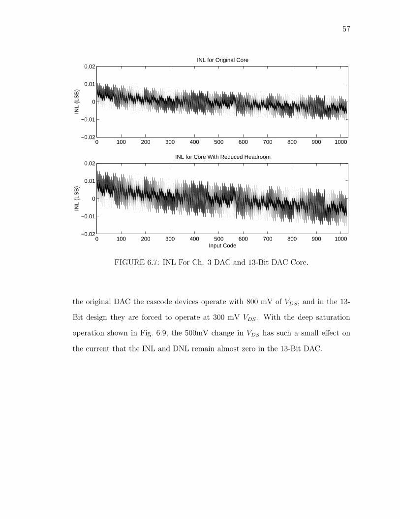
57
0 100 200 300 400 500 600 700 800 900 1000−0.02
−0.01
0
0.01
0.02INL for Original Core
INL
(LS
B)
0 100 200 300 400 500 600 700 800 900 1000−0.02
−0.01
0
0.01
0.02INL for Core With Reduced Headroom
INL
(LS
B)
Input Code
FIGURE 6.7: INL For Ch. 3 DAC and 13-Bit DAC Core.
the original DAC the cascode devices operate with 800 mV of VDS, and in the 13-
Bit design they are forced to operate at 300 mV VDS. With the deep saturation
operation shown in Fig. 6.9, the 500mV change in VDS has such a small effect on
the current that the INL and DNL remain almost zero in the 13-Bit DAC.
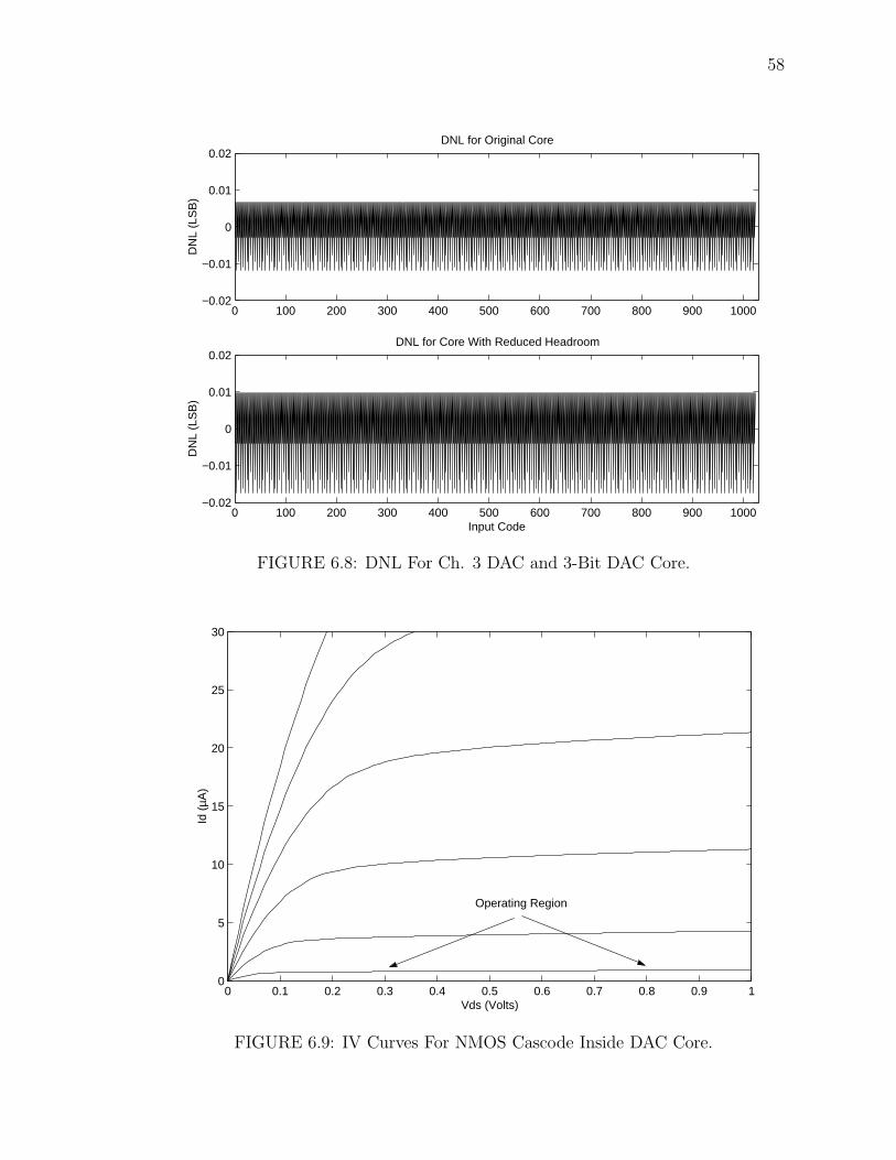
58
0 100 200 300 400 500 600 700 800 900 1000−0.02
−0.01
0
0.01
0.02DNL for Original Core
DN
L (L
SB
)
0 100 200 300 400 500 600 700 800 900 1000−0.02
−0.01
0
0.01
0.02DNL for Core With Reduced Headroom
DN
L (L
SB
)
Input Code
FIGURE 6.8: DNL For Ch. 3 DAC and 3-Bit DAC Core.
0 0.1 0.2 0.3 0.4 0.5 0.6 0.7 0.8 0.9 10
5
10
15
20
25
30
Vds (Volts)
Id (
µA)
Operating Region
FIGURE 6.9: IV Curves For NMOS Cascode Inside DAC Core.
59
7. CONCLUSIONS
The key factor driving the design of the low voltage DC DACs presented in
this thesis is area optimization and minimization. No previous CMOS DACs have
been published that show static performance at the 10-Bit level with a die size as
small as what was presented. A brief summary of the thoughts and ideas presented
in this work is given followed by a short discussion on future work that can be done
in this area.
7.1 Summary
This thesis describes the design, modeling, and implementation of two area
efficient highly accurate DC DACs. The presented 10-Bit DAC uses the performance
advantages of thermometer coding on the 3 most significant bits, while maximizing
performance and minimizing area with a R-2R ladder for the least significant bits.
An ultra high gain servoing technique was used to overcome the limitations of the
1.8V power supply. This technique was used to design a linear current mirror with
1 V of available headroom at the output.
An advanced MATLAB model was presented that analyzed the branch cur-
rents in various DAC designs, and allowed for a side-by-side comparison of architec-
tures. This model was used to assign random device mismatch and observe which
architectures showed the best performance. The MATLAB model showed the dras-
tic improvement in performance with a resistor based design over a standard current
steering design without resistors for the given mismatch parameters.
A five stage, ultra high gain op-amp with feed-forward parallel path compen-
sation was presented for servoing. The op-amp has a loop gain of 130 dB and a
60
loop phase margin of 81◦. The feed-forward op-amp was extensively modeled with
MATLAB to produce pole/zero locations and accurately predict the AC response.
The model allowed for a complete analysis of the op-amp response to variations in
device parameters.
The 10-Bit DAC described in chapter 3 was fabricated in a standard digital,
0.18 µm CMOS process. Special attention was given to the layout to minimize the
effects of process and temperature gradients. MATLAB and SPICE modeling lead
to an accurate DC DAC which has been optimized for area. The layout measures
110 µm × 94 µm, and consumes 0.0104 mm2 of area. The measured results show ex-
tremely promising figures for such a compact and efficient DAC. The measurements
correlate very well with the simulated results presented. The maximum measured
INL is 1.65 LSBs and the maximum measured DNL is -0.95 LSBs; proving that the
fabricated DAC is 10-Bit monotonic.
7.2 Future Research
New theories and ideas are constantly surfacing which attempt to improve the
performance of mixed-signal ICs. Improvements in continuous time op-amp offset
cancellation could be applied directly to the designs presented in this work. An
area efficient method for canceling offsets in the servoing op-amps would improve
the performance of the output current mirror. In addition, canceling the offset in
the servo op-amps added in the 13-Bit design would eliminate the need for a cascode
current source. Using a single device current source would allow the 10-Bit core to
have more headroom while operating in the 13-Bit design, and hence would improve
its performance. Modeling of the 13-Bit design could be extended into MATLAB
the same way the 10-Bit design was. Additional MATLAB modeling of the 10-Bit
design could also include the second order effects of the cascode current sources, and

61
the non-linear resistance created by the switches. And finally, the size of the current
source array in the DAC could be extended to achieve better matching, or the DAC
could be implemented in a different process where the matching characteristics are
more accurately controlled.
62
REFERENCES
1. S.-Y. Chin and C.-Y. Wu, “A 10-b 125-MHz CMOS Digital-to-Analog Con-verter with threshold voltage compensated current sources,” IEEE J. SolidState Circuits, vol. 29, pp. 1374–1380, November 1994.
2. A. V. den Bosch, M. Borremans, M. Steyaert, and W. Sansen, “A 10-bit 1-GS/snyquist current-steering CMOS D/A converter,” IEEE J. Solid State Circuits,vol. 36, pp. 315–324, March 2001.
3. C. Hammerschmied and Q. Huang, “Design and implementation of anuntrimmed MOSFET-only 10-bit A/D converter with -79-dB THD,” IEEEJ. Solid State Circuits, vol. 33, pp. 1148–1157, August 1998.
4. B. Greenley, U.-K. Moon, and R. Veith, “A 1.8 V CMOS DAC cell with ultrahigh gain op-amp in 0.0143 mm2,” Proc. of the IEEE International Symposiumon Circuits and Systems, May 2001.
5. C.-H. Lin and K. Bult, “A 10-b, 500-MSample/s CMOS DAC in 0.6 mm2,”IEEE J. Solid State Circuits, vol. 33, pp. 1948–1958, December 1998.
6. K. Bult and G. Geelen, “An inherently linear and compact MOST-only cur-rent division technique,” IEEE J. Solid State Circuits, vol. 27, pp. 1730–1735,December 1992.
7. M. Borgatti, A. Rocchi, M. Bisio, M. Besana, L. Navoni, and P. Rolandi, “A 64-Min single-chip voice recorder/player using embedded 4-b/cell flash memory,”IEEE J. Solid State Circuits, vol. 36, pp. 516–521, March 2001.
8. A. Rofougaran, G. Chang, J. Rael, J.-C. Chang, M. Rofougaran, P. Chang,M. Djafari, J. Min, E. Roth, A. Abidi, and H. Samueli, “A single-chip 900-MHz spread spectrum wireless transceiver in 1-µm CMOS part II: receiverdesign,” IEEE J. Solid State Circuits, vol. 33, pp. 535–547, April 1998.
9. T. Cho, E. Dukatz, M. Mack, D. Macnally, M. Marringa, S. Mehta, C. Nilson,L. Plouvier, and S. Rabii, “A single-chip CMOS direct-conversion transceiverfor 900-MHz spread spectrum digital cordless phones,” Proc. of the IEEE In-ternational Solid-State Circuits Conference, pp. 228–229, February 1999.
10. D. Seo, A. Weil, and M. Feng, “A 14Bit, 1 GS/s digital-to-analog converter withimproved dynamic performances,” Proc. of the IEEE International Symposiumon Circuits and Systems, pp. V541–V544, May 2000.
11. J. Bastos, A. Marques, M. Steyaert, and W. Sansen, “A 12-Bit intrinsic accu-racy high-speed CMOS DAC,” IEEE J. Solid State Circuits, vol. 33, pp. 1959–1969, December 1998.
63
12. A. V. den Bosch, M. Steyaert, and W. Sansen, “The extraction of transistormismatch parameters: the CMOS current steering D/A converter as a teststructure,” Proc. of the IEEE International Symposium on Circuits and Sys-tems, pp. II745–II748, May 2000.
13. V. Cheung, H. Luong, and W. Ki, “A 1-V CMOS switched-opamp switched ca-pacitor pseudo-2-path filter,” IEEE J. Solid State Circuits, pp. 14–22, January2001.
14. M. Dessouky and A. Kaiser, “Very low-voltage digital-audio ∆Σ modulatorwith 88-dB dynamic range using local switch bootstrapping,” IEEE J. SolidState Circuits, pp. 349–355, March 2001.
15. D. A. Johns and K. Martin, Analog Integrated Circuit Design. New York, NY:John Wiley & Sons, Inc., 1997.
16. B. Razavi, Principles of Data Conversion System Design. New York, NY:IEEE Press, 1999.
17. S. Norsworthy, R. Schreier, and G. Temes, Delta-Sigma Data Converters: The-ory, Design, and Simulation. New York, NY: IEEE Press, 1997.
18. D. Mercer, “A 16-b D/A converter with increased spurious free dynamic range,”IEEE J. Solid State Circuits, vol. 29, pp. 1180–1185, October 1994.
19. A. V. den Bosch, M. Borremans, M. Stayeart, and W. Sansen, “A 12b500MSample/s current-steering CMOS D/A converter,” Proc. of the IEEE In-ternational Solid-State Circuits Conference, pp. 366–367, February 2001.
20. G. V. der Plas, J. Vandenbussche, W. Sansen, M. Steyaert, and G. Gielen, “A14-bit intrinsic accuracy Q2 random walk CMOS DAC,” IEEE J. Solid StateCircuits, vol. 34, pp. 1708–1718, December 1999.
21. A. Bugeja, B.-S. Song, P. Rakers, and S. Gillig, “A 14-b, 100-MS/s CMOSDAC designed for spectral performance,” IEEE J. Solid State Circuits, vol. 34,pp. 1719–1731, December 1999.
22. A. Thomsen, D. Kasha, L. Wang, and W. Lee, “A 110-dB-THD, 18mW DACusing sampling of the output and feedback to reduce distortion,” IEEE J. SolidState Circuits, vol. 34, pp. 1733–1740, December 1999.
23. J. W. Yang and K. W. Martin, “High-resolution low-power CMOS D/A con-verter,” IEEE J. Solid State Circuits, vol. 24, pp. 1458–1461, October 1989.
24. R. Eschauzier and J. Huijsing, Frequency Compensation Techniques For Low-Power Operational Amplifiers. Dordrecht, The Netherlands: Kluwer AcademicPublishers, first ed., 1995.
64
25. T. H. Lee, The Design of CMOS Radio-Frequency Integrated Circuits. NewYork, NY: Cambridge University Press, 1998.
26. J. Schoeff, “An inherently monotonic 12 bit DAC,” IEEE J. Solid State Cir-cuits, vol. SC-14, pp. 904–911, December 1979.
27. A. Thomsen, E. Angel, S. Wu, A. Amar, and L. Wang, “A DC measurementIC with 130nVpp noise in 10Hz,” Proc. of the IEEE International Solid-StateCircuits Conference, pp. 334–335, February 2000.
28. G. Palmisano, G. Palumbo, and R. Salerno, “A 1.5-V high drive capabilityCMOS op-amp,” IEEE J. Solid State Circuits, vol. 34, pp. 248–252, February1999.
29. D. Ribner and M. Copeland, “Design techniques for cascoded CMOS op ampswith improved PSRR and common-mode input range,” IEEE J. Solid StateCircuits, vol. sc-19, pp. 919–925, December 1984.
30. A. Thomsen, “A 5 stage chopper stabilized instrumentation amplifier usingfeed-forward compensation,” Proc. of the IEEE VLSI Circuits Symposium,pp. 220–223, June 1998.
31. P. Maulik, “Analysis of leakage current induced nonlinearity in resistor-ladderbased data converters,” IEEE Transactions on Circuits and Systems II, vol. 47,pp. 136–137, February 2000.
32. R. Adams, K. Nguyen, and K. Sweetland, “A 113-dB SNR oversampling DACwith segmented noise-shaped scrambling,” IEEE J. Solid State Circuits, vol. 33,pp. 1871–1878, December 1998.
33. I. Fujimori and T. Sugimoto, “A 1.5 V, 4.1 mW dual-channel audio delta-sigma D/A converter,” IEEE J. Solid State Circuits, vol. 33, pp. 1863–1870,December 1998.
34. R. Neff, P. Gray, and A. Sangiovanni-Vincentelli, “A module generator forhigh-speed CMOS current output digital/analog converters,” IEEE J. SolidState Circuits, vol. 31, pp. 448–451, March 1996.
35. M. Shoji and V. Saari, “A monolithic 8-bit D/A converter with a new schemefor error compensation,” IEEE J. Solid State Circuits, vol. sc-10, pp. 499–501,December 1975.
36. R. Suarez, P. Gray, and D. Hodges, “All-MOS charge redistribution analog-to-digital conversion techniques–part II,” IEEE J. Solid State Circuits, vol. sc-10,pp. 379–385, December 1975.
37. H. Schouwenaars, D. Groeneveld, and H. Termeer, “A low-power stereo 16-bitCMOS D/A converter for digital audio,” IEEE J. Solid State Circuits, vol. 23,pp. 1290–1297, December 1988.


