Embed Size (px)
Citation preview
1
PAPER REFERENCE: H-VII.4
a-Si:H BASED TWO-DIMENSIONAL PHOTONIC CRYSTALS
E.Bennici*1, S. Ferrero1, F.Giorgis1, C.F.Pirri1, R.Rizzoli2, P.Schina3, L.Businaro4, E.Di Fabrizio4
1 INFM - Dipartimento di Fisica del Politecnico di Torino, Corso Duca degli Abruzzi 24, I-10129
Torino, Italy
2 CNR - IMM Sez. Bologna, Via Gobetti 101, I-40129 Bologna, Italy
3 Olivetti i-jet S.p.a., Loc. Les Vieux – Arnad (Aosta), Italy
4 INFM - TASC at Elettra Synchrotron Light Source - Lilit Beam-line, S.S.14 Km 163.5, Area
Science Park, 34012 Basovizza - Trieste (Italy)
Abstract
We describe the fabrication processes of silicon based two-dimensional photonic crystals
(2D-PCs) with a photonic band gap in the near-IR range. The procedures involve electron beam
lithography followed by an anisotropic etching step of hydrogenated amorphous silicon thin films
deposited by Plasma Enhanced Chemical Vapor Deposition. Micrometric and submicrometric
arrays of cylindrical holes are transferred using a poly-methylmethacrylate resist layer as a mask. A
careful comparison between standard parallel plate Reactive Ion Eching and Inductively Coupled
Plasma Etching techniques is performed, aimed at obtaining periodic structures with high aspect
ratio and good profile sharpness.
Keywords: Photonic crystals; amorphous Silicon; Anisotropic etching
*Corresponding Author: Tel. +39 011 5647381: Fax. +39 011 5647399: E-mail: [email protected]
2
1. Introduction
Photonic crystals (PCs, also known as photonic band gap materials) are optical materials with
periodic changes in the dielectric constant at a periodicity on a wavelength scale. As demonstrated
several years ago, this influences the propagation of light in a way which is analogous to the effect
that crystalline potentials have on electrons [1]. PCs were investigated in the range of microwave
frequencies in the past, but they are currently being pursued to obtain a range of forbidden
frequencies (a photonic band gap, PBG) in the near infrared-visible region of the electromagnetic
spectrum.
Recently, we are developing fabrication processes for the realization of two-dimensional
photonic crystals starting from silicon based layers. The analysed structures consist of squared and
triangular sub-micrometric sized lattices of holes drilled on a homogeneous matrix with a high
refractive index. In our case the high refractive index layer (~3.5 in the near infrared) is realized
growing a hydrogenated amorphous silicon (a-Si:H) thin film on a crystalline silicon substrate by
Plasma Enhanced Chemical Vapor Deposition (PECVD). The lattices of holes create an in-plane
periodic variation in the refractive index, yielding forbidden energy gaps in the photon dispersion
relations [2].
Actually, 2D photonic crystals patterned on homogeneous layers do not have a full three-
dimensional photonic band gap, so that the propagation of an electromagnetic wave can be inhibited
only in the plane of the slab. On the other hand the optical modes below the light line suffer a total
internal reflection at the air/slab interface and cannot phase match to the radiation modes [3].
Taking into account these features, several applications can be addressed for a-Si:H photonic crystal
slabs.
A first application can be a cap layer for the enhancement of the vertical extraction of the
radiation pattern yielded by an underlying light source. Actually, a 2D photonic crystal, folds the
guided modes at the two-dimensional Brillouin zone center, allowing phase matching to the
radiation modes that lie above the air light line. Thus, the optical modes that phase match to
radiation modes and satisfy the same symmetry of the electromagnetic field, become leaky
resonances of the photonic crystal leading to high extraction efficiencies at particular
wavelengths [4].
A second application of a-Si:H based 2D-PCs slabs can be a planar waveguide. For this aim the
a-Si:H films can be deposited on a pregrown SiO2 layer. A linear defect, constituted by the absence
of holes, is introduced in the lattice of holes patterned on the a-Si:H slab. In such a mode, the planar
photon confinement is assured by the 2D-PBG, while the vertical one is induced by internal
3
reflection at the a-Si:H/SiO2 and a-Si:H/air interfaces. Thus, an efficient guided mode can be
created through the linear defect.
Finally, a possible structure towards a three-dimensional photonic crystal can be a planar Fabry-
Perot (F-P) microcavity patterned with a lattice of holes running along all the layer of the F-P stack.
In detail, F-P microcavities were recently grown by PECVD by alternating quarterwave a-SiN
multilayers with different N content, with a central ‘defect’ constituted by a λ-thick luminescent N-
rich film [5]. This structures yield a resonance inside of the 1D-PBG. By etching the multilayer
structure with a lattice of holes having a ‘puntual defect’ (represented by the absence of a hole, or
with a hole with different radius), a resonance within the 2D-PBG can be created. If the resonance
of the etched cavity overlaps with that of the 2D structure, a sort of three-dimensional cavity would
be fabricated.
In this work, the results dealing with the fabrication of a-Si:H based 2D-PCs operating in the
near-IR range, are presented and discussed. In particular we focus on the experimental procedures
which will be devoted to the fabrication of the above mentioned prototypes.
2. Experimental
a-Si:H layers were grown by 13.56 MHz PECVD on c-Si (100) substrates using SiH4 as a gas
source with a flow of 20 sccm and a substrate temperature of 220 °C; the pressure in the deposition
chamber and the r.f. power were fixed at 0.6 mbar and 4 W, respectively. The resulting deposition
rate was 2 Å/s.
Since PBGs appear around a wavelength of ~2a (where a is the period of the lattice), the period
must be reduced to few hundreds nanometers in order to obtain a photonic band gap in the near-IR-
visible range. The pattern of cylindrical holes was defined in poly-methylmethacrylate (PMMA) by
direct-write electron-beam lithography. The electron sensitive resist, with molecular weight of
950 K, was spinned on the sample and then baked by a hot plate at 180°C for 5 minutes. The
spinning speed was calibrated on 4000 rpm in order to obtain a thickness of 170 nm. The exposures
were performed by scanning electron microscopes (Jeol 6400 and Cambridge S90) equipped with
electron beam pattern generator systems (Raith Elphy Quantum and Elphy Plus) using a beam
energy of 25 kV. The PMMA development was performed in a 1:3 mixture of Methyl-isobutyl
ketone (MIBK) and isopropyl alcohol (IPA) for 30s, finally rinsed in IPA [6].
4
The designed patterns were transferred to the layer beneath the PMMA mask by dry etching
techniques. With the aim to achieve a good control in the etching rate of a-Si:H and in the
selectivity with respect to the PMMA, we compared two different etching systems and some
different reactive gas mixtures such as CF4, CF4 + O2 and SF6. The etching procedures were
performed both in a standard parallel plate Reactive Ion Etching system capacitively coupled to a
r.f. power supply (RIE, Tegal 901 etching system), and in an inductively coupled plasma system
(ICP, STS Multiplex system). In the ICP system two independent r.f. power supplies are
respectively devoted to the substrate bias and to the plasma generation (trough a linked coil). Such a
control can yield low ion energies and thus low ion bombardment of the substrate in a high-density
plasma. Consequently, an ICP system can provide high chemical etch selectivities with high etching
rates. In the used system, interfaced by a standard personal computer, the process pressure was
controlled by a butterfly valve that is operable in fixed and automatic mode. The wafers was
automatically loaded into the process chamber from a load-lock module.
3. Results and Discussion
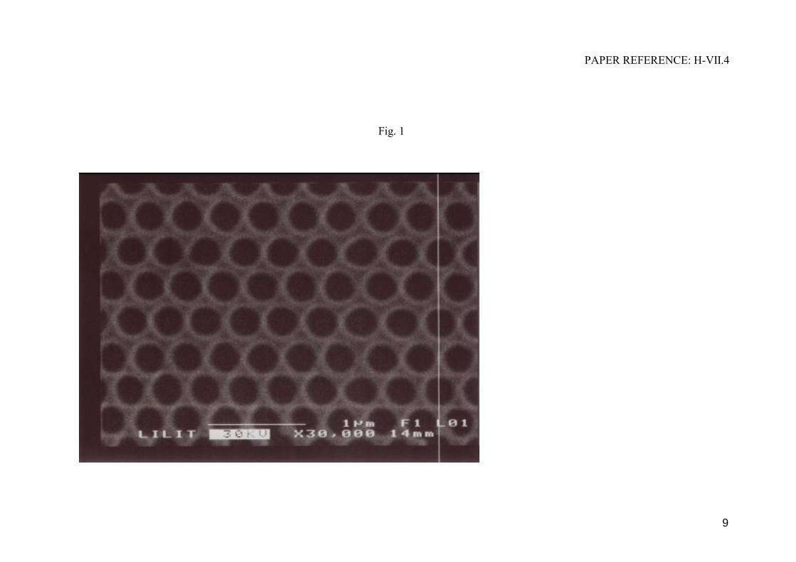
Fig.1 show a SEM micrograph of one of the 2D-structures (array of submicrometric holes with
triangular symmetry) realized by direct-write electron beam lithography on a PMMA coating
spinned onto an a-Si:H film. It is worth to underline that important parameters for the optical
properties of a 2D-photonic crystal are the refractive index of the dielectric slab, the lattice constant
a (inter-hole spacing) and the radius r of the drilled holes. The structure here shown consists of
holes with a radius, r = 0.41a, where a=350 nm realized on a matrix of a-Si:H (with a refractive
index of 3.5 in the low absorption region). Such a structure gives a band gap from 800 nm up to 1.4
μm for TE modes (electric field in the plane of the slab) and two narrow band gaps, from 900nm up
to 950nm and from 1.32 µm to 1.52 µm, for TM modes (electric field perpendicular to the slab), as
verified by a freeware software aimed at computing the dispersion relations of periodic dielectric
structures [7].
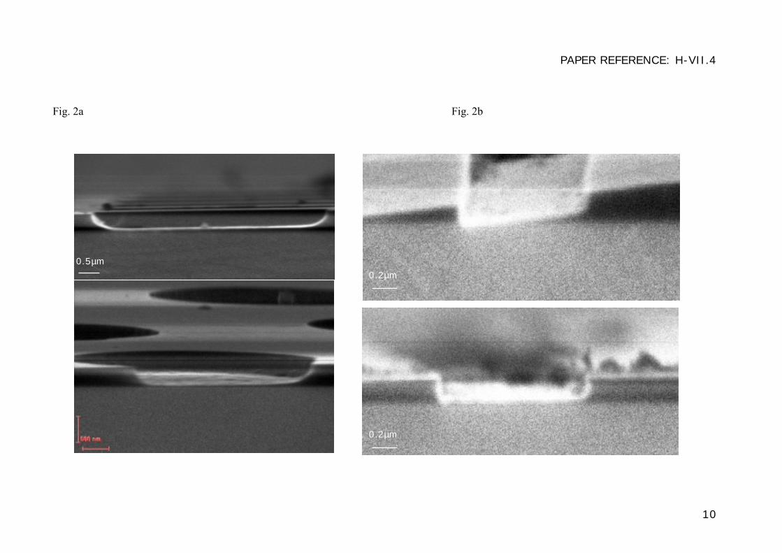
A prerequisite for dimensional control in etching small features is the maintenance of a good
anisotropy and the maximization of etch selectivity and uniformity. The experimental data
concerning with the etching of a-Si:H films performed by the RIE system, have been compared with
that obtained by the ICP. Etch rate and selectivity have been examined as a function of type of gas,
flow rate, pressure and r.f. power.
Focusing on the standard reactive ion etching system (RIE), the process optimisations led to the
results summarized in Table 1. Under the same process conditions, the etch rate of a SF6 plasma is
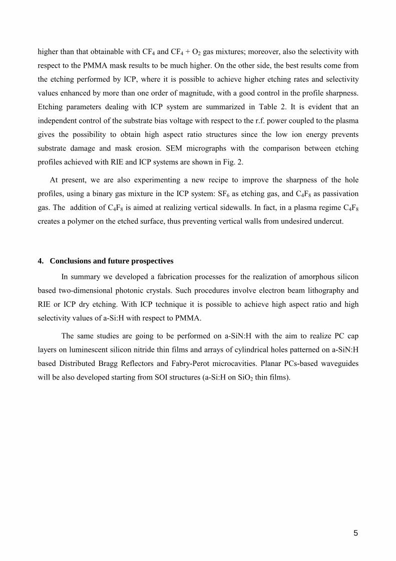
5
higher than that obtainable with CF4 and CF4 + O2 gas mixtures; moreover, also the selectivity with
respect to the PMMA mask results to be much higher. On the other side, the best results come from
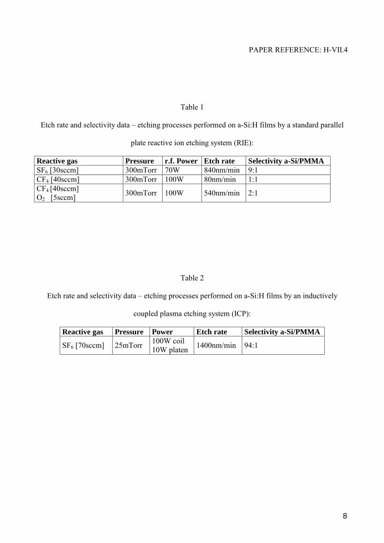
the etching performed by ICP, where it is possible to achieve higher etching rates and selectivity
values enhanced by more than one order of magnitude, with a good control in the profile sharpness.
Etching parameters dealing with ICP system are summarized in Table 2. It is evident that an
independent control of the substrate bias voltage with respect to the r.f. power coupled to the plasma
gives the possibility to obtain high aspect ratio structures since the low ion energy prevents
substrate damage and mask erosion. SEM micrographs with the comparison between etching
profiles achieved with RIE and ICP systems are shown in Fig. 2.
At present, we are also experimenting a new recipe to improve the sharpness of the hole
profiles, using a binary gas mixture in the ICP system: SF6 as etching gas, and C4F8 as passivation
gas. The addition of C4F8 is aimed at realizing vertical sidewalls. In fact, in a plasma regime C4F8
creates a polymer on the etched surface, thus preventing vertical walls from undesired undercut.
4. Conclusions and future prospectives
In summary we developed a fabrication processes for the realization of amorphous silicon
based two-dimensional photonic crystals. Such procedures involve electron beam lithography and
RIE or ICP dry etching. With ICP technique it is possible to achieve high aspect ratio and high
selectivity values of a-Si:H with respect to PMMA.
The same studies are going to be performed on a-SiN:H with the aim to realize PC cap
layers on luminescent silicon nitride thin films and arrays of cylindrical holes patterned on a-SiN:H
based Distributed Bragg Reflectors and Fabry-Perot microcavities. Planar PCs-based waveguides
will be also developed starting from SOI structures (a-Si:H on SiO2 thin films).
6
Acknowledgments
This work has been supported by MURST through the PRIN 2002-2003 project
“Plasmachemical technologies in the deposition of Silicon-based nanostructured films for
photonic and photovoltaic applications“ and by INFM through the project PHOBOS “Photonic
Band gap Materials for Si-based Optoelectronic Structures”
References
[1] J. D. Joannopoulos, R. D. Meade, J. N. Winn, "Photonic Crystals", Ed. Princeton University
Press 1995.
[2] M. Loncar, T. Doll, J. Vuckovic, A. Sherrer, J. Lighwave Techn., Vol. 18, No 10, October 2000.
[3] A. A. Erchak, Daniel J. Ripin, S. Fan, P. Rakich, J. D. Joannopoulos, E. P. Ippen, G. S. Petrich,
L. A. Kolodziejski, Appl. Phys. Lett. 78 (2001) 563.
[4] S. Fan, P. R. Villeneuve, J. D. Joannopoulos, Phys. Rev. Lett. 78 (1997) 3294.
[5] V. Ballarini, G. Barucca, E. Bennici, C.F. Pirri, C. Ricciardi, E. Tresso, F. Giorgis, published in
the same volume.
[6] J.R. Sheats, B.W. Smith, “Microlithography – Science and Technology”, Ed. Marcel Dekker.
[7] MIT Photonic-Bands (MPB) http://ab-initio.mit.edu/mpb/
7
PAPER REFERENCE: H-VII.4
Figure Captions
Fig.1
SEM micrograph of a 2D-structure fabricated by electron beam lithography on a PMMA coating
spinned onto an a-Si:H film. The structure consists of cylindrical holes with a radius, r=0.41a,
where a=350nm is the inter-hole spacing.
Fig.2
Cross-sectional SEM viewgraphs of a-Si:H etched structures: comparison between etching profiles
obtained by RIE (a) and ICP (b) systems.
8
PAPER REFERENCE: H-VII.4
Table 1
Etch rate and selectivity data – etching processes performed on a-Si:H films by a standard parallel
plate reactive ion etching system (RIE):
Reactive gas Pressure r.f. Power Etch rate Selectivity a-Si/PMMA SF6 [30sccm] 300mTorr 70W 840nm/min 9:1 CF4 [40sccm] 300mTorr 100W 80nm/min 1:1 CF4 [40sccm] O2 [5sccm] 300mTorr 100W 540nm/min 2:1
Table 2
Etch rate and selectivity data – etching processes performed on a-Si:H films by an inductively
coupled plasma etching system (ICP):
Reactive gas Pressure Power Etch rate Selectivity a-Si/PMMA
SF6 [70sccm] 25mTorr 100W coil 10W platen 1400nm/min 94:1
9
PAPER REFERENCE: H-VII.4
Fig. 1
10
PAPER REFERENCE: H-VII.4
Fig. 2a Fig. 2b
0.5µm
0.2µm
0.2µm


