Embed Size (px)
Citation preview

c© 2015 Aaron Daniel Ho

ASYMMETRIC INTERLEAVING IN LOW-VOLTAGE CMOS POWERMANAGEMENT WITH MULTIPLE SUPPLY RAILS
BY
AARON DANIEL HO
THESIS
Submitted in partial fulfillment of the requirementsfor the degree of Master of Science in Electrical and Computer Engineering
in the Graduate College of theUniversity of Illinois at Urbana-Champaign, 2015
Urbana, Illinois
Adviser:
Assistant Professor Robert C. N. Pilawa-Podgurski

ABSTRACT
Recent years have seen the proliferation of electronic devices that require
multi-phase power converters to provide heterogeneous power rails to differ-
ent systems. Typical systems will utilize symmetric interleaving as a method
of reducing the input current ripple for the power converter. Asymmetric
interleaving is a method of control that allows for a further reduction, and
in some cases complete cancellation, of this input current ripple. This work
looks at some of the challenges for a practical implementation using digital
control, and provides results to quantify this improvement. This work demon-
strates a control algorithm implementation capable of achieving nearly 3x re-
duction in the input current ripple via the asymmetric interleaving method.
ii

ACKNOWLEDGMENTS
I must express my utmost appreciation towards my thesis adviser Professor
Robert Pilawa-Podgurski. I am grateful for this opportunity and time to
have studied in power electronics under his tutelage and guidance. With
many changes in the direction my education has taken me, he has shown
enormous patience towards me and for that I am forever indebted to him.
To my fellow members of the Pilawa Group and other colleagues of the
Power and Energy Systems Group, thank you for this chance to work along-
side you. Being witness to the incredible minds that this group has gath-
ered has been awe inspiring, and the friendship and encouragement you have
shown me has brought me joy over my time in Illinois. I eagerly await to
hear of the journeys the future has in store for you.
Special thanks go to Professor Steven Franke, the administrative staff of
the ECE department, and the group secretaries Joyce Mast and Robin Smith.
They have been an invaluable resource for navigating life as a graduate stu-
dent.
Thanks go to my family for their unerring love and support in this time.
Thanks go to friends both near and abroad, for the memories this chapter of
life has brought.
iii

TABLE OF CONTENTS
LIST OF ABBREVIATIONS . . . . . . . . . . . . . . . . . . . . . . . v
CHAPTER 1 INTRODUCTION . . . . . . . . . . . . . . . . . . . . 11.1 Introduction . . . . . . . . . . . . . . . . . . . . . . . . . . . . 11.2 Multiphase Switching Converters . . . . . . . . . . . . . . . . 11.3 Principle of Asymmetric Interleaving . . . . . . . . . . . . . . 21.4 Thesis Organization . . . . . . . . . . . . . . . . . . . . . . . . 2
CHAPTER 2 CURRENT RIPPLE REDUCTION VIA ASYM-METRIC INTERLEAVING . . . . . . . . . . . . . . . . . . . . . . 42.1 Concept Description . . . . . . . . . . . . . . . . . . . . . . . 42.2 Shortcomings of Symmetric Interleaving . . . . . . . . . . . . 62.3 Mathematical Derivations . . . . . . . . . . . . . . . . . . . . 92.4 Buck Converter Application Example . . . . . . . . . . . . . . 16
CHAPTER 3 HARDWARE IMPLEMENTATION ALGORITHM . . 213.1 Implementation Details and Control Technique . . . . . . . . . 21
CHAPTER 4 VERIFICATION OF IMPLEMENTATION TECH-NIQUE . . . . . . . . . . . . . . . . . . . . . . . . . . . . . . . . . 244.1 Simulation Verification . . . . . . . . . . . . . . . . . . . . . . 244.2 Experimental Results . . . . . . . . . . . . . . . . . . . . . . . 27
CHAPTER 5 CONCLUSION . . . . . . . . . . . . . . . . . . . . . . 32
APPENDIX A HARDWARE IMPLEMENTATION DETAILS . . . . 33A.1 Schematic Drawings . . . . . . . . . . . . . . . . . . . . . . . 33A.2 PCB Layout . . . . . . . . . . . . . . . . . . . . . . . . . . . . 35
APPENDIX B MATLAB CODE . . . . . . . . . . . . . . . . . . . . 42B.1 Phase dig.m . . . . . . . . . . . . . . . . . . . . . . . . . . . . 42B.2 LUT.m . . . . . . . . . . . . . . . . . . . . . . . . . . . . . . . 55
APPENDIX C MICROCONTROLLER C CODE . . . . . . . . . . . 61
REFERENCES . . . . . . . . . . . . . . . . . . . . . . . . . . . . . . . 77
iv

LIST OF ABBREVIATIONS
CCM Continuous Conduction Mode
CMOS Complementary Metal-Oxide-Semiconductor
CPU Central Processing Unit
DC Direct Current
DPA Distributed Power Architecture
EMI Electromagnetic Interference
FFT Fast Fourier Transform
LUT Look-Up Table
PSC Power Stage Converter
PWM Pulse Width Modulation
SIMO Single Input Multiple Output
VSC Voltage Source Converter
v

CHAPTER 1
INTRODUCTION
1.1 Introduction
Power management plays a critical role in a variety of electrical systems
that are ubiquitous in modern society. This role extends to all economies
of scale, from the national power grid to individual end users of electronic
devices. Therefore, this field of research is crucial for national labs, private
enterprises, and universities.
Recent trends in technology have allowed for the proliferation and wide-
spread use of portable electronics like laptop computers, tablets, and smart
phones. Because portable devices are powered by rechargeable batteries,
these devices require very efficient power management control.
This thesis research is directed to the study of a control method for bat-
tery power management by implementing asymmetric interleaving. Basic
concepts related to this research are introduced in the following sections of
Chapter 1. Thorough elaboration on the theory, implementation, and verifi-
cation will be presented in Chapters 2 through 5.
1.2 Multiphase Switching Converters
Power systems that implement multiphase switching converters can benefit
from reduced voltage and current ripple through the use of interleaving [1,
2, 3, 4, 5], which enables ripple cancellation, where the overall waveform has
reduced ripple characteristics. Consequently, filter components implementing
interleaving techniques (often the largest elements in a power converter) can
be reduced compared to filter components in non-interleaved designs.
For conventional systems with symmetric operating conditions, the tech-
1

nique of ripple cancellation is easily implemented by phase shifting the con-
verters such that adjacent phases are offset by 360/N , where N is the total
number of phases [6, 7, 8]. For systems with asymmetric operation, adjacent
phases are instead offset by varying degrees, complicating calculations and
implementation.
1.3 Principle of Asymmetric Interleaving
The foundation of interleaving is built upon the reduction of voltage or cur-
rent harmonics [9]. This interleaving is analyzed in DC-DC applications
[1, 10], as well as voltage source converter (VSC) systems in the time domain
[11, 12]. It is easy to see a ripple current cancellation effect of interleaving in
time domain, but the analysis in time domain is more difficult. For example,
it is very difficult to study the impact of interleaving on the circulating cur-
rent and the relationship between the harmonic currents reduction, especially
if more than two VSCs are involved in the paralleling system.
Recently, people started to study the impact of interleaving on a paralleled
three-phase VSC system in frequency domain [13, 14, 15, 16]. Using the
double integral Fourier analysis method [17], the output ac harmonic currents
cancellation effect of interleaving for a system of N parallel three-phase VSCs
has theoretically been confirmed [13]. The impact of the non-conventional
interleaving is also discussed in [15, 18, 19] and used in [16]. In summary,
the previous work discussed above mainly focuses on symmetric interleaving
and the impact of interleaving on system harmonic voltages and currents.
1.4 Thesis Organization
This thesis is organized as follows. Chapter 2 provides background informa-
tion on the interleaving technique, comparing a few different implementations
of the technique. Chapter 3 proposes a technique for implementing asym-
metric interleaving in experimental hardware. Chapter 4 provides verification
for the proposed control technique and simulation results that illustrate the
concept and highlight different concerns to be considered. Also included
are measured results from a prototype converter that support the proposed
2

operation. Chapter 5 concludes the thesis.
3

CHAPTER 2
CURRENT RIPPLE REDUCTION VIAASYMMETRIC INTERLEAVING
2.1 Concept Description
In power electronics, multiphase DC-DC converters are widely used because
they enable the processing of high power by splitting the load-current into
multiple phases [20]. Conventional multiphase circuits are supplied by a
common source, and the goal is to distribute the processed power evenly
between the phases. An example circuit is shown in Fig. 2.1 with a single
input, single output, and three phases for power conversion.
Multiphase converters will conventionally implement symmetric interleav-
ing in their control. This will have the added benefit of reducing the current
ripple observed at the aggregate input or output. In the example of the buck
converter topology displayed in Fig. 2.1, Fig. 2.2 shows the ripple waveform
observed in the three inductors. All converters are operated at the same
duty ratio of D = 0.7 and the phase currents are evenly shifted by 120 to
each other. The displayed waveform isum(t) is the sum of all three induc-
tor waveforms neglecting filter effects. It can be seen that its magnitude is
significantly lower than the ripple magnitude in each phase. This yields a
significant reduction of the overall output current ripple. It should be noted
that in this case, isum(t) is the summation of the inductor current at the
output node, so the DC component of the current can be ignored. More
generally, the DC component cannot be summarily ignored and must be
considered when observing the aggregate waveform.
The magnitude of the ripple in the time-domain is significantly reduced
due to effective cancellation of certain ripple harmonics in the frequency-
domain. The fundamental frequency of the ripple is determined by the
switching frequency fsw of the converter. The number of phases N corre-
sponds to the cancellation of the harmonics; e.g. in a symmetrical two phase
4

L1
L2
L3
CIN1
CIN2
CIN3
COUT1
COUT2
COUT3
i1(t)
i2(t)
i3(t)
+−
iin,1(t)
iin,2(t)
iin,3(t)
Vin
LoadVout
iout(t)iin(t)
Figure 2.1: Multiphase dc-dc buck converter with three phases.
0 0.5 1 1.5 2 2.5 3 3.5 4
x 10−5
−3
−2
−1
0
1
2
3
Time / s
i(t)/A
i1
i2(t)i3(t)isum(t)
Figure 2.2: Ripple component of the current in each phase and summedripple components for a three-phase buck-converter operating at D = 0.7.
5

0 1 2 3 4 5 6 7 8 9 10 11 12 13 14 150
0.05
0.1
0.15
0.2
0.25
k
Asum
Figure 2.3: Harmonic content of the summed ripple components for athree-phase buck-converter operating at D = 0.7.
converter all odd harmonics (k = 1, 3, 5, ...) are canceled. Equivalently, for
a symmetrical three-phase converter, harmonics that are multiples of three
(i.e. k = 3, 6, 9, ...) will remain, while the fundamental, second, and other
higher harmonics (k = 1, 2, 4, 5, 7, 8, ...) are canceled. This is illustrated in
Fig. 2.3 which displays an exemplary frequency content of the summed ripple
components in a three-phase interleaved converter at symmetrical operating
conditions.
2.2 Shortcomings of Symmetric Interleaving
Asymmetric phase-shifting has been used to account for imbalances in the
converter phases due to component tolerances [21]. This was done for stan-
dard single-input single-output converter topologies such as shown in Fig. 2.1.
It has been shown in the literature that while conventional symmetric inter-
leaving can still reduce the current ripple in asymmetric systems, a larger
6

reduction can be achieved via a technique called asymmetric interleaving.
Previously, the concept of asymmetric interleaving has been explored in the
context of EMI noise shaping, where certain higher order harmonics can
be reduced, thereby reducing the filter size as dictated by EMI regulations
[22, 23, 24]. Similarly, asymmetric interleaving has been proposed to reduce
sideband harmonics in cascaded H-bridges [25, 26], but as shown in [27, 28],
the methods used to date have suffered from relatively minor improvements
due to the difficulty of sensing aggregate currents, and the delay associated
with the measurements. Moreover, existing methods have primarily been
concerned with component tolerances and their impact of the multi-phase
operation, which is typically relatively minor.
Recent work has investigated the use of asymmetric interleaving in systems
that operate under asymmetric operating conditions by design, such as sub-
module maximum power point tracking in solar photovoltaics [29, 30, 31,
32]. In the case of solar photovoltaics, a variance in radiance conditions
and module characteristics results in each sub-module operating at different
conditions in order to achieve maximum power point tracking [33, 34, 35, 36].
Another situation involves digital systems requiring separate supply rails
for different circuit blocks, such as distributed power architectures (DPA)
and low voltage CMOS power management systems [31, 37]. Portable appli-
cations in particular have driven the development of systems requiring dif-
ferent voltage domains for various sub-systems to finely tune the operating
voltage to minimize power consumption of each individual circuit block [38].
In these applications, it is important to minimize the ripple at the input of
the power management system, as the input ripple current determines both
the required filtering capacitance (comprising a substantial portion of sys-
tem size and weight) and the power loss due to the parasitic resistance of the
battery from any ripple current that is not filtered by the input capacitance.
The contribution of this thesis is the analysis and design of practical asym-
metric interleaving control schemes for a multi-phase converter providing sep-
arate supply voltages, which is often encountered in portable and/or battery-
operated electronics (e.g. smart phones, tablets, laptops, sensors) [39]. The
schematic representation of the system analyzed can be referred to as a sin-
gle input, multiple output, or SIMO, buck converter. A generic example of
a SIMO converter can be seen in Fig. 2.4, where a single dc-bus can be pro-
cessed to different output loads. Even with separate supply voltage rails, it is
7
L1
L2
L3
CIN1
CIN2
CIN3
COUT1
COUT2
COUT3
i1(t)
i2(t)
i3(t)
+−
iin,1(t)
iin,2(t)
iin,3(t)
Load 1
Load 2
Load 3
Vin
iin(t)
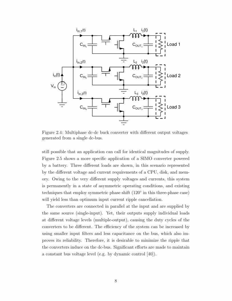
Figure 2.4: Multiphase dc-dc buck converter with different output voltagesgenerated from a single dc-bus.
still possible that an application can call for identical magnitudes of supply.
Figure 2.5 shows a more specific application of a SIMO converter powered
by a battery. Three different loads are shown, in this scenario represented
by the different voltage and current requirements of a CPU, disk, and mem-
ory. Owing to the very different supply voltages and currents, this system
is permanently in a state of asymmetric operating conditions, and existing
techniques that employ symmetric phase shift (120 in this three-phase case)
will yield less than optimum input current ripple cancellation.
The converters are connected in parallel at the input and are supplied by
the same source (single-input). Yet, their outputs supply individual loads
at different voltage levels (multiple-output), causing the duty cycles of the
converters to be different. The efficiency of the system can be increased by
using smaller input filters and less capacitance on the bus, which also im-
proves its reliability. Therefore, it is desirable to minimize the ripple that
the converters induce on the dc-bus. Significant efforts are made to maintain
a constant bus voltage level (e.g. by dynamic control [40]).
8

L1
COUT,1
L2
L3
COUT,2
COUT,3
i IN(t)
VIN
iIN,1(t) i L,1(t)
iIN,2(t)
iIN,3(t) i L,3(t)
i L,2(t)
CIN,1
ICPU
Imemory
Idisk
Figure 2.5: Multiphase dc-dc buck converter from a battery, with digitalloads demanding different voltages and currents.
2.3 Mathematical Derivations
The mathematical derivation of the exact angles required to implement asym-
metric phase shifting is presented in [20, 41]. For the purpose of clarity, as it
is closely related to the work this thesis presents, a summary of the deriva-
tion for a general three-phase system is presented below. As stated in [20],
the two-phase system is trivial in that a 180 phase shift will achieve optimal
but not total cancellation of the fundamental ripple, while a general system
with N phases can be related back to the case of N = 3.
The derivation can be applied to a variety of converter types, as the ma-
jority of topologies feature waveforms similar to the basic buck and boost
converters. For the purpose of this thesis, only the buck converter is pre-
9

CCM
0 DnT T T+DnT0
Iin,n
Imax
t
iin,n(t)
DCM
0 DnT T T+DnT0
Iin,n
Imax
t
iin,n(t)
Figure 2.6: Input current waveforms for a buck converter in CCM (top) andDCM (bottom).
sented, as the application is based upon the buck topology. As a reminder
of the waveforms featured in the buck topology, Fig. 2.6 shows the input
current for a converter in continuous conduction mode (CCM) and discon-
tinuous conduction mode (DCM) while Fig. 2.7 shows the corresponding
output currents.
The differing power and voltage requirements of each phase will result
in asymmetric operating conditions, with different phase currents In, duty
ratios Dn and current ripple ∆In. The overall current ripple ∆isum is found
by summing up the N different ripple components. The ultimate goal is to
optimally reduce the observed current ripple by controlling the phase-shift in
each individual phase. Owing to the nature of the periodic signals, this can
be obtained by focusing on minimizing the fundamental harmonic component
of the ripple. The higher harmonics can be further reduced by the input and
output filters.
To describe the current waveforms, in(t) shown in Figures 2.6-2.7 depen-
dent on the phase-shift angles φ0n, they are represented by the their Fourier
series as
10

CCM
0 DnT T T+DnT0
Iout,n −∆in
Iout,n
Iout,n +∆in
t
iout,n(t)
DCM
0 DnT T T+DnT0
Iout,n
Imax
t
iout,n(t)
Figure 2.7: Output current waveforms for a buck converter in CCM (top)and DCM (bottom).
in(t) =a0
2+∞∑k=1
ak · cos(k(ωt− φ0)) + bk · sin(k(ωt− φ0)) (2.1)
or in terms of the sum of phase-shifted cosine terms as
in(t) =a0
2+∞∑k=1
Ak · cos(k(ωt− φ0)− ψk), (2.2)
where Ak is the magnitude and ψk is the phase of the Fourier coefficient. The
two forms are related by
Ak =√a2k + b2
k (2.3)
and
ψk = atan2(bk, ak), (2.4)
where atan2 is the inverse tangent function, that returns the corresponding
angle in the interval of four quadrants [−π, π]. In the further course of the
derivation, a notation with the pattern Ank is used, where n is the phase
index and k denotes the harmonic order.
The goal of the following derivations is to minimize the variation in current
11

which corresponds to the expression inside the sum of the Fourier series given
in Eq. (2.1) and Eq. (2.2).
The aggregate current can be denoted by isum(t) and is found as a sum-
mation of the phase currents
isum(t) =N∑n=1
in(t). (2.5)
The DC component of the each in(t), ao2
, cannot be affected by any phase
shifting, so we can ignore these terms in subsequent equations. Similarly,
as the goal is to minimize a particular harmonic, the summation term can
be dropped for subsequent equations. While most implementations of the
solution will use k = 1, the equations provide the solution for a generic
harmonic k.
By using Eq. (2.2) and (2.5) and representing the phase-shifted cosine
terms as a sum of phasors with magnitude Ank and phase
θnk = kφ0n + ψnk, (2.6)
the current ripple of a single harmonic can be represented as
ISUM = A1k · e−jθ1k + A2k · e−jθ2k + A3k · e−jθ3k , (2.7)
where ISUM denotes the phasor of the summed current variation.
Determining the phase-shift angles that yield a minimal value of the cur-
rent ripple corresponds to reducing the magnitude of ISUM, yielding
minθ2k,θ3k
∣∣A1k + A2k · e−jθ2k + A3k · e−jθ3k∣∣ , (2.8)
with θ1k = 0 for the simplicity of the expression.
Assuming that a complete cancellation of a particular harmonic compo-
nent k is possible, ISUM = 0 provides a modified Eq. (2.7). By converting
this modified Eq. (2.7) into the Cartesian form and minimizing the real and
imaginary part of the summed phasor, the solution for Eq. (2.8) is found to
be
12

θ2k = cos−1
(1
2· A
23k − A2
2k − A21k
A1k · A2k
)(2.9a)
θ3k = 2π − cos−1
(1
2· A
22k − A2
1k − A23k
A1k · A3k
). (2.9b)
Using this result, the desired phase-shift angles φ01, φ02, and φ03 can be
found using Eq. (2.6). By shifting all the phasors by the value of φ01, the
relative phase shift is still identical while leading to an easier implementation
with φ01 = 0. This yields
φ01 = 0 (2.10a)
φ02 =1
k·[cos−1
(1
2· A
23k − A2
2k − A21k
A1k · A2k
)− ψ2k + ψ1k
](2.10b)
φ03 =1
k·[2π − cos−1
(1
2· A
22k − A2
1k − A23k
A1k · A3k
)− ψ3k + ψ1k
]. (2.10c)
Equations (2.10b) and (2.10c) imply that the arguments of the cos−1 terms
must have an absolute value ∈ [0, 1] in order for the complete cancellation
of the phasor to exist. If this condition for complete cancellation cannot be
met, φ02 and φ03 are set to either 0 or 180, depending on which An1 vector
is determined to be the largest in magnitude. This will minimize the real
component of the summed phasor as much as possible while zeroing out the
imaginary part.
The phasor diagram representing this choice of reference angle can be seen
in Fig. 2.8, for the asymmetric operation conditions as shown in the inset.
It should be noted that symmetric interleaving operates by implementing
a symmetric phase shift of φ02 = 120 and φ03 = 240. In the symmetric case,
the Fourier coefficients (ank and bnk) are identical for the different phases.
Consequently, the ψnk values (as calculated in (2.4)) are also identical, and
the corresponding phasor angles θnk have the same relative phase shift as
the implemented phase-shift angles φ0n. Therefore, for symmetric operating
conditions, a phase shift of φ02 = 120 and φ03 = 240 is functionally identical
to θ21 = 120 and θ31 = 240.
However, in the case of asymmetric operating conditions between phases,
each phase can yield a unique ψnk and Ank. The result, as implied by Eq. 2.6,
13

Real Part
Imaginary
Part
−0.6
−0.4
−0.2
0
0.2
0.4
0.6
−0.6 −0.4 −0.2 0 0.2 0.4 0.6
Iout,1= 0.8A, D1 = 0.55, φ01 = 0, θ11 = 0
Iout,2= 1.0A, D2 = 0.65, φ02 = 132, θ21 = 150
Iout,3= 0.6A, D3 = 0.75, φ03 = 224, θ31 = 270
Isum
Figure 2.8: Asymmetric phasor diagram for fundamental component withoptimum asymmetric phase shift.
is that a control implementing φ02 = 120 and φ03 = 240 does not necessarily
result in θ21 = 120 and θ31 = 240. This can clearly be seen by compar-
ing Fig. 2.9 and Fig. 2.10, which shows the phasor diagram for the same
operating conditions as that of Fig. 2.8, but with φ0n and θn1 with uniform
120 separation, respectively. In practice, it is the time-domain phase shift
shown in Fig. 2.9 that is commonly used when symmetric interleaving (120
separation for a three-phase system) is used under asymmetric operating con-
ditions. It can be seen that in both cases, the fundamental component is not
cancelled, owing to the asymmetry of the different phasors. Thus, while the
distinction between φ0n and θn1 is needed for the purpose of explaining the
seeming asymmetry in Fig. 2.9, it does not alter the premise of deriving a
complete or reduced ripple cancellation.
14

Real Part
Imaginary
Part
−0.6
−0.4
−0.2
0
0.2
0.4
0.6
−0.6 −0.4 −0.2 0 0.2 0.4 0.6
Iout,1= 0.8A, D1 = 0.55, φ01 = 0, θ11 = 0
Iout,2= 1.0A, D2 = 0.65, φ02 = 120, θ21 = 138
Iout,3= 0.6A, D3 = 0.75, φ03 = 240, θ31 = 287
Isum
Figure 2.9: Asymmetric phasor diagram for fundamental component withsymmetric phase shift in the time domain. Notice the remaining ripplecomponent at the fundamental.
−0.6
−0.4
−0.2
0
0.2
0.4
0.6
−0.6 −0.4 −0.2 0 0.2 0.4 0.6
Real Part
Imaginary
Part
Iout,1= 0.8A, D1 = 0.55, θ11 = 0
Iout,2= 1.0A, D2 = 0.65, θ21 = 120
Iout,3= 0.6A, D3 = 0.75, θ31 = 240
Isum
Figure 2.10: Asymmetric phasor diagram with symmetric phase shift in thephasor reference frame. Notice the remaining ripple component due to thediffering magnitude of the fundamental phasors of the three phases.
15

2.4 Buck Converter Application Example
In order for equations presented in Section 2.3 to be utilized, it is necessary
to calculate the phasor magnitude Ank and phase ψnk from the Fourier series
of the relevant current waveforms. To illustrate input ripple cancellation in
CCM, a DC-DC buck converter is selected here. While the individual details
for deriving the values for Ank and ψnk differ between topology and operating
point, the general procedure will be identical.
2.4.1 Input Ripple Cancellation
For a buck converter topology, as seen in Fig. 2.5, or other buck-type topolo-
gies, the continuous conduction mode (CCM) input current waveform is
shown in Fig. 2.6. The input current waveform can also be defined in terms
of the inductor current, as seen in Fig. 2.11. This allows for the time domain
representation of this waveform to be expressed as:
iin(t) =
∆IDTt+ Iout − ∆I
2, for kT ≤ t ≤ kT +DT
0, for kT +DT ≤ t ≤ (k + 1)T
k = 0, 1, 2...
(2.11)
where Iout refers to the average output current, D to the duty cycle, and ∆I
the current ripple observed in the inductor.
From Eq. (2.11), the coefficients a and b are computed as
an0 = 2 · Iout,n ·Dn (2.12a)
ank =
(∆In2kπ
+Iout,nkπ
)sin (2kπDn) + (2.12b)
∆In2k2π2Dn
(cos (2kπDn)− 1)
16

time \s
i in(t)\A
0I o
ut−
∆I/2
Iout
I out+
∆I/2
0 DnT T T + DnT 2T
Figure 2.11: Input current waveform for buck-type converter in CCMoperation.
bnk =
(∆In2kπ− Iout,n
kπ
)(cos (2kπDn)− 1) + (2.12c)
∆In2k2π2Dn
sin (2kπDn)
From Eq. (2.3) and (2.4), the phasor representation is found as
Ank =2sin (kπDn)
2k2π2Dn
· sqrt ( (2.13a)
∆I2n
[k2π2D2
n − 2kπDnsin (2kπDn) + 1]
+
4k2π2D2nIout,n [∆Incos (2kπDn) + Iout,n]
)
ψnk = atan2(bnk, ank) =
arctan (arg) ank > 0
arctan (arg) + π bnk ≥ 0, ank < 0
arctan (arg)− π bnk < 0, ank < 0
+π2
bnk > 0, ank = 0
−π2
bnk < 0, ank = 0
not defined bnk = 0, ank = 0
(2.13b)
arg =(2Iout,n −∆In)kπDnsin(kπDn) + ∆Incos(kπDn)
(2Iout,n + ∆In)kπDncos(kπDn)−∆Insin(kπDn)(2.13c)
In the case of buck converter topologies, this current ripple can be ex-
17

pressed in terms of the input voltage, duty cycle, switching frequency, and
inductor values as
∆I =Vin(1−D)D
fswL(2.14)
where Vin, fsw and L are the input voltage, switching frequency, and inductor
value respectively. Of the parameters listed in Eq. (2.12) and (2.14), the two
critical variables are the output current and duty cycle. Every other vari-
able can be considered as a constant. However, because the current ripple
magnitude ∆In is dependent on the inductor value L of the converter, the
proposed technique can also be applied to compensate for component value
tolerances among different phases.
For easier understanding, the cancellation of a harmonic component of the
summed ripple current is illustrated in the time domain and in the frequency
domain here. The harmonic index k is set to one, which yields a matching
of the fundamental components of the Fourier series.
Figures 2.12 and 2.13 show the phasor diagram and time domain represen-
tation of a N = 3 system operating at 1MHz, with duty ratios of D1 = 0.55,
D2 = 0.65, D3 = 0.75, and average output currents of Iout,1 = 0.8A,
Iout,2 = 1.0A, Iout,3 = 0.6A, as an example. Both figures examine the funda-
mental harmonic of the signal and visually demonstrate that the aggregate
can be canceled out simply by shifting phase. In a practical implementation,
this will be the course of action to take, as the operating point dictated by
the application will fix the magnitude of the harmonics.
The values of θ11, θ21 and θ31 have been obtained by performing the out-
lined calculation steps. The parameters and results are displayed in Fig. 2.8.
The angles φ01, φ02 and φ03, by which the fundamental harmonic components
need to be shifted, can now easily be obtained. In most power electronics
implementations it is desirable to reduce the fundamental Fourier component
of the switching ripple waveform, as this is typically the largest component
in practically encountered waveforms (e.g. square and triangle-waves).
18

Figure 2.12: Phasor comparison of a system symmetrically shifting the φ’s(lighter arrows) and a system asymmetrically shifting the φ’s (darkerarrows).
19

Figure 2.13: Time domain comparison of fundamental harmonics, wherethe lighter signal represents a symmetrically shifted system and the darkersignal represents the asymmetrically shifted system.
20

CHAPTER 3
HARDWARE IMPLEMENTATIONALGORITHM
3.1 Implementation Details and Control Technique
In order to adjust the phase shift dynamically, the relative phase shifts must
be calculated for the given operating conditions. Several factors must be con-
sidered such as the computational ability of the controller, execution speed,
and memory limitations. The math required, as derived in [20] and discussed
in Chapter 2, involves a number of trigonometric functions, which are tra-
ditionally viewed as computationally intensive instructions, in particular if
implemented on low-cost hardware. Additionally, the input ripple cancella-
tion equations as discussed in Section 2.4 indicate a greater complexity in
generating the phasor magnitudes in comparison to the output ripple appli-
cation [20].
Instead of directly computing the phase shifts required, it is possible to
utilize a look-up table (LUT).
For a three-phase system as depicted in Fig. 2.5, there are six variables
that must be considered: the three average current values Iout,n and the three
duty cycles Dn.
The fastest implementation would be to use a direct, six-dimensional look-
up table to reduce computation times. The drawback here is resolution and
memory. If each dimension maintained 10 possible values, corresponding
to a coarse resolution of roughly 10%, the table would have a million val-
ues, each requiring two bytes to maintain values between 0 and 360. The
required memory (2000 kB) would thus be out of reach for typical digital
implementations on low-cost microcontrollers.
To address this concern, we propose to break up the look-up method into
two main steps:
1. Determine the fundamental components of the signal phasors given the
21
operational condition, including both magnitude An1 and phase ψn1
2. Use the values of An1 and ψn1 to determine φ02,φ03.
Step 1 is performed by using Eqs. (2.11), (2.12), and (2.13) to calculate
An1 and ψn1. Because the computation of the phasor representation depends
only on the operating conditions of a single phase, a set of look-up tables can
be constructed that take Iout,n and Dn as inputs for any phase and return An1
and ψn1. Because the same LUT can be used for any phase, this reduces the
memory space for this step, and enables a finer resolution to be implemented
for Iout and D. In Step 2, An1 and ψn1 must be used to determine φ0n. It
should be reiterated that from Eqs. (2.9a) and (2.9b), the solutions for θn1
only depend on An1, not ψn1. Further, even if the exact values of An1 are not
immediately known, they can be expressed as ratios, with the largest An1
value in the denominator of each ratio. Rearranging Eqs. (2.10b) and (2.10c)
further yields six modified equations:
θ21 = cos−1
(A31
A11
)2
−(A21
A11
)2
− 1
2A21
A11
(3.1a)
θ31 = 2π − cos−1
(A21
A11
)2
−(A31
A11
)2
− 1
2A31
A11
(3.1b)
when A11 is the max,
θ21 = cos−1
(A31
A21
)2
− 1−(A11
A21
)2
2A11
A21
(3.2a)
θ31 = 2π − cos−1
1−(A31
A21
)2
−(A11
A21
)2
2A11
A21
A31
A21
(3.2b)
when A21 is the max, and
θ21 = cos−1
1−(A21
A31
)2
−(A11
A31
)2
2A11
A31
A21
A31
(3.3a)
22

θ31 = 2π − cos−1
(A21
A31
)2
− 1−(A11
A31
)2
2A11
A31
(3.3b)
when A31 is the max.
Consequently, one value of A11, A21, and A31 will be normalized to 1 and the
other two values are ∈ [0, 1]. Eqs. (3.1), (3.2), and (3.3) are used to construct
another set of look-up tables, where the normalized values Anormalized,n are
inputs, and θ21 and θ31 are outputs. From this, φ02 and φ03 can be obtained
through (2.6) and the knowledge of ψn1, from step 1, and θn1.
None of the tables individually directly yield the desired value of φn1.
Rather, the proposed LUT implementation reintroduces some computational
steps and comparisons. Following step 1, computations are needed to deter-
mine which An1 vector is the largest and subsequently the normalized values
of the other two An1 vectors. However, these are comparably simple calcula-
tions with minimum computational overhead.
With the decision to implement a series of LUTs, there are three resolu-
tions that will affect the system performance: Iout, D, and Anormalized. The
parameters D and Anormalized are naturally ranging from 0 to 1, while the
current Iout can be stored either as a normalized value from 0 to 1, or directly
as a true current value, if so desired.
23

CHAPTER 4
VERIFICATION OF IMPLEMENTATIONTECHNIQUE
4.1 Simulation Verification
To verify the efficacy of the proposed ripple reduction method of [37] and to
validate the proposed control method, simulations in MATLAB and LTSpice
were carried out to closely emulate the hardware resolution limitations of
the prototype converter. The buck topology of Fig. 2.5 was simulated in
two steps. First, MATLAB simulations were conducted to compare the LUT
implementation and a conventional symmetric phase-shifted implementation.
Second, LTSpice simulations were conducted to compare a conventional sym-
metric phase-shift system, an ideally controlled system with directly calcu-
lated phase-shift solutions, and a system that implemented the proposed
LUTs and was further restricted by imposed hardware resolution limits.
Table 4.1 details the operating conditions for the simulation as well as
subsequent hardware testing. For these operational conditions, the ideal
phase angles were determined to be φ01 = 0, φ02 = 132 and φ03 = 224.
The corresponding phasor can be seen in Fig. 2.8, while Fig. 4.1 details the
Fourier components of the total ripple. which clearly illustrate the reduction
in magnitude of the fundamental component.
Table 4.1: Operational Conditions
Vin 2.0VVout,1, Iout,1 1.1 V, 0.8 AVout,2, Iout,2 1.3 V, 1.0 AVout,3, Iout,3 1.5 V, 0.6 Afsw 1 MHzfPWM 64 MHz
The LTSpice simulations also verify the use of the mathematical model
and the practical implementation. Figures 4.2 and 4.3 show the voltage
24

k
Asum
,k
0
0.1
0.3
0.5
1 2 3 4 5 6 7 8 9 10
0.2
0.4
1 2 3 4 5 6 7 8 9 10
Even Phase Shift
Proposed Digital Phase Shift
Figure 4.1: Fourier component magnitudes of the proposed asymmetricphase shift (with resolution limitations) and conventional, symmetric phaseshift.
ripple and current ripple observed at the input node (corresponding to Iin of
Fig. 2.5). Both the current and voltage ripples of the proposed asymmetric
phase shift feature a reduction in ripple when compared to the conventional,
symmetric phase-shifted implementation. The waveforms and fast Fourier
transform (FFT) also demonstrate that the hardware restricted system op-
erates similarly to the ideally controlled system, with the digital resolution
providing minute differences.
This is to be expected, because using a LUT and hardware with a 1.5625%
time \µs
Voltage\V
1.94
1.96
1.98
2
2.02
2.04
430 431 432 433
∆V=89.5 mV
∆V=45 mV
∆V=38.7 mV
Veven Vproposed Vdig ita l
Figure 4.2: Input voltage ripple.
25

time \µs
Current\A
0.5
0.75
1
1.25
1.5
1.75
2
2.25
2.5
2.75
150 151 152 153
∆I=1.97 A
∆I=1.52 A
∆I=1.53 A
Ieven Iproposed Idig ita l
Figure 4.3: Input current ripple.
resolution should not result in a significant change in the waveform. The FFT
of the current, observed in Fig. 4.4, more clearly shows the effects of the pro-
posed LUT implementation. The potential reduction in current ripple at
the fundamental 1 MHz is nearly 30 dB, but the practical implementation is
limited to a smaller, but still significant, reduction of 15 dB.
Frequency \Hz
−100
−75
−50−45.99
−31.88−25
−16.89
0
100e3 1e6 5e6
29.1 dB 14.99 dB
Ieven
Idigital
Iproposed
Figure 4.4: Fast Fourier transform of Fig. 4.3, illustrating the reducedfundamental ripple component resulting from the proposed asymmetricphase shift method.
26

4.2 Experimental Results
A prototype of a hardware implementation has been designed. The operating
conditions are described in Table 4.1, while Table 4.2 details some of the spe-
cific hardware used for this prototype. All the hardware is readily available
from vendors, with the exception of the custom IC used for the power stage.
The custom IC is the regulation buck stage of the two-stage converter devel-
oped in [42], allowing for low voltage buck converter operation. Figure 4.5 is
an annotated photograph of the prototype.
The microcontroller (MC) contains three power stage controllers (PSCs),
allowing for easy control for a three-phase system. Following the calculation
of the uneven phase shift, whether by direct calculations or by LUT imple-
mentation, the internal timer of the MC is used to start and adjust the PSCs,
resulting in the desired phase shift.
Table 4.2: Component Listing
Device Model Value Manufacturer
Integrated Power Stage Custom IC 180 nm CMSrH,on 82.2mΩrL,on 53.9mΩInductor LQM2HP-G0 Series 1 µH MurataInput Capacitor 0402, X5R, 6.3V 4 x 0.1 µF TDKOutput Capacitor 0402, X5R, 6.3V 4 x 10 µF TDKMicrocontroller AT90PWM316 Atmel
4.2.1 Implementation Comparison
The main tradeoffs discussed in Section 3.1 are between computation time,
memory usage, and accuracy. In these results, the LUT sizes were based on
step sizes of 10% for D, 0.2A for Iout (range of 0 to 1.6 A), and 10% for
Anormalized. The MC used is an Atmel AT90PWM316, with 16kB of memory.
Table 4.3 details the comparison between directly calculating the phase
angle and utilizing the proposed LUT method. For the time required to
calculate the phase angles, direct calculations required 2.25 ms, while the
LUT needed 603.7 µs. This is a reduction in calculation time of nearly 73%.
It should be noted, however, that in this particular implementation, the
mechanism used to update the PSC of the microcontroller was the dominant
27

Figure 4.5: Annotated photograph of prototype converter.
Table 4.3: Comparison Between Implementation Schemes
Direct Calculation LUT method
Calculation time 2.25 ms 603.7 µsφ02 130.5 122.9
φ03 223.9 226.6
Memory Needed 3.86kB 7.27kB
delay of the system, taking a full 10 ms. Other microcontrollers or CMOS
implementations would not suffer from this long delay, however.
Also shown in Table 4.3 are the unique phase shift angles φ02 and φ03,
as computed through the direct calculation and the proposed LUT method
(which used a relatively coarse resolution). It can be seen that the LUT
method does result in a small error of the phase angles compared to the ideal
mathematical solution, which in turn will give rise to a less than optimal
ripple reduction, as confirmed through experimental measurements.
The memory required for the MC code when directly calculating the phase
angles was 3.86kB. When implementing the LUT, the memory usage nearly
doubles to 7.27kB. This is already using a fairly coarse LUT. If the resolution
were to be made finer, this memory requirement would increase even further,
making a full LUT method impractical in both microcontroller and direct
CMOS implementations.
28

4.2.2 Ripple Reduction Achieved
Experimental measurements have been performed on the prototype con-
verter, and the effectiveness of the three different approaches (conventional
symmetric phase shift, optimum asymmetric phase shift, and LUT-assisted
phase shift) has been quantified. All measurements presented here were
obtained for the operating conditions Vin = 2 V, duty cycles D1 = 0.55,
D2 = 0.65, and D3 = 0.75, and output currents I1 = 0.8A, I2 = 1.0A, and
I3 = 0.6A.
Symmetric Phase Shift
Asymmetric Phase Shift - Optimal
LUT-Assisted Phase Shift
Figure 4.6: Measured input current ripple for different phase shiftimplementations.
Fig 4.6 compares the input current measured for this system. When apply-
ing a symmetric phase-shift (φ01 = 0, φ02 = 120, and φ03 = 240) the input
current ripple is found to be 32.8 mA for the prototype converter. When the
optimum asymmetric phase shift is employed (φ01 = 0, φ02 = 130.5, and
φ03 = 223.9), the current ripple is reduced to 11.2 mA, an improvement of
65.8%. Using the LUT-assisted method, resulting in φ01 = 0, φ02 = 122.9,
and φ03 = 226.6, the current ripple is found to be 14.8 mA, an improvement
of 54.9% compared to conventional symmetric phase shift.
Similarly, Fig 4.7 compares the input voltage measured for this system,
29

Symmetric Phase Shift
Asymmetric Phase Shift - Optimal
LUT-Assisted Phase Shift
Figure 4.7: Measured input voltage ripple for different phase shiftimplementations.
according to Fig. 2.5. When applying an symmetric phase-shift the voltage
ripple is found to be 280 mV. The optimum asymmetric phase shift yields
a voltage ripple of 108 mV, an improvement of 61.4%. When the converter
employs the LUT assisted method the resulting voltage ripple is found to be
140mV, an improvement of 50% compared to the symmetric case.
An analysis of the frequency content of these ripple waveforms provides
another method to evaluate the proposed technique, as the mathematical
justification is the reduction of the fundamental Fourier component. The
FFT for the different signals was calculated using the mathematical tool set
of the oscilloscope.
Figure 4.8 shows results for input current signals. It can be clearly seen
that the fundamental component of the current ripple is reduced by 15-20
dB compared to the conventional symmetric phase shift method. Our exper-
imental results thus affirm the improvements in ripple reduction achievable
through the proposed asymmetric interleaving technique.
30

Symmetric Phase Shift
Asymmetric Phase Shift - Optimal
LUT-Assisted Phase Shift
Figure 4.8: Frequency spectrum of input current showing reduction offundamental Fourier component for different phase shift methods.
31

CHAPTER 5
CONCLUSION
A practical implementation for the control strategy of an asymmetric multi-
phase system has been described. It can be implemented on real hardware,
with little loss of ripple reduction capability compared to theoretical pre-
dictions. As demonstrated in accordance with simulations and hardware
experimental results, the utilization of a LUT still allows for a reduction of
the current ripple beyond what conventional symmetric phase shifted sys-
tems are capable of. By utilizing a LUT, the control hardware is able to
dynamically adjust the phase shift over time, responding to changes in the
operating conditions and the measured current.
32

APPENDIX A
HARDWARE IMPLEMENTATIONDETAILS
A.1 Schematic Drawings
Figure A.1: Schematic drawing of the microcontroller.
33
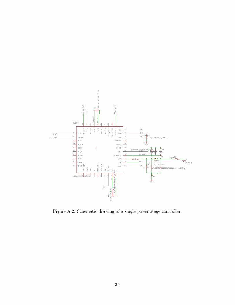
Figure A.2: Schematic drawing of a single power stage controller.
34

A.2 PCB Layout
Figure A.3: Top layer PCB layout.
35

Figure A.4: Bottom layer PCB layout.
36

Figure A.5: Top layer copper.
37

Figure A.6: Middle layer 1 copper.
38

Figure A.7: Middle layer 2 copper.
39

Figure A.8: Bottom layer copper.
40
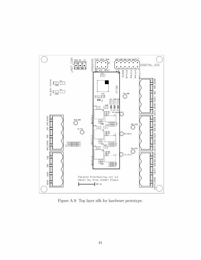
Figure A.9: Top layer silk for hardware prototype.
41

APPENDIX B
MATLAB CODE
B.1 Phase dig.m
The following code contains the analysis of the proposed interleaving tech-
nique. Given certain operating conditions and parameter values, the function
calculates the phase shift necessary to minimize the fundamental ripple and
presents a graphical representation of this phase shift. There are two compar-
isons that are also presented for analysis. First is the efficacy of the proposed
asymmetric interleaving technique compared to a system using the typical
symmetric interleaving as well as a system with no interleaving at all. Second
is comparing an exact solution and a LUT implemented solution.
This version of the code, phase dig, generates the LUT values as integer
values, so as to further approximate the digitization that occurs when imple-
mented in hardware. An earlier version, phase shift, is identical in purpose
but uses exact values in the LUT table generation.
1 function [ph2 ph3 ph2ts ph3ts Am Amns Amts Amr Amnsr
Amtsr] = phase_dig(D1 ,D2 ,D3,I1,I2,I3,Ires ,Dres ,st)
2 %Returns needed phase shift to implement , as well as
the value of the
3 %fundamental ripple after:
4 %-assymetric shift
5 %-no interleaving shift (phi ’s=0)
6 %-typical shift - phi ’s=120 ,240
7 %Hopefully accounts for difference between theta ’s and
phi ’s.
8 %attempting to generate everything to be as small in
terms of digital
9 %values as possible
10 %assumed operating variables - can change for
different precomputation
11 %values
12 Vin =2;
42

13 T=1e-6;
14 L=1e-6;
15 %resolution variables - change for different LUT sizes
16 % st =0.05;
17 % Ires =.1;
18 % Dres =.01;
19 Iavg =0: Ires :1.6;
20 D=0: Dres :1;
21 for j=1: length(D)
22 for k=1: length(Iavg)
23 a(j,k)=Vin*(1-D(j))*D(j)*T/2/pi/L*sin(2*pi*D(j
))+Vin*(1-D(j))*T/2/pi^2/L*(cos(2*pi*D(j))
-1)+Iavg(k)/pi.*sin (2*pi*D(j));
24 b(j,k)=-Vin*(1-D(j))*D(j)*T/2/pi/L*cos(2*pi*D(
j))+Vin*(1-D(j))*T/2/pi^2/L*sin(2*pi*D(j))-
Iavg(k)/pi*(cos (2*pi*D(j)) -1)-Vin*(1-D(j))*
D(j)*T/2/pi/L;
25 A_LUT(j,k)=sqrt(a(j,k).^2+b(j,k).^2);
26 psi_LUT(j,k)=atan2(b(j,k),a(j,k));
27 if(psi_LUT(j,k) <0)
28 psi_LUT(j,k)=psi_LUT(j,k)+2*pi;
29 end
30 end
31 end
32 maxA=max(max(A_LUT));
33
34 A_LUT=floor (255.9.* A_LUT ./maxA);
35 psi_LUT=round(rad2deg(psi_LUT));
36 %Generate LUT from earlier attempt - normalize with
largest fundamental
37 %value of A
38
39 A=st:st:1;
40 %For discrete implementation , probably will be
rounding to a certain size
41 %resolution , dependent on the PWM clock and switching
frequency , where a
42 %full 2*pi radian is covered in PWM/f_sw clicks.
43 PWM =64e6;
44 f_sw=1e6;
45 res=floor(PWM/f_sw);
46
47 %Case 1 - A_1 is max
48 %A(j) corresponds to A_2 , A(k) to A_3
49 for j=1: length(A)
50 for k=1: length(A)
51 theta21(j,k)=round(rad2deg(acos (.5*(A(k)^2-A(j
43
)^2-1) /(1*A(j)))));
52 if(~ isreal(theta21(j,k)))
53 theta21(j,k)=180;
54 end
55 theta31(j,k)=round(rad2deg (2*pi -acos (.5*(A(j)
^2-1-A(k)^2) /(1*A(k)))));
56 if(~ isreal(theta31(j,k)))
57 theta31(j,k)=180;
58 end
59 end
60 end
61
62
63 %Case 2 - A_2 is max
64 %A(j) corresponds to A_1 , A(k) to A_3
65 for j=1: length(A)
66 for k=1: length(A)
67 theta22(j,k)=round(rad2deg(acos (.5*(A(k)^2-A(j
)^2-1) /(1*A(j)))));
68 if(~ isreal(theta22(j,k)))
69 theta22(j,k)=180;
70 end
71 theta32(j,k)=round(rad2deg (2*pi -acos (.5*(1 -A(j
)^2-A(k)^2)/(A(j)*A(k)))));
72 if(~ isreal(theta32(j,k)))
73 theta32(j,k)=360;
74 end
75 end
76 end
77
78 %Case 3 - A_3 is max
79 %A(j) corresponds to A_1 , A(k) to A_2
80 for j=1: length(A)
81 for k=1: length(A)
82 theta23(j,k)=round(rad2deg(acos (.5*(1 -A(j)^2-A
(k)^2)/(A(j)*A(k)))));
83 if(~ isreal(theta23(j,k)))
84 theta23(j,k)=0;
85 end
86 theta33(j,k)=round(rad2deg (2*pi -acos (.5*(A(k)
^2-A(j)^2-1)/(A(j)*1))));
87 if(~ isreal(theta33(j,k)))
88 theta33(j,k)=180;
89 end
90 end
91 end
92 ceil(D1/Dres)
44

93 ceil(I1/Ires)
94 ceil(D2/Dres)
95 ceil(I2/Ires)
96 ceil(D3/Dres)
97 ceil(I3/Ires)
98 A1=A_LUT(ceil(D1/Dres),ceil(I1/Ires))
99 A2=A_LUT(ceil(D2/Dres),ceil(I2/Ires))
100 A3=A_LUT(ceil(D3/Dres),ceil(I3/Ires))
101 psi1=psi_LUT(ceil(D1/Dres),ceil(I1/Ires))
102 psi2=psi_LUT(ceil(D2/Dres),ceil(I2/Ires))
103 psi3=psi_LUT(ceil(D3/Dres),ceil(I3/Ires))
104 size(A_LUT)
105 1/Dres *1.6/ Ires
106 size(theta21)
107 1/st^2
108 if(A1 >=A2 && A1 >=A3) %Case1
109 disp(’Case1’)
110 ind1=floor(A2/A1/st)
111 ind2=floor(A3/A1/st)
112 if(ind1 ==0)
113 ind1 =1;
114 end
115 if(ind2 ==0)
116 ind2 =1;
117 end
118 th2=theta21(ind1 ,ind2)
119 th3=theta31(ind1 ,ind2)
120 elseif(A2 >=A1 && A2 >=A3) %Case2
121 disp(’Case2’)
122 ind1=floor(A1/A2/st)
123 ind2=floor(A3/A2/st)
124 if(ind1 ==0)
125 ind1 =1;
126 end
127 if(ind2 ==0)
128 ind2 =1;
129 end
130 th2=theta22(ind1 ,ind2)
131 th3=theta32(ind1 ,ind2)
132 else %Case3
133 disp(’Case3’)
134 ind1=floor(A1/A3/st)
135 ind2=floor(A2/A3/st)
136 if(ind1 ==0)
137 ind1 =1;
138 end
139 if(ind2 ==0)
45

140 ind2 =1;
141 end
142 th2=theta23(ind1 ,ind2)
143 th3=theta33(ind1 ,ind2)
144 end
145 ph2=round(th2 -round(psi2)+round(psi1))
146 ph3=round(th3 -round(psi3)+round(psi1))
147 ph2ts =120
148 ph3ts =240
149 exp(-1i*(ph2+psi2))
150 exp(-1i*( ph2ts+psi2))
151 Am=abs(A1*exp(-1i*deg2rad(psi1))+A2*exp(-1i*deg2rad(
ph2+psi2))+A3*exp(-1i*deg2rad(ph3+psi3)))
152 Amns=abs(A1*exp(-1i*deg2rad(psi1))+A2*exp(-1i*deg2rad(
psi2))+A3*exp(-1i*deg2rad(psi3)))
153 Amts=abs(A1*exp(-1i*deg2rad(psi1))+A2*exp(-1i*deg2rad(
ph2ts+psi2))+A3*exp(-1i*deg2rad(ph3ts+psi3)))
154 % ph2=rad2deg(ph2)
155 % ph3=rad2deg(ph3)
156 % ph2ts=rad2deg(ph2ts)
157 % ph3ts=rad2deg(ph3ts)
158
159
160
161 samp =50;
162
163 %
164 t=0:T/5000:5*T;
165 s=1: samp;
166 delI1=Vin*(1-D1)*D1*T/L
167 delI2=Vin*(1-D2)*D2*T/L
168 delI3=Vin*(1-D3)*D3*T/L
169 a01=I1*D1%+delI1*D1/2;
170 a02=I2*D2%+delI2*D2/2;
171 a03=I3*D3%+delI3*D3/2;
172 sig1_1 (1: length(t))=a01;sig1_2 (1: length(t))=a01;sig1_3
(1: length(t))=a01;
173 sig2_1 (1: length(t))=a02;sig2_2 (1: length(t))=a02;sig2_3
(1: length(t))=a02;
174 sig3_1 (1: length(t))=a03;sig3_2 (1: length(t))=a03;sig3_3
(1: length(t))=a03;
175 a1=Vin*(1-D1)*D1*T/2./s/pi/L.*sin (2*pi*s*D1)+Vin*(1-D1
)*T/2/pi^2./s.^2/L.*(cos(2*pi*s*D1) -1)+I1./s/pi.*
sin(2*pi*s*D1);
176 b1=-Vin*(1-D1)*D1*T/2./s/pi/L.*cos (2*pi*s*D1)+Vin*(1-
D1)*T/2/pi^2./s.^2/L.*sin (2*pi*s*D1)-I1./s/pi.*( cos
(2*pi*s*D1) -1)-Vin*(1-D1)*D1*T/2/pi/L./s;
46

177 A1s=sqrt(a1.^2+b1.^2);
178 psi1s=atan2(b1,a1);
179 a2=Vin*(1-D2)*D2*T/2./s/pi/L.*sin (2*pi*s*D2)+Vin*(1-D2
)*T/2/pi^2./s.^2/L.*(cos(2*pi*s*D2) -1)+I2./s/pi.*
sin(2*pi*s*D2);
180 b2=-Vin*(1-D2)*D2*T/2./s/pi/L.*cos (2*pi*s*D2)+Vin*(1-
D2)*T/2/pi^2./s.^2/L.*sin (2*pi*s*D2)-I2./s/pi.*( cos
(2*pi*s*D2) -1)-Vin*(1-D2)*D2*T/2/pi/L./s;
181 A2s=sqrt(a2.^2+b2.^2);
182 psi2s=atan2(b2,a2);
183 a3=Vin*(1-D3)*D3*T/2./s/pi/L.*sin (2*pi*s*D3)+Vin*(1-D3
)*T/2/pi^2./s.^2/L.*(cos(2*pi*s*D3) -1)+I3./s/pi.*
sin(2*pi*s*D3);
184 b3=-Vin*(1-D3)*D3*T/2./s/pi/L.*cos (2*pi*s*D3)+Vin*(1-
D3)*T/2/pi^2./s.^2/L.*sin (2*pi*s*D3)-I3./s/pi.*( cos
(2*pi*s*D3) -1)-Vin*(1-D3)*D3*T/2/pi/L./s;
185 A3s=sqrt(a3.^2+b3.^2);
186 psi3s=atan2(b3,a3);
187
188 THC_den =(a01+a02+a03)^2;
189 THC_num_even =0;
190 THC_num_unev =0;
191
192 for i=1: samp
193 sig1_1=sig1_1+A1s(i).*cos(i*2*pi/T.*t-psi1s(i));
194 sig1_2=sig1_2+A1s(i).*cos(i*2*pi/T.*t-psi1s(i));
195 sig1_3=sig1_3+A1s(i).*cos(i*2*pi/T.*t-psi1s(i));
196 sig2_1=sig2_1+A2s(i).*cos(i*(2*pi/T.*t-deg2rad(ph2
))-psi2s(i));
197 sig2_2=sig2_2+A2s(i).*cos(i*2*pi/T.*t-psi2s(i));
198 sig2_3=sig2_3+A2s(i).*cos(i*(2*pi/T.*t-deg2rad(
ph2ts))-psi2s(i));
199 sig3_1=sig3_1+A3s(i).*cos(i*(2*pi/T.*t-deg2rad(ph3
))-psi3s(i));
200 sig3_2=sig3_2+A3s(i).*cos(i*2*pi/T.*t-psi3s(i));
201 sig3_3=sig3_3+A3s(i).*cos(i*(2*pi/T.*t-deg2rad(
ph3ts))-psi3s(i));
202 As(i)=abs(A1s(i)*exp(-1i*psi1s(i))+A2s(i)*exp(-1i
*(i*deg2rad(ph2)+psi2s(i)))+A3s(i)*exp(-1i*(i*
deg2rad(ph3)+psi3s(i))));
203 Asns(i)=abs(A1s(i)*exp(-1i*psi1s(i))+A2s(i)*exp
(-1i*( psi2s(i)))+A3s(i)*exp(-1i*( psi3s(i))));
204 Asts(i)=abs(A1s(i)*exp(-1i*psi1s(i))+A2s(i)*exp
(-1i*(i*deg2rad(ph2ts)+psi2s(i)))+A3s(i)*exp
(-1i*(i*deg2rad(ph3ts)+psi3s(i))));
205 THC_num_even=THC_num_even+Asts(i)^2/2;
206 THC_num_unev=THC_num_unev+As(i)^2/2;
47

207 end
208 sigs_1=sig1_1+sig2_1+sig3_1;
209 sigs_2=sig1_2+sig2_2+sig3_2;
210 sigs_3=sig1_3+sig2_3+sig3_3;
211 bleh=rad2deg(psi1s (1))
212 bleh=rad2deg(psi2s (1))
213 bleh=rad2deg(psi3s (1))
214
215 THC_even=sqrt(THC_num_even/THC_den)
216 THC_unev=sqrt(THC_num_unev/THC_den)
217
218 A1p=A1s (1)*exp(-1i*psi1s (1))
219 A2p=A2s (1)*exp(-1i*(1* deg2rad(ph2)+psi2s (1)));
220 A3p=A3s (1)*exp(-1i*(1* deg2rad(ph3)+psi3s (1)));
221 A2pts=A2s(1)*exp(-1i*(1* deg2rad(ph2ts)+psi2s (1)));
222 A3pts=A3s(1)*exp(-1i*(1* deg2rad(ph3ts)+psi3s (1)));
223 Asp=A1p+A2p+A3p;
224 Astsp=A1p+A2pts+A3pts;
225 A1pc=A1s (1);%*exp(-1i*psi1s (1))
226 A2pc=A2s (1)*exp(-1i*(1* deg2rad(ph2)+psi2s (1)-psi1s
(1)));
227 A3pc=A3s (1)*exp(-1i*(1* deg2rad(ph3)+psi3s (1)-psi1s
(1)));
228 A2ptsc=A2s (1)*exp(-1i*(1* deg2rad(ph2ts)+psi2s (1)-
psi1s (1)));
229 A3ptsc=A3s (1)*exp(-1i*(1* deg2rad(ph3ts)+psi3s (1)-
psi1s (1)));
230 A2pnsc=A2s (1)*exp(-1i*(1* deg2rad(ph2ts)));
231 A3pnsc=A3s (1)*exp(-1i*(1* deg2rad(ph3ts)));
232 Aspc=A1pc+A2pc+A3pc;
233 Astspc=A1pc+A2ptsc+A3ptsc;
234 Asnspc=A1pc+A2pnsc+A3pnsc;
235 %
236 % figure (5)
237 % axis ([ -0.6 0.6 -0.6 0.6])
238 %
239 % set(gca ,’Ytick ’ , -1:.5:1)
240 % h = xlabel(’Real Part ’,’Interpreter ’,’latex ’,’
FontSize ’,12,’FontWeight ’,’Bold ’);
241 % h = ylabel(’Imaginary Part ’,’Interpreter ’,’latex
’,’FontSize ’,12,’FontWeight ’,’Bold ’);
242 % grid on;
243 % hold on;
244 % xa=[0 real(A1p)]
245 % ya=[0 -1*imag(A1p)]
246 % [xaf ,yaf]= ds2nfu(xa,ya);
247 % annotation(’arrow ’,xaf ,yaf ,’LineWidth ’,1.5,’
48

Color ’,’b’)
248 % xa=[0 real(A2p)]
249 % ya=[0 -1*imag(A2p)]
250 % [xaf ,yaf]= ds2nfu(xa,ya);
251 % annotation(’arrow ’,xaf ,yaf ,’LineWidth ’,1.5,’
Color ’,’r’)
252 % xa=[0 real(A3p)]
253 % ya=[0 -1*imag(A3p)]
254 % [xaf ,yaf]= ds2nfu(xa,ya);
255 % annotation(’arrow ’,xaf ,yaf ,’LineWidth ’,1.5,’
Color ’,’g’)
256 % xa=[0 real(Asp)]
257 % ya=[0 -1*imag(Asp)]
258 % [xaf ,yaf]= ds2nfu(xa,ya);
259 % annotation(’arrow ’,xaf ,yaf ,’LineWidth ’,1.5,’
Color ’,’k’)
260 %
261 %
262 % figure (6)
263 % axis ([ -0.55 0.55 -0.55 0.55])
264 %
265 % set(gca ,’Ytick ’ , -0.5:.1:0.5)
266 % set(gca ,’Xtick ’ , -0.5:.1:0.5)
267 % h = xlabel(’Real Part ’,’FontSize ’,12,’FontWeight
’,’Bold ’);
268 % h = ylabel(’Imaginary Part ’,’FontSize ’,12,’
FontWeight ’,’Bold ’);
269 % grid on;
270 % hold on;
271 % xa=[0 real(A1pc)]
272 % ya=[0 -1*imag(A1pc)]
273 % [xaf ,yaf]= ds2nfu(xa,ya);
274 % h(1)=annotation(’arrow ’,xaf ,yaf ,’LineWidth
’,1.5,’Color ’,’b’)
275 % xa=[0 real(A2pc)]
276 % ya=[0 -1*imag(A2pc)]
277 % [xaf ,yaf]= ds2nfu(xa,ya);
278 % h(2)=annotation(’arrow ’,xaf ,yaf ,’LineWidth
’,1.5,’Color ’,’r’)
279 % xa=[0 real(A3pc)]
280 % ya=[0 -1*imag(A3pc)]
281 % [xaf ,yaf]= ds2nfu(xa,ya);
282 % h(3)=annotation(’arrow ’,xaf ,yaf ,’LineWidth
’,1.5,’Color ’,’g’)
283 % xa=[0 real(Aspc)]
284 % ya=[0 -1*imag(Aspc)]
285 % [xaf ,yaf]= ds2nfu(xa,ya);
49

286 % h(4)=annotation(’arrow ’,xaf ,yaf ,’LineWidth
’,1.5,’Color ’,’k’)
287 % legend(h,’I_out ,1=0.8 A, D_1=0.55 ,\ phi_
01=0^\ circ ,\ theta_ 11=0^\ circ ’,’I_out ,2=1.0 A,
D_ 2=0.65 ,\ phi_ 02=132^\ circ ,\ theta_ 21=150^\
circ ’,’I_out ,3=0.6 A, D_ 3=0.75 ,\ phi_ 03=224^\
circ ,\ theta_ 31=270^\ circ ’,’I_sum’)
288 % %^ for all resolutions .01
289 %
290 % figure (7)
291 % axis ([ -0.55 0.55 -0.55 0.55])
292 % set(gca ,’Ytick ’ , -0.5:.1:0.5)
293 % set(gca ,’Xtick ’ , -0.5:.1:0.5)
294 % h = xlabel(’Real Part ’,’FontSize ’,12,’FontWeight
’,’Bold ’);
295 % h = ylabel(’Imaginary Part ’,’FontSize ’,12,’
FontWeight ’,’Bold ’);
296 %
297 % grid on;
298 % hold on;
299 % xa=[0 real(A1pc)]
300 % ya=[0 -1*imag(A1pc)]
301 % [xaf ,yaf]= ds2nfu(xa,ya);
302 % h(1)=annotation(’arrow ’,xaf ,yaf ,’LineWidth
’,1.5,’Color ’,’b’)
303 % xa=[0 real(A2ptsc)]
304 % ya=[0 -1*imag(A2ptsc)]
305 % [xaf ,yaf]= ds2nfu(xa,ya);
306 % h(2)=annotation(’arrow ’,xaf ,yaf ,’LineWidth
’,1.5,’Color ’,’r’)
307 % xa=[0 real(A3ptsc)]
308 % ya=[0 -1*imag(A3ptsc)]
309 % [xaf ,yaf]= ds2nfu(xa,ya);
310 % h(3)=annotation(’arrow ’,xaf ,yaf ,’LineWidth
’,1.5,’Color ’,’g’)
311 % xa=[0 real(Astspc)]
312 % ya=[0 -1*imag(Astspc)]
313 % [xaf ,yaf]= ds2nfu(xa,ya);
314 % h(4)=annotation(’arrow ’,xaf ,yaf ,’LineWidth
’,1.5,’Color ’,’k’)
315 % legend(h,’I_out ,1=0.8 A, D_1=0.55 ,\ phi_
01=0^\ circ ,\ theta_ 11=0^\ circ ’,’I_out ,2=1.0 A,
D_ 2=0.65 ,\ phi_ 02=120^\ circ ,\ theta_ 21=138^\
circ ’,’I_out ,3=0.6 A, D_ 3=0.75 ,\ phi_ 03=240^\
circ ,\ theta_ 31=287^\ circ ’,’I_sum’)
316 %
317 % figure (8)
50

318 % axis ([ -0.55 0.55 -0.55 0.55])
319 % set(gca ,’Ytick ’ , -0.5:.1:0.5)
320 % set(gca ,’Xtick ’ , -0.5:.1:0.5)
321 % h = xlabel(’Real Part ’,’FontSize ’,12,’FontWeight
’,’Bold ’);
322 % h = ylabel(’Imaginary Part ’,’FontSize ’,12,’
FontWeight ’,’Bold ’);
323 % grid on;
324 % hold on;
325 % xa=[0 real(A1pc)]
326 % ya=[0 -1*imag(A1pc)]
327 % [xaf ,yaf]= ds2nfu(xa,ya);
328 % annotation(’arrow ’,xaf ,yaf ,’LineWidth ’,1.5,’
Color ’,’b’)
329 % xa=[0 real(A2pnsc)]
330 % ya=[0 -1*imag(A2pnsc)]
331 % [xaf ,yaf]= ds2nfu(xa,ya);
332 % annotation(’arrow ’,xaf ,yaf ,’LineWidth ’,1.5,’
Color ’,’r’)
333 % xa=[0 real(A3pnsc)]
334 % ya=[0 -1*imag(A3pnsc)]
335 % [xaf ,yaf]= ds2nfu(xa,ya);
336 % annotation(’arrow ’,xaf ,yaf ,’LineWidth ’,1.5,’
Color ’,’g’)
337 % xa=[0 real(Asnspc)]
338 % ya=[0 -1*imag(Asnspc)]
339 % [xaf ,yaf]= ds2nfu(xa,ya);
340 % annotation(’arrow ’,xaf ,yaf ,’LineWidth ’,1.5,’
Color ’,’k’)
341 % h(4)=annotation(’arrow ’,xaf ,yaf ,’LineWidth
’,1.5,’Color ’,’k’)
342 % legend(h,’I_out ,1=0.8 A, D_1=0.55 ,\ theta_
11=0^\ circ ’,’I_out ,2=1.0 A, D_2=0.65 ,\ theta_
21=120^\ circ ’,’I_out ,3=0.6 A, D_3=0.75 ,\
theta_ 31=240^\ circ ’,’I_sum’)
343 %
344 %
345 % figure (1)
346 % plot(t,sig1_1 ,’b’,t,sig2_1 ,’r’,t,sig3_1 ,’g’,t,sigs_1
,’k’)
347 % max(sigs_1)-min(sigs_1)
348 % figure (2)
349 % plot(t,sig1_2 ,’b’,t,sig2_2 ,’r’,t,sig3_2 ,’g’,t,sigs_2
,’k’)
350 % max(sigs_2)-min(sigs_2)
351 % figure (3)
352 % plot(t,sig1_3 ,’b’,t,sig2_3 ,’r’,t,sig3_3 ,’g’,t,sigs_3
51

,’k’)
353 % max(sigs_3)-min(sigs_3)
354 % figure (4)
355 % subplot (3,2,1)
356 % plot(s,A1s ,’.b’)
357 % axis ([0 10 0 2])
358 % subplot (3,2,2)
359 % plot(s,A2s ,’.r’)
360 % axis ([0 10 0 2])
361 % subplot (3,2,3)
362 % plot(s,A3s ,’.g’)
363 % axis ([0 10 0 2])
364 % subplot (3,2,4)
365 % plot(s,As ,’.c’)
366 % axis ([0 10 0 2])
367 % subplot (3,2,5)
368 % plot(s,Asns ,’.m’)
369 % axis ([0 10 0 2])
370 % subplot (3,2,6)
371 % plot(s,Asts ,’.k’)
372 % axis ([0 10 0 2])
373 As(1)=abs(A1s (1)*exp(-1i*psi1s (1))+A2s (1)*exp(-1
i*(1* deg2rad(ph2)+psi2s (1)))+A3s(1)*exp(-1i
*(1* deg2rad(ph3)+psi3s (1))));
374 Asns (1)=abs(A1s (1)*exp(-1i*psi1s (1))+A2s (1)*exp
(-1i*(psi2s (1)))+A3s (1)*exp(-1i*( psi3s (1))));
375 Asts (1)=abs(A1s (1)*exp(-1i*psi1s (1))+A2s (1)*exp
(-1i*(1* deg2rad (120)+psi2s (1)))+A3s (1)*exp(-1
i*(1* deg2rad (240)+psi3s (1))));
376
377 % ax=10;
378 % figure (3)
379 % subplot (3,1,1)
380 % plot(s,A1s ,’.b’,’MarkerSize ’,15)
381 % axis ([0 ax+.5 0 1])
382 % ylabel(’A_1k’,’FontSize ’,12,’FontWeight ’,’Bold ’)
383 % for ii=1:ax
384 % xa=[ii ii];
385 % ya=[0 A1s(ii)];
386 % [xaf ,yaf]= ds2nfu(xa,ya);
387 % annotation(’line ’,xaf ,yaf ,’LineWidth ’,1.5,’Color
’,’b’)
388 % end
389 % subplot (3,1,2)
390 % plot(s,A2s ,’.r’,’MarkerSize ’,15)
391 % axis ([0 ax+.5 0 1])
392 % ylabel(’A_2k’,’FontSize ’,12,’FontWeight ’,’Bold ’)
52
393 % for ii=1:ax
394 % xa=[ii ii];
395 % ya=[0 A2s(ii)];
396 % [xaf ,yaf]= ds2nfu(xa,ya);
397 % annotation(’line ’,xaf ,yaf ,’LineWidth ’,1.5,’Color
’,’r’)
398 % end
399 % subplot (3,1,3)
400 % plot(s,A3s ,’.g’,’MarkerSize ’,15)
401 % axis ([0 ax+.5 0 1])
402 % ylabel(’A_3k’,’FontSize ’,12,’FontWeight ’,’Bold ’)
403 % xlabel(’k’,’FontSize ’,12,’FontWeight ’,’Bold ’)
404 % for ii=1:ax
405 % xa=[ii ii];
406 % ya=[0 A3s(ii)];
407 % [xaf ,yaf]= ds2nfu(xa,ya);
408 % annotation(’line ’,xaf ,yaf ,’LineWidth ’,1.5,’Color
’,’g’)
409 % end
410 %
411 % figure (4)
412 %
413 % hold on
414 % plot(s,Asts ,’.b’,’MarkerSize ’,15)
415 % axis ([0 ax+.5 0 0.5])
416 % for ii=1:ax
417 % xa=[ii ii];
418 % ya=[0 Asts(ii)];
419 % [xaf ,yaf]= ds2nfu(xa,ya);
420 % annotation(’line ’,xaf ,yaf ,’LineWidth ’,1.5,’Color
’,’b’)
421 % xa=[ii ii];
422 % ya=[0 As(ii)];
423 % [xaf ,yaf]= ds2nfu(xa,ya);
424 % annotation(’line ’,xaf ,yaf ,’LineWidth ’,1.5,’Color
’,’r’)
425 % end
426 %
427 % plot(s,As ,’.r’,’MarkerSize ’,20)
428 % xlabel(’k’,’FontSize ’,12,’FontWeight ’,’Bold ’)
429 % ylabel(’A_sum k’,’FontSize ’,12,’FontWeight ’,’Bold
’)
430 % legend(’Even Phase Shift ’,’Digitized Proposed Phase
Shift ’)
431
432 th2=rad2deg(th2)
433 th3=rad2deg(th3)
53

434 ph2=rad2deg(ph2)
435 ph3=rad2deg(ph3)
436 ph2ts=rad2deg(ph2ts)
437 ph3ts=rad2deg(ph3ts)
438 Amr=As(1)
439 Amnsr=Asns (1)
440 Amtsr=Asts (1)
441
442
443 end
54

B.2 LUT.m
The following code is used to generate the LUT values used in the microcontroller code. It
also generates some preliminary graphs that are used to visualize the effects of resolution
on the solutions presented.
1 %Computing LUT for asymmetric interleaving currents
2 %Aaron Ho - May 19, 2013 with UIUC
3 %
4 %
5 clear all
6 close all
7 %Computation for 3 phases - approach of computing LUT
is arguably different
8 %for a general n phase system.
9
10 %Ostensibly , the goal is cancelling the fundamental of
the current ripple.
11 %Cancelling different phases will require different
calculations
12
13 %Idea: after computing value of A_n1k, one of the
three , call it phase i,
14 %will be established as the maximum - the other two
are some fraction of
15 %A_i1. For a given i, once we know the fractional
value of the other two
16 %fundamental amplitudes , we can either compute the
exact angle needed or
17 %determine if such a solution is possible.
18 %If solution does not exist (complete cancellation not
possible), then
19 %theta_2 ,theta_3 is either set to 180 or 0 with
respect to theta_1
20 %dependent on which is the largest value.
21
22 %tradeoff in memory -performance - step can vary
23 st =0.1;
24 A=st:st:1;
25 %For discrete implementation , probably will be
rounding to a certain size
26 %resolution , dependent on the PWM clock and switching
frequency , where a
27 %full 2*pi radian is covered in PWM/f_sw clicks.
28 PWM =64e6;
29 f_sw=1e6;
30 res=floor(PWM/f_sw);
31
55

32 %Case 1 - A_1 is max
33 %A(j) corresponds to A_2 , A(k) to A_3
34 for j=1: length(A)
35 for k=1: length(A)
36 theta21(j,k)=acos (.5*(A(k)^2-A(j)^2-1) /(1*A(j)
));
37 if(~ isreal(theta21(j,k)))
38 theta21(j,k)=pi;
39 end
40 theta31(j,k)=2*pi -acos (.5*(A(j)^2-1-A(k)^2)
/(1*A(k)));
41 if(~ isreal(theta31(j,k)))
42 theta31(j,k)=pi;
43 end
44 Asum1(j,k)=1+A(j).*exp(1i*theta21(j,k))+A(k).*
exp(1i*theta31(j,k));
45 Amag1(j,k)=abs(Asum1(j,k));
46 Aphase1(j,k)=rad2deg(angle(Asum1(j,k)));
47
48 tdisc21(j,k)=floor(theta21(j,k)*res /(2*pi))*2*
pi/res;
49 tdisc31(j,k)=floor(theta31(j,k)*res /(2*pi))*2*
pi/res;
50 Asdisc1(j,k)=1+A(j).*exp(1i*tdisc21(j,k))+A(k)
.*exp(1i*tdisc31(j,k));
51 Amdisc1(j,k)=abs(Asdisc1(j,k));
52 Apdisc1(j,k)=rad2deg(angle(Asdisc1(j,k)));
53
54 Ancsum1(j,k)=1+A(j).*exp(1i*2*pi/3)+A(k).*exp
(1i*4*pi/3);
55 Amnc1(j,k)=abs(Ancsum1(j,k));
56 Apnc1(j,k)=rad2deg(angle(Ancsum1(j,k)));
57 end
58 end
59 theta21d=round(rad2deg(theta21));
60 theta31d=round(rad2deg(theta31));
61 tdisc21d=round(rad2deg(tdisc21));
62 tdisc31d=round(rad2deg(tdisc31));
63 per1=(Amnc1 -Amag1)./ Amnc1 *100;
64 per1(length(A),length(A))=0;
65 pdis1 =(Amnc1 -Amdisc1)./Amnc1 *100;
66 pdis1(length(A),length(A))=0;
67 figure (1)
68 hold on
69 % mesh(A,A,theta21d)
70 mesh(A,A,rad2deg(tdisc21))
71 xlabel(’A_2’)
56

72 ylabel(’A_3’)
73 axis ([0 1 0 1 0 360])
74 view (60 ,10)
75 % figure (2)
76 % hold on
77 % mesh(A,A,theta31d)
78 mesh(A,A,rad2deg(tdisc31))
79 xlabel(’A_2’)
80 ylabel(’A_3’)
81 axis ([0 1 0 1 0 360])
82 view (60 ,10)
83
84
85 %Case 2 - A_2 is max
86 %A(j) corresponds to A_1 , A(k) to A_3
87 for j=1: length(A)
88 for k=1: length(A)
89 theta22(j,k)=acos (.5*(A(k)^2-A(j)^2-1) /(1*A(j)
));
90 if(~ isreal(theta22(j,k)))
91 theta22(j,k)=pi;
92 end
93 theta32(j,k)=2*pi -acos (.5*(1 -A(j)^2-A(k)^2)/(A
(j)*A(k)));
94 if(~ isreal(theta32(j,k)))
95 theta32(j,k)=2*pi;
96 end
97 Asum2(j,k)=A(j)+1.* exp(1i*theta22(j,k))+A(k).*
exp(1i*theta32(j,k));
98 Amag2(j,k)=abs(Asum2(j,k));
99 Aphase2(j,k)=rad2deg(angle(Asum2(j,k)));
100
101 tdisc22(j,k)=floor(theta22(j,k)*res /(2*pi))*2*
pi/res;
102 tdisc32(j,k)=floor(theta32(j,k)*res /(2*pi))*2*
pi/res;
103 Asdisc2(j,k)=A(j)+1.* exp(1i*tdisc22(j,k))+A(k)
.*exp(1i*tdisc32(j,k));
104 Amdisc2(j,k)=abs(Asdisc2(j,k));
105 Apdisc2(j,k)=rad2deg(angle(Asdisc2(j,k)));
106
107 Ancsum2(j,k)=A(j)+1.* exp(1i*2*pi/3)+A(k).*exp
(1i*4*pi/3);
108 Amnc2(j,k)=abs(Ancsum2(j,k));
109 Apnc2(j,k)=rad2deg(angle(Ancsum2(j,k)));
110 end
111 end
57

112 theta22d=round(rad2deg(theta22));
113 theta32d=round(rad2deg(theta32));
114 tdisc22d=round(rad2deg(tdisc22));
115 tdisc32d=round(rad2deg(tdisc32));
116 per2=(Amnc2 -Amag2)./ Amnc2 *100;
117 per2(length(A),length(A))=0;
118 pdis2 =(Amnc2 -Amdisc2)./Amnc2 *100;
119 pdis2(length(A),length(A))=0;
120 figure (2)
121 hold on
122 % mesh(A,A,theta22d)
123 mesh(A,A,rad2deg(tdisc22))
124 xlabel(’A_1’)
125 ylabel(’A_3’)
126 axis ([0 1 0 1 0 360])
127 view (60 ,10)
128 % figure (4)
129 % hold on
130 % mesh(A,A,theta32d)
131 mesh(A,A,rad2deg(tdisc32))
132 xlabel(’A_1’)
133 ylabel(’A_3’)
134 axis ([0 1 0 1 0 360])
135 view (60 ,10)
136
137
138
139 %Case 3 - A_3 is max
140 %A(j) corresponds to A_1 , A(k) to A_2
141 for j=1: length(A)
142 for k=1: length(A)
143 theta23(j,k)=acos (.5*(1 -A(j)^2-A(k)^2)/(A(j)*A
(k)));
144 if(~ isreal(theta23(j,k)))
145 theta23(j,k)=0;
146 end
147 theta33(j,k)=2*pi -acos (.5*(A(k)^2-A(j)^2-1)/(A
(j)*1));
148 if(~ isreal(theta33(j,k)))
149 theta33(j,k)=pi;
150 end
151 Asum3(j,k)=A(j)+A(k).*exp(1i*theta23(j,k))+1.*
exp(1i*theta33(j,k));
152 Amag3(j,k)=abs(Asum3(j,k));
153 Aphase3(j,k)=rad2deg(angle(Asum3(j,k)));
154
58

155 tdisc23(j,k)=floor(theta23(j,k)*res /(2*pi))*2*
pi/res;
156 tdisc33(j,k)=floor(theta33(j,k)*res /(2*pi))*2*
pi/res;
157 Asdisc3(j,k)=A(j)+A(k).*exp(1i*tdisc23(j,k))
+1.* exp(1i*tdisc33(j,k));
158 Amdisc3(j,k)=abs(Asdisc3(j,k));
159 Apdisc3(j,k)=rad2deg(angle(Asdisc3(j,k)));
160
161 Ancsum3(j,k)=A(j)+A(k).*exp(1i*2*pi/3) +1.* exp
(1i*4*pi/3);
162 Amnc3(j,k)=abs(Ancsum3(j,k));
163 Apnc3(j,k)=rad2deg(angle(Ancsum3(j,k)));
164 end
165 end
166 theta23d=round(rad2deg(theta23));
167 theta33d=round(rad2deg(theta33));
168 tdisc23d=round(rad2deg(tdisc23));
169 tdisc33d=round(rad2deg(tdisc33));
170 per3=(Amnc3 -Amag3)./ Amnc3 *100;
171 per3(length(A),length(A))=0;
172 pdis3 =(Amnc3 -Amdisc3)./Amnc3 *100;
173 pdis3(length(A),length(A))=0;
174 figure (3)
175 hold on
176 % mesh(A,A,theta23d)
177 mesh(A,A,rad2deg(tdisc23))
178 xlabel(’A_1’)
179 ylabel(’A_2’)
180 axis ([0 1 0 1 0 360])
181 view (60 ,10)
182 % figure (6)
183 % hold on
184 % mesh(A,A,theta33d)
185 mesh(A,A,rad2deg(tdisc33))
186 xlabel(’A_1’)
187 ylabel(’A_2’)
188 axis ([0 1 0 1 0 360])
189 view (60 ,10)
190
191 % figure (4)
192 % mesh(A,A,Amag1)
193 % view (45 ,10)
194 % pause
195 % mesh(A,A,Amdisc1)
196 % view (45 ,10)
197 %
59
198 % pause
199 % mesh(A,A,Amag2)
200 % view (45 ,10)
201 % pause
202 % mesh(A,A,Amdisc2)
203 % view (45 ,10)
204 %
205 % pause
206 % mesh(A,A,Amag3)
207 % view (45 ,10)
208 % pause
209 % mesh(A,A,Amdisc3)
210 % view (45 ,10)
211 %
212 % figure (5)
213 % mesh(A,A,per1)
214 % view (45 ,10)
215 % pause
216 % mesh(A,A,pdis1)
217 % view (45 ,10)
218 % pause
219 % mesh(A,A,per2)
220 % view (45 ,10)
221 % pause
222 % mesh(A,A,pdis2)
223 % view (45 ,10)
224 % pause
225 % mesh(A,A,per3)
226 % view (45 ,10)
227 % pause
228 % mesh(A,A,pdis3)
229 % view (45 ,10)
230 % pause
231 fid=fopen(’LUT.txt’,’wt’);
232 fprintf(fid ,’%i,’,theta21d);
233 fprintf(fid ,’\n\n’);
234 fprintf(fid ,’%i,’,theta31d);
235 fprintf(fid ,’\n\n’);
236 fprintf(fid ,’%i,’,theta22d);
237 fprintf(fid ,’\n\n’);
238 fprintf(fid ,’%i,’,theta32d);
239 fprintf(fid ,’\n\n’);
240 fprintf(fid ,’%i,’,theta23d);
241 fprintf(fid ,’\n\n’);
242 fprintf(fid ,’%i,’,theta33d);
243 fclose(fid);
60

APPENDIX C
MICROCONTROLLER C CODE
1 // *****************************************
2 // MPPT microcontroller code
3 // Marcel Schuck 2013
4 // edited by Aaron Ho
5 // *****************************************
6
7 #define F_CPU 8000000 UL // 8MHz
8 #define UART_BAUD_RATE 38400 // Set baud rate
9 #define F_PLL 64000000 // PLL frequency 64MHz
10
11 // *****************************************
12 // Setup switching frequency
13 // *****************************************
14 #define F_SW 1000000 // Switching frequency 1MHz
15
16 //#define PERIOD_TICKS (int)(F_CPU/F_SW)
17 #define period_cpu 8//(int)(F_CPU/F_SW)
18 #define period_pll 64//(int)(F_PLL/F_SW)
19 #define factor 8//(int)(F_PLL/F_CPU)
20
21 #define ZERO_PSC1 19947 // Timer offset to start PSC1
- value has to be adjusted experimentally
22 #define ZERO_PSC2 39966 // Timer offset to start PSC2
- value has to be adjusted experimentally
23
24 #define DELAY_BUCK 3
25 #define BUCK_INTERNAL_CLK 1
26 #define BUCK_INTERNAL_COMP 1
27 #define SC_EXTERNAL_CLK 0
28 #define SC_DELAY 3
29 #define SERIAL_DATA_NUM_BITS 8
30 #define EN_BUCK PORTD6
31 #define DATA_CLK PORTD7
32 #define DATA PORTD5
33
34 /* _____ I N C L U D E S _________________ */
35 #include <stdlib.h>
61

36 #include <stdbool.h>
37 #include <avr/io.h>
38 #include <avr/interrupt.h>
39 #include <util/delay.h>
40 #include <avr/pgmspace.h>
41 #include <math.h>
42
43 #include "AVR035.h"
44 #include "compiler.h"
45 #include "mcu.h"
46 #include "pll_drv.h"
47 #include "uart.h"
48
49 // #include "adc.h"
50
51 #define RESETB (int)(F_PLL/F_SW) // typecast!
52
53 // PSC minimal dead -time
54 #define SETA 0
55
56 //phi related values
57 #define DRES 10
58 #define ARES 10
59 #define IRES 5
60 #define ISTEP (int)(IRES *1.6+1)
61 uint8_t A1 ,A2 ,A3 ,d_1 ,d_2 ,d_3 ,i1 ,i2 ,i3 ,ind1 ,ind2;
62 uint16_t psi1 ,psi2 ,psi3 ,ph2 ,ph3 ,th2 ,th3;
63
64 /* *******************
65 // Because of the size of the following tables , they
have been omitted in the appendix of this thesis.
The code in Appendix B.2 generate these values and
store them in a text file which can subsequently be
copied into the C code.
66 ******************* */
67
68 uint8_t A_LUT[(DRES +1)*ISTEP] =
69 uint16_t psi_LUT [(DRES +1)*ISTEP] =
70 uint16_t th21_LUT[ARES][ARES] =
71 uint16_t th31_LUT[ARES][ARES] =
72 uint16_t th22_LUT[ARES][ARES] =
73 uint16_t th32_LUT[ARES][ARES] =
74 uint16_t th23_LUT[ARES][ARES] =
75 uint16_t th33_LUT[ARES][ARES] =
76
77
78 // initial settings for the PSC’s
62

79 //PSC0
80 int reset0a;
81 int set0b;
82 int d1;
83
84 //PSC1
85 int set1a;
86 int reset1a;
87 int set1b;
88 int ang2;
89 int shift2_8;
90 int shift2_64;
91 int d2;
92
93 //PSC2
94 int set2a;
95 int reset2a;
96 int set2b;
97 int ang3;
98 int shift3_8;
99 int shift3_64;
100 int d3;
101
102 // Moving average filter
103 #define FILTERLENGTH 64
104 // uint8_t filter[FILTERLENGTH] = 0;
105 // uint8_t average = 0;
106
107
108 uint16_t adcSum = 0;
109 uint16_t adcAvg = 0;
110 // bool adcBusy = 0;
111
112 char int_buffer [10];
113
114 /*F********************************
115 * NAME: Set Duty cycle 1
116 ********************************* */
117 void Set_D1(int D1)
118
119 d1= (int)(( float)D1 /100* period_pll);
120 reset0a=d1;
121 set0b=reset0a +1;
122 OCR0RA =( reset0a);
123 // OCR0RAL=LOW(reset0a);
124 OCR0SB =( set0b);
125 // OCR0SBL=LOW(set0b);
63

126 OCR0RB =( period_pll);
127 // OCR0RBL=LOW(period_pll);
128
129
130
131 /*F********************************
132 * NAME: PSC0 Init
133 ********************************** */
134 void PSC0_Init(void)
135
136 PSOC0=(1<<POEN0A)|(1<<POEN0B);
137 OCR0SA =(SETA);
138 // OCR0SAL=LOW(SETA);
139 OCR0RA =( reset0a);
140 // OCR0RAL=LOW(reset0a);
141 OCR0SB =( set0b);
142 // OCR0SBL=LOW(set0b);
143 OCR0RB =( period_pll);
144 // OCR0RBL=LOW(period_pll);
145 PCNF0=(0<<PMODE01)|(1<< PCLKSEL0)|(1<<POP0)|(1<<
PALOCK0);
146
147
148 void PSC0_Run (void)
149
150 PCTL0 = (1<<PRUN0); /* RUN !! */
151
152
153 void PSC0_Stop (void)
154
155 PCTL0 = (0<<PRUN0); /* Stop !! */
156
157
158 void Bypass0_On (void)
159
160 PSC0_Stop ();
161 DDRD |= (1<<PORTD2); // Set PD2 as output for
clk1
162
163
164 void Bypass0_Off (void)
165
166 DDRD |= (0<<PORTD2); // Do not output clk1
anymore
167
168 // PINC = (1<<PC1); // Toggle pin C1
169 // _delay_us (10);
64

170 // PINC = (1<<PC1); // Toggle pin C1
171
172 PSC0_Run (); // Start normal power stage operation
again
173
174
175
176 /*F*********************************
177 * NAME: Set Duty cycle 2
178 *********************************** */
179 void Set_D2(int D2)
180
181 d2= (int)(( float)D2 /100* period_pll);
182 set1a=shift2_64;
183 reset1a=set1a+d2;
184 set1b=reset1a +1;
185 OCR1SA =( set1a);
186 // OCR1SAL=LOW(set1a);
187 OCR1RA =( reset1a);
188 // OCR1RAL=LOW(reset1a);
189 OCR1SB =( set1b);
190 // OCR1SBL=LOW(set1b);
191 OCR1RB =( period_pll);
192 // OCR1RBL=LOW(period_pll);
193
194
195
196 /*F*****************************
197 * NAME: Phase shift 2
198 ******************************* */
199 void Phaseshift_2 (int Angle2)
200
201 shift2_8 =(int)((float)Angle2 /360* period_cpu);
// value is between 0 and 15
202 shift2_64 =(int)(( float)Angle2 /360* period_pll -shift2_8*
factor); // value should be between 0 and 3.
203
204 OCR1AH=HIGH(ZERO_PSC1+shift2_8 *57+( int)(shift2_8 /2));
205 OCR1AL=LOW(ZERO_PSC1+shift2_8 *57+( int)(shift2_8 /2));
206
207
208
209 /*F*********************************
210 * NAME: PSC1 Init
211 *********************************** */
212 void PSC1_Init (void)
213
65

214 PSOC1=(1<<POEN1A)|(1<<POEN1B);
215 OCR1SA =( set1a);
216 // OCR1SAL=LOW(set1a);
217 OCR1RA =( reset1a);
218 // OCR1RAL=LOW(reset1a);
219 OCR1SB =( set1b);
220 // OCR1SBL=LOW(set1b);
221 OCR1RB =( period_pll);
222 // OCR1RBL=LOW(period_pll);
223 PCNF1=(0<<PMODE11)|(1<< PCLKSEL1)|(1<<POP1)|(1<<
PALOCK1);
224 PFRC1A = 0;
225 PFRC1B = 0;
226 // PCTL1 = (1<<PARUN1); // Configure PSC1 as Slave
227
228
229 void PSC1_Run (void)
230
231 PCTL1 = (1<<PRUN1); /* RUN !! */
232
233
234 void PSC1_Stop (void)
235
236 PCTL1 = (0<<PRUN1); /* Stop !! */
237
238
239
240 /*F********************************
241 * NAME: Set Duty cycle 3
242 ********************************** */
243 void Set_D3 (int D3)
244
245 d3= (int)(( float)D3 /100* period_pll);
246 set2a=shift3_64;
247 reset2a=set2a+d3;
248 set2b=reset2a +1;
249 OCR2SA =( set2a);
250 // OCR2SAL=LOW(set2a);
251 OCR2RA =( reset2a);
252 // OCR2RAL=LOW(reset2a);
253 OCR2SB =( set2b);
254 // OCR2SBL=LOW(set2b);
255 OCR2RB =( period_pll);
256 // OCR2RBL=LOW(period_pll);
257
258
259
66

260 /*F*****************************
261 * NAME: Phase shift 3
262 ****************************** */
263 void Phaseshift_3 (int Angle3)
264
265 shift3_8 =(int)((float)Angle3 /360* period_cpu);
// value is between 0 and 15
266 shift3_64 =(int)(( float)Angle3 /360* period_pll -
shift3_8*factor); //value should be
between 0 and 3.
267
268 OCR1BH=HIGH(ZERO_PSC2+shift3_8 *57+( int)(shift3_8
/2));
269 OCR1BL=LOW(ZERO_PSC2+shift3_8 *57+( int)(shift3_8 /2)
);
270
271
272
273 /*F*****************************
274 * NAME: PSC2 Init
275 ******************************* */
276 void PSC2_Init (void)
277
278 PSOC2=(1<<POEN2A)|(1<<POEN2B);
279 OCR2SA =( set2a);
280 // OCR2SAL=LOW(set2a);
281 OCR2RA =( reset2a);
282 // OCR2RAL=LOW(reset2a);
283 OCR2SB =( set2b);
284 // OCR2SBL=LOW(set2b);
285 OCR2RB =( period_pll);
286 // OCR2RBL=LOW(period_pll);
287 PCNF2=(0<<PMODE21)|(1<< PCLKSEL2)|(1<<POP2)|(1<<
PALOCK2);
288 PFRC2A = 0;
289 PFRC2B = 0;
290 // PCTL2 = (1<<PARUN2); // Configure PSC2 as Slave
291
292
293 void PSC2_Run (void)
294
295 PCTL2 = (1<<PRUN2); /* RUN !! */
296
297
298 void PSC2_Stop (void)
299
300 PCTL2 = (0<<PRUN2); /* RUN !! */
67

301
302
303
304 /*F********************************
305 * NAME: ISR Routines
306 ********************************** */
307
308
309 ISR(TIMER0_COMP_A_vect , ISR_NAKED)
310
311 PIND = (1<<PD2); // Toggle pin D2
312 reti();
313
314
315
316 ISR(TIMER1_COMPA_vect , ISR_NAKED)
317
318 PSC1_Run (); // Start PSC1
319 reti();
320
321
322
323 ISR(TIMER1_COMPB_vect , ISR_NAKED)
324
325 PSC2_Run (); // Start PSC2
326 reti();
327
328
329
330 ISR(TIMER1_OVF_vect , ISR_NAKED)
331
332 TCCR1B &= ~(1<<CS10); // Remove clock signal -
STOP Timer0
333 reti();
334
335
336
337 uint16_t getAdcValue (void)
338
339 adcSum = 0;
340 for (int i=0; i<FILTERLENGTH; i++)
341
342 ADCSRA |= (1<<ADSC);
343 while(ADCSRA & (1<<ADSC));
344 adcSum = adcSum + ADC;
345
346 adcAvg = adcSum/FILTERLENGTH;
68

347 return adcAvg;
348
349
350
351 void TPVLoadData(unsigned char delay , unsigned char
sel_buck_ext , unsigned char sel_comp , unsigned char
sel_sc_ext , unsigned char delay_sc)
352
353
354 CLEARBIT(PORTD ,DATA);
355 CLEARBIT(PORTD ,DATA_CLK);
356 unsigned char counter =0;
357 unsigned char serial_data [8];
358 serial_data [0]= CHECKBIT(delay ,0);
359 serial_data [1]= CHECKBIT(delay ,1);
360 serial_data [2]= sel_buck_ext;
361 serial_data [3]= sel_comp;
362 serial_data [4]= sel_sc_ext;
363 serial_data [5]= CHECKBIT(delay_sc ,0);
364 serial_data [6]= CHECKBIT(delay_sc ,1);
365 serial_data [7]=0; //we don’t use this one
366 while (counter <SERIAL_DATA_NUM_BITS)
367
368 _delay_ms (1);
369 if (serial_data[counter] == 0)
370
371 CLEARBIT(PORTD ,DATA);
372
373 else
374
375 SETBIT(PORTD ,DATA);
376
377 _delay_ms (1);
378 SETBIT(PORTD , DATA_CLK);
379 _delay_ms (5);
380 CLEARBIT(PORTD , DATA_CLK);
381 counter ++;
382
383 CLEARBIT(PORTD ,DATA);
384 CLEARBIT(PORTD ,DATA_CLK);
385
386
387
388 /*F**************************
389 * NAME: Functions to perform initial coarse sweep
390 **************************** */
391 /*
69
392 int d1 = 5;
393 int dpeak1 = 0;
394 uint16_t vout_old1 = 0;
395 uint16_t vout1 = 0;
396
397 void Sweep1 (void)
398
399 while (d1 < 100)
400
401 _delay_ms (500);
402
403 PSC0_Stop ();
404 Set_D1(d1);
405 PSC0_Run ();
406
407 uart_puts( " D1: \"" ); // Return
408 uart_puts( itoa(d1, int_buffer , 10) );
409 uart_puts( "\"" );
410 uart_puts( "\n\r" );
411
412 vout1 = getAdcValue ();
413
414 uart_puts( " ADC Value: \"" ); // Return
415 uart_puts( itoa(vout1 , int_buffer , 10) );
416 uart_puts( "\"" );
417 uart_puts( "\n\r" );
418
419 if (vout1 >= vout_old1)
420
421 vout_old1 = vout1;
422 dpeak1 = d1;
423
424 d1 = d1 + 5;
425
426
427 d1 = dpeak1;
428
429 PSC0_Stop ();
430 Set_D1(dpeak1);
431 PSC0_Run ();
432
433 uart_puts( " D1_Peak: \"" ); // Return
434 uart_puts( itoa(dpeak1 , int_buffer , 10) );
435 uart_puts( "\"" );
436 uart_puts( "\n\r" );
437
438
70

439 */
440 /*F**********************
441 * NAME: MPPT functions
442 ************************ */
443 /*
444 signed char dir1 = 1;
445
446 void MPP_Tracking1 (void)
447
448 vout1 = getAdcValue ();
449
450 uart_puts( " ADC Value: \"" ); // Return
451 uart_puts( itoa(vout1 , int_buffer , 10) );
452 uart_puts( "\"" );
453 uart_puts( "\n\r" );
454
455 if (vout1 <= vout_old1)
456
457 dir1 = -dir1; // Perturb in other direction
458
459 vout_old1 = vout1;
460 d1 = d1 + dir1;
461
462 PSC0_Stop ();
463 Set_D1(d1);
464 PSC0_Run ();
465
466 uart_puts( " D1_MPP: \"" ); // Return
467 uart_puts( itoa(d1 , int_buffer , 10) );
468 uart_puts( "\"" );
469 uart_puts( "\n\r" );
470
471 */
472
473 /*F**************************
474 * NAME: main
475 **************************** */
476 int main (void)
477 DDRE |=(1<< PORTE2);
478 DDRD |=(1<<DATA)|(1<< DATA_CLK)|(1<< EN_BUCK);
479
480 // SETBIT(PORTE , PORTE2);
481
482 // Initialize ADC PD5 , ADC2 , Pin 13 for VL_1
483 // Choose reference voltage - Internal 2.56V
reference
484 // ADMUX |= ((1<<REFS1) | (1<<REFS0));
71

485 // Choose reference voltage - AVCC
486 // ADMUX |= (1<<REFS0);
487 // Select ADC 2
488 // ADMUX |= (1<<MUX1);
489
490 // Enable ADC
491 // ADCSRA |= (1<<ADEN);
492 // Perform first conversion to initialize ADC
493 // ADCSRA |= (1<<ADSC);
494 // Enable ADC end of conversion interrupt
495 // ADCSRA |= (1<<ADIE);
496 // Set prescaler to determine ADC clock , choose
prescaler of 64 here , resulting in a ADC clock
of 125 kHz
497 // ADCSRA |= ((1<<ADPS2) | (1<<ADPS1));
498
499
500 // DDRC |= (1<<PORTC1);
501
502 // Initialize UART
503 // uart_init( UART_BAUD_SELECT(UART_BAUD_RATE ,F_CPU
) );
504
505 // unsigned int length = 100;
506 //char Input[length ];
507 // unsigned int count;
508 // unsigned int c;
509
510
511 TPVLoadData(DELAY_BUCK , BUCK_INTERNAL_CLK ,
BUCK_INTERNAL_COMP , SC_EXTERNAL_CLK , SC_DELAY);
512
513 double I1 = 0.8;
514 double I2 = 1;
515 double I3 = 0.6;
516 int D_1 = 55;
517 int D_2= 65;
518 int D_3= 75;
519 d_1=(int)(( double)D_1/DRES);
520 d_2=(int)(( double)D_2/DRES);
521 d_3=(int)(( double)D_3/DRES);
522 i1=(int)(I1*IRES);
523 i2=(int)(I2*IRES);
524 i3=(int)(I3*IRES);
525
526 _delay_ms (500);
527
72

528
529 SETBIT(PORTD , DATA);
530 A1=A_LUT[(i1 -1)*(DRES +1)+d_1];
531 A2=A_LUT[(i2 -1)*(DRES +1)+d_2];
532 A3=A_LUT[(i3 -1)*(DRES +1)+d_3];
533 psi1=psi_LUT [(i1 -1)*(DRES +1)+d_1];
534 psi2=psi_LUT [(i2 -1)*(DRES +1)+d_2];
535 psi3=psi_LUT [(i3 -1)*(DRES +1)+d_3];
536 if((A1 >=A2)&&(A1 >=A3))
537 ind1=(int)(( double)A2/A1*ARES);
538 ind2=(int)(( double)A3/A1*ARES);
539 th2=th21_LUT [(ind2 -1)*ARES+(ind1)];
540 th3=th31_LUT [(ind2 -1)*ARES+(ind1)];
541
542 else if((A2 >=A1)&&(A2 >=A3))
543 ind1=(int)(( double)A1/A2*ARES);
544 ind2=(int)(( double)A3/A2*ARES);
545 th2=th22_LUT [(ind2 -1)*ARES+(ind1)];
546 th3=th32_LUT [(ind2 -1)*ARES+(ind1)];
547
548 else
549 ind1=(int)(( double)A1/A3*ARES);
550 ind2=(int)(( double)A2/A3*ARES);
551 th2=th23_LUT [(ind2 -1)*ARES+(ind1)];
552 th3=th33_LUT [(ind2 -1)*ARES+(ind1)];
553
554 ph2=th2 -psi2+psi1;
555 ph3=th3 -psi3+psi1;
556 CLEARBIT(PORTD , DATA);
557 SETBIT(PORTD ,EN_BUCK);
558 // For accuracy of timing in starting the other
power stages , D1 ,D2 , and D3 must
559 // be defined in advance to NOT interfere with
interrupt action.
560 // ************************
561 // Set phase -shift of converter 2 in degree here
562 // ************************
563 Phaseshift_2 (132); // 117//132
564
565 // ***********************
566 // Set phase -shift of converter 3 in degree here
567 // ***********************
568 Phaseshift_3 (224); // 195//224
569 // **********************
570 // Set duty cycle D1 here
571 // ***********************
572 Set_D1 ((int)(ind1 *10));
73

573
574 // ***********************
575 // Set duty cycle D2 here
576 // ***********************
577 Set_D2 ((int)(ind2 *10));
578
579 // **********************
580 // Set duty cycle D3 here
581 // ***********************
582 Set_D3 ((int)(A3 /256.0*100));
583
584 Start_pll_64_mega ();
585 Wait_pll_ready ();
586
587
588
589 CLEARBIT(PORTE , PORTE2);
590 PSC0_Init ();
591 PSC1_Init ();
592 PSC2_Init ();
593 SETBIT(PORTE , PORTE2);
594 TIMSK1 |= ((1<<OCIE1A) | (1<<OCIE1B) | (1<<TOIE1))
; // Enable Interrupts
595
596 // Setup Timer0 for generation of clk signal for
bypass circuits
597 // TCCR0A |= (1<<WGM01); // Set mode of operation
to Clear Timer on Compare Match (CTC)
598 // OCR0A = 39; // Output compare match , equals a
100kHz output at f_CPU = 8Mhz
599 // TIMSK0 |= (1<<OCIE0A); // Enable compare match A
interrupt
600
601 // Enable Interrupts globally
602 sei();
603
604 TCCR1B |= (1<<CS10); // Clock IO without prescaler
- START Timer1
605
606 PSC0_Run (); // Start PSC0
607 // Other PSCs are started in interrupt routines
608
609 _delay_ms (20); // wait until power stages are
running
610
611 /*
612 uart_puts( "\n\r" );
74

613 uart_puts( "Start coarse sweep ?" ); // Return
input
614 uart_puts( "\n\r" );
615 */
616 while (1)
617
618 /*c = uart_getc ();
619 if ( !(c & UART_NO_DATA) ) // there is new
data
620
621 break;
622 */
623
624
625 // Sweep1 ();
626
627 // uart_puts( "Coarse sweep done!" ); // Return
input
628 // uart_puts( "\n\r" );
629
630 // uart_puts( " ADC Value: \"" ); // Return
631 // uart_puts( itoa(getAdcValue (), int_buffer ,
10) );
632 // uart_puts( "\"" );
633 // uart_puts( "\n\r" );
634
635 // Steady state MPPT
636 // MPP_Tracking1 ();
637 //
638 // uart_puts( "MPPT begins" );
639 // uart_puts( "\n\r" );
640
641 while (1)
642
643 /*
644 c = uart_getc ();
645
646 // Skip if no data has been received
647 if ( !(c & UART_NO_DATA) ) // there is new
data
648
649 count = 0;
650
651 while ( (char) c != ’\r’ ) // until
return
652
75

653 if (count < length && !(c &
UART_NO_DATA) )
654
655 Input[count ++] = (char) c;
656
657 c = uart_getc ();
658
659 Input[count] = ’\0’;
660
661 // Set same duty ratios to power stages
662 Set_D1(atoi(Input));
663 PSC0_Init ();
664 PSC0_Run ();
665
666 uart_puts( " Received: \"" ); // Return
input
667 uart_puts( Input );
668 uart_puts( "\"" );
669 uart_puts( "\n\r" );
670
671 */
672
673 // MPP_Tracking1 ();
674 _delay_ms (500);
675
676
677
76

REFERENCES
[1] B. Miwa, D. Otten, and M. Schlecht, “High efficiency power factorcorrection using interleaving techniques,” in Applied Power ElectronicsConference and Exposition, 1992. APEC ’92. Conference Proceedings1992., Seventh Annual, Feb 1992, pp. 557 –568.
[2] O. Garcia, P. Zumel, A. de Castro, and J. A. Cobos, “Effect of thetolerances in multi-phase DC-DC converters,” in Proc. IEEE 36th PowerElectronics Specialists Conf. PESC ’05, 2005, pp. 1452–1457.
[3] Z. Lukic, S. M. Ahsanuzzaman, A. Prodic, and Z. Zhao, “Self-tuning sen-sorless digital current-mode controller with accurate current sharing formulti-phase DC-DC converters,” in Proc. Twenty-Fourth Annual IEEEApplied Power Electronics Conf. and Exposition APEC 2009, 2009, pp.264–268.
[4] O. Garcia, P. Zumel, A. de Castro, P. Alou, and J. Cobos, “Current self-balance mechanism in multiphase buck converter,” Power Electronics,IEEE Transactions on, vol. 24, no. 6, pp. 1600–1606, June 2009.
[5] Z. Wang and H. Li, “Three-phase bidirectional DC-DC converter withenhanced current sharing capability,” in Proc. IEEE Energy ConversionCongress and Exposition (ECCE), 2010, pp. 1116–1122.
[6] T. Kohama and T. Ninomiya, “Automatic interleaving control for par-alleled converter system and its ripple estimation with simplified circuitmodel,” in Proc. 7th Internatonal Conf. Power Electronics ICPE ’07,2007, pp. 238–242.
[7] R. G. Retegui, M. Benedetti, R. Petrocelli, N. Wassinger, and S. Maestri,“New modulator for multi-phase interleaved DC/DC converters,” inProc. 13th European Conf. Power Electronics and Applications EPE ’09,2009, pp. 1–8.
[8] S. V. Dhople, A. Davoudi, and P. L. Chapman, “Steady-state charac-terization of multi-phase, interleaved DC-DC converters for photovoltaicapplications,” in Proc. IEEE Energy Conversion Congress and Exposi-tion ECCE 2009, 2009, pp. 330–336.
77

[9] D. Zhang, “Analysis and design of paralleled three-phase voltage sourceconverters with interleaving,” Ph.D. dissertation, Virginia PolytechnicInstitute and State University, 2010.
[10] G.-J. Su and L. Tang, “A multiphase, modular, bidirectional, triple-voltage DC-DC converter for hybrid and fuel cell vehicle power systems,”Power Electronics, IEEE Transactions on, vol. 23, no. 6, pp. 3035–3046,Nov 2008.
[11] L. Asiminoaei, E. Aeloiza, J. Kim, P. Enjeti, F. Blaabjerg, L. Moran,and S. Sul, “Parallel interleaved inverters for reactive power and har-monic compensation,” in Power Electronics Specialists Conference,2006. PESC ’06. 37th IEEE, June 2006, pp. 1–7.
[12] L. Asiminoaei, E. Aeloiza, J. Kim, P. Enjeti, F. Blaabjerg, L. Moran,and S. Sul, “Parallel interleaved inverters for reactive power and har-monic compensation,” in Power Electronics Specialists Conference,2006. PESC ’06. 37th IEEE, June 2006, pp. 1–7.
[13] S. Miller, T. Beechner, and J. Sun, “A comprehensive study of har-monic cancellation effects in interleaved three-phase VSCs,” in PowerElectronics Specialists Conference, 2007. PESC 2007. IEEE, June 2007,pp. 29–35.
[14] S. Jayawant and J. Sun, “Double-integral fourier analysis of interleavedpulse width modulation,” in Computers in Power Electronics, 2006.COMPEL ’06. IEEE Workshops on, July 2006, pp. 34–39.
[15] T. Beechner and J. Sun, “Harmonic cancellation under interleaved PWMwith harmonic injection,” in Power Electronics Specialists Conference,2008. PESC 2008. IEEE, June 2008, pp. 1515–1521.
[16] S. Schroder, P. Tenca, T. Geyer, P. Soldi, L. Garces, R. Zhang, T. Toma,and P. Bordignon, “Modular high-power shunt-interleaved drive system:A realization up to 35 MW for oil and gas applications,” Industry Ap-plications, IEEE Transactions on, vol. 46, no. 2, pp. 821–830, March2010.
[17] S. Bowes and B. Bird, “Novel approach to the analysis and synthesis ofmodulation processes in power convertors,” Electrical Engineers, Pro-ceedings of the Institution of, vol. 122, no. 5, pp. 507–513, May 1975.
[18] D. Zhang, F. Wang, R. Burgos, R. Lai, and D. Boroyevich, “Interleavingimpact on AC passive components of paralleled three-phase voltage-source converters,” in Industry Applications Society Annual Meeting,2008. IAS ’08. IEEE, Oct 2008, pp. 1–7.
78

[19] D. Zhang, F. Wang, R. Burgos, R. Lai, T. Thacker, and D. Boroye-vich, “Interleaving impact on harmonic current in DC and AC passivecomponents of paralleled three-phase voltage-source converters,” in Ap-plied Power Electronics Conference and Exposition, 2008. APEC 2008.Twenty-Third Annual IEEE, Feb 2008, pp. 219–225.
[20] M. Schuck, “Implementation and control of distributed maximumpower point tracking in solar photovoltaic applications,” master’s thesis(http://hdl.handle.net/2142/44124), Department of Electrical andComputer Engineering, University of Illinois at Urbana-Champaign,2013. [Online]. Available: http://hdl.handle.net/2142/44124
[21] S. Waffler, J. Biela, and J. Kolar, “Output ripple reduction of an au-tomotive multi-phase bi-directional DC-DC converter,” in Energy Con-version Congress and Exposition, 2009. ECCE 2009. IEEE, sept. 2009,pp. 2184 –2190.
[22] C. Wang, M. Xu, and F. Lee, “Asymmetrical interleaving strategy formulti-channel PFC,” in Applied Power Electronics Conference and Expo-sition, 2008. APEC 2008. Twenty-Third Annual IEEE, 2008, pp. 1409–1415.
[23] T. Beechner and J. Sun, “Asymmetric interleaving - a new approachto operating parallel converters,” in Energy Conversion Congress andExposition, 2009. ECCE 2009. IEEE, 2009, pp. 99–105.
[24] L. Xing and J. Sun, “Motor drive system EMI reduction by asymmetricinterleaving,” in Control and Modeling for Power Electronics (COM-PEL), 2010 IEEE 12th Workshop on, 2010, pp. 1–7.
[25] M. Liserre, V. G. Monopoli, A. Dell’Aquila, A. Pigazo, andV. Moreno, “Multilevel phase-shifting carrier PWM technique incase of non-equal DC-link voltages,” in IEEE Industrial Electronics,IECON 2006 - 32nd Annual Conference on, 2006. [Online]. Avail-able: http://ieeexplore.ieee.org/stamp/stamp.jsp?arnumber=4153413pp. 1639–1642.
[26] L. Tolbert, J. Chiasson, Z. Du, and K. McKenzie, “Elimination of har-monics in a multilevel converter with nonequal DC sources,” IndustryApplications, IEEE Transactions on, vol. 41, no. 1, pp. 75–82, Jan 2005.
[27] M. Caris, H. Huisman, J. Schellekens, and J. L. Duarte, “General-ized harmonic elimination method for interleaved power amplifiers,” inIECON 2012 - 38th Annual Conference on IEEE Industrial ElectronicsSociety, 2012, pp. 4979–4984.
79

[28] M. L. A. Caris, H. Huisman, and J. L. Duarte,“Harmonic elimination by adaptive phase-shift optimizationin interleaved converters,” in Energy Conversion Congressand Exposition (ECCE), 2013 IEEE, 2013. [Online]. Avail-able: http://ieeexplore.ieee.org/stamp/stamp.jsp?arnumber=6646779pp. 763–768.
[29] R. Pilawa-Podgurski and D. Perreault, “Submodule integrated dis-tributed maximum power point tracking for solar photovoltaic appli-cations,” Power Electronics, IEEE Transactions on, vol. 28, no. 6, pp.2957–2967, 2013.
[30] S. Qin and R. C. N. Pilawa-Podgurski, “Submodule differential powerprocessing for photovoltaic applications,” in Proc. Twenty-Eighth An-nual IEEE Applied Power Electronics Conf. and Exposition (APEC),2013.
[31] M. Schuck and R. Pilawa-Podgurski, “Current ripple cancellation forasymmetric multiphase interleaved DC-DC switching converters,” inPower and Energy Conference at Illinois (PECI), 2013 IEEE, 2013,pp. 162–168.
[32] M. Schuck and R. Pilawa-Podgurski, “Ripple minimiza-tion in asymmetric multiphase interleaved DC-DC switch-ing converters,” in IEEE Energy Conversion Congress andExposition (ECCE), Denver, CO, 2013. [Online]. Avail-able: http://ieeexplore.ieee.org/stamp/stamp.jsp?arnumber=6646691pp. 133–139.
[33] S. Qin, A. Morrison, and R. Pilawa-Podgurski, “Enhanc-ing micro-inverter energy capture with sub-module differen-tial power processing,” in IEEE Applied Power Electron-ics Conference and Exposition (APEC), 2014. [Online]. Avail-able: http://ieeexplore.ieee.org/stamp/stamp.jsp?arnumber=6803373pp. 621–628.
[34] R. Bell and R. Pilawa-Podgurski, “Asynchronous and distributed maxi-mum power point tracking of series-connected photovoltaic sub-modulesusing differential power processing,” in Control and Modeling for PowerElectronics (COMPEL), 2014 IEEE 15th Workshop on, June 2014, pp.1–8.
[35] S. Qin, S. Cady, A. Dominguez-Garcia, and R. Pilawa-Podgurski, “Adistributed approach to maximum power point tracking for photovoltaicsub-module differential power processing,” IEEE Transactions on PowerElectronics, vol. 30, no. 4, pp. 2024–2040, April 2015. [Online]. Available:http://ieeexplore.ieee.org/stamp/stamp.jsp?arnumber=6832650
80
[36] R. Pilawa-Podgurski, W. Li., I. Celanovic, and D. Perreault, “IntegratedCMOS energy harvesting converter with digital maximum power pointtracking for a portable thermophotovoltaic power generator,” IEEEJournal of Emerging and Selected Topics in Power Electronics, in press.
[37] M. Schuck and R. C. N. Pilawa-Podgurski, “Input current ripple reduc-tion through interleaving in single-supply multiple-output DC-DC con-verters,” in 14th IEEE Workshop on Control and Modeling for PowerElectronics (COMPEL), 2013.
[38] R. White, “Emerging on-board power architectures,” in Applied PowerElectronics Conference and Exposition, 2003. APEC ’03. Eighteenth An-nual IEEE, vol. 2, 2003, pp. 799–804 vol.2.
[39] A. D. Ho, M. Schuck, and R. C. Pilawa-Podgurski, “Asymmetric inter-leaving in low-voltage CMOS power management with multiple supplyrails,” in Energy Conversion Congress and Exposition (ECCE), 2014IEEE. IEEE, 2014, pp. 365–372.
[40] M. M. Jovanovic, “Power supply technology - past, present, and future,”in Power Conversion and Intelligent Motion China Conf. for PowerElectronics (PCIM China) Proc., Shanghai, China, 2007, pp. 3–15.
[41] M. Schuck and R. Pilawa-Podgurski, “Ripple minimization through har-monic elimination in asymmetric interleaved multiphase DC-DC con-verters,” Power Electronics, IEEE Transactions on, vol. PP, no. 99, pp.1–1, 2015.
[42] R. C. N. Pilawa-Podgurski, “Architectures and circuitsfor low-voltage energy conversion and applications in re-newable energy and power management,” Ph.D. disser-tation (http://dspace.mit.edu/handle/1721.1/71485), Departmentof Electrical Engineering and Computer Science, Mas-sachusetts Institute of Technology, 2012. [Online]. Available:http://dspace.mit.edu/handle/1721.1/71485
81


